1
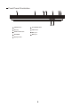
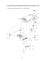
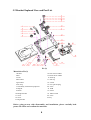
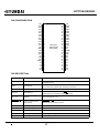
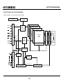
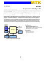
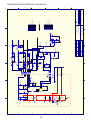
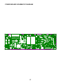
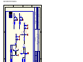
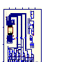
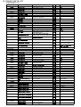
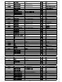
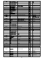
SERVICE MANUAL
DV514S
CONTENTS
1.
SAFETY PRECAUTIONS
2.
PREVENTION OF ELECTRO STATIC DISCHARGE(ESD)TO ELECTROSTATICALLY
1
SENSITIVE(ES)DEVICES
1
3.
CONTROL BUTTON LOCATIONS AND EXPLANATIONS
2
4.
PREVERTION OF STATIC ELECTRICITY DISCHARGE
3
5.
ASSEMBLING AND DISASSEMBLING THE MECHANISM UNIT
4
5.1
OPTICAL PICKUP UNIT EXPLOSED VIEW AND PART LIST
4
5.2
BRACKET EXPLOSED VIEW AND PART LIST
6
5.3
MISCELLANEOUS
7
6.
ELECTRICAL CONFIRMATION
8
6.1
VIDEO OUTPUT (LUMINANCE SIGNAL) CONFIRMATION
8
6.2
VIDEO OUTPUT(CHROMINANCE SIGNAL) CONFIRMATION
9
7.
MPEG BOARD CHECK WAVEFORM
10
8.
AM29LV160D
11
8.1
HY57V641620HG
16
8.2
MT1389
19
9.
10.
SCHEMATIC & PCB WIRING DIAGRAM
SPARE PARTS LIST
22
36
1. SAFETY PREAUTIONS
1.1 GENERAL GUIDELINES
1. When servicing, observe the original lead dress. if a short circuit is found, replace all parts which have
been overheated or damaged by the short circuit.
2. After servicing, see to it that all the protective devices such as insulation barrier, insulation papers
shields are properly installed.
3. After servicing, make the following leakage current checks to prevent the customer from being exposed
to shock hazards.
2.PREVENTION OF ELECTRO STATIC DISCHARGE(ESD)TO
ELECTROSTATICALLY SENSITIVE(ES)DEVICES
Some semiconductor(solid state)devices can be damaged easily by static electricity. Such components
commonly are called Electrostatically Sensitive(ES)Devices. Examples of typical ES devices are integrated
circuits and some field-effect transistors and semiconductor chip components. The following techniques
should be used to help reduce the incidence of component damage caused by electro static discharge(ESD).
1. Immediately before handling any semiconductor component or semiconductor-equipped assembly, drain
off any ESD on your body by touching a known earth ground. Alternatively, obtain and wear a commercially
availabel discharging ESD wrist strap, which should be removed for potential shock reasons prior to
applying power to the unit under test.
2. After removing an electrical assembly equipped with ES devices,place the assembly on a conductive
surface such as alminum foil, to prevent electrostatic charge buildup or exposure of the assembly.
3. Use only a grounded-tip soldering iron to solder or unsolder ES devices.
4. Use only an anti-static solder removal device. Some solder removal devices not classified as anti-static
(ESD protected)can generate electrical charge sufficient to damage ES devices.
5. Do not use freon-propelled chemicals. These can generate electrical charges sufficient to damage ES
devices.
6. Do not remove a replacement ES device from its protective package until immediately before you are
ready to install it. (Most replacement ES devices are packaged with leads electrically shorted together by
conductive foam, alminum foil or comparable conductive material).
7. Immediately before removing the protective material from the leads of a replacement ES device, touch
the protective material to the chassis or circuit assembly into which the device will be installed.
Caution
Be sure no power is applied to the chassis or circuit, and observe all other safety precautions.
8. Minimize bodily motions when handling unpackaged replacement ES devices. (Otherwise harmless motion
such as the brushing together of your clothes fabric or the lifting of your foot from a carpeted floor can
generate static electricity(ESD).
notice (1885x323x2 tiff)
1
Front Panel Illustration
2
3
4
8
POWER switch
6
PLAY/PAUSE button
2
Disc tray
7
STOP button
3
OPEN/CLOSE button
8
MIC 1 jack
4
IR SENSOR
9
MIC 2 jack
5
Display window
2
6
5
9
7
4.PREVENTION OF STATIC ELECTRICITY DISCHARGE
The laser diode in the traverse unit (optical pickup)may brake down due to static electricity of clothes or human
body. Use due caution to electrostatic breakdown when servicing and handling the laser diode.
4.1.Grounding for electrostatic breakdown prevention
Some devices such as the DVD player use the optical pickup(laser diode)and the optical pickup will be damaged
by static electricity in the working environment.Proceed servicing works under the working environment where
grounding works is completed.
4.1.1. Worktable grounding
1. Put a conductive material(sheet)or iron sheet on the area where the optical pickup is placed,and ground the
sheet.
4.1.2.Human body grounding
1 Use the anti-static wrist strap to discharge the static electricity from your body.
safety_3 (1577x409x2 tiff)
4.1.3.Handling of optical pickup
1. To keep the good quality of the optical pickup maintenance parts during transportation and before
installation, the both ends of the laser diode are short-circuited.After replacing the parts with new ones,
remove the short circuit according to the correct procedure. (See this Technical Guide).
2. Do not use a tester to check the laser diode for the optical pickup .Failure to do so willdamage the laser
diode due to the power supply in the tester.
4.2. Handling precautions for Traverse Unit (Optical Pickup)
1. Do not give a considerable shock to the traverse unit(optical pickup)as it has an extremely high-precise
structure.
2. When replacing the optical pickup, install the flexible cable and cut is short land with a nipper. See the
optical pickup replacement procedure in this Technical Guide. Before replacing the traverse unit, remove
the short pin for preventingstatic electricity and install a new unit.Connect the connector as short times as
possible.
3. The flexible cable may be cut off if an excessive force is applied to it.Use caution when handling the cable.
4. The half-fixed resistor for laser power adjustment cannot be adjusted. Do not turn the resistor.
3
5. Assembling and disassembling the mechanism unit
5.1 Optical pickup Unit Explosed View and Part List
Pic (1)
4
Materials to Pic (1)
No.
PARTS CODE
PARTS NAME
Q ty
14692200
SF-HD60
1
1
1EA0311A06300
ASSY, CHASSIS, COMPLETE
1
2
1EA0M10A15500
ASSY, MOTOR, SLED
1
Or
1EA0M10A15501
ASSY, MOTOR, SLED
1
3
1EA2451A24700
HOLDER, SHAFT
3
4
1EA2511A29100
GEAR, RACK
1
5
1EA2511A29200
GEAR, DRIVE
1
6
1EA2511A29300
GEAR, MIDDLE, A
1
7
1EA2511A29400
GEAR, MIDDLE, B
1
8
1EA2744A03000
SHAFT, SLIDE
1
9
1EA2744A03100
SHAFT, SLIDE, SUB
1
10
1EA2812A15300
SPRING, COMP, TYOUSEI
3
11
1EA2812A15400
SPRING, COMP, RACK
1
21
1EA0B10B20100
ASSY, PWB
1
Or
1EA0B10B20200
ASSY, PWB
1
31
SEXEA25700---
SPECIAL SCREW BIN+-M2X11
3
32
SEXEA25900---
SPECIAL SCREW M1.7X2.2
2
33
SFBPN204R0SE-
SCR S-TPG PAN 2X4
2
34
SFSFN266R0SE-
SCR S-TPG FLT 2.6X6
1
35
SWXEA15400---
SPECIAL WASHER 1.8X4 X0.25
2
Note : This parts list is not for service parts supply.
5
5.2 Bracket Explosed View and Part List
Pic (2)
Materials to Pic(2)
1.bracket
2.belt
3.screw
4.belt wheel
5.gearwheel
6.iron chip
7. Immobility mechanism equipment
8. Magnet
9. Platen
10. Bridge bracket
11. screw
12. screw
13. Big bracket
14. front silicon rubber
15. Back silicon rubber
16. Pick-up
17. Pick-up
18. switch
19. Five-pin flat plug
20. screw
21. PCB
22. motor
23. Motor wheel
24. screw
25.tray
Before going process with disassembly and installation, please carefully both
peruse the chart and confirm the materials.
6
5.3 MISCELLANEOUS
5.3.1 Protection of the LD(Laser diode)
Short the parts of LD circuit pattern by soldering.
5.3.2 Cautions on assembly and adjustment
Make sure that the workbenches,jigs,tips,tips of soldering irons and measuring instruments are
grounded,and that personnel wear wrist straps for ground.
Open the LD short lands quickly with a soldering iron after a circuit is connected.
Keep the power source of the pick-up protected from internal and external sources of electrical
noise.
Refrain from operation and storage in atmospheres containing corrosive gases (such as H2S,SO2,
NO2 and Cl2)or toxic gases or in locations containing substances(especially from the organic silicon,cyan,
formalin and phenol groups)which emit toxic gases.It is particularly important to ensure that none of the
above substances are present inside the unit.Otherwise,the motor may no longer run.
7
6.Electrical Confirmation
6.1. Video Output (Luminance Signal) Confirmation
DO this confirmation after replacing a P.C.B.
Measurement point
Mode
Disc
Video output terminal
Color bar 75%
PLAY(Title 46):DVDT-S15
PLAY(Title 12):DVDT-S01
DVDT-S15
or
DVDT-S01
Measuring equipment,tools
Confirmation value
200mV/dir,10 sec/dir
1000mVp-p±30mV
Purpose:To maintain video signal output compatibility.
1.Connect the oscilloscope to the video output terminal and terminate at 75 ohms.
2.Confirm that luminance signal(Y+S)level is 1000mVp-p±30mV
8
6.2 Video Output(Chrominance Signal) Confirmation
Do the confirmation after replacing P.C.B.
Measurement point
Mode
Disc
Video output terminal
Color bar 75%
PLAY(Title 46):DVDT-S15
PLAY(Title 12):DVDT-S01
DVDT-S15
or
DVDT-S01
Measuring equipment,tools
Screwdriver,Oscilloscope
200mV/dir,10 sec/dir
Confirmation value
621mVp-p±30mV
Purpose:To maintain video signal output compatibility.
1.Connect the oscilloscope to the video output terminal and terminate at 75 ohme.
2.Confirm that the chrominance signal(C)level is 621 mVp-p±30mV
9
7.MPEG BOARD CHECK WAVEFORM
7.1 27MHz WAVEFORM
DIAGRAM
7.2 IC VIPER22 PIN.5 WAVEFORM DIAGRAM
10
8. Am29LV160D
16 Megabit (2 M x 8-Bit/1 M x 16-Bit)
CMOS 3.0 Volt-only Boot Sector Flash Memory
DISTINCTIVE CHARACTERISTICS
■ Single power supply operation
■ Embedded Algorithms
— Full voltage range: 2.7 to 3.6 volt read and write
operations for battery-powered applications
— Regulated voltage range: 3.0 to 3.6 volt read and
write operations and for compatibility with high
performance 3.3 volt microprocessors
■ Manufactured on 0.23 µm process technology
— Fully compatible with 0.32 µm Am29LV160B device
— Embedded Erase algorithm automatically
preprograms and erases the entire chip or any
combination of designated sectors
— Embedded Program algorithm automatically
writes and verifies data at specified addresses
■ Minimum 1,000,000 write cycle guarantee
per sector
■ 20-year data retention at 125°C
■ High performance
— Reliable operation for the life of the system
— Access times as fast as 70 ns
■ Ultra low power consumption (typical values at
5 MHz)
■ Package option
— 48-ball FBGA
— 200 nA Automatic Sleep mode current
— 48-pin TSOP
— 200 nA standby mode current
— 44-pin SO
■ CFI (Common Flash Interface) compliant
— 9 mA read current
— 20 mA program/erase current
■ Flexible sector architecture
— One 16 Kbyte, two 8 Kbyte, one 32 Kbyte, and
thirty-one 64 Kbyte sectors (byte mode)
— Provides device-specific information to the
system, allowing host software to easily
reconfigure for different Flash devices
■ Compatibility with JEDEC standards
— One 8 Kword, two 4 Kword, one 16 Kword, and
thirty-one 32 Kword sectors (word mode)
— Pinout and software compatible with singlepower supply Flash
— Supports full chip erase
— Superior inadvertent write protection
■ Data# Polling and toggle bits
— Sector Protection features:
A hardware method of locking a sector to prevent
any program or erase operations within that sector
Sectors can be locked in-system or via
programming equipment
— Provides a software method of detecting program
or erase operation completion
■ Ready/Busy# pin (RY/BY#)
Temporary Sector Unprotect feature allows code
changes in previously locked sectors
■ Unlock Bypass Program Command
— Provides a hardware method of detecting
program or erase cycle completion (not available
on 44-pin SO)
■ Erase Suspend/Erase Resume
— Reduces overall programming time when issuing
multiple program command sequences
■ Top or bottom boot block configurations
available
— Suspends an erase operation to read data from,
or program data to, a sector that is not being
erased, then resumes the erase operation
■ Hardware reset pin (RESET#)
— Hardware method to reset the device to reading
array data
This Data Sheet states AMD’s current technical specifications regarding the Product described herein. This Data
Sheet may be revised by subsequent versions or modifications due to changes in technical specifications.
11
Publication# 22358
Rev: B Amendment/+3
Issue Date: November 10, 2000
PRODUCT SELECTOR GUIDE
Family Part Number
Am29LV160D
Voltage Range: VCC = 2.7–3.6 V
-70
-90
-120
Max access time, ns (tACC)
70
90
120
Max CE# access time, ns (tCE)
70
90
120
Max OE# access time, ns (tOE)
30
35
50
Speed Option
Note: See “AC Characteristics” for full specifications.
BLOCK DIAGRAM
DQ0–DQ15 (A-1)
RY/BY#
VCC
Sector Switches
VSS
Erase Voltage
Generator
RESET#
WE#
BYTE#
Input/Output
Buffers
State
Control
Command
Register
PGM Voltage
Generator
Chip Enable
Output Enable
Logic
CE#
OE#
VCC Detector
Address Latch
STB
Timer
A0–A19
Am29LV160D
12
STB
Data
Latch
Y-Decoder
Y-Gating
X-Decoder
Cell Matrix
CONNECTION DIAGRAMS
A15
A14
A13
A12
A11
A10
A9
A8
A19
NC
WE#
RESET#
NC
NC
RY/BY#
A18
A17
A7
A6
A5
A4
A3
A2
A1
A16
BYTE#
VSS
DQ15/A-1
DQ7
DQ14
DQ6
DQ13
DQ5
DQ12
DQ4
VCC
DQ11
DQ3
DQ10
DQ2
DQ9
DQ1
DQ8
DQ0
OE#
VSS
CE#
A0
1
2
3
4
5
6
7
8
9
10
11
12
13
14
15
16
17
18
19
20
21
22
23
24
1
2
3
4
5
6
7
8
9
10
11
12
13
14
15
16
17
18
19
20
21
22
23
24
Standard TSOP
Reverse TSOP
13
48
47
46
45
44
43
42
41
40
39
38
37
36
35
34
33
32
31
30
29
28
27
26
25
48
47
46
45
44
43
42
41
40
39
38
37
36
35
34
33
32
31
30
29
28
27
26
25
A16
BYTE#
VSS
DQ15/A-1
DQ7
DQ14
DQ6
DQ13
DQ5
DQ12
DQ4
VCC
DQ11
DQ3
DQ10
DQ2
DQ9
DQ1
DQ8
DQ0
OE#
VSS
CE#
A0
A15
A14
A13
A12
A11
A10
A9
A8
A19
NC
WE#
RESET#
NC
NC
RY/BY#
A18
A17
A7
A6
A5
A4
A3
A2
A1
CONNECTION DIAGRAMS
RESET#
A18
A17
A7
A6
A5
A4
A3
A2
A1
A0
CE#
VSS
OE#
DQ0
DQ8
DQ1
DQ9
DQ2
DQ10
DQ3
DQ11
1
2
3
4
5
6
7
8
9
10
11
12
13
14
15
16
17
18
19
20
21
22
44
43
42
41
40
39
38
37
36
35
34
33
32
31
30
29
28
27
26
25
24
23
SO
WE#
A19
A8
A9
A10
A11
A12
A13
A14
A15
A16
BYTE#
VSS
DQ15/A-1
DQ7
DQ14
DQ6
DQ13
DQ5
DQ12
DQ4
VCC
FBGA
Top View, Balls Facing Down
A6
B6
C6
D6
E6
A13
A12
A14
A15
A16
A5
B5
C5
D5
E5
F5
G5
H5
A9
A8
A10
A11
DQ7
DQ14
DQ13
DQ6
A4
B4
C4
D4
E4
F4
G4
H4
WE#
RESET#
NC
A19
DQ5
DQ12
VCC
DQ4
A3
B3
C3
D3
E3
F3
G3
H3
RY/BY#
NC
A18
NC
DQ2
DQ10
DQ11
DQ3
A2
B2
C2
D2
E2
F2
G2
H2
A7
A17
A6
A5
DQ0
DQ8
DQ9
DQ1
A1
B1
C1
D1
E1
F1
G1
H1
A3
A4
A2
A1
A0
CE#
OE#
VSS
Special Handling Instructions
Special handling is required for Flash Memory products
in FBGA packages.
A
14
F6
G6
BYTE# DQ15/A-1
H6
VSS
Flash memory devices in FBGA packages may be
damaged if exposed to ultrasonic cleaning methods.
The package and/or data integrity may be compromised
if the package body is exposed to temperatures above
150°C for prolonged periods of time.
PIN CONFIGURATION
A0–A19
LOGIC SYMBOL
= 20 addresses
20
DQ0–DQ14 = 15 data inputs/outputs
DQ15/A-1
A0–A19
= DQ15 (data input/output, word mode),
A-1 (LSB address input, byte mode)
16 or 8
DQ0–DQ15
(A-1)
BYTE#
= Selects 8-bit or 16-bit mode
CE#
= Chip enable
CE#
OE#
= Output enable
OE#
WE#
= Write enable
RESET#
= Hardware reset pin
RY/BY#
= Ready/Busy output
(N/A SO 044)
WE#
RESET#
BYTE#
VCC
= 3.0 volt-only single power supply
(see Product Selector Guide for speed
options and voltage supply tolerances)
VSS
= Device ground
NC
= Pin not connected internally
15
RY/BY#
(N/A SO 044)
HY57V641620HG
4 Banks x 1M x 16Bit Synchronous DRAM
8.1 HY57V641620HG
DESCRIPTION
The Hyundai HY57V641620HG is a 67,108,864-bit CMOS Synchronous DRAM, ideally suited for the main memory applications which
require large memory density and high bandwidth. HY57V641620HG is organized as 4banks of 1,048,576x16.
HY57V641620HG is offering fully synchronous operation referenced to a positive edge of the clock. All inputs and outputs are synchronized with the rising edge of the clock input. The data paths are internally pipelined to achieve very high bandwidth. All input and output
voltage levels are compatible with LVTTL.
Programmable options include the length of pipeline (Read latency of 2 or 3), the number of consecutive read or write cycles initiated
by a single control command (Burst length of 1,2,4,8 or Full page), and the burst count sequence(sequential or interleave). A burst of
read or write cycles in progress can be terminated by a burst terminate command or can be interrupted and replaced by a new burst
read or write command on any cycle. (This pipelined design is not restricted by a `2N` rule.)
FEATURES
•
Single 3.3±0.3V power supply Note)
•
Auto refresh and self refresh
•
All device pins are compatible with LVTTL interface
•
4096 refresh cycles / 64ms
•
JEDEC standard 400mil 54pin TSOP-II with 0.8mm
of pin pitch
•
Programmable Burst Length and Burst Type
•
All inputs and outputs referenced to positive edge of
system clock
- 1, 2, 4, 8 or Full page for Sequential Burst
•
Data mask function by UDQM or LDQM
•
Internal four banks operation
- 1, 2, 4 or 8 for Interleave Burst
•
.
16
Programmable CAS Latency ; 2, 3 Clocks
HY57V641620HG
PIN CONFIGURATION
VDD
DQ0
VDDQ
DQ1
DQ2
VSSQ
DQ3
DQ4
VDDQ
DQ5
DQ6
VSSQ
DQ7
VDD
LDQM
/WE
/CAS
/RAS
/CS
BA0
BA1
A10/AP
A0
A1
A2
A3
VDD
1
2
3
4
5
6
7
8
9
10
11
12
13
14
15
16
17
18
19
20
21
22
23
24
25
26
27
54
53
52
51
50
49
48
47
46
45
44
43
42
41
40
39
38
37
36
35
34
33
32
31
30
29
28
54pin TSOP II
400mil x 875mil
0.8mm pin pitch
VSS
DQ15
VSSQ
DQ14
DQ13
VDDQ
DQ12
DQ11
VSSQ
DQ10
DQ9
VDDQ
DQ8
VSS
NC
UDQM
CLK
CKE
NC
A11
A9
A8
A7
A6
A5
A4
VSS
PIN DESCRIPTION
PIN
PIN NAME
DESCRIPTION
CLK
Clock
The system clock input. All other inputs are registered to the SDRAM on the
rising edge of CLK
CKE
Clock Enable
Controls internal clock signal and when deactivated, the SDRAM will be one
of the states among power down, suspend or self refresh
CS
Chip Select
Enables or disables all inputs except CLK, CKE and DQM
BA0,BA1
Bank Address
Selects bank to be activated during RAS activity
Selects bank to be read/written during CAS activity
A0 ~ A11
Address
Row Address : RA0 ~ RA11, Column Address : CA0 ~ CA7
Auto-precharge flag : A10
RAS, CAS, WE
Row Address Strobe,
Column Address Strobe,
Write Enable
RAS, CAS and WE define the operation
Refer function truth table for details
LDQM, UDQM
Data Input/Output Mask
Controls output buffers in read mode and masks input data in write mode
DQ0 ~ DQ15
Data Input/Output
Multiplexed data input / output pin
VDD/VSS
Power Supply/Ground
Power supply for internal circuits and input buffers
VDDQ/VSSQ
Data Output Power/Ground
Power supply for output buffers
NC
No Connection
No connection
17
HY57V641620HG
FUNCTIONAL BLOCK DIAGRAM
1Mbit x 4banks x 16 I/O Synchronous DRAM
Self refresh logic
& timer
Internal Row
counter
1Mx16 Bank 3
CLK
Row active
Column
Pre
Decoders
UDQM
Y decoders
LDQM
Bank Select
A0
A1
Column Add
Counter
Address
Registers
Address buffers
A11
BA0
BA1
Memory
Cell
Array
Burst
Counter
Mode Registers
CAS Latency
18
Data Out Control
Pipe Line Control
DQ0
I/O Buffer & Logic
Column
Active
1Mx16 Bank 0
Sense AMP & I/O Gate
WE
refresh
1Mx16 Bank 1
X decoders
CAS
1Mx16 Bank 2
X decoders
RAS
State Machine
CS
Row
Pre
Decoders
X decoders
X decoders
CKE
DQ1
DQ14
DQ15
MT1389
8.2 MT1389
Progressive-Scan DVD Player SOC
Specifications are subject to change without notice
MediaTek MT1389 is a DVD player system-on-chip (SOC) which incorporates advanced features like high
quality TV encoder and state-of-art de-interlace processing. The MT1389 enables consumer electronics
manufacturers to build high quality, cost-effective DVD players, portable DVD players or any other home
entertainment audio/video devices.
Based on MediaTek’s world-leading DVD player SOC architecture, the MT1389 is the 3rd generation of the DVD
player SOC. It integrates the MediaTek 2nd generation front-end analog RF amplifier and the Servo/MPEG AV
decoder.
The progressive scan of the MT1389 utilized a proprietary advanced motion-adaptive de-interlace algorithm to
achieve the best movie/video playback. It can easily detect 3:2/2:2 pull down source and restore the correct
original pictures. It also supports a patent-pending edge-preserving algorithm to remove the saw-tooth effect.
Key Features
DVD
PUH
Module
CVBS, Y/C,
Component
MT1389L
Applications
FLASH
Front-panel
Remote
SDPIF
RF/Servo/MPEG Integration
High Performance Audio Processor
Motion-Adaptive, Edge-Preserving De-interlace
108MHz/12-bit, 6 CH TV Encoder
Audio DAC
DRAM
DVD Player System Diagram Using MT1389
19
Standard DVD Players
Portable DVD Players
MT1389
PRELIMINARY, SUBJECT TO CHANGE WITHOUT NOTICE
MTK CONFIDENTIAL, NO DISCLOSURE
General Feature List
Super Integration DVD player single chip
High performance analog RF amplifier
Servo controller and data channel processing
MPEG-1/MPEG-2/JPEG video
Dolby AC-3/DTS/DVD-Audio
Unified memory architecture
Versatile video scaling & quality
enhancement
OSD & Sub-picture
2-D graphic engine
Built-in clock generator
Built-in high quality TV encoder
Built-in progressive video processor
Audio effect post-processor
Audio input port
High Performance Analog RF Amplifier
Programmable fc
Dual automatic laser power control
Defect and blank detection
RF level signal generator
Speed Performance on Servo/Channel Decoding
DVD-ROM up to 4XS
CD-ROM up to 24XS
Channel Data Processor
Digital data slicer for small jitter capability
Built-in high performance data PLL for
channel data demodulation
EFM/EFM+ data demodulation
Enhanced channel data frame sync protection
& DVD-ROM sector sync protection
Servo Control and Spindle Motor Control
Programmable frequency error gain and
phase error gain of spindle PLL to control
spindle motor on CLV and CAV mode
Built-in ADCs and DACs for digital servo
control
Provide 2 general PWM
Tray control can be PWM output or digital
output
Embedded Micro controller
Built-in 8032 micro controller
Built-in internal 373 and 8-bit programmable
lower address port
20
1024-bytes on-chip RAM
Up to 4M bytes FLASH-programming
interface
Supports 5/3.3-Volt. FLASH interface
Supports power-down mode
Supports additional serial port
DVD-ROM/CD-ROM Decoding Logic
High-speed ECC logic capable of correcting
one error per each P-codeword or
Q-codeword
Automatic sector Mode and Form detection
Automatic sector Header verification
Decoder Error Notification Interrupt that
signals various decoder errors
Provide error correction acceleration
Buffer Memory Controller
Supports 16Mb/32Mb/64Mb/128Mb SDRAM
Supports 16-bit SDRAM data bus
Provide the self-refresh mode SDRAM
Block-based sector addressing
Support 3.3 Volt. DRAM Interface
Video Decode
Decodes MPEG1 video and MPEG2 main level,
main profile video (720/480 and 720x576)
Smooth digest view function with I, P and B
picture decoding
Baseline, extended-sequential and
progressive JPEG image decoding
Support CD-G titles
Video/OSD/SPU/HLI Processor
Arbitrary ratio vertical/horizontal scaling of
video, from 0.25X to 256X
65535/256/16/4/2-color bitmap format OSD,
256/16 color RLC format OSD
Automatic scrolling of OSD image
Slide show transition as DVD-Audio
Specification
2-D Graphic Engine
Support decode Text and Bitmap
Support line, rectangle and gradient fill
Support bitblt
Chroma key copy operation
Clip mask
MT1389
PRELIMINARY, SUBJECT TO CHANGE WITHOUT NOTICE
MTK CONFIDENTIAL, NO DISCLOSURE
Audio Effect Processing
Dolby Digital (AC-3)/EX decoding
DTS/DTS-ES decoding
MLP decoding for DVD-Audio
MPEG-1 layer 1/layer 2 audio decoding
MPEG-2 layer1/layer2 2-channel audio
High Definition Compatible Digital (HDCD)
Windows Media Audio (WMA)
Advanced Audio Coding (AAC)
Dolby ProLogic II
Concurrent multi-channel and downmix out
IEC 60958/61937 output
- PCM / bit stream / mute mode
- Custom IEC latency up to 2 frames
Pink noise and white noise generator
Karaoke functions
- Microphone echo
- Microphone tone control
- Vocal mute/vocal assistant
- Key shift up to +/- 8 keys
- Chorus/Flanger/Harmony/Reverb
Channel equalizer
3D surround processing include virtual
surround and speaker separation
21
TV Encoder
Six 108MHz/12bit DACs
Support NTSC, PAL-BDGHINM, PAL-60
Support 525p, 625p progressive TV format
Automatically turn off unconnected channels
Support PC monitor (VGA)
Support Macrovision 7.1 L1, Macrovision
525P and 625P
CGMS-A/WSS
Closed Caption
Progressive Output
Automatic detect film or video source
3:2 pull down source detection
Advanced Motion adaptive de-interlace
Edge Preserving
Minimum external memory requirement
Audio Input
Line-in/SPDIF-in for versatile audio
processing
Outline
256-pin LQFP package
3.3/1.8-Volt. Dual operating voltages
A
B
C
D
E
F
From MPEG Board
1
1
2
3
4
5
XS401
1
2
3
4
5
6
7
7PIN/2.0
XS402
5PIN/2.0
2PIN/2.0
C409
101
IR
BEAD1 STB
CLOCK
DATE
LED_B
L402
BEAD1
L401
D402
C410 IN4148
C411
102
101
VCC
2
1K
R410
R412
10K
VCC
POWER_LED
Seg2
KEY1
D401
LED
VCC
V401
8050D
R409
33R(1/4W)
O/C
K401
Stop
K402
LED403
LED
C405
104
3
Seg4
Seg5
Seg6
Seg1
Seg2
Seg3
DATE
CLOCK
STB
KEY1
KEY2
KEY3
51K
1
2
3
4
5
6
7
8
9
10
11
12
13
14
15
16
R405
3
U401
PT6961
LED402
LED_MODULE_ZDC6-2004YRGB-A
4
日期
6.24
4
OSC
GND
DOUT
GR1
DIN
GR2
CLK
GND
STB
GR3
K1
GR4
K2
GND
K3
VDD
VDD
GR5
SEG1/KS1
GR6
SEG2/KS2 SEG12/GR7
SEG3/KS3
SEG11
NC
SEG10/KS10
SEG4/KS4
SEG9/KS9
SEG5/KS5
SEG8/KS8
SEG6/KS6
SEG7/KS7
更改 数量 更改单号 签 名
设 计
Zhiyong Deng
审 核
标准化
批 准
R414
220
LED404
LED
VCC
R413
220
R408
0R/NC
IN4148
LED401
LED(backgroud)
470
R411
Seg1
Play
1
2
VCC
DATE
CLOCK
K403
C403
101
C402
101
C401
101
STB
XS403
10K
R403
10K
R402
10K
R401
2
Grid1
32
31
30
29
28
27
26
25
24
23
22
21
20
19
18
17
5
板号: 4975-0
5
主面板电原理图
C408
104
VCC
U402
HS0038B3V
IR
质量
共 1 张
C407
101
6
数量
版次:1.0
6
广东步步高电子工业有限公司AV厂
比例
第 1 张
BBK
10K
DZ401
3.3V/0.5W/option
R406
C406
104
100
TC401
100uF/16V
R407
DV975
VCC
Seg9
Seg8
Seg7
Grid5
Grid6
Grid7
LED
Grid3
Grid4
Grid1
Grid2
1
Grid1
Grid2
2
Grid2
TC402
VCC
1
2
Grid3
3
Grid3
Grid4
4
Grid4
Grid5
5
Grid5
Grid6
6
Grid6
Grid7
7
Grid7
Seg1/ks1
8
Seg1
Seg2/ks2
9
Seg2
Seg3/ks3
10
Seg3
Seg4/ks4
11
Seg4
Seg5/ks5
12
Seg5
Seg6/ks6
13
Seg6
Seg7/ks7
14
Seg7
Seg8/ks8
15
Seg8
Seg9/ks9
16
100uF/16V
Seg9
3
22
1
2
1
A
B
C
D
E
F
9.0 SCHEMATIC & PCB WIRING DIAGRAM
FRONT SCHEMATIC DIAGRAM
FRONT SCHEMATIC DIAGRAM
23
24
A
B
C
D
1
1
24
XS901
5PIN/2.0
1
2
3
4
5
XS902
2PIN/2.0
1
2
LED901
LED(backgroud)
2
日期
K901
STANDBY
更改 数量 更改单号 签 名
设 计
Zhiyong Deng
审 核
标准化
批 准
2
DV975A
3
板号 : 4975A-0
主面板电原理图
3
质量
共 1 张
数量
版次:1.0
4
广东步步高电子工业有限公司AV厂
比例
第 1 张
BBK
4
A
B
C
D
SUBSIDIART BOARD SCHEMATIC DIAGRAM
SUBSIDIART BOARD SCHEMATIC DIAGRAM
25
F
E
D
C
B
1
F502
!
BCN502
SW-SPST
T1.6AL250V
!
!
!
!
D501
1N4007
!
1
!
F501
T1.6AL250V
1
2
L501
4
BCN501
~220V
BCN503
~220V
2
1
3
2
U501
VIPER22
R501
680K 1/2W
L503
FB
TC501
47uF/400V
BC501
~275V 104
D504
1N4007
D503
1N4007
2
5
6
7
8
2
VDD
FB
D
D
D
D
S
S
D502
1N4007
2
1
2
1
26
1
2
A
1
4
3
C503
101/1KV
R503
39K/2W
C506
473
C504
104
R512
9.1K
TC502
47uF/50V
R505
33R
D505
HER107
C502
103/1KV
!
3
4
U502
PH817
2
1
BC505
~275V 221
2
BC504
~275V 221
1
T501
10
7
3
BCK-28-519S
11
6
BC503
~275V 221
!
D506
HER105
12
4
15
13
9
16
3
2
!
3
14
2
1
R506
330
1K(NC)
R517
R507
1K(NC)
D511
HER105
D512
HER105
C519 104
HER303
C516
104
R5161K(NC)
D513
SR303
C518
104
D510
JP504
0R(NC)
D507
HER105
D508
HER105
U503
LM431A
TC512
47uF/50V
TC511
100uF/16V
A
K
JP501
0R
R502
0R
C515
104
R509
10K/1%
R508
3.3K/1%
JP502
0R
更改 数量 更改单号
设 计
审 核
标准化
批 准
4
C517
104
JP506
0R(NC)
FL-
FL+
C511
104
TC508
470uF/10V(nc)
L509
10uH/1A(option)
C508
104
C510
104
TC506
1000uF/10V
0R(NC)
JP505
TC504
470uF/16V
TC510
1000uF/10V
2.5V
R
0R(NC)
JP519
JP508
0R(NC)
TC514
1000uF/10V
L508
10uH/2A
TC505
1000uF/10V
L507
10uH/2A
TC515
1000uF/10V
LED+5V
TC503
470uF/16V
L505
10uH/1A
4
签 名
ZD502
10V/0.5W
R511
1.5K
+3.3V
+5V
SA+5V
日期
2004.4.16
Q501
8550D
R515
220R/1/4W
ZD501
5.1V/0.5W
R514
220
R513
1K
+9V
5
TC507
47uF/16V
JP507
0R(NC)
-21V
5
数量
版次: 1.0
6
广东步步高电子工业有限公司AV厂
质量
共 1 张
板号: 5977SB
BBK
To Microphone Board
CN501
13P2.0mm
CN503
2P2.0mm
CN502
11P2.0mm
To Mpeg Board
比例
第 1 张
DV977
1
2
3
4
5
6
7
8
9
10
11
12
13
1
2
1
2
3
4
5
6
7
8
9
10
11
开关电源电原理图
C512
104
-9V
AGND
MIC-DET
OKA
AGND
+9V
-9V
GND
+5V
GND
+3.3V
FL+
FL-21V
LED+5V
GND
MIC-DET
OKA
AGND
+9V
-9V
GND
+5V
GND
+3.3V
GND
SA+5V
6
F
E
D
C
B
A
POWER BOARD SCHEMATIC DIAGRAM
POWER BOARD SCHEMATIC DIAGRAM
27
28
A
B
C
CK3-6.35-24
MIC601
MIC602 4
3
2
1
CK3-6.35-24
1
BEAD
L604
L601
BEAD
BEAD
L603
L602
BEAD
C603
103
R604
560R
C604
103
TC602
4.7uF/16V
R602
22K
R608
1K
R607
1K
R603
560R
TC606
22uF/16V
R601
22K
TC601
4.7uF/16V
TC605
22uF/16V
R606
10K
5
6
R605
10k
3
2
C605
100p
4
8
1
-9VA
GND602
GND
TC604
4.7uF/16V
GND601
GND
7
TC603
4.7uF/16V
R618
10K
R623
10K
R611
5.1K
R612
5.1K
2
更改 数量 更改单号 签 名
设 计
Z.Y.Deng
审 核
标准化
批 准
U601B
4558
C606
100p
R610
10K
+9VA
4558
U601A
R609
10K
2
R616
330
R615
100K
日期
+5V
3
2
C607
R613
5.1K
4
8
D
1
5
6
100P
1
+9VA
U602B
4558
7
DV975
100
R619
C608
102
4.7uF/16V
TC613
3
板号 : 6975A-0
C601
104
+9VA
C602
104
-9VA
6P2.0mm
1
2
3
4
5
6
XS601
+5V
-9V
+9V
AGND
OK
DET
比例
第 1 张
质量
共 1 张
数量
版次: 1.0
BBK AV RD3
R620
1K
DET
TC615
47uF/16V
R621
10ohm 1/6W
TC616
47uF/16V
R622
10ohm 1/6W
4
4
广东步步高电子工业有限公司AV厂
+9V
-9V
VD602TC611
IN414847uF/16V
IN4148
VD603
VD601
IN4148
+5V
R617
100K
OK
MIC板电原理图
U602A
4558
-9VA
3
A
B
C
D
OK SCHEMATIC DIAGRAM
OK SCHEMATIC DIAGRAM
29
F
E
D
C
B
1
XS03
XS702
3
2
1
L
AGND
R
PDAT0
PDAT2
R704
4.7K
VCC
VGND
XS28
XS701
1
2
3
4
5
6
7
8
9
10
11
12
13
14
15
16
17
18
19
20
21
22
23
24
25
26
27
28
IN4148
IN4148
D701
D702
2
R714
2.2K
VGND
R713 0R
R715 0R
VGND
AGND
AGND
LFE
+10V
CC
SR
SL
R
VIEDO
PDAT0
L
Pb
Y1
Pr
C
C707
105
R705
75R
PDAT2
PDAT1
SPDIF
VCC
Y
AGND
V703
8050
R711
1K
A+10V
AGND
C723
102
V702
8050
R708
33R
A+10V
AGND VGND
C724
102
R712
2.2K
2.2K
R710
330R
+10V
R709
C727
102
V701
8050
C
Y
C719
TC706
TC705
C718
VIEDO
AGND
VGND
L711
FBSMT
104
104
FBSMT
220uF/16V
L712
220uF/16V
104
C721
2.2R
R706
3
VGND
5.1V/0.5W
ZD703
5.1V/0.5W
ZD702
5.1V/0.5W
ZD701
ZD704
5.1V/0.5W
AGND
L714 FCM
C726
AGND
104
L713 FCM
TC701
220uF
R715
47K
C716 102
VCC
3
VJS3921
2
VGND
105
105
1
2
6
5
VGND
C713
20
18
16
14
12
10
8
6
4
C712
L715 FBSMT
L716 FBSMT
VGND
68R
R703
A(B)OUT
A(B)IN
A(A)OUT
A-COM
RETURN
A(A)IN
BLUE I/O
FUNC SW
RETURN
CONT
GREEN I/O
NC
RETURN
RETURN
RED I/O
BLK I/O
RETURN
TRTURN
V-OUT
V-IN
GND
JK706
FBSMT
L710
SPDIF
21
19
17
15
13
11
9
7
5
3
1
104
C725
C711
104
AGND
S-VIDEO
JK703A
JK703B
S-OUT
VCC
VGND
C728
104
A+10V
7
2
3
30
4
A
1
3
2
更改 数量 更改单号
设 计
审 核
标准化
批 准
4
GND
VCC
JK705
OPTICAL
1
VIN
4
签 名
Pr
Pb
SPDIF
Y1
日期
FBSMT
5
VGND
LFDV965
FBSMT
L708
FBSMT
L707
AGND
板号: 7969BSB
AV 输出板原理图
220uF/16V R
C722 104
TC704
C706
102
C705
102
C704
102
C703
102
C702
102
C701
102
L709
R702 100R
220R
R701
G
FB
L706
FB
L705
FB
L704
FB
L703
FB
L702
FB
L701
220uF/16V B
VGND
C717 104
TC703
C710
104
TC702
1000uF/10V
C720 104
R
L
SR
SL
LFE
CC
5
12
10
3
11
8
5
2
5
2
RED
WHITE
JK701
AV8
质量
共 1 张
数量
版次:1.0
6
广东步步高电子工业有限公司AV厂
RED
BLUE
BLACK
GREEN
比例 1:1
第 1 张
BBK
RCA-407
6
4
3
1
JK702
9
7
6
4
1
6
F
E
D
C
B
A
OUTPUT BOARD SCHEMATIC DIAGRAM
OUTPUT BOARD SCHEMATIC DIAGRAM
31
F
E
D
C
B
A
R319
150K
C305
104
C303
104
1
AGND
22
23
24
25
26
27
28
V307
8050D
V306
8550D
VGND
2.2R\1/4W
R326
R325
(TRCLOSE1)
510R
TROPEN
LOAD-
R323
1.5K
R340 1R(DNS)
TC308
47uF/16V
222
680K
R320
150K C308
101(DNS)
R317
C307
TRSO
V1P4
STBY
20K
151
R313
10K
R321
1R
C304
GND
FMSO
R312
SL+
SLVCC
C302
104
C312
104
C311
104
VCC
V310
9014-S
R327
510R
R324
1.5K
V1P4
SP-
C310
222
ADIN
OPOP+
OPO
VINFFC
VOSL
VINSLVINSL+
CF2
CF1
VINFC
V309
8550D
V308
8050D
R322
680K
R318 0R
U302
BA5954
PREGND
VINLD
CTK2
CTK1
VINTK
BIAS
STBY
VOFC+
VOFCVO2+
VOSLPGND
PVCC1
VCC
F
B
A
RFO
IOA
D
C
V20
E
MDI1
C301
104
100K
AVCC
R310
VOTK+
VOTKVOLD+
VOLDPGND
VNFTK
PVCC2
R303
L312
L314
L316
L317
L318
L319
L320
L321
L322
L323
L324
15
16
17
18
19
20
21
0R
FBSMT
FBSMT
FBSMT
FBSMT
FBSMT
FBSMT
FBSMT
FBSMT
FBSMT
FBSMT
FBSMT
L310
L311
R304
1R
FBSMT
FBSMT
L304
L305
L306
L307
L308
FBSMT
4.7uH
FBSMT
FBSMT
4.7uH
FBSMT
FBSMT
L301
L303
V304
2SK3018-S
24
23
22
21
20
19
18
17
16
15
14
13
12
11
10
9
8
7
6
5
4
3
2
1
V303
XS301 2SK3018-S
24P0.5mm
R305
1R
V305
3904-S
IOA
10K
R339
(TRCLOSE1)
TROPEN
(TROPEN1)
TRCLOSE
LOAD+
V18
C306
151
L235
FBSMT
89V33
2
DV33
R330
10K
R329
10K
102
C253
104
TRO
FOO
105
C333
102
C255
C250
104
TDI
TMS
TCK
TDO
3
105
C330
GND
C249
104
C215
152
USBVDD
ADIN
TROUT
TRIN
STBY
TRCLOSE
V18
A2
A3
A4
A5
A6
A7
A8
A18
A19
18K
20K
L202
33R
105
C331
MDI1
MDI2
FEO
TEO
TEZISLV
OPO
OPOP+
10K DMO
15K FMO
TROPEN
RFOP
RFON
0R(DNS)
0R
0R
0R
0R
0R
R221 330R TROUT
R277 330R TRIN
C252
104
89V33
C240
105
105(DNS)
105
105
105
105
C229
104
C238
104
R228
C248
104
C258
104
C214
104
C213
331
C247
104
R212
0R
C257
104
C246
104
C294
C251
104
C245
104
C309
104
C244
104
AVDD3
L236 FBSMT
DV33
C256
104
L201
FBSMT
C212
331
R210
R211
DMSO R208
FMSO R209
C207
104
R2165
V2P8
V20
V1P4
LDO2
LDO1
DV33
E
F
R201
R202
R203
R204
C205
C204
D
C206
101
C203
C202
B
A
C201
C
C
B
A
D
SUBA
SUBB
SUBC
SUBD
RFO
R2166
0R(DNS)
C211
89V33 104
C210
153
V1P4
C2174
104
XS302
5P2.0mm
1
LOAD2
LOAD+
3
4 GND
5
C297
102
LIMIT
C254
104
105
C322
TRSO
FOSO
105
C321
105
C318
C317
105
105
105
C320
C319
C230
104
L234
RFV18
FBSMT
104
C237
104
C243
104
R281 330R
C2167
104
R316 20K
R315
20K
SPSP+
DMSO
R306
1R
104
C236
C241
C242
104
R307
1R
TC303
47uF/16V
LDO-AV33
R2164
10K
GND
SP+
SL+
SL-
FOSO
V1P4
TC309
47uF/16V
1
2
3
4
5
6
XS303
XS06
7
6
5
4
3
2
1
14
13
12
11
10
9
8
DQS0
V302
2SB1132-S LDO1
V301
2SB1132-S
R331 0R
104
C235
L309
DV33V18
FBSMT
104
C234
TC302
47uF/16V
LDO2
LDO-AV33
VCC
R302
10R
R301
10R
TC301
220uF/16V
104
C231
DV33
VREFN
PWR#
PCE#
PRD#
105
C332
1
2
3
4
5
6
7
8
9
10
11
12
13
14
15
16
17
18
19
20
21
22
23
24
25
26
27
28
29
30
31
32
33
34
35
36
37
38
39
40
41
42
43
44
45
46
47
48
49
50
51
52
53
54
55
56
57
58
59
60
61
62
63
64
C239
104
AVDD3
AGND
DVDA
DVDB
DVDC
DVDD
DVDRFIP
DVDRFIN
MA
MB
MC
MD
SA
SB
SC
SD
CDFON
CDFOP
TNI
TPI
MDI1
MDI2
LDO2
LDO1
SVDD3
CSO/RFOP
RFLVL/RFON
SGND
V2REFO
V20
VREFO
FEO
TEO
TEZISLV
OP_OUT
OP_INN
OP_INP
DMO
FMO
TROPENPWM
PWMOUT1/V_ADIN9
TRO
FOO
USB_VSS
USBP
USBM
USB_VDD3
FG/V_ADIN8
TDI/V_ADIN4
TMS/V_ADIN5
TCK/V_ADIN6
TDO/V_ADIN7
DVDD18
IOA2
IOA3
IOA4
IOA5
IOA6
IOA7
HIGHA0
IOA18
IOA19
DVSS
APLLCAP
APLLVSS
R297
R298
R299
104
C2175 C2175
104
R224
C228
104
C227
104
C226
104
C225
333
C224
104
0R
0R
0R
DWR#
DCE#
DRD#
PWR#
A16
A15
A14
A13
A12
A11
10K
100K
4
V1P4 C222
C223 20pF
102
DV33
VREFN
VREFP
A10
A9
A20
PCE#
A1
PRD#
R223
15K
VREFP
TC202
10uF/16V
C220
473
C219
473
C221 105
DV33
AD0
AD1
AD2
AD3
3
DV33
AD4
AD5
AD6
A21
2
JITFN C218 474
JITFO
XI
XO
RFV18
MT1389
U201
AD7
A17
A0
AVCC
ASPDIF
AMDAT
V18
10K
R311
RESET#
V18
MUTE_DAC
ASDAT2
ASDAT1
ASDAT0
VSCK
VSDA
VSTB
SCL
SDA
R309
5
ACLK
ABCK
ALRCK
89V33
RXD
TXD
100K
R215
1K
FS0
FS1
URST#
IR
R308
DQM0
DQS0
DQ7
1
Y6
Y5
DQ6
DQ5
29
30
Y4
DQ4
DQ3
GND
GND
R227
JITFO C233
Y2
Y3
6
JITFN
R213
1K
192
191
190
189
188
187
186
185
184
183
182
181
180
179
178
177
176
175
174
173
172
171
170
169
168
167
166
165
164
163
162
161
160
159
158
157
156
155
154
153
152
151
150
149
148
147
146
145
144
143
142
141
140
139
138
137
136
135
134
133
132
131
130
129
Y0
510R
DMA8
DMA9
DMA11
DCKE
DCLK
DMA7
DMA4
DMA5
DMA6
DQ27
DQ28
DQ29
DQ30
DQ31
DQ26
DQ22
DQ23
DQM2
DQM3
DQ24
DQ25
DQ17
DQ18
DQ19
DQ20
DQ21
DQ9
DQ10
DQ11
DQ12
DQ13
RAS#
CAS#
WE#
DQM1
LIMIT
DQ8
BA0
CS#
DMA0
DMA10
BA1
DMA3
DMA2
DMA1
DCLKB
DQ16
R214
FS
C216
105
C329
104
105
104
89V33 V18
C328
C217
L203
DACVDD3 FBSMTDV33
VOICE-DET
R2160 0R(DNS)
HSYNC#
VSYNC#
750K
101
YUV0/CIN
FS
VREF
DACVDDC
RD16
RD17
RD18
RD19
RD20
RD21
DVDD3
RD22
RD23
DQM2
DQM3
RD24
RD25
DVSS
RD26
DVDD18
RD27
RD28
RD29
RD30
RD31/ASDATA5
DVDD3
RA4
RA5
RA6
DVSS
RA7
DVSS
RA8
RA9
RA11
CKE
RCLK
DVDD3
RCLKB
RVREF/V_ADIN3
DVDD18
RA3
RA2
RA1
DVSS
RA0
RA10
BA1
DVSS
BA0
RCS
DVDD3
RAS
CAS
RWE
DQM1
DQS1
RD8
DVSS
RD9
RD10
RD11
DR12
RD13
DQ2
DQ1
DQ0
DQ15
R314 10K
Y1
256
255
254
253
252
251
250
249
248
247
246
245
244
243
242
241
240
239
238
237
236
235
234
233
232
231
230
229
228
227
226
225
224
223
222
221
220
219
218
217
216
215
214
213
212
211
210
209
208
207
206
205
204
203
202
201
200
199
198
197
196
195
194
193
AVDD3
IREF
RFGC
OSN
OSP
CEQN
CEQP
RFGND
CRTPLP
HRFZC
RFRPAC
RFRPDC
RFVDD3
S_VREFN
S_VREFP
ADCVSS
S_VCM
ADCVDD3
LPFOP
LPFIN
LPFIP
LPFON
PLLVDD3
IDACEXLP
PLLVSS
JITFN
JITFO
XTALI
XTALO
RFVDD18
RFGND18
SPDIF
MC_DATA
DVSS
ASDATA4
DVDD18
ASDATA3
ASDATA2
ASDATA1
ASDATA0
DVSS
ACLK
ABCK
ALRCK
DVDD3
SPBCK/ASDATA5
SPLRCK
SPDATA
SPMCLK
HSYNC/V_ADIN2
YUV7/ASDATA5
VSYNC/V_ADIN1
DVDD3
YUV6/R
YUV5/B
DACVSSA
YUV4/G
DACVDDA
YUV3/CVBS
DACVSSB
YUV2/C
DACVDDB
YUV1/Y
DACVSSC
APLLVDD3
IOWR
A16
HIGHA7
HIGHA6
HIGHA5
HIGHA4
HIGHA3
DVDD3
HIGHA2
HIGHA1
IOA20
IOCS
IOA1
IOOE
DVDD3
AD0
AD1
AD2
AD3
DVSS
AD4
AD5
AD6
IOA21/V_ADIN0
ALE
AD7
A17
IOA0
DVSS
UWR
URD
DVDD18
UP1_2
UP1_3
UP1_4
UP1_5
UP1_6
UP1_7
UP3_0
UP3_1
UP3_4
UP3_5
DVDD3
ICE
PRST
IR
INT0
DQM0
DQS0
RD7
DVSS
RD6
RD5
DVSS
RD4
RD3
DVDD18
RD2
RD1
RD0
RD15
DVDD3
RD14
65
66
67
68
69
70
71
72
73
74
75
76
77
78
79
80
81
82
83
84
85
86
87
88
89
90
91
92
93
94
95
96
97
98
99
100
101
102
103
104
105
106
107
108
109
110
111
112
113
114
115
116
117
118
119
120
121
122
123
124
125
126
127
128
DQ14
32
F
E
D
C
B
A
B
F
E
D
C
XS201
7
6
5
4
3
2
1
A
AGND
FS1
1
2
3
4
DV33
75R
R233
1
2
3
4
5
6
7
8
9
10
11
12
13
1
AGND
+9V
DV33
RXD
TXD
GND
L225
1K(DNS)
C324
R237
0R
0R(DNS)
R236
102
VIDEO_COMP
R234
75R
VIDEO_U
VIDEO_Y1
VIDEO_V
VIDEO_C
VCC
VIDEO_Y
HSYNC#
VSYNC#
ASTB
VGND AGND
LFE
Cc
SR
SL
Rt
Lt
NC
NC
DQMH
DQML
WE
CAS
RAS
CS
CKE
CLK
A0
A1
A2
A3
A4
A5
A6
A7
A8
A9
A10
BA/A11
1
2
3
4
5
6
7
8
9
10
11
12
13
14
15
16
17
18
19
20
21
22
23
24
25
26
27
28
XS28
XS204
R252
100K
104
104
VSS
VSS
VSSQ
VSSQ
VSSQ
VSSQ
VCCQ
VCCQ
VCCQ
VCCQ
VCC
VCC
DQ0
DQ1
DQ2
DQ3
DQ4
DQ5
DQ6
DQ7
DQ8
DQ9
DQ10
DQ11
DQ12
DQ13
DQ14
DQ15
C325
105
2
R2184
10K
VD201
1N4148
DV33
104
C271
DV33
C2166
104
26
50
4
10
41
47
7
13
38
44
1
25
104
R254
1K
Q204
9015-S
C278
102
5
C2145
104(DNS)
R271
0R(DNS)
0R
R251
U205C
HCU04
R205
510R
VD
IEC958
C272
104
6
R21820R(DNS)
3
DDQM3
DDQM2
DWE#
DCAS#
DRAS#
DDBA1
10
DCE#
DRD#
DWR#
URST#
A0
A1
A2
A3
A4
A5
A6
A7
A8
A9
A10
A11
A12
A13
A14
A15
A16
A17
12
HCU04
U205F
13
C2173
104
NC
NC
DQMH
DQML
WE
CAS
RAS
CS
CKE
CLK
A0
A1
A2
A3
A4
A5
A6
A7
A8
A9
A10
BA/A11
/CE
/OE
/WE
/RESET
A0
A1
A2
A3
A4
A5
A6
A7
A8
A9
A10
A11
A12
A13
A14
A15
A16
A17
NC
3
C279
104
GND1
GND2
AD0
AD1
AD2
AD3
AD4
AD5
AD6
AD7
R272
0R(DNS)
A19
ASPDIF
TC204
47uF/16V
C273
104
13
32
VCC
DV33
L204
FB(DNS)
0R
R255
C2146
104(DNS)
RN205
RN206
RN207
RN208
C323
104
VD
XI
4
CS#
RAS#
CAS#
WE#
4
3
2
1
C2158
27pF(DNS)
L249
2.7uH(DNS)
R244
0R(DNS)
R243
91R/1%
R242
200R/1%
R241
4.7K(DNS)
1
A19
A18
A8
A7
A6
A5
A4
A3
A2
A16
A15
A14
A13
A12
A11
A10
A9
AA20
AA21
DWR#
URST#
VP
UPA[20..0]
UPD[15..0]
1
2
3
4
5
6
7
8
9
10
11
12
13
14
15
16
17
18
19
20
21
22
23
24
C275 X201
27pF 27MHz
R245
0R
R246 100K
U205A
HCU04
DV33
5
6
7
8
33R
33R
23
24
25
26
29
30
31
32
33
34
22
35
20
21
2
3
54
41
28
36
40
15
39
19
18
17
16
R247
0R
A15
A14
A13
A12
A11
A10
A9
A8
A19
NC
WE
RESET
NC
NC
RY/BY
A18
A17
A7
A6
A5
A4
A3
A2
A1
U214
0R(DNS)
C276
27pF
R248
DQM0
DQM1
DCS#
DRAS#
DCAS#
DWE#
SDCLK 38
SDCKE 37
DMA0
DMA1
DMA2
DMA3
DMA4
DMA5
DMA6
DMA7
R232 DMA8
33R DMA9
DMA10
MA11
BA0
#BA1
RN209
33R
R231
33R
DCLK R263
DCKE R264
DQ16
DQ17
DQ18
DQ19
DQ20
DQ21
DQ22
DQ23
DQ24
DQ25
DQ26
DQ27
DQ28
DQ29
DQ30
DQ31
DMA11
U209 LM1117MP-1.8(DNS)
C232
20pF
0R(DNS)
0R(DNS)
0R(DNS)
0R(DNS)
TC209
220uF/16V
SD33
DDQ0
DDQ1
DDQ2
DDQ3
DDQ4
DDQ5
DDQ6
DDQ7
DDQ8
DDQ9
DDQ10
DDQ11
DDQ12
DDQ13
DDQ14
DDQ15
L228
FBSMT
26
50
4
10
41
47
7
13
38
44
1
25
2
3
5
6
8
9
11
12
39
40
42
43
45
46
48
49
2 A18-U220 R275
A18
0R(DNS)
33
VD
23
15
17
19
21
24
26
28
30
16
18
20
22
25
27
29
31
TC237
47uF/16V
VD
VCC
/BYTE
A18
D0
D1
D2
D3
D4
D5
D6
D7
D8
D9
D10
D11
D12
D13
D14
D15
0R
R2159
TC246
47uF/16V
V18
VSS
VSS
VSSQ
VSSQ
VSSQ
VSSQ
VCCQ
VCCQ
VCCQ
VCCQ
VCC
VCC
DQ0
DQ1
DQ2
DQ3
DQ4
DQ5
DQ6
DQ7
DQ8
DQ9
DQ10
DQ11
DQ12
DQ13
DQ14
DQ15
U204
SDRAM 512*16*2
U215
AM29F800BT-120SC(SOP)(DNS)
11
URST#
R256
33R
12
14
43
44
11
10
9
8
7
6
5
4
42
41
40
39
38
37
36
35
34
3
1
U205E
VCC
C2172
104
R250
0R(DNS)
L205
C2171
104
AVCC
HCU04
C2170
104
DCS# R262 0R(DNS)
33
37
36
14
15
16
17
18
SDCKE 34
SDCLK 35
DMA0 21
DMA1 22
DMA2 23
DMA3 24
DMA4 27
DMA5 28
DMA6 29
DMA7 30
DMA8 31
DMA9 32
DMA1020
BA0 19
BA1 R2183 0R(DNS) DDBA1
DQM3
DDQ0
DDQ1
DDQ2
DDQ3
DDQ4
DDQ5
DDQ6
DDQ7
DDQ8
DDQ9
DDQ10
DDQ11
DDQ12
DDQ13
DDQ14
DDQ15
R21810R(DNS)
0R(DNS)
0R(DNS)
0R(DNS)
0R(DNS)
DQM2
RN201
RN202
RN203
RN204
SD33
DQ0
DQ1
DQ2
DQ3
DQ4
DQ5
DQ6
DQ7
DQ8
DQ9
DQ10
DQ11
DQ12
DQ13
DQ14
DQ15
C2169
TC210
47uF/16V
C2168
104
104
TC208
TC207
220uF/16V 220uF/16V
C2164
104
C270
VCC
C269
+9V
VOICE-DET
C2163
104
C268
-9V
C291
102(DNS)
R283 330R(DNS)
C283
C2162
104(DNS) 104
OKA
GND
C267
104
R290 0R(DNS)
33
37
DQM1 36
DQM0 14
DWE# 15
DCAS# 16
DRAS# 17
DCS# 18
SDCKE 34
SDCLK 35
R287 0R(DNS)
C261
102(DNS)
R260
680R
2
3
5
6
8
9
11
12
39
40
42
43
45
46
48
49
casecade:use RN201,RN202,RN203,RN204,R287,R290,R2183
NC RN205,RN206,RN207,RN208,R262,R2181,R2182
normal mode : use RN205,RN206,RN207,RN208,R262,R2181,R2182
NC RN201,RN202,RN203,RN204,R287,R290,R2183
修改日期:2004-6-10
GND
AVCC
MUTE_DAC
MUTEA
FBSMT(DNS)
C282
104
SD33
C266
47pF
DDQM3
DDQM2
VCC
GND
VSTB
VSCK
VSDA
FS0
R230
10K(DNS)
IR
C260
102(DNS)
L224
FBSMT(DNS)
L219
R259
C259 680R
104
SCL
SDA
FBSMT
FBSMT
FBSMT
FBSMT
C281
104
C265
47pF
R229
10K
8
7
6
5
L218
FBSMT(DNS)
C280
104
C264
47pF
L230
L231
L232
L233
L229
FBSMT
C262
47pF
DC/NC
VCC
RST_/NC RST/WP
WP/RST_
SCL
VSS
SDA
L226
FB
R332
330R(DNS)
IEC958
XS202
XS04(DNS)
XS203
XS13
DV33
C263
47pF
XS07
1
2
3
4
U202
AT24C02
2
U203
SDRAM 512*16*2
4.7K
4.7K
R238
R239
DMA0 21
DMA1 22
DMA2 23
DMA3 24
DMA4 27
DMA5 28
DMA6 29
DMA7 30
DMA8 31
DMA9 32
DMA1020
BA0 19
R258 0R
DV33
4.7K
R240
BA1
GND
OUT
IN
1
4.7K
R2140
A21
A20
VSS
VSS
VSS
4
0R
R222
GND
A0
AD7
AD14
AD6
AD13
AD5
AD12
AD4
VD
AD11
AD3
AD10
AD2
AD9
AD1
AD8
AD0
DRD#
GND
DCE#
A1
A17
C277
10pF(DNS)
XI
Y4
Y1
Y2
Y3
C2160
104
SD33
SD33
DQ0
DQ1
DQ2
DQ3
DQ4
DQ5
DQ6
DQ7
DQ8
DQ9
DQ10
DQ11
DQ12
DQ13
DQ14
DQ15
XTALI
6
12
46
52
3
9
43
49
1
14
27
2
4
5
7
8
10
11
13
42
44
45
47
48
50
51
53
5
R249
10R(DNS)
8M_FLASH(TSOP)
48
A16
47
BYTE
46
Vss
45
DQ15/A-1
44
DQ7
43
DQ14
42
DQ6
41
DQ13
40
DQ5
39
DQ12
38
DQ4
37
Vcc
36
DQ11
35
DQ3
34
DQ10
33
DQ2
32
DQ9
31
DQ1
30
DQ8
29
DQ0
28
OE
27
Vss
26
CE
25
A0
XO
U205B
HCU04
C274
104
VSSQ
VSSQ
VSSQ
VSSQ
VCCQ
VCCQ
VCCQ
VCCQ
DQML
DQMH
NC
NC
VCC
VCC
VCC
/CS
/RAS
/CAS
/WE
CLK
CKE
DQ0
DQ1
DQ2
DQ3
DQ4
DQ5
DQ6
DQ7
DQ8
DQ9
DQ10
DQ11
DQ12
DQ13
DQ14
DQ15
U211
SDRAM 64M
A0
A1
A2
A3
A4
A5
A6
A7
A8
A9
A10/AP
A11
BA0/A13
BA1/A12
DV33
14
7
1
2
3
R257 0R
33
VGND
75R
R276
VGND
R280
75R
Y6
Y5
VGND
R273
75R
VGND
R270
75R
VGND
R274
75R
VGND
R261
75R
VGND
C2152
104
VCC
C2104
47pF
C2101
47pF
C298
47pF
C295
47pF
C292
47pF
C289
47pF
C2151
104
1.8UH
L248
1.8UH
L247
1.8UH
L246
1.8UH
L245
1.8UH
L244
1.8UH
L243
C2150
104
C2105
47pF
C2102
47pF
C299
47pF
C296
47pF
C293
47pF
C290
47pF
6
VD211
1N4148
VD213
1N4148
VD215
1N4148
VD217
1N4148
VD219
1N4148
VIDEO_U
VD218
1N4148
VGND
VD221
1N4148
VIDEO_V
VD220
1N4148
VGND
VCC
VIDEO_Y1
VD216
1N4148
VGND
VCC
VIDEO_COMP
VD214
1N4148
VGND
VCC
VCC
VIDEO_Y
VD212
1N4148
VGND
VCC
VIDEO_C
VD210
1N4148
VGND
VCC
E
D
C
B
A
F
E
D
C
B
DV33
C2142
104
C2139
104
1
C284
104(DNS)
SLRCK
SACLK
SBCLK
AMDAT
R289
R288
4.7K(DNS) 47K(DNS)
DV33
AGND
C2141
104
-9V
AGND
C2138
104
+9V
C287
104(DNS) 1
2
3
4
5
6
7
8
R268
0R(DNS)
R269
0R(DNS)
DV33
C2143
104
C2140
104
R284
0R(DNS)
R285
A
0R(DNS)
R2113
100K
R2112
100K
R2111
100K
R2116
100K
R2115
100K
U210
CS5333(16)(DNS)
RST
VQ
AINL
AINR
REF_G
FILT+
TST
DIF
R278
0R(DNS)
16
15
14
13
12
11
10
9
AGND
AGND
16
15
14
13
12
11
10
9
R2117
2
C288
102(DNS)
R2180
105(DNS)
150R(DNS)
C286
C327
105(DNS)
105(DNS)
CH-R
MUTE1
LL
AVCC
AGND
RR
AGND
VQ#
FILT+
C285
C326
105(DNS)
R2128
1K
Q210
2SC1815-YS
R2127
1K
Q209
2SC1815-YS
1K
1K
R2126
1K
R2125
1K
Q208
2SC1815-YS
R2124
R2123
1K
Q207
2SC1815-YS
1K
R2122
R2121
1K
Q206
R2120
2SC1815-YS 1K
R2119
1K
1K
Q205
2SC1815-YS
R2118
MUTEC
AOUTA
VA
AGND
AOUTB
REF-GND
VQ
FILT+
U206
CS4340(DNS)
RST
SDA
SCLK
LRCK
MCLK
DIF1
DIF0
DEM0
R2114
100K
R279
0R(DNS)
VL
MCLK
SCLK
SDATA
VA
GND
LRCK
DIN
Cc
LFE
SL
AGND
SR
Lt
Rt
R286
0R(DNS)
1
2
3
4
5
6
7
8
OKA
RESET#
CH-C
CH-SW
CH-SL
ASDAT0
ASDAT1
ACLK
ALRCK
ABCK
ASDAT2
10uF/16V
TC224
10uF/16V
TC223
10uF/16V
TC222
10uF/16V
TC221
10uF/16V
TC241
MUTE-1
CH-SR
CH-L
10uF/16V
TC240
3
R294
R295
8
7
6
5
RN210
33R
1
2
3
4
7
33R
33R
1
7
U220A
4580
3
2
101
24K
U219B
4580
5
6
101
24K
3
U221A
4580
2
C2123 101
4580
U221B
5
SDATA0
SDATA1
4.7K
4.7K
4.7K
4.7K
AGND
C2127
102
R2151
R2150
AGND
C2124
102
R2147
AGND
C2133
122
R2153 6.8K
C2136
122
R2155 6.8K
C2135
122
R2154 6.8K
C2121
102
R2143
MUTE3
MUTE2
SL#
R207
0R
VD209
1N4148
VD208
1N4148
VD207
1N4148
/C
SW
R206
0R
L
R
MUTE1
C208
102(DNS)
OKA
AGND
R2152
6.8K
C2130
122
24K(DNS)
R226
4.7K
AGND
C2118
102
4.7K
C2129
122
OKA
C2116
102(DNS)
AGND
R2148 6.8K
24K(DNS)
R2156
C2122
122
R2136 6.8K
24K(DNS)
R2132
4
24K(DNS)
R225
R2139
AGND
R2142
4.7K
R2138
4.7K
4.7K
C2115
102
R2135
R2134
AGND
4.7K
C2126
101
6
4.7K
4.7K
C2112
102
R2131
R2130
R2146
101
R2145 24K
5
U220B
4580
6
C2120
R2141 24K
SACLK
SLRCK
SBCLK
SDATA2
-9V
3
2
U219A
4580
R2149 24K
+9V
-9V
+9V
-9V
-9V
+9V
C2117
R2137
-9V
+9V
C2114
-9V
R2133
+9V
1
7
1
101
24K
C2111
+9V
R2129
8
4
8
4
8
4
RESET#
SDATA0
SBCLK
SLRCK
SACLK
3
8
4
8
4
2
8
4
1
R2102
1K
R2101
10K
SR#
R282
0R
RESET#
SCL
SDA
-9V
2
Q211
1015-S
TC238
100uF/10V
TC230
10uF/16V
TC229
10uF/16V
TC228
10uF/16V
VLS
SDIN1
SDIN2
SDIN3
SCLK
LRCK
MCLK
VD
GND
RST
SCL
SDA
CS
VLC
10K
R2105
R2104
1K
1K
1
R2103
MUTEA
+9V
10uF/16V
TC227
10uF/16V
TC226
1
2
3
4
5
6
7
8
9
10
11
12
13
14
10uF/16V
C2154
104
TC225
VCC
C2153
104
SDATA0
SDATA1
SDATA2
SBCLK
SLRCK
SACLK
DV33
5
2
1
34
R2106
10K
U207
CS4360
C#
LFE#
LS
RS
LL
RR
AGND
AGND
2
R2108
10K
VD205
1N4148
Q218
1015-S
Q219
1015-S
TC232
10uF/16V
MUTE-1
1
AVCC
TC233
10uF/16V
VOICE-DET
C2157
104
C2156
104
FILT+
C#
LFE#
MUTE3
VQ#
MUTE1
LL
RR
MUTE2
LS
RS
R2107 0R(DNS)
28
27
26
25
24
23
22
21
20
19
18
17
16
15
Q212
2SC1815-YS
MUTEC1
AOUTA1
AOUTB1
MUTEC2
AOUTA2
AOUTB2
VA
GND
AOUTA3
AOUTB3
MUTEC3
VQ
FILT+
M2
C2155
104
6
R2109
10K
AGND
VCC
TC235
100uF/10V
VD206
1N4148
TC236
10uF/16V(DNS)
E
D
C
B
A
35
10. SPARE PARTS LIST
DV514S MATERIAL LIST
1. MAIN PANEL
MATERIAL CODE
MATERIAL NAME
RESISTOR
RESISTOR
RESISTOR
RESISTOR
RESISTOR
MAGNETIC BEADS
CAPACITOR
SPECIFICATIONS
1/16W 0Ω ±5% 0603
1/16W 100Ω ±5% 0603
1/16W 470Ω ±5% 0603
1/16W 10K ±5% 0603
90001
0090181
0090011
0090023
0090192
390095
0310084
SMD
SMD
SMD
SMD
SMD
SMD
SMD
0310047
SMD CAPACITOR
50V 101 ±5% NPO 0603
0700007
0700001
0700002
1631786
2360026
0260201
881426
1200621
SMD DIODE
SMD DIODE
SMD DIODE
PCB
RECEIVING HEAD
CD
IC
LED SCREEN
2120766
FLAT CABLE
2150184
SCREEN-SHIELDED LINE
1N4148
LS4148
LL4148
4975-1
AT138BV3 LENGTH 27mm
CD11C 16V100U±20%6×7 2.5
PT6961 SOP
TOS-2701BG-B29
7P80 2.0 2PLUG WITH L NEEDLE THE
SAME DIRECTION
28# 215 4P SCREEN-SHIELDED
WHITE, RED, YELLOW AND BLACK
1340003
LIGHT TOUCH RESTORE
SWITCH
5233018
1/16W 51K ±5% 0603
FCM1608K-221T05
50V 104 +80%-20% 0603
UNITUANTIT
LOCATION
1
PCS
L402
1
PCS
R407
1
R411
PCS
4
R401,R402,R403,R406
PCS
1
R405
PCS
1
L401
PCS
3
C405,C406,C408
PCS
C401,C402,C403,C407,C409,
6
PCS
C410
2
D401,D402
PCS
2
D401,D402
PCS
2
D401,D402
PCS
1
PCS
1
U402
PCS
2
TC401,TC402
PCS
1
PCS
U401
1
PCS
LED402
PCS
1
XS401
PCS
1
XS402
HORIZONTAL 6×6×1
PCS
3
K401~K403
SOFT SPONGE SPACER
10×6×16 DOUBLE-FACED HARD
PCS
2
5232926
ALUMINUM FOIL STICKER
150×6×0.1 SIGNLE-SIDED WITH GLUE
IN REAR SIDE
PCS
1
5232919
SOFT SPONGE SPACER
7×7×10 DOUBLE-FACED HARD
PCS
2
2. AV BOARD
MATERIAL CODE
MATERIAL NAME
0090181
SMD RESISTOR
0090002
SMD RESISTOR
SPECIFICATIONS
1/16W 100Ω ±5% 0603
1/16W 2.2Ω ±5% 0603
CONNECT VFD SCREEN
AND FRONT PANEL PCB
BETWEEN LED AND
RADIATION SCREEN
CONNECT IR SENSOR AND
FRONT PANEL PCB
UNITUANTIT
1
R702
PCS
1
R706
PCS
LOCATION
0310066
SMD CAPACITOR
50V 102 ±10% 0603
PCS
13
C701~C706,C716,C723~C728
310222
0310207
0310543
SMD CAPACITOR
SMD CAPACITOR
SMD CAPACITOR
25V 104 ±20% X7R 0603
50V 104 ±20% X7R 0603
50V 104 ±10% X7R 0603
PCS
PCS
PCS
1
1
1
0390095
SMD MAGNETIC BEADS
FCM1608K-221T05
PCS
8
0310085
90019
0090029
0090017
0310234
0090001
0700007
0700001
0700002
50V 20P ±5% NPO 0603
1/16W 4.7K ±5% 0603
1/16W 47K ±5% 0603
1/16W 2.2K ±5% 0603
16V 105 +80%-20% 0603
1/16W 0Ω ±5% 0603
1N4148
LS4148
LL4148
PCS
PCS
PCS
PCS
PCS
PCS
PCS
PCS
PCS
1
1
1
1
2
8
2
2
2
5.1V ±5% 1/2W
PCS
4
ZD701~ZD704
1563628
0000171
0000181
0000286
0000132
436
0000133
SMD CAPACITOR
SMD RESISTOR
SMD RESISTOR
SMD RESISTOR
SMD CAPACITOR
SMD RESISTOR
SMD DIODE
SMD DIODE
SMD DIODE
SMD VOLTAGE REGULATOR
DIODE
PCB
CARBON FILM RESISTOR
CARBON FILM RESISTOR
CARBON FILM RESISTOR
CARBON FILM RESISTOR
CARBON FILM RESISTOR
CARBON FILM RESISTOR
C710
C710
C710
L701~L704,L706,L708,L715,
L716
C713
R704
R715
R710
C707,C711
L711,L712,C717~C722
D701,D702
D701,D702
D701,D702
7514S-0
1/4W68Ω±5%
1/4W220Ω±5%
1/4W2.2K±5% SHAPED 10
1/6W2.2K±5% SHAPED 7.5
1/4W2K±5% SHAPED 10
1/6W4.7K±5% SHAPED 7.5
PCS
PCS
PCS
PCS
PCS
PCS
PCS
1
1
1
1
2
1
1
0390057
MAGNETIC BEADS INDUCTOR
RH354708
PCS
6
1090045
ELECTRO-OPTIC TRANSFORMER
TX179ATW
PCS
1
JK705
1090024
ELECTRO-OPTIC TRANSFORMER
TX179AT
PCS
1
JK705
1910078
TERMINAL SOCKET
PCS
1
JK702
1910129
TERMINAL SOCKET
PCS
1
JK703
1910079
TERMINAL SOCKET
AV4-8.4-6G-3
SA-001-012 BLACK IRON PIECE
SCREEN-SHIELDED
AV8-8.4-6G-3
PCS
1
JK701
0700004
36
R703
R701
R711
R712,R714
R709
R705
L705,L707,L709,L710,L713,
L714
1940140
CABLE SOCKET
14P 1.0mm STRAIGHT DUAL LINE
PLUG
PCS
1
XS701
2100010
CONNECTION CORDS
Φ0.6 SHAPED 5mm
PCS
9
JP701,JP704,JP710~JP712,J
P721~JP724
2100003
CONNECTION CORDS
Φ0.6 SHAPED 7.5mm
PCS
8
JP703,JP713~JP718,JP720
2100004
2100006
1860029
0200031
780050
0000167
CONNECTION CORDS
CONNECTION CORDS
SCART SOCKET
PORCELAIN CAPACITOR
TRIODE
CARBON FILM RESISTOR
Φ0.6 SHAPED 10mm
Φ0.6 SHAPED 12.5mm
SCART-01
PCS
PCS
PCS
PCS
PCS
PCS
3
1
1
1
3
1
JP705,JP709,JP719
JP702
JK706
C712
V701~V703
R708
3. OK BOARD
MATERIAL CODE
0090181
0090009
0090012
0090014
0090020
MATERIAL NAME
SMD
SMD
SMD
SMD
SMD
RESISTOR
RESISTOR
RESISTOR
RESISTOR
RESISTOR
50V 20P ±10% NPO 5mm
S8050D
1/4W33Ω±5%
SPECIFICATIONS
1/16W 100Ω ±5% 0603
1/16W 330Ω ±5% 0603
1/16W 560Ω ±5% 0603
1/16W 1K ±5% 0603
1/16W 5.1K ±5% 0603
UNITUANTIT
LOCATION
1
R619
PCS
1
R616
PCS
2
R603,R604
PCS
3
R607,R608,R620
PCS
3
R611,R612,R613
PCS
R605,R606,R609,R610,R617,
7
PCS
R618,R623
2
PCS
R601,R602
2
PCS
R621,R622
1
R615
PCS
3
C605,C606,C607
PCS
2
C603,C604
PCS
2
C601,C602
PCS
1
C608
PCS
2
L603,L604
PCS
0090023
SMD RESISTOR
1/16W 10K ±5% 0603
90026
0000118
0090034
0310047
0310072
310207
0310066
0390095
SMD RESISTOR
CARBON FILM RESISTOR
SMD RESISTOR
SMD CAPACITOR
SMD CAPACITOR
SMD CAPACITOR
SMD CAPACITOR
SMD MAGNETIC BEADS
1/16W 22K ±5% 0603
1/6W10Ω±5% SHAPED 7.5
1/16W 100K ±5% 0603
50V 101 ±5% NPO 0603
50V 103 ±10% 0603
50V104 ±20% 0603
50V 102 ±10% 0603
FCM1608K-221T05
0390057
MAGNETIC BEADS INDUCTOR
RH354708
PCS
2
L601,L602
0260199
0260200
0260241
0880185
0880562
0880361
CD
CD
CD
IC
IC
IC
PCB
SOCKET
MIC SOCKET
SMD DIODE
SMD DIODE
SMD DIODE
CONNECTION CORDS
CONNECTION CORDS
CONNECTION CORDS
CD11C 16V22U±20%4×7 1.5
CD11C 16V47U±20%5×7 2
CD11C 16V4.7U±20%4×7 1.5
NJM4558M SOP
4580 SOP
4558 SOP
6975-0
6P 2.0mm
CK3-6.35-24
1N4148
PCS
PCS
PCS
PCS
PCS
PCS
PCS
PCS
PCS
PCS
PCS
PCS
PCS
PCS
PCS
2
3
5
2
2
2
1
1
2
3
3
3
4
2
2
TC605,TC606
TC611,TC615,TC616
TC601~TC604,TC613
U601,U602
U601,U602
U601,U602
1563281
1940005
1980018
0700007
0700001
700002
2100010
2100003
2100004
4. SUBSIDIART BOARD
MATERIAL CODE
MATERIAL NAME
LIGHT TOUCH RESTORE
1340003
SWITCH
1940024
SOCKET
0620002
RADIATION DIODE
1631740
PCB
1. POWER BOARD
MATERIAL CODE
MATERIAL NAME
2100010
CONNECTION CORDS
LS4148
LL4148
Φ0.6 SHAPED 5mm
Φ0.6 SHAPED 7.5mm
Φ0.6 SHAPED 10mm
SPECIFICATIONS
XS601
MIC601,MIC602
VD601,VD602,VD603
VD601,VD602,VD603
VD601,VD602,VD603
JP602,JP603,JP605,JP608
JP606,JP607
JP601,JP604
UNITUANTIT
HORIZONTAL 6×6×1
PCS
1
K901
5P 2.0mm
Φ3 RED
9975-0
PCS
PCS
PCS
1
1
1
XS901
LED901
SPECIFICATIONS
Φ0.6 SHAPED 5mm
2100003
CONNECTION CORDS
Φ0.6 SHAPED 7.5mm
2100004
0000273
0000362
0000278
0000279
0000284
0000461
0000283
0010115
CONNECTION CORDS
CARBON FILM RESISTOR
CARBON FILM RESISTOR
CARBON FILM RESISTOR
CARBON FILM RESISTOR
CARBON FILM RESISTOR
CARBON FILM RESISTOR
CARBON FILM RESISTOR
METAL FILM RESISTOR
Φ0.6 SHAPED 10mm
1/4W33Ω±5% SHAPED 10
1/4W220Ω±5% SHAPED 10
1/4W330Ω±5% SHAPED 10
1/4W470Ω±5% SHAPED 10
1/4W1.5K±5% SHAPED 10
1/4W9.1K±5% SHAPED 10
1/4W1K±5% SHAPED 10
1/4W3.3K±1% SHAPED 10
37
LOCATION
UNITUANTIT
LOCATION
4
JP502,JP510,JP519,JP520
PCS
JP501,JP509,JP514,JP516,JP
5
PCS
518
1
JP511
PCS
1
R505
PCS
1
R515
PCS
1
R506
PCS
1
R514
PCS
1
R511
PCS
1
R512
PCS
1
R502
PCS
1
R508
PCS
METAL FILM RESISTOR
1/4W10K±1% SHAPED 10
PCS
1
R509
0010159
METAL OXIDE FILM RESISTOR
2W39K±5% SHAPED FLAT 15×7
PCS
1
R503
0070001
HIGH VOLTAGE RESISTOR
1/2W680K±5%
PCS
1
R501
0200136
PORCELAIN CAPACITOR
50V 473 ±20% 5mm
PCS
1
C506
0200138
PORCELAIN CAPACITOR
50V 104 ±20% 5mm
PCS
6
C504,C508,C510~C512,C515
200268
0200267
0200223
0200228
0200224
CERAMIC CAPACITOR
CERAMIC CAPACITOR
PORCELAIN CAPACITOR
PORCELAIN CAPACITOR
PORCELAIN CAPACITOR
ANTI-DISTURBANCE
CAPACITOR
TERYLENE CAPACITOR
TERYLENE CAPACITOR
CD
CD
CD
CT81 250VAC221±10% 10mm
CT81 250VAC221±20% 10mm
1000V 101 +80%-20% 7.5mm
1000V 101 ±10% 7.5mm
1000V 103 +80%-20% 7.5mm
PCS
PCS
PCS
PCS
PCS
2
2
1
1
1
BC503,BC505
BC503,BC505
C503
C503
C502
MKP61 X2 275VAC 104±20%15
PCS
1
BC501
275V 104 ±20% 15mm
275V 104 ±10% 15mm
CD11T 16V100u±20%6×12 2.5
CD11T 25V470u±20%10×16 5
CD11T 50V47u±20%6×12 2.5
PCS
PCS
PCS
PCS
PCS
1
1
1
2
2
BC501
BC501
TC507
TC503,TC504
TC502,TC512
CD11T 10V1000u±20%8×16 3.5
PCS
4
TC505,TC506,TC510,TC514
KM 400V47U±20%16×25 7.5
VERTICAL 10UH 1A 5mm
1
2
2
3
2
1
4
TC501
L505,L509
L507,L508
D506,508,D511
D510, D513
D505
D501~D504
10064
0210116
0210066
0210070
0260557
0260558
260559
0260560
CD
0260605
0410010
0410011
570013
0570018
0570014
0570005
CD
CHOKE COIL
CHOKE COIL
DIODE
DIODE
DIODE
DIODE
VERTICAL 10UH 2A 5mm
HER105
HER303 SHAPED R 17.5×8mm
HER107
1N4007
PCS
PCS
PCS
PCS
PCS
PCS
PCS
0580006
VOLTAGE REGULATOR DIODE
5.1V ±5% 1/2W
PCS
1
ZD501
0580032
VOLTAGE REGULATOR DIODE
10V ±5% 1/2W
PCS
1
ZD502
VIPER22A DIP8
LM431ACZ TO-92
TL431C TO-226AA(LP)
431L TO-92
MIK431C TO-92
PCS
PCS
PCS
PCS
PCS
1
1
1
1
1
U501
U503
U503
U503
U503
0881933
0880553
0880581
880800
0882041
IC
IC
IC
IC
IC
0390057
MAGNETIC BEADS INDUCTOR
RH354708
PCS
1
L503
1080011
PHOTOELECTRIC COUPLER
HS817
PCS
1
U502
1080006
PHOTOELECTRIC COUPLER
PC817
PCS
1
U502
780049
1000022
TRIODE
POWER GRID FILTER
SWITCHING POWER
TRANSFORMER
SOCKET
SOCKET
SOCKET
FUSE
FUSE
GROUND CHIP OF POWER
BOARD
PCB
S8550D
JLB1153 33uH +∞-0%
PCS
PCS
1
1
Q501
L501
BCK-28-519S
PCS
1
T501
11P 2.0mm
2P 8.0mm 2#
7P 2.0mm
T1.6AL 250V
T1.6AL 250V
PCS
PCS
PCS
PCS
PCS
1
1
1
1
1
CN502
BCN501
CN501
F501
F502
AB903
PCS
2
G501,G505
5977K-4
PCS
1
0460422
1940077
1940045
1940023
2300021
2300028
3870115
1563812
5. DECODE BOARD
MATERIAL CODE
MATERIAL NAME
SPECIFICATIONS
0090001
SMD RESISTOR
1/16W 0Ω ±5% 0603
0090006
SMD RESISTOR
1/16W 75Ω ±5% 0603
0090272
90003
SMD RESISTOR
SMD RESISTOR
1/16W1Ω±5% 0603
1/16W 10Ω ±5% 0603
0090005
SMD RESISTOR
1/16W 33Ω ±5% 0603
0090232
SMD RESISTOR
1/16W 150Ω ±5% 0603
38
UNITUANTIT
LOCATION
R201~R204,R212,R222,R228,
R236,R245,R247,R251,R255,
25 R257,R258,R282,R297~R299,
PCS
R303,R318,R331,R2159,R234
,R268,R279
R233,R261,R270,R273,R274,
7
PCS
R276,R280
5
R304~R307,R321
PCS
2
R301,R302
PCS
R231,R232,R256,R263,R264,
8
PCS
R294,R295,L202
1
R2180
PCS
0090009
0090013
SMD RESISTOR
SMD RESISTOR
1/16W 330Ω ±5% 0603
1/16W 680Ω ±5% 0603
PCS
PCS
3
2
R221,R277,R281
R259,R260
R213,R215,R254,R2102~R21
04,R2117~R2128
R323,R324
R205,R214,R325,R327
R238~R240,R2130,R2131,R2
134,R2135,R2138~R2140,R21
42,R2143,R2146,R2147,R215
0,R2151
0090014
SMD RESISTOR
1/16W 1K ±5% 0603
PCS
18
0090016
0090249
SMD RESISTOR
SMD RESISTOR
1/16W 1.5K ±5% 0603
1/16W 510Ω ±5% 0603
PCS
PCS
2
4
0090019
SMD RESISTOR
1/16W 4.7K ±5% 0603
PCS
16
90021
SMD RESISTOR
1/16W 6.8K ±5% 0603
PCS
6
R2136,R2148,R2152~R2155
R208,R229,R309,R311,R313
,R314,R329,R330,R339,R21
01,R2106,R2108,R2109,R21
64,R2184,R2105
0090023
SMD RESISTOR
1/16W 10K ±5% 0603
PCS
16
0090024
0090025
SMD RESISTOR
SMD RESISTOR
1/16W 15K ±5% 0603
1/16W 20K ±5% 0603
PCS
PCS
2
4
0090255
SMD RESISTOR
1/16W24K±5% 0603
PCS
6
90188
0090029
0090197
0090211
SMD
SMD
SMD
SMD
1/16W 18K ±5% 0603
1/16W 47K ±5% 0603
1/16W 150K ±5% 0603
1/16W 680K ±5% 0603
PCS
PCS
PCS
PCS
1
1
2
2
R209,R223
R211,R312,R315,R316
R2129,R2133,R2137,R2141,R
2145,R2149
R210
R289
R319,R320
R317,R322
0090609
PRECISION SMD RESISTOR
1/16W 100Ω ±1% 0603
PCS
1
R243
0090626
PRECISION SMD RESISTOR
1/16W 200Ω±1% 0603
PCS
1
R242
90319
PRECISION SMD RESISTOR
1/16W 750K ±1% 0603
PCS
1
R227
0090034
SMD RESISTOR
1/16W 100K ±5% 0603
PCS
11
R224,R246,R252,R308,R310
,R2111~R2116
0100019
SMD RESISTOR NETWORKS
1/16W33Ω ±5% 8P
PCS
2
RN209,RN210
0003759
CARBON FILM RESISTOR
1/4W2.2Ω±5%
PCS
1
2604379
CD
CD11 16V10U±20%5×11C5
PCS
15
2601819
CD
CD11 16V220U±20%6×12 C5
PCS
4
R326
TC202,TC221~TC230,TC232
,TC233,TC240,TC241
TC207~TC209,TC301
2600029
CD
CD11 16V47U±20%5×11 C5
PCS
8
TC204,TC210,TC237,TC246,
TC302,TC303,TC308,TC309
2601889
0310085
0310190
CD
SMD CAPACITOR
SMD CAPACITOR
CD11 16V100U±20%6×12 C5
50V 20P ±5% NPO 0603
50V 27P ±5% NPO 0603
PCS
PCS
PCS
2
2
2
TC235,TC238
C222,C232
C275,C276
0310045
SMD CAPACITOR
50V 47P ±5% NPO 0603
PCS
17
C262~C266,C289,C290,C292,
C293,C295,C296,C298,C299,
C2101,C2102,C2104,C2105
0310047
SMD CAPACITOR
50V 101 ±5% NPO 0603
PCS
8
0310051
0310048
SMD CAPACITOR
SMD CAPACITOR
50V 331 ±5% NPO 0603
50V 151 ±5% NPO 0603
PCS
PCS
2
2
0310084
0310058
RESISTOR
RESISTOR
RESISTOR
RESISTOR
SMD CAPACITOR
SMD CAPACITOR
50V 104 +80%-20% 0603
25V 104 +80%-20% 0603
PCS
PCS
C206
,C233,C2111,C2114,C2117,C
2120,C2123,C2126
C212,C213
C304,C306
86
C207,C211,C214,C216,C217,
C224,C226~C231,C234~C239
,C241~C254,C256~C259,C26
7~C274,C279~C282,C301~C3
03,C305,C309,C311,C312,C3
23,C2138~C2143,C2150~C21
57,C2160,C2162~C2164,C216
6~C2175,C284,C287
86
C207,C211,C214,C216,C217,
C224,C226~C231,C234~C239
,C241~C254,C256~C259,C26
7~C274,C279~C282,C301~C3
03,C305,C309,C311,C312,C3
23,C2138~C2143,C2150~C21
57,C2160,C2162~C2164,C216
6~C2175,C284,C287
C201~C204,C221,C240,C317
~C322,C325,C328~C333,C32
6,C327,C285,C286
C223,C255,C278,C294,C297,
C2112,C2115,C2118,C2121,C
2124,C2127,C288
C2122,C2129,C2130,C2133,C
2135,C2136
C215
C307,C310
C210
C225
C219,C220
C218
0310234
SMD CAPACITOR
16V 105 +80%-20% 0603
PCS
23
0310066
SMD CAPACITOR
50V 102 ±10% 0603
PCS
12
0310231
SMD CAPACITOR
50V 122 ±10% 0603
PCS
6
0310067
0310068
0310201
0310055
310056
0310362
50V 152 ±10% 0603
390355
0390096
SMD
SMD
SMD
SMD
SMD
SMD
SMD
SMD
50V 222 ±10% 0603
50V 153 ±10% 0603
16V 333 ±10% 0603
16V 473 ±10% 0603
16V474 +80%-20% 0603
4.7UH ±10% 1608
1.8UH ±10% 1608
PCS
PCS
PCS
PCS
PCS
PCS
PCS
PCS
1
2
1
1
2
1
2
6
L303,L306
L243~L248
3900579
MAGNETIC BEADS INDUCTOR
RH354708
PCS
1
L226
0390095
SMD MAGNETIC BEADS
FCM1608K-221T05
PCS
31
0960020
1632287
0700007
0700001
0700002
7800509
7800499
0780062
0780063
0780197
0780198
0780040
0780193
780115
0880185
0880562
0880361
0880322
880513
0881415
0881872
0881182
0881057
0881059
0881031
0882257
0881378
CRYSTAL OSCILLATOR
PCB
SMD DIODE
SMD DIODE
SMD DIODE
TRIODE
TRIODE
SMD TRIODE
SMD TRIODE
SMD TRIODE
SMD TRIODE
SMD TRIODE
SMD TRIODE
SMD TRIODE
IC
IC
IC
IC
IC
IC
IC
IC
IC
IC
IC
IC
IC
27.00MHz 49-S
2967B-5
1N4148
LS4148
LL4148
S8050D
S8550D
9014C
9015C
C1815
2SA1015
3904 SOT-23
2SK3018
2SB1132
NJM4558M SOP
4580 SOP
4558 SOP
PCS
PCS
PCS
PCS
PCS
PCS
PCS
PCS
PCS
PCS
PCS
PCS
PCS
PCS
PCS
PCS
PCS
PCS
PCS
PCS
PCS
PCS
PCS
PCS
PCS
PCS
PCS
1
1
18
18
18
2
2
1
1
7
3
1
2
2
3
3
3
1
1
1
1
1
1
1
1
1
1
V301,V302
U219,U220,U221
U219,U220,U221
U219,U220,U221
U205
U205
U211
U211
U209
U207
U210
U202
U201
U302
1940140
CABLE SOCKET
PCS
1
XS204
1940024
SOCKET
SOCKET
SOCKET
SOCKET
CABLE SOCKET
PCS
PCS
PCS
PCS
PCS
1
1
1
1
1
XS302
1940005
1940171
1940023
1940094
CAPACITOR
CAPACITOR
CAPACITOR
CAPACITOR
CAPACITOR
CAPACITOR
INDUCTOR
INDUCTOR
MM74HCU04M SOP
HCU04 SOP
HY57V641620HGT-7 TSOP
KSV464P4JA-70 TSOP
LM1117MP-ADJ SOT-223
CS4360 SSOP
CS5333 SSOP
24C02N SOP
MT1389FE/C (C VERSION) QFP
BA5954FP HSOP
14P 1.0mm STRAIGHT DUAL LINE
PLUG
5P 2.0mm
6P 2.0mm
13P 2.5mm
7P 2.0mm
24P 0.5mm SMD WITH CLASP
40
L201,L203,L228~L236,L301,
L304,L305,L307~L312,L314,
L316~L324,L219
X201
VD201,VD205~VD221
VD201,VD205~VD221
VD201,VD205~VD221
V307,V308
V306,V309
V310
Q204
Q205~Q210,Q212
Q211,Q218,Q219
V305
V303,V304
XS303
XS203
XS201
XS301