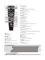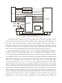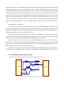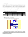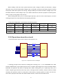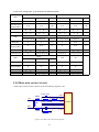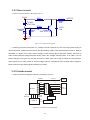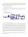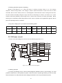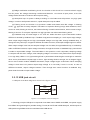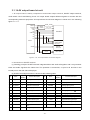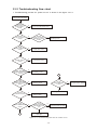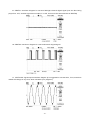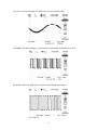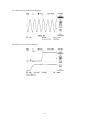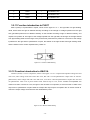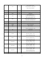
1
DV718SI
service manual
Catalog
Chapter One About Maintenance
1.1 Safety precautions
1
1
1.1.1 Power supply
1
1.1.2 Precautions for antistatic
1
1.1.3 Precautions for laser head
1
1.1.4 About placement position
2
1.2 Maintenance method
2
1.2.1 Visualized method
2
1.2.2 Electric resistance method
2
1.2.3 Voltage method
2
1.2.4 Current method
2
1.2.5 Cutting method
2
1.2.6 Element substitution method
3
1.2.7 Comparison method
3
1.3 Required device for maintenance
Chapter Two Functions and Operation Instructions
3
4
2.1 Features
4
2.2 Control Button Locations and Explanations
5
2.2.1 Front Panel Illustration
5
2.2.2 Rear Panel Illustration
5
2.2.3 LED Display Window Illustration
5
2.2.4 Remote Control Illustration
5
2.3 Accessories
6
2.4 FUNCTION SETUP
6
2.4.1 Function Setup
6
2.4.2 Language
7
2.4.3 Image
7
2.4.4 Sound
8
2.4.5 Playback
9
2.4.6 Karaoke
9
2.4.7 Preference
10
2.4.8 Parental control
10
2.4.9 Initial setup
10
2.4.10 Rest to defaults
10
2.4.11 Exit
10
2.5 Specifications
Chapter Three Principle and Servicing
Section One Principle of the Player
10
13
13
3.1.1 Functions and features
13
3.1.2 Block diagram of the player
13
3.1.3 Introduction to IC of the player
15
Section Two Unit Circuit Principle
16
3.2.1 Introduction to laser head
16
3.2.2 Servo circuit
17
3.2.3 CD/DVD conversion circuit
19
3.2.4 Laser power control circuit
20
3.2.5 Open/close door drive circuit
21
3.2.6 Main axis control circuit
22
3.2.7 Decode circuit
24
3.2.8 Video circuit
25
3.2.9 Reset circuit
26
3.2.10 Audio circuit
26
3.2.11 Mute circuit
27
3.2.12 Power circuit
28
3.1.13 USB jack circuit
29
3.2.14 AV output board circuit
30
3.2.15 Panel control circuit
31
3.2.16 HDMI circuit
32
Section Three Servicing Cases
34
3.3.1 Servicing cases
34
3.3.2 Troubleshooting flow chart
38
Section Four Waveform diagram
45
Section Five Function Introduction to IC
53
3.5.1 function introduction to MT1389HD
53
3.5.2 function introduction to AT24C02
69
3.5.3 function introduction to Cs5340
70
3.5.4 function introduction to 74HCU04
71
3.5.5 function introduction to FLASH
71
3.5.6 function introduction to SDRAM
72
3.5.7 function introduction to 4580
73
3.5.8 function introduction to D5954
74
3.5.9 function introduction to Pt6961
75
3.5.10 function introduction to VIPer22ADIP
77
3.5.11 function introduction to P H817
78
3.5.12 function introduction to LM431A
78
3.5.13 Function introduction to 455 8
79
3.5.14 Function introduction to TDA1308
80
3.5.15 Function introduction to MT1392E
81
Chapter Four Disassembly and Assembly Process
85
Chapter Cinque PCB board & Circuit diagram
86
Section One PCB board
86
Section Two circuit diagram
97
Chapter six BOM List
106
Chapter One About Maintenance
1.1 Safety precautions
1.1.1 Power supply
When maintenance personnel are repairing DVD players, he should pay special attention to
the
power board with 220V AC and 330V DC which will cause hurt and damage to persons!
1.1.2 Precautions for antistatic
Movement and friction will both bring static electricity which causes serious damages to integrated
IC. Though static charge is little, when a limited quantity of electric charge is added to largescaleintegrated IC, as the capacitance is very small in the meantime, now the integrated IC is very much
easy to be struck through by static electricity or the performance will decrease. Thus static electricity
prevention is of extraordinary importance. The following are several measures to prevent static
electricity:
1. Use a piece of electric conduction metal with the length of about 2 metres to insert into the earth,
and Fetch the lead wire from the top of the surplus metal and connect to the required static electricity
device. The length and depth of the metal embedded under the earth should be determined according to
the wettability of the local soil. For humid places, it may be shorter, and longer and deeper for dry places.
If possible, it can be distributed and layed in terms of “#” shape.
2. On operating table-board, the antistatic table cushion should be covered and grounded.
3. All devices and equipments should be placed on the antistatic table cushion and grounded.
4. Maintenance personnel should wear antistatic wrist ring which should be grounded.
5. Places around the operating position should also be covered with electric conduction cushion or
Painted with antistatic paint.
1.1.3 Precautions for laser head
1. Do not stare at laser head directly, for laser emission will occur when laser head is working, which
will Hurt your eyes!
2. Do not use wiping water or alcohol to clean laser head, and you may use cotton swab.
-1-
1.1.4 About placement position
1. Never place DVD player in positions with high temperature and humidity.
2. Avoid placing near high magnetic fields, such as loudspeaker or magnet.
3. Positions for placement should be stable and secure.
1.2 Maintenance method
1.2.1 Visualized method
Directly view whether abnormalities of collision, lack of element, joint welding, shedding welding,
rosin joint, copper foil turning up, lead wire disconnection and elements burning up among pins of
elements appear. Check power supply of the machine and then use hands to touch the casing of part of
elements and check whether they are hot to judge the trouble spot. You should pay more attention when
using this method to check in high voltage parts.
1.2.2 Electric resistance method
Set the multimeter in resistance position and test whether the numerical value of resistance of each
point in the circuit has difference from the normal value to judge the trouble spot. But in the circuit the
tested numerical value of resistance is not accurate, and the tested numerical value of integrated IC's
pins can only be used for reference, so the elements should be broken down for test.
1.2.3 Voltage method
Voltage method is relatively convenient, quick and accurate. Set the multimeter in voltage position
and test power supply voltage of the player and voltage of a certain point to judge the trouble spot
according to the tested voltage variation.
1.2.4 Current method
Set the multimeter in current position and test current of the player of a certain point to judge the
trouble spot. But when testing in current method, the multimeter should be series connected in the
circuit, which makes this method too trivial and troublesome, so it is less frequently used in reality.
1.2.5 Cutting method
Cutting method should be combined with electric resistance method and voltage method to use.
This method is mainly used in phenomena of short circuit and current leakage of the circuit. When
cutting the input terminal voltage of a certain level, if voltage of the player rises again, it means that the
trouble lies in this level.
-2-
1.2.6 Element substitution method
When some elements cannot be judged good or bad, substitution method may de adopted directly.
1.2.7 Comparison method
A same good PC board is usually used to test the correct voltage and waveform. Compared these
data with those tested through fault PC board, the cause of troubles may be found.
Through the above maintenance method, theoretical knowledge and maintenance experience, all
difficulties and troubles will be readily solved.
1.3 Required device for maintenance
Digital oscillograph ( 100MHE)
TV set
SMD rework station
Multimeter
Soldering iron
Pointed-month pincers
Cutting nippers
Forceps
Electric screw driver
Terminals connecting cord
Headphone
Microphone
-3-
Chapter Two
Functions and Operation Instructions
2.1 Features
This player has employed the new generation DV decode chip with built-in Dolby Digital decoder
which willbring you to a brand-new AV entertainments world. The 2-laser super error-correction
mechanism supports CD-R.
Brand-new AV Effects
#Compatible with DivX, MPEG4 discs to produce wonderful pictures.
#108MHz/12bit video DAC, with more vivid and brilliant pictures.
#Progressive-scan video outputs to eliminate the flickers hardly overcome by interlacing scan and
therefore your eyesight will be well-protected. At the same time, the pictures definition Is sharply
enhanced and the pictures will be finer, smoother and stabler
#Brightness, chroma and contrast adjustment functions to render your eyes more comfortable.
#Digital echo Karaoke to enable your singing easier.
#Composite Video, S-Video and Component Video outputs.
#Bullt-In Dolby Digital decoder, separate 5.1Ch Outputs.
#Dolby output for 2channel(DOWNMIX)
#DVD-Audio decoding output to reproduce original and realistic sound effects.
High Quality Digital Audio
#Optical and coaxial outputs for Digital audio.
#DTS,Dobly Digital, PCM Digital audio outputs to satisfy the fans’ss acoustic requirements.
Many Convenient Features
#Screen saver protects your TV set carefully.
#The novel Mp3 playback window GUI provides you a new way to appreciate Mp3 music.
#Multi-angle playback function makes it possible for you to view a scene from different camera angles.
#It’s possible to select the desired beginning, development and ending of a story.
#Direct entry into desired scenes(title/chapter/track search).
#Zooming function to zoom up any playing picture.
#Capable of playing PAL/NTSC discs.
#Multiple aspect ratios to fit TV sets of various screen ratios.
#Parental lock function to prevent children from watching unsuitable discs.
#Multiple dubbing languages and subtitle languages bring you the best entertainment status all the time.
Super Compatibility with super VCD, VCD, CD , CD-R , MP3,HDCD,KODAK PICTURE CD etc.
NOTE: DivX version is still upgrading continuously and the latest version of this unit is DivX 5.1.
Some discs labelled with MPEG4 on the market actually are others, with which are uncompatible .
Please take care when buying discs.
-4-
2.2 Control Button Locations and Explanations
2.2.1 Front Panel Illustration
2
3
5
4
4
6
7
8
9 10
1
Slot flap for USB
6
IR SENSOR
2
MIC jack
7
Display window
3
Headphone jack
8
OPEN/CLOSE button
4
POWER switch
9
PLAY/PAUSE button
5
Disc tray
10
STOP button
2.2.2 Rear Panel Illustration
2
3
4
5
6
7
8
9
1
Mixed Audio out jack
2
5.1CH Audio Out jack
6
Video Component /Y Pb Pr out jacks
3
S-Video
7
Digital Audio Coaxial Out jack
4
Video Out jack
8
Digital Audio Optical Out jack
5
HDMI Out jack
9
SCART out jack
2.2.3 LED Display Window Illustration
1
Playback time
2.2.4 Remote Control Illustration
1
[
] Button
4
Open or close the disc tray.
2
3
DISP Button
Display or hide disc information.
LANG Button
5
NUMBER Buttons
Change the audio language or audio channel.
6
BROWSE Buttons
MEMORY Button
switch new user interface.
Save the playing point or jump to the saved point .
7
-5-
CURSOR Buttons
8
1
15
16
17
18
2
3
4
ETUP Button
Function Setup.
9
[
]
Button
Open/close the virtual keyboard function.
5
10
KARAOKE Button
Karaoke operation menu.
6
19
7
20
11
21
22
23
24
25
26
11
12
13
14
USB
DVD
]
Button
Fast backward play.
12
8
9
10
[
[
] Button
Skip backward.
13
PEPEAT Button
Repeat play.
14
A-B Button
Repeat the select.
27
15
[
] Button
Press once to stand by, Press twice to play.
28
16
29
SUBT Button
Change subtitle language.
17
HDMI Button
Switch output mode of HDMI.
18
Q-PLAY Button
Skip the advertisement/warning and play the DVD directly.
19
25
[
Display DVD menu or open/close PBC.
] Button
20
OK Button
] Button
21
Cancel Button
Skip forward.
22
ZOOM Button
Stop playback.
26
MENU Button
[
Zoom in/out the displayed frame.
27 USB DVD Button
28 VOL +/- Button
23
Press once to mute, twice to unmate.
]
Button
Play or pause playback.
Increase/decrease volume level.
29 MUTE Button
[
24
[
] Button
Fast backward play.
2.3 Accessories
1PCS
1PCS
2PCS
1PCS
1PCS
1PCS
AUDIO/VIDEO CORD
REMOTE CONTROL
AAA SIZE BATTERIES
WARRANTY CARD
USER MANUAL
KARAOKE DISC
2.4 FUNCTION SETUP
2.4.1 Function Setup
-6-
1.Press the [SETUP] button and the screen
displays the selection menu of function setup.
Setup menu
Russian
DVD menu
English
Ukrainian
Soundtrack
Language
Setup menu
Image
DVD menu
Sound
Soundtrack
Playback
Subtitle
Sbutitles
1.Setup menu: This item is used to set the
prompts language on the screen.
#Optional setting: Russian, English, Ukrainian.
#Default: English.
2.DVD menu: To set the preference disc menu
lang when playing.
#Optional setting: Russian, English, Estonian,
Latvian, Kazakh, Romanian, Byelorussian,
Ukrainian, Chinese, Others.
#Default: English.
3.Sountrack:To set the preference audio
language when playing.
#Optional setting: Russian, English, Estonian,
Latvian, Kazakh, Romanian, Byelorussian,
Ukrainian, Chinese, Others.
#Default: English.
4.Subtitles: To set the preference subtitle
language when playing.
#Optional setting: Off, Russian, English,
Estonian,Latvian, Kazakh, Romanian,
Byelorussian, Ukrainian, Chinese, Others.
#Default: Off.
Off
Karaoke
Preference
Parental control
Initial setup
Reset to defaults
Exit
2.Press the [CURSOR] button to select the menu
to be entered and press the [OK] or button to
confirm. Or press the [CURSOR] button to
Exit item and then press the [OK] button to exit .
3.Press [UP/DOWN] arrow to select the desired
item you want to set and press [OK].
For example, press [UP/DOWN] arrows to
select IMAGE and press [OK]. The Image setting
page appears on the screen.
TV system
TV scan mode
AUTO
IS
Video out.
Com.
TV format
16:9
Sharpness
Gamma
PAL
NTSC
M
Brightness
0
0
Hue
0
Saturation
AUTO
Off
Contrast
2.4.3 Image
TV system
TV scan mode
0
TV scan mode
TV format
16:9
Sharpness
Gamma
M
Off
Brightness
0
Contrast
0
Hue
0
Saturation
0
Com.
16:9
AUTO
PAL
NTSC
M
Off
Brightness
0
Contrast
0
Hue
0
Saturation
0
1.TV system: This item is used to the video
output system of this unit.
#Optional setting: Auto, PAL, NTSC.
#Default: AUTO.
2.TV scan mode: To set Progressive scan,
Interlaced scan mode.
#Optional settings: Progressive , Interlaced.
#Default: Interlaced.
3.Video output: To set the types of SCART out
connector.
#Optional setting: Component , SCART.
#Default: Component.
#When using RGB outputs from the SCART
interface,please select RGB. Other wise ,
please select Com-ponent.
IS
Com.
IS
Video out.
Gamma
AUTO
Video out.
AUTO
TV format
Sharpness
4.Press [UP/DOWN] arrow to select the
SHARPNESS item. Press [OK] to confirm it.
And then press [UP/DOWN] arrow to select
the desired valus.For example: Press[
UP/DOWN] arrow to select “Medium” ,then
press [OK], the TV screen display.
TV system
Off
High
Medium
Low
5. Press [LEFT] button if you want to return to
the previous setup page.
6.Press [SETUP ]to exit the setup menu.
2.4.2 Language
-7-
4.TV format: To set the aspect ratio of this
player’s output image.
#Optional setting: 4:3 Pan-scan, 16:9 letterb.,
16:9 TV, Wide/SQZ.
#Default: 16:9 TV.
5.Sharpness:Used to set the sharpness of video
outputs.
#Optional setting: High, Medium, Low.
#Default: Medium.
6.Gamma emendation:This item is used to setup
the Gamma value of video output.
#Optional setting: High, Medium, Low, Off.
#Default: Off.
7.Brightness:Used to set the brightness of video
outputs.
8.Contrast:Used to set the contrast of video
outputs.
9.Hue: Used to set the hue of video outputs.
10.Saturation: Used to set the saturation of video
outputs.
#Brightness, contrast, hue and saturation
adjusting means:
A.Press [UP/DOWN] arrow in the video setup
menu to select the desired item you want to
adjust. Press [OK] or [RIGHT] button to enter
the item's adju-stment.
B.Press [UP/DOWN] arrow to adjust the setting
value.
#Optional setting: L+R, L, R.
#Default: L+R.
C.Surr. Mix: To set output means of the surround
left and right audio when playing a stereo disc.
#Optional setting: Off, sum, Virt.Surr.
#Default: Off.
D.Low band: select the channel that you desire
to output low frequency signal.
#Optional setting: Front F, Center C, Surround Sr,
Subwoofer SW.
#Default: Front F, Subwoofer SW.
E.Channels: To set volume of each individual
channel.
a. Press [UP/DOWN] navigation keys to select
CHANNEL TRIM, then press the [OK] or
[RIGHT]navigation key to select ENTER
SETUP PAGE as shown in the TV screen:
FRONT
Volume L
16
Mixer...
Configuration
Stereo mix
HDMI Audio
Tuning
On
St.
L+R
Surr. Mix
sum
Low band
FSW
Channels
Delays
PRO Logic II
Off
1.Mixer...
Configuration
Stereo mix
St.
L+R
Surr. Mix
sum
Low band
FSW.
16 16
surround
l
r
Center SW
16
16
16
16
b.Press [LEFT/RIGHT] navigation keys to select
the desired channel to adjust.
c. Press [UP/DOWN] navigation keys to raise or
lower volume of the channel.
d. Press [OK] or [LEFT] to return to the Mix..
setup page.
F. Delays: To set delay time of the Center/
Surround/ Subwoofer Speaker.
A. Press [UP/DOWN] navigation keys to select
Delays in Channels item, then press [OK] or
[RIGHT] navigation key select ENTER SETUP
PAGE as shown in the TV screen.
2.4.4 Sound
Digital output
R
Stereo
5.1
Channels
Subwoofer
Delays
PRO Logic II
AUTO
A. Configuration: To set this player’s DOWNMIX
mode to change multi-channel audio into two
channel audio.
#Optional setting: Stereo, 5.1.
#Default: Stereo.
B. Stereo mix: To set the output means of the left
or right audio when playing a Dolby disc with
separate two-channel audio.
0cm
Center
0cm
LS/RS
180cm
b.Press [UP/DOWN] navigation keys to Select
the desired item oup Press [OK] or [RIGHT]
button to enter setting.
c. Press [UP/DOWN] navigation keys to raise or
lower volume.
D.Press [OK] or [LEFT] to return to the Delays in
channels setting page.
-8-
G. PRO Logic II: To set PRO Logic II to ON or
OFF. If the TITLE does not support this
function, we recommend that you set this item
to AUTO because it would become worse if the
processing effects were added forcibly.
#Optional setting: AUTO, On, Off .
#Default: AUTO.
2. Digital output: select to set the format and
stream form of digital audio output.
A. SPDIF format:3Optional setting: RAW format,
SPDIF/PCM.
#Default: RAW format.
B. LPCM
#Optional setting: 48 kHz 16bit , 96 Khz 24bit,
192kHz 24bit
#Default: 48 kHz 16bit.
NOTE
If HDMI Audio is set in ON, this item is not
adjustable.
3. HDMI Audio: This item is to set whether
the HDMI Audio output is allowed.
#Optional settings: SPDIF Multi Channel off.
#Default: Multi.
4. Tuning:
A. Max volume: set the maximum volume.
B.Equalizer: To set Equalizer modes.
#Optional setting: Off, Rock, Pop, Live, Dance,
Techno, Classic, Soft.
#Default: Off.
C. Echo: To set different sound field effects.
#Optional setting: Off, Concert, Living room, Hall,
Bathroom, Cave, Arena, Church.
#Default: Off.
D.Tone balance: to set the tone level to match
your diapason when you're singing
#Method to adjust tone control:
a.Press [UP/ DOWN] cursor buttons to select
"tone" item in Audio Setting page, and then
press [OK] or [RIGHT] button to enter
Adjustment Menu.
b. Press [UP/DOWN] cursor button to adjust
setting value.
c. Press [OK] or [LEFT] button to return to Audio
Setting page after adjustments are done.
skipped to play the movie directly.
Advertisemenu
#Optional setting: Yes, NO
#Default: Number
2.VCD/SVCD: To set the PBC status.
#When playing Super VCD or VCD2.0 discs, if
the PCB is ON, the menu image displays.
#Optional setting: On, Off.
#Default: On.
3.Files:data disc may probably includes Mp3,
JPEG and MPG format files in which you may
select DVD player to read the file type.
#Optional setting: Audio, Picture, Video.
#Default: Audio, Picture, Video.
4. Repeat : select the repeat playback mode.
#Optional setting: Off, Single, all.
#Default: Off.
2.4.6 Karaoke
Microphone
Kar. help
Advertisemenu
Repeat
No ast.
Off
Volume
5
Echo
5
Microphone
Kar. help
On
No ast
Volume
4
Echo
4
4.Echo:
A.In microphone setup page, press [UP/DOWN]
cursor to select “Echo” item, and then press
[OK] button to enter the adjustment menu.
B.Press [UP/DOWN] cursor to adjust the setup
value.
C.After the adjustment finishes, press [OK]
button to return to microphone setup page.
No
VCD/SVCD
Files
On
1.Microphone: switch on or off microphone.
#Optional setting: On, Off.
#Default: Off.
2.Kar. help: select accompany singing means.
#Optional setting: Channels L, Channels R,
Channels No ast, Channels No voc.
#Default: Channels No ast.
3.Volume:
A.In microphone setup page, press [UP/DOWN]
cursor to select “Volume” item, and then press
[OK] button to enter the adjustment menu.
B.Press [UP/DOWN] cursor to adjust the setup
value.
C.After adjustment finishes, press [OK] button
to return to microphone setup page.
2.4.5 Playback
DVD
On
A. P. V
Off
1. DVD:set whether information of advertisement
and warnings at the beginning of DVD disc is
-9-
Microphone
Kar. help
#Default: 7890.
On
No ast.
Volume
5
Echo
4
Old password
New password
2.4.7 Preference
Verify
Gr. equalizer
Off
Screen saver
On
Off
2.4.9 Initial setup
1.Backlight:This item is used set color of led on
the front panel.
#Optional setting: On, Off.
#Default: On.
2.Gr. equalizer: This item is used to set wether
the Dynamic Spectrum is allowed.
#Optional setting: On, Off.
#Default: Off.
#Dynamic Spectrum display is invalid in Data
disc DVD AUDIO playback.
3.Screen saver: Open or close the screen saver
function.
#Optional setting: On, Off.
#Default: On.
Auto
PAL
NTSC
Press [UP/DOWN] arrow to select the
desired option and Press [OK] button to confirm
it.
NOTE
In this setup state, you may not press [LEFT]
button to return to the previous menu.
2.4.10 Rest to defaults
Load factory settings
2.4.8 Parental control
OK
any
G
Set password
Any
Cancel
Reset to defaults: To restore all settings to
the default value except for the parental control
and password settings.
Kid
Allowed..
Cancel
OK
On
Backlight
PG
2.4.11 Exit
PG-13
PGR
R
Language
NC-17
Image
Sound
1.Allowed..: To set the parental control ratings to
prevent children from watching the restricted
contents.( In case the disc supports this
function.)
#Optional setting: any, Kid, G, PG, PG-13, PGR,
R ,NC-17.
#Default: any.
2.Set password: To set four digit password to
enable you to change the parental control
ratings.
Playback
Karaoke
Preference
Parental control
Initial setup
Reset to defaults
Exit
Press [UP/DOWN] arrow to select the Exit
item. Press [OK] button to exit the setup menu.
2.5 Specifications
Playerable discs
DVD-Video, Super VCD, VCD, DivX 3.11, DivX 4,DivX 5, Divx Pro, XviD, CD-DA,
CD+G, DVD-Audio,HDCD, MP3, WMA, Kodak Pictur e CD, JPEG
Inputs
MIC input
Outputs
Audio outputs
Analog audio output:
Digital audio output:
- 10 -
Stereo, output 5.1CH
Coaxial,Opcical
Playerable discs
DVD-Video, Super VCD, VCD, DivX 3.11, DivX 4,DivX 5, Divx Pro, XviD, CD-DA,
CD+G, DVD-Audio,HDCD, MP3, WMA, Kodak Pictur e CD, JPEG
Inputs
MIC input
Outputs
Audio outputs
Analog audio output:
Digital audio output:
Video outputs
Composite, S-Video, component Y Cb Cr, progressive scan
output Y Pb Pr, RGB/SCART
Outputs
Stereo, output 5.1CH
Coaxial,Opcical
Headphones output
Video amplitude
S-Video amplitude
Component Video amplitude
1.0Vp-p(75 )
Y:1.0Vp-p(75 ) C:0.286Vp-p(75
Y:1.0Vp-p(75 )
Cb/Cr:0.7Vp-p(75 )
Audio characteristions
Frequency response
Slgnal-to-noise ratio
THD
20~20KHz(±1 dB)
>100(dB)
<0.01%
Operating voltage
~110V-250V, 50/60 Hz
Power consumption
14W
General Specifications
Dimensions:
Mass:
Operating Temperature
5~35
Operating Humidity
15~75%(no condensation)
Video Characteristics
380mm
1.86kg
250mm
)
41.5mm
#Design and specifications are subject to change without notice.
#We do not guarantee that all discs can be played smoothly due to the disc quality, disc recording quality
and recording format.
Play erable disc s
DVD-Video, Super V CD, VCD, DivX 3.11, DivX 4,DivX 5, Divx Pro, XviD, CD-DA ,
CD+G, HDCD, MP 3, W MA, Kodak Pic ture, JPEG
Input
MIC input
Output
Audio outputs
Analog audio out put:
Digital audio output :
S tereo, out put 5.1CH
Coaxial, Opt ical
Video outputs
Composit e, S-V ideo, c omponent Y Cb Cr, progressive scan
output Y Pb Pr, RGB/SCART
Headphones output
Video Characteris tic s
Video ampl itude
S-Video amplit ude
Component Video amplitude
Audio c haracteristions
Frequency response
Slgnal-t o-noise ratio
THD
Operating voltage
~110-250V, 50/60Hz
1. 0Vp-p(75 )
Y:1. 0Vp-p(75 ), C:0. 286Vp-p(75 )
Y: 1.0Vp-p(75 ), Cb/Cr:0. 7Vp-p(75 )
20~20KHz (±1 dB)
>100(dB)
<0.01%
- 11 -
Power cons umption
14W
General Spec ificat ions
Dimensi ons:
Mass:
Operating Temperature
5~35
Operating Humi dity
15~75%(no c ondensation)
380mm
2kg
258mm
41.5mm
#Design and specifications are subject to change without notice.
#We so not guarantee that all discs can be played smoothly due to the disc quality, disc recording quality
and recording format.
- 12 -
Chapter Three Principle and Servicing
Section One Principle of the Player
3.1.1 Functions and features
This player adopts new generation DVD decode chip, with built-in Dolby decoder, which creates
vivid surround sound effect to bring you to taste cinema effect. It has the following features:
Progressive scanning output produces steadier and clearer pictures with flickering.
HDMI jack.
5.1CH output.
Composite video, S-video and component video output.
Digital picture adjustment to the sharpness, brightness, contrast, chroma and saturation os
picture, gamma correction.
Built-in Dolby digital decoder.
Karaoke function.
Headphone output function.
USB jack.
Compatible with DIVX, MPEG4 format movie.
3.1.2 Block diagram of the player
Its internal structure is mainly composed of decode & servo board, HDMI high definition board,
input/output board, power board and loader components. Block diagram of the player is shown in the
figure 3.1.2.1, except for power board, other signal flow are all shown in the figure. Main function of
loader is to read disc information and transmit to Mt1389, Mt1389 fulfills servo function through D5954
on decode board and other subsidiary circuit to ensure the normal working of loader. FLASH on decode
board is to save system program, SDRAM is to save program when machine is working and read sound
and picture information from disc to ensure smooth output. Main function of AV board is to output various
video signals.
- 13 -
Loader
CS5340
U203
IOA
LDO2
LDO1
SCL
SDA
INT0#
PWDN#
Y0
Y1
Y2
Y3
Y4
Y5
Y6
Y7
SLRCK
SL+
SP+
SP-
FOSO
LOUD+
M
IOA
STBY
U302
AM5888S
FMSO
DMSO
SBCLK
TRSO
SACLK
SDATA0
SDATA1
SDATA2
SDATA3
ASPDIF
TROPEN
LOUD-
TRCLOSE
TR_B1
REG01
TR_B2
REG02
Voltage
reduce
circuit
Voltage
reduce
circuit
VCC
3.3V
XI
XO
VCC
1.8V
SR
LFE
Cc
SY
SC
Video CVBS
filtering
clamping G/Y
B/U
R/V
HPD
HDMI SCL#
HDMI SDA#
U201
M
U209
U210
U211
YUV1
YUV2
YUV3
YUV4
YUV5
YUV6
TK+ TK- FC+ FC-
VIP4
Audio
Rt
amplifying
SL
audio
ASPDIF
MDI
DVD:A/B/C/D/RFO
CD:A/B/C/D/E/F
V20
TRIN
TROUT
LIMIT
SL-
Lt
AL
AR
ALS
ARS
SW
CTR
Mt1389HD
M
MIC
27M cock
SCL
SDA
EEPROM
U202 24C02
UREST
Reset
MT 1392
VR-DVD
Laser power
VR-CD control
FLASH16M
U214
AV output terminal
VR-DVD
CD/DVD
VR-CD
Switch
SDRAM 64M
U211
TX 0TX 0+
TX 1TX 1+
TX 2TX 2+
TXCTXC+
HPD
HDMI jack
- 14 -
Panel
USB
Figure 3.1.2.1 Block diagram of the player
Earphone
3.1.3 Introduction to IC of the player
Introduction to IC of the player is shown as in the following table:
PCB semi-finished
product name
Decode board
IC model
Location
Function
MT1389HD
U201
Decode chip
24C02
U202
EEPROM
CS5340
U203
HCU04
U205
Phase inverter
FLA SH
U207
16M FLASH
SDRA M
U208
64M SDRAM
4580
U209, U210, U211
Operational amplifier (audio amplifying)
D5954
U302
Servo driv e
PT6961
U401
Panel control IC
HS0038B3V
U402
Remote control rec eiver
VIPER22
U501
Power sw itch IC
PH817
U502
Photoelectric coupler
LM431A
U503
Precision voltage stabilizer
4558
U601
Operational amplifier (audio amplifying)
TDA1308
U603
Operational amplifier (headphone audio
amplify ing)
MT1392E
U701
HDMI control
TVS_RCLAMP0514M
U703, U704
Main panel
Power board
MIC board
High definition
board
- 15 -
Section Two Unit Circuit Principle
3.2.1 Introduction to laser head
1. Function introduction to laser head flat cable is shown as the following table:
Pin
Name
Signal flow
direction
DVD disc
CD disc
No disc
Function description
1
F-
Input loader
2.52
2.34
0.46
2
F+
Input loader
2.49
2.49
0.93
Focus error signal is added to two sides of
pick-up focus coil
3
T+
Input loader
2.53
2.51
0.94
4
T-
Input loader
2.58
2.51
0.93
5
C
Input MT1389
2.2
2.25
2.04
Disc data signal
6
D
Input MT1389
2.2
3.2
2.04
Disc data signal
7
IOA
Input MT1389
0.01
3.2
3.21
Disc identification signal, CD is 3.3V, DVD
is 0V
8
RF
Input MT1389
2.21
2.53
1.28
The sum of disc data signal
9
A
Input MT1389
2.17
2.22
2.04
Disc data signal
10
B
Input MT1389
2.19
2.27
2.04
Disc data signal
11
F
Input MT1389
2.07
2.44
2.03
Supplementary signal used in trace
12
GND
Ground
0.01
0.01
0
Grounding
13
V20
Input loader
2.04
2.06
2.03
Reference voltage
14
Vcc
Input loader
5.04
5.04
5.02
Supply voltage for loader
15
E
Input MT1389
2.06
2.45
2.03
Disc data signal
16
Blanking
haning in air
0.01
0
0
unused
17
VR-CD
Input loader
0.21
0.01
0
Through the handling inside loader, make
sure MD11 is 180mV when reading CD
18
VR-DVD
Input loader
0.01
0.2
0
Through the handling inside loader, make
sure MD11 is 180mV when reading DVD
19
LD-CD
Input loader
0.09
2.1
0
CD laser power control signal
20
MDII
Input MT1389
0.21
0.2
0
CD and DVD laser power monitoring signal
21
HFM
Input loader
5.04
5.04
5.02
High frequency overlapping signal produces
laser with different wave length inside
loader
- 16 -
Trace error signal is added to two sides of
pick-up trace coil
22
Blanking
unused
0.01
0.1
0
23
LD-DVD
Input loader
2.21
0.1
0
DVD laser power control signal
24
GND
unused
0.01
0.01
0
Grounding
Note: 1. When reading DVD, there are only A, B, C, D signals.
2. When reading CD, there are A, B, C, D, E, F signals.
3. RFO=A+B+C+D.
4. Focus error signal=(A+C)-(B+D) Trace error signal=E-F.
2. Working principle
(1) Laser tube: wave length of loader DVD laser diode is 650nm, wave length of CD laser diode is
790nm, the wave length which is within 370nm and 750nm is visible light, the laser in the course of
reading DVD disc is visible light, and that when reading CD disc is infrared light.
(2) Principle about laser head picks up signal: laser beam projects onto disc, when laser beam
focus projects onto disc vertically, laser beam will produce reflection, reach on light sensor through
reflection loop and converse into electronic signal through photoelectric cell. For the reflection loop
produced in non pit information area and pit information area in disc has difference and reflects into
different position of light sensor, photoelectric diode in different positions on light sensor will produce
different signals to process all signals on light sensor and then produce digital signals.
(3) Focus, trace coil: when laser head is reading signals normally, information side should be in the
focus of laser beam, because of factors of disc error, high speed rotation and machine error, it is
unavoidable that laser beam focus deviates from information face to produce phenomena of orbit boas
and refocusing. Focus , trace coil is added on loader to adjust laser beam to make it correctly focus in
information area.
(4) Formation of RF signal: when disc reading is normal, light sensor will have 160MV, vague and
eye pattern waveform which is added on A, B, C, D respectively, and output RF signal from FRO pin
after being overlapped by adder inside light sensor, the frequency when reading DVD disc is much
higher than that when reading CD disc, output amplitude is about 1.4V.
3.2.2 Servo circuit
1. Servo system of this player adopts SANYO 65 loader and MTK decode solution
(MT1389HD+FLASH (16M) +SDRAM (64M)), and its servo circuit is mainly composed of front end signal
processing, digital signal processing and digital servo processing, digital signal processing IC Mt1389
and drive circuit Am58888, in which Mt1389 is also the main part of decode circuit. Servo circuit block
diagram is shown in the figure 3.2.2.1:
- 17 -
IOA
Switch circuit
MD11
LDO2
LDO2
APC circuit
A B C D E F RFO
XS101
TK- 15
TK+
16
FC+
14
FC13
Feed
electric
machine
Main axis
electric
machine
SL+
17
SL-
1
23
26
4
FOSO
FMSO
TRSO
MT1389
DMSO
AM5888
18
SPSP+
12
Open/close
circuit
11
Main axis
control detect
circuit
Figure 3.2.2.1 Servo circuit block diagram
2. Working principle: after power on or close to proper position, loader laser head begins to reset;
after laser head reaches proper position, detect switch will give a signal to Mt1389, Mt1389 begins to
output focus, main axis and light emission signals, machine begins to rotate, laser head begins to
identify disc information and decide whether disc is CD or DVD according to disc information to facilitate
to output level from IOA pin to make disc switch circuit and laser head PD IC make the relevant control
action. At the same time, Mt1389 adjusts laser output power through laser power control circuit.
After loader reading disc information, A, B, C, D, E, F signals are formed through photo-electric
conversion and sent out to Mt1389 (DVD only has A, B, C, D signals), and then inputted from pin 2~11,
18, 19 of MT1389. After being amplified and processed by the pre-amplifier inside MT1389, now signals
are separated to two part s for processing inside Mt1389. One part, through addition inside Mt1389 and
amplifying and subtraction circuit, produces servo error signal, after being processed by digital servo
signal circuit, corresponding servo control signals form to output FOO, TRO, DMO, FMO digital
servoControl signals from pin 42, pin 41, pin 37, pin 38 of Mt1389 respectively, and FOSO, TRSO,
DMSO, FMSO, through integration circuit composed by resistor capacitor, and send to servo driver
circuit for amplification to bring along focus winding, trace winding, main axis electric machine and feed
electric machine after drive amplification. Among these, focus and trace servo are used to correct
objective position accurately; feed servo is used to bring along laser head to make radial large-scale
move which belongs to the preliminary adjustment to laser head position; and main axis servo is used to
control main axis electric machine to make it read signals in means of constant linear velocity and
bringAlong disc to rotate. After processing of amplification by VGA voltage control amplifier and
- 18 -
equalization Frequency compensation inside MT1389, another part of signals are changed into digital
signals through internal A/D converter. When loader is reading CD/VCD signals, these signals are
conducted EFM demodulation inside MT1389, and then outputted to latter stage for AV decoding after
finishing CIRC (Cross-Interleaved Reed-Solomon Code) error correction inside. When loader is reading
DVD signals, these signals are conducted ESM demodulation inside MT1389, and then sent to latter
stage for decoding after finishing RSPC error correction inside. Normal DVD player has a open/close
circuit to control the in and out of door to reach the purpose of coneying discs; PDVD adopts manual
open means and whether it is close to proper position can be checked by detect switch.
3. Explanation to servo terms
(1) FOO: when rotating, disc may probably move upwards or downwards slightly to make the focus
of laser emitted by laser head cannot justly fall on data pit of disc, so laser head is required to move
upwards or downwards to make focus aim at data pit justly. When laser head is moving upwards or
downwards, it means that pick-up is making focus acts.
(2) TRO: data information is saved in disc in form of tracks. When disc is rotating, trace deviation
will produce and now laser head is required to be adjusted. In this process, it is objective, but the entire
pick-up, that moves forwards or backwards, and the moving range is very small.
(3) FMO: similar to acts of trace, the acts of feed are larger than those of trace. Feed conducts a
large scale movement firstly, and then trace moves slightly in this range. Feed moves for a while, and
does not move for another while; but trace moves all the time. Feed is rough adjustment and trace is fine
and acts are obvious when pwer on and selecting tracks.
(4) DMO: it is the top that holds up disc. Its rotation speed decides that of disc. Its rotation is
generated by an individual DC electric machine, in which rotation speed of DVD is twice over that of CD.
3.2.3 CD/DVD conversion circuit
1. CD/DVD conversion circuit is shown as in the following figure 3.2.3.1:
R308
R309
100K
10K
R311
AVCC
IOA
10K
Q305
3904-S
XS301
R310
Q303
17
18
100K
Q304
2SK3018-S
2SK3018-S
Figure 3.2.3.1 CD/DVD conversion circuit diagram
- 19 -
MT1389E
2. Working principle
After loading disc in the player, IOA port of MT1389 is defaulted high level to make Q305 saturation
on and form loop together with CD laser power control circuit on CD. At the same time, IOA also goes to
loader PD IC to switch, disc begins to rotate, when servo management system recognizes that the disc
in player is not CD disc, IQA pin outputs low level to make Q305 cut off and make Q303 on, and form
loop together with DVD laser power control circuit on loader to perform disc reading acts. After disc tray
door opens, IOA keeps the state before opening disc tray door. If the player cannot recognize which disc
it is, IQA pin will switch continuously until reading disc or system judges that there is no disc.
Note: Q303 and Q304 are MOS tube
3. Key point voltage (unit: V) is shown as the following table:
Q305
State
Q303
Bas e
Collector C
electrode B
Em itter E
Q304
Grid
Drain
Source
electrode G electrode D electrode S
G
D
S
IOA
DVD disc
0
3.86
0
3.81
0.18
0
0
0
0
0
VCD disc
0.64
0.1
0
0
0
0
3.27
0.18
0
3.3
3.2.4 Laser power control circuit
1. Laser power control circuit is shown as in the following figure 3.2.4.1:
R301 4.7R
LDO-AV33
TC302
47uF/16V
LDO2
Q301
2SB1132-S
23
20/21
MD1
XS301
MT1389E
20
19
Q302
2SB1132-S
LDO1
TC303
47uF/16V
4.7R R302
LDO-AV33
Figure 3.2.4.1 Laser power control circuit diagram
2. Working principle:Pin 20/21 of MT1389 is laser power detect signal input pin, pin 21 is DVD laser
power strong/weak detect signal input pin, pin 23 is VCD laser power drive control output pin, pin 22 is
DVD laser power drive control output pin.
- 20 -
When reading VCD disc, laser power becomes weak, voltage of MDII pin decreases, voltage
decrease of pin 23 of MT1389 makes voltage of pin 19 of XS301 increase to reach the purpose of raising
laser power. When laser power is too strong, voltage of MDII pin increases to lead to voltage of pin 23 of
MT1389 increase to make voltage of pin 19 of XS301 decrease to reach the purpose of reducing laser
power to form an auto power control circuit.
When reading DVD disc, pin 21 is detect signal input pin, pin 22 is drive control input pin, and the
working principle is the same with that when playing VCD disc.
3. Key point voltage (unit: V) is shown as the following table:
Location number
Read DVD disc
Read VCD disc
Location number
Read DVD disc
Read VCD disc
V103_E
2.9V
3.2V
V104_B
3.2V
2.2V
V103_B
2.2V
3.2V
V104_E
3.2V
2.9V
V103_C
2.2V
0
MT1389_20
0.2V
0.2V
V104_C
0
2.2V
3.2.5 Open/close door drive circuit
1. Open/close door drive circuit is shown in the figure 3.2.5.1:
R203 27K
TRSO
FC+
FCSPSP+
LOAD+
LOADTKTK+
SL+
SL-
STBY
V1P4
AM5888S
R202 15K
FMSO
MT1389
TRCLOSE
TROPEN
DMSO
R314
FOSO
10K
10K
R204 27K
R201
Figure 3.2.5.1 Open/close drive circuit diagram
2. Working principle: when machine is reading disc normally, pin 6, 7, 9, 10 of AM5888S is 0V. After
pressing OPEN button, pin 6 inputs high level, pin 10 LOAD+ outputs high level, electric machine rotates
positively and performs the action of opening door. When closing door, pin 7 inputs high level, pin 9
LOAD- outputs high level and forms loop to pin 9 through electric machine, electric machine rotates
reversely and performs action of closing door. After closing to proper position, all pins are low level.
Servo drive principle is the same with that of D5954 solution, so we will not introduce here.
- 21 -
3. Key point voltage (unit: V) is shown as the following table:
Q306
Q307
State
Base electrode B
Collector C
Em ittor E
Base electrode B
Collector C
Em ittor E
Read disc
5.06
5
5.06
5.01
5.03
5.06
Open disc tray to
proper position
4.79
4.77
5.06
4.77
4.79
5.06
Open disc tray
4.74 5.05 4.74
4.76 0.2 4.76
5.06
4.76 4.33 4.76 4.76 5.02 4.76
5.06
Close dis c tray 4.74 4.33 4.74 4.76 5.05 4.76
5.06
4.76 5.03 4.76
5.06
Q308
4.79 0.2 4.79
Q309
State
Base electrode B
Collector C
Em ittor E
Base electrode B
Collector C
Em ittor E
Read disc
0
5
0
0
5.03
0
Open disc tray to
proper position
0
4.77
0
0
4.79
0
4.76 0.2 4.76
0
0
4.79 5.02 4.79
0
4.76 5.05 4.76
0
4.79 0.2 4.79
0
Open disc tray
0
Close dis c tray
0.93 0
0
0
0.93 0
Q310
State
OUT
IN
0
0
0
0
0
0
0
0
0
Base electrode B
Collector C
Em ittor E
Read disc
0
0
Open disc tray to
proper position
0
Open disc tray
Close dis c tray
0
0.63 0
0
0
0.93 0
0
0
3.12 0
0
3.2.6 Main axis control circuit
1. Main axis control circuit is shown as in the following figure 3.2.6.1:
C307 222
SP-
R320
150K
R321
1R
SPL-
OPO
R318 0R ADIN
R317 680K
OP- MT1389
C308 222
OP+
V1P4
R319
150K
R322 680K
Figure 3.2.6.1 Main axis control circuit diagram
- 22 -
0
0
3.12 0
2. Function: disc is always in high speed rotation in the course of disc reading, when you need to
open the door to change disc, MT1389 stops the positive direction drive signal which is given to main
axis drive circuit, for the function of inertia disc is still rotating. If disc out order is performed at this time,
disc will be abrasively damaged. Therefore, machine must be baking to main axis, that whether disc has
stopped rotating and whether disc is reversing, decode chip of the machine cannot recognize. So a main
axis control circuit is added to make decode chip can effective monitor that whether disc has stopped
rotating.
3. Working principle: MT1389 has a comparator inside composed of operational amplifier, in which
OP+ is the in-phase input end of operational amplifier, OP- is reverse input end, OPO is output end,
when playing disc normally, for electric machine is positive direction rotating, voltage of OP+ is higher
than that of OP-, voltage of OPO is more than 1.4V. When disc out is needed, main axis drive signal
stops, for electric machine is permanent magnetic, when in rotating, induced electromotive force
produces in two ends to give to decode chip through R320, R319 sampling to make OPO output less
than 1.4V voltage and transmit to input pin of MT1389 ADIN through R318. When ADIN is high level,
main axis drive output end has not any drive signal output, when ADIN is low level, MT1389 outputs a
reversing drive signal to main axis drive circuit to make main axis electric machine speed down. Thus
circular working goes on until main axis stops rotating. PDVD is manual disc out means, so after disc out,
disc is still rotating, but will stop very son.
4. Key point voltage (unit: V) is shown as the following table:
Key point
Position
Normal w orking voltage (V)
Volateg change w hen disc out ( V)
SP+
Pin 11 of D5954, pin 5 of XS307
3.79
3.79 0.70 1.80
SP-
Pin 2 of D5954, pin 6 of XS307
1.38
1.38 3.40 1.80
OP+
Pin 36 of MT1389
1.38
1.38 3.10 1.80
OP-
Pin 35 of MT1389
1.53
1.53 3.08 1.98
OPO
Pin 34 of MT1389
2.44
2.44 0.40 2.50
ADIN
Pin 47 of MT1389
2.44
2.41 0.41 2.44
DMSO
Pin 5 of D5954
1.42
1.42
Pin 30 of MT1389
1.41
1.41
VIP4
- 23 -
3.2.7 Decode circuit
1. Decode circuit block diagram is shown as in the following figure 3.2.7.1:
PWR
SDCLK
PRD
SDCKE
DCS
PCE
DRAS
MT 1389
A0~A20
SWE
SDRAM
FLASH
DQM0
AD0~AD7
DQM1
DQ0~DQ15
URST
MA0~MA11
SDA
SCL
Reset
circuit
EEPROM
24C02
V18
Clock
27M
1.8V
voltage
regulating
U206
Figure 3.2.7.1 Decode circuit block diagram
2. Working principle: this decode circuit is mainly composed of MT1389, SDRAM and FLASH.
Working condition of decode circuit has:
(1) Reset: refer to reset circuit working principle for details.
(2) Clock: this system adopts 27M external clock input, and produces clock signal required by
system inside through internal frequency doubling circuit.
(3) Power: decode chip adopts twp groups power supply of 3.3V and 1.8V, in which 1.8V mainly
supply power for internal logic control circuit and we call it core voltage.
After power on, reset circuit performs reset to MT1389 built-in CPU (8032) and FLASH, decode chip
outputs reset signal at the same time and performs reset to other circuit. After system reset, it firstly
sends out read signal to FLASH to read out in formation saved in FLASH, the machine displays poweron picture, servo system begins to work to check whether machine closes door to proper position and
whether detect switch has been closed, if not, the door close action is performed. After detect switch of
door is closed, the machine begins to perform preparations of disc reading and performs panel display
at the same time of working.
Playback process: laser head picks up disc signal from disc, after servo system processing, then
send to decode circuit for decoding, signal after being decoded is saved in SDRAM for the moment.
When machine needs to replay signal, decode circuit calls information inside SDRAM to perform D/A
conversion and then output.
- 24 -
User information storage: information content set by user is saved inside EEPROM, if user does not
refresh or reset this information, it will saved in IC permanently.
Audio, video output circuit: at present, MT1389 all integrates video D/A converter, MT1389E inside
integrates audio D/A converter, manufactures select according to their own needs.
Please refer to
circuit principle diagram and audio circuit explanation for details.
3.2.8 Video circuit
1. Video signal flow chart diagram is shown as in the following figure 3.2.8.1:
191
189
MT1389
187
185
YUV1
YUV2
183
YUV5
182
YUV6
D209
L226
D210
L227
D211
AV
VIDEO-SY
S
VIDEO
Y1
VIDEO-SC
JK703
Pb
VIDEO-CVBS
YUV3
YUV4
L225
Pr
JK703
7
L701
D703
9 XS204
L702
D704
5
L703
D705
SCART
VIDEO-G/Y
VIDEO-B/U
VIDEO-R/V
Figure 3.2.8.1 Video signal flow chart
2. Working principle: MT1389E has built-in video D/A conversion circuit, video output has R/B/G
Y/Pb/Pr Y/Cb/Cr CVBS Y/C output mode, in which R/B/G Y/Pb/Pr Y/Cb/Cr Y/C cannot output at the
same time and need the switch through software. CVBS is a separate output mode, 4-path video signal
outputted by MT1389, through video filtering clamping, output to AV board.
Shown as in the figure 3.2.8.2, capacitor C287, C288 and inductor L214 compose a low-pass filter
to filter high frequency disturbance signal except useful signal; dual diode D211 composes a limiter
circuit, known from features of diode that the max amplitude of composite video signal CVBS cannot be
over 5.7, and the mix cannot be less than -0.7, thus the high voltage signal from TV set can be avoided
burning down the player.
5VV
L227
1.8uH
YUV3
R248
75R
VIDEO_CVBS
C287 C288
101
101
D211
1N4148*2
VGND
VGND
Figure 3.2.8.2 Video output circuit
- 25 -
3.2.9 Reset circuit
1. Reset circuit is shown in the figure 3.2.9.1:
DV33
R221
URST#
10K
R222
33R
TC208
47uF/10V
R220
1N4148
D201
R219
10K
1K
C272
104
Q201
2SC1815-YS
GND
Figure 3.2.9.1 Reset circuit diagram
2. Working principle: after power on, voltage of DV33 increases to 3.3V, main chip power supply is
normal, because voltage of DV33 cannot change suddenly, Q201 base electrode has current in, Q201 is
saturated on, URST is low level; DV33 charges TC208 through R219 and Q201 emitter electrode to
make TC208 cathode voltage decrease slowly. When this voltage reduces below 0.7V, Q201 cuts off,
URST changes into high level, and the process for URST from low to high is called low level effective
reset signals by us. After power off, DV33 voltage reduces, TC208 and DV33 voltage reduce together,
D201 performs surge discharge and clamping to Tc208.
3.2.10 Audio circuit
1. Audio circuit block diagram is shown in the figure 3.2.10.1:
ASPDIF
MT1389
SLRCK
AMDATA
CTR
ALS
227
AL
226
AR
224
ARS
223
SW
222
SACLK
SBCLK
CS5340
OK
R
LS
RS
C
SW
Mute circuit
MIC board
Figure 3.2.10.1 Audio circuit block diagram
- 26 -
AV
board
L
Audio amplifying
filtering
228
IEC958
Audio
terminal
2. Working principle: MT1389 has built-in DAC conversion circuit, which stimulates audio signals to
output from decode chip directly, through audio amplifying and filtering circuit, directly output audio
signals to audio terminal. Another path of L/R signal outputs to headphone circuit of MIC board for
processing and then output from headphone.
3. External Karaoke input and output
Trough CS5340 A/D conversion circuit, MIC signals switches to digital audio signals to input to
decode chip for echo and volume processing and then output together with audio signals L/R to fulfill the
purpose of Karaoke.
3.2.11 Mute circuit
1. Mute circuit is shown in the figure 3.2.11.1:
R2103
1K
+9V
DV33
VMUTE
R2107
10K
R2101
100K
Q213
1015
MUTE-1
D204
1N4148
DV33
Q214
1015
TC238
100uF/10V
R2104
1K
Q212
2SC1815-YS
Q211
1015
D203
1N4148
R2106
10K
TC235
100uF/10V
AGND
AGND
-9V
R2108
10K
R2105
10K
R2109
10K
Figure 3.2.11.1 Mute circuit
2. Working principle of quieting circuit
When the player is playing normally, shown in the figure 2.11.1, chip outputs analog audio signals
and a low level signal at the same time to VMUTE to make Q211 on, voltage of Q211B electrode is about
2.7V, voltage of Q211 collector electrode is about 3.3V, so Q212 is also on, voltage of B electrode is
about 0.7V, voltage of Q213 E electrode is close to zero, Q213 cuts off, MUTE-1 is negative voltage
which is added to base electrode of mute tube of audio output end to make mute tube cutoff, audio
signals output through being amplified by 4580. When in mute, MT1389E has no audio signals to output
to operational amplifier, so audio output end of the player has no audio output, because electrical
elements and IC in circuit will produce some noise to send to audio output end of the player, in order to
filter these noise, decode chip outputs a high level to VMUTE to make Q211 cutoff, so Q212 cuts off, +5V
power transmits to base electrode of switch pipe Q205 - Q210 through E, C electrode of Q213 and circuit
is in mute.
When machine is not playing discs, decode chip outputs a high level signal to VMUTE to make
circuit enter circuit mode.
- 27 -
3. Working principle of power-off quieting:
Shown in the figure 3.2.11.1, when the player is working normally, D204 is on, +5V charges
capacitor Tc235 through D204, now voltage of Q214 emitter electrode is lower than that of base
electrode, Q214 cuts off. When power off, +5V disappears, base electrode of Q214 changes to low level,
And the emitter electrode changes to high level due to discharge of TC235, now Q214 is on, Q214
collector electrode (AMUTE) outputs high level to add to base electrode of switch pipe Q205 - Q210,
switch pipe is saturated, noises that produce in the course of power off is bypassed to ground, that is
power off quieting function is realised.
4. Key point voltage (unit: V) is shown as the following table:
Key point
E
F
G
H
I
J
K
L
M
No mute
2.5
3.2
0.7
0.12
-0.15
-4.27
-4.27
4.9
4.9
Mute
3.2
-3.86
-3.87
1.4
0.7
1.3
-4
4.9
4.9
3.2.12 Power circuit
1. Power circuit block diagram is shown as in the following figure 3.2.12.1:
+9V
Rectification
Filtering
Rectification
Filtering
Rectification
Filtering
Rectification
Filtering
Rectification
Filtering
Rectification
Absorption loop
HOST GND
Power grid
filtering
Switch IC
VIPER22A
Transformer
Filtering
Protector tube
Feedback
winding
LED+5V
+5V
+3.3V
-21V
FL-
Rectification
Filtering
FL+
Photoelectric
coupling
Power socket
TLV
431
Sampling
circuit
Figure 3.2.12.1 Power circuit block diagram
2. Working principle
(1) Power grid filtering circuit: various electromagnetic radiation exists in surroundings, so it will
produce interference to the inputted AC power, and the function of power grid filtering circuit is to filter
these interference to make those that enter bridge rectification circuit are pure 220V AC power.
- 28 -
(2) Bridge rectification and filtering circuit: the function of this circuit is to converse electric supply
into DC power, the voltage after being rectified and filtered is 1.414 times of input power, so the DC
voltage at the two ends of TC501 is about equal to 300V
(3) Absorption loop: for power is always working in on/off state and will produce very high peak
voltage, in order to well protect switch IC, a peak absorption loop is added.
(4) Filtering circuit: the function is to produce a stable and slamm-wave DC voltage. In filtering
circuit, “
" type filter is mostly adopted. The feature of capacitor filtering is high load resistance, when
current is small, filtering is obvious, but inductor filtering is small load resistance, when current is large,
filtering is obvious. To compose capacitor into “ " type filter can make better filtering effect.
(5) Feedback loop: the time length of “on” and “off” within the same cycle inside switch module
VEPR22 is decided by feedback loop. Feedback loop performs sampling to +3.3V output stage voltage,
when output stage voltage is too high, the sampled voltage is on high side, through feedback loop, to
change the duty ratio of pin 3 signal of VEPR22 and reduce on time, and output voltage begins to reduce.
When output voltage is too low, the sampled voltage is on low side, through feedback loop, to make duty
radio of VEPR22 increase, output voltage increases, through the function of feedback loop, power board
is made to output stable voltage. The used LM431 in this power is a 2.5V comparator, sampling voltage
is compare with this 2.5V voltage, when sampling voltage is more than 2.5V (means that output voltage
is on high side), LM431 is on, light emitting diode in photoelectric diode begins to emit light to make the
other end of photoelectric coupler begin to be on, light emitting diode is stronger, the on degree bigger,
the on time of switch module VEPR22 decreases, output voltage begins to decrease. When sampling
voltage is less than 2.5V (means output stage voltage is on low side), Lm431 is cut off, on time of
VEPR22 increases, output voltage increases. Thus through auto control function of feedback loop,
power board is made to output stable voltage.
3.2.13 USB jack circuit
1. USB jack circuit block diagram is shown in the figure 3.2.13.1:
USBP
USBM
XS601
USB 5V
USB
JK602
A5V
Figure 3.2.13.1 USB jack circuit block diagram
2. Working principle: USB jack is composed of two data lines of USBP and USBM, one power supply
line USB5V and grounding line (outside casing). Pin 48,49 of MT1389 is USB data jack, which outputs to
USB jack through XS601 and can read data inside USB device.
- 29 -
3.1.14 AV output board circuit
1. AV output board is mainly composed of audio/video output terminal, SCART output terminal,
mode switch circuit and filtering circuit. AV output board outputs different signals to connect with the
corresponding external equipment. AV output board circuit block diagram is shown as in the following
figure 3.1.14.1:
PDAT2
PDAT1
+10V
R#
L#
VIDEO#
RGB_CVBS
Mode
switch
AV_TV
SCART
Y1
Pb
Pr
Component
video output
terminal
XS701
Optical,
terminal
SPDIF
XS702
MIC fetch
Figure 3.1.14.1 AV output board circuit block diagram
2. Introduction to SCART terminal
(1) Working principle: SCART terminal integrates video and audio all together and it may transmit
video and audio signals at the same time. The operation is convenient, 21 pins in all and lies in the
central part on the rear side of the player.
(2) SCART terminal pin function is shown as the following table:
Pin
Name
Signal
direction
1
A(B)OUT
2
Signal
direction
Function descr iption
Pin
Name
I
Audio right channel input
12
NC
A(B)IN
O
Audio right channel output
13
RETURN
Pr signal ground
3
A(A)OUT
I
Audio left c hannel input
14
RETURN
Blanking signal ground
4
A-COM
Audio signal ground
15
RED I/O
I/O
Pr signalI/O port
5
RETURN
Pb signal ground
16
BLK I/O
I/O
Blanking signal I/O port
6
A(A)IN
O
Audio left c hannel output
17
RETURN
Blanking signal ground
7
BLUE I/O
I/O
Pb signalI/O port
18
TRTURN
Composite video signal ground
8
FUNCSW
I
Function selection jack
19
V-OUT
I
Composite video signal input
9
RETURN
Y1 s ignal ground
20
V-IN
O
Composite video signal output
10
CONT
I/O
Netw ork communication data
line 2
21
GND
11
GREEN I/O
I/O
Y1 s ignal I/O port
- 30 -
Function descr iption
Netw ork communication data line 2
Commo n
(3) SCART terminal function selection is shown as the following table:
PDATO
PDAT1
PDAT2
Pin 8 of SCART terminal
Function
0
×
0
10V
AV4:3
0
×
1
7.5V
AV16:9
1
×
0
0.90V
TV
1
×
1
0.85V
TV
×
0
×
×
CVBS MODE
×
1
×
×
RGB MODE
Note: PDAT0 and PDAT2 are used to control input voltage of pin 8 of SCART terminal; PDAT1 is
used to control voltage change of pin 16 of SCART terminal and the voltage on pin 16 controls SCART
terminal to select RGB mode or CVBS mode.
3.2.15 Panel control circuit
1. Panel control circuit block diagram is shown in the figure 3.2.15.1:
Remote
controller
IR sensor
LEDST, LEDCK, LEDAT
U401(PT6961)
Button
LED screen
Decode
Light emission diode
Figure 3.2.15.1 Panel control circuit block diagram
2. Working principle
Panel control components are divided into main panel and subsidiary board parts. Main panel is
mainly composed of LED screen, drive chip PT6961, remote control IR sensor, buttons and indicator
light; and subsidiary board is mainly composed of power button and power indicator light.
Function of U401 (PT6961) is to process data signals sent from decode board and then drive
display screen to display the relevant state, and scan panel buttons matrix at the same time, then
process button information and send to CPU in the means of digital signals to control the player to make
the relevant action.
Pin 2 of remote control IR sensor HS0038B3V is 5V power supply pin, pin is grounded, pin 3 is
output pin. After receiver processes button information of remote control, it outputs from pin 3 to send to
decode board directly.
- 31 -
3.2.16 HDMI circuit
1. HDMI circuit block diagram is shown in the figure 3.2.16.1, “Source” refers to device with HDMI
output jack and “Sink” refers to device with HDMI input.
HOUSE Source
Video
TMDS Chnanel 1
TMDS Chnanel 2
TMDS Clock Chnanel
Video
HDMI Receiver
Control Status
TMDS Chnanel 0
HDMI Trasmitter
Audio
HDMI Sink
Audio
Control Status
Display Data Channel
Figure 3.2.16.1 HDMI circuit block diagram
2. Working principle: besides from normal AV output, this player also has HDMI output. Normal AV
output is the same with that of other normal DVD players: process the analog audio and video signals
decode by, and then send to analog output terminal; digital audio output signal ASPDIF is directly send
to digital output terminal. Analog video signal and digital video signal sent by 1389 are sent to MT1392E
(U701) for processing, and digital audio signal is sent to MT1392E; MT1392E is a format conversion
processor, which switches normal audio and video signals into HDMI standard format, HDMI switches 8bit data into 10-bit signal through decoding and outputs in the means of differential transmission. Audio
and video signals transmit through 3 TMDS data channels. Signals outputted from MT1392E are directly
sent to HDMI jack to fulfill HDMI output. The working principle of HDMI jack is to transmit digital high
definition signals without any damage with advantages that no extra loss in the course of transmission,
digital signal and analog signal can be transmitted at the same time, transmission speed may be
increased, resolution is not controlled by SXGA, usage is simple ans cost is reduced. Digital video
signal Y0-Y7 outputs from pin 157-165 of 1389 to send to pin 13-20 of 1392E. 8-channel digital audio
signals output from pin 197, 202, 203, 209-212 of 1389 to send to pin 73-79 of 1392E, and YNC digital
audio ASPDIF of 1389 outputs from pin 216 to send to pin 72 of 1392E. Pin 182, 185, 183 of 1389 output
analog video signal R, G, B which are sent to pin 68, 70, 71 of 1392E. Clock signal 1392 VCK of 1392E
is produced by 1389 and outputs from pin 166, the communication format between 1389 and 1392E is
- 32 -
I2C bus from pin 101, 102 of 1389B to pin 21, 22 of 1392E. Line synchronous signal HSYNC# and filed
synchronous signal VSYNC# outputted by 1389 from 179, 181 are sent to pin 38, 39 of 1392E. Pin 110 of
1389 outputs signal to send to pin 27 of 1392E to fulfill the control to 1392E. HDMI_SCL#, HDMI_SDA#
are display data channel, which outputs from pin 103, 104 of 1389 to HDMI jack, DDC (display data
channel) is responsible to report information about the setup and performance of receiving device to
other device, which needs E-EDID (Enhanced Extended Display Identification Data) that reads receiving
device to fulfill.
- 33 -
Section Three Servicing Cases
3.3.1 Servicing cases
Example 1 Symptom: power not on
Description: insert power plug, standby indicator light is not on and the player cannot be switched
on.
Analysis and troubleshooting: test power board 5V, 3.3V voltage and they are normal; check decode
board 1389 chip power supply and they are 3.3V and 1.8V, which is normal; use oscillograph to check
clock frequency 27MHZ crystal oscillator of 1389 chip and observe whether oscillation frequency is
normal; we find that crystal oscillator has trouble, after changing it, trouble is removed.
Example 2 Symptom: power not on
Description: insert power plug, standby indicator light is not on and the player cannot be switched
on.
Analysis and troubleshooting: test power board 5V, 3.3V voltage and they are normal; check
decode board 27MHZ crystal oscillator frequency and it is normal; test 1389 chip power supply voltage
3.3V, 1.8V and find that there is no 1.8V power supply voltage; check Q306, Q309 and find that Q306
has rosin joint; weld again and trouble is removed.
Example 3 Symptom: no mute function
Description: when playing, press MUTE button, there is mute icon but no mute function.
Analysis and troubleshooting: when playing, test Q213 collector electrode C pin voltage and it is 2.24V, which is normal; press MUTE button on remote control, use voltage level of multimeter to test
Q213 collector electrode C pin voltage and it is negative voltage, which should be 1.4V in normal
conditions; check 9V power supply voltage and it is normal; test Vd203 anode voltage and it is 0, 7V,
which is normal, so we doubt trouble is caused by Q213; change Q213 and trouble is removed.
Example 4 Symptom: no MIC
Description: when reading disc, sound is normal, there is picture but no microphone function.
Analysis and troubleshooting: power on, use remote control to switch on microphone, insert
microphone, use probe of oscillograph to test OKA pin of MIC board Xs206, speak and there is signal
- 34 -
Output; check decode board U203 OKR, OKL and there is signal input; test U210 power supply 3.3V
and it is normal; use oscillograph to test three data clock of SACLK, SBCLK, SLRCK that 1389 chip
outputs to U210 and they are normal, so we doubt that the trouble may be caused by U203 or rosin joint;
weld U203 again , test and trouble is removed.
Example 5 Symptom: HDMI has no sound output
Description: HDMI has pivture but no sound, AV is normal
Analysis and troubleshooting: check U701 Mt1392 power supply voltage 1.8V, DV3.3V and they are
normal; check pin 25 reset voltage of U701 and it is 3.3V, which is normal; check 3 audio data outputted
by 1389 chip; ,use oscillograph to test pin 75 of U701 and find SDATA1 has no audio data input; check
1389 chip SDATA1 and there is data output; use resistance level of multimeter to test the line from 1389
chip to U203 and it is not well connected, and a segment of copper line cuts off; after repair the line,
connect and trouble is removed.
Example 6 Symptom: not read CD disc
Description: when reading CD disc, “NO DISC” displays
Analysis and troubleshooting: load CD disc an test; check Q302, pin E voltage is 3.3V, pin B voltage
is 0V, pin c voltage is 3.3V, but, when reading CD disc normally, pin E voltage is 3.14V, pin B voltage is
2.2V, pin C voltage is 2.45V, so we doubt Q302 or circuit around has trouble; take down decode board
and find TC303 of B panel is joint welding; weld again and trouble is removed.
Example 7 Symptom: not read disc
Description: not read CD disc and DVD disc
Analysis and troubleshooting: check laser head and there is laser output, and also focus, trace,
feed and man axis actions, but feed act has abnormality; the normal feed act is to bring laser head to
make small distance movement, but feed range of trouble machine is nearly up to frame terminal, so
firstly check feed circuit, and capacitance of C211 becomes small; after changing capacitor, trouble is
removed.
Example 8 Symptom: surround has no waveform
Description: surround has no waveform output
Analysis and troubleshooting: check pin 1, 7 of U210 and there is waveform output; check Tc248,
Tc249 and they both have waveform output; when checking Q207, Q208, we find that Q207 has rosin
joint; after welding again, trouble is removed.
Example 9 Symptom: disc reading is slow
Description: when reading CD, DVD disc, it is slow.
Analysis and troubleshooting: when checking nerve line and nerve line jack, we find that resistance
- 35 -
Value on two ends of nerve line and nerve line jack is large; change nerve line jack XS301 and trouble is
removed.
Example 10 Symptom: not read disc
Description: not read any discs
Analysis and troubleshooting: not read any discs, observe laser head action carefully and find there
is no focus action; test focus signal outputted by decode chip and it is normal; this signal is m\normal
until 5888, so change 5888 of the same model, trouble is removed.
Example 11
Symptom: power not on
Description: +5V, +9V, -9V, +3.3V have no output
Analysis and troubleshooting: check power board and find each path voltage has no output; check
and find 220V voltage input is normal, and bridge rectifying circuit has no voltage output; use multimeter
to test fuse tube and it has open circuit; change fuse tube and trouble is not removed. Test Tc501 anode
and there is still no voltage output, fuse tube is burnt down; check 4 diodes of bridge rectifying circuit
and they are all normal, Tc501 has no abnormalities of liquid leakage and stricken through; test pin 1 and
8 of U501 (switch IC) and it has short circuit; this IC has been stricken through; after changing IC,
trouble is removed.
Example 12 Symptom: power not on
Description: +5V, +9V, -9V have output, but +3.3V has no output.
Analysis and troubleshooting: test each path voltage output of power board and find there is no
+3.3V voltage output; check C510, TC506, TC505, L507, D507 and they are all normal; check D509
cathode and find there is no voltage output; test D509 and there is open circuit; after changing D509,
trouble is removed.
Example 13 Symptom: HDMI has no output
Description: connect with HDMI and there is no display
Analysis and troubleshooting: test H601 and V601 signal on decode board and they are normal;
test H601 and V601 on high definition board and find H601 signal is not normal; test R701 and it has
open circuit; change R701 and trouble is removed.
Example 14 Symptom: noise appears when power on
Description: when power on, only right channel has a bump sound, after increasing volume, there is
current sound and sound quality is abnormal, and other channels are normal.
Analysis and troubleshooting: according to symptom, in audio signal outputted by right channel,
there is some DC component and trouble lies in audio part. Use multimeter to check right channel audio
- 36 -
output and there is 2.45V voltage; check each signal output pin of U209 and there is 2.5V voltage;
check two ends of Tc240 capacitor and there are 2.5V voltage; power off and test Tc240 capacitor and
there is 200-ohm resistance; after changing this capacitor, trouble is removed.
Example 15 Symptom: HDMI has no output
Description: other video channel output is normal, only HDMI port has no output
Analysis and troubleshooting: when this trouble appears, check pin 18 of HDMI output terminal,
+5V detect voltage is only 1V; then test voltage in L715 and find voltage on two ends of L715 inductor
have 4V voltage difference; use multimeter to test L715 resistance and it is about 1K
has totally become resistance; after changing it, trouble is removed.
- 37 -
, now inductor
3.3.2 Troubleshooting flow chart
1. Troubleshooting process for “power not on” is shown in the figure 3.3.2.1:
Power not on for the player
Whether
power board +5V
power supply is
normal
N
Check according to troubleshooting
process for “Power board not on”
Y
Whether
3.3V, 1.8V power is
normal
N
Whether
DV33 1.8V voltage
stabilizing circuit is
normal
N
Check 3.3V or 1.8V voltage
stabilizing circuit
Y
Check
whether 27M clock is
normal
N
Check clock circuit
Y
Whether reset is
normal
N
Check reset circuit
Y
Check
whether SDRAM and
FLASH power supply is
normal
N
Check power supply loop
and filtering circuit
A
Y
Check
whether SDRAM and
FLASH power supply is
normal
Y
N
Check
whether SDRAM is
normal
Check power supply loop
and filtering circuit
Y
N
Y
Change MT1389HD
Whether
firmware is normal
N
Upgrade again, if not,
change FLASH
Y
Check
whether SDRAM clock is
normal
Y
A
N
Check
whether FLASH and
MT1389 have rosin
joint
N
Change MT1389 or FLASH
Y
Weld again
Figure 3.3.2.1 Troubleshooting flow chart for “Power not on”
- 38 -
Change MT1389 or SDRAM
2. Troubleshooting process for “Video has no output” is shown in the figure 3.2.2.2:
Video has no output
Check
whether output
mode switch is
correct
N
Restore setup mode
Y
Check
whether 27M clock is
normal
N
Check
whether power
supply of MT1389 video
output part is
normal
N
Restore setup mode
Y
Y
Change MT1389
Whether
component video has
output
N
Check component video
output circuit
Y
Whether
composite video has
signal output
Y
OK
N
Whether
pin 187 of MT1389
has signal
output
N
Change MT1389
Y
Check
whether JK703 has
signal output
N
Check video filtering circuit
Y
Change JK703
Figure 3.2.2.2 Troubleshooting flow chart for “Video has no output”
- 39 -
3. Troubleshooting process for “No sound output” is shown in the figure 3.2.2.3:
No sound output
Whether
+9V, -9V power supply
is normal
N
Check power supply circuit
Y
Whether
decode chip has audio
signal output
N
Check decode chip
Y
Whether
Q213 collector electrode
is low level
N
Check mute circuit
Y
Check according to troubleshooting
of "Single channel has no sound"
Figure 3.2.2.3 Troubleshooting flow chart for “No sound output”
- 40 -
4. Troubleshooting process for “Left channel has no sound” is shown in the figure 3.2.2.4:
Left channel has no sound
Check
whether pin 226 of
MT1389 has sound
output
N
MT1389 has trouble
Y
Check
whether pin 2 of
U209 has audio signal
input
N
Check the line between
MT1389 and U209
Y
Check
whether pin 1 of
U209 has signal
output
N
U209 has trouble
Y
Check
whether L205 has signal
output
N
Check Q206
Y
Check line and terminal
Figure 3.2.2.4 Troubleshooting flow chart for “Left channel has no sound”
- 41 -
5. Troubleshooting process for “Power not on” is shown in he figure 3.2.2.5:
Power not on
Whether
two ends of TC501
have 300V
voltage
N
Y
Whether
two ends of power
grid filter have AC
input
N
Check fuse tube and
power cord
Y
Check rectifying tube
D501 D504
Whether
each pin voltage of
U501 is
normal
N
Change U501
Y
Check
U501 peripheral and
transformer
N
Check U501 and transformer
Y
Whether
cathode of D510 has
power output
N
Check D501 and transformer
Y
Whether
pin 4 of CN501 has
power output
N
Check +5V filtering circuit
Y
Whether
+5V voltage output is
normal
N
Check
whether TLV431 and
photoelectric coupler
are normal
N
Change TLV431 or
photoelectric coupler
Y
Check peripheral elements
of feedback loop
Figure 3.2.2.5 Troubleshooting flow chart for “Power not on”
- 42 -
6. Troubleshooting process for “Not read disc” is shown in the figure 3.2.2.6:
Not read disc
Check
whether loader has
reset when no
disc in
N
Whether
pin 26 of AM5888S
has feed signal
input
N
Check whether disc in/feed to
proper position detect circuit
and MT1389 are normal
Y
Y
Check
whether pin 17/18
voltage of AM5888S
is normal
N
Check AM5888S
Y
Check line and elements
between AM5888S and feed
electric machine
Observe
whether object lens
has up/down focus
action
N
Y
Whether
pin 1 of AM5888S
has focus signal
input
N
Check Mt1389 and R204,
C213 are normal
Y
Check
whether pin 13, 14
voltage of AM5888S is
normal
N
Change AM5888S
Y
Check whether pin 1, 2 voltage
of XS301 is normal
Whether
main axis electric
machine rotates
N
Y
Whether
pin 4 of AM5888S
has signal input
N
Check whetherMT1389 and
R201, C210 are normal
Y
Check
whether pin 11, 12
voltage of AM5888S is
normal
N
Check AM5888S
Y
Check electric machine
Whether
laser head emits light
Y
A1
N
Check
whether APC
circuit supplies voltage
for laser head
N
Y
Check
whether LDO_DV33 is
normal
Y
A2
Change loader
- 43 -
N
Check whether MT1389 and
R201, C210 are normal
A1
A2
Check
whether LDO_DV33 is
normal
N
Check whether MT1389 and
R201, C210 is normal
Y
Check
whether LD01 is
normal
N
Y
Change 24P flat cable cord
Load
disc and observe
whether disc rotation
speed is
normal
N
Y
Change
loader and check
whether it is
normal
Whether
there is RF signal
N
Change loader
Y
N
Whether
ABCDEF signal is
normal
N
Check XS301 and flat cable
Y
Y
Check MT1389 and peripheral
elements
Check MT1389 and peripheral
elements
Figure 3.2.2.6 Troubleshooting flow chart for “Not read disc”
- 44 -
Check MT1389
Section Four Waveform diagram
This section collects signal waveform diagram of audio, video and each unit circuit with the purpose
to help servicing personnel to judge where trouble lies in accurately and quickly to improve servicing
skills. For the difference of oscillograph's type, model and tuner, a certain difference may exist, so the
servicing personnel are expected to pay more attention to check in daily operation.
1. Waveform diagram for pulse DC of power board D513 anode
2. RFO signal waveform diagram of pin 17 of XS301
- 45 -
3. A signal waveform diagram of pin 15 of XS301(B C
D
E
F
4. DMO signal (when there is main axis rotation) waveform diagram of pin 37 of U201 (Mt1389)
5. FMO signal (when there is feed) waveform diagram of pin 38 of U201 (MT1389)
- 46 -
6. TRO signal (when there is trace) waveform diagram of pin 41 of U201 (MT1389)
7. FOO signal (when there is focus) waveform diagram of pin 42 of U201 (MT1389)
8. Waveform diagram of pin 29 (when no disc in) of U207(FLASH)
- 47 -
9. Waveform diagram of pin 38of U208 (SDRAM)
10. Video signal waveform diagram
11. ACLK (12.2878MHZ): waveform diagram for external clock signal
- 48 -
12. ABCK (3.07195MHZ): waveform diagram for bit clock signal
13. ALRCK (48KHZ): waveform diagram for left/right channel clock signal
14. SDATA0: waveform diagram for mixed left/right channel digital signal
- 49 -
15. SDATA1: waveform diagram for surround left/right channel digital signal (now the disc being
played is 2.1CH, and this signal has no output; if 5.1CH, the form is the same with that of SDATA0)
16. SDATA2: waveform diagram for centre subwoofer digital signal
17. 1KHZ audio signal output waveform diagram (it is suggested to use test disc, if not, waveform
tested will change at any time, which will affect your judgment).
- 50 -
18. LEF#: waveform diagram for subwoofer channel analog signal
19. AMDAT: waveform diagram for microphone signal after 5340 A/D conversion
20. SPDIF: waveform diagram for optical/coaxial digital audio signal
- 51 -
21. 27M clock signal waveform diagram
22. Reset circuit waveform diagram
URST#
Dv33
- 52 -
Section Five Function Introduction to IC
3.5.1 Function introduction to MT1389HD
1. Description
MT1389HD (U201) is a cost-effective DVD system-on-chip (SOC) which incorporates advanced features
like MPEG-4 video decoder, high quality TV encoder and state-of-art de-interlace processing.
Based on MediaTek’
s world-leading DVD player SOC architecture, the MT1389E is the 3rd generation of
the DVD player SOC. It integrates the MediaTek 2nd generation front-end analog RF amplifier and the
Servo/MPEG AV decoder.
To enrich the feature of DVD player, the MT1389 equips a simplified MPEG-4 advanced simple profile
(ASP) video decoder to fully support the DivX1 Home Theater profile. It makes the MT1389-based DVD
player be capable of playback MPEG-4 content which become more and more popular.
The progressive scan of the MT1389HD utilized advanced motion-adaptive de-interlace algorithm to
achieve the best movie/video playback. It also supports a 3:2 pull down algorithm to give the best film effect.
The 108MHz/12-bit video DAC provides users a whole new viewing experience.
2. General Feature lists
(1)Integration DVD player single chip
High performance analog RF amplifier
Servo controller and data channel processing
MPEG-1/MPEG-2/JPEG video
Dolby AC-3/DTS Decoder
Unified memory architecture
Versatile video scaling & quality enhancement
OSD & Sub-picture
Built-in clock generator
Built-in high quality TV encoder
Built-in progressive video processor
Audio effect post-processor
Built-in 5.1-ch Audio DAC
- 53 -
(2)High Performance A nalog RF Amplifier
Programmable fc
Dual automatic laser power control
Defect and blank detection
RF level signal generator
(3)Speed Performance on Servo/Channel Decoding
DVD-ROM up to 4XS
CD-ROM up to 24XS
(4)Channel Data Processor
Digital data slicer for small jitter capability
Built-in high performance data PLL for channel data demodulation
EFM/EFM+ data demodulation
Enhanced channel data frame sync protection & DVD-ROM sector sync protection
(5)Servo Control and Spindle Motor Control
Programmable frequency error gain and phase error gain of spindle PLL to control spindle motor on CLV
and CAV mode
Built-in ADCs and DACs for digital servo control
Provide 2 general PWM
Tray control can be PWM output or digital output
(6)Embedded Micro controller
Built-in 8032 micro controller
Built-in internal 373 and 8-bit programmable lower address port
1024-bytes on-chip RAM
Up to 2M bytes FLASH-programming interface
Supports 5/3.3-Volt. FLASH interface
Supports power-down mode
Supports additional serial port
(7)DVD-ROM/CD-ROM Decoding Logic
High-speed ECC logic capable of correcting one error per each P-codeword or Q-codeword
Automatic sector Mode and Form detection
Automatic sector Header verification
Decoder Error Notification Interrupt that signals various decoder errors
Provide error correction acceleration
(8)Buffer Memory Controller
Supports 16Mb/32Mb/64Mb SDRAM
Supports 16-bit SDRAM data bus
- 54 -
Provides the self-refresh mode SDRAM
Block-based sector addressing
(9)Video Decode
Decodes MPEG1 video and MPEG2 main level, main profile video (720/480 and 720x576)Decodes
MPEG-4 Advanced Simple Profile
Support DivX 3.11/4.x/5.x Home Theater Profile
Support Nero-Digital
Smooth digest view function with I, P and B picture decoding
Baseline, extended-sequential and progressive JPEG image decoding
Support CD-G titles
(10)Video/OSD/SPU/HLI Processor
Arbitrary ratio vertical/horizontal scaling of video, from 0.25X to 256X
65535/256/16/4/2-color bitmap format OSD,
256/16 color RLC format OSD
Automatic scrolling of OSD image
(11)Audio Effect Processing
Dolby Digital (AC-3)/EX decoding
DTS/DTS -ES decoding
MPEG-1 layer 1/layer 2 audio decoding
MPEG-2 layer1/layer2 2-channel audio
High Definition Compatible Digital (HDCD)
Windows Media Audio (WMA)
Dolby ProLogic II
Concurrent multi-channel and downmix out
IEC 60958/61937 output
PCM / bit stream / mute mode
Custom IEC latency up to 2 frames
Pink noise and white noise generator
Karaoke functions
Microphone echo
Microphone tone control
Vocal mute/vocal assistant
Key shift up to +/- 8 keys
Chorus/Flanger/Harmony/Reverb
Channel equalizer
3D surround processing include virtual surround and speaker separation
- 55 -
(12)TV Encoder
Four 108MHz/12bit DACs
Support NTSC, PAL-BDGHINM, PAL-60
Support 525p, 625p progressive TV format
Automatically turn off unconnected channels
Support PC monitor (VGA)
Support Macrovision 7.1 L1, Macrovision 525P and 625P
CGMS-A/WSS
Closed Caption
(13)Progressive Scan Video
Automatic detect film or video source
3:2 pull down source detection
Advanced Motion adaptive de-interlace
Minimum external memory requirement
(14)Outline
216-pin LQFP package
3.3/1.8-Volt. Dual operating voltages
3. Pin Definitions
PIN
Main
Alt
Type
Description
RF interface (26)
231
RFGND18
Ground
Analog ground
132
RFVDD 18
Power
Analog power 1.8V
252
OSP
Analog output
RF Offset cancellation capacitor connecting
253
OSN
Analog output
RF Offset cancellation capacitor connecting
254
RFGC
Analog output
RF AGC loop capacitor connecting for DVD-ROM
255
IREF
Analog input
Current reference input. It generates reference current for RF
path. Connect an external 15K resistor to this pin and AVSS
256
AVDD3
Power
Analog power 3.3V
1
AGND
Ground
Analog ground
2
DVDA
Analog input
AC couple input path A
3
DVDB
Analog input
AC couple input path B
4
DVDC
Analog input
AC couple input path C
5
DVDD
Analog input
AC couple input path D
6
DVDRFIP
Analog input
AC coupled DVD RF signal input RFIP
- 56 -
7
DVDRFIN
Analog input
AC coupled DVD RF signal input RFIN
8
MA
Analog input
DC coupled main beam RF signal input A
9
MB
Analog input
DC coupled main beam RF signal input B
10
MC
Analog input
DC coupled main beam RF signal input C
11
MD
Analog input
DC coupled main beam RF signal input D
12
SA
Analog input
DC coupled sub-beam RF signal output A
13
SB
Analog input
DC coupled sub-beam RF signal output B
14
SC
Analog input
DC coupled sub-beam RF signal output C
15
SD
Analog input
DC coupled sub-beam RF signal output D
16
CDFON
Analog input
CD focusing error negative input
17
CDFOP
Analog input
CD focusing error positive input
18
TNI
Analog input
3 beam satellite PD signal negative input
19
TPI
Analog input
3 beam satellite PD signal positive input
ALPC (4)
20
MIDI1
Analog input
Laser power monitor input
21
MIDI2
Analog input
Laser power monitor input
22
LDO2
Analog output
Laser driver output
23
LDO1
Analog output
Laser driver output
ADC Power ( 2 )
244
ADCVDD3
Power
Analog 3.3V Power for ADC
245
ADCVSS
Ground
Analog ground for ADC
VPLL (3)
43
VPLLVSS
Ground
Analog ground for VPLL
44
CAPPAD
Analog Inout
45
VPLLVDD3
Power
VPLL External Capacitance connection
Analog 3.3V Power for VPLL
Reference voltage (3)
28
V2REFO
Analog output
Reference voltage 2.8V
29
V20
Analog output
Reference voltage 2.0V
30
VREFO
Analog output
Reference voltage 1.4V
Analog monitor output (7)
24
SVDD3
25
CSO
Power
Analog power 3.3V
1)
RFOP
2)
26
RFLVL
RFON
Central servo
Analog output
Analog output
- 57 -
1)
Positive main beam summing output
RFRP low pass, or
2)
Negative main beam summing output
27
SGND
Ground
Analog ground
31
FEO
Analog output
Focus error monitor output
32
TEO
Analog output
Tracking error monitor output
33
TEZISLV
Analog output
TE slicing Level
Analog monitor output (6)
246
RFVDD3
Analog output
Analog Power
247
RFRPDC
Analog Input
248
RFRPAC
Analog output
RF ripple detect input(through AC-coupling)
249
HRFZC
Analog output
High frequency RF ripple zero crossing
250
CRTPLP
Analog output
Defect level filter capacitor connecting
251
RFGND
Ground
RF ripple detect output
Analog Power
RF Data PLL Interface (9)
235
JITFO
Analog output
Output terminal of RF jitter meter
236
JITFN
Analog Input
237
PLLVSS
Ground
238
IDACEXLP
Analog output
239
PLLVDD3
Power
240
LPFON
Analog Output
241
LPFIP
Analog input
Positive input terminal of loop filter amplifier
242
LPFIN
Analog input
Negative input terminal of loop filter amplifier
243
LPFOP
Analog output
Input terminal of RF jitter meter
Ground pin for data PLL and related analog circuitry
Data PLL DAC Low-pass filter
Power pin for data PLL and related analog circuitry
Negative output of loop filter amplifier
Positive output of loop filter amplifier
Motor and Actuator Driver Interface (10)
34
OP_OUT
Analog output
Op amp output
35
OP_INN
Analog input
Op amp negative input
36
OP_INP
Analog input
Op amp positive input
37
DMO
Analog output
Disk motor control output. PWM output
38
FMO
Analog output
Feed motor control. PWM output
Analog output
Tray PWM output/Tray open output
TROPENPW
39
M
ADIN0
40
PWMOUT1
1) 1st General PWM output
Analog output
2) AD input 0
Tracking servo output. PDM output of tracking servo
41
TRO
Analog output
compensator
- 58 -
Focus servo output. PDM output of focus servo
42
FOO
Analog output
compensator
LVTTL3.3 Input,
FG
ADIN1
Schmitt input, pull up,
(Digital pin)
GPIO
with analog input path
50
1)
Monitor hall sensor input
2)
AD input 1
3)
GPIO
for ADIN1
General Power/Ground (18)
55
93
142
DVDD18
Power
1.8V power pin for internal digital circuitry
DVSS
Ground
1.8V ground pin for internal digital circuitry
DVDD3
Power
3.3V power pin for internal digital circuitry
DVSS
Ground
3.3V ground pin for internal digital circuitry
160
174
213
81
178
65
96
118
131
145
156
170
208
90
148
Micro Controller and Flash Interface (48)
62
HIGHA0
InOut 4~16mA,SRPU
Microcontroller address 8
74
HIGHA1
InOut 4~16mA,SRPU
Microcontroller address 9
73
HIGHA2
InOut 4~16mA,SRPU
Microcontroller address 10
72
HIGHA3
InOut 4~16mA,SRPU
Microcontroller address 11
71
HIGHA4
InOut 4~16mA,SRPU
Microcontroller address 12
70
HIGHA5
InOut 4~16mA,SRPU
Microcontroller address 13
69
HIGHA6
InOut 4~16mA,SRPU
Microcontroller address 14
68
HIGHA7
InOut 4~16mA,SRPU
Microcontroller address 15
89
AD7
InOut 4~16mA,SRPU
Microcontroller address/data 7
- 59 -
86
AD6
InOut 4~16mA,SRPU
Microcontroller address/data 6
85
AD5
InOut 4~16mA,SRPU
Microcontroller address/data 5
84
AD4
InOut 4~16mA,SRPU
Microcontroller address/data 4
83
AD3
InOut 4~16mA,SRPU
Microcontroller address/data 3
82
AD2
InOut 4~16mA,SRPU
Microcontroller address/data 2
80
AD1
InOut 4~16mA,SRPU
Microcontroller address/data 1
79
AD0
InOut 4~16mA,SRPU
Microcontroller address/data 0
92
IOA 0
InOut 4~16mA,SRPU
Microcontroller address
77
IOA 1
InOut 4~16mA,SRPU
Microcontroller address 1/ IO
56
IOA 2
InOut 4~16mA,SRPU
Microcontroller address 2/ IO
57
IOA 3
InOut 4~16mA,SRPU
Microcontroller address 3/ IO
58
IOA 4
InOut 4~16mA,SRPU
Microcontroller address 4/ IO
59
IOA 5
InOut 4~16mA,SRPU
Microcontroller address 5/ IO
60
IOA 6
InOut 4~16mA,SRPU
Microcontroller address 6/ IO
61
IOA 7
InOut 4~16mA,SRPU
Microcontroller address 7/ IO
67
A16
InOut 4~16mA,SRPU
Flash address 16
91
A17
InOut 4~16mA,SRPU
Flash address 17
63
A18
InOut 4~16mA,
Flash address 18 /IO
SRPD,SMT
InOut 4~16mA,
64
A19
Flash address 19 /IO
SRPD,SMT
5) Flash address 20 /IO
YUV0
75
InOut 4~16mA,
A20
6) While External Flash size <= 1MB:
SRPD,SMT
I) Alternate digital video YUV output 0
YUV7
7) Flash address 21 /IO
InOut 4~16mA,
87
A21
GPIO
8) While External Flash size <= 2MB:
SRPD,SMT
I) Digital video YUV output 7 II) GPIO
InOut 4~16mA,
88
ALE
Microcontroller address latch enable
SRPD,SMT
InOut 4~16mA,
78
IOOE#
Flash output enable, active low / IO
SRPD,SMT
InOut 4~16mA,
66
IOWR#
Flash write enable, active low / IO
SRPD,SMT
InOut 4~16mA,
76
IOCS#
Flash chip select, active low / IO
SRPD,SMT
- 60 -
InOut 4~16mA,
94
UWR#
Microcontroller write strobe, active low
SRPD,SMT
InOut 4mA,
95
URD#
Microcontroller read strobe, active low
SRPD,SMT
InOut 4~16mA,
97
UP1_2
Microcontroller port 1-2
SRPD,SMT
InOut 4mA,
98
UP1_3
Microcontroller port 1-3
SRPD,SMT
InOut 4mA,
99
UP1_4
Microcontroller port 1-4
SRPD,SMT
InOut 4mA,
100
UP1_5
Microcontroller port 1-5
SRPD,SMT
101
102
103
104
UP1_6
UP1_7
UP3_0
UP3_1
InOut 4mA,
1) Microcontroller port 1-6
SRPD,SMT
2) I2C clock pin
InOut 4mA,
1) Microcontroller port 1-7
SRPD,SMT
1) I2C data pin
InOut 4mA,
1) Microcontroller port 3-0
SRPD,SMT
2) 8032 RS232 RxD
InOut 4mA,
1) Microcontroller port 3-1
SRPD,SMT
2) 8032 RS232 TxD
SCL
SDA
RXD
TXD
1) Microcontroller port 3-4
105
RXD
InOut 4mA,
SCL
SRPD,SMT
UP3_4
2) Hardwired RD232 RxD
3) I2C clock pin
1) Microcontroller port 3-5
106
RXD
InOut 4~16mA,
SDA
SRPD,SMT
UP3_5
2) Hardwired RD232 TxD
3) I2C data pin
109
IR
110
INT0#
Input SMT
IR control signal input
InOut 4~16mA,
Microcontroller external interrupt 0, active low
SRPD,SMT
Audio interface ( 28 )
1) Audio DAC master clock of SPDIF input
2) While SPDIF input is not used:
204
SPMCLK
SCLK0
Inout
I) Serial interface port 0 clock pin
II) GPIO
1) Audio data of SPDIF input
205
SPDATA
SDIN0
Inout
2) While SPDIF input is not used:
- 61 -
I) Serial interface port 0 data-in
II) GPIO
1) Audio left/right channel clock of SPDIF input
206
SPLRCK
SDO0
Inout
2) While SPDIF input is not used:
I) Serial interface port 0 data-out
II) GPIO
1) Audio bit clock of SPDIF input
SDCS0
207
SPBCK
ASDATA
2) While SPDIF input is not used:
Inout
I) Serial interface port 0 chip select
5
II) Audio serial data 5 part I : DSD data sub-woofer
Channel or Microphone output III) GPIO
1)
InOut 4mA,
209
Audio left/right channel clock
2) Trap value in power-on reset:
ALRCK
PD,SMT
I) 1: use external 373
II) 0: use internal 373
InOut 4mA,
210
ABCK
1) Audio bit clock
Fs64
SMT
2) Phase de-modulation
InOut 4mA,
211
ACLK
Audio DAC master clock
SMT
1)
Audio serial data 0 (Front-Left/Front-Right)
2) DSD data left channel
InOut 4mA,
197
3) Trap value in power-on reset:
ASDATA0
PD,SMT
I) 1: manufactory test mode
II) 0: normal operation
4) While using external channels:
2)
) GPO_2
Audio serial data 0 (Front-Left/Front-Right)
2) DSD data right channel
3) Trap value in power-on reset:
InOut 4mA,
202
ASDATA1
I) 1: manufactory test mode
PD,SMT
II) 0: normal operation
4) While using external channels:
I) GPO_2
1) Audio serial data 1 (Left-Surround/Right-Surround)
2) DSD data left surround channel
InOut 4mA,
203
ASDATA2
3) Trap value in power-on reset:
PD,SMT
I) 1: manufactory test mode
II) 0: normal operation
- 62 -
4) While using external channels:
I) GPO_1
1) Audio serial data 2 (Center/LFE)
2) DSD data right surround channel
3) Trap value in power-on reset:
InOut 4mA,
212
ASDATA3
I) 1: manufactory test mode
PD,SMT
II) 0: normal operation
4) While only 2 channels output:
I) GPO_0
1) Audio serial data 3 (Center-back/
Center-left-back/Center-right-back, in 6.1 or 7.1 mode)
INT1#
214
InOut 4mA,
2) DSD data center channel
ASDATA4
PD,SMT
18) While only 2 channels output:
I) Digital video YUV output 6
II) GPIO
1) Microphone serial input
INT2#
215
InOut 2mA,
2) While not support Microphone:
MC_DATA
PD,SMT
I) Microcontroller external interrupt 2
II) GPIO
Output
216
SPDIF
4~16mA,
S/PDIF output
SR: ON/OFF
217
APLLVDD3
Power
3.3V Power pin for audio clock circuitry
218
APLLCAP
Analog inout
APLL External Capacitance connection
219
APLLVSS
Ground
Ground pin for audio clock circuitry
220
ADACVSS2
Ground
Ground pin for AUDIO DAC circuitry
221
ADACVSS1
Ground
Ground pin for AUDIO DAC circuitry
222
ARF
Output
1) AUDIO DAC Sub-woofer channel output
2) While internal AUDIO DAC not used: GPIO
1) AUDIO DAC Right Surround channel output
2) While internal AUDIO DAC not used:
223
ARS
GPIO
Output
a. SDATA3
b. GPIO
1) AUDIO DAC Right channel output
224
AR
GPIO
Output
2) While internal AUDIO DAC not used:
a. SDATA1
- 63 -
b. GPIO
225
AVCM
Analog
AUDIO DAC reference voltage
1) AUDIO DAC Left Surround channel output
2) While internal AUDIO DAC not used:
226
AL
GPIO
Output
a. SDATA2
b. GPIO
1) AUDIO DAC Left Surround channel output
2) While internal AUDIO DAC not used:
227
ALS
GPIO
Output
a.SDATA0
b. GPIO
1) AUDIO DAC Center channel output
228
ALF
GPIO
Output
2) While internal AUDIO DAC not used: GPIO
229
ADACVDD1
Power
3.3V power pin for AUDIO DAC circuitry
230
ADACVDD2
Power
3.3V power pin for AUDIO DAC circuitry
Video Interface ( 18 )
196
DACVDDC
Power
3.3V power pin for VIDEO DAC circuitry
195
VREF
Analog
Bandgap reference voltage
194
FS
Analog
Full scale adjustment
Output
1) Video data output bit 0
193
YUV0
192
DACVSSC
191
YUV1
CIN
4MA, SR
2) Compensation capacitor
Ground
Ground pin for VIDEO DAC circuitry
Output
1) Video data output bit 1
Y
4MA, SR
190
DACVDDB
189
YUV2
188
DACVSSB
187
YUV3
2) Analog Y output
Power
3.3V power pin for VIDEO DAC circuitry
Output
1) Video data output bit 2
4MA, SR
2) Analog chroma output
Ground
Ground pin for VIDEO DAC circuitry
Output
1) Video data output bit 3
C
CVBS
4MA, SR
186
DACVDDA
185
YUV4
184
DACVSSA
183
YUV 5
2) Analog composite output
Power
3.3V power pin for VIDEO DAC circuitry
Output
1) Video data output bit 4
Y/G
4MA, SR
2) Green or Y
Ground
Ground pin for VIDEO DAC circuitry
Output
1) Video data output bit 5
B/Cb/Pb
4MA, SR
2) Blue or CB
- 64 -
Output
182
YUV 6
1) Video data output bit 6
R/Cr/Pr
4MA, SR
2) Red or CR
1) Vertical sync input/output
2) While no External TV-encoder:
Output
181
VSYN
V_ADIN1
I) Vertical sync for video-input
4MA, SR
II) Version AD input port 1
III) GPIO
1) Video data output bit 7
2) While no External TV-encoder:
INT3#
Output
180
YUV 7
I) Microcontroller external interrupt 3
ASDATA
4MA, SR
II) Audio serial data 5 part II : DSD data sub-woofer
5
channel or Microphone output
III) GPIO
1) Horizontal sync input/output
2) While no External TV-encoder:
179
INT4#
Output
V_ADIN2
4MA, SR
I) Horizontal sync for video-input
HSYN
II) Version AD input port 2
III) GPIO
IV) Microcontroller external interrupt 4
Video Interface (12)
160
DACVDDC
Power
3.3V power pin for video DAC circuitry
161
VREF
Analog
Bandgap reference voltage
162
FS
Analog
Full scale adjustment
163
DACVSSC
Ground
Ground pin for video DAC circuitry
164
CVBS
InOut 4mA,
Analog composite output
SR
165
DACVDDB
Power
3.3V power pin for video DAC circuitry
166
DACVSSB
Ground
Ground pin for video DAC circuitry
167
DACVDDA
Power
3.3V power pin for video DAC circuitry
168
Y/G
InOut 4mA,
Green, Y, SY, or CVBS
SR
169
DACVSSA
170
B/CB/PB
Ground
Ground pin for video DAC circuitry
InOut 4mA,
Blue, CB/PB, or SC
SR
171
R/CR/PR
InOut 4mA,
Red, CR/PR, CVBS, or SY
- 65 -
SR
MISC (12)
InOut
108
PRST#
Power on reset input, active low
PD,SMT
107
ICE
InOut PD,SMT
Microcontroller ICE mode enable
233
XTALO
Output
234
XTALI
Input
46
USB_VSS
USB Ground
USB ground pin
47
USBP
Analog Inout
USB port DPLUS analog pin
48
USBM
Analog Inout
USB port DMINUS analog pin
49
USB_VDD3
Analog Inout
USB Power pin 3.3V
201
GPIO3
InOut Pull-Down
GPIO
200
GPIO4
InOut Pull-Down
GPIO
199
RCLKB
GPIO5
InOut Pull-Down
GPIO
198
RVREF
GPIO6
InOut Pull-Down
GPIO
27MHz crystal output
27MHz crystal input
Dram Interface (58) (Sorted by position)
IO_0(RD1
176
C_0
1) Digital Video output C bit 0
InOut Non-pull
6)
2) GPIO
IO_1(RD1
175
C_1
1) Digital Video output C bit 1
InOut Non-pull
7)
2) GPIO
IO_2(RD1
173
C_2
1) Digital Video output C bit 2
InOut Non-pull
8)
2) GPIO
IO_3(RD1
172
C_3
1) Digital Video output C bit 3
InOut Non-pull
9)
2) GPIO
IO_4(RD2
171
C_4
1) Digital Video output C bit 4
InOut Non-pull
0)
2) GPIO
IO_5(RD2
169
C_5
1) Digital Video output C bit 5
InOut Non-pull
1)
2) GPIO
IO_6(RD2
168
C_6
1) Digital Video output C bit 6
InOut Non-pull
2)
2) GPIO
IO_7(RD2
167
C_7
1) Digital Video output C bit 7
InOut Non-pull
3)
177
IO_17
166
YUVCLK
(DQM2)
2) GPIO
InOut Pull- Up
IO_8(DQ
GPIO
1) Digital Video output Clock
InOut Pull- Up
M3)
2) GPIO
- 66 -
IO_9(RD2
165
Y_0
1) Digital Video output Y bit 0
InOut Non-pull
4)
2) GPIO
IO_10(RD
164
Y_1
1) Digital Video output Y bit 1
InOut Non-pull
25)
2) GPIO
IO_11(RD
163
Y_2
1) Digital Video output Y bit 2
InOut Non-pull
26)
2) GPIO
IO_12(RD
162
Y_3
1) Digital Video output Y bit 3
InOut Non-pull
27)
2) GPIO
IO_13(RD
161
Y_4
1) Digital Video output Y bit 4
InOut Non-pull
28)
2) GPIO
IO_14(RD
159
Y_5
1) Digital Video output Y bit 5
InOut Non-pull
29)
2) GPIO
IO_15(RD
158
Y_6
1) Digital Video output Y bit 6
InOut Non-pull
30)
2) GPIO
IO_16(RD
157
Y_7
1) Digital Video output Y bit 7
InOut Non-pull
31)
2) GPIO
155
RA4
InOut
DRAM address 4
154
RA5
InOut
DRAM address 5
153
RA6
InOut
DRAM address 6
152
RA7
InOut
DRAM address 7
151
RA8
InOut
DRAM address 8
150
RA9
InOut
DRAM address 9
149
RA11
InOut
DRAM address bit 11
147
CKE
InOut Pull-Down
146
RCLK
InOut
Dram clock
144
RA3
InOut
DRAM address 3
143
RA2
InOut
DRAM address 2
141
RA1
InOut
DRAM address 1
140
RA0
InOut
DRAM address 0
139
RA10
InOut
DRAM address 10
138
BA1
InOut
DRAM bank address 1
137
BA0
InOut
DRAM bank address 0
136
RCS#
output
DRAM chip select, active low
135
RAS#
output
DRAM row address strobe, active low
134
CAS#
output
DRAM column address strobe, active low
- 67 -
DRAM clock enable
133
RWE#
output
DRAM Write enable, active low
132
DQM1
InOut
Data mask 1
130
IO_18
129
RD8
InOut
DRAM data 8
128
RD9
InOut
DRAM data 9
127
RD10
InOut
DRAM data 10
126
RD11
InOut
DRAM data 11
125
RD12
InOut
DRAM data 12
124
RD13
InOut
DRAM data 13
123
RD14
InOut
DRAM data 14
125
RD15
InOut
DRAM data 15
121
RD0
InOut
DRAM data 0
120
RD1
InOut
DRAM data 1
119
RD2
InOut
DRAM data 2
117
RD3
InOut
DRAM data 3
116
RD4
InOut
DRAM data 4
115
RD5
InOut
DRAM data 5
114
RD6
InOut
DRAM data 6
113
RD7
InOut
DRAM data 7
112
IO_19
InOut
GPIO
111
DQM0
(DQS1)
(DQS0)
InOut Non-pull
InOut Non-pull
GIPIO
Data mask 0
JTAG Interface( 4 )
1) Serial interface port 3 data-out
51
TDI
V_ADIN4
InOut Non-pull
2) Version AD input port 4
3) GPIO
1) Serial interface port 3 data-out
52
TMS
V_ADIN5
InOut Non-pull
2) Version AD input port 5
3) GPIO
1) Serial interface port 3 data-out
53
TCK
V_ADIN6
InOut Non-pull
2) Version AD input port 6
3) GPIO
1) Serial interface port 3 data-out
54
TDO
V_ADIN7
InOut Non-pull
2) Version AD input port 7
3) GPIO
- 68 -
3.5.2 function introduction to AT24C02
1. Description
The AT24C02 (U202) provides 2048 bits of serial electrically erasable and programmable read-only
memory (EEPROM) organized as 256 words of 8 bits each. The device is optimized for use in many industrial
and commercial applications where low-power and low-voltage operation are essential. The AT24C02 is
available in space-saving 8-lead PDIP,
8-lead MAP, 8 lead TSSOP and 8-ball dBGA2 packages and is accessed via a 2-wire serial interface. In
addition, the entire family is available in 2.7V (2.7V to 5.5V) and 1.8V (1.8V to 5.5V) versions
2. Features
◆ Low-voltage and Standard-voltage Operation
– 2.7 (VCC = 2.7V to 5.5V)
– 1.8 (VCC = 1.8V to 5.5V)
◆ Internally Organized, 256 x 8 (2K),
◆ 2-wire Serial Interface
◆ Schmitt Trigger, Filtered Inputs for Noise Suppression
◆ Bi-directional Data Transfer Protocol
◆ 100 kHz (1.8V) and 400 kHz (2.5V, 2.7V, 5V) Compatibility
◆ Write Protect Pin for Hardware Data Protection
◆ 8-byte Page (1K, 2K), Write Modes
◆ Partial Page Writes are Allowed
◆ Self-timed Write Cycle (5 ms max)
◆ High-reliability
◆ – Endurance: 1 Million Write Cycles
◆ – Data Retention: 100 Years
◆ Automotive Grade, Extended Temperature and Lead-Free Devices Available
◆ 8-lead PDIP, 8-lead JEDEC SOIC, 8-lead MAP, 5-lead SOT23,
◆ 8-lead TSSOP and 8-ball dBGA2™ Packages
3. PIN Description
PIN No.
Symbol
I/O
1
A0
I
To Ground
2
A1
I
To Ground
3
A2
I
To Ground
4
VSS
I
To Ground
5
SDA
I/O
Serial Data input
- 69 -
Description
6
SCL
I/O
Serial SCL input
7
TEST
I/O
Test port
8
VDD
I
Positive Power Supply
3.5.3 function introduction to CS5340
1. DESCRIPTION
The CS5340 (U203) is complete analog-to-digital converter for digital audio systems. It performs
sampling, analog-to-digital conversion and anti-alias iltering, generating 24-bit values for both left and right
inputs in serial form at sample rates up to 200 kHz per channel.
The CS5340 uses a 5th-order,multi-bit delta-sigma modulator followed by digital filtering and decimation,
which removes the need for an external anti-alias filter.
The CS5340 is ideal for audio systems requiring wide dynamic range, negligible distortion and low noise,
such as set-top boxes, DVD-karaoke players, DVD recorders, A/V receivers, and automotive applications.
2. FEATURES
Advanced multi-bit Delta-Sigma architecture
24-bit conversion.
Supports all audio sample rates including 192kHz.
101dB Dynamic Range at 5V.
-94
dB
THD+N.
High pass filter to remove DC offsets.
Analog/digital core supplies from 3.3V to 5V..
Linear phase digital anti-alias filtering.
Auto-mode selection.
Pin compatible with the cs5341
3. PIN DESCRIPTION
PIN No.
Symbol
I/O
1
M0
I
Mode selection 0
2
MCLK
I
Master clock
3
VL
I
Logic power
4
SDOUT
O
Serial audio data output
5
GND
I
GND
6
VD
I
Digital power
7
SCLK
I
Serial clock
- 70 -
Description
8
LRCK
I
Left right clock
9
/RST
I
Reset
10
AINL
I
Analog input L
11
VQ
O
Quiescent voltage
12
AINR
I
Analog input R
13
VA
I
Analog power
14
REF_GND
I
GND
15
FILT+
I
Positive voltage reference
16
M1
I
Mode selection 1
3.5.4 function introduction to 74HCU04
1. Description
The 74HCU04 (U205) is a high-speed Si-gate CMOS device and is pin compatible with low power
Schottky TTL (LSTTL). It is specified in compliance with JEDEC standard no. 7A.
The 74HCU04 is a general purpose hex inverter. Each of the six inverters is a single stage
2. Features
◆ Output capability: Standard
◆ ICC category: SSI
3. PIN CONFIGURATION
PIN NO.
SYMBOL
I/O
Description
1, 3, 5, 9, 11, 13
1A to 6A
I
data inputs
2, 4, 6, 8, 10, 12
1Y to 6Y
O
data outputs
7
GND
ground (0 V)
14
VCC
positive supply voltage
3.5.5 Function introduction to FLASH
1. DESCRIPTION
FLASH (U207) is a 16Mbit FLASH memorizer, and the damage of U214 may cause troubles, such as
power not on, no disc reading and power on picture mosaic.
2. PIN DESCRIPTION
Pin
Name
Function
- 71 -
Voltage (when no disc)
Data direction
1-9、16-25、48
AO-A19
20 bit address bus
11
WE
Write enable signal, low level is effective
3.23V
I
12
RESET
Reset, low level is effective
3.23V
I
10、13、14
NC
Blank pin
15
RY/BY
Ready/system busy
3.23V
O
26
CE
Chip enable, low level effective
0V
I
27、46
VSS
Ground
28
OE
Output enable signal , low level is effective
29-3、6、38-44
DQ0-DQ14
15 bit data bus
37
VCC
5V power supply
45
DQ15/A-1
I
0V
I
O
+5V
I/O
I
Take word extend mode as data line, and bit extend
mode as address line
Select 8-bit or 16-bit output mode. High level is 16-bit
47
BYTE
output and low level is 8-bit output
3.5.6 Function introduction to SDRAM
1. DESCRIPTION
64M 16-bit memorizer SDRAM (U208) with the player and the working clock frequency is 166/143MHZ.
The function of 16SDRAM in DVD players is to memorizer the program of AML3298 taken out from FLASH
and information of image and sound taken out from disc to form buffer, add the stability of information output
and add anti-shaking effect of player.
2. PIN DESCRIPTION
Pin
Name
Function
1
VDD
3.3V power supply
2
DQ0
3
Signal flow
Pin
Name
Function
28
VSS
Ground
Data bus
I/O
29
MA4
Address bus
I
VDDQ
3.3V power supply
I/O
30
MA5
Address bus
I
4
DQ1
Data bus
I/O
31
MA6
Address bus
I
5
DQ2
Data bus
I/O
32
MA7
Address bus
I
6
VSSQ
Ground
33
MA8
Address bus
I
7
DQ3
Data bus
I/O
34
MA9
Address bus
I
8
DQ4
Data bus
I/O
35
MA11
Address bus
I
- 72 -
Signal flow
9
VDDQ
3.3V power supply
36
NC
Blank
10
DQ5
Data bus
I/O
37
CKE
Clock enable signal
I
11
DQ6
Data bus
I/O
38
CLK
System clock input
I
12
VSSQ
Ground
39
UDQM
Data input/output
I
screen-shielded signal
13
DQ7
Data bus
I/O
40
NC
Blank
14
VDD
3.3V power supply
41
VSS
Ground
15
LDQM
I
42
DQ8
Data bus
I/O
Data input/output screen-shielded
signal
16
WE
Write control signal
I
43
VDDQ
3.3V power supply
17
CAS
Line address gating signal
I
44
DQ9
Data bus
I/O
18
RAS
Row address gating signal
I
45
DQ10
Data bus
I/O
19
CS
Chip selection signal
I
46
VSSQ
Ground
20
SD-BS0
Segmanr address 0 gating signal
I
47
DQ11
Data bus
I/O
21
SD-BS1
Segmanr address 1 gating signal
I
48
DQ12
Data bus
I/O
22
MA10
Address bus
I
49
VDDQ
3.3V power supply
23
MA0
Address bus
I
50
DQ13
Data bus
I/O
24
MA1
Address bus
I
51
DQ14
Data bus
I/O
25
MA2
Address bus
I
52
VSSQ
Ground
26
MA3
Address bus
I
53
DQ15
Data bus
I/O
27
VDD
3.3V power supply
54
VSS
Ground
3.5.7 function introduction to 4580
1. Description
NJM4580 (U209, U210, U211) is the dual operational amplifier, specially designed for improving the
tone control, which is most suitable for the audio application.
Featuring noiseless, higher gain bandwidth, high output current and low distortion ratio, and it is
most suitable not only for acoustic electronic parts of audio pre-amp and active filter, but also for the
industrial measurement tools. It is also suitable for the head phone amp at higher output current, and
further more, it can be applied for the handy type set operational amplifier of general purpose in
application of low voltage single supply type which is properly biased of the low voltage source.
- 73 -
2. FEATURES
◆ Operating Voltage ( ±2V~±18V )
◆ Low Input Noise Voltage ( 0.8µVrms typ. )
◆ Wide Gain Bandwidth Product ( 15MHz typ. )
◆ Low Distortion ( 0.0005% typ. )
◆ Slew Rate ( 5V/µs typ. )
◆ Package Outline DIP8,SIP8,EMP8,SSOP8,DMP8
◆ Bipolar Technology
3. PIN Description
Description
PIN No
Symbol
I/O
1
1OUT
O
2
1IN–
I
Inverting Input Pin 1
3
1IN+
I
Non-Inverting Input Pin 1
4
VCC–
I
Negative Power Supply
5
2IN+
I
Non-Inverting Input Pin 2
6
2IN–
I
Inverting Input Pin 2
7
2OUT
O
Output 2
8
VCC+
I
Positive Power Supply
Output 1
3.5.8 function introduction to D5954
1. DESCRIPTION
D5954 (U302) is a servo drive IC with built-in 4-channel drive circuit. Digital focus, trace, feed and
main axis drive signal outputted by MT1389E is sent to D5954 for amplifying through RC integration
circuit. The focus, trace, feed and main axis drive signal being amplified by D5954 is sent to loader to
fulfill the corresponding servo work.
2. PIN DESCRIPTION
PIN
Symbol
I/O
Description
1
VINFC
I
Focus control signal input
2
CF1
I
External feedback loop
3
CF2
I
External feedback loop
4
VINSL+
I
Forward control input, connected to reference voltage
5
VINSL-
I
Main axis control signal input
- 74 -
6
VOSL
O
External feedback resistor
7
VINFFC
I
Focus feedback signal input
8
VCC
I
5V power supply
9
PVCC1
I
5V power supply
10
PGND
I
Ground
11
VOSL-
O
Main axis drive reverse voltage output
12
VO2+
O
Main axis drive forward direction voltage output
13
VOFC-
O
Focus drive reverse voltage output
14
VOSC+
O
Focus drive forward voltage output
15
VOTK+
O
Trace drive forward direction voltage output
16
VOTK-
O
Trace drive reverse voltage output
17
VOLD+
O
Feed drive forward direction voltage output
18
VOLD-
O
Feed drive reverse voltage output
19
PGND
I
Ground
20
VINFTK
I
Trace feedback signal input
21
PVCC2
I
5V power supply
22
PREGND
I
Ground
23
VINLD
I
Feed control signal input
24
CTK2
I
External feedback loop
25
CTK1
I
External feedback loop
26
VINTK
I
Trace control signal input
27
BIAS
I
1.4V reference voltage input
28
STBY
I
Enable control signal
3.5.9 function introduction to PT6961
1. DESCRIPTION
PT6961 (U401) is an LED Controller driven on a 1/7 to 1/8 duty factor. Eleven segment output lines, six
grid output lines, 1 segment/grid output lines, one display memory, control circuit, key scan circuit are all
incorporated into a single chip to build a highly reliable peripheral device for a single chip microcomputer.
Serial data is fed to PT6961 via a four-line serial interface. Housed in a 32-pin SO Package, PT6961 pin
assignments and application circuit are optimized for easy PCB Layout and cost saving advantages.
2. FEATURES
◆ CMOS Technology
◆ Low Power Consumption
- 75 -
◆ Multiple Display Modes (12 segment, 6 Grid to 11 segment, 7 Grid)
◆ Key Scanning (10 x 3 Matrix)
◆ 8-Step Dimming Circuitry
◆ Serial Interface for Clock, Data Input, Data Output, Strobe Pins
◆ Available in 32-pin, SOP Package
3. PIN DESCRIPTION
PIN
Symbol
I/O
Description
1
OSC
I
Oscillator Input P in
2
DOUT
O
Data output
3
DIN
I
Data input
4
CLK
I
Clock input
5
STB
I
Serial interface strobe
6
K1
I
Key data input
7
K2
I
Key data input
8
K3
I
Key data input
9
VDD
I
Power supply
10
SG1/KS1
O
Segment output
11
SG2/KS2
O
Segment output
12
SG3/KS3
O
Segment output
13
NC
14
SG4/KS4
O
Segment output
15
SG5/KS5
O
Segment output
16
SG6/KS6
O
Segment output
17
SG7/KS7
O
Segment output
18
SG8/KS8
O
Segment output
19
SG9/KS9
O
Segment output
20
SG10/KS10
O
Segment output
21
SG11
O
Segment output
22
SG12/GR7
O
Segment output
23
GR6
O
Grid output
24
GR5
O
Grid output
25
VDD
I
Power input
26
GND
I
Ground
- 76 -
27
GR4
O
Grid output
28
GR3
O
Grid output
29
GND
I
Ground
30
GR2
O
Grid output
31
GR1
O
Grid output
32
GND
I
Ground
3.5.10 function introduction to VIPer22ADIP
1. DESCRIPTION
The VIPer22A (U501) combines a dedicated current mode PWM controller with a high voltage Power
MOSFET on the same silicon chip. Typical applications cover off line power supplies for battery charger
adapters, standby power supplies for TV or monitors, auxiliary supplies for motor control, etc. The internal
control circuit offers the following benefits:
Large input voltage range on the VDD pin accommodates changes in auxiliary supply voltage. This
feature is well adapted to battery charger adapter configurations.
Automatic burst mode in low load condition.
Over voltage protection in hiccup mode.
2. FEATURES
◆ FIXED 60 KHZ SWITCHING FREQUENCY
◆ 9V TO 38V WIDE RANGE VDD VOLTAGE
◆ CURRENT MODE CONTROL
◆ AUXILIARY UNDERVOLTAGE LOCKOUT WITH HYSTERESIS
◆ HIGH VOLTAGE START UP CURRENT SOURCE
◆ OVERTEMPERATURE, OVERCURRENT AND OVERVOLTAGE PROTECTION WITH
AUTORESTART
3. PIN DESCRIPTION
PIN
Symbol
I/O
Description
1
SOURCE
O
Power MOSFET source and circuit ground reference.
2
SOURCE
O
Power MOSFET source and circuit ground reference.
3
FB
I
Feedback input.
4
VDD
I
Power supply of the control circuits.
5
DRAIN
I
Power MOSFET drain.
- 77 -
6
DRAIN
I
Power MOSFET drain.
7
DRAIN
I
Power MOSFET drain.
8
DRAIN
I
Power MOSFET drain.
3.5.11 Function introduction to PH817
PH817 (U502) is a photoelectric coupler, shown as the figure 3.5.11.1. The right side is a light emitting
diode, which sends out light of different intensity according to the strength of voltage inputted from the right
side, generates photocurrent of different intensity on the left side according to light of different intensity, and
outputs from position D. The higher of the voltage inputted from the right side, the stronger of the light emitted
from light emitting diode and the larger of the photocurrent produced from position D. The lower of the voltage
inputted from the right side of photoelectric coupler, the weaker of the light emitted from light emitting diode
and the weaker of the current outputted from position D.
Figure 3.5.11.1 PH817 outside drawing
3.5.12 Function introduction to LM431A
LM431A (U503) is a 2.5V comparator, shown as the figure 3.5.12.1. Compared the inputted voltage of R end
with 2.5V, when voltage of R end is more than 2.5V, KA end is on and photoelectric coupler starts to send out
photocurrent; when voltage of R end is less than 2.5V, KA end is cutoff and photoelectric coupler does not send
out photocurrent. CPU+3.3V in power board circuit must be kept in 3.3V, for the function of comparator. No
matter more than or less than 3.3V, through on and off status of comparator, it will control the on state of the
output end of photoelectric coupler LM431A to adjust the output space occupation ratio of switch module to
control the output voltage of transformer and masthead the power.
K
R
A
Figure 3.5.12.1 LM431A outside drawing
- 78 -
3.5.13 Function introduction to 4558
1. Description
The RC4558 and RM4558 devices (U601) are dual general-purpose operational amplifiers with each half
electrically similar to the A741 except that offset null capability is not provided.
The high common-mode input voltage range and the absence of latch-up make these amplifiers ideal for
voltage-follower applications. The devices are short-circuit protected and the internal frequency compensation
ensures stability without external components.
The RC4558 is characterized for operation from 0 C to 70 C, and the RM4558 is characterized for
operation over the full military temperature range of –55 C to 125 C.
2. FEATURES
◆ Continuous-Short-Circuit Protection
◆ Wide Common-Mode and Differential
◆ Voltage Ranges
◆ No Frequency Compensation Required
◆ Low Power Consumption
◆ No Latch-Up
◆ Unity-Gain Bandwidth ,3 MHz Typ
◆ Gain and Phase Match Between Amplifiers
◆ Low Noise ,8 nV?Hz Typ at 1 kHz
◆ Designed To Be Interchangeable With
◆ Raytheon RC4558 and RM4558 Devices
3. PIN CONFIGURATION
PIN No
Symbol
I/O
Description
1
1OUT
O
Output 1
2
1IN–
I
Inverting Input Pin 1
3
1IN+
I
Non-Inverting Input Pin 1
PIN No.
Symbol
I/O
Description
PIN No.
Symbol
I/O
Description
4
VCC–
I
Negative Power Supply
5
2IN+
I
Non-Inverting Input Pin 2
6
2IN–
I
Inverting Input Pin 2
7
2OUT
O
Output 2
8
VCC+
I
Positive Power Supply
- 79 -
3.5.14 Function introduction to TDA1308
1. DESCRIPTION
The TDA1308 (U603) is an integrated class AB stereo headphone driver contained in an SO8, DIP8 or a
TSSOP8 plastic package. The device is fabricated in a 1 mmCMOS process and has been primarily
developed for portable digital audio applications.
The difference between the TDA1308 and the TDA1308A is that the TDA1308A can be used at low
supply voltages.
2. FEATURES
◆ Wide temperature range
◆ No switch ON/OFF clicks
?
◆ Excellent power supply ripple rejection
?
◆ Low power consumption
?
◆ Short-circuit resistant
◆ High performance
?
◆ – high signal-to-noise ratio
◆ – high slew rate
◆ – low distortion
◆ Large output voltage swing.
?
3. PIN DESCRIPTION
PIN
Symbol
I/O
Description
1
OUTA
O
output A
2
INA(neg)
I
inverting input A
3
INA(pos)
I
non-inverting input A
4
VSS
I
negative supply
PIN
Symbol
I/O
Description
5
INB(pos)
I
non-inverting input B
6
INB(neg)
I
inverting input B
7
OUTB
O
output B
8
VDD
I
positive supply
- 80 -
3.5.15 Function introduction to MT1392E
1. Description
MediaTek MT1392E (U701) is a multi-resolution HDMI transmit processor, which incorporates video
scaler, high definition TV encoder, audio sampling rate converter, audio packer, HDCP processor and
HDMI transmItter. This IC can accept digital video in various definition, including standard-definition
video such as 480i, 576i, 480p, 576p, and high-definition video such as 720p (50/59.94Hz),
1080i(5059.94Hz), and converts the standard definition video into high-definition ones. MT1392 can
support up to 8 channel I2S or SPDIF. It is also fully compatible with DVI 1.0, HDMI 1.0 and HDCP 1.1.
2. Features
◆ High Definition Video Process
Support 480i, 576i, 480p, 576p digital video input According to CCIR656 or CCIR601 spec.
Support 720p (50/59.94Hz), 1080i? ? (50/59.94Hz) digital video input According to SMPTE-293M spec.
Programmable scaler converts standard-definition video to 720p, 1080i high-definition video.
TV encoder support 480p, 576p, 720p, 1080i (50 and 59.94Hz) component analog output including RGB
and YCbCr.
◆ Audio Input Formats
Support Industry-standard S/PDIF for digital audio using IEC 60958 2-channel PCM, and compressed
(encoded) audio data (DTS, AC3, MPEG Audio) using IEC 61937? ? format.
2
Support I S audio interface up to 4 channels.
2
Sampling rate conversion for stereo I S audio
◆ HDMI & HDCP
Fully backward
Compatible with DVI, and compliant with HDMI 1.0, DVI1.0, EIA/CEA-861B, HDCP 1.1.
Integrate High-Bandwidth Content Protection (HDCP 1.1) for both video and audio.
2
Optional I C master interface for HDCP key set loading.
◆ Serial Interface
2
I C slave programming interface.
◆ Outline
80-pin LQFP package
3.3/1.8-Volt. Dual operating voltages
3. PIN Description
PIN
Symbol
I/O
Description
1
DVSS
GND
Digital ground
- 81 -
Normal : Digital chroma input
2-9
C0-C7
I,PD
VDAC test DAC test mode [0:7] input.
BIST mode : BIST data input
10
DVDD33
VDD
Digital power, 3.3V
11
VCK
I
Clock of digital video input
12
DVSS
GND
Digital ground
Normal : Digital luma input
13-20
Y0-Y7
I, PD
VDAC test : DAC test data [0:7] input.
BIST mode : BIST address input
21
SSCK
I
Normal : Slave serial interface clock input
SCAN mode : scan reset active low
22
SSD
IO
Slave serial interface data input output
23
DVDD18
VDD
24
PWDN#
I, PD
Power down, activ e low
25
RST#
I, PD
Reset, active low.
26
XTAL
I
Normal : clock input
Power of
digital core, 1.8V
VDAC test : VDAC test clock input
27
INT
O
Interrupt output
28
DVSS
GND
Digital ground
IO,PD
Power ON : Serial interface address 7
IO,PD
BIST mode : SRAM fail output
29
A7/GPO0
Normal : General purpose output
Power ON : Serial interface address 6
30
A6/GPO1
IO,PD
BIST mode : SRAM fail output
Normal : General purpose output
Power ON : Hardware trap Bit 2
31
TRAP2/GPO2
IO,PD
BIST mode : SRAM fail output
Normal : General purpose output
Power ON : Hardware trap bit
32
TRAP1/GPO3
IO,PD
BIST mode : SRAM fail output
Normal : General purpose output
33
TRAP0/GPO4
I
Power ON : Hardware trap Bit
O,PD
BIST mode : SRAM fail output
Normal : General purpose output
MasterI2C on : Master serial interface clock output
- 82 -
34
MSCK/GPO5
O
BIST mode : SRAM fail output
Normal : General purpose output
MasterI2C on : Master serial interface data input output
35
MSD/GPO6
IO,PU
BIST mode : SRAM fail output
Normal : General purpose output
36
GPO7
IO,PD
Power ON : EPROM word-address type 1 : 16bit , 0 : 8bit
BIST mode : SRAM fail output
Normal : General purpose output
BIST mode : SRAM fail Output
37
GPIO8
IO
Normal : General purpose output / HDMI test Input /
down mixed audio input
BIST mode : SRAM fail output
38
GPIO9
IO
Normal : General purpose output / V - sync in out HDMI test Input
VDAC test : PLL test Enable
BIST mode SRAM fail output
39
GPIO10
O
Normal : General purpose output H-sync in out / HDMI test input
VDAC test : PLL test calibration
40
HTPLG
I,PD
HDMI Hot- Plug detection
41
AVSS
GND
Analog ground
42
PLLC0
A
PLL Capacitor ground
43
PLLC1
A
PLL Capacitor
44
AVDD
VDD
Analog power, 3.3V
45
AVDD
VDD
Analog power, 3.3V
46
AVSS
GND
Analog Ground
47
AVSS
GND
Analog Ground
48
TCK-
AO
HDMI Tx clock
49
TCK+
AO
HDMI Tx clock
50
AVDD
VDD
Analog power, 3.3V
51
TX0-
AO
HDMI Tx channel 0
52
TX0+
AO
HDMI Tx channel 0
53
AVSS
GND
Analog Ground
54
TX1-
AO
HDMI Tx channel 1
55
TX1+
AO
HDMI Tx channel 1
56
AVDD
VDD
Analog power 3.3V
57
TX2-
AO
HDMI Tx channel 2
58
TX2+
AO
HDMI Tx channel 2
- 83 -
59
AVSS
GND
Analog Ground
60
SWING
AI
HDMI output swing adjustment
61
AVDD
VDD
62
VREF
A
Voltage reference of DAC
63
FS
A
DAC full scale adjustment
64
AVSS
GND
Ground of DAC
65
AVDD
VDD
66
AVSS
GND
Ground of DAC
67
AVDD
VDD
Power of DAC, 3.3V
68
G
AO
Component analog video output Y/Green
69
AVSS
GND
Ground of DAC
70
B
AO
Component analog video output Cb/Blue
71
R
AO
Component analog video output Cr/Red
Power of
Power of
DAC, 3.3V
DAC, 3.3V
Normal : S/PDIF audio input
72
SPDIF
I
SCAN mode : test _se input
VDAC test : VDAC test reset, active low
BIST mode : BIST reset, active low.
73
AD3
I
Normal : I2S data of channel 6/7
VDAC test VDAC test data bit 11 input
Normal : I2S data of channel 4/5
74
AD2
I
VDAC test : VDAC test data bit 10 input
BIST mode : BIST reset active low
Normal: I2S data of channel 2/3
75
AD1
I
VDAC test VDAC test Data bit 9 input
BIST mode : BIST verify pulse
Normal : I2S data of channel 0/1
76
AD0
I
VDAC test : VDAC test data bit 8 input
BIST mode : BIST write pulse
77
ACK
I
Normal : S/PDIF clock
VDAC test : VDAC test reset, active high.
78
ABCK
I
I2S bit clock
79
ALRCK
I
I2S Left/Right channel flag
80
DVDD18
VDD
Power of digital core 1.8V
- 84 -
Chapter Four
Disassembly and Assembly Process
DVD players manufactured in BBK are largely identical but with minor differences and are mainly
composed of loader components, control panel components, decode and servo board components,
power board components, power amplifier board components, MIC board components and AV board
components. In order to speed up the compilation of “Service Manual”, we shall not give repeat
explanation to model with minor differences in chapter four “Disassembly and Assembly Process” for the
later compiled service manuals. For disassembly and assembly process in this chapter, please refer to
chapter 4 of “DK1005S Service Manual” or “DK1020S Service” .
The pictures of this model are shown as follows:
- 85 -
Chapter Cinque
PCB board & Circuit diagram
Section One PCB board
5.1.1 Surface layer of KEY SCAN Board
OG V
VD406
VD402
VD403
TC402
VD404
TC401
U402
K405
LED401
4DV985-1 LEI
DVD 2006/03/22
- 86 -
K403
K402
5.1.2 Bottom layer of KEY SCAN Board
D412
L401
R420
D408
D402 D405
R405
C408 D407
R409
D406
D411
D410
D409
R415
C403
XS401
C401
R408
Q404 D403
U401
- 87 -
R411
R402
R407
Q402
R401
R403
R404
R410
C402
D401 D404
XS402D413
R412
D414
5.1.3 Surface layer of DECODE&SERVO Board
- 88 -
5.1.4 Bottom layer of DECODE&SERVO Board
- 89 -
R726
U701
R743
R718
- 90 B
TC702
C
L724L716
L717 L721
C749 L715
R749
R745
R744
R756
L718
VCC
R703
R704
R754
R731 C752
R730 R742
C736
JK708
GND
C
TC701
U704
XS704
V18
GND
DV33
R701
R702
R757
R705
R724
C746
R723
U703
Y6
GND
Y5
GND
Y4
XS703
TDV985-1 LEI
DVD 2006/07/06
5.1.5 Surface layer of HDMI Board
B A
C751
L719
A
XS701
5.1.6 Bottom layer of HDMI Board
C743
C742
C740
C747
C753
C739
C737
C738
C745
C744
C750
- 91 -
TC605
JP606
+9V
-9V
GND
BP
BM
5V
JP601
JP607
R621 TC615
R622
JK602
U601 TC616
TC617
TC618
JP604
TC614
R629
V
JP608
JP610
- 92 -
TC620
JP605
TC619
JP603
G602 JP609 L605
S
1
TC607
R611
DET
OK
GND
XS601
JP602
TC601
6DV718-1
2006/6/28
LEI
XS603
L606
R
AGND
L
5.1.7 Surface layer of MIC Board
MIC601
G601
JK601
5.1.8 Bottom layer of MIC Board
R603
R625
C621
R637
C619
R635
C625 C624
R640 R639
R624 R641
C622
C620
R638
R636
- 93 -
C601
Q601
R617
R613
C623
C608
R607
ZD601
C605
C609
R604
C603
R606 C602
R605
R601
C612
C613
C607
R631
C611
C606
R610
R602
R632
R627
C627
C626
R628
Q602
C617
R634
R633
C616
R626
C604
R623
R608
L601
1
U603
R630
5.1.9 Surface layer of AV Board
JP702
V701
R712
7DV718-0 LEI
DVD 2006/06/17
JP701
JP711
JP719
JP708
JP704
JP718
JK702
JP709
JP705
L715
VGND
Y4
JP710
JP706
- 94 -
R
GND
+10V
L
PDAT0
VIEDO
Y5
Y4
VGND
Y6
VGND
XS701
SPDIF
VCC
XS703
PDAT1
JP707
PDAT2
L713
Y6
VGND
Y5
XS702
JP717
JP715
R711
L714
JK705
JP713
V703
V702
JP714
R709
JP712
R708
JP703
JP716
JK706
5.1.10 Bottom layer of AV Board
R715
ZD707
ZD705
ZD706
C702
C704
L701
C701
R717
C723
C724
R705
R706
- 95 -
ZD702
ZD701
C725
D702
ZD703
R704
R710
D705
L702
C703
R718
C726
D701
C727
R714
C706
L703
C705
R719
C728
ZD704
R703
L709
C720
C722
D703
C716
R716
R702
L707
C717
L708
D704
C711
R713
R701 C710
C507
JP507
ZD501
D510
C512
L507
TC505
C506
JP502
G501
R512
R505
U502
D506
- 96 -
R507
C510
D511
JP504
TC507
+3.3V
GND
+5V
GND
-9V
+9V
RA K
C505
U503 R502
BC504
D508
R506
R508
R509
TC509
TC503
G503
CN501
JP506
C515
BC503
JP505
D501
R515
FL+
FL-21V
GND
+5V
C511
TC506
L501
CN502
JP503
R516
D505
C503
R510
BCN503
R501
C508
JP501
D504
TC501
G504
D507 D509
U504
TC504
TC502
5DV985-2 LEI
DVD 2006/06/15
BC501
TC508
D513
T501
U501
BCN501
~220V
F501 T1.6AL 250V
BCN502
~220V
D512
HIGH
VOLTAGE
D503
D502
BC505
C502
CAUTION:FORCONTIUED
PROTECTION
AGAINST RISK OF FIREREPLACE ONLY
WITHSAME TYPE F501
T1.6A L250V FUSE
G502
R503
5.1.11 POWER Board
UPD[15..0]
DCLK R236
DCKE R237
DV33
DV33
U202
AT24C02
C254
104
1
2
3
4
8
7
6
5
DC/NC
VCC
RST_/NC RST/WP
WP/RST_
SCL
VSS
SDA
1
2
3
4
R232
1K
R233
1K
DQM0
DQM1
SCL
SDA
DV33
RXD
TXD
GND
1
2
3
4
33R
CS#
RAS#
CAS#
WE#
SDCLK
SDCKE
38
37
8
7
6
5
RN201
DCS#
DRAS#
DCAS#
DWE#
19
18
17
16
R349
R350
33R
33R
15
39
DQML
DQMH
36
40
NC
NC
54
41
28
VSS
VSS
VSS
1*16MBit_FLASH(TSOP)
+9V
VCC
R241
5.1K
R331
R242
5.1K
1
2
3
4
5
6
7
8
9
10
11
12
13
14
15
16
17
18
19
20
21
22
23
24
A19
A18
A8
A7
A6
A5
A4
A3
A2
SD33
VCCQ
VCCQ
VCCQ
VCCQ
3
9
43
49
VSSQ
VSSQ
VSSQ
VSSQ
6
12
46
52
DV33
0R(DNS)
C2141
104
DV33
C2150
104
C2143
104
C2142
104
L210
L211
FB
FB
L212
FB
AD5
AD4
VD
AD3
AD2
AD1
AD0
PRD#
GND
PCE#
A1
C2144
104
C2145
104
C2152
104
URST#
R220
L220
FBSMT
5VV
VCC
AVCC
VCC
D201
1N4148
C268
C262
C263
C264
C265
104
104
104
104
- 97 -
TC305
220uF/10V
R239
560R
1K
R219
10K
GND
153
TC215
10uF/16V
D218
5.1V/0.5W
VGND
TC304
220uF/10V
5VV
D217
9.1V/0.5W
C255
101
R264
FB
7
6
5
4
3
2
1
L225
1.8uH
101
47pF
47pF
L221
L222
L223
FBSMT
FBSMT
FBSMT
FBSMT
VGND
VSTB
VSCK
VSDA
FS0
5VV
D206
5.1V/0.5W
D205
5.1V/0.5W
U205A
HCU04
1
2
3
7
47pF
D208
D207
5.1V/0.5W 5.1V/0.5W
C284
101
VGND
14
C259
C283
101
D209
1N4148*2
VGND
L226
1.8uH
YUV2
DV33
C258
VIDEO_SY
R246
75R
AGND VGND
IR
VCC
GND
L224
C256 C257
C272
104
Q201
2SC1815-YS
YUV1
XS07
AD6
R222
33R
TC208
47uF/10V
2.0mm
XS201
GND
A0
AD7
AA21
R221
10K
4
3
2
1
A17
SD33
C2140
104
C2151
104
48
47
46
45
44
43
42
41
40
39
38
37
36
35
34
33
32
31
30
29
28
27
26
25
A16
BYTE
Vss
DQ15/A-1
DQ7
DQ14
DQ6
DQ13
DQ5
DQ12
DQ4
Vcc
DQ11
DQ3
DQ10
DQ2
DQ9
DQ1
DQ8
DQ0
OE
Vss
CE
A0
L218
FBSMT
DV33
XS203
A15
A14
A13
A12
A11
A10
A9
A8
A19
A20/NC
WE
RESET
NC
VPP
RY/BY
A18
A17
A7
A6
A5
A4
A3
A2
A1
R231
A21
VCC
-9V
A16
A15
A14
A13
A12
A11
A10
A9
A20
AA21
PWR#
1
14
27
VCC
VCC
VCC
U208
SDRAM 64M
C261
104
R238
VD
SD33
/CS
/RAS
/CAS
/WE
U207
UPA[20..0]
R240
CLK
CKE
33R
33R
DQ7
DQ6
DQ5
DQ4
DQ3
DQ2
DQ1
DQ0
DQ8
DQ9
DQ10
DQ11
DQ12
DQ13
DQ14
DQ15
5.1K
R234
R235
2
4
5
7
8
10
11
13
42
44
45
47
48
50
51
53
5.1K
BA0
BA1
DQ0
DQ1
DQ2
DQ3
DQ4
DQ5
DQ6
DQ7
DQ8
DQ9
DQ10
DQ11
DQ12
DQ13
DQ14
DQ15
5.1K
TC219
47uF/10V
A0
A1
A2
A3
A4
A5
A6
A7
A8
A9
A10/AP
A11
BA0/A13
BA1/A12
VIDEO_SC
R247
75R
C274
104
4
5
6
U205B
HCU04
U205C
HCU04
R205
C285
101
D210
1N4148*2
C286
101
XO
33R
VGND
VGND
5VV
DV33
R215
100K
XS307
XS06 2.0mm
6
5
4
3
2
1
SL+
SLLIMIT#
SP+
SPINDLE-
R364
10K
R206
XI
L227
1.8uH
33R
YUV3
X201
C275 27MHz
27pF
LIMIT
C276
27pF
R248
75R
R381
330R
C309
102
U205F
U205E
D211
1N4148*2
VIDEO_CVBS
C287
101
C288
101
VGND
VGND
ASPDIF
13
12
HCU04
11
10
HCU04
IEC958
Section Two circuit diagram
C279
104
DV33
23
24
25
26
29
30
31
32
33
34
22
35
20
21
5.2.1 DECODE&SERVO Board
L208
FBSMT
VD
MA0
MA1
MA2
MA3
MA4
MA5
MA6
MA7
MA8
MA9
MA10
MA11
33R DBA0
33R DBA1
V1P4
IOA
DVD: 0V
CD: +3.3V
TC203
100uF/10V
104
89V33
R310
100K
Q303
2SK3018-S
XS301
24P0.5mm
1
2
3
4
5
6
7
8
9
10
11
12
13
14
15
16
17
18
19
20
21
22
23
24
L312
4.7uH
L311
FBSMT
L309
4.7uH
C333
C334
C236
104
104
104
AVCC
C301
104
LD-DVD
TC301
220uF/10V
R301
L316
LDV33 FBSMT
DV33
V18
RFVDD3
C
C201
105
B
C202
105
A
C203
105
D
C204
105
RFO
C205
RFV18
TC302
47uF/10V
LDO2
4.7R
MDI
LD-CD
TC209
220uF/10V
C230
104
Q301
2SB1132-S
E
FBSMT
FBSMT
L308
L307
R302
V20
LDV33
TC303
47uF/10V
LDO1
4.7R
F
B
A
RFO
IOA
D
C
TKTK+
FC+
FC-
C302
104
LDV33
C345
C346
104
104
C
B
A
D
SUBA
SUBB
SUBC
SUBD
Q302
2SB1132-S
2
C
1
B
C
E
3
2SB1132
C303
104
105
LDV33
C207
C319
C320
104
105
105
C208
104
C317
C318
105
105
C209
104
C321
C322
105
105
E
F
MDI
LDO2
LDO1
RFVDD3
V2P8
V20
V1P4
VCC
TKTK+
SL+
SL-
L315
FB
MO-VCC
- 98 -
C304
TC218
C305
104
100uF/10V
C306
104
104
VOTK+
VOTKVOLD+
VOLDVCC2
NC
PVCC
VOFC+
VOFCVOSL+
VOSLVOTR+
VOTRVCC1
14
13
12
11
10
9
8
FC+
FCSPSP+
LOAD+
LOADMO-VCC
30
GND2
GND1
29
GND
REV
FWD
REGO1
VINSL+
REGO2
TR_B1
VINFC
7
6
5
4
3
2
1
22
23
24
25
26
27
28
FMSO
TR_B2
TRSO
V1P4
STBY
C316
104
15
16
17
18
19
20
21
C313
104
XS306
5P2.0mm
1
LOAD2
LOAD+
3
TROUT#
4 GND
5
TRIN#
R314
10K
R201
R202
TRSO
FOSO
R203
R204
V1P4
VPLLV33
153 104 331 331
USBP
USBM
C218
TC252
10uF/16V
104
VPLLV33
330R
R337 330R
L202
FBSMT
TROUT
TRIN
C311
153
TEZISLV
OPO
OPOP+
10K DMO
15K FMO
TROPEN
V1P4_IN
27K TRO
27K FOO
89V33
ADIN
TROUT
TRIN
STBY
TRCLOSE
89V33
R340
R329
10K
104
C210 C211 C212 C213
REGO2
TR_B1
FOSO
C314
104
C310
DV33
TRCLOSE
TROPEN
REGO1
DMSO
FMSO
U302
AM5888S
R313 10K
R330
10K
PREGND
VINLD
NC
TR_B2
VINTK
BIAS
MUTE
C214
C252
C251
104
104
VCC
153
A2
A3
A4
A5
A6
A7
A8
A18
A19
V18
1
2
3
4
5
6
7
8
9
10
11
12
13
14
15
16
17
18
19
20
21
22
23
24
25
26
27
28
29
30
31
32
33
34
35
36
37
38
39
40
41
42
43
44
45
46
47
48
49
50
51
52
53
54
55
56
57
58
59
60
61
62
63
64
AGND
DVDA
DVDB
DVDC
DVDD
DVDRFIP
DVDRFIN
MA
MB
MC
MD
SA
SB
SC
SD
CDFON
CDFOP
TNI
TPI
MDI1
MDI2
LDO2
LDO1
SVDD3
CSO/RFOP
RFLVL/RFON
SGND
V2REFO
V20
VREFO
FEO
TEO
TEZISLV
OP_OUT
OP_INN
OP_INP
DMO
FMO
TROPENPWM
PWMOUT1/V_ADIN9
TRO
FOO
VPLLVSS
CAPPAD
VPLLVDD3
USB_VSS
USBP
USBM
USB_VDD3
FG/V_ADIN8
TDI/V_ADIN4
TMS/V_ADIN5
TCK/V_ADIN6
TDO/V_ADIN7
DVDD18
IOA2
IOA3
IOA4
IOA5
IOA6
IOA7
HIGHA0
IOA18
IOA19
89V33
D302
C245
C246
C247
C248
C249
C250
104
104
104
104
104
104
104
R317 680K
ADIN
OPOP+
1.8V
C281
104
R319
150K
R320
150K
R321 1R
R322
680K
TR_B2
Q306
SS8550
OPO
R318 0R
TC308
100uF/10V
C308
222
V1P4
SP-
1N4001
ADACVDD
L204
4.7uH
C240
105
DACVDD3
22uH
TC204
220uF/10V
L206
C217
104
FBSMT
TC201
10uF/16V
89V33
V18
192
191
190
189
188
187
186
185
184
183
182
181
180
179
178
177
176
175
174
173
172
171
170
169
168
167
166
165
164
163
162
161
160
159
158
157
156
155
154
153
152
151
150
149
148
147
146
145
144
143
142
141
140
139
138
137
136
135
134
133
132
131
130
129
DACVDD3
YUV1
YUV2
YUV3
YUV4
YUV5
YUV6
89_VSYNC##
89_HSYNC#
1392_RST
C0
C1
R289
1K
89V33
C2
C3
C4
C5
C6
C7
VCLK
Y0
Y1
Y2
Y3
Y4
Y5
Y6
Y7
MA4
MA5
MA6
MA7
MA8
MA9
MA11
DCKE
DCLK
MA3
MA2
MA1
MA0
MA10
BA1
BA0
CS#
RAS#
CAS#
WE#
DQM1
LIMIT
DQ8
FS
R207
VREF C216
TR_B2
C307 222
U201
V18
L219
FBSMT
REGO2
1.8V
Q309
SS8550
TR_B1
Q307
65
66
67
68
69
70
71
72
73
74
75
76
77
78
79
80
81
82
83
84
85
86
87
88
89
90
91
92
93
94
95
96
97
98
99
100
101
102
103
104
105
106
107
108
109
110
111
112
113
114
115
116
117
118
119
120
121
122
123
124
125
126
127
128
C244
L203
DACVSSC
YUV1/Y
DACVDDB
YUV2/C
DACVSSB
YUV3/CVBS
DACVDDA
YUV4/G
DACVSSA
YUV5/B
YUV6/R
VSYNC/V_ADIN1
YUV7
HSYNC/V_ADIN2
DVSS
IO_17
C0/IO_0
C1/IO_1
DVDD18
C2/IO_2
C3/IO_3
C4/IO_4
DVDD3
C5/IO_5
C6/IO_6
C7/IO_7
YUVCLK/IO_8
Y0/IO_9
Y1/IO_10
Y2/IO_11
Y3/IO_12
Y4/IO_13
DVDD18
Y5/IO_14
Y6/IO_15
Y7/IO_16
DVDD3
RA4
RA5
RA6
RA7
RA8
RA9
RA11
DVSS
CKE
RCLK
DVDD3
RA3
RA2
DVDD18
RA1
RA0
RA10
BA1
BA0
RCS
RAS
CAS
RWE
DQM1
DVDD3
IO_18
RD8
MT1389HD
TR_B1
SS8550
89V33
Q308
SS8550
R326
5.1K
R325
20K
10K
12K
R324
R323
PWR#
A16
A15
A14
A13
A12
A11
A10
A9
A20
PCE#
A1
PRD#
AD0
AD1
L235
FB
DV33
APLLVDD3
0R
DVDD3
IOWR
A16
HIGHA7
HIGHA6
HIGHA5
HIGHA4
HIGHA3
HIGHA2
HIGHA1
IOA20
IOCS
IOA1
IOCE
AD0
AD1
DVSS
AD2
AD3
AD4
AD5
AD6
IOA21
ALE
AD7
DVSS
A17
IOA0
DVDD18
UWR
URD
DVDD3
UP1_2
UP1_3
UP1_4
UP1_5
UP1_6
UP1_7
UP3_0
UP3_1
UP3_4
UP3_5
ICE
PRST
IR
INT0
DQM0
IO_19
RD7
RD6
RD5
RD4
RD3
DVDD3
RD2
RD1
RD0
RD15
RD14
RD13
RD12
RD11
RD10
RD9
1D301 A K1N4001
2
DV33
0R 89_VSYNC#
DV33
TC309
100uF/10V
V18
REGO1
C231
C232
C233
C234
C235
104
104
104
104
104
SPINDLEAGND VGND
V18
560R
104
ALRCK
R208
1K
DQ2
DQ1
DQ0
DQ15
DQ14
DQ13
DQ12
DQ11
DQ10
DQ9
Q304
2SK3018-S
VR-CD
VR-DVD
R295
R209
750K
URST#
IR
INT0#
DQM0
IOA
DQ7
DQ6
DQ5
DQ4
DQ3
S
89_VSYNC## R294
SCART
C224
102
H601
VSCK
VSDA
VSTB
SCL
SDA
HDMI_SCL
HDMI_SDA
RXD
TXD
3
2SK3018
391 JITFN
AVDD3
IREF
RFGC
OSN
OSP
RFGND
CRTPLP
HRFZC
RFRPAC
RFRPDC
RFVDD3
ADCVSS
ADCVDD3
LPFOP
LPFIN
LPFIP
LPFON
PLLVDD3
IDACEXLP
PLLVSS
JITFN
JITFO
XTALI
XTALO
RFVDD18
RFGND18
ADACVDD2
ADACVDD1
ALF(CTR)
ALS/SDATA0
AL/SDATA2
AVCM
AR/SDATA1
ARS/SDATA3
ARF(SW)
ADACVSS1
ADACVSS2
APLLVSS
APLLCAP
APLLVDD3
SPDIF
MC_DATA
ASDATA4
DVD18
ASDATA3
ACLK
ABCK
ALRCK
DVDD3
SPBCK
SPLRCK
SPDATA
SPMCLK
ASDATA2/GPO_0
ASDATA1/GPO_1
GPIO_3
GPIO_4
RCLKB/GPIO_5
RVREF/GPIO_6
ASDATA0/GPO_2
DACVDDC
VREF
FS
YUV0/CIN
1
222 153 105
R211
15K
C229
R303
4.7R
A17
A0
2
G
C237 C238 C239
JITFO C219
C223
20pF
PLLVDD3
AD7
D
DV33
AD2
AD3
AD4
AD5
AD6
A21
Q305
R311
3904-S 10K
89V33
C227
104
B
E 2
2N3904
RFVDD3
R309
10K
C228
104
1
R308
100K
256
C226
255
333
254
253
C225
252
104
251
R210
250
249
100K
248
247
246
245
244
RFVDD3
243
C222 473
242
241
C221 473
240
239
PLLVDD3
C220
238
237
474
236
JITFN
235
JITFO TC202
234
XI
10uF/16V
233
232
RFV18
231
230
229
ADACVDD
228
89_CTR
227
89_ALS
226
89_AL
TC205
225
224
89_AR
10uF/16V
223
89_ARS
TC206
222
89_SW
10uF/16V
221
220
TC207
219
100uF/10V
218
C253
217 APLLVDD3
104
216 ASPDIF
215 AMDAT
214
V601
213 V18
212 ASDAT3
211 ACLK
210 ABCK
209 ALRCK
208 89V33
207 MIC_DET
206 SPLRCK
205 SPDATA
204
VMUTE
203 ASDAT2
202 ASDAT1
201 GPIO3
200
FS0
199
SCART
198 C_USB_SW
197 ASDAT0
196 DACVDD3
195 VREF
194 FS
193
AVCC
3
C
R2111 30K
MIC_DET
OKA
101
8
C2111
+A9V
R2160
TC246
CH-R
U209B
4580
C2112
R285
10K
OKA
R2138
Q206
2SC1815-YS 1K
TC247
R286
1K
R2124
10K
1K
C2118
102
10uF/16V
-A9V
U209A
4580
R2113 30K
89_AL
R281
100K
TC241
10uF/16V
R283
100K
OKL
D215
1N4148
D216
1N4148
OKR
R282
100K
AGND
R284
100K
101
8
C2113
DV33
R297
10K
1
3
XS206
XS8
OKA#
DV33
R2118
4.7K
2
CH-L
FBSMT
101
+A9V
R2161
TC240
10uF/16V
AGND
R2112 30K
MUTE-1
R2137
1K
AGND
C2117
102
8
R2148
100K
Q205
2SC1815-YS
4
R2147
100K
-A9V
8
7
6
5
4
3
2
1
+9V
-9V
VCC
USBP
USBM
89_AR
7
10uF/16V
R2136
1K
330
L209
R2123
10K
5
1K
Lt
R2117
4.7K
6
4
Rt
R2135
1K
R227
+A9V
R2139
1K
SR
TC248
R2119
4.7K
6
CH-SR
R2125
10K
5
C2119
102
-A9V
Q207
2SC1815-YS
U210B
4580
TC242
10uF/16V
RN202
SPLRCK
U2RST#
R265 33R
AGND
TC249
R2120
4.7K
2
CH-SL
33R
- 99 -
C2120
102
R288
10K
U210A
4580
R2115 30K
TC243
10uF/16V
4
-A9V
1
2
3
AMDATA 4
5
6
SBCLK
7
SLRCK
8
101
+A9V
R2143
1K
TC250
CH-SW
DV33
16
15
14
13
12
11
10
9
C2121
102
U211B
4580
4
MUTE-1
TC244
10uF/16V
TC220
10uF/16V
C339
104
C2130
105
AGND
R2116 30K
R2145
1K
C2116 101
+9V
+A9V
8
Q210
2SC1815-YS
Cc
+A9V
R2146
1K
TC251
2
CH-C
R2122
4.7K
R2128
10K
3
C2122
102
4
-A9V
U211A
4580
C2138
C2139
C2137
104
104
104
C2146
C2147
C2148
104
104
104
89_CTR
1
10uF/16V
TC245
10uF/16V
TC222
100uF/16V
AGND
-9V
-A9V
AGND
R2103
1K
+9V
DV33
VMUTE
R2107
10K
R2101
100K
Q213
1015
MUTE-1
D204
1N4148
Q214
1015
TC238
100uF/10V
R2104
1K
D203
1N4148
Q212
2SC1815-YS
Q211
1015
R2106
10K
TC235
100uF/10V
AGND
AGND
-9V
R2105
10K
R2108
10K
C2158
104
OKR C2133
105
OKL C2134
105
R2109
10K
DV33
AGND
TC223
100uF/16V
R287
150R
U2RST#
DV33
10uF/16V
Q209
2SC1815-YS
89_SW
M1
FILT+
REF_GND
VA
AINR
VQ
AINL
RST
7
-A9V
R2152
100K
R2127
10K
5
R2144
1K
AGND
R2121
4.7K
6
M0
MCLK
VL
SDOUT
GND
VD
SCLK
LRCLK
SACLK
R276
10K(DNS)
AGND
C2132
105
U203
CS5340
8
C2115
C338
104
89_ALS
1
10uF/16V
R2151
100K
SLRCK
SBCLK
SACLK
AMDATA
DV33
R2126
10K
3
LFE
1
2
3
4
C2114 101
+A9V
Q208
2SC1815-YS R2142
1K
SL
8
7
6
5
DV33
8
R2150
100K
ALRCK
ABCK
ACLK
AMDAT
R2114 30K
MUTE-1
R2141
1K
AGND
4
10uF/16V
R2140
1K
R2149
100K
89_ARS
7
C2131
104
C2149
104
C2135
102
OKA#
IEC958
DV33
R228
5.1K
SPDATA
1
2
3
4
5
6
7
8
9
10
11
12
13
14
15
16
17
VCC
YUV6
GND
YUV4
GND
YUV5
FS1
R224
75R
C270
102
AGND
VIDEO#
CC#
+9V
LFE#
L#
GND
R#
SR
SL
R213
R292
R214
R293
0R(NC)
0R
0R(NC)
0R
Cc
CC#
1
2
LFE
LFE#
3
SL
SL
4
XS204
XS17
5
SR
SR
6
JK701
AV8-2
Lt
L205
0402
L#
7
PIN1-14用做 SCART功能。
C705
102
PIN10-16,R292,R293用做一线通功能
PIN1-2, PIN4-9用做 VGA功能
Rt
ASDAT3
ASDAT1
ASDAT2
ASDAT0
R360
R361
R362
R363
0R
0R
0R
0R
8
L207
0402
R#
ASDAT3#
ASDAT1#
ASDAT2#
ASDAT0#
9
C706
102
10
XS205
5
4
3
2
1
连接到 1392高清板上
RED
GPIO3
R348
1k
Q220
9014-S
VCC
GND
DV33
V18
VIDEO_CVBS
VIDEO#
R706
2.2R
5
JK703B
V-OUT5
6
ZD203
5.1V/0.5W
7
1
2
3
4
12
VCC
L251
FBSMT
USB_5V
VGND
2
XS209
XS04
AGND
C332
C297
105
104
VIDEO_SY
3
JK703A
S-VIDEO
VIDEO_SC
4
1
连接到 1392高清板上
C_USB_SW
USB_5V
USBM
USBP
GND
USB INTERFACE
R279
连接到 1392高清板上
VCC
GND
DV33
GND
V18
33R
33R
R275
R274
R278
XS208
XS05
1
2
3
4
5
WHITE
11
FBSMT
R277
15K(NC)
- 100 -
YUV4
YUV5
YUV6
GND
GND
ASPDIF
GND
ASDAT3#
ASDAT1#
ASDAT2#
ASDAT0#
SACLK
SBCLK
SLRCK
C0
C1
C2
C3
C4
C5
C6
C7
GND
VCLK
GND
Y0
Y1
Y2
Y3
Y4
Y5
Y6
Y7
GND
SCL
SDA
1392_RST
GND
XO
GND
INT0#
H601
V601
HDMI_SDA
HDMI_SCL
89_HSYNC#
89_VSYNC#
15K(NC)
XS207
XS45
1
2
3
4
5
6
7
8
9
10
11
12
13
14
15
16
17
18
19
20
21
22
23
24
25
26
27
28
29
30
31
32
33
34
35
36
37
38
39
40
41
42
43
44
45
R223
75R
ZD201
5.1V/0.5W
ZD202
5.1V/0.5W
VGND
VGND
5.2.2 KEY SCAN Board
D401
S1#
S1
1N4148
D402
S2#
open/close
S2
K403
step
1N4148
LED01
VCC1
KEY2
S1#
play/pause
KEY1
1
2
3
4
XS402
XS04/2.0
K402
K405
KEY3
U402
HS0038B3V
VCC
VCC1
U401
VCC
51K
R401
R405
100R
1
2
R420
10K
3
VCC
LEDAT
LEDCK
LEDST
KEY1
KEY2
KEY3
VCC
IR
C408
102
C401
104
TC402
100uF/16V
C403
104
S1
S2
S3
S4
S5
S6
1
2
3
4
5
6
7
8
9
10
11
12
13
14
15
16
OSC
DOUT
DIN
CLK
STB
K1
K2
K3
VDD
SEG1/KS1
SEG2/KS2
SEG3/KS3
NC
SEG4/KS4
SEG5/KS5
SEG6/KS6
GND
GR1
GR2
GND
GR3
GR4
GND
VDD
GR5
GR6
SEG12/GR7
SEG11
SEG10/KS10
SEG9/KS9
SEG8/KS8
SEG7/KS7
32
31
30
29
28
27
26
25
24
23
22
21
20
19
18
17
L401
G12
G9
LED401
G8
G6
S6
G8
G9
S7
S8
G12
G14
G13
S12
S11
S10
S9
S8
S7
7
8
9
10
11
12
6
5
4
3
2
1
G6
S5
S4
S3
S2
S1
LED-SOCK(1)
PT6961
VCC1
VCC1
K
R412
330R
VD406
VCC
LEDCK
LEDST
S11
LEDAT
D403
1N4148
D409
1N4148-SE(DNS)
D410
1N4148-SE(DNS)
D411
1N4148-SE(DNS)
VCC
KEY1
D412
1N4148-SE(DNS)
KEY2
D413
1N4148-SE(DNS)
KEY3
D408
1N4148-SE(DNS)
S1
D404
1
待机指示灯
VCC
VCC
S2
D405
1N4148-SE(DNS) 1N4148-SE(DNS)
FS0
D406
IR
D407
1N4148-SE(DNS) 1N4148-SE(DNS)
R415
5.1K
Q404
8050
FS0
R411
5.1K
Q402
8050
A
D414
5.1V
VD404
R410
5.1K
*
VD403
R402
R403
R404
XS401
VD402
10K
10K
10K
1
2
3
4
5
6
7
2
IR
VCC1
GND
LEDST
LEDCK
LEDAT
FS0
120R R407
- 101 VCC
120R R409
C402
104
120R R408
TC401
100uF/16V
LED01
TC619
100uF/16V
R633
4.3K
R635
10K
R629
3.3K AGND
TC614
47uF/16V
R636
10K
U603
TDA1308
R632
3.9K
R638
22R(NC)
R634
4.3K
C622
104(NC)
ZD601
6.2V/0.5W
TC620
100uF/16V
C617
101
AGND
C623
104
GND
D+
DVCC
JK602
USB_JACK
OK
- 102 -
Q602
8050D TC605
22uF/16V
6
A5V
R608
1K
R610
10K
C606
R613
5.1K
C607
101
DET
C609
R604
560R
6
C611
7
105
U601B
4558
1
R602
5.1K
C603
103
R606
10K
OK
3
8
MIC601
PHONEJACK4
2
U601A
4558
+9VA
C613
105(DNS)
C608
102
R617
100K
L605
FBSMT(DNS)
L606
FBSMT
A5V
C626 C627
104
104
TC607
10V/100U
C625
18P(DNS)
C612
105
-9VA
USBP
USBM
USB_5V
0R
0R
5
105
R603
22K
R624
R641
C624
18P(DNS)
101
R611
5.1K
1
2
3
4
4
L601
FBSMT
4
3
2
1
R607
10k
C620
104(NC)
TC618
47uF/16V
R623
5.1K
C601
104
TC601
1000uF/10V
R640
AGND
R628
56K
AGND
R605
10k
+9VA
TC615
47uF/16V
33K
H_L
R626
1K
R601
330R
C605
104
C602
104
R621
10R
R639
1uF
4
3
2
1
3P2.0
C604
R637
22R(NC)
A5V
C621
104(NC)
-9VA
TC616
47uF/16V
Q601
8050D
33K
R630
3.3K
GND IN2+
IN1+ IN2IN1- OUT2
OUT1 VDD
A5V
C619
104(NC)
A5V
5
6
7
8
R627
56K
XS603
1
2
3
+9V
2
3
1
R631
3.9K
R622
10R
-9V
5
H_R
TC617
47uF/16V
R625
1K
JK601
PHONEJACK
5.2.3 MIC Board
C616
101
DET
OK
AGND
+9V
-9V
AGND
USBP
USBM
USB_5V
1
2
3
4
5
6
7
8
9
XS601
XS9
5.2.4 AV Board
5VV
VCC
5VV
L701
1.8uH
YUV4
L715 FCM
VIDEO_G/Y
R717
75R
C701
121
C702
121
D703
1N4148*2
ZD705
5.1V/0.5W
VCC
VGND
PDAT2
PDAT1
SPDIF
VCC
YUV6
VGND
YUV4
VGND
YUV5
PDAT0
VIEDO#
+10V
L#
R#
VGND
+10V
R709
330R
R706
75R
V701
8050
R714
PDAT1
5VV
L702
1.8uH
YUV5
2.2K
VCC
R708
33R
VIDEO_B/U
D704
1N4148*2
RGB_CVBS
R704
4.7K
R718
75R
C727 C716
102 102
R705
47K(DNS)
R715
47K
C703
121
C704
121
ZD706
5.1V/0.5W
1
2
3
4
5
6
7
8
9
10
11
12
13
14
XS701
XS14P
连接到解码板上
VGND
VGND
AGND
R710
PDAT0
V702
8050
2.2K
YUV6
VGND
YUV5
VGND
YUV4
5VV
C723
102
L703
1.8uH
AGND
C726
AGND 102
AV_TV
R#
C725
102
L713 FCM
1
3
L714 FCM
- 103 -
5
R712
2.2K(DNS)
Pb#
V703
8050(DNS)
AGND
7
ZD701
C724
102(DNS)
9
5.1V/0.5W
Y1#
ZD702
AGND
ZD703
15
17
5.1V/0.5W
VIEDO#
11
13
5.1V/0.5W
Pr#
R719
75R
C705
121
C706
121
D705
1N4148*2
ZD707
5.1V/0.5W
R#
AGND
L#
JK706
L#
PDAT2
VIDEO_R/V
19
ZD704
21
5.1V/0.5W
A(B)OUT
A(B)IN
A(A)OUT
A-COM
RETURN
A(A)IN
BLUE I/O
FUNC SW
RETURN
CONT
GREEN I/O
NC
RETURN
RETURN
RED I/O
BLK I/O
RETURN
TRTURN
V-OUT
V-IN
GND
VJS3921
VGND
2
AGND
JK702
8
AV_TV
VIDEO_G/Y
10
12
C720 0R
L709
G
C728
104
1
Y1#
GREEN
FBSMT
2
14
16
RGB_CVBS
SPDIF
C710
104
3
BLACK
220R
18
20
R701
R702 100R
VGND
VGND
VIDEO_B/U
C717 0R
B
L707
Pb#
4
BLUE
FBSMT
R716 0R(DNS)
D701
IN4148
5
VGND
VIDEO_R/V
R713 0R(DNS)
D702
IN4148
C722 0R
R
L708
Pr#
6
FBSMT
RED
RCA-407
AGND
VGND
VGND
AGND
VGND
SPDIF
JK705
OPTICAL
1
VIN
R703
68R
VCC
2
C711
104
1
2
3
XS702
XS3
VGND
4
6
XS703
XS5
连接到高清板上
YUV6
R711
1K(DNS)
1
2
3
4
5
3
VCC
GND
1392_DACVDD3
FS_1392
YUV4
C742
104
R724
560R
R718
1392_VCK
1392_VCK
0R
Y0
Y1
Y2
Y3
Y4
Y5
Y6
Y7
DVDD18
ALRCK
ABCK
ACK
AD0
AD1
AD2
AD3
SPDIF
R
B
AVSS
G
AVDD
AVSS
AVDD
AVSS
FS
VREF
AVDD
DVSS
C0
C1
C2
C3
C4
C5
C6
C7
DVDD33
VCK
DVSS
Y0
Y1
Y2
Y3
Y4
Y5
Y6
Y7
U701
MT1392E
SSCK
SSD
DVDD18
PWDN
RST
CLK
INT
DVSS
A7/GPO0
A6/GPO1
TRAP2/GPO2
TRAP1/GPO3
TRAP0/GPO4
MSCK/GPO5
MSD/GPO6
GPO7
GPO8
GPO9
GPO10
HTPLG
DV33
1
2
3
4
5
6
7
8
9
10
11
12
13
14
15
16
17
18
19
20
C0
C1
C2
C3
C4
C5
C6
C7
HGND
SWING
AVSS
TX2+
TX2AVDD
TX1+
TX1AVSS
TX0+
TX0AVDD
TCK+
TCKAVSS
AVSS
AVDD
AVDD
PLLC1
PLLC0
AVSS
60
59
58
57
56
55
54
53
52
51
50
49
48
47
46
45
44
43
42
41
1392_AVDD3
L716
FBSMT
C737
104
TX2+
TX2TX1+
TX1-
C738
104
HGND
TX0+
TX0-
1392PLL_AVDD3
L721
FBSMT
1392_AVDD3
C740
104
TXC+
TXC1392PLL_AVDD3
HGND
TX2+
TX2C747
562
TX1+
TX1-
1
2
3
4
5
LINE1
NC
VCC
LINE3
NC
NC
LINE2
GND
NC
LINE4
10
9
8
7
6
U703
HGND
TX1+
TX1-
HGND
92_DV33
R756
10K
TXC+
TXC-
1
2
3
4
5
LINE1
NC
VCC
LINE3
NC
NC
LINE2
GND
NC
LINE4
10
9
8
7
6
C751
104
R744
R745
(DNS)
(DNS)
R749
(DNS)
HGND
JK708
HDMI-TYPE-A
HDMI_VCC
R731
1K
TX2+
XS701
XS05
HPD
L719 FBSMT
V18
VCC
L718 FBSMT
连接到输出板上
TX1TX0+
HPD_IN
R742
330R
DV33
GND
L715
FBSMT
C749
104
C750
104
HGND
HGND
C736
104
TX0TXC+
TXC-
HDMI_VCC
连接到解码板上
DV33
1
2
3
4
5
6
7
8
9
10
11
12
13
14
15
16
17
18
19
TX2TX1+
HDMI_SDA
HDMI_SCL
VCC
GND
TXC+
TXC-
U704
TVS_RCLAMP0514M
R730
1K
1
2
3
4
5
TX0+
TX0-
TC702
220uF/16V
HGND
R754
1K(DNS)
22
R757
DV33
H601
V601
21
V18
33R
100R
100R
23
104(DNS)
URST#
R701
R702
FBSMT
XS704
XS5
TX2+
TX2-
20
0R
TX0+
TX0-
HPD
TRAP2
TRAP1
TRAP0
C753
R743 (DNS)
XO
XO#
92_INT0#
PWDN#
R726
L724
YUV6
GND
YUV5
GND
YUV4
C739
104
TVS_RCLAMP0514M
XO#
TC701
220uF/16V
1392_DACVDD3
HGND
连接到解码板上
1
2
3
4
5
C743
104
HGND
R723
510R
HGND
VCK
1392_AVDD3
80
79
78
77
76
75
74
73
72
71
70
69
68
67
66
65
64
63
62
61
C746
104
INT0#
- 104 -
GND
GND
ASPDIF
GND
ASDAT3
SDATA1
SDATA2
SDATA0
SACLK
SBCLK
SLRCK
C0
C1
C2
C3
C4
C5
C6
C7
GND
VCK
GND
Y0
Y1
Y2
Y3
Y4
Y5
Y6
Y7
GND
SCL
SDA
URST#
GND
XO
GND
INT0#
H601
V601
HDMI_SDA
HDMI_SCL
YUV4
YUV5
YUV6
L717
FBSMT
DV33
21
22
23
24
25
26
27
28
29
30
31
32
33
34
35
36
37
38
39
40
XS703
XS45
R703
R704
R705
0R
0R
0R
VREF_1392
SCL
SDA
1
2
3
4
5
6
7
8
9
10
11
12
13
14
15
16
17
18
19
20
21
22
23
24
25
26
27
28
29
30
31
32
33
34
35
36
37
38
39
40
41
42
43
44
45
C745
104
SLRCK
SBCLK
SACLK
SDATA0
SDATA2
SDATA1
ASDAT3
ASPDIF
YUV6
YUV5
C744
104
HDMI_SCL
HDMI_SDA
HDMI_VCC
HPD_IN
C752
102
HGND
5.2.5 HDMI Board
V18
5.2.6 POWER Board
D512
HER105
-21V
TC508
47uF/50V
C507
104
ZD501
5.1V 1/2W
!
FLC508
104
TC504
100uF/16V
R503
39K/2W
D503
1N4007
D502
1N4007
C502
103/1KV
R510
12
1
4.7K(DNS)
11
10
D501
1N4007
D504
TC501
22uF/400V
D505
HER107
C503
101/1KV(DNS)
1N4007
3
D513
D510
8
5
7
HER303
D507
L507 10uH/2A
TC506
1000uF/10V
C510
104
+3.3V
1N4007(DNS) 1N4007(DNS)
TC507
220uF/16V(DNS)
T501
BCK-19-0348
D506
HER105
D509
+5V
TC505
1000uF/10V
C512
104
6
C505
104
HER105
9
4
R505
75ohm
FL+
D508
+9V
HER105
TC502
47uF/50V
C511
104(DNS)
TC503
470uF/16V
D511
HER105
-9V
D
D
D
D
5
6
7
8
TC509
470uF/16V
- 105 -
!
R506
330R
R501
680K 1/2W
R502
!
4
U502
HS817
3
!
F501
T1.6A/250V
R508
10K
C506
473
BC501
~275V 104
!
R507
1K
!
U503
LM431A
1
2
C515
104
0R
K
R
A
R509
10K
BC503
~250V 221
+5V
3
Vin
!
BCN501
~220V
!
BC504
~250V 221
BCN503
SW-SPST
1
2
1
U504
AZ1086(DNS)
ADJ/GND
1
2
L501
VDD
FB
S
S
U501
VIPER22
R512
9.1K
4
3
Vout
2
+3.3V
R515
120R(DNS)
2
1
R516
200R(DNS)
BCN502
~220V(DNS)
!
BC505
~250V 221(DNS)
+5V
GND
-21V
FLFL+
1
2
3
4
5
+9V
-9V
GND
+5V
GND
+3.3V
1
2
3
4
5
6
CN502
XS05/2.0
CN501
XS06/2.0
Chapter six BOM List
MATERIAL
CODE
MATERIAL NAME
SPECIFICATIONS
LOCATION
DV718SI(RU)SILVER[1389HD]
AV BOARD:(7DV718-0 DV718SI(RU) SILVER[1389HD])
5448709
1.3/V2.0
0090001 SMD RESISTOR
1/16W 0O±5% 0603
C717,C720,C722
0090006 SMD RESISTOR
1/16W 75O±5% 0603
R717~R719,R706
0090238 SMD RESISTOR
1/16W 68O±5% 0603
R703
0090181 SMD RESISTOR
1/16W 100O±5% 0603
R702
0090008 SMD RESISTOR
1/16W 220O±5% 0603
R701
0090017 SMD RESISTOR
1/16W 2.2K±5% 0603
R710,R714
0090019 SMD RESISTOR
1/16W 4.7K±5% 0603
R704
0700007 SMD DIODE
1N4148
D701,D702 ①
0700001 SMD DIODE
LS4148
D701,D702 ①
0700002 SMD DIODE
LL4148
D701,D702 ①
0780050 TRIODE
S8050D
V701,V702
0310326 SMD CAPACITOR
50V 121±5% NPO 0603
C701~C706
5.1V±5% 1/2W
ZD701~ZD707
0310066 SMD CAPACITOR
50V 102±10% X7R 0603
C723,C716,C727
0310207 SMD CAPACITOR
50V 104 ±20% X7R 0603
C710,C728 ②
0310543 SMD CAPACITOR
50V 104±10% X7R 0603
C710,C728 ②
0310234 SMD CAPACITOR
16V 105 +80%-20% Y5V 0603
C711
0090029 SMD RESISTOR
1/16W 47K±5% 0603
R715
0390095 SMD MAGNETIC BEADS
FCM1608K-221T05
L707,L708,L709
0700056 SMD DOUBLE DIODE
MMBD4148SE SOT-23
D703~D705
0390096 SMD INDUCTOR
1.8UH±10% 1608
L701~L703
0700004
SMD VOLTAGE REGULATOR
DIODE
0390057 MAGNETIC BEADS INDUCTOR RH354708
L713~L715
0000273 CARBON FILM RESISTOR
1/4W33O±5% SHAPED 10
R708
0000278 CARBON FILM RESISTOR
1/4W330O±5% SHAPED 10
R709
1090045
ELECTRO-OPTIC
TRANSFORMER
TX179ATW
JK705 ③
1090024
ELECTRO-OPTIC
TRANSFORMER
TX179AT
JK705 ③
1910078 TERMINAL SOCKET
AV4-8.4-6G-3
JK702
1860029 SCART SOCKET
SCART-01
JK706
- 106 -
MATERIAL
CODE
MATERIAL NAME
SPECIFICATIONS
LOCATION
1940026 SOCKET
3P 2.0mm
XS702
1940024 SOCKET
5P 2.0mm
XS703
1940075 SOCKET
15P 2.0mm
XS701
2100010 LEAD
F 0.6 SHAPED 5mm
JP705~JP709,JP711~JP716,JP719
2100003 LEAD
F 0.6 SHAPED 7.5mm
JP701,JP704,JP710,JP717,JP718
2100004 LEAD
F 0.6 SHAPED 10mm
JP703
2100006 LEAD
F 0.6 SHAPED 12.5mm
JP702
1564359 PCB
7DV718-0
DV718SI(RU)SILVER[1389HD]
DECODE BOARD:2DV718-2
1.8/Ver2.3
0090324 SMD RESISTOR
1/16W 0O±5% 0402
R213,R214,R318
0090445 SMD RESISTOR
1/16W 1O±5% 0402
R321
0090457 SMD RESISTOR
1/16W2.2O±5% 0402
R706
0090507 SMD RESISTOR
1/16W 4.7O±5% 0402
R301,R302
0090106 SMD RESISTOR
1/16W 4.7O±5% 0603
R303
0090005 SMD RESISTOR
1/16W 33O±5% 0603
R222,R265,R360~R363,R274,R275
0090330 SMD RESISTOR
1/16W 33O±5% 0402
R350,R234,R349,R235~R237,R206
0090336 SMD RESISTOR
1/16W75O±5% 0402
R224,R246~R248
0090759 SMD RESISTOR
1/16W 150O±5% 0402
R287
0090338 SMD RESISTOR
1/16W91O±5% 0402
R223
0090350 SMD RESISTOR
1/16W330O±5% 0402
R227,R337,R340,R381,R277,R2160,R2161
0090012 SMD RESISTOR
1/16W 560O±5% 0603
R207
0090356 SMD RESISTOR
1/16W560O±5% 0402
R239
0090014 SMD RESISTOR
1/16W 1K±5% 0603
R208,R220,R348,R289
0090362 SMD RESISTOR
1/16W 1K±5% 0402
R232,R233,R286,R2103,R2104,R2135~R2
146
0090377 SMD RESISTOR
1/16W 4.7K±5% 0402
R2117~R2122
0090020 SMD RESISTOR
1/16W 5.1K±5% 0603
R238,R240,R241,R242,R331
0090378 SMD RESISTOR
1/16W 5.1K±5% 0402
R326
0090023 SMD RESISTOR
1/16W 10K±5% 0603
R219,R221,R314
0090385 SMD RESISTOR
1/16W 10K±5% 0402
R201,R285,R288,R297,R309,R311,R313,R
324,R329,R330,R364,R2105~R2109,R2123
~R2128
0090387 SMD RESISTOR
1/16W 12K±5% 0402
R323
- 107 -
MATERIAL
CODE
MATERIAL NAME
SPECIFICATIONS
LOCATION
0090389 SMD RESISTOR
1/16W 15K±5% 0402
R202,R211
0090391 SMD RESISTOR
1/16W 20K±5% 0402
R325
0090394 SMD RESISTOR
1/16W 27K±5% 0402
R203,R204
0090395 SMD RESISTOR
1/16W 30K±5% 0402
R2113~R2116
0090034 SMD RESISTOR
1/16W 100K±5% 0603
R210
0090398 SMD RESISTOR
1/16W 39K±5% 0402
R2111,R2112
0090408 SMD RESISTOR
1/16W 100K±5% 0402
R215,R281~R284,R308,R310,R2101,R214
7~R2152
0090001 SMD RESISTOR
1/16W 0O±5% 0603
R295
0090412 SMD RESISTOR
1/16W 150K±5% 0402
R319,R320
0090429 SMD RESISTOR
1/16W 680K±5% 0402
R317,R322
0100019 SMD RESISTOR NETWORKS
1/16W 33O±5% 8P
RN201,RN202
0090668 PRECISION SMD RESISTOR
1/16W 750K±1% 0402
R209
0310415 SMD CAPACITOR
50V 20P±5% NPO 0402
C223
0310190 SMD CAPACITOR
50V 27P±5% NPO 0603
C275,C276
0310424 SMD CAPACITOR
50V 47P±5% NPO 0402
C257~C259
0310432 SMD CAPACITOR
50V 101±5% NPO 0402
C255,C256,C2111~C2116,C283~C288
0310392 SMD CAPACITOR
50V 102±10% X7R 0402
C224,C309,C2135,C2117~C2122,C705,C7
06
0310726 SMD CAPACITOR
16V 104±10% X5R 0402
C207~C209,C211,C214,C225,C227~C229,
C253,C254,C264,C265,C279,C281,C301,C
313,C314,C316,C338,C345,C346,C2131,C
2149,C2158,C2137~C2142,C2145~C2148,
C2152
0310207 SMD CAPACITOR
50V 104 ±20% X7R 0603
C216,C218,C230~C236,C244~C252,C272,
C302~C306,C262,C263,C2150,C2151,C27
4,C339,C2143,C2144,C333,C334,C217
0310234 SMD CAPACITOR
16V 105 +80%-20% Y5V 0603
C201~C205,C239,C240,C317~C322,C2130
,C2132,C2133,C2134
0310201 SMD CAPACITOR
50V 153±10% X7R 0603
C238,C268
0310394 SMD CAPACITOR
50V 222±10% X7R 0402
C307,C308
0310068 SMD CAPACITOR
50V 222±10% X7R 0603
C237
0310454 SMD CAPACITOR
16V 153±10% X7R 0402
C210,C310,C311
0310794 SMD CAPACITOR
16V 331±5% NPO 0402
C212,C213
0310570 SMD CAPACITOR
16V 333 ±10% X7R 0402
C226
0310795 SMD CAPACITOR
16V 391±5% NPO 0402
C219
0310482 SMD CAPACITOR
16V 473 ±10% X7R 0402
C221,C222
- 108 -
MATERIAL
CODE
MATERIAL NAME
SPECIFICATIONS
LOCATION
0310362 SMD CAPACITOR
16V474 +80%-20% Y5V 0603
C220
0390453 SMD MAGNETIC BEADS
GZ1005D221T 0402
R264,L205,L207
0390095 SMD MAGNETIC BEADS
FCM1608K-221T05
L202,L206,L208,L209,L218~L224,L307,L30
8,L311,L316
0390444 SMD MAGNETIC BEADS
PZ2012U121
L210,L211,L235,L315
0390452 SMD MAGNETIC BEADS
PZ3216D121
L212
0390096 SMD INDUCTOR
1.8UH±10% 1608
L225~L227
06801009 SCHOTTKY DIODE
SR260 DO-15 BELT
D301
0390274 SMD INDUCTOR
1.2UH±10% 1608
R205
0390355 SMD INDUCTOR
4.7UH±10% 1608
L203,L309,L312
0390385 SMD INDUCTOR
22uH±10% 2012
L204
0700056 SMD DOUBLE DIODE
MMBD4148SE SOT-23
D209~D211
0700004
SMD VOLTAGE REGULATOR
DIODE
5.1V±5% 1/2W
D205~D208,D218,ZD201~ZD203
0700113
SMD VOLTAGE REGULATOR
DIODE
9.1V±5% 1/2W
D217
0780062 SMD TRIODE
9014C
Q220
0780115 SMD TRIODE
2SB1132
Q301,Q302
0780193 SMD TRIODE
2SK3018
Q303,Q304
0780040 SMD TRIODE
3904(100-300) SOT-23
Q305
0780198 SMD TRIODE
2SA1015
Q211,Q213,Q214
0780197 SMD TRIODE
C1815
Q201,Q205~Q210,Q212
0700007 SMD DIODE
1N4148
D201,D203,D204,D215,D216
02607829 CD
CD11C 10V220U±20%6×12 C5 BELT
TC301
02600279 CD
CD11 16V100U±20%6×12 2.5 BELT
TC222,TC223
02607819 CD
CD11C 10V100U±20%5×11 C2.5 BELT
TC203,TC207,TC218,TC308,TC309,TC235,
TC238
02602229 CD
CD11C 10V220U±20%6×7 2.5 BELT
TC204,TC209,TC304,TC305
02607809 CD
CD11C 10V47U±20%4×7 C2.5 BELT
TC208,TC219,TC302,TC303
02607799 CD
CD11C 16V10U±20%4×7 C2.5 BELT
TC201,TC202,TC205,TC206,TC215,TC240
~TC252
0880322 IC
MM74HCU04M SOP
U205 ④
0880513 IC
HCU04 SOP
U205 ④
0882353 IC
CS5340 TSSOP
U203
08828028 IC
AM5888S L/F HSOP$
U302
0882644 IC
MT1389FE/H(HD) QFP
U201
- 109 -
MATERIAL
CODE
MATERIAL NAME
SPECIFICATIONS
LOCATION
0881415 IC
HY57V641620HGT-7 TSOP
U208
0881742 IC
F4558 SOP
U209,U210,U211
0881947 IC
A21SC SOP
U202
0960020
CMETAL OXIDE FILM
27.00MHz 49-S
RESISTORSTAL OSCILLATOR
X201
07803199 TRIODE
SS8550 TO-92 BELT
Q306,Q307,Q308,Q309
05700039 DIODE
1N4001 BELT
D302
1940022 SOCKET
4P 2.0mm
XS203
1940024 SOCKET
5P 2.0mm
XS306,XS208
1940005 SOCKET
6P 2.0mm
XS307
1940023 SOCKET
7P 2.0mm
XS201
1940008 SOCKET
8P2.0mm
XS206
1940075 SOCKET
15P 2.0mm
XS204
1940094 CABLE SOCKET
24P 0.5mm SMD SUBMIT MEET WITH
CLASP
XS301
1940289 CABLE SOCKET
45P 0.5mm SMD VERTICAL REVERSE
MEET WITH CLASP
XS207
1910129 TERMINAL SOCKET
SA-001-012 BLACK IRON
PIECE,SCREEN-SHIELDED
JK703
1910079 TERMINAL SOCKET
AV8-8.4-6G-3
JK701
1633428 PCB
2DV718-2
DV718SI(RU)SILVER[1389HD]
HIGH DEFINITION SCREEN
5448708
0090001 SMD RESISTOR
1/16W 0O±5% 0603
R726
0090005 SMD RESISTOR
1/16W 33O±5% 0603
R757
0090009 SMD RESISTOR
1/16W 330O±5% 0603
R742
0090023 SMD RESISTOR
1/16W 10K±5% 0603
R756
0090220 SMD RESISTOR
1/16W 51O±5% 0603
R718
0090014 SMD RESISTOR
1/16W 1K±5% 0603
R730,R731
0090249 SMD RESISTOR
1/16W 510O±5% 0603
R723
0090012 SMD RESISTOR
1/16W 560O±5% 0603
R724
0310199 SMD CAPACITOR
50V 562±10% X7R 0603
C747
0310066 SMD CAPACITOR
50V 102±10% X7R 0603
C752
0310207 SMD CAPACITOR
50V 104 ±20% X7R 0603
C740,C742~C746,C749,C750,C751,C736~
C739 ⑤
0310543 SMD CAPACITOR
50V 104±10% X7R 0603
C740,C742~C746,C749,C750,C751,C736~
C739 ⑤
- 110 -
MATERIAL
CODE
MATERIAL NAME
SPECIFICATIONS
LOCATION
0390095 SMD MAGNETIC BEADS
FCM1608K-221T05
L715~L719,L721,L724
0260028 CD
CD11 16V220U±20%6×12 2.5
TC701,TC702
0090181 SMD RESISTOR
1/16W 100O±5% 0603
R701,R702
0882969 IC
MT1392 QFP(C EDITION)
U701
1860102 HDMI
51U019S-333N-A
JK708
1940289 CABLE SOCKET
45P 0.5mm SMD VERTICAL REVERSE
MEET WITH CLASP
XS703
1940024 SOCKET
5P 2.0mm
XS701,XS704
1633343 PCB
TDV985-1
DV718SI(RU)SILVER[1389HD]
MAIN PANEL
5448083
3072182 LAMP BRACKET
DV985
0620002 RADIATION DIODE
F 3 RED
VD406
1200788 LEDDISPLAY SCREEN
4MB40205B18
LED401
2360019 IR SENSOR
AT138B
U402
5230389 SOFT SPONGE SPACER
30×4.8×8 20×6×4.5 SINGLEFACED,HARD
0260201 CD
CD11C 16V100U±20%6×7 2.5
TC401,TC402
0881687 IC
SN1692 SOP
U401
HORIZONTAL 6×6×1
K402,K403,K405
1340003
LIGHT TOUCH RESTORE
SWITCH
0620203 RADIATION DIODE
2B 43PC COLORLESS ISSUE BLUE 2×4×
VD404,VD402,VD403
4
5235043 SOFT SPONGE SPACER
8×6×11 DOUBLE-FACED,HARD
2122382 FLAT CABLE
7P130 2.0 2 PIN,WITH NEEDLE
REVERSE 30# CORD
XS401
2122383 FLAT CABLE
4P210 2.0 2 PIN,WITH NEEDLE
TOGETHER DIRECTION 30# CORD
XS402
3072183 LIGHT CAP
DV985 TRANSPARENCE
0390095 SMD MAGNETIC BEADS
FCM1608K-221T05
L401
0780085 SMD TRIODE
8050D
Q402,Q404
0700007 SMD DIODE
1N4148
D401~D403
0090023 SMD RESISTOR
1/16W 10K±5% 0603
R402~R404,R420
0090020 SMD RESISTOR
1/16W 5.1K±5% 0603
R410,R411,R415
0090009 SMD RESISTOR
1/16W 330O±5% 0603
R412
0090221 SMD RESISTOR
1/16W 120O±5% 0603
R407~R409
0090181 SMD RESISTOR
1/16W 100O±5% 0603
R405
- 111 -
MATERIAL
CODE
MATERIAL NAME
SPECIFICATIONS
LOCATION
0090192 SMD RESISTOR
1/16W 51K±5% 0603
R401
0310057 SMD CAPACITOR
16V 104±10% 0603
C401~C403
0310066 SMD CAPACITOR
50V 102±10% X7R 0603
C408
5.1V±5% 1/2W
D414
0700004
SMD VOLTAGE REGULATOR
DIODE
1633102 PCB
4DV985-1
DV718SI(RU)SILVER[1389HD]
OK BOARD
5448710
0090009 SMD RESISTOR
1/16W 330O±5% 0603
R601
0090012 SMD RESISTOR
1/16W 560O±5% 0603
R604
0090014 SMD RESISTOR
1/16W 1K±5% 0603
R608,R625,R626
0090001 SMD RESISTOR
1/16W 0O±5% 0603
R624,R641
0090018 SMD RESISTOR
1/16W 3.3K±5% 0603
R630
0090028 SMD RESISTOR
1/16W 33K±5% 0603
R639,R640
0090224 SMD RESISTOR
1/16W 3.9K±5% 0603
R631, R632
0090184 SMD RESISTOR
1/16W 4.3K±5% 0603
R633, R634
0090020 SMD RESISTOR
1/16W 5.1K±5% 0603
R602, R613, R623
0090023 SMD RESISTOR
1/16W 10K±5% 0603
R606,R610,R635,R636
0090026 SMD RESISTOR
1/16W 22K±5% 0603
R603
0090030 SMD RESISTOR
1/16W 56K±5% 0603
R627,R628
0090034 SMD RESISTOR
1/16W 100K±5% 0603
R617
0310047 SMD CAPACITOR
50V 101±5% NPO 0603
C606, C607, C616, C617
0260781 CD
CD11C 10V100U±20%5×11 C2.5
TC607
0310066 SMD CAPACITOR
50V 102±10% X7R 0603
C608
0310072 SMD CAPACITOR
50V 103±10% X7R 0603
C603
0310207 SMD CAPACITOR
50V 104 ±20% X7R 0603
C601,C602,C604,C605,C623,C626,C627
⑥
0310222 SMD CAPACITOR
25V 104±20% X7R 0603
C601,C602,C604,C605,C623,C626,C627
⑥
0310543 SMD CAPACITOR
50V 104±10% X7R 0603
C601,C602,C604,C605,C623,C626,C627
⑥
0310234 SMD CAPACITOR
16V 105 +80%-20% Y5V 0603
C609,C611,C612
0000118 CARBON FILM RESISTOR
1/6W10O±5% SHAPED 7.5
R621,R622
03900579 MAGNETIC BEADS INDUCTOR RH354708 BELT
L605
0000339 CARBON FILM RESISTOR
R629
1/6W3.3K±5% SHAPED 7.5
- 112 -
MATERIAL
CODE
MATERIAL NAME
SPECIFICATIONS
LOCATION
0000134 CARBON FILM RESISTOR
1/6W5.1K±5% SHAPED 7.5
R611
0260094 CD
CD110 16V47U±20%5×11 2
TC614~TC618 ⑦
0260025 CD
CD11 16V47U±20%5×11 2
TC614~TC618 ⑦
0260200 CD
CD11C 16V47U±20%5×7 2
TC614~TC618 ⑦
0260327 CD
GZ16V100U±20%6×12 2.5
TC619, TC620 ⑧
0260027 CD
CD11 16V100U±20%6×12 2.5
TC619, TC620 ⑧
0260096 CD
CD110 16V100U±20%6×12 2.5
TC619, TC620 ⑧
0260175 CD
CD11C 16V100U+20%-15%6×7 2.5
TC619, TC620 ⑧
0260201 CD
CD11C 16V100U±20%6×7 2.5
TC619, TC620 ⑧
0260021 CD
CD11 16V22U±20%5×11 2
TC605 ⑨
0260037 CD
CD11 25V22U±20%5×11 2
TC605 ⑨
0390095 SMD MAGNETIC BEADS
FCM1608K-221T05
L601
0260237 CD
CD11 10V1000U±20%8×14 3.5
TC601 ⑩
0260352 CD
GS 10V1000U±20%8×14 3.5
TC601 ⑩
6.2V±5% 1/2W
ZD601
0780085 SMD TRIODE
8050D
Q601,Q602
0880124 IC
NJM4558D DIP
U601 ⑾
0880308 IC
KA4558 DIP
U601 ⑾
0881537 IC
TDA1308 SOP
U603
1980018 MICROPHONE SOCKET
CK3-6.35-24
MIC601
2122389 FLAT CABLE
8P250 2.0 2 PIN,WITH NEEDLE
REVERSE 30# CORD
XS601
2150296 FLAT CABLE
3P180 2.0 T2 1 SHIELD,WITH NEEDLE
REVERSE 28# CORD
XS603
1564414 PCB
6DV718-1
2100010 LEAD
F 0.6 SHAPED 5mm
JP604,JP607,JP608,JP609,JP610
2100003 LEAD
F 0.6 SHAPED 7.5mm
JP601,JP602,JP605,JP603
1860047 USB SOCKET
CAM-B85-4Pin
JK602
2100004 LEAD
F 0.6 SHAPED 10mm
JP606
1980046 EARPHONE SOCKET
ST-301-030-100
JK601
AB903
G601, G602
0700020
3870115
SMD VOLTAGE REGULATOR
DIODE
GROUND CHIP OF POWER
BOARD
DV718SI(RU)SILVER[1389HD]
POWER BOARD
5448711
- 113 -
MATERIAL
CODE
3870115
MATERIAL NAME
GROUND CHIP OF POWER
BOARD
SPECIFICATIONS
LOCATION
AB903
G501~G504
2300049 FUSE
@T1.6AL 250V 3.6×10 VDE
F501
1940045 SOCKET
2P 8.0mm 2#
BCN501
1940022 SOCKET
4P 2.0mm
CN501
@BCK-19-0348 SJ
T501
1000043 POWER GRID FILTER
@UT-20 40mH±20%10×13 UL
L501
1080032 PHOTOELECTRIC COUPLER
@HS817 VDE
U502
0880863 IC
HA17431VP TO-92
U503
0881933 IC
VIPER22A DIP8
U501
05700059 DIODE
1N4007 BELT
D501~D504
0680046 SCHOTTKY DIODE
SR560 DO-27 SHAPED R 17.5×8
D510
02003809 PORCELAIN CAPACITOR
100V 152±10%5MM BELT
C512
05700149 DIODE
HER107 BELT
D505,D508,D511
05700139 DIODE
HER105 BELT
D506
0410011 CHOKE COIL
VERTICAL 10UH 2A 5mm
L507
0260341 CD
ZT 400V22µ±20%f 16×20 7.5
TC501
02606879 CD
CD11T 10V1000u±20%8×16 C5 BELT
TC505,TC506
02607989 CD
CD11T 16V470U±20%8×12 C5 BELT
TC509,TC503
02606849 CD
CD11T 50V47u±20%6×12 C5 BELT
TC502
02002249 PORCELAIN CAPACITOR
1000V 103 +80%-20% 7.5mm BLET
C502
0200359 CERAMIC CAPACITOR
@250V 221±10% 10mm VDE
BC503,BC504
02001389 PORCELAIN CAPACITOR
50V 104±20% 5mm BELT
C505,C510,C515
02001369 PORCELAIN CAPACITOR
50V 473±20% 5mm BELT
C506
2W39K±5%SHAPED FLAT 15×7
R503
00100159 METAL FILM RESISTOR
1/4W10K±1% BELT
R508,R509
00002159 CARBON FILM RESISTOR
1/4W9.1K±5% BELT
R512
00001959 CARBON FILM RESISTOR
1/4W1K±5% BELT
R507
00001859 CARBON FILM RESISTOR
1/4W330O±5% BELT
R506
00001639 CARBON FILM RESISTOR
1/4W10O±5% BELT
R505
2100006 LEAD
F 0.6 SHAPED 12.5mm
JP504
2100004 LEAD
F 0.6 SHAPED 10mm
JP505,R502
0460623
0010159
SWITCH POWER
TRANSFORMER
METAL OXIDE FILM
RESISTOR
- 114 -
MATERIAL
CODE
MATERIAL NAME
SPECIFICATIONS
LOCATION
2100003 LEAD
F 0.6 SHAPED 7.5mm
JP502
2100010 LEAD
F 0.6 SHAPED 5mm
JP506
0210207 TERYLENE CAPACITOR
@275V 104±20% 15mm VDE
BC501
00700169 HIGH PRESSURE RESISTOR
@1/2W680K±5% VDE BELT
R501
1564443 PCB
@5DV985-2 UL
DV718SI(RU)SILVER[1389HD]
REMOTE CONTROL
5471742
0310048 SMD CAPACITOR
50V 151±5% NPO 0603
C802,C803
0630009 EMISSION PIPE
TSAL4400
LED801
0700007 SMD DIODE
1N4148
D801~D803 ⑿
0700001 SMD DIODE
LS4148
D801~D803 ⑿
0700002 SMD DIODE
LL4148
D801~D803 ⑿
0780130 SMD TRIODE
STC3265
Q801
0880220 IC
PT2222 SOP
U801 ⒀
0882379 IC
S0102B SOP
U801 ⒀
0970003 CERAMIC RESONATOR
455E
X801
4000038 SELF-TAPPING SCREW
PB 2.3×6 COLOR ZINC
0090272 SMD RESISTOR
1/16W 1O±5% 0603
1564324 PCB
8516SI-3
REMOTE
3031856 CONTROLLERSURFACE
CASING
RC026-05R BLACK
3041399
BOTTOM CASING OF
REMOTE CONTROL
RC026 BLACK 2#
3051319
BATTERY CASE DOOR OF
REMOTE CONTROL
RC026 BLACK 2#
3051273
GLASS OF REMOTE
CONTROLLER
RC026 MING PURPLE
3850124 ANODE SPRING
RC026
3850125 CATHODE SPRING
RC026
3850126 ANODE/CATHODE SPRING
RC026
4631052
CONDUCT GLUE OF REMOTE
RC026-01R 4#
CONTROL
5070070 GLUE BAG
85×250
DV718SI(RU)SILVER[1389HD]
SUBSIDIARY PANEL
5448084
- 115 -
R801
MATERIAL
CODE
MATERIAL NAME
3072182 LAMP BRACKET
1340003
LIGHT TOUCH RESTORE
SWITCH
SPECIFICATIONS
LOCATION
DV985
HORIZONTAL 6×6×1
K901
0000619 CARBON FILM RESISTOR
1/6W130K±5% BELT
R901,R902
1940022 SOCKET
4P 2.0mm
XS901
3072183 LIGHT CAP
DV985 TRANSPARENCE
0620203 RADIATION DIODE
2B 43PC COLORLESS ISSUE BLUE 2×4×
LED901,LED902
4
0700004
SMD VOLTAGE REGULATOR
DIODE
1564266 PCB
5.1V±5% 1/2W
D901
9DV985-1
DV718SI(RU)SILVER[1389HD]
PROGRAM FLASH
ROMDV718SIRU-0A(16M)
0911767
0881650 IC
29LV160BE-70PFTN TSOP
U207 ⒁
0881651 IC
M29W160EB 70N6 TSOP
U207 ⒁
- 116 -