1
Migración del sistema operativo de tiempo real MaRTE OS al microprocesador ARM
Anexo A. Estructura de los ficheros migrados.
Este anexo describe la estructura y el propósito de cada uno de los ficheros importantes
entregados dentro de la máquina virtual proporcionada como resultado de este Proyecto Fin de
Carrera.
Se ha intentado seguir, en la medida de lo posible, la estructura de ficheros establecida
en las versiones previas de MaRTE OS. Cuando nos descargamos este sistema operativo (ya
sean los fuentes, o los ficheros con el núcleo compilado) y descomprimimos el fichero de
descarga, se genera un directorio con el siguiente contenido:
–
–
–
INSTALL: instrucciones de instalación de MaRTE OS.
README: información general del contenido del directorio.
arch: link al directorio dependiente del hardware de la arquitectura seleccionada
para MaRTE OS (Linux, Linux_lib o X86). Contiene los siguientes subdirectorios:
•
•
•
–
–
–
–
–
–
–
–
–
–
–
–
–
–
–
–
–
–
Drivers: código fuente de drivers de dispositivo implementados para las
arquitecturas previas de MaRTE OS.
Include: cabeceras en C de la interfaz POSIX.
Libmc: Implementación de la biblioteca estándar de C, libc.
examples: programas de ejemplo para probar MaRTE OS. Hay ejemplos en C, C++
y Ada.
COPYING: licencia de distribución del código de MaRTE OS.
kernel: código fuente del núcleo de MaRTE OS. Independiente del hardware.
Lib: link al directorio dependiente del hardware de los objetos y librerías de la
arquitectura seleccionada para MaRTE OS.
gnat_rts: paquetes de GNAT modificados para soportar las arquitecturas previas
para las que está implementado el soporte de MaRTE OS (Linux, Linux_lib y X86).
marte_ug_html: Guía de usuario de MaRTE OS.
minstall: script de instalación de MaRTE OS.
misc: algunos paquetes útiles.
objs: directorio principal de ficheros objeto y bibliotecas, a partir del cual hay un
subdirectorio por cada arquitectura del soporte previo de MaRTE OS.
posix5: paquetes de POSIX5 basados en la implementación Florist [13].
sll: bibliotecas de listas usadas por el núcleo de MaRTE OS.
tasks_inspector: herramienta que permite analizar gráficamente el flujo de
ejecución de una aplicación.
utils: herramientas útiles para compilación de programas.
x86_arch: parte del kernel dependiente del hardware que ofrece soporte para
ejecutar aplicaciones con MaRTE OS en una arquitectura PC 386 o superior.
linux_arch: parte del kernel dependiente del hardware que ofrece soporte para
lanzamiento de MaRTE OS como proceso de Linux.
linux_lib_arch: parte del kernel dependiente del hardware que ofrece soporte para
lanzamiento de MaRTE OS como proceso de Linux, permitiendo el acceso directo a la
biblioteca Glibc. Permite acceder, por tanto, al sistema de ficheros.
tests: tests para evaluación de MaRTE OS.
lang_support: bibliotecas para soporte de otros idiomas.
Septiembre 2010
21
Migración del sistema operativo de tiempo real MaRTE OS al microprocesador ARM
Como puede verse, los fuentes que ofrecen soporte a las distintas arquitecturas (Linux,
Linux_lib y X86) están distribuidos en distintos directorios, cada uno con un nombre que
identifica a la arquitectura. Los ficheros implementados para el portado de MaRTE OS a ARM
deben seguir esta nomenclatura, con el fin de que en un futuro la carpeta que los almacene
pueda ser integrada fácilmente en los scripts actuales de MaRTE OS. Por tanto, la carpeta que
contendrá los ficheros del núcleo dependientes de la arquitectura ARM deberá llamarse
arm_arch. Esta carpeta se dispondrá dentro del directorio de la entrega, junto con otros
elementos que permitirán realizar pruebas de verificación de los fuentes contenidos.
Como se ha dicho, arm_arch constituye la futura capa del núcleo que lo abstraerá del
hardware utilizado, en este caso ARM. Dentro de esta carpeta debe haber como mínimo 3
ficheros: el fichero de configuración de MaRTE OS marte-configuration_parameters.ads
(situado en la subcarpeta arch_dependent_files), la cabecera de la interfaz abstracta con el
hardware y su implementación (marte-hal.ads y marte-hal.adb, situados en el subdirectorio
hwi, siguiendo la nomenclatura original de las arquitecturas previas soportadas por MaRTE
OS). El total de subdirectorios del directorio arm_arch es el siguiente:
–
–
–
–
–
–
README: contiene información general del directorio.
arch_dependent_files: contiene el fichero marte_configuration-parameters.ads, el
cual especifica los parámetros de configuración del sistema operativo. En el
desarrollo de este proyecto el fichero ha sido incluido para poder compilar la interfaz
abstracta con el hardware, conteniendo exactamente lo mismo que el de la versión
X86. En un futuro, cuando la interfaz abstracta con el hardware esté completa y sea
integrada con el resto del sistema operativo, deberá modificarse.
include: contiene cabeceras de los ficheros C que usan los drivers implementados.
Las cabeceras contienen algunas funciones y estructuras de los ficheros C usados
para temporización por el Real Time Clock.
handlers: contiene un paquete de manejadores básicos de interrupción.
Actualmente solo hay uno implementado, el cual pone un 1 en el visualizador de 8
segmentos y al cabo de poco tiempo pone un 0.
startup: almacena los ficheros relacionados con el arranque del microcontrolador, así
como ficheros para enlazado y bibliotecas con macros que definen los registros de
los periféricos del microcontrolador sobre posiciones de memoria. El fichero
44binit_flash.s contiene los vectores de excepciones e interrupciones, así como la
programación de la excepción de reset.
hwi: contiene la implementación de la interfaz abstracta con el hardware que
abstrae al kernel de MaRTE OS de la plataforma usada. Además contiene los drivers
de los 3 periféricos utilizados (el Real Time Clock, el controlador de interrupciones y
el temporizador PWM) así como ficheros C con operaciones de bajo nivel.
La carpeta arm_arch se proporciona junto con otras carpetas dentro del directorio
workspace, situado en el HOME del usuario proporcionado con la máquina virtual. El contenido
adicional de este directorio permite verificar el correcto funcionamiento de las pruebas
implementadas y es el siguiente:
–
–
newProyect: este script acepta un parámetro como entrada. Compila los fuentes de
la interfaz abstracta, crea una carpeta de proyecto sobre la que poder testear las
pruebas y deposita los ficheros objeto de la interfaz, dichas pruebas y scripts de
compilación automática en ella. Ver apartado A.1.
arm-objs: carpeta temporal para ficheros objeto de la interfaz abstracta con el
hardware de MaRTE OS.
Septiembre 2010
22
Migración del sistema operativo de tiempo real MaRTE OS al microprocesador ARM
–
–
–
kernel: contiene algunos ficheros del núcleo de MaRTE OS, necesarios para compilar
la interfaz abstracta con el hardware.
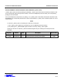
tests: carpeta con las pruebas implementadas. Contiene 6 pruebas:
• 8led.c: prueba en C para el visualizador de 8 segmentos.
• eight_led.adb: prueba en Ada para el visualizador de 8 segmentos.
• test_ic_rtc.adb: pone a prueba el funcionamiento del driver controlador de
interrupciones y el reloj de tiempo real. Cada vez que el contador del reloj se
desborda (cada segundo aproximadamente), avanza en 1 unidad el número
mostrado en el visualizador de 8 segmentos.
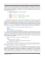
• test_ic_rtc_pwm.adb: pone a prueba el funcionamiento del driver controlador
de interrupciones, el reloj de tiempo real y el temporizador PWM. Para verificar
el correcto funcionamiento de las interrupciones, se instala un manejador básico
que actúa sobre el visualizador de 8 segmentos, poniéndolo a 1 y a 0 cada vez
que salta la interrupción (salta cada vez que el reloj se desborda). Asimismo,
cada 3 desbordamientos se desactiva la interrupción si estaba activada, o se
activa en caso contrario, verificando la correcta activación/desactivación. Puede
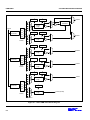
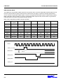
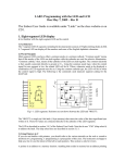
verse un esquema de la máquina de estados que representa la ejecución de este
programa en la figura A.1.
• test_ic_rtc_pwm_pr_1.adb, test_ic_rtc_pwm_pr_2.adb: idem que el anterior,
pero las interrupciones se deshabilitan con distintas llamadas a la interfaz
(deshabilitando todas las interrupciones a la vez o actuando sobre el registro de
estado). Puede verse un esquema de la máquina de estados que representa las
ejecuciones de estos programas en la figura A.1.
utils: carpeta que contiene los scripts de compilación automática.
Figura A.1. Diagrama de estados para las pruebas de habilitación/deshabilitación de
interrupciones.
Septiembre 2010
23
Migración del sistema operativo de tiempo real MaRTE OS al microprocesador ARM
La estructura que siguen los ficheros implementados puede verse en la figura A.2.
A.2. Estructura de los ficheros implementados.
A.1. Estructura de los proyectos.
Una vez ejecutamos el script “newProyect”, se genera una carpeta (cuyo nombre es el
primer parámetro de la invocación) con el siguiente contenido:
–
–
–
–
–
–
–
Examples: carpeta con fuentes para las pruebas.
Include, Lib: carpeta con bibliotecas necesarias para la compilación.
Link: carpeta con los ficheros para el linker.
Obj: carpeta con los ficheros objeto de la interfaz abstracta con el hardware.
Src: carpeta con programas C y Ada vacíos.
Startup: contiene los ficheros objeto de las rutinas de inicialización, reseteo y
definición del vector de interrupciones.
Diversos scripts:
+ compileTestC_ram: compila la prueba en C para el visualizador de 8 segmentos
para cargar en la RAM.
+ compileTestAda_ram: idem que el anterior pero para la prueba en Ada.
+ compileAda: acepta un parámetro, que debe ser el nombre del fichero de
cualquiera de las otras 4 pruebas implementadas eliminando la extensión. Se
generarán 2 ficheros como resultado de la compilación: “startup_flash” (para cargar
en la Flash, con la definición del vector de interrupciones y demás rutinas estáticas)
y otro que será el resultado de concatenar el parámetro introducido con “_ram”
(para cargar en la RAM, con el programa a ejecutar). El programa debe comenzar a
ejecutarse siempre desde la dirección 0, que coincide con la llamada a la rutina de
reseteo/inicialización. En el manual on-line de EmbestIDE [11] se muestra como
cargar en la placa de desarrollo un ejecutable.
Septiembre 2010
24
Migración del sistema operativo de tiempo real MaRTE OS al microprocesador ARM
Anexo B. Plan de Gestión del Proyecto
Software.
Este anexo es un resumen del Plan de Gestión del Proyecto Software empleado en el
desarrollo de este Proyecto Fin de Carrera.
B.1.- Elementos entregados.
Los elementos entregados como resultado de este Proyecto se clasifican en 2 grandes
grupos: la entrega escrita y la entrega en formato electrónico.
La entrega escrita la componen todos los documentos impresos en papel:
–
–
–
–
La propuesta del proyecto: contiene los objetivos que el proyectando se
compromete a completar, además de información personal. Este documento fue
entregado en cuanto el estado del proyecto permitió establecer un hito alcanzable.
El informe del director (en español e inglés): evalúa y comenta brevemente el
trabajo realizado por el proyectando.
La ficha de depósito (en español e ingles): incluye los elementos necesarios para
poder clasificar el proyecto en la biblioteca, además de un resumen de los objetivos
y las conclusiones del mismo.
La memoria final: recoge el trabajo realizado en este Proyecto Fin de Carrera. Se
seguirán las indicaciones de la guía de estilo.
La entrega en formato electrónico la componen los elementos entregados en el DVD
adjunto a la memoria. El formato de todos los ficheros con texto es .pdf (a excepción del
fichero README) y el de los comprimidos .rar. Los ficheros entregados son los siguientes:
–
–
–
–
–
–
–
La memoria final: idéntica a la escrita.
La máquina virtual: un fichero comprimido con una máquina virtual Ubuntu que
dispone del entorno de desarrollo cruzado ya instalado, así como todos los ficheros
necesarios para generarlo, una carpeta con los ficheros migrados y diversas
utilidades para probarlos. En el escritorio de dicha máquina hay un fichero README
que informa del contenido exacto. Para entrar en sesión usar como nombre de
usuario “luis” y contraseña “luisluis”.
Carpeta con fuentes para la instalación del entorno cruzado en Linux: idéntica a la
de la máquina virtual.
Carpeta con los fuentes migrados: idéntica a la de la máquina virtual.
Carpeta con programas adicionales que deben ser instalados.
Carpeta con el fichero de configuración para la aplicación Flash Programmer y un
proyecto de prueba para EmbestIDE. Los ejecutables obtenidos en Linux deben
copiarse a la subcarpeta “debug” y renombrarse con “embest.elf”.
Fichero README: información general.
Además, se realizará una exposición oral del trabajo realizado en el Proyecto Fin de
Carrera que tendrá una duración máxima de 30 minutos. Adicionalmente se procederá a la
carga de la memoria del proyecto en el repositorio ZAGUAN de la Universidad de Zaragoza.
Septiembre 2010
25
Migración del sistema operativo de tiempo real MaRTE OS al microprocesador ARM
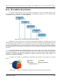
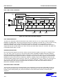
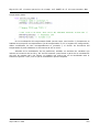
B.2.- El modelo de proceso.
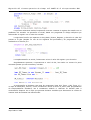
El ciclo de vida seguido en este proyecto se ajusta a un ciclo en cascada clásico [14]
(ver figura B.2.1). Este ciclo de vida aboga por la simplicidad y dado que es un proyecto de
corta duración (4-8 meses) es el más adecuado.
Figura B.2.1.- Ciclo de vida en cascada clásico.
Mediante el uso de este ciclo de vida ha sido posible identificar y reparar errores en la
misma fase en la que aparecen, con lo cual no se incurre en costes extra al identificar errores
en una determinada fase del ciclo de desarrollo y tener que realizar modificaciones sobre la
anterior. La documentación y revisión al final de cada una de las fases ha permitido identificar
con facilidad todos los problemas y riesgos que han ido surgiendo, facilitando el desarrollo del
proyecto.
En nuestro caso la fase de mantenimiento no existe, pero en un futuro es posible que
las sucesivas ampliaciones que deban llevarse a cabo en el código fuente requieran modificar
levemente elementos que han sido resultado de alguna de las otras fases. Estas ampliaciones
incluyen la migración completa de MaRTE OS a ARM (incluyendo soporte para tareas) o la
migración a otros procesadores.
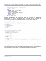
El tiempo (en horas) de dedicación a cada fase del proyecto viene dado en la figura
B.2.2.
42
12
128
Análisis
Diseño e
implementación
Pruebas
Documentación
82
Figura B.2.2. Tiempo de dedicación total de cada una de las fases del proyecto.
Septiembre 2010
26
Migración del sistema operativo de tiempo real MaRTE OS al microprocesador ARM
B.3.- Asunciones, dependencias y restricciones.
La estrategia de desarrollo de este producto Software se ha planeado de acuerdo a las
siguientes premisas:
–
–
–
–
–
Se dispone de una placa S3CEV40 sobre la que poder realizar las pruebas, en
perfecto estado y conectada correctamente a la corriente de alimentación. La
alimentación será suministrada con un conversor analógico-digital a 5v o con un
conector USB macho-hembra.
Para la carga de programas será necesario disponer de un conector USB adicional
macho-hembra o un cable Ethernet.
Será necesario además un emulador JTAG UNETICE, el cual deberá ser conectado a
la placa de desarrollo a través de un bus paralelo de 20 pines. A través de él se
realizará la carga de programas.
Se dispone de un PC con el sistema operativo Linux (Ubuntu) instalado,
convenientemente refrigerado y conectado a la corriente eléctrica. Al menos se
necesita 1 GB de memoria RAM.
La aplicación VirtualBox debe estar instalada en el PC.
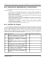
B.4.- Gestión de riesgos.
En la tabla B.4.1 se clasifican los diferentes tipos de riesgo encontrados a lo largo del
proyecto y que han amenazado el proceso de desarrollo del mismo. La columna “riesgo” indica
cual es la probabilidad estimada en porcentaje de que el riesgo de esa fila ocurra, mientras
que la columna “descripción” indica en detalle en que consiste dicho riesgo. La columna
“puntos” indica la gravedad del riesgo en caso de ocurrir, y la columna “estrategia de
mitigación” indica el método de la tabla B.4.2 seguido para intentar reducir la posibilidad de
que el riesgo se convierta en realidad y su gravedad.
Riesgo
Descripción
70
Proceso de configuración del entorno de 90
desarrollo cruzado en Linux no es trivial y
documentación en la Web inconsistente.
1
80
Dificultad
de
adaptación
al
entorno 30
proporcionado por el fabricante de la placa
de desarrollo.
2
5
El hardware utilizado no está en correcto 10
estado.
3
60
La arquitectura del sistema operativo 30
MaRTE OS no es trivial o fácil de entender.
2
100
Desconocimiento
de
los
periféricos 20
disponibles en el microcontrolador utilizado.
2
20
El
modelo
de
interrupciones
microcontrolador es muy complejo.
del 80
2
5
La falta de experiencia en los lenguajes de 15
programación C y Ada hacen retrasan el
desarrollo.
4
Septiembre 2010
Puntos
Estrategia de mitigación
27
Migración del sistema operativo de tiempo real MaRTE OS al microprocesador ARM
40
El equipo sobre el que se guardan los 100
ficheros del proyecto se rompe o deteriora.
5
La tabla B.4.2 muestra las estrategias de mitigación empleadas sobre los riesgos
enumerados en la tabla B.4.1.
Número de estrategia de mitigación
Descripción
1
Consulta con diferentes expertos en el tema,
con el fin de renovar las fuentes en uso.
2
Consulta de la documentación disponible en la
Web o los CD's del fabricante.
3
Cambio del hardware que el proyectando tiene
actualmente por otro igual.
4
Dedicación de más tiempo al desarrollo.
5
Mantener copias de seguridad del trabajo
realizado en un dispositivo USB.
B.5.- Herramientas.
Las herramientas Software empleadas en este Proyecto Fin de Carrera se enumeran a
continuación:
–
–
–
–
–
–
–
–
–
–
–
–
–
Sistema operativo: Windows XP.
Explorador Web: Internet Explorer.
Paquete de ofimática: OpenOffice v3.1.0.
Herramienta de dibujo: Paint v5.1.
Gestor/Emulador de máquinas virtuales: VirtualBox v3.1.4.
Sistema operativo (emulado): Ubuntu.
Utilidades binarias: Binutils 2.20.1.
Librerías de operaciones matemáticas: GMP 4.3.2 y MPFR 2.4.2.
Librería estándar de C: Newlib 1.18.0.
Fuentes del compilador C con sus extensiones Ada: GCC 4.4.4.
Entorno de desarrollo, carga y depuración de programas para la placa de desarrollo
S3CEV40: Embest IDE.
Aplicación de carga de aplicaciones en la memoria RAM de la placa de desarrollo
S3CEV40: Flash Programmer.
Aplicación auxiliar de análisis y mantenimiento de memoria dinámica: Valgrind v3.5.
B.6.- Paquetes de trabajo.
10000 Gestión del proyecto
11000 Reuniones con el tutor
12000 Presentación ante tribunal
12100 Borrador
12200 Ensayos
12300 Realización
20000 Desarrollo del proyecto
Septiembre 2010
28
Migración del sistema operativo de tiempo real MaRTE OS al microprocesador ARM
21000 Fase de análisis
21100 Sistema operativo MaRTE OS
21110 Estudio de la documentación Web
21120 Pruebas iniciales para comprender su funcionamiento
21200 Placa de desarrollo S3CEV40
21210 Estudio de la documentación del fabricante de la placa
21220 Pruebas iniciales para verificar su funcionamiento
21300 Entorno de desarrollo cruzado
21310 Estudio de la documentación Web
21320 Estudio de la documentación del fabricante de la placa
21400 Propuesta del PFC
21410 Especificación de objetivos
21420 Borrador de la propuesta
21430 Reunión con el tutor
21440 Propuesta definitiva
21500 Revisión del proceso de análisis
22000 Fase de diseño
22100 Entorno de desarrollo cruzado
22110 Entorno cruzado en Ubuntu
22111 Configuración del entorno
22122 Pruebas para verificación
22220 Entorno de carga/depuración en Windows
22221 Especificación de la carga de programas
22200 Placa de desarrollo S3CEV40
22210 Elección de los periféricos a utilizar
22220 Especificación de drivers
22211 Especificación del driver para el controlador de
interrupciones
22212 Especificación del driver para el reloj de tiempo
real
22213 Especificación del driver para el temporizador
PWM
22300 Sistema operativo MaRTE OS
22310 Especificación de la estrategia de implementación
22320 Definición de las operaciones de alto nivel
22330 Definición de alto nivel de las pruebas finales
22331 Pruebas generales sobre la placa
22332 Pruebas especificas sobre los drivers diseñados
22400 Revisión del diseño realizado
23000 Fase de implementación
23100 Interfaz abstracta con el hardware de MaRTE OS
23200 Drivers para periféricos
23210 Driver para el controlador de interrupciones
23220 Driver para el reloj de tiempo real
23230 Driver para el temporizador PWM
23300 Módulos auxiliares
23310 Operaciones con a nivel de bit
23320 Operaciones con tiempos
23400 Ficheros de arranque del microcontrolador
23500 Revisión de la implementación
Septiembre 2010
29
Migración del sistema operativo de tiempo real MaRTE OS al microprocesador ARM
24000 Fase de pruebas
24100 Implementación de las pruebas definidas
24200 Script's auxiliares
24210 Compilación automática de los fuentes
24220 Compilación automática de las pruebas
24230 Generación de carpetas de trabajo independientes
24300 Verificación y validación de los resultados de las pruebas
24400 Revisión de las pruebas realizadas
25000 Gestión de la configuración
25100 Gestión de la documentación
25110 Copias de seguridad semanales a USB
25200 Gestión del código
25210 Copias de seguridad semanales a USB
25220 Control de versiones manual
25300 Impresión de los elementos a entregar
25400 Preparación de la carpeta con los elementos a enviar
26000 Documentación
26100 Memoria del proyecto
26200 Anexos
26210 Estructura de los ficheros migrados
26220 Plan de Gestión del Proyecto Software
26230 Instalación de MaRTE OS y compilación de aplicaciones
26240 Resumen del repertorio de instrucciones del ARM7tdmi
26250 Registros principales y excepciones del ARM7tdmi
26260 Documentación especifica de los periféricos utilizados
26270 Aspectos de bajo nivel de la implementación
26280 Configuración del compilador cruzado en Linux y carga
de aplicaciones desde Windows
Septiembre 2010
30
Migración del sistema operativo de tiempo real MaRTE OS al microprocesador ARM
Anexo C. Instalación de MaRTE OS y
compilación de aplicaciones.
Este anexo contiene un extracto traducido y modificado del manual de instalación
original de MaRTE OS, alojado en la página de la Universidad de Cantabria.
Los requerimientos de instalación de MaRTE OS son los siguientes:
–
Requerimientos del Host (requerido para las 2 implementaciones de MaRTE OS para
Linux, la de X86 y la de ARM):
•
•
•
–
Requerimientos del Target en caso de implementación para x86:
•
•
•
–
Sistema operativo Linux.
Compilador GNAT (nativo o cruzado según el caso).
Sistema operativo Windows con EmbestIDE para realizar la carga de los
ejecutables generados en Linux (solo para ARM).
PC i386 o superior.
Tarjeta Ethernet para carga remota (opcional).
Puerto serie para depuración (opcional).
Requerimientos del Target en caso de implementación para ARM:
•
•
•
•
•
•
Microcontrolador S3C44B0X o cualquiera compatible.
Placa de desarrollo S3CEV40 (opcional para las pruebas).
Toma de corriente alterna para alimentación de la placa S3CEV40.
Puerto USB para alimentación y carga de aplicaciones por el JTAG.
Toma de corriente alterna para alimentación alternativa del JTAG (opcional).
Puerto USB para alimentación alternativa de la placa S3CEV40 (opcional).
Paso 0: Instalación del compilador GNAT.
MaRTE OS está escrito en Ada. Pese a que el programador no quiera compilar
aplicaciones Ada bajo este sistema operativo (por ejemplo, aplicaciones escritas en C o C++),
será necesario obtener el compilador GNAT correspondiente para poder compilar el núcleo de
MaRTE OS.
En nuestro caso, la instalación del compilador no es un proceso trivial, por lo que ha
sido necesario incluir un anexo diferente del actual (el anexo J, con los pasos necesarios para
configurar el compilador cruzado en Linux). Para el caso de las implementaciones de MaRTE OS
previas la instalación de GNAT es muy sencilla, pudiéndose realizar en el propio directorio de
trabajo sin afectar al resto del sistema. Hay que tener en cuenta que cada versión de MaRTE
OS soporta un subconjunto de versiones del compilador, por lo que el programador deberá
asegurarse de utilizar la versión correcta.
Para instalar el compilador GNAT habrá que descargarlo de la página de Libre Adacore.
Septiembre 2010
31
Migración del sistema operativo de tiempo real MaRTE OS al microprocesador ARM
Tras descomprimir los ficheros y ejecutar un script el compilador estará listo para ser utilizado.
Los pasos a realizar en línea de comandos son los siguientes:
$
$
$
$
cd $HOME/myapps
tar -zxvf gnat-gpl-2008-i686-gnu-linux-gnu-libc2.3-bin.tar.gz
cd gnat-gpl-2008-i686-gnu-linux-gnu-libc2.3-bin
./doinstall
Para que la instalación no afecte al resto del sistema, escoger un directorio de
instalación distinto al directorio por defecto (por ejemplo $HOME/myapps). Después de la
instalación habrá que incluir los binarios GNAT delante del PATH con el siguiente comando:
$ export PATH=$HOME/myapps/gnat/bin:$PATH
Para no tener que ejecutar este comando cada vez que se entre al sistema, es
recomendable incluirlo en el script de inicio del shell ($HOME/.bashrc).
Paso 1: Instalación de MaRTE OS.
En el caso de la arquitectura de MaRTE OS objetivo del actual PFC el sistema no está
totalmente listo para ser compilado: faltan determinadas funcionalidades por migrar. Sin
embargo, para las arquitecturas previas (y en un futuro para nuestra arquitectura objetivo) el
sistema operativo es muy facil de instalar.
Para instalar el sistema bastará con descargar y descomprimir los ficheros de MaRTE OS
(descargables desde la página de la Universidad de Cantabria) y ejecutar un script de
instalación. Deberán usarse los siguientes comandos:
$
$
$
$
cd $HOME
tar -zxvf marte-version.tar.gz
cd marte
./minstall
El funcionamiento de minstall es muy sencillo. Únicamente buscará la instalación de
GNAT (realizada en el paso 0) y realizará algunos enlaces simbólicos desde el directorio de
descompresión de MaRTE OS. Tras la instalación es recomendable incluir el directorio utils del
directorio de MaRTE OS, con el fin de emplear sus utilidades con mayor comodidad. Usar el
siguiente comando:
$ export PATH=$PATH:$HOME/marte/utils
Es recomendable incluir el comando anterior en el script de inicio del sistema
($HOME/.bashrc).
En caso de estar empleando la versión binaria de MaRTE OS (con el núcleo previamente
compilado) el proceso de instalación habría sido completado. Con la versión de MaRTE actual,
pueden encontrarse dentro del directorio de descarga/instalación las librerías para las 3
plataformas soportadas: x86, Linux (lanzamiento de MaRTE OS como proceso de Linux) y
Linux_Lib (lanzamiento como proceso de Linux pero con acceso al sistema de ficheros y
drivers del sistema operativo). Cuando la versión para ARM esté completa, esta plataforma
aparecerá también entre las librerías.
En el caso de no estar empleando la versión binaria de MaRTE OS, será necesario
Septiembre 2010
32
Migración del sistema operativo de tiempo real MaRTE OS al microprocesador ARM
compilar su kernel y previamente el runtime de GNAT. Los siguientes comandos realizan la
compilación del runtime de GNAT para cada una de las versiones previas de MaRTE OS:
$ mkrtsmarteuc -march linux
$ mkrtsmarteuc -march linux_lib
$ mkrtsmarteuc -march x86 -mproc [i386 | pi | pii]
Una vez compilado el runtime de GNAT, deberá ejecutarse uno de los siguientes
comandos (dependiendo de la plataforma de ejecución de MaRTE OS escogida), con el fin de
compilar el kernel:
$ mkmarte -march linux
$ mkmarte -march linux_lib
$ mkmarte -march x86 -mproc [i386 | pi | pii]
Paso 2: Compilación de aplicaciones con MaRTE OS.
Antes de pasar al proceso de compilación será necesario establecer la arquitectura
destino para los ejecutables que se generarán. Los siguientes comandos establecen las
librerías (dependientes de la plataforma) a utilizar en el proceso de compilación de aplicaciones
con MaRTE OS:
$ msetcurrentarch -march linux
$ msetcurrentarch -march linux_lib
$ msetcurrentarch -march x86 -mproc [i386 | pi | pii]
A partir de este punto, podrán compilarse aplicaciones en C, C++ y Ada de la misma
forma que podían compilarse aplicaciones nativas con compiladores tradicionales. En el
subdirectorio examples del directorio principal de marte hay diversos ejemplos que pueden
usarse para comprobar la correcta instalación del sistema operativo. Los siguientes comandos
(con nombre prácticamente igual a los tradicionalmente utilizados) invocarán los scripts de
MaRTE OS (ya incluídos en el PATH) y realizarán la compilación del ejemplo "hola mundo" con
los 3 lenguajes soportados:
$ mgcc hello_world_c.c (for a C application)
$ mgnatmake hello_world.adb (for an Ada application)
$ mg++ hello_world_cpp.cc (for a C++ application)
Las opciones que admite cada uno de los scripts son las mismas que admitirían los
comandos originales de compilación. Para continuar con el proceso de carga de programas
compilados en el microcontrolador utilizado (de cara a cuando MaRTE OS este completamente
migrado a la nueva arquitectura) puede consultarse el manual on-line de EmbestIDE [11].
En el caso de estar compilando para Linux (versión Linux o Linux_Lib) bastaría con
ejecutar el programa compilado para verificar su funcionamiento. En el caso de la versión para
X86 sería necesario incluir el programa compilado entre las opciones de arranque (con
aplicaciones como WinGrub [15], que permite configurar dicho arranque desde Windows), y
arrancar directamente con él.
Septiembre 2010
33
Migración del sistema operativo de tiempo real MaRTE OS al microprocesador ARM
Anexo D. Resumen del repertorio de
instrucciones del ARM7tdmi.
Este anexo es un extracto del capítulo 3 (INSTRUCTION SET) del manual original del
microcontrolador.
Septiembre 2010
34
S3C44B0X RISC MICROPROCESSOR
ARM INSTRUCTION SET
INSTRUCTION SET SUMMARY
This chapter describes the ARM instruction set in the ARM7TDMI core.
FORMAT SUMMARY
The ARM instruction set formats are shown below.
31 30 29 28 27 26 25 24 23 22 21 20 19 18 17 16 15 14 13 12 11 10 9 8 7 6 5 4 3 2 1 0
Cond
0 0 I
Opcode S
Rn
Rd
Cond
0 0 0 0 0 0 A S
Rd
Rn
Rs
1 0 0 1
Rm
Multiply
Cond
0 0 0 0 1 U A S
RdHi
RdLo
Rn
1 0 0 1
Rm
Multiply Long
Cond
0 0 0 1 0 B 0 0
Rn
Rd
0 0 0 0 1 0 0 1
Rm
Single Data Swap
Cond
0 0 0 1 0 0 1 0 1 1 1 1 1 1 1 1 1 1 1 1 0 0 0 1
Rn
Branch and Exchange
Cond
0 0 0 P U 0 W L
Rn
Rd
Rm
Halfword Data Transfer:
register offset
Cond
0 0 0 P U 1 W L
Rn
Rd
Offset
Halfword Data Transfer:
immendiate offset
Cond
0 1 I P U BW L
Rn
Rd
Cond
0 1 I
Cond
1 0 0 P U BW L
Cond
1 0 1 L
Cond
1 1 0 P U BW L
Cond
1 1 1 0
Cond
1 1 1 0
Cond
1 1 1 1
Data/Processing/
PSR Transfer
Operand2
0 0 0 0 1 S H 1
Offset
1 S H 1
Offset
Single Data Transfer
1
Rn
Undefined
Register List
Block Data Transfer
Offset
Branch
Rn
CRd
CP#
CP Opc
CRn
CRd
CP#
CP
0
CRm
Coprocessor Data Operation
CP
Opc
CRn
Rd
CP#
CP
1
CRm
Coprocessor Register Transfer
L
Offset
Coprocessor Data Transfer
Ignored by processor
Software Interrupt
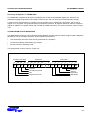
31 30 29 28 27 26 25 24 23 22 21 20 19 18 17 16 15 14 13 12 11 10 9 8 7 6 5 4 3 2 1 0
Figure 3-1. ARM Instruction Set Format
NOTE
Some instruction codes are not defined but do not cause the Undefined instruction trap to be taken, for
instance a Multiply instruction with bit 6 changed to a 1. These instructions should not be used, as their
action may change in future ARM implementations.
3-1
ARM INSTRUCTION SET
S3C44B0X RISC MICROPROCESSOR
INSTRUCTION SUMMARY
Table 3-1. The ARM Instruction Set
Mnemonic
Instruction
Action
ADC
Add with carry
Rd: = Rn + Op2 + Carry
ADD
Add
Rd: = Rn + Op2
AND
AND
Rd: = Rn AND Op2
B
Branch
R15: = address
BIC
Bit Clear
Rd: = Rn AND NOT Op2
BL
Branch with Link
R14: = R15, R15: = address
BX
Branch and Exchange
R15: = Rn, T bit: = Rn[0]
CDP
Coprocessor Data Processing
(Coprocessor-specific)
CMN
Compare Negative
CPSR flags: = Rn + Op2
CMP
Compare
CPSR flags: = Rn - Op2
EOR
Exclusive OR
Rd: = (Rn AND NOT Op2)
OR (Op2 AND NOT Rn)
LDC
Load coprocessor from memory
Coprocessor load
LDM
Load multiple registers
Stack manipulation (Pop)
LDR
Load register from memory
Rd: = (address)
MCR
Move CPU register to coprocessor
register
cRn: = rRn {<op>cRm}
MLA
Multiply Accumulate
Rd: = (Rm × Rs) + Rn
MOV
Move register or constant
Rd: = Op2
3-2
S3C44B0X RISC MICROPROCESSOR
ARM INSTRUCTION SET
Table 3-1. The ARM Instruction Set (Continued)
Mnemonic
Instruction
Action
MRC
Move from coprocessor register to
CPU register
Rn: = cRn {<op>cRm}
MRS
Move PSR status/flags to register
Rn: = PSR
MSR
Move register to PSR status/flags
PSR: = Rm
MUL
Multiply
Rd: = Rm × Rs
MVN
Move negative register
Rd: = 0 × FFFFFFFF EOR Op2
ORR
OR
Rd: = Rn OR Op2
RSB
Reverse Subtract
Rd: = Op2 - Rn
RSC
Reverse Subtract with Carry
Rd: = Op2 - Rn - 1 + Carry
SBC
Subtract with Carry
Rd: = Rn - Op2 - 1 + Carry
STC
Store coprocessor register to memory
address: = CRn
STM
Store Multiple
Stack manipulation (Push)
STR
Store register to memory
<address>: = Rd
SUB
Subtract
Rd: = Rn - Op2
SWI
Software Interrupt
OS call
SWP
Swap register with memory
Rd: = [Rn], [Rn] := Rm
TEQ
Test bitwise equality
CPSR flags: = Rn EOR Op2
TST
Test bits
CPSR flags: = Rn AND Op2
3-3
ARM INSTRUCTION SET
S3C44B0X RISC MICROPROCESSOR
THE CONDITION FIELD
In ARM state, all instructions are conditionally executed according to the state of the CPSR condition codes and
the instruction's condition field. This field (bits 31:28) determines the circumstances under which an instruction is
to be executed. If the state of the C, N, Z and V flags fulfils the conditions encoded by the field, the instruction is
executed, otherwise it is ignored.
There are sixteen possible conditions, each represented by a two-character suffix that can be appended to the
instruction's mnemonic. For example, a Branch (B in assembly language) becomes BEQ for "Branch if Equal",
which means the Branch will only be taken if the Z flag is set.
In practice, fifteen different conditions may be used: these are listed in Table 3-2. The sixteenth (1111) is
reserved, and must not be used.
In the absence of a suffix, the condition field of most instructions is set to "Always" (suffix AL). This means the
instruction will always be executed regardless of the CPSR condition codes.
Table 3-2. Condition Code Summary
3-4
Code
Suffix
Flags
Meaning
0000
EQ
Z set
equal
0001
NE
Z clear
not equal
0010
CS
C set
unsigned higher or same
0011
CC
C clear
unsigned lower
0100
MI
N set
negative
0101
PL
N clear
positive or zero
0110
VS
V set
overflow
0111
VC
V clear
no overflow
1000
HI
C set and Z clear
unsigned higher
1001
LS
C clear or Z set
unsigned lower or same
1010
GE
N equals V
greater or equal
1011
LT
N not equal to V
less than
1100
GT
Z clear AND (N equals V)
greater than
1101
LE
Z set OR (N not equal to V)
less than or equal
1110
AL
(ignored)
always
Migración del sistema operativo de tiempo real MaRTE OS al microprocesador ARM
Anexo E. Registros principales y excepciones
del ARM7tdmi.
Este anexo es un extracto del manual original del microcontrolador y corresponde al
capítulo 4 (PROGRAMMER'S MODEL) del mismo.
Septiembre 2010
39
S3C44B0X RISC MICROPROCESSOR
PROGRAMMER'S MODEL
OVERVIEW
S3C44B0X has been developed using the advanced ARM7TDMI core, which has been designed by Advanced
RISC Machines, Ltd.
PROCESSOR OPERATING STATES
From the programmer's point of view, the ARM7TDMI can be in one of two states:
•
ARM state which executes 32-bit, word-aligned ARM instructions.
•
THUMB state which can execute 16-bit, halfword-aligned THUMB instructions. In this state, the PC uses bit 1
to select between alternate halfwords.
NOTE
Transition between these two states does not affect the processor mode or the contents of the registers.
SWITCHING STATE
Entering THUMB State
Entry into THUMB state can be achieved by executing a BX instruction with the state bit (bit 0) set in the operand
register.
Transition to THUMB state will also occur automatically on return from an exception (IRQ, FIQ, UNDEF, ABORT,
SWI etc.), if the exception was entered with the processor in THUMB state.
Entering ARM State
Entry into ARM state happens:
•
On execution of the BX instruction with the state bit clear in the operand register.
•
On the processor taking an exception (IRQ, FIQ, RESET, UNDEF, ABORT, SWI etc.). In this case, the PC is
placed in the exception mode's link register, and execution commences at the exception's vector address.
MEMORY FORMATS
ARM7TDMI views memory as a linear collection of bytes numbered upwards from zero. Bytes 0 to 3 hold the first
stored word, bytes 4 to 7 the second and so on. ARM7TDMI can treat words in memory as being stored either in
Big-Endian or Little-Endian format.
2-1
PROGRAMMER'S MODEL
S3C44B0X RISC MICROPROCESSOR
BIG-ENDIAN FORMAT
In Big-Endian format, the most significant byte of a word is stored at the lowest numbered byte and the least
significant byte at the highest numbered byte. Byte 0 of the memory system is therefore connected to data lines
31 through 24.
Higher Address
Word Address
31
Lower Address
24
23
16
15
8
7
0
8
9
10
11
8
4
5
6
7
4
0
1
2
3
0
Most significant byte is at lowest address.
Word is addressed by byte address of most significant byte.
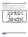
Figure 2-1. Big-Endian Addresses of Bytes within Words
LITTLE-ENDIAN FORMAT
In Little-Endian format, the lowest numbered byte in a word is considered the word's least significant byte, and
the highest numbered byte the most significant. Byte 0 of the memory system is therefore connected to data lines
7 through 0.
Higher Address
Word Address
31
Lower Address
24
23
16
15
8
7
0
11
10
9
8
8
7
6
5
4
4
3
2
1
0
0
Least significant byte is at lowest address.
Word is addressed by byte address of least significant byte.
Figure 2-2. Little-Endian Addresses of Bytes whthin Words
INSTRUCTION LENGTH
Instructions are either 32 bits long (in ARM state) or 16 bits long (in THUMB state).
Data Types
ARM7TDMI supports byte (8-bit), halfword (16-bit) and word (32-bit) data types. Words must be aligned to fourbyte boundaries and half words to two-byte boundaries.
2-2
S3C44B0X RISC MICROPROCESSOR
PROGRAMMER'S MODEL
OPERATING MODES
ARM7TDMI supports seven modes of operation:
•
User (usr): The normal ARM program execution state
•
FIQ (fiq): Designed to support a data transfer or channel process
•
IRQ (irq): Used for general-purpose interrupt handling
•
Supervisor (svc): Protected mode for the operating system
•
Abort mode (abt): Entered after a data or instruction prefetch abort
•
System (sys): A privileged user mode for the operating system
•
Undefined (und): Entered when an undefined instruction is executed
Mode changes may be made under software control, or may be brought about by external interrupts or exception
processing. Most application programs will execute in User mode. The non-user modes' known as privileged
modes-are entered in order to service interrupts or exceptions, or to access protected resources.
REGISTERS
ARM7TDMI has a total of 37 registers - 31 general-purpose 32-bit registers and six status registers - but these
cannot all be seen at once. The processor state and operating mode dictate which registers are available to the
programmer.
The ARM State Register Set
In ARM state, 16 general registers and one or two status registers are visible at any one time. In privileged (nonUser) modes, mode-specific banked registers are switched in. Figure 2-3 shows which registers are available in
each mode: the banked registers are marked with a shaded triangle.
The ARM state register set contains 16 directly accessible registers: R0 to R15. All of these except R15 are
general-purpose, and may be used to hold either data or address values. In addition to these, there is a
seventeenth register used to store status information.
Register 14
is used as the subroutine link register. This receives a copy of R15 when a Branch
and Link (BL) instruction is executed. At all other times it may be treated as a
general-purpose register. The corresponding banked registers R14_svc, R14_irq,
R14_fiq, R14_abt and R14_und are similarly used to hold the return values of R15
when interrupts and exceptions arise, or when Branch and Link instructions are
executed within interrupt or exception routines.
Register 15
holds the Program Counter (PC). In ARM state, bits [1:0] of R15 are zero and bits
[31:2] contain the PC. In THUMB state, bit [0] is zero and bits [31:1] contain the PC.
Register 16
is the CPSR (Current Program Status Register). This contains condition code flags
and the current mode bits.
FIQ mode has seven banked registers mapped to R8-14 (R8_fiq-R14_fiq). In ARM state, many FIQ handlers do
not need to save any registers. User, IRQ, Supervisor, Abort and Undefined each have two banked registers
mapped to R13 and R14, allowing each of these modes to have a private stack pointer and link registers.
2-3
PROGRAMMER'S MODEL
S3C44B0X RISC MICROPROCESSOR
ARM State General Registers and Program Counter
System & User
R0
R1
R2
R3
R4
R5
R6
R7
R8
R9
R10
R11
R12
R13
R14
R15 (PC)
FIQ
R0
R1
R2
R3
R4
R5
R6
R7
R8_fiq
R9_fiq
R10_fiq
R11_fiq
R12_fiq
R13_fiq
R14_fiq
R15 (PC)
Supervisor
R0
R1
R2
R3
R4
R5
R6
R7
R8
R9
R10
R11
R12
R13_svc
R14_svc
R15 (PC)
Abort
R0
R1
R2
R3
R4
R5
R6
R7
R8
R9
R10
R11
R12
R13_abt
R14_abt
R15 (PC)
IRQ
R0
R1
R2
R3
R4
R5
R6
R7
R8
R9
R10
R11
R12
R13_irq
R14_irq
R15 (PC)
Undefined
R0
R1
R2
R3
R4
R5
R6
R7
R8
R9
R10
R11
R12
R13_und
R14_und
R15 (PC)
ARM State Program Status Registers
CPSR
CPSR
SPSR_fiq
CPSR
SPSR_svc
CPSR
CPSR
SPSR_abt
SPSR_irq
= banked register
Figure 2-3. Register Organization in ARM State
2-4
CPSR
SPSR_und
S3C44B0X RISC MICROPROCESSOR
PROGRAMMER'S MODEL
The THUMB State Register Set
The THUMB state register set is a subset of the ARM state set. The programmer has direct access to eight
general registers, R0-R7, as well as the Program Counter (PC), a stack pointer register (SP), a link register (LR),
and the CPSR. There are banked Stack Pointers, Link Registers and Saved Process Status Registers (SPSRs)
for each privileged mode. This is shown in Figure 2-4.
THUMB State General Registers and Program Counter
System & User
R0
R1
R2
R3
R4
R5
R6
R7
SP
LR
PC
FIQ
Supervisor
Abort
IRQ
Undefined
R0
R1
R2
R3
R4
R5
R6
R7
SP_fiq
LR_fiq
PC
R0
R1
R2
R3
R4
R5
R6
R7
SP_svc
LR_svc
PC
R0
R1
R2
R3
R4
R5
R6
R7
SP_abt
LR_abt
PC
R0
R1
R2
R3
R4
R5
R6
R7
SP_und
LR_und
PC
R0
R1
R2
R3
R4
R5
R6
R7
SP_fiq
LR_fiq
PC
THUMB State Program Status Registers
CPSR
CPSR
SPSR_fiq
CPSR
SPSR_svc
CPSR
CPSR
SPSR_abt
SPSR_irq
CPSR
SPSR_und
= banked register
Figure 2-4. Register Organization in THUMB State
2-5
PROGRAMMER'S MODEL
S3C44B0X RISC MICROPROCESSOR
The relationship between ARM and THUMB state registers
The THUMB state registers relate to the ARM state registers in the following way:
•
THUMB state R0-R7 and ARM state R0-R7 are identical
•
THUMB state CPSR and SPSRs and ARM state CPSR and SPSRs are identical
•
THUMB state SP maps onto ARM state R13
•
THUMB state LR maps onto ARM state R14
•
The THUMB state Program Counter maps onto the ARM state Program Counter (R15)
ARM state
R0
R1
R2
R3
R4
R5
R6
R7
Stack Pointer (SP)
Link register (LR)
R0
R1
R2
R3
R4
R5
R6
R7
R8
R9
R10
R11
R12
Stack Pointer (R13)
Link register (R14)
Program Counter (PC)
CPSR
SPSR
Program Counter (R15)
CPSR
SPSR
Hi-registers
THUMB state
Lo-registers
This relationship is shown in Figure 2-5.
Figure 2-5. Mapping of THUMB State Registers onto ARM State Registers
2-6
S3C44B0X RISC MICROPROCESSOR
PROGRAMMER'S MODEL
Accessing Hi-Registers in THUMB State
In THUMB state, registers R8-R15 (the Hi registers) are not part of the standard register set. However, the
assembly language programmer has limited access to them, and can use them for fast temporary storage.
A value may be transferred from a register in the range R0-R7 (a Lo register) to a Hi register, and from a Hi
register to a Lo register, using special variants of the MOV instruction. Hi register values can also be compared
against or added to Lo register values with the CMP and ADD instructions. For more information, refer to Figure
3-34.
THE PROGRAM STATUS REGISTERS
The ARM7TDMI contains a Current Program Status Register (CPSR), plus five Saved Program Status Registers
(SPSRs) for use by exception handlers. These register's functions are:
•
Hold information about the most recently performed ALU operation
•
Control the enabling and disabling of interrupts
•
Set the processor operating mode
The arrangement of bits is shown in Figure 2-6.
Condition Code Flags
30
29
28
N
Z
C
V
27
26
25
24
Control Bits
23
8
7
6
5
4
3
2
1
0
I
F
T
M4
M3
M2
M1
M0
~
~
31
(Reserved)
~
~
Overflow
Carry/Borrow/Extend
Zero
Negative/Less Than
Mode bits
State bit
FIQ disable
IRQ disable
Figure 2-6. Program Status Register Format
2-7
PROGRAMMER'S MODEL
S3C44B0X RISC MICROPROCESSOR
The Condition Code Flags
The N, Z, C and V bits are the condition code flags. These may be changed as a result of arithmetic and logical
operations, and may be tested to determine whether an instruction should be executed.
In ARM state, all instructions may be executed conditionally: see Table 3-2 for details.
In THUMB state, only the Branch instruction is capable of conditional execution: see Figure 3-46 for details.
The Control Bits
The bottom 8 bits of a PSR (incorporating I, F, T and M[4:0]) are known collectively as the control bits. These will
be changed when an exception arises. If the processor is operating in a privileged mode, they can also be
manipulated by software.
The T bit
This reflects the operating state. When this bit is set, the processor is executing in THUMB
state, otherwise it is executing in ARM state. This is reflected on the TBIT external signal.
Note that the software must never change the state of the TBIT in the CPSR. If this
happens, the processor will enter an unpredictable state.
Interrupt disable bits
The I and F bits are the interrupt disable bits. When set, these disable the IRQ and FIQ
interrupts respectively.
The mode bits
The M4, M3, M2, M1 and M0 bits (M[4:0]) are the mode bits. These determine the
processor's operating mode, as shown in Table 2-1. Not all combinations of the mode bits
define a valid processor mode. Only those explicitly described shall be used. The user
should be aware that if any illegal value is programmed into the mode bits, M[4:0], then the
processor will enter an unrecoverable state. If this occurs, reset should be applied.
Reserved bits
The remaining bits in the PSRs are reserved. When changing a PSR's flag or control bits,
you must ensure that these unused bits are not altered. Also, your program should not rely
on them containing specific values, since in future processors they may read as one or
zero.
2-8
S3C44B0X RISC MICROPROCESSOR
PROGRAMMER'S MODEL
Table 2-1. PSR Mode Bit Values
M[4:0]
Mode
Visible THUMB state registers
Visible ARM state registers
10000
User
R7..R0,
LR, SP
PC, CPSR
R14..R0,
PC, CPSR
10001
FIQ
R7..R0,
LR_fiq, SP_fiq
PC, CPSR, SPSR_fiq
R7..R0,
R14_fiq..R8_fiq,
PC, CPSR, SPSR_fiq
10010
IRQ
R7..R0,
LR_irq, SP_irq
PC, CPSR, SPSR_irq
R12..R0,
R14_irq, R13_irq,
PC, CPSR, SPSR_irq
10011
Supervisor
R7..R0,
LR_svc, SP_svc,
PC, CPSR, SPSR_svc
R12..R0,
R14_svc, R13_svc,
PC, CPSR, SPSR_svc
10111
Abort
R7..R0,
LR_abt, SP_abt,
PC, CPSR, SPSR_abt
R12..R0,
R14_abt, R13_abt,
PC, CPSR, SPSR_abt
11011
Undefined
R7..R0
LR_und, SP_und,
PC, CPSR, SPSR_und
R12..R0,
R14_und, R13_und,
PC, CPSR
11111
System
R7..R0,
LR, SP
PC, CPSR
R14..R0,
PC, CPSR
Reserved bits
The remaining bits in the PSR's are reserved. When changing a PSR's flag or control bits,
you must ensure that these unused bits are not altered. Also, your program should not rely
on them containing specific values, since in future processors they may read as one or
zero.
2-9
PROGRAMMER'S MODEL
S3C44B0X RISC MICROPROCESSOR
EXCEPTIONS
Exceptions arise whenever the normal flow of a program has to be halted temporarily, for example to service an
interrupt from a peripheral. Before an exception can be handled, the current processor state must be preserved
so that the original program can resume when the handler routine has finished.
It is possible for several exceptions to arise at the same time. If this happens, they are dealt with in a fixed order.
See Exception Priorities on page 2-14.
Action on Entering an Exception
When handling an exception, the ARM7TDMI:
1. Preserves the address of the next instruction in the appropriate Link Register. If the exception has been
entered from ARM state, then the address of the next instruction is copied into the Link Register (that is,
current PC + 4 or PC + 8 depending on the exception. See Table 2-2 on for details). If the exception has
been entered from THUMB state, then the value written into the Link Register is the current PC offset by a
value such that the program resumes from the correct place on return from the exception. This means that
the exception handler need not determine which state the exception was entered from. For example, in the
case of SWI, MOVS PC, R14_svc will always return to the next instruction regardless of whether the SWI
was executed in ARM or THUMB state.
2. Copies the CPSR into the appropriate SPSR
3. Forces the CPSR mode bits to a value which depends on the exception
4. Forces the PC to fetch the next instruction from the relevant exception vector
It may also set the interrupt disable flags to prevent otherwise unmanageable nestings of exceptions.
If the processor is in THUMB state when an exception occurs, it will automatically switch into ARM state when the
PC is loaded with the exception vector address.
Action on Leaving an Exception
On completion, the exception handler:
1. Moves the Link Register, minus an offset where appropriate, to the PC. (The offset will vary depending on the
type of exception.)
2. Copies the SPSR back to the CPSR
3. Clears the interrupt disable flags, if they were set on entry
NOTE
An explicit switch back to THUMB state is never needed, since restoring the CPSR from the SPSR
automatically sets the T bit to the value it held immediately prior to the exception.
2-10
S3C44B0X RISC MICROPROCESSOR
PROGRAMMER'S MODEL
Exception Entry/Exit Summary
Table 2-2 summarises the PC value preserved in the relevant R14 on exception entry, and the recommended
instruction for exiting the exception handler.
Table 2-2. Exception Entry/Exit
Return Instruction
Previous State
Notes
ARM R14_x
THUMB R14_x
BL
MOV PC, R14
PC + 4
PC + 2
1
SWI
MOVS PC, R14_svc
PC + 4
PC + 2
1
UDEF
MOVS PC, R14_und
PC + 4
PC + 2
1
FIQ
SUBS PC, R14_fiq, #4
PC + 4
PC + 4
2
IRQ
SUBS PC, R14_irq, #4
PC + 4
PC + 4
2
PABT
SUBS PC, R14_abt, #4
PC + 4
PC + 4
1
DABT
SUBS PC, R14_abt, #8
PC + 8
PC + 8
3
RESET
NA
–
–
4
NOTES:
1. Where PC is the address of the BL/SWI/Undefined Instruction fetch which had the prefetch abort.
2. Where PC is the address of the instruction which did not get executed since the FIQ or IRQ took priority.
3. Where PC is the address of the Load or Store instruction which generated the data abort.
4. The value saved in R14_svc upon reset is unpredictable.
FIQ
The FIQ (Fast Interrupt Request) exception is designed to support a data transfer or channel process, and in
ARM state has sufficient private registers to remove the need for register saving (thus minimising the overhead
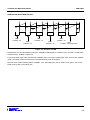
of context switching).
FIQ is externally generated by taking the nFIQ input LOW. This input can except either synchronous or
asynchronous transitions, depending on the state of the ISYNC input signal. When ISYNC is LOW, nFIQ and
nIRQ are considered asynchronous, and a cycle delay for synchronization is incurred before the interrupt can
affect the processor flow.
Irrespective of whether the exception was entered from ARM or Thumb state, a FIQ handler should leave the
interrupt by executing
SUBS
PC,R14_fiq,#4
FIQ may be disabled by setting the CPSR's F flag (but note that this is not possible from User mode). If the F flag
is clear, ARM7TDMI checks for a LOW level on the output of the FIQ synchroniser at the end of each instruction.
2-11
PROGRAMMER'S MODEL
S3C44B0X RISC MICROPROCESSOR
IRQ
The IRQ (Interrupt Request) exception is a normal interrupt caused by a LOW level on the nIRQ input. IRQ has a
lower priority than FIQ and is masked out when a FIQ sequence is entered. It may be disabled at any time by
setting the I bit in the CPSR, though this can only be done from a privileged (non-User) mode.
Irrespective of whether the exception was entered from ARM or Thumb state, an IRQ handler should return from
the interrupt by executing
SUBS
PC,R14_irq,#4
Abort
An abort indicates that the current memory access cannot be completed. It can be signalled by the external
ABORT input. ARM7TDMI checks for the abort exception during memory access cycles.
There are two types of abort:
•
Prefetch abort: occurs during an instruction prefetch.
•
Data abort: occurs during a data access.
If a prefetch abort occurs, the prefetched instruction is marked as invalid, but the exception will not be taken until
the instruction reaches the head of the pipeline. If the instruction is not executed - for example because a branch
occurs while it is in the pipeline - the abort does not take place.
If a data abort occurs, the action taken depends on the instruction type:
•
Single data transfer instructions (LDR, STR) write back modified base registers: the Abort handler must be
aware of this.
•
The swap instruction (SWP) is aborted as though it had not been executed.
•
Block data transfer instructions (LDM, STM) complete. If write-back is set, the base is updated. If the
instruction would have overwritten the base with data (ie it has the base in the transfer list), the overwriting is
prevented. All register overwriting is prevented after an abort is indicated, which means in particular that R15
(always the last register to be transferred) is preserved in an aborted LDM instruction.
The abort mechanism allows the implementation of a demand paged virtual memory system. In such a system
the processor is allowed to generate arbitrary addresses. When the data at an address is unavailable, the
Memory Management Unit (MMU) signals an abort. The abort handler must then work out the cause of the abort,
make the requested data available, and retry the aborted instruction. The application program needs no
knowledge of the amount of memory available to it, nor is its state in any way affected by the abort.
After fixing the reason for the abort, the handler should execute the following irrespective of the state (ARM or
Thumb):
SUBS
SUBS
PC,R14_abt,#4
PC,R14_abt,#8
; for a prefetch abort, or
; for a data abort
This restores both the PC and the CPSR, and retries the aborted instruction.
2-12
S3C44B0X RISC MICROPROCESSOR
PROGRAMMER'S MODEL
Software Interrupt
The software interrupt instruction (SWI) is used for entering Supervisor mode, usually to request a particular
supervisor function. A SWI handler should return by executing the following irrespective of the state (ARM or
Thumb):
MOV
PC,R14_svc
This restores the PC and CPSR, and returns to the instruction following the SWI.
NOTE
nFIQ, nIRQ, ISYNC, LOCK, BIGEND, and ABORT pins exist only in the ARM7TDMI CPU core.
Undefined Instruction
When ARM7TDMI comes across an instruction which it cannot handle, it takes the undefined instruction trap.
This mechanism may be used to extend either the THUMB or ARM instruction set by software emulation.
After emulating the failed instruction, the trap handler should execute the following irrespective of the state (ARM
or Thumb):
MOVS
PC,R14_und
This restores the CPSR and returns to the instruction following the undefined instruction.
Exception Vectors
The following table shows the exception vector addresses.
Table 2-3. Exception Vectors
Address
Exception
Mode in Entry
0x00000000
Reset
Supervisor
0x00000004
Undefined instruction
Undefined
0x00000008
Software Interrupt
Supervisor
0x0000000C
Abort (prefetch)
Abort
0x00000010
Abort (data)
Abort
0x00000014
Reserved
Reserved
0x00000018
IRQ
IRQ
0x0000001C
FIQ
FIQ
2-13
PROGRAMMER'S MODEL
S3C44B0X RISC MICROPROCESSOR
Exception Priorites
When multiple exceptions arise at the same time, a fixed priority system determines the order in which they are
handled:
Highest priority:
1. Reset
2. Data abort
3. FIQ
4. IRQ
5. Prefetch abort
Lowest priority:
6. Undefined Instruction, Software interrupt.
Not All Exceptions Can Occur at Once:
Undefined Instruction and Software Interrupt are mutually exclusive, since they each correspond to particular
(non-overlapping) decodings of the current instruction.
If a data abort occurs at the same time as a FIQ, and FIQs are enabled (ie the CPSR's F flag is clear),
ARM7TDMI enters the data abort handler and then immediately proceeds to the FIQ vector. A normal return from
FIQ will cause the data abort handler to resume execution. Placing data abort at a higher priority than FIQ is
necessary to ensure that the transfer error does not escape detection. The time for this exception entry should be
added to worst-case FIQ latency calculations.
2-14
S3C44B0X RISC MICROPROCESSOR
PROGRAMMER'S MODEL
INTERRUPT LATENCIES
The worst case latency for FIQ, assuming that it is enabled, consists of the longest time the request can take to
pass through the synchroniser (Tsyncmax if asynchronous), plus the time for the longest instruction to complete
(Tldm, the longest instruction is an LDM which loads all the registers including the PC), plus the time for the data
abort entry (Texc), plus the time for FIQ entry (Tfiq). At the end of this time ARM7TDMI will be executing the
instruction at 0x1C.
Tsyncmax is 3 processor cycles, Tldm is 20 cycles, Texc is 3 cycles, and Tfiq is 2 cycles. The total time is
therefore 28 processor cycles. This is just over 1.4 microseconds in a system which uses a continuous 20 MHz
processor clock. The maximum IRQ latency calculation is similar, but must allow for the fact that FIQ has higher
priority and could delay entry into the IRQ handling routine for an arbitrary length of time. The minimum latency
for FIQ or IRQ consists of the shortest time the request can take through the synchroniser (Tsyncmin) plus Tfiq.
This is 4 processor cycles.
RESET
When the nRESET signal goes LOW, ARM7TDMI abandons the executing instruction and then continues to
fetch instructions from incrementing word addresses.
When nRESET goes HIGH again, ARM7TDMI:
1. Overwrites R14_svc and SPSR_svc by copying the current values of the PC and CPSR into them. The value
of the saved PC and SPSR is not defined.
2. Forces M[4:0] to 10011 (Supervisor mode), sets the I and F bits in the CPSR, and clears the CPSR's T bit.
3. Forces the PC to fetch the next instruction from address 0x00.
4. Execution resumes in ARM state.
2-15
S3C44B0X RISC MICROPROCESSOR
INTERRUPT CONTROLLER
OVERVIEW
The interrupt controller in S3C44B0X receives the request from 30 interrupt sources. These interrupt sources are
provided by internal peripherals such as the DMA controller, UARTand SIO, etc. In these interrupt sources, the four
external interrupts(EINT4/5/6/7) are 'OR'ed to the interrupt controller. The UART0 and 1 Error interrupt are 'OR'ed , as
well.
The role of the interrupt controller is to ask for the FIQ or IRQ interrupt request to the ARM7TDMI core after making
the arbitration process when there are multiple interrupt requests from internal peripherals and external interrupt
request pins.
Originally, ARM7TDMI core only permits the FIQ or IRQ interrupt, which is the arbitration process based on priority
by software. For example, if you define all interrupt source as IRQ (Interrupt Mode Setting), and, if there are 10
interrupt requests at the same time, you can determine the interrupt service priority by reading the interrupt pending
register, which indicates the type of interrupt request that will occur.
This kind of interrupt process requires a long interrupt latency until to jump to the exact service routine.
(The S3C44B0X may support this kind of interrupt processing.)
To solve the above-mentioned problem, S3C44B0X supports a new interrupt processing called vectored interrupt
mode, which is a general feature of the CISC type micro-controller, to reduce the interrupt latency. In other words,
the hardware inside the S3C44B0X interrupt controller provides the interrupt service vector directly.
When the multiple interrupt sources request interrupts, the hardware priority logic determines which interrupt should
be serviced. At same time, this hardware logic applies the jump instruction of the vector table to 0x18(or 0x1c),
which performs the jump to the corresponding service routine. Compared with the previous software method, it will
reduce the interrupt latency, dramatically.
INTERRUPT CONTROLLER OPERATION
F-bit and I-bit of PSR (program status register)
If the F-bit of PSR (program status register in ARM7TDMI CPU) is set to 1, the CPU does not accept the FIQ (fast
interrupt request)from the interrupt controller. If I-bit of PSR (program status register in ARM7TDMI CPU) is set to 1,
the CPU does not accept the IRQ (interrupt request)from the interrupt controller. So, to enable the interrupt reception,
the F-bit or I-bit of PSR has to be cleared to 0 and also the corresponding bit of INTMSK has to be cleared to 0.
Interrupt Mode
ARM7TDMI has 2 types of interrupt mode, FIQ or IRQ. All the interrupt sources determine the mode of interrupt to be
used at interrupt request.
Interrupt Pending Register
Indicates whether or not an interrupt request is pending. When a pending bit is set, the interrupt service routine starts
whenever the I-flag or F-flag is cleared to 0. Interrupt Pending Register is a read-only register, so the service routine
must clear the pending condition by writing a 1 to I_ISPC or F_ISPC.
Interrupt Mask Register
Indicates that an interrupt has been disabled if the corresponding mask bit is 1. If an interrupt mask bit of INTMSK is
0, the interrupt will be serviced normally. If the corresponding mask bit is 1 and the interrupt is generated, the
pending bit will be set. If the global mask bit is set to 1, the interrupt pending bit will be set but all interrupts will not
be serviced.
11-1
INTERRUPT CONTROLLER
S3C44B0X RISC MICROPROCESSOR
INTERRUPT SOURCES
Among 30 interrupt sources, 26 sources are provided for the interrupt controller. Four external interrupt (EINT4/5/6/7)
requests are ORed to provide a single interrupt source to the interrupt controller, and two UART error interrupts
(UERROR0/1) are the same configuration.
Sources
Slave ID
External interrupt 0
mGA
sGA
EINT1
External interrupt 1
mGA
sGB
EINT2
External interrupt 2
mGA
sGC
EINT3
External interrupt 3
mGA
sGD
External interrupt 4/5/6/7
mGA
sGKA
TICK
RTC Time tick interrupt
mGA
sGKB
INT_ZDMA0
General DMA0 interrupt
mGB
sGA
INT_ZDMA1
General DMA1 interrupt
mGB
sGB
INT_BDMA0
Bridge DMA0 interrupt
mGB
sGC
INT_BDMA1
Bridge DMA1 interrupt
mGB
sGD
Watch-Dog timer interrupt
mGB
sGKA
UART0/1 error Interrupt
mGB
sGKB
INT_TIMER0
Timer0 interrupt
mGC
sGA
INT_TIMER1
Timer1 interrupt
mGC
sGB
INT_TIMER2
Timer2 interrupt
mGC
sGC
INT_TIMER3
Timer3 interrupt
mGC
sGD
INT_TIMER4
Timer4 interrupt
mGC
sGKA
INT_TIMER5
Timer5 interrupt
mGC
sGKB
INT_URXD0
UART0 receive interrupt
mGD
sGA
INT_URXD1
UART1 receive interrupt
mGD
sGB
INT_IIC
IIC interrupt
mGD
sGC
INT_SIO
SIO interrupt
mGD
sGD
INT_UTXD0
UART0 transmit interrupt
mGD
sGKA
INT_UTXD1
UART1 transmit interrupt
mGD
sGKB
INT_WDT
INT_UERR0/1
11-2
Master Group
EINT0
EINT4/5/6/7
NOTE:
Descriptions
INT_RTC
RTC alarm interrupt
mGKA
–
INT_ADC
ADC EOC interrupt
mGKB
–
EINT4, EINT5, EINT6, and EINT7 share the same interrupt request line. Therefore, the ISR (interrupt service
routine) will discriminate these four interrupt sources by reading the EXTINPND[3:0] register. EXTINPND[3:0] must
be cleared by writing a 1 in the ISR after the corresponding ISR has been completed.
S3C44B0X RISC MICROPROCESSOR
INTERRUPT CONTROLLER
INTERRUPT PRIORITY GENERATING BLOCK
There is the interrupt priority generating block only for IRQ interrupt request. If the vectored mode is used and an
interrupt source is configured as ISR in INTMOD register, the interrupt will be processed by the interrupt priority
generating block.
The priority generating block consists of five units, 1 master unit and 4 slave units. Each slave priority generating unit
manages six interrupt sources. The master priority generating unit manages 4 slave units and 2 interrupt sources.
Each slave unit has 4 programmable priority sources (sGn) and 2 fixed priotiry sources (sGKn). The priority among
the 4 sources in each slave unit is programmable. The other 2 fixed priorities have the lowest priority among the 6
sources.
The master priority generating unit determines the priority between the 4 slave units and 2 interrupt sources. The 2
interrupt sources, INT_RTC and INT_ADC, have the lowest priority among 26 interrupt sources.
mGA
mGA, B, C, D
sGA, B, C, D
sGKA, B
ARM IRQ
EINT0, 1, 2, 3
EINT4/5/6/7
TICK
mGKA, B
mGB
sGA, B, C, D
sGKA, B
mGC
sGA, B, C, D
sGKA, B
mGD
ZDMA0, ZD MA1
BRDMA0, BRDMA1
WDT
UERR0/1
TIMER0, 1, 2, 3
TIMER4, 5
sGA, B, C, D
RXD0, 1
IIC, SIO
sGKA, B
TXD0, 1
mGKA
mGKB
RTC
ADC
Figure 11-1. Priority Generating Block
11-3
INTERRUPT CONTROLLER
S3C44B0X RISC MICROPROCESSOR
INTERRUPT PRIORITY
If source A is configured to FIQ and source B is configured to IRQ, source A has higher priority than source B
because a FIQ interrupt has higher priority than an IRQ interrupt in all cases.
If source A and source B are in different master groups and the master group priority of source A is higher than the
master group priority of source B, the priority of source A is higher than source B.
If source A and source B are in the same master group and source A has higher priority than source B, source A
has the higher priority.
The priorities of sGA, sGB, sGC, and sGD are always higher than those of sGKA and sGKB. The priorities among
sGA,sGB,sGC and sGD are programmable or are determined by the round-robin method. Between sGKA and sGKB,
sGKA has always the higher priority.
The group priority of mGA, mGB, mGC, and mGD are always higher than that of mGKA and mGKB. So, the
priorities of mGKA and mGKB are the lowest among the other interrupt sources. The group priority among mGA,
mGB, mGC and, mGD is programmable or is determined by the round-robin method. Between mGKA and mGKB,
mGKA always has the higher priority.
VECTORED INTERRUPT MODE (ONLY FOR IRQ)
S3C44B0X has a new feature, the vectored interrupt mode, to reduce the interrupt latency time.
If ARM7TDMI receives the IRQ interrupt request from the interrupt controller, ARM7TDMI executes an instruction at
0x00000018. In vectored interrupt mode, the interrupt controller will load branch instructions on the data bus when
ARM7TDMI fetches the instructions at 0x00000018. The branch instructions let the program counter be a unique
address corresponding to each interrupt source.
The interrupt controller generates the machine code for branching to the vector address of each interrupt source. For
example, If EINT0 is IRQ, the interrupt controller must generate the branch instruction which branches from 0x18 to
0x20. So, the interrupt controller generates the machine code, 0xea000000.
The user program code must locate the branch instruction, which branches to the corresponding ISR (interrupt
service routine) at each vector address. The machine code, branch instruction, at the corresponding vector address
is calculated as follows;
Branch Instruction machine code for vectored interrupt mode
= 0xea000000 +((<destination address> - <vector address> - 0x8)>>2)
For example, if Timer 0 interrupt to be processed in vector interrupt mode, the branch instruction, which jumps to the
ISR, is located at 0x00000060. The ISR start address is 0x10000. The following 32bit machine code is written at
0x00000060.
machine code@0x00000060 : 0xea000000+((0x10000-0x60-0x8)>>2) = 0xea000000+0x3fe6 = 0xea003fe6
The machine code is usually generated automatically by the assembler and therefore the machine code does not
have to be calculated as above.
11-4
S3C44B0X RISC MICROPROCESSOR
INTERRUPT CONTROLLER
Interrupt Sources
Vector Address
EINT0
0x00000020
EINT1
0x00000024
EINT2
0x00000028
EINT3
0x0000002c
EINT4/5/6/7
0x00000030
INT_TICK
0x00000034
INT_ZDMA0
0x00000040
INT_ZDMA1
0x00000044
INT_BDMA0
0x00000048
INT_BDMA1
0x0000004c
INT_WDT
0x00000050
INT_UERR0/1
0x00000054
INT_TIMER0
0x00000060
INT_TIMER1
0x00000064
INT_TIMER2
0x00000068
INT_TIMER3
0x0000006c
INT_TIMER4
0x00000070
INT_TIMER5
0x00000074
INT_URXD0
0x00000080
INT_URXD1
0x00000084
INT_IIC
0x00000088
INT_SIO
0x0000008c
INT_UTXD0
0x00000090
INT_UTXD1
0x00000094
INT_RTC
0x000000a0
INT_ADC
0x000000c0
11-5
INTERRUPT CONTROLLER
S3C44B0X RISC MICROPROCESSOR
EXAMPLE OF VECTORED INTERRUPT MODE
In the vectored interrupt mode, CPU will branch to each interrupt address when an interrupt request is generated. So,
there must be the branch instruction to jump each corresponding ISR on it's own address as follows;
ENTRY
b ResetHandler
b HandlerUndef
b HandlerSWI
b HandlerPabort
b HandlerDabort
b.
b HandlerIRQ
b HandlerFIQ
ldr pc,=HandlerEINT0
ldr pc,=HandlerEINT1
ldr pc,=HandlerEINT2
ldr pc,=HandlerEINT3
ldr pc,=HandlerEINT4567
ldr pc,=HandlerTICK
b.
b.
ldr pc,=HandlerZDMA0
ldr pc,=HandlerZDMA1
ldr pc,=HandlerBDMA0
ldr pc,=HandlerBDMA1
ldr pc,=HandlerWDT
ldr pc,=HandlerUERR01
b.
b.
ldr pc,=HandlerTIMER0
ldr pc,=HandlerTIMER1
ldr pc,=HandlerTIMER2
ldr pc,=HandlerTIMER3
ldr pc,=HandlerTIMER4
ldr pc,=HandlerTIMER5
b.
b.
ldr pc,=HandlerURXD0
ldr pc,=HandlerURXD1
ldr pc,=HandlerIIC
ldr pc,=HandlerSIO
ldr pc,=HandlerUTXD0
ldr pc,=HandlerUTXD1
b.
b.
ldr pc,=HandlerRTC
b.
b.
b.
b.
b.
b.
ldr pc,=HandlerADC
11-6
;
;
;
;
;
;
;
;
0x00
0x04
0x08
0x0c
0x10
0x14
0x18
0x1c
; 0x20
; 0x34
; 0x40
; 0x54
; 0x60
; 0x74
; 0x80
; 0x94
; 0xa0
; 0xb4
S3C44B0X RISC MICROPROCESSOR
INTERRUPT CONTROLLER
EXAMPLE FOR NON-VECTORED INTERRUPT MODE USING I_ISPR
In the non-vectored interrupt mode, the IRQ/FIQ handler will move the PC to the corresponding ISR by analyzing
I_ISPR/F_ISPR register. HandleXXX addresses hold each corresponding ISR routine start addresses. The source
code for an IRQ interrupt is as follows;
ENTRY
b ResetHandler
b HandlerUndef
b HandlerSWI
b HandlerPabort
b HandlerDabort
b.
b IsrIRQ
b HandlerFIQ
......
;
;
;
;
;
;
for debug
handlerUndef
SWI interrupt handler
handlerPAbort
handlerDAbort
handlerReserved
IsrIRQ
0
1
sub
stmfd
sp,sp,#4
sp!,{r8-r9}
ldr
ldr
mov
movs
bcs
add
b
r9,=I_ISPR
r9,[r9]
r8,#0x0
r9,r9,lsr #1
%F1
r8,r8,#4
%B0
ldr
add
ldr
str
ldmfd
......
HandleADC
#
HandleRTC
#
HandleUTXD1
#
HandleUTXD0
#
......
HandleEINT3
#
HandleEINT2
#
HandleEINT1
#
HandleEINT0
#
; reserved for PC
r9,=HandleADC
r9,r9,r8
r9,[r9]
r9,[sp,#8]
sp!,{r8-r9,pc}
4
4
4
4
4
4
4
4
; 0xc1(c7)fff84
11-7
INTERRUPT CONTROLLER
S3C44B0X RISC MICROPROCESSOR
INTERRUPT CONTROLLER SPECIAL REGISTERS
INTERRUPT CONTROL REGISTER (INTCON)
Register
Address
R/W
Description
Reset Value
INTCON
0x01E00000
R/W
Interrupt control Register
0x7
INTCON
Bit
Reserved
[3]
0
0
V
[2]
This bit disables/enables vector mode for IRQ
0 = Vectored interrupt mode
1 = Non-vectored interrupt mode
1
I
[1]
This bit enables IRQ interrupt request line to CPU
0 = IRQ interrupt enable
1 = Reserved
Note : Before using the IRQ interrupt this bit must be cleared.
1
F
[0]
This bit enables FIQ interrupt request line to CPU
0 = FIQ interrupt enable (Not allowed vectored interrupt mode)
1 = Reserved
Note : Before using the FIQ interrupt this bit must be cleared.
1
NOTE:
Description
initial state
FIQ interrupt mode does not support vectored interrupt mode.
INTERRUPT PENDING REGISTER (INTPND)
Each of the 26 bits in the interrupt pending register, INTPND, corresponds to an interrupt source. When an interrupt
request is generated, it will be set to 1. The interrupt service routine must then clear the pending condition by writing
'1' to the corresponding bit of I_ISPC/F_ISPC. Although several interrupt sources generate requests simultaneously,
the INTPND will indicate all interrupt sources that generate an interrupt request. Even if the interrupt source is
masked by INTMSK, the corresponding pending bit can be set to 1.
Register
Address
R/W
INTPND
0x01E00004
R
Description
Indicates the interrupt request status.
0 = The interrupt has not been requested
1 = The interrupt source has asserted the interrupt
request
Reset Value
0x0000000
INTERRUPT MODE REGISTER (INTMOD)
Each of the 26 bits in the interrupt mode register, INTMOD, corresponds to an interrupt source. When the interrupt
mode bit for each source is set to 1, the interrupt is processed by the ARM7TDMI core in the FIQ (fast interrupt)
mode. Otherwise, it is processed in the IRQ mode (normal interrupt). The 26 interrupt sources are summarized as
follows:
11-8
Register
Address
R/W
INTMOD
0x01E00008
R/W
Description
Interrupt mode Register
0 = IRQ mode
1 = FIQ mode
Reset Value
0x0000000
S3C44B0X RISC MICROPROCESSOR
INTERRUPT CONTROLLER
INTERRUPT MASK REGISTER (INTMSK)
Each of the 26 bits except the global mask bit in the interrupt mask register, INTMSK, corresponds to an interrupt
source. When a source interrupt mask bit is 1 and the corresponding interrupt event occurs, the interrupt is not
serviced by the CPU. If the mask bit is 0, the interrupt is serviced upon a request.
If the global mask bit is set to 1, all interrupt requests are not serviced, and the INTPND register is set to 1.
If the INTMSK is changed in ISR(interrupt service routine) and the vectored interrupt is used, an INTMSK bit can not
mask an interrupt event, which had been latched in INTPND before the INTMSK bit was set. To clear this problem,
clear the corresponding pending bit(INTPND) after changing INTMSK.
The 26 interrupt sources and global mask bit are summarized as follows:
Register
Address
R/W
INTMSK
0x01E0000C
R/W
Description
Determines which interrupt source is masked. The
masked interrupt source will not be serviced.
0 = Interrupt service is available
1 = Interrupt service is masked
Reset Value
0x07ffffff
IMPORTANT NOTES
1. INTMSK register can be masked only when it is sure that the corresponding interrupt does not be
requested. If your application should mask any interrupt mask bit(INTMSK) just when the
corresponding interrupt is issued, please contact our FAE (field application engineer).
2. If you need that all interrupt is masked, we recommend that I/F bits in CPSR are set using MRS, MSR
instructions. The I, F bit in CPSR can be masked even when any interrupt is issued.
11-9
INTERRUPT CONTROLLER
S3C44B0X RISC MICROPROCESSOR
IRQ VECTORED MODE REGISTERS
The priority generating block consists of five units, 1 master unit and 4 slave units. Each slave priority generating unit
manages six interrupt sources. The master priority generating unit manages 4 slave units and 2 interrupt sources.
Each slave unit has 4 programmable priority source (sGn) and 2 fixed priority sources (kn). The priority among the 4
sources in each slave unit is determined the I_PSLV register. The other 2 fixed priorities have the lowest priority
among the 6 sources.
The master priority generating unit determines the priority between 4 slave units and 2 interrupt sources using the
I_PMST register. The 2 interrupt sources,INT_RTC and INT_ADC, have the lowest priority among the 26 interrupt
sources.
If several interrupts are requested at the same time, the I_ISPR register shows only the requested interrupt source
with the highest priority.
Register
Address
R/W
Description
Reset Value
I_PSLV
0x01E00010
R/W
IRQ priority of slave register
0x1b1b1b1b
I_PMST
0x01E00014
R/W
IRQ priority of master register
0x00001f1b
I_CSLV
0x01E00018
R
Current IRQ priority of slave register
0x1b1b1b1b
I_CMST
0x01E0001C
R
Current IRQ priority of master register
0x0000xx1b
I_ISPR
0x01E00020
R
IRQ interrupt service pending register
(Only one service bit can be set)
0x00000000
I_ISPC
0x01E00024
W
IRQ interrupt service clear register
(Whatever to be set, INTPND will be cleared
automatically)
Undef.
IMPORTANT NOTE
In FIQ mode, there is no service pending register like I_ISPR, users must check INTPND resister.
IRQ INTERRUPT SERVICE PENDING REGISTER (I_ISPR)
I_ISPR indicates the interrupt being currently serviced. Although the several interrupt pending bits are all turned on,
only one bit will be turned on.
Register
Address
R/W
I_ISPR
0x01E00020
R
11-10
Description
IRQ interrupt service pending register
Reset Value
0x00000000
S3C44B0X RISC MICROPROCESSOR
INTERRUPT CONTROLLER
IRQ/FIQ INTERRUPT SERVICE PENDING CLEAR REGISTER (I_ISPC/F_ISPC)
I_ISPC/F_ISPC clears the interrupt pending bit (INTPND). I_ISPC/F_ISPC also informs the interrupt controller of the
end of corresponding ISR (interrupt service routine). At the end of ISR(interrupt service routine), the corresponding
pending bit must be cleared.
The bit of INTPND bit is cleared to zero by writing '1' on I_ISPC/F_ISPC. This feature reduces the code size to clear
the INTPND. The corresponding INTPND bit is cleared automatically by I_ISPC/F_ISPC, INTPND register can not be
cleared directly.
NOTE
To clear the I_ISPC/F_ISPC, the following two rules has to be obeyed.
1) The I_ISPC/F_ISPC registers are accessed only once in ISR(interrupt service routine).
2) The pending bit in I_ISPR/INTPND register should be cleared by writing I_ISPC register.
If these two rules are not followed, I_ISPR and INTPND register may be 0 although the interrupt has been
requested.
Register
Address
R/W
Description
Reset Value
I_ISPC
0x01E00024
W
IRQ interrupt service pending clear register
Undef.
F_ISPC
0x01E0003C
W
FIQ interrupt service pending clear register
Undef.
11-11
Migración del sistema operativo de tiempo real MaRTE OS al microprocesador ARM
Anexo F. El controlador de interrupciones del
S3C44B0X.
Este anexo es un extracto del capítulo 11 (INTERRUPT CONTROLLER) del manual
original del microcontrolador. Tan solo aparecen reflejados los registros utilizados en la
migración de MaRTE OS, los referentes a prioridades en la gestión de interrupciones no se han
incluido.
Septiembre 2010
55
Migración del sistema operativo de tiempo real MaRTE OS al microprocesador ARM
Anexo G. El reloj de tiempo real del S3C44B0X.
Este anexo es un extracto del manual original del microcontrolador y corresponde al
capítulo 14 (REAL TIME CLOCK) del mismo.
Septiembre 2010
67
S3C44B0X RISC MICROPROCESSOR
REAL TIME CLOCK
OVERVIEW
The RTC (Real Time Clock) unit can be operated by the backup battery while the system power is off. The RTC can
transmit 8-bit data to CPU as BCD (Binary Coded Decimal) values using the STRB/LDRB ARM operation. The data
include second, minute, hour, date, day, month, and year. The RTC unit works with an external 32.768 KHz crystal
and also can perform the alarm function.
FEATURES
—
BCD number: second, minute, hour, date, day, month, year
—
Leap year generator
—
Alarm function: alarm interrupt or wake-up from power down mode.
—
Year 2000 problem is removed.
—
Independent power pin (VDDRTC)
—
Supports millisecond tick time interrupt for RTOS kernel time tick.
—
Round reset function
14-1
REAL TIME CLOCK
S3C44B0X RISC MICROPROCESSOR
REAL TIME CLOCK OPERATION
TICNT
TIME TICK
Time Tick Generator
128 Hz
215 Clock Divider
RTCRST
Reset Register
Leap Year Generator
XTAL
1Hz
SEC
MIN
HOUR
DATE
DAY
MON
YEAR
EXTAL
Control Register
Alarm Generator
RTCCON
RTCALM
PMWKUP
PWDN
ALMINT
Figure 14-1. Real Time Clock Block Diagram
LEAP YEAR GENERATOR
This block can determine whether the last date of each month is 28, 29, 30, or 31, based on data from BCDDAY,
BCDMON, and BCDYEAR. This block considers the leap year in deciding on the last date. An 8-bit counter can only
represent 2 BCD digits, so it cannot decide whether 00 year is a leap year or not. For example, it can not
discriminate between 1900 and 2000. To solve this problem, the RTC block in S3C44B0X has hard-wired logic to
support the leap year in 2000. Please note 1900 is not leap year while 2000 is leap year. Therefore, two digits of 00
in S3C44B0X denote 2000, not 1900.
READ/WRITE REGISTERS
Bit 0 of the RTCCON register must be set in order to read and write the register in RTC block. To display the sec.,
min., hour, date, month, and year, the CPU should read the data in BCDSEC, BCDMIN, BCDHOUR, BCDDAY,
BCDDATE, BCDMON, and BCDYEAR registers, respectively, in the RTC block. However, a one second deviation
may exist because multiple registers are read. For example, when the user reads the registers from BCDYEAR to
BCDMIN, the result is assumed to be 1959(Year), 12(Month), 31(Date), 23(Hour) and 59(Minute). When the user
read the BCDSEC register and the result is a value from 1 to 59(Second), there is no problem, but, if the result is 0
sec., the year, month, date, hour, and minute may be changed to 1960(Year), 1(Month), 1(Date), 0(Hour) and
0(Minute) because of the one second deviation that was mentioned. In this case, user should re-read from
BCDYEAR to BCDSEC if BCDSEC is zero.
BACKUP BATTERY OPERATION
The RTC logic can be driven by the backup battery, which supplies the power through the RTCVDD pin into RTC
block, even if the system power is off. When the system off, the interfaces of the CPU and RTC logic should be
blocked, and the backup battery only drives the oscillation circuit and the BCD counters to minimize power
dissipation.
14-2
S3C44B0X RISC MICROPROCESSOR
REAL TIME CLOCK
ALARM FUNCTION
The RTC generates an alarm signal at a specified time in the power down mode or normal operation mode. In normal
operation mode, the alarm interrupt (ALMINT) is activated. In the power down mode the power management wakeup
(PMWKUP) signal is activated as well as the ALMINT. The RTC alarm register, RTCALM, determines the alarm
enable/disable and the condition of the alarm time setting.
TICK TIME INTERRUPT
The RTC tick time is used for interrupt request. The TICNT register has an interrupt enable bit and the count value for
the interrupt. The count value reaches '0' when the tick time interrupt occurs. Then the period of interrupt is as follow:
Period = ( n+1 ) / 128 second
n : Tick time count value (1-127)
This RTC time tick may be used for RTOS(real time operating system) kernel time tick. If time tick is generated by
RTC time tick, the time related function of RTOS will always synchronized with real time.
ROUND RESET FUNCTION
The round reset function can be performed by the RTC round reset register, RTCRST. The round boundary (30, 40, or
50 sec) of the second carry generation can be selected, and the second value is rounded to zero in the round reset.
For example, when the current time is 23:37:47 and the round boundary is selected to 40 sec, the round reset
changes the current time to 23:38:00.
NOTE
All RTC registers have to be accessed by the byte unit using the STRB,LDRB instructions or char type
pointer.
32.768KHZ X-TAL CONNECTION EXAMPLE
The Figure 14-2 is an example circuit of the RTC unit oscillation at 32.768Khz.
15-22 pF
XTAL1
32,768 Hz
EXTAL1
Figure 14-2. Main Oscillator Circuit Examples
14-3
REAL TIME CLOCK
S3C44B0X RISC MICROPROCESSOR
REAL TIME CLOCK SPECIAL REGISTERS
REAL TIME CLOCK CONTROL REGISTER (RTCCON)
The RTCCON register consists of 4 bits such as the RTCEN, which controls the read/write enable of the BCD
registers, CLKSEL, CNTSEL, and CLKRST for testing.
RTCEN bit can control all interfaces between the CPU and the RTC, so it should be set to 1 in an RTC control
routine to enable data read/write after a system reset. Also before power off, the RTCEN bit should be cleared to 0 to
prevent inadvertent writing into RTC registers.
Register
RTCCON
RTCCON
Address
0x01D70040(L)
0x01D70043(B)
Bit
R/W
Description
Reset Value
R/W
RTC control Register
(by byte)
Description
0x0
Initial State
CLKRST
[3]
RTC clock count reset
0 = No reset,
1 = Reset
0
CNTSEL
[2]
BCD count select
0 = Merge BCD counters
1 = Reserved (Separate BCD counters)
0
CLKSEL
[1]
BCD clock select
0 = XTAL 1/215 divided clock
1 = Reserved (XTAL clock only for test)
0
RTCEN
[0]
RTC read/write enable
0 = Disable,
1 = Enable
0
If RTC read/write feature is enabled, The STOP current will be
consumed excessively. To reduce STOP current, this bit
should be 0 while not accessing RTC. Although this bit is 0,
the RTC clock is still alive.
NOTES:
1. All RTC registers have to be accessed by byte unit using STRB and LDRB instructions or char type pointer.
2. (L): When the endian mode is little endian.
(B): When the endian mode is Big endian.
14-4
S3C44B0X RISC MICROPROCESSOR
REAL TIME CLOCK
RTC ALARM CONTROL REGISTER (RTCALM)
RTCALM register determines the alarm enable and the alarm time. Note that the RTCALM register generates the
alarm signal through both ALMINT and PMWKUP in power down mode, but only through ALMINT in the normal
operation mode.
Register
RTCALM
RTCALM
Address
0x01D70050(L)
0x01D70053(B)
Bit
R/W
Description
R/W
RTC alarm control Register
(by byte)
Description
Reset Value
0x00
Initial State
Reserved
[7]
0
ALMEN
[6]
Alarm global enable
0 = Disable,
1 = Enable
0
YEAREN
[5]
Year alarm enable
0 = Disable,
1 = Enable
0
MONREN
[4]
Month alarm enable
0 = Disable,
1 = Enable
0
DAYEN
[3]
Day alarm enable
0 = Disable,
1 = Enable
0
HOUREN
[2]
Hour alarm enable
0 = Disable,
1 = Enable
0
MINEN
[1]
Minute alarm enable
0 = Disable,
1 = Enable
0
SECEN
[0]
Second alarm enable
0 = Disable,
1 = Enable
0
14-5
REAL TIME CLOCK
S3C44B0X RISC MICROPROCESSOR
ALARM SECOND DATA REGISTER (ALMSEC)
Register
ALMSEC
ALMSEC
Address
0x01D70054(L)
0x01D70057(B)
R/W
Description
R/W
Alarm second data Register
(by byte)
Bit
Description
Reserved
[7]
SECDATA
[6:4]
BCD value for alarm second
from 0 to 5
[3:0]
from 0 to 9
Reset Value
0x00
Initial State
0
000
0000
ALARM MIN DATA REGISTER (ALMMIN)
Register
ALMMIN
ALMMIN
Address
0x01D70058(L)
0x01D7005B(B)
R/W
Description
R/W
Alarm minute data Register
(by byte)
Bit
Description
Reserved
[7]
MINDATA
[6:4]
BCD value for alarm minute
from 0 to 5
[3:0]
from 0 to 9
Reset Value
0x00
Initial State
0
000
0000
ALARM HOUR DATA REGISTER (ALMHOUR)
Register
ALMHOUR
ALMHOUR
Address
0x01D7005C(L)
0x01D7005F(B)
R/W
Description
R/W
Alarm hour data Register
(by byte)
Bit
Description
Reserved
[7:6]
HOURDATA
[5:4]
BCD value for alarm hour
from 0 to 2
[3:0]
from 0 to 9
14-6
Reset Value
0x00
Initial State
0
00
0000
S3C44B0X RISC MICROPROCESSOR
REAL TIME CLOCK
ALARM DAY DATA REGISTER (ALMDAY)
Register
ALMDAY
ALMDAY
Address
0x01D70060(L)
0x01D70063(B)
R/W
Description
R/W
Alarm day data Register
(by byte)
Bit
Description
Reserved
[7:6]
DAYDATA
[5:4]
BCD value for alarm day, from 0 to 28, 29, 30, 31
from 0 to 3
[3:0]
from 0 to 9
Reset Value
0x01
Initial State
0
00
0001
ALARM MON DATA REGISTER (ALMMON)
Register
ALMMON
ALMMON
Reserved
MONDATA
Address
0x01D70064(L)
0x01D70067(B)
R/W
Description
R/W
Alarm month data Register
(by byte)
Bit
Description
[7:5]
[4]
[3:0]
Reset Value
0x01
Initial State
0
BCD value for alarm month
from 0 to 1
0
from 0 to 9
0001
ALARM YEAR DATA REGISTER (ALMYEAR)
Register
ALMYEAR
ALMYEAR
YEARDATA
Address
0x01D70068(L)
0x01D7006B(B)
R/W
R/W
Alarm year data Register
(by byte)
Bit
[7:0]
Description
Description
BCD value for year
from 00 to 99
Reset Value
0x00
Initial State
0x00
14-7
REAL TIME CLOCK
S3C44B0X RISC MICROPROCESSOR
RTC ROUND RESET REGISTER (RTCRST)
Register
RTCRST
RTCRST
SRSTEN
SECCR
NOTE:
Address
0x01D7006C(L)
0x01D7006F(B)
R/W
R/W
RTC round reset Register
(by byte)
Bit
[3]
[2:0]
Description
Description
Round second reset enable
0 = Disable,
1 = Enable
Reset Value
0x0.
Initial State
0
Round boundary for second carry generation. (note)
011 = over than 30 sec
100 = over than 40 sec
101 = over than 50 sec
00
Otherwise, no second carry is generated.
BCD SECOND REGISTER (BCDSEC)
Register
BCDSEC
BCDSEC
Address
0x01D70070(L)
0x01D70073(B)
R/W
Description
R/W
BCD second Register
(by byte)
Bit
Description
Reset Value
Undef.
Initial State
Reserved
[7]
–
SECDATA
[6:4]
BCD value for second
from 0 to 5
–
[3:0]
from 0 to 9
–
BCD MINUTE REGISTER (BCDMIN)
Register
BCDMIN
BCDMIN
Address
0x01D70074(L)
0x01D70077(B)
R/W
Description
R/W
BCD minute Register
(by byte)
Bit
Description
Reset Value
Undef.
Initial State
Reserved
[7]
MINDATA
[6:4]
BCD value for minute
from 0 to 5
–
[3:0]
from 0 to 9
–
14-8
–
S3C44B0X RISC MICROPROCESSOR
REAL TIME CLOCK
BCD HOUR REGISTER (BCDHOUR)
Register
BCDHOUR
BCDHOUR
Address
0x01D70078(L)
0x01D7007B(B)
R/W
Description
R/W
BCD hour Register
(by byte)
Bit
Reset Value
Undef.
Description
Initial State
Reserved
[7:6]
–
HOURDATA
[5:4]
BCD value for hour
from 0 to 2
–
[3:0]
from 0 to 9
–
BCD DAY REGISTER (BCDDAY)
Register
BCDDAY
BCDDAY
Address
0x01D7007C(L)
0x01D7007F(B)
R/W
Description
R/W
BCD day Register
(by byte)
Bit
Reset Value
Undef
Description
Initial State
Reserved
[7:6]
–
DAYDATA
[5:4]
BCD value for day
from 0 to 3
–
[3:0]
from 0 to 9
–
BCD DATE REGISTER (BCDDATE)
Register
BCDDATE
BCDDATE
Address
0x01D70080(L)
0x01D70083(B)
R/W
R/W
BCD date Register
(by byte)
Bit
Reserved
[7:3]
DATEDATA
[2:0]
Description
Description
Reset Value
Undef.
Initial State
–
BCD value for date
from 1 to 7
–
14-9
REAL TIME CLOCK
S3C44B0X RISC MICROPROCESSOR
BCD MONTH REGISTER (BCDMON)
Register
BCDMON
Address
0x01D70084(L)
0x01D70087(B)
BCDMON
R/W
R/W
BCD month Register
(by byte)
Bit
Reserved
Description
Description
[7:5]
MONDATA
[4]
[3:0]
Reset Value
Undef.
Initial State
–
BCD value for month
from 0 to 1
–
from 0 to 9
–
BCD YEAR REGISTER (BCDYEAR)
Register
BCDYEAR
Address
0x01D70088(L)
0x01D7008B(B)
BCDYEAR
R/W
R/W
BCD year Register
(by byte)
Bit
YEARDATA
[7:0]
Description
Reset Value
Undef.
Description
BCD value for year
from 00 to 99
Initial State
–
TICK TIME COUNT REGISTER (TICNT)
Register
Address
TICNT
0x01D7008C(L)
0x01D7008F(B)
TICNT
Bit
TICK INT ENABLE
[7]
TICK TIME COUNT
[6:0]
14-10
R/W
Description
R/W
Tick time count Register
(by byte)
Description
Tick time interrupt enable
0 = disable
1 = enable
Tick time count value. (1-127)
This counter value decreases internally, and users can not
read this real counter value in working.
Reset Value
0x00000000
Initial State
0
000000
Migración del sistema operativo de tiempo real MaRTE OS al microprocesador ARM
Anexo H. El temporizador PWM del S3C44B0X.
Este anexo es un extracto del capítulo 9 (PWM TIMER) del manual original del
microcontrolador.
Septiembre 2010
78
S3C44B0X RISC MICROPROCESSOR
PWM TIMER
OVERVIEW
The S3C44B0X has six 16-bit timers, each timer can operate in interrupt-based or DMA-based mode. The timers 0,
1, 2, 3 and 4 have the PWM function (Pulse Width Modulation). Timer 5 has an internal timer only with no output
pins. Timer 0 has a dead-zone generator, which is used with a large current device.
Timer 0 and timer 1 share an 8-bit prescaler; timers 2 & 3 share another 8-bit prescaler; and timers 4 & 5 share the
other 8-bit prescaler. Each timer, except timers 4 and 5, has a clock-divider which has 5 different divided signals
(1/2, 1/4, 1/8, 1/16, 1/32). Timers 4/5 have 4 divided signals(1/2, 1/4, 1/8, 1/16) and one input TCLK/EXTCLK. Each
timer block receives its own clock signals from the clock-divider, which receives the clock from the corresponding 8bit prescaler. The 8-bit prescaler is programmable and divides the MCLK signal according to the loading value which
is stored in TCFG0 and TCFG1 registers.
The timer count buffer register(TCNTBn) has an initial value which is loaded into the down-counter when the timer is
enabled. The timer compare buffer register(TCMPBn) has an initial value which is loaded into the compare register to
be compared with the down-counter value. This double buffering feature of TCNTBn and TCMPBn makes the timer
generate a stable output when the frequency and duty ratio are changed.
Each timer has its own 16-bit down-counter which is driven by the timer clock. When the down-counter reaches zero,
the timer interrupt request is generated to inform the CPU that the timer operation has been completed. When the
timer counter reaches zero, the value of corresponding TCNTBn is automatically loaded into the down-counter to
continue the next operation. However, if the timer stops, for example, by clearing the timer enable bit of TCONn
during the timer running mode, the value of TCNTBn will not be reloaded into the counter.
The value of TCMPBn is used for PWM (pulse width modulation). The timer control logic changes the output level
when the down-counter value matches the value of the compare register in the timer control logic. Therefore, the
compare register determines the turn-on time(or turn-off time) of an PWM output.
FEATURES
—
Six 16-bit timers with DMA-based or interrupt-based operation
—
Three 8-bit prescalers & Two 5-bit dividers & One 4-bit divider
—
Programmable duty control of output waveform (PWM)
—
Auto-reload mode or one-shot pulse mode
—
Dead-zone generator
9-1
PWM TIMER
S3C44B0X RISC MICROPROCESSOR
TCMPB0
TOUT0
Dead Zone
Generator
MUX0
MUX0
MCLK
TCNTB0
Control
Logic
1/2
1/4
8-Bit
Prescaler
1/8
TCMPB1
TCNTB1
1/16
TOUT1
1/32
MUX1
Clock
Divider
Control
Logic
TCMPB2
TCNTB2
MUX2
TOUT2
Control
Logic
1/2
1/4
8-Bit
Prescaler
1/8
TCMPB3
TCNTB3
1/16
1/32
MUX3
Clock
Divider
TOUT3
Control
Logic
TCMPB4
TCNTB4
MUX4
TOUT4
Control
Logic
1/2
8-Bit
Prescaler
1/4
TCLK
TCNTB5
1/8
1/16
MUX5
Clock
Divider
Control
Logic
TOUT5 (No Pin)
EXTCLK
Figure 9-1. 16-bit PWM Timer Block Diagram
9-2
S3C44B0X RISC MICROPROCESSOR
PWM TIMER
PWM TIMER OPERATION
PRESCALER & DIVIDER
An 8-bit prescaler and an independent 4-bit divider make the following output frequencies:
4-bit divider settings
minimum resolution
(prescaler = 1)
maximum resolution
(prescaler = 255)
maximum interval
(TCNTBn = 65535)
1/2 ( MCLK = 66 MHz )
0.030 us (33.0 MHz )
7.75 us (58.6 KHz )
0.50 sec
1/4 ( MCLK = 66 MHz )
0.060 us (16.5 MHz )
15.5 us (58.6 KHz )
1.02 sec
1/8 ( MCLK = 66 MHz )
0.121 us (8.25 MHz )
31.0 us (29.3 KHz )
2.03 sec
1/16 ( MCLK = 66 MHz )
0.242 us (4.13 MHz )
62.1 us (14.6 KHz )
4.07 sec
1/32 ( MCLK = 66 MHz )
0.485 us (2.06 MHz )
125 us (7.32 KHz )
8.13 sec
BASIC TIMER OPERATION
Start bit = 1
Timer is started
TCMPn
TCNTn
TCNTn = TCMPn
Auto-reload
TCNTn = TCMPn
1
3
3
Timer is stopped
0
2
1
0
2
1
0
0
Auto-reload = 0
TCNTBn = 3
TCMPBn = 1
Manual Update = 1
Auto-reload = 1
TCNTBn = 2
TCMPBn = 0
Manual Update = 0
Auto-reload = 1
Interrupt Request
Interrupt Request
TOUTn
Command
Status
Figure 9-2. Timer operations
A timer (except the timer ch-5) has TCNTBn, TCNTn, TCMPBn and TCMPn. TCNTBn and TCMPBn are loaded into
TCNTn and TCMPn when the timer reaches 0. When TCNTn reaches 0, the interrupt request will occur if the interrupt
is enabled. (TCNTn and TCMPn are the names of the internal registers. The TCNTn register can be read from the
TCNTOn register)
9-3
PWM TIMER
S3C44B0X RISC MICROPROCESSOR
AUTO-RELOAD & DOUBLE BUFFERING
S3C44B0X PWM Timers have a double buffering feature, which can change the reload value for the next timer
operation without stopping the current timer operation. So, although the new timer value is set, a current timer
operation is completed successfully.
The timer value can be written into TCNTBn (timer counter buffer register) and the current counter value of the timer
can be read from TCNTOn (timer count observation register). If TCNTBn is read, the read value is not the current
state of the counter but the reload value for the next timer duration.
The auto-reload is the operation, which copies the TCNTBn into TCNTn when TCNTn reaches 0. The value, written
into TCNTBn, is loaded to TCNTn only when the TCNTn reaches to 0 and auto-reload is enabled. If the TCNTn is 0
and the auto-reload bit is 0, the TCNTn does not operate any further.
Write
TCNTBn = 100
Write
TCNTBn = 200
Start
TCNTBn = 150
Auto-reload
150
100
100
200
Interrupt
Figure 9-3. Example of Double Buffering Feature
TIMER INITIALIZATION USING MANUAL UPDATE BIT AND INVERTER BIT
Because an auto-reload operation of the timer occurs when the down counter reaches to 0, a starting value of the
TCNTn is not defined at first. In this case, the starting value has to be loaded by the manual update bit. The
sequence of starting a timer is as follows;
1) Write the initial value into TCNTBn and TCMPBn
2) Set the manual update bit of the corresponding timer. It is recommended to configure the inverter on/off bit.
3) Set the start bit of the corresponding timer to start the timer(At the same time, clear the manual update bit).
Also, if the timer is stopped by force, the TCNTn retains the counter value and is not reloaded from TCNTBn. If new
value has to be set, manual update has to be done.
NOTE
Whenever TOUT inverter on/off bit is changed, the TOUTn logic value will be changed whether or not the
timer runs. Therefore, it is desirable that the inverter on/off bit is configured with the manual update bit.
9-4
S3C44B0X RISC MICROPROCESSOR
PWM TIMER
PWM (PULSE WIDTH MODULATION)
60
Write
TCMPBn = 60
50
40
Write
TCMPBn = 40
Write
TCMPBn = 50
30
30
Write
TCMPBn = 30
Write
TCMPBn = 30
Write
TCMPBn = Next PWM Value
Figure 9-5. Example of PWM
PWM feature can be implemented by using the TCMPBn. PWM frequency is determined by TCNTBn. A PWM value
is determined by TCMPBn in figure 9-5.
For a lower PWM output value, decrease the TCMPBn value. For a higher PWM output value, increase the TCMPBn
value. If an output inverter is enabled, the increment/decrement may be reversed.
Because of the double buffering feature, TCMPBn, for a next PWM cycle, can be written at any point in the current
PWM cycle by ISR or something else
9-5
PWM TIMER
S3C44B0X RISC MICROPROCESSOR
OUTPUT LEVEL CONTROL
Inverter off
Inverter on
Initial State
Period 1
Period 2
Timer Stop
Figure 9-6. Inverter On/Off
The following methods can be used to maintain TOUT as high or low.(assume the inverter is off)
1.
Turn off the auto-reload bit. And then, TOUTn goes to high level and the timer is stopped after TCNTn reaches to
0. This method is recommended.
2.
Stop the timer by clearing the timer start/stop bit to 0. If TCNTn ≤ TCMPn, the output level is high. If TCNTn
>TCMPn, the output level is low.
3.
Write the TCMPBn which is bigger than TCNTBn. This inhibits the TOUTn from going to high because TCMPBn
can not have the same value as TCNTn.
4.
TOUTn can be inverted by the inverter on/off bit in TCON. The inverter removes the additional circuit to
adjust the output level.
9-6
S3C44B0X RISC MICROPROCESSOR
PWM TIMER
DEAD ZONE GENERATOR
The dead zone is for the PWM control in a power device. This feature is used to insert the time gap between a turnoff of a switching device and a turn on of another switching device. This time gap prohibits the two switching devices
turning on simultaneously, even for a very short time.
TOUT0 is the PWM output. nTOUT0 is the inversion of the TOUT0. If the dead zone is enabled, the output wave form
of TOUT0 and nTOUT0 will be TOUT0_DZ and nTOUT0_DZ, respectively. nTOUT0_DZ is routed to the TOUT1 pin.
In the dead zone interval, TOUT0_DZ and nTOUT0_DZ can never be turned on simultaneously.
TOUT0
nTOUT0
Deadzone
Interval
TOUT0_DZ
nTOUT0_DZ
Figure 9-7. The Wave Form When a Dead Zone Feature is Enabled
9-7
PWM TIMER
S3C44B0X RISC MICROPROCESSOR
DMA REQUEST MODE
The PWM timer can generate a DMA request at every specific times. The timer keeps DMA request signal low until
the timer receives the ACK signal. When the timer receives the ACK signal, it makes the request signal inactive.
One of 6 timers can generate a DMA request. The timer, that generates the DMA request, is determined by setting
DMA mode bits(in TCFG1 register). If a timer is configured as DMA request mode, the timer does not generate an
interrupt request. The others can generate interrupt normally.
DMA mode configuration and DMA / interrupt operation
DMA mode
DMA
request
Timer0 INT
Timer1 INT
Timer2 INT
Timer3 INT
Timer4 INT
Timer5 INT
0000
No select
ON
ON
ON
ON
ON
ON
0001
Timer0
OFF
ON
ON
ON
ON
ON
0010
Timer1
ON
OFF
ON
ON
ON
ON
0011
Timer2
ON
ON
OFF
ON
ON
ON
0100
Timer3
ON
ON
ON
OFF
ON
ON
0101
Timer4
ON
ON
ON
ON
OFF
ON
0110
Timer5
ON
ON
ON
ON
ON
OFF
0111
No select
ON
ON
ON
ON
ON
ON
MCLK
Timer4_Int_tmp
DMA mode
101
nDMA_ACK
nDMA_REQ
Timer4_Int
Figure 9-8. The Timer4 DMA mode operation
9-8
S3C44B0X RISC MICROPROCESSOR
PWM TIMER
PWM TIMER CONTROL REGISTERS
TIMER CONFIGURATION REGISTER0 (TCFG0)
Timer input clock Frequency = MCLK / {prescaler value + 1} / {divider value}
{prescaler value} = 0-255
{divider value} = 2, 4, 8, 16, 32
Register
Address
R/W
TCFG0
0x01D50000
R/W
TCFG0
Bit
Description
Configures the three 8-bit prescalers
Description
Reset Value
0x00000000
Initial State
Dead zone length
[31:24]
These 8 bits determine the dead zone length. The 1 unit time of
the dead zone length is equal to the 1 unit time of timer 0.
0x00
Prescaler 2
[23:16]
These 8 bits determine prescaler value for Timer 4 & 5
0x00
Prescaler 1
[15:8]
These 8 bits determine prescaler value for Timer 2 & 3
0x00
Prescaler 0
[7:0]
These 8 bits determine prescaler value for Timer 0 & 1
0x00
9-9
PWM TIMER
S3C44B0X RISC MICROPROCESSOR
TIMER CONFIGURATION REGISTER1 (TCFG1)
Register
Address
R/W
TCFG1
0x01D50004
R/W
TCFG1
Bit
Description
6-MUX & DMA mode selecton register
Description
Reset Value
0x00000000
Initial State
DMA mode
[27:24]
Select DMA request channel
0000 = No select (all interrupt) 0001 = Timer0
0010 = Timer1
0011 = Timer2
0100 = Timer3
0101 = Timer4
0110 = Timer5
0111 = Reserved
000
MUX 5
[23:20]
Select MUX input for PWM Timer5.
0000 = 1/2
0001 = 1/4
0010 = 1/8
0011 = 1/16
01xx = EXTCLK
000
MUX 4
[19:16]
Select MUX input for PWM Timer4.
0000 = 1/2
0001 = 1/4
0010 = 1/8
0011 = 1/16
01xx = TCLK
000
MUX 3
[15:12]
Select MUX input for PWM Timer3.
0000 = 1/2
0001 = 1/4
0010 = 1/8
0011 = 1/16
01xx = 1/32
000
MUX 2
[11:8]
Select MUX input for PWM Timer2.
0000 = 1/2
0001 = 1/4
0010 = 1/8
0011 = 1/16
01xx = 1/32
000
MUX 1
[7:4]
Select MUX input for PWM Timer1.
0000 = 1/2
0001 = 1/4
0010 = 1/8
0011 = 1/16
01xx = 1/32
000
MUX 0
[3:0]
Select MUX input for PWM Timer0.
0000 = 1/2
0001 = 1/4
0010 = 1/8
0011 = 1/16
01xx = 1/32
000
9-10
S3C44B0X RISC MICROPROCESSOR
PWM TIMER
TIMER CONTROL REGISTER (TCON)
Register
Address
R/W
TCON
0x01D50008
R/W
Description
Timer control register
0x00000000
TCON
Bit
Timer 5 auto reload
on/off
[26]
This bit determines auto reload on/off for Timer 5.
0 = One-shot
1 = Interval mode (auto reload)
0
Timer 5 manual
update (note)
[25]
This bit determines the manual update for Timer 5.
0 = No operation
1 = Update TCNTB5
0
Timer 5 start/stop
[24]
This bit determines start/stop for Timer 5.
0 = Stop
1 = Start for Timer 5
0
Timer 4 auto reload
on/off
[23]
This bit determines auto reload on/off for Timer 4.
0 = One-shot
1 = Interval mode (auto reload)
0
Timer 4 output
inverter on/off
[22]
This bit determines output inverter on/off for Timer4.
0 = Inverter off
1 = Inverter on for TOUT4
0
Timer 4 manual
update (note)
[21]
This bit determines the manual update for Timer 4.
0 = No operation
1 = Update TCNTB4, TCMPB4
0
Timer 4 start/stop
[20]
This bit determines start/stop for Timer 4.
0 = Stop
1 = Start for Timer 4
0
Timer 3 auto reload
on/off
[19]
This bit determines auto reload on/off for Timer 3.
0 = One-shot
1 = Interval mode (auto reload)
0
Timer 3 output
inverter on/off
[18]
This bit determines output inverter on/off for Timer 3.
0 = Inverter off
1 = Inverter on for TOUT3
0
Timer 3 manual
update (note)
[17]
This bit determine manual update for Timer 3.
0 = No operation
1 = Update TCNTB3, TCMPB3
0
Timer 3 start/stop
[16]
This bit determines start/stop for Timer 3.
0 = Stop
1 = Start for Timer 3
0
Timer 2 auto reload
on/off
[15]
This bit determines auto reload on/off for Timer 2.
0 = One-shot
1 = Interval mode (auto reload)
0
Timer 2 output
inverter on/off
[14]
This bit determines output inverter on/off for Timer 2.
0 = Inverter off
1 = Inverter on for TOUT2
0
Timer 2 manual
update (note)
[13]
This bit determines the manual update for Timer 2.
0 = No operation
1 = Update TCNTB2, TCMPB2
0
Timer 2 start/stop
[12]
This bit determines start/stop for Timer 2.
0 = Stop
1 = Start for Timer 2
0
NOTE:
Description
Reset Value
initial state
This bit has to be cleared at next writing.
9-11
PWM TIMER
S3C44B0X RISC MICROPROCESSOR
TIMER CONTROL REGISTER (TCON) (Continued)
TCON
Bit
Timer 1 auto reload
on/off
[11]
This bit determines the auto reload on/off for Timer1.
0 = One-shot
1 = Interval mode (auto reload)
0
Timer 1 output
inverter on/off
[10]
This bit determines the output inverter on/off for Timer1.
0 = Inverter off
1 = Inverter on for TOUT1
0
Timer 1 manual
update (note)
[9]
This bit determines the manual update for Timer 1.
0 = No operation
1 = Update TCNTB1, TCMPB1
0
Timer 1 start/stop
[8]
This bit determines start/stop for Timer 1.
0 = Stop
1 = Start for Timer 1
0
Dead zone enable
[4]
This bit determines the dead zone operation.
0 = Disable
1 = Enable
0
Timer 0 auto reload
on/off
[3]
This bit determines auto reload on/off for Timer 0.
0 = One-shot
1 = Interval mode(auto reload)
0
Timer 0 output
inverter on/off
[2]
This bit determines the output inverter on/off for Timer 0.
0 = Inverter off
1 = Inverter on for TOUT0
0
Timer 0 manual
update (note)
[1]
This bit determines the manual update for Timer 0.
0 = No operation
1 = Update TCNTB0, TCMPB0
0
Timer 0 start/stop
[0]
This bit determines start/stop for Timer 0.
0 = Stop
1 = Start for Timer 0
0
NOTE:
9-12
Description
This bit has to be cleared at next writing.
initial state
S3C44B0X RISC MICROPROCESSOR
PWM TIMER
TIMER 0 COUNT BUFFER REGISTER & COMPARE BUFFER REGISTER (TCNTB0, TCMPB0)
Register
Address
R/W
TCNTB0
0x01D5000C
R/W
Timer 0 count buffer register
0x00000000
TCMPB0
0x01D50010
R/W
Timer 0 compare buffer register
0x00000000
TCMPB0
Description
Bit
Timer 0 compare
buffer register
[15:0]
Description
Setting compare buffer value for Timer 0
Reset Value
Initial State
0x00000000
NOTE: This value must be smaller than TCNTB0
TCNTB0
Bit
Timer 0 count buffer
register
[15:0]
Description
Setting count buffer value for Timer 0
Initial State
0x00000000
TIMER 0 COUNT OBSERVATION REGISTER (TCNTO0)
Register
Address
R/W
TCNTO0
0x01D50014
R
TCNTO0
Bit
Timer 0
observation register
[15:0]
Description
Timer 0 count observation register
Description
Setting count observation value for Timer 0
Reset Value
0x00000000
Initial State
0x00000000
Note: timer 0 registers are like timer 1, timer 2, timer 3 and timer 4 registers.
9-13
PWM TIMER
S3C44B0X RISC MICROPROCESSOR
TIMER 5 COUNT BUFFER REGISTER (TCNTB5)
Register
Address
R/W
TCNTB5
0x01D50048
R/W
TCNTB5
Bit
Timer 5 count buffer
register
[15:0]
Description
Reset Value
Timer 5 count buffer register
0x00000000
Description
Initial State
Setting count buffer value for Timer 5
0x00000000
TIMER 5 COUNT OBSERVATION REGISTER (TCNTO5)
Register
Address
R/W
TCNTO5
0x01D5004C
R
TCNTO5
Bit
Timer 5
observation register
[15:0]
9-14
Description
Timer 5 count observation register
Description
Setting count observation value for Timer 5
Reset Value
0x00000000
Initial State
0x00000000
Migración del sistema operativo de tiempo real MaRTE OS al microprocesador ARM
Anexo I. Migración de MaRTE OS con el
S3C44B0X.
Este capítulo analiza a nivel de código fuente como se han implementado cada una de
las rutinas de la interfaz abstracta con el hardware de MaRTE OS.
Como se ha detallado en la memoria, el hito a conseguir para asegurar la correcta
migración de MaRTE OS a cualquier arquitectura es la correcta implementación de lo
especificado en la interfaz del fichero “marte-hal.ads”. Así pues se ha partido del fichero
“marte-hal.adb”, inicialmente vacío. Desde las rutinas de este fichero se realizarán una serie de
llamadas a las rutinas de los diferentes drivers implementados a modo de manejadores de
cada uno de los diferentes periféricos (reloj de tiempo real, temporizador PWM y controlador
de interrupciones) y rutinas de manejo de registros del procesador. De este modo se ha
establecido una jerarquía, en la que el punto de entrada a la interfaz abstracta es siempre
“marte-hal.ads” (y su implementación) y las diferentes salidas hacia el hardware son las
demás bibliotecas. Las diferentes subrutinas implementadas en la migración parcial en la que
consiste este proyecto, así como variables y constantes importantes de la interfaz abstracta se
detallan a continuación. Partiremos del fichero marte-integer_types.ads, perteneciente al
núcleo de MaRTE OS, en el que se definen diferentes tipos de datos a partir de los ya
existentes.
La primera subrutina de la interfaz abstracta es una función que debe devolver,
utilizando el tipo declarado en la propia biblioteca, un “HW_Interrupt” (similar a tipo entero)
indicando el número asignado a la interrupción de TICK. Tal y como está implementada la
interfaz, esto corresponderá al número 20 (fuente de interrupción “tick” del microcontrolador
utilizado). Ver la declaración de constantes asignadas a las diferentes IRQ.
La segunda subrutina que aparece es el manejador por defecto de las interrupciones.
Se ha optado por una implementación sencilla, en la que el manejador por defecto sea nulo.
Septiembre 2010
93
Migración del sistema operativo de tiempo real MaRTE OS al microprocesador ARM
La próxima subrutina es la de instalación de interrupciones. Una vez se ha comprobado
que todos los periféricos se han inicializado (variable “Initialized”, puesta a “true” una vez
invocada la rutina de inicialización de la interfaz abstracta) se llama al driver del controlador de
interrupciones. Este driver importa a su vez una función hecha en C, cuya implementación se
detalla a continuación:
Aquí aparece una nueva constante que hasta ahora no habíamos detallado:
“_ISR_STARTADDRESS”. Esta constante aparece en el fichero ensamblador en el que se
definen las rutinas de arranque y los vectores de interrupciones. Como se especificó en el
apartado 4.2.1, cada una de las interrupciones en el modo vectorizado generaba un salto a
una dirección específica dentro del vector de interrupciones (que comienza en la dirección dada
por la etiqueta “VECTOR_BRANCH”, en la dirección 0x20). Cada una de las direcciones debía
almacenar un salto configurable a la rutina de interrupción establecida por el programador.
Precisamente, esa configuración de la dirección destino de salto se realiza a partir de la
dirección “_ISR_STARTADDRESS”. Cuando salta una interrupción, el contador de programa se
sobrescribe con una dirección específica dentro del vector de interrupciones, que a su vez lee
la dirección específica de salto de una posición específica del vector “_ISR_STARTADDRESS”
(las direcciones de las rutinas de interrupción comienzan en “_ISR_STARTADDRESS + 32” y se
incrementan de 4 en 4). El contenido de esta última posición es la que es configurado en la
rutina escrita en C, la cual asigna a dicha dirección el inicio de la rutina dada en el parámetro
“handler”. Ver figura I.1.
Figura I.1. Correspondencia entre vector de interrupciones y direcciones de salto.
Septiembre 2010
94
Migración del sistema operativo de tiempo real MaRTE OS al microprocesador ARM
Las 2 subrutinas siguientes tienen que ver con la deshabilitación o habilitación de todas
las interrupciones. Se han implementado en el paquete marte-hal-processor_registers.
En este caso, la habilitación/deshabilitación se realiza actuando directamente sobre el
registro de estado del procesador. Bastará con poner a 1 (en el caso de CLI, o deshabilitación)
los bits de enmascaramiento de interrupciones o ponerlo a 0 (en el caso de STI, o activación).
Las próximas subrutinas son los procedimientos de habilitación/deshabilitación de
interrupciones especificas. Asumiremos que pueden ser afectadas todas las interrupciones
salvo la interrupción de tick (devuelta por “Timer_Interrupt”). La implementación está dada en
el driver del controlador de interrupciones.
Septiembre 2010
95
Migración del sistema operativo de tiempo real MaRTE OS al microprocesador ARM
Puesto que son operaciones de bajo nivel, han sido realizadas en C. Tras comprobar que
la interrupción a habilitar/deshabilitar es válida (solo hay 26 fuentes de interrupción) se
actuará sobre el bit correspondiente del registro de enmascaramiento, definido como una
macro bajo “rINTMSK”, poniéndolo a 0 o a 1.
El siguiente procedimiento es el de inicialización del controlador de interrupciones, su
implementación esta dada en el driver correspondiente, que a su vez importa una función C.
Esta función realiza diversas tareas en
interrupciones en el registro de máscara
interrupciones como IRQ en el registro de
vectorizadas y la habilitación de IRQ/FIQ en el
Septiembre 2010
el siguiente orden: enmascaración de todas las
del controlador, configuración de todas las
modo, configuración de todas las IRQ como
registro de estado del procesador.
96
Migración del sistema operativo de tiempo real MaRTE OS al microprocesador ARM
La última subrutina referente al controlador de interrupciones es la consulta de si estas
están o no habilitadas. Se realiza una llamada directa a la biblioteca de manejo de registros.
Únicamente será necesario consultar que el bit de habilitación de interrupciones FIQ del
registro de estados valga 0 (habilitadas) o 1 (deshabilitadas).
Posteriormente aparecen en la interfaz 3 subrutinas implementadas en la biblioteca de
manejo de registros del procesador: Save_Flags_And_Disable_Interrupts, Save_Flags y
Restore_Flags.
La siguiente subrutina consiste en la deshabilitación de interrupciones, devolviendo
como parámetro de salida el registro de estado anterior a la deshabilitación. Bastará con
guardar el valor del registro en una variable de salida y sobrescribir posteriormente los bits
permiso de servicio de interrupciones IRQ o FIQ. La función “Save_Flags” realiza lo mismo,
salvo que no se deshabilitan interrupciones y el registro es devuelvo por la función en lugar de
como parámetro de salida.
Septiembre 2010
97
Migración del sistema operativo de tiempo real MaRTE OS al microprocesador ARM
La próxima subrutina realiza la operación inversa: restaura el registro de estado con un
parámetro de entrada. La operación es trivial, basta con programar el código máquina que
sobrescribe el registro con el valor de entrada.
La siguiente función que aparece es Get_Stack_Pointer_Register, y devuelve el valor del
puntero a la pila (alojado en uno de los registros del procesador). Su programación está
realizada en el fichero pr.c.
La implementación es trivial, únicamente se lee el valor del registro y se devuelve.
Seguidamente aparecen 4 operaciones a nivel de bit, las cuales no merece la pena
comentar puesto que son sencillas y triviales.
A continuación se declaran una serie de constantes (Last_HW_Timer y HW_Timer_0) y
un tipo de datos(HW_Timers). Como únicamente vamos a tener un timer para programación
de temporizadores hardware, las 2 constantes valdrán 0. HWTime se declara para a
continuación disponer de un tipo que permita declarar variables que almacenen la cuenta de
cuantos ticks de sistema han transcurrido.
Septiembre 2010
98
Migración del sistema operativo de tiempo real MaRTE OS al microprocesador ARM
La siguiente función retorna el tiempo en ticks que ha transcurrido desde el inicio de la
aplicación, deshabilitando las interrupciones antes de consultarlo y habilitándolas
posteriormente. La función Get_HWTime realiza lo mismo pero sin manipular las
interrupciones. La función invoca la lectura a partir del driver del reloj de tiempo real.
La gestión del tiempo en ticks se realiza como se muestra en el código anterior. En el
proceso de inicialización del reloj de tiempo real se instala una interrupción que incrementa
una variable (la de tick de sistema) con una frecuencia de 128 Hz (cada vez que el periférico
hace saltar la interrupción TICK), entre otras inicializaciones del periférico. Esta variable es la
que es leída desde el código Ada del driver cuando se solicita el tiempo del sistema.
Septiembre 2010
99
Migración del sistema operativo de tiempo real MaRTE OS al microprocesador ARM
La siguiente función devuelve al sistema el intervalo máximo en ticks con el que puede
ser programado el temporizador hardware (implementado bajo el temporizador PWM). Con la
cuenta que se realiza en la función, se consigue obtener el número de ticks del reloj de tiempo
real en función del intervalo máximo del temporizador PWM (establecido en 65536 ticks por el
tamaño de los registros) y su frecuencia (16113 ticks por segundo).
Las funciones de conversión de tipos entre Duration y HWTime no merece la pena
destacarlas, puesto que no se han modificado (son independientes del hardware y no pueden
optimizarse con código máquina ARM).
Otras 2 funciones básicas que aparecen son las de lectura de la frecuencia del sistema y
de la CPU. Esto se implementa mediante declaración de 2 variables: HWT_HZ (ticks por
segundo, asignado a 128 en la inicialización de la interfaz abstracta) y CPU_Freq (frecuencia
del procesador, asignado a 66MHz en la inicialización de la interfaz abstracta). Estas funciones
únicamente devuelven el valor de dichas variables.
El siguiente procedimiento es el encargado de gestionar la temporización hardware.
Cuando es invocado, debe programar el timer dado en el primer parámetro (que en este caso
es ignorado, puesto que solo habrá un temporizador hardware) para que expire en “Interval”
ticks de sistema. En “Next_Activation” debe devolverse el número de ticks de sistema que
habrá en el total una vez expire el temporizador (esto se consigue sumando directamente ese
intervalo de ticks al número de ticks actual). La programación del temporizador se realiza
Septiembre 2010
100
Migración del sistema operativo de tiempo real MaRTE OS al microprocesador ARM
invocando al driver del temporizador PWM, y deberá transmitirse el parámetro que indique el
número de ticks que deben pasar para que expire. Obviamente, este número de ticks debe
estar expresado en ticks PWM, y el parámetro “Interval” está expresado en ticks del reloj de
tiempo real. Con la sencilla cuenta que aparece se consigue la transformación. Veamos en que
consiste la llamada al driver.
La programación del timer en el driver se realiza llamando a una función C, que recibe
como parámetro el número de ticks que deben ser introducidos en el registro contador del
temporizador 5 (el utilizado para la migración). Una vez escrito el parámetro de entrada en el
buffer de entrada de dicho registro, será necesario parar el temporizador, para posteriormente
proceder a la actualización manual del registro a partir de dicho buffer. Esto se realiza
poniendo a 1 y a 0 el bit correspondiente del registro de control del periférico. Seguidamente,
puede ponerse en marcha el temporizador 5, el cual empezará a contar el tiempo establecido.
Aunque la siguiente función que aparece (Compulsory_Timer_Reprogramming) es trivial
de implementar, el valor (true o false) que devuelva implica la aplicación de distintas medidas
a la hora de migrar MaRTE OS. En caso de que se haya usado el mismo periférico para
implementar el tick de sistema y la temporización hardware deberá devolver “True”. Como en
nuestro caso se usan 2 periféricos distintos (reloj de tiempo real y temporizador PWM) la
función deberá devolver “False”.
La siguiente función devuelve el tiempo (en ticks de sistema) desde Epoch (año 1900).
La lectura del tiempo se realiza en el driver del reloj de tiempo real, mientras que su
transformación a HWTime se realiza en la propia interfaz.
Seguidamente aparecen una serie de procedimientos referentes a cambios de contexto
entre tareas, pero en este Proyecto Fin de Carrera no se han implementado. Finalmente,
aparecen 2 procedimientos generales de inicialización y finalización de uso del hardware
utilizado. En la inicialización se invocan los procedimientos de inicialización de cada uno de los
drivers implementados. La inicialización del reloj de tiempo real y el controlador de
interrupciones ya ha sido detallada anteriormente, tan solo falta comentar la inicialización del
Septiembre 2010
101
Migración del sistema operativo de tiempo real MaRTE OS al microprocesador ARM
temporizador PWM.
En la inicialización del temporizador PWM (escrita como una función C) únicamente se
habilita la interrupción correspondiente (la del temporizador 5). En el registro de configuración,
deben modificarse los bits correspondientes al prescaler y el divisor de frecuencia del
temporizador 5 para establecer su frecuencia de tick a 16113.
Además de la inicialización de los periféricos, también se escriben las variables que
indican la frecuencia de la CPU y del tick del sistema (esta última a partir de la inicialización
del reloj de tiempo real). Por último, la variable que indica que se ha inicializado todo el
sistema se pone a “True”, con lo que la inicialización queda completa.
Septiembre 2010
102
Migración del sistema operativo de tiempo real MaRTE OS al microprocesador ARM
Anexo J. Configuración del compilador cruzado
en Linux.
Este anexo trata la parte del ciclo de vida del tipo de aplicaciones empleado en este
proyecto desde que se implementa un programa hasta que se obtiene el ejecutable para el
S3C44B0X alojado en el sistema operativo Linux.
La configuración del entorno de desarrollo cruzado, desde el cual poder compilar
programas desde nuestro sistema operativo Linux, no es tan trivial como la obtención de
compiladores nativos tradicionales. Los requisitos a cumplir por el entorno de desarrollo deben
ser los siguientes:
–
–
–
Debe permitir trabajar con programas creados en Linux.
Debe generar programas ejecutables en el S3C44B0X.
Permitirá compilar y enlazar programas escritos en C o Ada.
A la hora de ejecutar los pasos para la obtención del compilador cruzado se han tomado
como base una gran cantidad de tutoriales de Internet, pero la principal fuente de referencia
ha sido la tesis de máster de Bartłomiej Horn [10], de la Universidad Técnica de Łódz,
dedicada exclusivamente a la obtención de dicho compilador.
Para mayor simplicidad en los sucesivos pasos que han de realizarse se recomienda
encarecidamente que los directorios de descarga y descompresión de los fuentes requeridos
sean siempre el mismo. Partiendo del sistema operativo Linux utilizado (distribución Ubuntu,
versión 10.04) los pasos a realizar serian los siguientes:
Paso 0: configuración de binutils:
Las binutils [16] son un conjunto de utilidades para manipular ficheros de código
objeto. Las herramientas proporcionadas son innumerables, pero en nuestro caso destacan el
linker (ld), el objdump (herramienta que nos permite ver el contenido de un objeto en formato
ensamblador, muy útil para depurar) y el readelf (similar a objdump pero muestra además
tablas de objetos, ficheros empleados, espacio usado, etc.).
El conjunto de utilidades binarias puede descargarse del repositorio oficial del proyecto
GNU [17]. La versión de los fuentes utilizados es la 2.20.1. Los comandos a utilizar para su
correcta configuración desde el directorio de descarga y descompresión de los fuentes son los
siguientes:
# Creación de un directorio temporal para los fuentes compilados
$ mkdir binutils_build
$ cd binutils_build
# Configuración de las binutils
$ ../binutils-2.20.1/configure –-target=arm-elf –-disable-werror
--prefix=/usr/local/arm
# Construcción e instalación
Septiembre 2010
103
Migración del sistema operativo de tiempo real MaRTE OS al microprocesador ARM
$ make
$ make install
Con estos comandos las binutils estarán perfectamente configuradas. El significado de
las opciones de configuración utilizadas se muestra a continuación:
--target=arm-elf : especifica la arquitectura objetivo en la que se ejecutarán los
futuros programas, así como el linkado en ejecutables ELF.
--disable-werror: evita que los warnings generados en el momento de la
construcción se conviertan en errores.
--prefix=/usr/local/arm: especifica el directorio de destino de la instalación.
Tanto el build (máquina desde la que se genera el entorno de desarrollo) como el host
(máquina desde la que se utilizará el entorno de desarrollo) son detectados automáticamente.
Al no estar especificados, el script de configuración interpretará que ambos coinciden con la
máquina actual.
Paso 1: configuración de GMP:
GMP [18] (GNU Multiple Precision Arithmetic Library) no es más que una biblioteca libre
en C que ofrece funciones de operaciones entre números enteros, reales o de coma flotante,
en principio con una precisión arbitraria (en realidad la precisión máxima es la que permite la
máquina en la que se aloja la biblioteca). Debido a la versión de GCC utilizada, es necesario
incluir esta librería como parte del entorno de desarrollo (versiones anteriores no lo requieren).
La versión de GMP utilizada es la 4.3.2 y puede descargarse de su página principal o del
repositorio oficial de GNU. Los comandos para instalarla desde el directorio de descarga y
descompresión de los fuentes son los siguientes:
# Configuración de GMP
$ ./configure –-host=arm-elf –-prefix=/usr/local/arm
# Construcción e instalación
$ make
$ make install
Con ello GMP quedaría correctamente instalada en el sistema. El significado de las 2
opciones de configuración es similar al de las binutils:
--host=arm-elf : en este caso se especifica la arquitectura en la que esta librería se
ejecutará (no confundir con el término host referido a la
arquitectura desde la que se compila), además del formato de
fichero objetivo del linkado.
--prefix=/usr/local/arm: especifica el directorio de destino de la instalación.
Tanto el build como el host son detectados automáticamente, del mismo modo que en
el paso anterior. Al no estar especificados, el script de configuración interpretará que ambos
coinciden con la máquina actual.
Paso 2: configuración de MPFR:
MPFR [19] es una biblioteca libre, portable y estandarizada escrita en C que se basa en
la biblioteca GMP. Es necesario incluirla también como parte del entorno de desarrollo, debido a
Septiembre 2010
104
Migración del sistema operativo de tiempo real MaRTE OS al microprocesador ARM
la versión de GCC utilizada.
La versión de MPFR utilizada es la 2.4.2 y sus fuentes pueden descargarse de su página
principal o del repositorio oficial de GNU. Los comandos para instalarla desde el directorio de
descarga y descompresión de los fuentes son los siguientes:
# Configuración de MPFR
$ ./configure –-host=arm-elf –-prefix=/usr/local/arm
# Construcción e instalación
$ make
$ make install
Con ello MPFR quedaría correctamente instalada en el sistema. El significado de las 2
opciones de configuración es exactamente el mismo que en el caso de la configuración de GMP.
Tanto el build como el host son detectados automáticamente, del mismo modo que en
los pasos anteriores. Al no estar especificados, el script de configuración interpretará que
ambos coinciden con la máquina actual.
Paso 3: configuración de la biblioteca estándar de C:
Las extensiones de GCC que posteriormente usaremos para incluir Ada (extensiones de
GNAT) requieren elementos definidos en la biblioteca estándar de C. En nuestro caso se ha
empleado una versión reducida y adecuada de la biblioteca estándar, denominada Newlib [20].
Constituye una versión minúscula de la biblioteca Glibc dedicada exclusivamente a sistemas
empotrados y, lo más importante, puede usarse para compilar con o sin llamadas a un sistema
operativo. Dado que en nuestro caso se programarán llamadas desde funciones de MaRTE OS
que deben ser traducidas directamente a código máquina de ARM, esta biblioteca nos puede
servir de mucha ayuda frente a otras como Glibc, que solo genera llamadas a sistemas
operativos.
La versión de Newlib utilizada es la 1.18.0 y sus fuentes pueden descargarse de su
página principal. No es necesario ejecutar ningún script de instalación, puesto que toda la
configuración será automatizada cuando se ejecuten los scripts asociados a la construcción de
GCC/GNAT. Únicamente será necesario linkar la librería desde un directorio del modo
especificado en el siguiente paso.
Paso 4: configuración de los fuentes GCC/GNAT:
Una vez configurado todo lo anterior, podrá procederse a la construcción del entorno de
desarrollo cruzado. Será necesario descargar tanto los fuentes GCC (con los que puede
construirse un compilador cruzado de C) como las extensiones para Ada (GNAT, con los que
poder añadir Ada al soporte de lenguajes del compilador). La versión de GCC/GNAT utilizada es
la 4.4.4 y los fuentes pueden descargarse del repositorio oficial de GNU.
Una vez descomprimidos estos fuentes, será necesario descomprimir los de la Newlib y
linkarlos desde el directorio de descompresión de GCC, con el fin de que la librería estándar se
detecte en el proceso de configuración. Esto puede hacerse con los siguientes comandos, que
deben ser lanzados desde el directorio de descompresión de GCC/GNAT/Newlib:
$ cd gcc-4.4.4
$ ln -s ../newlib-1.18.0/newlib
Septiembre 2010
105
Migración del sistema operativo de tiempo real MaRTE OS al microprocesador ARM
$ cd ..
Previamente a la configuración del compilador será necesario realizar algunas
modificaciones en sus fuentes, ya que existen algunos bugs en los mismos. Estas
modificaciones han sido extraídas de la tesis de máster usada como referencia, pero alteradas,
ya que inicialmente se intentó generar el compilador realizando todas ellas y el resultado no
fue exitoso (daban errores de ausencia de bibliotecas, entre otros). Los cambios a realizar en
los fuentes son los siguientes:
1. Las modificaciones del apartado 5.2 de la tesis (C Files), pero tan solo las que se
refieren a Adaint.c y Adaint.h. Tres funciones deben suprimirse (así como el include de
dirent.h), y debe comentarse el contenido de las especificadas.
2. Lo referente al apartado 5.4 de la tesis. Algunas funciones provocan un error fatal de
compilación, por lo tanto será necesario comentar su contenido o poner código inútil
para proseguir la compilación. Son funciones no estrictamente necesarias, relacionadas
con cálculo matemático muy avanzado (números complejos).
3. Es posible que en el proceso de compilación de los fuentes de GCC/GNAT/Newlib salgan
otros errores (por ejemplo el fichero s-oscons.ads, generado en tiempo de
compilación). Sin embargo, solo son errores sintácticos, o warnings que el compilador
trata como errores, muy intuitivos de arreglar. Estos errores se producen debido a que
los scripts empleados para compilar los fuentes GCC/GNAT/Newlib hacen que el
compilador usado sea case sensitive. Por lo tanto, algunas constantes (como por
ejemplo la constante NUL, escrita a veces como Nul) generan errores sintácticos.
Una vez hecho esto, podemos configurar el compilador. Deberán ejecutarse los
siguientes comandos desde el directorio de descarga y descompresión:
#
$
$
$
Configuración del compilador
mkdir gcc_build
cd gcc_build
../gcc-4.4.4/configure –target=arm-elf –prefix=/usr/local/arm –enablelanguages=c,ada –-disable-werror
# Construcción e instalación
$ make
$ make install
Con estos pasos el compilador queda perfectamente generado. El entorno quedará
instalado en la ruta dada por el parámetro --prefix (usr/local/arm) y generará ejecutables para
la arquitectura dada en --target (ejecutables para ARM en formato ELF).
Los comandos del compilador cruzado son similares y aceptan los mismos parámetros
que los compiladores nativos habituales. Estos son los que más nos interesan:
1. arm-elf-gcc-4.4.4: compilador GCC cruzado. Se recomienda no usar la versión “arm-elfgcc”, que también se genera pero provoca numerosos errores en la compilación.
Tampoco debe compilarse directamente con esta utilidad para generar ejecutables,
deben generarse objetos que después serán ensamblados con otra utilidad. Debe
usarse esta utilidad para traducir tanto código C como Ada a código objeto.
2. arm-elf-as: ensamblador cruzado. No es estrictamente necesario.
3. arm-elf-ld: linker cruzado. Necesario para traducir el código objeto C a código máquina.
4. arm-elf-gnatmake: compilador de código Ada. No usarlo, usar en su lugar las utilidades
anteriores junto con el linker propio de Ada.
Septiembre 2010
106
Migración del sistema operativo de tiempo real MaRTE OS al microprocesador ARM
5. arm-elf-gnatbind: binder cruzado de Ada.
6. arm-elf-gnatlink: linker cruzado de Ada.
7. arm-elf-readelf: utilidad para volcar el contenido de ejecutables ELF. Contiene
secciones, tablas de símbolos, etc.
8. arm-elf-objdump: más simple que el anterior, permite volcar el contenido de un
ejecutable en ensamblador (para posible depuración).
La compilación de un fichero C o Ada simple se realizaría de la siguiente manera:
# FICHERO C
# Generamos código objeto
$ arm-elf-gcc-4.4.4 –c hola_ARM.c
# Linkamos
$ arm-elf-ld -o hola_ARM.elf [opciones] hola_ARM.o
# Leemos el contenido del ejecutable ELF
$ arm-elf-readelf –a hola_ARM.elf
# Volcamos el ensamblador del contenido del ejecutable ELF
$ arm-elf-objdump –S hola_ARM.elf
# FICHERO Ada
# Generamos código objeto
$ arm-elf-gcc-4.4.4 –c hola_ARM.adb
# Encuadernamos
$ arm-elf-gnatbind -x hola_ARM.ali
# Linkamos
$ arm-elf-gnatlink [opciones] hola_ARM.ali
Septiembre 2010
107
Migración del sistema operativo de tiempo real MaRTE OS al microprocesador ARM
Bibliografía
[1] J. L. Villarroel, C. Sagues y J. D. Tardos. Prácticas actuales de la asignatura
"sistemas empotrados". http://webdiis.unizar.es/~joseluis/STR_PR.pdf
[2] Página oficial de MaRTE OS. http://marte.unican.es/
[3] GNU General Public License. http://www.gnu.org/licenses/gpl.html
[4] Michael González Harbour. POSIX de tiempo real. 2001.
http://www.ctr.unican.es/publications/mgh-1993b.pdf
[5] Documentación de la placa S3CEV40
http://www.armkits.com/Product/s3cev40.asp
[6] GCC-Project. http://gcc.gnu.org/
[7] Libre Adacore home page. http://libre.adacore.com/libre/
[8] Planificación de Tareas en Sistemas Operativos de Tiempo Real Estricto para
Aplicaciones Empotradas. 2002.
http://marte.unican.es/documentation/tesis-mario.pdf
[9] MaRTE OS Boot process (x86 architecture)
http://marte.unican.es/documentation/tutorials/booting-martehowto.pdf
[10] Bartłomiej Horn. Ada'05 compiler for ARM based systems. 2009.
http://www.zsk.p.lodz.pl/~morawski/Dyplomy/Praca%20dyplomowa
%20p.%20Horna.pdf
[11] EmbestIDE Pro for ARM 2004 - User Guide. 2004.
http://www.armkits.com/download/UserGuide2004.pdf
[12] Compartir carpetas entre Windows y Linux en VirtualBox.
http://www.islabinaria.com/compartir-carpetas-entre-windows-y-linux-envirtualbox/
[13] Florist project. http://www.cs.fsu.edu/~baker/florist.html
[14] Ciclo de vida del Software.
http://www.ia.uned.es/ia/asignaturas/adms/GuiaDidADMS/node10.html
[15] Grub4Dos and WinGrub. http://sourceforge.net/projects/grub4dos/
[16] GNU binutils. http://www.gnu.org/software/binutils/
[17] Repositorio oficial del proyecto GNU. http://ftp.gnu.org/
Septiembre 2010
108
Migración del sistema operativo de tiempo real MaRTE OS al microprocesador ARM
[18] The GNU Multiple Precision Arithmetic Library. http://gmplib.org/
[19] The MPFR Library. http://www.mpfr.org/
[20] The Newlib Homepage. http://sourceware.org/newlib/
Septiembre 2010
109
Migración del sistema operativo de tiempo real MaRTE OS al microprocesador ARM
Indice de figuras
Placa de desarrollo S3CEV40 ................................................................. 4
Portabilidad ofrecida por POSIX …........................................................... 7
Modelo de MaRTE OS para aplicaciones escritas en C y Ada........................ 8
Elementos que intervienen en la compilación cruzada................................ 11
Fuentes de interrupción del controlador de interrupciones.......................... 13
Tratamiento de interrupciones no vectorizado y vectorizado....................... 14
Diagrama de bloques del reloj de tiempo real.......................................... 15
Diagrama de bloques del temporizador PWM........................................... 16
Diagrama de estados para las pruebas de
habilitación/deshabilitación de interrupciones.......................................... 24
Estructura de los ficheros implementados............................................... 25
Ciclo de vida en cascada clásico ............................................................ 27
Tiempo de dedicación total de cada una de las fases del proyecto............... 27
Correspondencia entre vector de interrupciones y direcciones de salto........ 40
Septiembre 2010
110