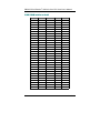
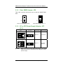
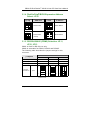
1
SBC8176 Dual Pentium II/III PCI/ISA CPU Card User’s Manual Disclaimers ! " ! # !! ! Copyright 2000 by AXIOM Technology Co., Ltd. All rights reserved. March 2000, Version A3 Printed in Taiwan ii ESD Precautions Integrated circuits on computer boards are sensitive to static electricity. To avoid damaging chips from electrostatic discharge, observe the following precautions: ! Do not remove boards or integrated circuits from their anti-static packaging until you are ready to install them. ! Before handling a board or integrated circuit, touch an unpainted portion of the system unit chassis for a few seconds. This helps to discharge any static electricity on your body. ! Wear a wrist-grounding strap, available from most electronic component stores, when handling boards and components. Trademarks Acknowledgments AXIOM is a trademark of AXIOM Technology Co., Ltd. Award is a registered trademark of Award Software International, Inc. IBM, PS/2 are trademarks of International Business Machines Corporation. Intel and Pentium are registered trademarks of Intel Corporation. Microsoft Windows is a registered trademark of Microsoft Corporation. Other brand names and trademarks are the properties and registered brands of their respective owners. iii Unpacking After unpacking the CPU card, check and see if the following items are included and in good condition. If any of the items is missing or damaged, notify your dealer immediately. ! SBC8176 Dual Pentium II/III PCI/ISA CPU Card x 1 ! User’s Manual and Warranty Card x 1 ! IDE Ribbon Cable x 1 ! PS/2 Keyboard Adapter Cable x 1 ! Floppy Ribbon Connector x 1 ! One serial port ribbon cable and one parallel port attached to a mounting bracket x 1 set ! Thermistor with cables x 3 ! Termination board x 1 ! Diskette containing System Hardware Doctor Utility x 2 Make sure that all of the items listed above are present. What To Do If There Is A Problem If there are damaged or missing parts, contact your supplier and/or dealer immediately. Do not attempt to apply power to the board if there is damage to any of its components. iv Table of Contents Chapter 1 Introduction 1.1 1.2 1.3 1.4 1.5 General Description .............................. 1 Features ................................................ 2 Specifications ........................................ 2 Intelligence ........................................... 4 Board Dimensions ................................... 5 Chapter 2 Installation 2.1 CPU Installation ................................... 7 2.1.1 2.1.2 Single Processor Installation ..................................... 8 Dual Processor Installation ...................................... 8 2.2 Memory Installation .............................. 8 16MB SDRAM installed on Bank0 ............................... 9 32MB SDRAM installed on Bank0 ..............................10 64MB SDRAM installed on Bank0 ..............................11 128MB SDRAM installed on Bank0.............................12 Chapter 3 Jumpers and Connectors 3.1 Jumpers ................................................ 13 3.1.1 CPU Settings.................................................... 15 3.1.1.1 3.1.1.2 3.1.1.3 3.1.2 3.1.3 3.1.4 3.1.5 3.1.6 3.1.7 Core Frequency to System Bus Multiplier Configuration: JP4 ............................... 15 System Bus Freuency Setting: JP6 ......... 15 CPU Frequency Reference Table .......... 16 Clear CMOS Jumper: JP8 ................................... AT or ATX Power Supply Selector: JP7, JP15 ......... DiskOnChip BIOS Expansion Address Select: JP10 .. RS232/422/485 (COM2) Selection: JP11, JP12, JP13 ............................................................. SMI Selector: JP5 ............................................. Watchdog Timer Selector: JP9 .............................. 18 18 19 19 20 20 3.2 Connectors .......................................... 21 3.2.1 Front Bezel Connector: CN3................................. 23 Speaker: Pins 2, 4, 6, 8 ....................................... 23 Power LED and Keylock: Pins 1, 3, 5, 7, 9 ............ 24 SMI/Hardware Switch: Pins 11 and 12 .................. 24 Reset Switch: Pins 17 and 18 ............................... 24 Hard Disk Drive LED Connector: Pins 19 and 20 ................................................... 25 Table of Contents v 3.2.2 EIDE Connectors: CN7, CN8............................... 25 CN7: Primary IDE Connector ............................... 25 CN8: Secondary IDE Connector .......................... 26 3.2.3 3.2.4 3.2.5 3.2.6 3.2.7 3.2.8 3.2.9 3.2.10 3.2.11 3.2.12 3.2.13 3.2.14 Floppy Drive Connector: CN9............................... Parallel Port Connector: CN11.............................. COM1 Serial Port: CN17................................... COM2 Serial Port: CN16................................... Internal Keyboard Connector: CN10 Internal Mouse Connector: CN14 ............................................. External ATX Power Connector: CN15 ................... External PS/2 Keyboard and Mouse Connector: CN18............................................................ CPUI Fan Power Connector: CN1 .......................... CPUII Fan2 Connector: CN2................................ USB Connector: CN13 ....................................... IrDA Connector: CN12 ...................................... Temperature Thermistor Connectors: CN4, CN5, CN6 ............................................. 27 28 28 29 29 30 30 30 30 31 31 32 Chapter 4 BIOS Configuration 4.1 BIOS Introduction ................................ 33 4.2 BIOS Setup ........................................... 33 4.3 Standard CMOS Setup .......................... 35 4.4 BIOS Features Setup ............................ 38 4.5 Chipset Features Setup ....................... 42 4.6 Power Management Setup..................... 45 4.7 PNP/PCI Configuration ......................... 48 4.8 Load BIOS Defaults ............................. 49 4.9 Load Setup Defaults ............................ 50 4.10 Integrated Peripherals ....................... 51 4.11 Supervisor / User Password................. 53 4.12 IDE HDD Auto Detection ....................... 54 4.13 Save & Exit Setup ................................. 55 4.14 Exit Without Saving ............................. 56 Chapter 5 System Hardware Doctor 5.1 System Hardware Doctor Installation 57 5.2 Launching the System Hardware Doctor Utility ...................................... 58 vi Table of Contents Appendix A Watchdog Timer Configuration Using the Watchdog Function ..................... 61 Appendix B Appendix C Table of Contents I/O Port Address Map Interrupt Inter rupt Request Lines (IRQ) vii viii SBC8176 Dual Pentium II/III All-in-One CPU Card User’s Manual Chapter 1 Introduction 1.1 General Description The SBC8176 is a Dual Pentium II/III industrial CPU card based on Intels 440BX chipset and is fully designed for harsh industrial environment. It features two Slot 1 processor connectors that are compatible with Pentium II/III processors. This card accommodates up to 512MB of unbuffered SDRAMs or 1GB of buffer SDRAM configurations. The SBC8176 comes with W inbonds W 83781D hardware monitoring device that monitors system/CPU temperatures, system voltages, and CPU/chassis fan speeds, preventing system crashes by warning the user of adverse conditions. The power management feature provides power savings by slowing down the CPU clock, turning OFF the monitor screen and stopping the HDD spindle motor. Introduction 1 SBC8176 Dual Pentium II/III All-in-One CPU Card User’s Manual 1.2 Features " CPU Speed 266~500MHz, Intel Pentium II/III " Bus Speed 66MHz/100MHz " Intel 440BX AGPset " Up to 512MB of unbuffered SDRAMs or 1GB of buffered SDRAM system memory, ECC function supported " 16-level software programmable watchdog timer with temperature and time intervals from 0.5 to 1000 seconds " High speed bi-directional SPP/ECP/EPP parallel port " Hardware Monitoring " Win 95/98 shut-off 1.3 Specifications " Processor Socket: Dual Slot 1 connector " Processor: ! Intel Pentium II 333MHz (66MHz / Deschutes) ! Intel Pentium II 300/350/400/450/500 MHz (100MHz / Deschutes) ! Intel Pentium III 450/500/550/600 MHz (Katmai) ! Intel Pentium III 600E/650E/700E MHz (Coppermine) " Chipset: Intel 440BX AGPset with PCI EIDE " Secondary Cache: CPU integrated " Memory Sockets: ! Four 168-pin DIMM sockets ! Memory types: SDRAM (Synchronous DRAM) NOTE: 2 Only SDRAM modules that support SPD (Serial Presence Detect) should be used. Use PC100 modules when running 100MHz CPU bus speed and use PC66/PC100 modules when running 66MHz CPU bus speed. Introduction SBC8176 Dual Pentium II/III All-in-One CPU Card User’s Manual " BIOS: Award BIOS, PnP support ! FLASH EEPROM (256KB) for BIOS update ! ISA Plug and Play (PnP) extension ! Power management " Multi I/O: Winbond W83977TF " Parallel Port: One high-speed parallel port, SPP/EPP/ECP mode " Serial Port: Two 16550 UART compatible ports with COM1 as RS232 and COM2 jumper configurable as RS232/422/485 " Enhanced IDE: ! Two EIDE interfaces for up to four devices ! Supports PIO Mode 3/4, DMA Mode 0~2, and Ultra DMA/33 IDE Hard Disk and ATAPI CD-ROM " FDD Interface: Two floppy drives (360KB, 720KB, 1.2MB, 1.44MB, 2.88MB, LS-120) " USB Interface: Two USB box-header connectors, compliant with USB Specification Rev. 1.0 " DiskOnChip : The M-Systems flask disk supports system boot and storage capacity from 2MB to 72MB. " Real Time Clock: DS12887A or STM48T86 " Watchdog Timer: Generates a system reset 16-level software programmable time and temperature interval from 0.5 to 1000 seconds " Green Function: Power management via BIOS, activated through mouse/keyboard movement " Keyboard and Mouse Connectors: ! One mini-DIN connector supporting external keyboard and mouse ! One 5-pin connector supporting internal keyboard ! One 5-pin connector supporting internal mouse " IrDA Interface: Box-header connector for the optional IrDA external connector Introduction 3 SBC8176 Dual Pentium II/III All-in-One CPU Card User’s Manual " PICMG Compliance: Fully compliant to PICMG standards " Power Consumption: ! +5V @16A, +12V @1.5A (max.) (Dual Pentium II 400MHz, 128MB SDRAM) " Environmental and Mechanical: ! Temperature: 0°C to 60°C ! Humidity: 5% to 95% ! Dimensions: 338.2mm x 121.9mm 1.4 Intelligence " Windows 95 shut-off: Allows shut-off control from within Windows 95 and through an ATX power supply. " Year 2000 Compliant BIOS: The onboard Award BIOS is Year 2000 Compliant and will pass software applications that have the tendency to invoke INT1AH function 04H such as year2000.exe utility released by NSTL. " Temperature Monitoring and Alert (optional): Two sensor connectors on the SBC8176 monitors the CPU and system temperature. When temperature exceeds the safe heat level, this feature alerts the user through the speaker or buzzer. 4 Introduction SBC8176 Dual Pentium II/III All-in-One CPU Card User’s Manual Board Dimensions COM1 20.00 338.24 COM2 25.06 1.5 121.92 SBC8176 Board Dimensions Introduction 5 SBC8176 Dual Pentium II/III All-in-One CPU Card User’s Manual 6 SBC8176 Dual Pentium II/III All-in-One CPU Card User’s Manual Chapter 2 Installation This chapter provides information on how to configure the jumpers and connectors on the SBC8176 in order to set up a workable system. 2.1 CPU Installation The SBC8176 Industrial CPU card supports Dual Slot 1 connector/processor sockets for Pentium II/III processors. This connector secures the installation of the Pentium II/III processor, ensuring the proper installation of the CPU. Before installing the Pentium II/III processor into the Slot 1 connector, ensure that the CPU fan is securely installed. After doing so, insert the processor into the Slot 1 connector. Locking mechanism on both sides of the Slot 1 connector will click and secure the Pentium II/III processor. To uninstall the Pentium II/III processor, simply push the locking mechanism on both sides simultaneously and remove the Pentium II/III processor. No tools are needed. CAUTION: When installing two Pentium II/III processors onboard the SBC8176, make sure that both processors have identical clock speeds. Mixed combinations are not allowed. WARNING: SBC8176 supports installation of a single or dual Pentium II/III processor. When using only a single Pentium II/III processor, install only on CPUI Slot1 connector. Do not attempt to mount the Pentium II/III processor into the CPU2 Slot 2 connector! Installation 7 SBC8176 Dual Pentium II/III All-in-One CPU Card User’s Manual 2.1.1 Single Processor Installation W hen configuring the SBC8176 for single processor setting, install the processor into CPUI slot. Refer to the illustration on Section 3.2 for the actual location of CPUI slot. After installing the CPU into the CPUI slot, mount the termination board into CPUII slot. 2.1.2 Dual Processor Installation W hen configuring the SBC8176 for dual processor setting, install the processors into CPUI and CPUII slots. Make sure that both processors have identical frequency speed. 2.2 Memory Installation The SBC8176 Industrial CPU Card supports four 168-pin DIMM (Dual In-line Memory Module) sockets for a maximum total memory of 512MB unbuffered SDRAMs or 1GB buffer SDRAMs. The memory modules can come in sizes of 16MB, 32MB, 64MB, 128MB and 256MB (for buffer type) SDRAMs. W hen populating the DIMM sockets, DIMM1,2,3 or DIMM4 bank can be populated first. Refer to the following table on how to configure the memory. NOTE: 8 Use SDRAM modules with PC100 specification when running 100MHz CPU bus speed. With 66MHz CPU bus speed, SDRAM modules with PC66 or PC100 specification can be used. You have to install the Pentium II/III processor before installing the memory modules. Installation SBC8176 Dual Pentium II/III All-in-One CPU Card User’s Manual 16MB SDRAM installed on Bank0 Bank0 Bank1 Bank2 Bank 3 16MB 16MB 16MB 16MB 16MB 16MB 16MB 16MB 16MB 16MB 16MB 16MB 16MB 16MB 16MB 16MB 16MB 16MB 16MB 16MB 16MB 16MB 16MB 16MB 16MB 16MB 16MB 16MB 16MB 16MB 16MB ------------------------8MB 8MB 8MB 8MB 8MB 16MB 16MB 16MB 16MB 16MB 32MB 32MB 32MB 32MB 32MB 64MB 64MB 64MB 64MB 64MB 128MB 128MB 128MB 128MB 128MB ----8MB 16MB 32MB 64MB 128MB 8MB 16MB 32MB 64MB 128MB 8MB 16MB 32MB 64MB 128MB 8MB 16MB 32MB 64MB 128MB 8MB 16MB 32MB 64MB 128MB 8MB 16MB 32MB 64MB 128MB ----8MB 16MB 32MB 64MB 128MB 8MB 16MB 32MB 64MB 128MB 8MB 16MB 32MB 64MB 128MB 8MB 16MB 32MB 64MB 128MB 8MB 16MB 32MB 64MB 128MB 8MB 16MB 32MB 64MB 128MB Installation Total 16MB 32MB 48MB 80MB 144MB 272MB 40MB 56MB 88MB 152MB 280MB 48MB 64MB 96MB 160MB 288MB 64MB 80MB 112MB 176MB 304MB 96MB 112MB 144MB 208MB 336MB 160MB 176MB 208MB 272MB 400MB 9 SBC8176 Dual Pentium II/III All-in-One CPU Card User’s Manual 32MB SDRAM installed on Bank0 10 Bank0 Bank1 Bank2 Bank 3 32MB 32MB 32MB 32MB 32MB 32MB 32MB 32MB 32MB 32MB 32MB 32MB 32MB 32MB 32MB 32MB 32MB 32MB 32MB 32MB 32MB 32MB 32MB 32MB 32MB 32MB 32MB 32MB 32MB 32MB 32MB ------------------------8MB 8MB 8MB 8MB 8MB 16MB 16MB 16MB 16MB 16MB 32MB 32MB 32MB 32MB 32MB 64MB 64MB 64MB 64MB 64MB 128MB 128MB 128MB 128MB 128MB ----8MB 16MB 32MB 64MB 128MB 8MB 16MB 32MB 64MB 128MB 8MB 16MB 32MB 64MB 128MB 8MB 16MB 32MB 64MB 128MB 8MB 16MB 32MB 64MB 128MB 8MB 16MB 32MB 64MB 128MB ----8MB 16MB 32MB 64MB 128MB 8MB 16MB 32MB 64MB 128MB 8MB 16MB 32MB 64MB 128MB 8MB 16MB 32MB 64MB 128MB 8MB 16MB 32MB 64MB 128MB 8MB 16MB 32MB 64MB 128MB Total 32MB 48MB 64MB 96MB 160MB 288MB 56MB 72MB 104MB 168MB 296MB 64MB 80MB 112MB 176MB 304MB 80MB 96MB 128MB 192MB 320MB 112MB 128MB 160MB 224MB 352MB 176MB 192MB 224MB 288MB 416MB Installation SBC8176 Dual Pentium II/III All-in-One CPU Card User’s Manual 64MB SDRAM installed on Bank0 Bank0 Bank1 Bank2 Bank 3 64MB 64MB 64MB 64MB 64MB 64MB 64MB 64MB 64MB 64MB 64MB 64MB 64MB 64MB 64MB 64MB 64MB 64MB 64MB 64MB 64MB 64MB 64MB 64MB 64MB 64MB 64MB 64MB 64MB 64MB 64MB ------------------------8MB 8MB 8MB 8MB 8MB 16MB 16MB 16MB 16MB 16MB 32MB 32MB 32MB 32MB 32MB 64MB 64MB 64MB 64MB 64MB 128MB 128MB 128MB 128MB 128MB ----8MB 16MB 32MB 64MB 128MB 8MB 16MB 32MB 64MB 128MB 8MB 16MB 32MB 64MB 128MB 8MB 16MB 32MB 64MB 128MB 8MB 16MB 32MB 64MB 128MB 8MB 16MB 32MB 64MB 128MB ----8MB 16MB 32MB 64MB 128MB 8MB 16MB 32MB 64MB 128MB 8MB 16MB 32MB 64MB 128MB 8MB 16MB 32MB 64MB 128MB 8MB 16MB 32MB 64MB 128MB 8MB 16MB 32MB 64MB 128MB Installation Total 64MB 80MB 96MB 128MB 192MB 320MB 88MB 104MB 136MB 200MB 328MB 96MB 112MB 144MB 208MB 336MB 112MB 128MB 160MB 224MB 352MB 144MB 160MB 192MB 256MB 384MB 208MB 224MB 256MB 320MB 448MB 11 SBC8176 Dual Pentium II/III All-in-One CPU Card User’s Manual 128MB SDRAM installed on Bank0 12 Bank0 Bank1 Bank2 Bank 3 128MB 128MB 128MB 128MB 128MB 128MB 128MB 128MB 128MB 128MB 128MB 128MB 128MB 128MB 128MB 128MB 128MB 128MB 128MB 128MB 128MB 128MB 128MB 128MB 128MB 128MB 128MB 128MB 128MB 128MB 128MB ------------------------8MB 8MB 8MB 8MB 8MB 16MB 16MB 16MB 16MB 16MB 32MB 32MB 32MB 32MB 32MB 64MB 64MB 64MB 64MB 64MB 128MB 128MB 128MB 128MB 128MB ----8MB 16MB 32MB 64MB 128MB 8MB 16MB 32MB 64MB 128MB 8MB 16MB 32MB 64MB 128MB 8MB 16MB 32MB 64MB 128MB 8MB 16MB 32MB 64MB 128MB 8MB 16MB 32MB 64MB 128MB ----8MB 16MB 32MB 64MB 128MB 8MB 16MB 32MB 64MB 128MB 8MB 16MB 32MB 64MB 128MB 8MB 16MB 32MB 64MB 128MB 8MB 16MB 32MB 64MB 128MB 8MB 16MB 32MB 64MB 128MB Total 128MB 144MB 160MB 192MB 256MB 384MB 152MB 168MB 200MB 264MB 392MB 160MB 176MB 208MB 272MB 400MB 176MB 192MB 224MB 288MB 416MB 208MB 224MB 256MB 320MB 448MB 272MB 288MB 320MB 384MB 512MB Installation SBC8176 Dual Pentium II/III All-in-One CPU Card User’s Manual Chapter 3 Jumpers and Connectors 3.1 Jumpers The jumpers on the SBC8176 allow you to configure your CPU card according to the needs of your applications. If you have doubts about the best jumper configuration for your needs, contact your dealer or sales representative. The following table lists the connectors on SBC8176 and their respective functions. Jumper JP4, JP6 JP5 JP7, JP15 JP8 JP9 JP10 JP11, JP12, JP13 NOTE: Description CPU Frequency Selector SMI Selector AT or ATX Power Supply Selector Clear CMOS Jumper Watchdog Timer Selector DiskOnChip BIOS Expansion Address Select RS232/422/485 (COM2) Selection Jumpers JP1and JP1 JP2 (All open default) are for manufacturer testing use only. Jumper JP3 is not used. Short 1-2 is the default setting of JP16. Jumpers and Connectors 13 SBC8176 Dual Pentium II/III All-in-One CPU Card User’s Manual JP16 JP15 1 FDD 2 JP10 1 5 7 1 5 1 1 JP11 JP12 JP13 DiskOnChipTM JP9 JP8 RTC JP6 CLK 1 1 2 1 JP7 2 2 1 JP4 JP5 IDE1 PIIX4 BIOS IDE2 I/O KB JP1 JP2 443BX A2 A1 SBC8176 Jumper Locations 14 Jumpers and Connectors SBC8176 Dual Pentium II/III All-in-One CPU Card User’s Manual 3.1.1 CPU Settings W hen a new CPU is to be installed, only jumpers JP4 and JP6 need to be adjusted. Multiplication of Core Frequency to System Bus Frequency 1/2.0 1/2.5 1/3.0 1/3.5 1/4.0 1/4.5 1/5.0 1/5.5 1/6.0 1/6.5 1/7.0 1/7.5 1/8.0 JP4 Setting Short Short Short Short Short Short Short Short Short Short Short Short Short 1-2, 1-2, 1-2, 1-2, 3-4, 3-4, 5-6, 7-8 1-2, 1-2, 1-2, 1-2 3-4, 3-4, 3-4, 5-6, 7-8 5-6, 7-8 7-8 5-6, 7-8 7-8 7-8 7-8 3-4, 5-6 3-4 5-6 5-6 System Bus Frequency 66.6MHz 100MHz Jumpers and Connectors JP6 Setting Short 1-2 Short 2-4 15 SBC8176 Dual Pentium II/III All-in-One CPU Card User’s Manual ! "#$ The following table serves as a reference on the correct jumper settings that match a few selected CPU frequencies. CPU Type CPU Frequency Deschutes 66MHz Host Clock CPU 5x 66.6MHz 333MHz JP4 Setting 2 JP6 Setting 8 2 8 1 7 1 7 2 8 2 8 1 7 1 7 2 8 2 8 1 7 1 7 2 8 2 8 1 7 1 7 2 8 2 8 1 7 1 7 2 8 2 8 1 7 1 7 3 x 100MHz 300MHz PII Deschutes 100MHz Host Clock CPU 3.5 x 100MHz 350MHz 4 x 100MHz 400MHz 4.5 x 100MHz 450MHz 5 x 100MHz 500MHz Continued . . . . . 16 Jumpers and Connectors SBC8176 Dual Pentium II/III All-in-One CPU Card User’s Manual CPU Type CPU Frequency JP4 Setting 2 8 JP6 Setting 2 8 4.5 x 100MHz 450MHz PIII Katmai 100MHz Host Clock CPU 1 7 1 7 2 8 2 8 1 7 1 7 2 8 2 8 5.0 x 100MHz 500MHz 5.5 x 100MHz 550MHz 1 7 1 7 2 8 2 8 1 7 1 7 2 8 2 8 1 7 1 7 2 8 2 8 1 7 1 7 2 8 2 8 1 7 1 7 6.0 x 100MHz 600MHz 6.0 x 100MHz 600E PIII Coppermine 100MHz Host Clock CPU 6.5 x 100MHz 650E 7.0 x 100MHz 700E Jumpers and Connectors 17 SBC8176 Dual Pentium II/III All-in-One CPU Card User’s Manual 3.1.2 Clear CMOS Jumper: JP8 This 2-pin connector allows the user to clear the CMOS RAM data. 1 1 2 2 Normal operation: Open (default) 3.1.3 AT or ATX Power Supply Selector: JP7, JP15 JP7 2 JP15 1 5 2 6 1 1 NOTE: Setting Function Short 2-3 ATX Power Short 1-2 AT Power (default) 6 1 18 Clear CMOS Contents: Short 1-2 2 2 3 3 5 When configured for the ATX power supply, your system must have a special backplane that supports an ATX power supply. Jumpers and Connectors SBC8176 Dual Pentium II/III All-in-One CPU Card User’s Manual 3.1.4 DiskOnChip BIOS Expansion Address Select: JP10 JP10 3 Address JP10 1 3 D8000-D7FFF 4 3 D4000-DBFFF 2 4 2 1 3 1 D0000-D3FFF (default) 4 Address 1 DC000-DFFFF 4 2 2 3.1.5 RS232/422/485 (COM2) Selection: JP11, JP12, JP13 COM1 is fixed for RS-232 use only. COM2 is selectable for RS232, RS-422 and RS-485. The following table describes the jumper settings for this connector. COM2 Function Jumpers JP11 JP12 JP13 Jumper Illustration RS-232 RS-422 RS-485 Short 1-2 Short 3-5, 4-6 Short 3-5, 4-6 Short 3-4 Short 1-3, 2-4 Short 1-3, 2-4 Short 5-6, 7-8 Short 1-3, 2-4 Short 1-3, 2-4 1 2 1 2 1 2 7 8 7 8 7 8 JP11 Continued . . . . . Jumpers and Connectors 19 SBC8176 Dual Pentium II/III All-in-One CPU Card User’s Manual Jumpers COM2 Function RS-232 RS-422 RS-485 1 2 1 2 1 2 5 6 5 6 5 6 1 2 1 2 1 2 5 6 5 6 5 6 JP12 Jumper Illustration 3.1.6 JP13 SMI Selector: JP5 Options 3.1.7 Setting CPU SMI comes from IOAPIC Short 1-2 CPU SMI comes from PIIX4 (default) Short 2-3 JP5 1 2 3 1 2 3 Watchdog Timer Selector: JP9 Options Setting JP9 1 Watchdog generates NMI Short 1-2 2 3 1 Watchdog generates Reset Short 2-3 2 3 Default: Open (Watchdog function disabled) 20 Jumpers and Connectors SBC8176 Dual Pentium II/III All-in-One CPU Card User’s Manual 3.2 Connectors The connectors on the SBC8176 allows you to connect external devices such as keyboard, floppy disk drives, hard disk drives, printers, etc. The following table lists the connectors on SBC8176 and their respective functions. Connectors CPUI FAN Connector CPUII FAN Connector Front Bezel Connector System Temperature Connector CPUI Temperature Connector CPUII Temperature Connector EIDE Connectors Floppy Drive Connector Internal Keyboard Connector Parallel Port Connector IrDA Connector USB Connectors Internal PS/2 Mouse Connector External ATX Power Connector COM2 Serial Port COM1 Serial Port External PS/2 Keyboard/Mouse Connector Jumpers and Connectors Label CN1 CN2 CN3 CN4 CN5 CN6 CN7, CN8 CN9 CN10 CN11 CN12 CN13 CN14 CN15 CN16 CN17 CN18 21 22 CPUII 443BX CLK PIIX4 BIOS USB CN13 CN18: KB & Mouse IR CN12 DiskOnChipTM RTC CN14: Mouse 1 CN17 COM1 CN10: Keyboard 1 1 CN16 COM2 CN2 1 CN6 Front Bezel CPUI Fan CPUI Temperature System Temperature CPUII Temperature CPUII Fan CN9 FDD PRINTER CN4 CN3: CN1: CN5: CN4: CN6: CN2: CPUI CN8 IDE2 CN7 IDE1 CN15: Ext. ATX Power CN5 CN1 19 1 CN3 A2 A1 1 2 SBC8176 Dual Pentium II/III All-in-One CPU Card User’s Manual I/O KB SBC8176 Connector Locations Jumpers and Connectors SBC8176 Dual Pentium II/III All-in-One CPU Card User’s Manual 3.2.1 Front Bezel Connector: CN3 The front bezel of the case has a control panel that provides light indication of the computer activities and switches to change the computer status. CN3 is a 20-pin header that provides interfaces for the following functions. 1 2 Speaker Power LED & Keylock SMI / Hardware Switch Reset Switch Hard Disk Drive LED 19 20 %&& &' This connector provides an interface to a speaker for audio tone generation. An 8-ohm speaker is recommended. 2 4 6 8 Pin # 6 Speaker out Short 2-3 for Internal Buzzer 8 +5V 2 4 Jumpers and Connectors Signal Name 23 SBC8176 Dual Pentium II/III All-in-One CPU Card User’s Manual ()*+,-%&&.&/&0 The power LED indicates the status of the main power switch. The keylock switch, when closed, will disable the keyboard function. Pin # Signal Name Power LED (+) No connector Ground Keylock Ground 1 3 5 1 3 5 7 9 7 9 123,((4, This connector supports the "Green Switch" from the control panel, which, when pressed, will force the system into the power-saving mode immediately. Pin # 12 11 12 1 3 5 7 Signal Name Ground Sleep 9 11 "(4/,' The reset switch allows the user to reset the system without turning the main power switch OFF and then ON. Orientation is not required when making a connection to this header. 18 20 1 24 17 19 Jumpers and Connectors SBC8176 Dual Pentium II/III All-in-One CPU Card User’s Manual 3,+%+5)*+0,6 This connector connects to the hard drive activity LED on control panel. This LED will flash when the HDD is being accessed. Pin # 20 19 20 1 3.2.2 Signal Name LED(-) LED(+) 19 EIDE Connectors: CN7, CN8 7/1+* Signal Name CN7 Reset IDE Host data 7 Host data 6 Host data 5 Host data 4 Host data 3 Host data 2 Host data 1 Host data 0 Ground DRQ0 Host IOW Host IOR IOCHRDY DACK0 IRQ14 Address 1 Address 0 Chip select 0 Activity Jumpers and Connectors Pin # Pin # 1 3 5 7 9 11 13 15 17 19 21 23 25 27 29 31 33 35 37 39 2 4 6 8 10 12 14 16 18 20 22 24 26 28 30 32 34 36 38 40 Signal Name Ground Host data 8 Host data 9 Host data 10 Host data 11 Host data 12 Host data 13 Host data 14 Host data 15 Key Ground Ground Ground Host ALE Ground No connector No connector Address 2 Chip select 1 Ground 25 SBC8176 Dual Pentium II/III All-in-One CPU Card User’s Manual 7',1+* Signal Name CN8 26 Reset IDE Host data 7 Host data 6 Host data 5 Host data 4 Host data 3 Host data 2 Host data 1 Host data 0 Ground DRQ1 Host IOW Host IOR IOCHRDY DACK1 IRQ15 Address 1 Address 0 Chip select 0 Activity Pin # Pin # 1 3 5 7 9 11 13 15 17 19 21 23 25 27 29 31 33 35 37 39 2 4 6 8 10 12 14 16 18 20 22 24 26 28 30 32 34 36 38 40 Signal Name Ground Host data 8 Host data 9 Host data 10 Host data 11 Host data 12 Host data 13 Host data 14 Host data 15 Key Ground Ground Ground Host ALE Ground No connector No connector Address 2 Chip select 1 Ground Jumpers and Connectors SBC8176 Dual Pentium II/III All-in-One CPU Card User’s Manual 3.2.3 Floppy Drive Connector: CN9 CN9 is a 34-pin header and supports disk drives of up to 2.88MB. Signal Name CN9 Ground Ground Ground Ground Ground Ground Ground Ground Ground Ground Ground Ground Ground Ground Ground Ground Ground Jumpers and Connectors Pin # Pin # 1 3 5 7 9 11 13 15 17 19 21 23 25 27 29 31 33 2 4 6 8 10 12 14 16 18 20 22 24 26 28 30 32 34 Signal Name RM/LC No connector No connector Index Motor enable 0 Drive select 1 Drive select 0 Motor enable 1 Direction Step Write data Write gate Track 00 Write protect Read data Side 1 select Diskette change 27 SBC8176 Dual Pentium II/III All-in-One CPU Card User’s Manual 3.2.4 Parallel Port Connector: CN11 The following table describes the pin out assignments of this connector. 1 25 2 Signal Name Pin # Pin # Line printer strobe PD0, parallel data 0 PD1, parallel data 1 PD2, parallel data 2 PD3, parallel data 3 PD4, parallel data 4 PD5, parallel data 5 PD6, parallel data 6 PD7, parallel data 7 ACK, acknowledge Busy Paper empty Select 1 3 5 7 9 11 13 15 17 19 21 23 25 2 4 6 8 10 12 14 16 18 20 22 24 26 Signal Name AutoFeed Error Initialize Select Ground Ground Ground Ground Ground Ground Ground Ground Ground 26 CN11 3.2.5 COM1 Serial Port: CN17 CN17, a DB-9 connector, is an onboard serial port of the SBC8176. The following table shows the pin assignments of this connector. Pin # CN17 28 1 2 3 4 5 6 7 8 9 Signal Name DCD, Data carrier detect RXD, Receive data TXD, Transmit data DTR, Data terminal ready GND, ground DSR, Data set ready RTS, Request to send CTS, Clear to send RI, Ring indicator Jumpers and Connectors SBC8176 Dual Pentium II/III All-in-One CPU Card User’s Manual 3.2.6 COM2 Serial Port: CN16 CN16, a DB-9 connector, is the onboard COM2 serial port of the SBC8176. The following table shows its pin assignments. Signal Name Pin # RS-232 DCD RX TX DTR GND DSR RTS CTS RI 1 2 3 4 5 6 7 8 9 CN16 R2-422 RS-485 TXTX+ RX+ RXGND No connector No connector No connector No connector DATADATA+ No connector No connector GND No connector No connector No connector No connector 3.2.7 Internal Keyboard Connector: CN10 Internal Mouse Connector: CN14 1 Pin # 1 2 3 CN10 5 1 4 5 Pin # 1 2 3 CN14 5 Jumpers and Connectors 4 5 Signal Name Keyboard clock Keyboard data PG GND Vcc Signal Name Mouse clock Mouse data PG GND Vcc 29 SBC8176 Dual Pentium II/III All-in-One CPU Card User’s Manual 3.2.8 External ATX Power Connector: CN15 1 Pin # Signal Name 1 SMI GND ATX Power Button GND PS-ON (soft ON/OFF); to ATX power supply 5V SB (standby +5V); from ATX power supply 2 3 6 CN15 4 5 6 3.2.9 External PS/2 Keyboard and Mouse Connector: CN18 Pin # Signal Name Keyboard data Mouse clock GND 5V Keyboard clock Mouse data 1 2 3 4 5 6 CN18 3.2.10 CPUI Fan Power Connector: CN1 CN1 is a 3-pin header for the CPU fan. The fan must be a 12V fan. Pin # 3 2 1 1 2 3 Signal Name Ground +12V Rotation 3.2.11 CPUII Fan2 Connector: CN2 CN2 is a 3-pin header for the chassis fan. The fan must be a 12V fan. Pin # 3 2 30 1 1 2 3 Signal Name Rotation +12V Ground Jumpers and Connectors SBC8176 Dual Pentium II/III All-in-One CPU Card User’s Manual 3.2.12 USB Connector: CN13 The following table shows the pin outs of the USB connector. 1 2 CN17 Pin # 1, 2 3 4 5 6 7, 8 9, 10 9 Signal Name USB Vcc USB0USB1USB0+ USB1USBGND Reserved 10 CN13 3.2.13 IrDA Connector: CN12 This connector is used for an IrDA connection for wireless communication. 1 2 Pin # 1 2 3 4 5 6 7 8 9 10 9 Signal Name +5V No connector Flr RX Clr RX Ir RX 5VSB GND No connector Ir TX No connector 10 CN12 Jumpers and Connectors 31 SBC8176 Dual Pentium II/III All-in-One CPU Card User’s Manual 3.2.14 Temperature Thermistor Connectors: CN4, CN5, CN6 Connector CN4 2 1 CN5 Pin1: GND Pin2: Thermistor NOTE: 32 CN6 Function Thermistor connector for system temperature Thermistor connector for CPUI temperature Thermistor connector for CPUII temperature The SBC8176 can use any thermistor with 10k Ω +/2.5% and B(25/85) value equal to 3435k +/-2%. Jumpers and Connectors SBC8176 Dual Pentium II/III All-in-One CPU Card User’s Manual Chapter 4 BIOS Configuration Chapter 3 describes the different settings available in the Award BIOS that comes with the SBC8176 CPU card. Also contained here are instructions on how to set up the BIOS configuration. 4.1 BIOS Introduction The Award BIOS (Basic Input/Output System) installed in your computer systems ROM supports Intel Pentium II/III processors in a standard IBM-AT compatible I/O system. The BIOS provides critical low-level support for standard devices such as disk drives, serial and parallel ports. It also adds virus and password protection as well as special support for detailed fine-tuning of the chipset controlling the entire system. 4.2 BIOS Setup The Award BIOS provides a Setup utility program for specifying the system configurations and settings. The BIOS ROM of the system stores the Setup utility. W hen you turn ON the computer, the Award BIOS is immediately activated. Pressing the <Del> key immediately allows you to enter the Setup utility. If you are a little bit late pressing the <Del> key, POST (Power On Self Test) will continue with its test routines, thus preventing you from invoking the Setup. If you still wish to enter Setup, restart the system by pressing the Reset button or simultaneously pressing the <Ctrl>, <Alt> and <Delete> keys. You can also restart by turning the system OFF and back ON again. The following message will appear on the screen: Press <DEL> to Enter Setup In general, you press the arrow keys to highlight items, <Enter> to select, the <PgUp> and <PgDn> keys to change entries, <F1> for help and <Esc> to quit. BIOS Configuration 33 SBC8176 Dual Pentium II/III All-in-One CPU Card User’s Manual W hen you enter the Setup utility, the Main Menu screen will appear on the screen. The Main Menu allows you to select from various setup functions and exit choices. ROM PCI/ISA BIOS CMOS SETUP UTILITY AWARD SOFTWARE, INC. STANDARD CMOS SETUP INTEGRATED PERIPHERALS BIOS FEATURES SETUP SUPERVISOR PASSW ORD CHIPSET FEATURES SETUP USER PASSW ORD POW ER MANAGEMENT SETUP IDE HDD AUTO DETECTION PNP/PCI CONFIGURATION SAVE & EXIT SETUP LOAD BIOS DEFAULTS EXIT W ITHOUT SAVING LOAD SETUP DEFAULTS ESC : Quit # $ % & : Select Item F10 : Save & Exit Setup (Shift) F2 : Change Color Time, Date, Hard Disk Type The section below the setup items of the Main Menu displays the control keys for this menu. Another section located at the bottom of the Main Menu, just below the control keys section, displays information on the currently highlighted item in the list. NOTE: If you find that your computer cannot boot after making and saving system changes with Setup, the Award BIOS, via its built-in override feature, resets your system to the CMOS default settings. W e strongly recommend that you avoid making any changes to the chipset defaults. These defaults have been carefully chosen by both Award and your system manufacturer to provide the absolute maximum performance and reliability. 34 BIOS Configuration SBC8176 Dual Pentium II/III All-in-One CPU Card User’s Manual 4.3 Standard CMOS Setup Standard CMOS Setup allows you to record some basic hardware configurations in your computer system and set the system clock and error handling. If the motherboard is already installed in a working system, you will not need to select this option. You will need to run the Standard CMOS option, however, if you change your system hardware configurations, the onboard battery fails, or the configuration stored in the CMOS memory was lost or damaged. ROM PCI/ISA BIOS STANDARD CMOS SETUP AWARD SOFTWARE, INC. Date (mm:dd:yy) : W ed, Mar 4 1998 Time (hh:mm:ss) : 00 : 00 : 00 HARD DISKS TYPE SIZE CYLS Primary Master Auto 0 0 HEAD 0 PRECOMP LANDZ SECTOR MODE 0 0 0 Auto Primary Slave Auto 0 0 0 0 0 0 Auto Secondary Master Auto 0 0 0 0 0 0 Auto Secondary Slave Auto 0 0 0 0 0 0 Auto Drive A : 1.44M, 3.5in Drive B : None Video : EGA / VGA Halt On : All Errors Base Memory : 640K Extended Memory : 15360K Other Memory : 384K Total Memory : 16384K ESC : Quit # $ % & : Select F1 : Help (Shift) F2 : Change Color Item PU / PD / + / - : Modify At the bottom of the menu are the control keys for use on this menu. If you need any help in each item field, you can press the <F1> key. It will display the relevant information to help you. The memory display at the lower right-hand side of the menu is read-only. It will adjust automatically according to the memory changed. The following pages describe each item of this menu. BIOS Configuration 35 SBC8176 Dual Pentium II/III All-in-One CPU Card User’s Manual " Date The date format is: Day Month Date Year The day of week, from Sun to Sat, determined by the BIOS, is read only The month, Jan (1) through Dec (12) The date, from 1 to 31 (or the maximum allowed in the month), can key in the numerical / function key The year, from 1994 to 2079 To set the date, highlight the “Date” field and use the PageUp/ PageDown or +/- keys to set the current time. " Time The time format is: Hour Minute Second From 00 to 23 From 00 to 59 From 00 to 59 To set the time, highlight the “Time” field and use the <PgUp>/ <PgDn> or +/- keys to set the current time. " Primary HDDs / Secondary HDDs The onboard PCI IDE connectors provide Primary and Secondary channels for connecting up to four IDE hard disks or other IDE devices. Each channel can support up to two hard disks; the first is the “Master” and the second is the “Slave”. To enter the specifications for a hard disk drive, you must select first a “Type”. There are 45 predefined types and 4 user definable types are for Enhanced IDE BIOS. Types 1 to 45 are predefined. Type “User” is user-definable. For the Primary Master/Slave as well as Secondary Master/Slave, you can select “Auto” under the TYPE and MODE fields. This will enable auto detection of your IDE drives and CD-ROM drive during POST. Press <PgUp>/<PgDn> to select a numbered hard disk type or type the number and press the <Enter> key. The hard disk will not work properly if you enter incorrect information for this field. If your hard disk drive type is not matched or listed, you can use Type User to define your own drive type manually. If you select Type User, the utility will ask you to enter the following information: 36 BIOS Configuration SBC8176 Dual Pentium II/III All-in-One CPU Card User’s Manual HEAD number of cylinders number of read/write heads PRECOMP write precompensation LANDZ landing zone SECTOR number of sectors SIZE Automatically adjust according to the configuration Auto Normal (HD < 528MB) Large (for MS-DOS only) LBA (HD > 528MB and supports Logical Block Addressing) CYLS MODE (for IDE HDD only): NOTE: " The specifications of your drive must match with the drive table. The hard disk will not work properly if you enter incorrect information in these fields. If your hard disk drive type is not matched or listed, you can use Type User to define your own drive type manually. Drive A / Drive B These fields identify the types of floppy disk drive A or drive B that has been installed in the computer. The available specifications are: 360K, 5.25 in 1.2M, 5.25 in 720K, 3.5 in 1.44M, 3.5 in 2.88M, 3.5 in " 5.25 inch PC-type standard drive; 360Kb capacity 5.25 inch AT-type high-density drive; 1.2MB capacity 3.5 inch double-sided drive; 720Kb capacity 3.5 inch double-sided drive; 1.44MB capacity 3.5 inch double-sided drive; 2.88MB capacity Video This field selects the type of video display card installed in your system. You can choose the following video display cards: EGA/VGA CGA 40 CGA 80 MONO Enhanced Graphics Adapter/Video Graphics Array. For EGA, VGA, SEGA, SVGA or PGA monitor adapters. (default) Color Graphics Adapter, power up in 40 column mode Color Graphics Adapter, power up in 80 column mode For Hercules or MDS adapters, includes high resolution monochrome adapters BIOS Configuration 37 SBC8176 Dual Pentium II/III All-in-One CPU Card User’s Manual " Halt On This field determines whether the system will halt if an error is detected during power up. The system boot will halt on any error detected. (default) Whenever the BIOS detects a non-fatal error, the system will stop and you will be prompted. The system boot will not stop for a keyboard error; it will stop for all other errors. The system boot will not stop for a disk error; it will stop for all other errors. The system boot will not stop for a keyboard or disk error; it will stop for all other errors. No errors All errors All, But Keyboard All, But Diskette All, But Disk/Key 4.4 BIOS Features Setup This section allows you to configure and improve your system and allows you to set up some system features according to your preference. ROM / PCI ISA BIOS BIOS FEATURES SETUP AWARD SOFTWARE, INC. Virus W arning CPU Internal Cache External Cache CPU L2 Cache ECC Checking Quick Power On Self Test Boot Sequence Swap Floppy Drive Boot Up Floppy Drive Boot Up Numlock Status Gate A20 Option Typematic Rate Setting Typematic Rate (chars/Sec) Typematic Delay (Msec) Security Option PCI /VGA Palette Snoop OS Select For DRAM>64MB Report No FDD For W IN 95 38 : : : : : : : : : : : : : : : : : Disabled Enabled Enabled Enabled Enabled A, C, SCSI Disabled Enabled On Fast Disabled 6 250 Setup Disabled Non-OS2 No Video BIOS Shadow C8000-CBFFF Shadow CC000-CFFFF Shadow D0000-D3FFF Shadow D4000-D7FFF Shadow D8000-DBFFF Shadow DC000-DFFF Shadow : : : : : : : Enabled Disabled Disabled Disabled Disabled Disabled Disabled ESC : Quit # $ % & : Select Item F1 : Help PU/PD/+/- : Modify F5 : Old Values (Shift) F2 : Color F6 : Load BIOS Defaults F7 : Load Setup Defaults BIOS Configuration SBC8176 Dual Pentium II/III All-in-One CPU Card User’s Manual " Virus Warning This item protects the boot sector and partition table of your hard disk against accidental modifications. If an attempt is made, the BIOS will halt the system and display a warning message. If this occurs, you can either allow the operation to continue or run an anti-virus program to locate and remove the problem. NOTE: " Many disk diagnostic programs, which attempt to access the boot sector table, can cause the virus warning. If you will run such a program, disable the Virus Warning feature. CPU Internal Cache / External Cache Cache memory is additional memory that is much faster than conventional DRAM (system memory). CPUs from 486-type on up contain internal cache memory, and most, but not all, modern PCs have additional (external) cache memory. When the CPU requests data, the system transfers the requested data from the main DRAM into cache memory, for even faster access by the CPU. These items allow you to enable (speed up memory access) or disable the cache function. By default, these items are Enabled. " CPU L2 Cache ECC Checking When enabled, this allows ECC checking of the CPU’s L2 cache. By default, this field is Enabled. " Quick Power On Self Test When enabled, this field speeds up the Power On Self Test (POST) after the system is turned ON. If it is set to Enabled, BIOS will skip some items. " Boot Sequence This field determines the drive that the system searches first for an operating system. The options are:A, C, SCSI ! ! ! ! ! C, A, SCSI C, CDROM, A CDROM, C, A D, A, SCSI SCSI, C, A ! ! ! ! ! E, A, SCSI C only F, A, SCSI LS/ZIP, C SCSI, A, C The default value is A, C, SCSI. BIOS Configuration 39 SBC8176 Dual Pentium II/III All-in-One CPU Card User’s Manual " Swap Floppy Drive This allows you to determine whether to enable Swap Floppy Drive or not. When enabled, the BIOS swaps floppy drive assignments so that Drive A becomes Drive B, and Drive B becomes Drive A. By default, this field is set to Disabled. " Boot Up Floppy Seek When enabled, the BIOS will seek whether or not the floppy drive installed has 40 or 80 tracks. 360K type has 40 tracks while 760K, 1.2M and 1.44M all have 80 tracks. By default, this field is set to Enabled. " Boot Up NumLock Status This allows you to activate the NumLock function after you power up the system. By default, the system boots up with NumLock ON. " Boot Up System Speed This has no function and selects the default system speed (High). " Gate A20 Option This you to select how Gate A20 is worked. Gate A20 is a device used to address memory above 1 MB. The default setting is Fast. " Typematic Rate Setting When disabled, continually holding down a key on your keyboard will generate only one instance. When enabled, you can set the two typematic controls listed next. By default, this field is set to Disabled. " Typematic Rate (Chars/Sec) When the typematic rate is enabled, the system registers repeated keystrokes speeds. You can select speed range from 6 to 30 characters per second. By default, this item is set to 6. " Typematic Delay (Msec) When the typematic rate is enabled, this item allows you to set the time interval for displaying the first and second characters. By default, this item is set to 250msec. " Security Option This field allows you to limit access to the System and Setup. The default value is Setup. When you select System, the system prompts for the User Password every time you boot up. When you select Setup, the system always boots up and prompts for the Supervisor Password only when the Setup utility is called up. 40 BIOS Configuration SBC8176 Dual Pentium II/III All-in-One CPU Card User’s Manual " PCI/VGA Palette Snoop Some non-standard VGA display cards may not show colors properly. This field allows you to set whether MPEG ISA/VESA VGA Cards can work with PCI/VGA or not. When this field is enabled, a PCI/VGA can work with a MPEG ISA/VESA VGA card. When this field is disabled, a PCI/VGA cannot work with a MPEG ISA/VESA Card. " OS Select for DRAM > 64MB This option allows the system to access greater than 64MB of DRAM memory when used with OS/2 that depends on certain BIOS calls to access memory. The default setting is Non-OS/2. " Report No FDD For WIN 95 This option allows Windows 95 to share IRQ6 (assigned to a floppy disk drive) with other peripherals in case the drive is not existing. The default setting is No. " Video BIOS Shadow This item allows you to change the Video BIOS location from ROM to RAM. Video Shadow will increase the video speed. " C8000 - CBFFF Shadow/DC000 - DFFFF Shadow Shadowing a ROM reduces the memory available between 640KB to 1024KB. These fields determine whether optional ROM will be copied to RAM or not. BIOS Configuration 41 SBC8176 Dual Pentium II/III All-in-One CPU Card User’s Manual 4.5 Chipset Features Setup This Setup menu controls the configuration of the motherboard chipset. ROM PCI/ISA BIOS CHIPSET FEATURES SETUP AWARD SOFTWARE INC. Auto Configuration SDRAM RAS-to-CAS Delay SDRAM RAS Precharge Time SDRAM CAS Latency Time DRAM Integrity Mode System BIOS Cacheable Video BIOS Cacheable Video RAM Cacheable 8 Bit I/O Recovery Time 16 Bit I/O Recovery Time Memory Hole At 15MB-16MB Passive Release Delayed Transaction AGP Aperture Size (MB) " : Enabled : : : : : : : : : 3 3 3 Non-ECC Disabled Enabled Disabled 3 2 Disabled Disabled Disabled 64 CPU W arning Temperature : 66°C/151°F Current Current Current Current Current CPU Block Temp. CPU/Chips Temp. System Temp. CPU Fan Speed Chassis Fan Speed VCCP (V) VCC3 (V) +12 V -5V : : : : : 41°C/ 105°F 27°C/ 80°F 34°C/ 93°F 2789 RPM 2045 RPM : 1.98 V VTT (V) : 3.45 V + 5 V : 12.46 V -12 V : - 5.21 V : 1.50 V : 4.99 V : -12.54V ESC : Quit # $ % & : Select Item F1 : Help PU/PD/+/- : Modify F5 : Old Values (Shift) F2 : Color F6 : Load BIOS Defaults F7 : Load Setup Defaults Auto Configuration This predefines values for DRAM, cache timing according to CPU type and system clock. When enabled, the predefined items will become read-only. " SDRAM RAS-to-CAS Delay During DRAM refresh, both rows and columns are addressed separately. This field allows you to determine the timing of transition from Row Address Strobe (RAS) to Column Address Strobe (CAS). The default setting is 3. " SDRAM RAS Precharge Time The precharge time is the number of cycles for the RAS to accumulate its charge before DRAM refreshes. If time is insufficient, refresh may be incomplete and the DRAM may fail to retain data. The default setting is 3. 42 BIOS Configuration SBC8176 Dual Pentium II/III All-in-One CPU Card User’s Manual " SDRAM CAS Latency Time When synchronous DRAM is installed, the number of clock cycles of CAS latency depends on the DRAM timing. Do not reset this field from the default value specified by the system designer. The default setting is 3. " DRAM Data Integrity Mode This option sets the data integrity mode of the DRAM installed in the system. The default setting is Non-ECC. " System BIOS Cacheable When enabled, access to the system BIOS ROM addressed at F0000HFFFFFH is cached, provided that the cache controller is disabled. " Video BIOS Cacheable When enabled, access to video BIOS addressed at C0000H to C7FFFH is cached, provided that the cache controller is disabled. " Video RAM Cacheable Selecting Enabled allows caching of the video BIOS ROM at C0000h to C7FFFh, resulting in better video performance. However, if any program writes to this memory area, a memory access error may result. " 8 Bit I/O Recovery Time This option specifies the length of the delay (in sysclks) inserted between consecutive 8-bit I/O operations. The settings are 1, 2, 3, 4, 5, 6, 7, or 8. The default setting is 3. " 16 Bit I/O Recovery Time This option specifies the length of the delay (in sysclks) inserted between consecutive 16-bit I/O operations. The settings are 1, 2, 3, 4, 5, 6, 7, or 8. The default setting is 2. " Memory Hole at 15MB - 16MB In order to improve performance, certain space in memory can be reserved for ISA cards. This field allows you to reserve 15MB to 16MB memory address space to ISA expansion cards. This makes memory from 15MB and up unavailable to the system. Expansion cards can only access memory up to 16MB. By default, this field is set to Disabled. " Passive Release When enabled, CPU to PCI bus accesses are allowed during passive release. Otherwise, the arbiter only accepts another PCI master access to local DRAM. BIOS Configuration 43 SBC8176 Dual Pentium II/III All-in-One CPU Card User’s Manual " Delayed Transaction The chipset has an embedded 32-bit posted write buffer to support delay transactions cycles. Select Enabled to support compliance with PCI specification version 2.1. The default setting is Disabled. " AGP Aperture Size (MB) The field sets aperture size of the graphics. The aperture is a portion of the PCI memory address range dedicated for graphics memory address space. Host cycles that hit the aperture range are forwarded to the AGP without any translation. The options available are 4M, 8M, 16M, 32M, 64M, 128M and 256M. The default setting is 64M. " CPU Warning Temperature This field sets the threshold temperature at which an alert is sounded through the system’s speaker. An onboard thermal sensor monitors the CPU temperature to prevent CPU overheating. " Current System/CPU Temp. These read-only fields reflect the functions of the hardware thermal sensor that monitors the chip blocks and system temperatures to ensure the system is stable. " Current CPU Fan1/CPU Fan2 Speed These optional and read-only fields show the current speeds in RPM (revolution per minute) for the CPU fan and chassis fan as monitored by the hardware monitoring IC. " VCCP / VTT / VCC3 These optional and read-only fields show the current voltages in the voltage regulators and power supply as monitored by the hardware monitoring IC. 44 BIOS Configuration SBC8176 Dual Pentium II/III All-in-One CPU Card User’s Manual 4.6 Power Management Setup The Power Management Setup allows you to save energy of your system effectively. It will shut down the hard disk and turn OFF video display after a period of inactivity. ROM PCI/ISA BIOS POWER MANAGEMENT SETUP AWARD SOFTWARE, INC. Power Management PM Control by APM Video Off Method Video Off After MODEM Use IRQ : : : : : User Define Yes V/H SYNC +Blank Standby 3 Doze Mode Standby Mode Suspend Mode HDD Power Down Throttle Duty Cycle VGA Active Monitor Soft-Off by PW R-BTTN Resume by Ring Resume by Alarm : : : : : : : : : Disabled Disabled Disabled Disabled 62.5% Enabled Instant-Off Disabled Disabled IRQ 8 Break Suspend : Disabled " ** Reload Global Timer IRQ3 (3-7, 9-15), NMI : Primary IDE 0 : Primary IDE 1 : Secondary IDE 0 : Secondary IDE 1 : Floppy Disk : Serial Port : Parallel Port : Events ** Disabled Enabled Enabled Disabled Disabled Disabled Enabled Disabled ESC : Quit # $ % & : Select Item F1 : Help PU/PD/+/- : Modify F5 : Old Values (Shift) F2 : Color F6 : Load BIOS Defaults F7 : Load Setup Defaults Power Management This field allows you to select the type of power saving management modes. There are four selections for Power Management. Min. Power Saving Max. Power Saving User Define NOTE: Minimum power management Maximum power management. Only available for SL CPU Each of the ranges is from 1 min. to 1hr. Except for HDD Power Down which ranges from 1 min. to 15 min. (Default) In order to enable the CPU overheat protection feature, the Power Management field should not be set to Disabled. BIOS Configuration 45 SBC8176 Dual Pentium II/III All-in-One CPU Card User’s Manual " PM Control by APM This field allows you to use the Advanced Power Management device to enhance the Max. Power Saving mode and stop the CPU’s internal clock. If the Max. Power Saving is not enabled, this will be preset to NO. " Video Off Method This field defines the Video Off features. There are three options. V/H SYNC + Blank DPMS Blank Screen " Default setting, blank the screen and turn OFF vertical and horizontal scanning Allows the BIOS to control the video display card if it supports the DPMS feature This option only writes blanks to the video buffer Video Off After As the system moves from lesser to greater power-saving modes, select the mode in which you want the monitor to blank. " Modem Use IRQ This field names the interrupt request (IRQ) line assigned to the modem (if any) on your system. Activity of the selected IRQ always awakens the system. By default, the IRQ is set to 3. " Doze Mode When enabled, and after the set time of system inactivity, the CPU clock will run at a slower speed while all other devices still operate at full speed. " Standby Mode After the selected period of system inactivity, the fixed disk drive and the video shut OFF while all other devices still operate at full speed. " Suspend Mode When enabled, and after the set time of system inactivity, all devices except the CPU will be shut OFF. " HDD Power Down When enabled, and after the set time of system inactivity, the hard disk drive will be powered down while all other devices remain active. " Throttle Duty Cycle When the system enters Doze mode, the CPU clock runs only part of the time. You may select the percent of time that the clock runs. 46 BIOS Configuration SBC8176 Dual Pentium II/III All-in-One CPU Card User’s Manual " VGA Active Monitor When enabled, any video activity restarts the global timer for Standby mode. The default setting is Enabled. " Soft-Off by PWR-BTTN This field defines the power-OFF mode when using an ATX power supply. The Instant-Off mode allows powering OFF immediately upon pressing the power button. In the Delay 4 Sec mode, the following happen: ! The system powers OFF when the power button is pressed for more than four seconds, setting the system in a very low-powerusage state, with only enough circuitry receiving power to detect power button activity ! Resume by Ring activity (see next field) when pressed for less than 4 seconds. The default value is Instant-Off. " Resume by Ring An input signal on the serial Ring Indicator (RI) line (in other words, an incoming call on the modem) awakens the system from a soft OFF state. " Resume by Alarm This allows a computer to be turned ON automatically through the timer set in the BIOS to make the system more schedule-configured. By default, this field is set to Disabled. " IRQ 8 Break Suspend You can enable or disable the monitoring of IRQ 8 (Real Time Clock) so it does not awaken the system from Suspend mode. " Reload Global Timer Events This section determines the reloading of the ‘timers’ after entering the Full On. You can enable or disable the monitoring of IRQ 8 (Real Time Clock) so it does not awaken the system from Suspend mode. BIOS Configuration 47 SBC8176 Dual Pentium II/III All-in-One CPU Card User’s Manual 4.7 PNP/PCI Configuration This option configures the PCI bus system. All PCI bus systems on the system use INT#, thus all installed PCI cards must be set to this value. ROM PCI/ISA BIOS PNP/PCI CONFIGURATION AWARD SOFTWARE INC. PNP OS Installed Resources Controlled by Reset Configuration Data : No : Manual : Disabled IRQ-3 assigned to IRQ-4 assigned to IRQ-5 assigned to IRQ-7 assigned to IRQ-9 assigned to IRQ-10 assigned to IRQ-11 assigned to IRQ-12 assigned to IRQ-14 assigned to IRQ-15 assigned to DMA-0 assigned to : : : : : : : : : : : Legacy ISA Legacy ISA PCI/ISA PnP Legacy ISA PCI/ISA PnP PCI/ISA PnP PCI/ISA PnP PCI/ISA PnP PCI/ISA PnP PCI/ISA PnP PCI/ISA PnP DMA-1 DMA-3 DMA-5 DMA-6 DMA-7 : : : : : PCI/ISA PCI/ISA PCI/ISA PCI/ISA PCI/ISA " assigned assigned assigned assigned assigned to to to to to Used MEM base addr : N/A PnP ESC : Quit # $ & : Select Item PnP F1 : Help PU/PD/+/- : Modify PnP F5 : Old Values (Shift) F2 : Color PnP F6 : Load BIOS Defaults PnP F7 : Load Setup Defaults PNP OS Installed This field allows you to specify if the operating system installed in your system is plug and play aware. NOTE: " Operating systems such as DOS, OS/2, and Windows 3.x do not use PnP Resources Controlled by This PnP BIOS can configure all of the boot and compatible devices automatically. However, this capability needs you to use a PnP operating system such as Windows 95. The default value is Manual. " Reset Configuration Data This field allows you to determine whether to reset the configuration data or not. The default value is Disabled. 48 BIOS Configuration SBC8176 Dual Pentium II/III All-in-One CPU Card User’s Manual " IRQ3/4/5/7/9/10/11/12/14/15, DMA0/1/3/5/6/7 assigned to These fields allow you to determine the IRQ/DMA assigned to the ISA bus and is not available to any PCI slot. " Used MEM base addr Select a base address for the memory area used by any peripheral that requires high memory. The default setting is N/A. 4.8 Load BIOS Defaults This option allows you to load the troubleshooting default values permanently stored in the BIOS ROM. These default settings are non-optimal and disable all high-performance features. ROM PCI/ISA BIOS CMOS SETUP UTILITY AWARD SOFTWARE, INC. STANDARD CMOS SETUP INTEGRATED PERIPHERALS BIOS FEATURES SETUP SUPERVISOR PASSW ORD CHIPSET FEATURES SETUP USER PASSW ORD POW ER MANAGEMENT SETUP IDE HDD AUTO DETECTION Load BIOS Defaults (Y/N)? N SETUP PNP/PCI CONFIGURATION SAVE & EXIT LOAD BIOS DEFAULTS EXIT W ITHOUT SAVING LOAD SETUP DEFAULTS ESC : Quit # $ % & : Select Item F10 : Save & Exit Setup (Shift) F2 : Change Color Load BIOS Defaults except Standard CMOS Setup To load BIOS defaults value to CMOS SRAM, enter Y. If not, enter N. BIOS Configuration 49 SBC8176 Dual Pentium II/III All-in-One CPU Card User’s Manual 4.9 Load Setup Defaults This option allows you to load the default values to your system configuration. These default settings are optimal and enable all high performance features. ROM PCI/ISA BIOS CMOS SETUP UTILITY AWARD SOFTWARE, INC. STANDARD CMOS SETUP INTEGRATED PERIPHERALS BIOS FEATURES SETUP SUPERVISOR PASSW ORD CHIPSET FEATURES SETUP USER PASSW ORD POW ER MANAGEMENT SETUP IDE HDD AUTO DETECTION Load Setup Defaults (Y/N)? N SETUP PNP/PCI CONFIGURATION SAVE & EXIT LOAD BIOS DEFAULTS EXIT W ITHOUT SAVING LOAD SETUP DEFAULTS ESC : Quit # $ % & : Select Item F10 : Save & Exit Setup (Shift) F2 : Change Color Load BIOS Defaults except Standard CMOS Setup To load SETUP defaults value to CMOS SRAM, enter Y. If not, enter N. 50 BIOS Configuration SBC8176 Dual Pentium II/III All-in-One CPU Card User’s Manual 4.10 Integrated Peripherals This option sets your hard disk configuration, mode and port. ROM PCI/ISA BIOS INTEGRATED PERIPHERALSP AWARD SOFTWARE INC. IDE HDD Block Mode IDE Primary Master PIO IDE Primary Slave PIO IDE Secondary Master PIO IDE Secondary Slave PIO IDE Primary Master UDMA IDE Primary Slave UDMA IDE Secondary Master UDMA IDE Secondary Slave UDMA On-Chip Primary PCI IDE On-Chip Secondary PCI IDE USB Keyboard Support Init AGP Display First : : : : : : : : : : : : : Enabled Auto Auto Auto Auto Auto Auto Auto Auto Enabled Enabled Disabled Disabled Onboard FDC Controller Onboard Serial Port 1 Onboard Serial Port 2 UART Mode Select : : : : Enabled 3F8/IRQ4 2F8/IRQ3 Normal " Onboard Parallel Port Parallel Port Mode : 378/IRQ7 : SPP ESC : Quit # $ & : Select Item F1 : Help PU/PD/+/- : Modify F5 : Old Values (Shift) F2 : Color F6 : Load BIOS Defaults F7 : Load Setup Defaults IDE HDD Block Mode This field allows your hard disk controller to use the fast block mode to transfer data to and from your hard disk drive. " IDE Primary/Secondary Master/Slave PIO These fields allow your system hard disk controller to work faster. Rather than have the BIOS issue a series of commands that transfer to or from the disk drive, PIO (Programmed Input/Output) allows the BIOS to communicate with the controller and CPU directly. The system supports five modes, numbered from 0 (default) to 4, which primarily differ in timing. When Auto is selected, the BIOS will select the best available mode. " IDE Primary/Secondary Master/Slave UDMA These fields allow your system to improve disk I/O throughput to 33Mb/sec with the Ultra DMA/33 feature. The options are Auto and Disabled. BIOS Configuration 51 SBC8176 Dual Pentium II/III All-in-One CPU Card User’s Manual " On-Chip Primary/Secondary PCI IDE The integrated peripheral controller contains an IDE interface with support for two IDE channels. Select Enabled to activate each channel separately. " USB Keyboard Support Select Enabled if your system contains a Universal Serial Bus (USB) controller and you have a USB keyboard. " Init AGP Display First This field allows the system to initialize first the VGA card in the AGP slot on the motherboard when system is turned ON. " Onboard FDC Controller Select Enabled if your system has a floppy disk controller (FDC) installed on the system board and you wish to use it. If you install an add-in FDC or the system has no floppy drive, select Disabled in this field. This option allows you to select the onboard FDD port. " Onboard Serial/Parallel Port These fields allow you to select the onboard serial and parallel ports and their addresses. The default values for these ports are: Serial Port 1 Serial Port 2 Parallel Port " 3F8/IRQ4 2F8/IRQ3 378H/IRQ7 UART Mode Select This field determines the UART mode in your computer. The settings are Normal, IrDA and ASKIR. The default value is Normal. " Parallel Port Mode This field allows you to determine parallel port mode function. SPP EPP ECP 52 Normal Parallel Port Enhanced Capabilities Port Extended Capabilities Port BIOS Configuration SBC8176 Dual Pentium II/III All-in-One CPU Card User’s Manual 4.11 Supervisor / User Password These two options set the system password. Supervisor Password sets a password that will be used to protect the system and Setup utility. User Password sets a password that will be used exclusively on the system. To specify a password, highlight the type you want and press <Enter>. The Enter Password: message prompts on the screen. Type the password, up to eight characters in length, and press <Enter>. The system confirms your password by asking you to type it again. After setting a password, the screen automatically returns to the main screen. To disable a password, just press the <Enter> key when you are prompted to enter the password. A message will confirm the password to be disabled. Once the password is disabled, the system will boot and you can enter Setup freely. ROM PCI/ISA BIOS CMOS SETUP UTILITY AWARD SOFTWARE, INC. STANDARD CMOS SETUP INTEGRATED PERIPHERALS BIOS FEATURES SETUP SUPERVISOR PASSWORD CHIPSET FEATURES SETUP USER PASSW ORD POW ER MANAGEMENT SETUP IDE HDD AUTO DETECTION PNP/PCI CONFIGURATION HDD LOW LEVEL FORMAT Enter Password: LOAD BIOS DEFAULTS SAVE & EXIT SETUP LOAD SETUP DEFAULTS EXIT W ITHOUT SAVING ESC : Quit # $ % & : Select Item F10 : Save & Exit Setup (Shift) F2 : Change Color Change / Set / Disable Password BIOS Configuration 53 SBC8176 Dual Pentium II/III All-in-One CPU Card User’s Manual 4.12 IDE HDD Auto Detection This option detects the parameters of an IDE hard disk drive, and automatically enters them into the Standard CMOS Setup screen. ROM PCI/ISA BIOS STANDARD CMOS SETUP AWARD SOFTWARE, INC. HARD DISKS TYPE SIZE CYLS HEAD PRECOMP LANDZ SECTOR MODE Primary Master: OPTIONS 1 (Y) Select Primary Master Option (N=SKIP) : N TYPE SIZE CYLS HEAD PRECOMP LANDZ SECTOR MODE 0 0 0 0 0 0 0 NORMAL NOTE: Some OSes (like SCO-UNIX) must use NORMAL for installation ESC: SKIP Up to four IDE drives can be detected, with parameters for each appearing in sequence inside a box. To accept the displayed entries, press the Y key; to skip to the next drive, press the N key. If you accept the values, the parameters will appear listed beside the drive letter on the screen. 54 BIOS Configuration SBC8176 Dual Pentium II/III All-in-One CPU Card User’s Manual 4.13 Save & Exit Setup This option allows you to determine whether to accept the modifications or not. If you type Y, you will quit the setup utility and save all changes into the CMOS memory. If you type N, you will return to Setup utility. ROM PCI/ISA BIOS CMOS SETUP UTILITY AWARD SOFTWARE, INC. STANDARD CMOS SETUP INTEGRATED PERIPHERALS BIOS FEATURES SETUP SUPERVISOR PASSW ORD CHIPSET FEATURES SETUP USER PASSW ORD POW ER MANAGEMENT SETUP IDE HDD AUTO DETECTION Save to CMOS and Exit(y/N)? N SETUP SAVE & EXIT PNP/PCI CONFIGURATION LOAD BIOS DEFAULTS EXIT W ITHOUT SAVING LOAD SETUP DEFAULTS ESC : Quit # $ % & : Select Item F10 : Save & Exit Setup (Shift) F2 : Change Color Save Data to CMOS & Exit Setup BIOS Configuration 55 SBC8176 Dual Pentium II/III All-in-One CPU Card User’s Manual 4.14 Exit Without Saving Select this option to exit the Setup utility without saving the changes you have made in this session. Typing Y will quit the Setup utility without saving the modifications. Typing N will return you to Setup utility. ROM PCI/ISA BIOS CMOS SETUP UTILITY AWARD SOFTWARE, INC. STANDARD CMOS SETUP INTEGRATED PERIPHERALS BIOS FEATURES SETUP SUPERVISOR PASSW ORD CHIPSET FEATURES SETUP USER PASSW ORD POW ER MANAGEMENT SETUP IDE HDD AUTO DETECTION Quit Without Saving (Y/N)? N SETUP PNP/PCI CONFIGURATION SAVE & EXIT LOAD BIOS DEFAULTS EXIT W ITHOUT SAVING LOAD SETUP DEFAULTS ESC : Quit # $ % & : Select Item F10 : Save & Exit Setup (Shift) F2 : Change Color Abandon all Data & Exit Setup 56 BIOS Configuration SBC8176 Dual Pentium II/III All-in-One CPU Card User’s Manual Chapter 5 System Hardware Doctor This chapter introduces System hardware Doctor that comes with the SBC8176. The following sections are in conjunction with the onboard hardware monitoring IC and the functions that come with the utility. System Hardware Doctor is a utility software that monitors the system temperature, system voltage, CPU and system fan rotational speeds. If conditions become adverse, that is,, when voltages are erratic or CPU temperature exceeds the safe limits, an alarm will be sounded; thereby preventing the system from crashing and ensuring overall stability. 5.1 System Hardware Doctor Installation The following section lists the steps when installing the System Hardware Doctor into your system. Step 1. Under Windows operating environment, insert your System hardware Doctor Utility Disk 1 into your floppy drive. Run SETUP.EXE and follow the instructions stated in the Setup box that follows. System Hardware Doctor 57 SBC8176 Dual Pentium II/III All-in-One CPU Card User’s Manual Step 2. 5.2 By clicking on the Chang Directory box, you specify the directory where you’d like the System Hardware Doctor be installed. If you choose to install System Hardware Doctor utility to the default directory C:\Program Files\Hardware Doctor\, click on the Setup button to complete the installation process. Launching the System Hardware Doctor Utility After installation is completed, you may launch the System Hardware Doctor utility by following the steps below. Step 1. 58 Press the Start button on your Windows Program Manager (located at the lower left corner of the screen). Point your cursor to Programs and a list of applications pops up as shown on the following illustration. Select Hardware Doctor. System Hardware Doctor SBC8176 Dual Pentium II/III All-in-One CPU Card User’s Manual Step 2. Click on Hardware Doctor and the System Hardware Doctor application window appears. System Hardware Doctor 59 SBC8176 Dual Pentium II/III All-in-One CPU Card User’s Manual 60 SBC8176 Dual Pentium II/III All-in-One CPU Card User’s Manual Appendix A Watchdog Timer Configuration Using the Watchdog Function Follow these steps when using the watchdog function onboard the SBC8155 CPU card. 1. To enable the watchdog function, read I/O port 121H (e.g., “I 121”) under “debug” of MS-DOS environment. To disable the function, place I/O port 120H under “debug” of MS-DOS environment. Reset Watchdog -Read I/O Port 121H Disable Watchdog - Read I/O Port 120H In system Run_Time, you still have to read I/O Port 121H to reset the Watchdog timer. If the system fails, the TSR should be stopped for the Watchdog Reset to be activated. 2. Set the corresponding Watchdog option in the Integrated Peripherals menu of the CMOS Setup utility. The available Time-out Trigger options are 0.5, 1, 5, 10, 20, 50, 100, 150, 200, 250, 300, 350, 400, 450, 500 and 1000 sec(s). Watchdog Timer Configuration 61 SBC8176 Dual Pentium II/III All-in-One CPU Card User’s Manual 62 SBC8176 Dual Pentium II/III All-in-One CPU Card User’s Manual Appendix B I/O Port Address Map Each peripheral device in the system is assigned a set of I/O port addresses which also becomes the identity of the device. There are a total of 1K port address spaces available. The following table lists the I/O port addresses used on the Industrial CPU Card. Address Device Description 000h - 01Fh 020h - 03Fh 040h - 05Fh 060h - 06Fh 070h - 07Fh 080h - 09Fh 0A0h - 0BFh 0C0h - 0DFh 0F0h 0F1h 1F0h - 1F7h 278 - 27F 290 - 297 2F8h - 2FFh 2B0 - 2DF 378h - 3FFh 360 - 36F 3B0 - 3BF 3C0 - 3CF 3D0 - 3DF 3F0h - 3F7h 3F8h - 3FFh DMA Controller #1 Interrupt Controller #1 Timer Keyboard Controller Real Time Clock, NMI DMA Page Register Interrupt Controller #2 DMA Controller #2 Clear Math Coprocessor Busy Signal Reset Math Coprocessor IDE Interface Parallel Port #2(LPT2) LM78 Serial Port #2(COM2) Graphics Adapter Controller Parallel Port #1(LPT1) Network Ports Monochrome & Printer adapter EGA adapter CGA adapter Floppy Disk Controller Serial Port #1(COM1) I/O Port Address Map 63 SBC8176 Dual Pentium II/III All-in-One CPU Card User’s Manual 64 SBC8176 Dual Pentium II/III All-in-One CPU Card User’s Manual Appendix C Interrupt Request Lines (IRQ) There are a total of 15 IRQ lines available on the Industrial CPU Card. Peripheral devices use interrupt request lines to notify CPU for the service required. The following table shows the IRQ used by the devices on the Industrial CPU Card. Level IRQ0 IRQ1 IRQ2 IRQ3 IRQ4 IRQ5 IRQ6 IRQ7 IRQ8 IRQ9 IRQ10 IRQ11 IRQ12 IRQ13 IRQ14 IRQ15 Function System Timer Output Keyboard Interrupt Cascade Serial Port #2 Serial Port #1 Parallel Port #2 Floppy Disk Controller Parallel Port #1 Real Time Clock Software Redirected to Int 0Ah Reserved Reserved Reserved 80287 Primary IDE Secondary IDE Interrupt Request Lines (IRQ) 65 SBC8176 Dual Pentium II/III All-in-One CPU Card User’s Manual 66