1
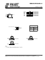
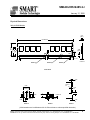
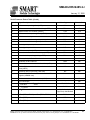
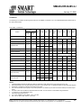
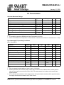
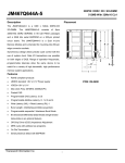
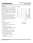
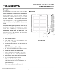
SM646UDR26485-2-I January 31, 2006 Ordering Information Part Numbers Description Device Vendor SM646UDR26485-2-I 64Mx64 (512MB), DDR2, 240-pin DIMM, Unbuffered, Non-ECC, 64Mx8 Based, PC2-5300, DDR2-667-555, 30.00mm, 22Ω DQ termination. Infineon, Rev. A HYB18T512800AF-3S Corporate Headquarters: P. O. Box 1757, Fremont, CA 94538, USA • Tel:(510) 623-1231 • Fax:(510) 623-1434 • E-mail: [email protected] Europe: 5 Kelvin Park South, Kelvin South, East Kilbride, G75 ORH, United Kingdom • Tel: +44-870-870-8747 • Fax: +44-870-870-8757 Asia/Pacific: Plot 18, Lrg Jelawat 4, Kawasan Perindustrian Seberang Jaya 13700, Prai, Penang, Malaysia • Tel: +604-3992909 • Fax: +604-3992903 1 SM646UDR26485-2-I January 31, 2006 Revision History • January 31, 2006 Corrected the OCD Program in the EMRS on page 14. • October 4, 2005 Datasheet released. Corporate Headquarters: P. O. Box 1757, Fremont, CA 94538, USA • Tel:(510) 623-1231 • Fax:(510) 623-1434 • E-mail: [email protected] Europe: 5 Kelvin Park South, Kelvin South, East Kilbride, G75 ORH, United Kingdom • Tel: +44-870-870-8747 • Fax: +44-870-870-8757 Asia/Pacific: Plot 18, Lrg Jelawat 4, Kawasan Perindustrian Seberang Jaya 13700, Prai, Penang, Malaysia • Tel: +604-3992909 • Fax: +604-3992903 2 SM646UDR26485-2-I January 31, 2006 512MByte (64Mx64) DDR2 SDRAM Module - 64Mx8 Based 240-pin DIMM, Unbuffered, Non-ECC Features • • • • • • • • Standard Configuration Cycle Time CAS# Latency Posted CAS#/Additive Latency (AL) Write Latency (WL) Burst Length Burst Type : : : : JEDEC ECC 3.0ns 3.0, 4.0, 5.0 : : : : 0, 1.0, 2.0, 3.0 & 4.0 Read (CAS#) Latency - 1 4, 8 Sequential/Interleave • • • • • • • • No. of Internal Banks per SDRAM : 4 Operating Voltage : 1.8V Refresh : 8K/64ms Device Physicals : FBGA Lead Finish : Gold Length x Height : 133.35mm x 30.00mm No. of sides : Single-sided Mating Connector (Examples) Vertical : Molex - 87705-0021 240-Pin DDR2 DIMM Pin List Pin Pin No. Name Pin Pin No. Name Pin Pin No. Name Pin Pin No. Name Pin Pin No. Name Pin Pin No. Name Pin Pin No. Name Pin Pin No. Name 1 V REF 31 DQ19 61 A4 91 VSS 121 VSS 151 VSS 181 VDDQ 211 DM5 2 V SS 32 VSS 62 VDDQ 92 DQS5# 122 DQ4 152 DQ28 182 A3 212 NC 3 DQ0 33 DQ24 63 A2 93 DQS5 123 DQ5 153 DQ29 183 A1 213 V SS 4 DQ1 34 DQ25 64 VDD 94 VSS 124 VSS 154 VSS 184 VDD 214 DQ46 5 V SS 35 VSS 65 VSS 95 DQ42 125 DM0 155 DM3 185 CK0 215 DQ47 6 DQS0# 36 DQS3# 66 VSS 96 DQ43 126 NC 156 NC 186 CK0# 216 V SS 7 DQS0 37 DQS3 67 VDD 97 VSS 127 VSS 157 VSS 187 VDD 217 DQ52 8 V SS 38 VSS 68 NC 98 DQ48 128 DQ6 158 DQ30 188 A0 218 DQ53 9 DQ2 39 DQ26 69 VDD 99 DQ49 129 DQ7 159 DQ31 189 VDD 219 V SS 10 DQ3 40 DQ27 70 A10/AP 100 VSS 130 VSS 160 VSS 190 BA1 220 CK2 11 V SS 41 VSS 71 BA0 101 SA2 131 DQ12 161 NC 191 VDDQ 221 CK2# 12 DQ8 42 NC 72 VDDQ 102 NC 132 DQ13 162 NC 192 RAS# 222 V SS 13 DQ9 43 NC 73 WE# 103 VSS 133 VSS 163 VSS 193 CS0# 223 DM6 14 V SS 44 VSS 74 CAS# 104 DQS6# 134 DM1 164 NC 194 VDDQ 224 NC 15 DQS1# 45 NC 75 VDDQ 105 DQS6 135 NC 165 NC 195 ODT0 225 V SS 16 DQS1 46 NC 76 CS1# (NC) 106 VSS 136 VSS 166 VSS 196 A13 226 DQ54 17 V SS 47 VSS 77 ODT1 (NC) 107 DQ50 137 CK1 167 NC 197 VDD 227 DQ55 18 NC 48 NC 78 VDDQ 108 DQ51 138 CK1# 168 NC 198 VSS 228 V SS 19 NC 49 NC 79 VSS 109 VSS 139 VSS 169 VSS 199 DQ36 229 DQ60 20 V SS 50 VSS 80 DQ32 110 DQ56 140 DQ14 170 VDDQ 200 DQ37 230 DQ61 ( All specifications of this module are subject to change without notice.) Corporate Headquarters: P. O. Box 1757, Fremont, CA 94538, USA • Tel:(510) 623-1231 • Fax:(510) 623-1434 • E-mail: [email protected] Europe: 5 Kelvin Park South, Kelvin South, East Kilbride, G75 ORH, United Kingdom • Tel: +44-870-870-8747 • Fax: +44-870-870-8757 Asia/Pacific: Plot 18, Lrg Jelawat 4, Kawasan Perindustrian Seberang Jaya 13700, Prai, Penang, Malaysia • Tel: +604-3992909 • Fax: +604-3992903 3 SM646UDR26485-2-I January 31, 2006 240-pin DDR2 DIMM Pin List (Contd.) Pin Pin No. Name Pin Pin No. Name Pin Pin No. Name Pin Pin No. Name Pin Pin No. Name Pin Pin No. Name Pin Pin No. Name 21 DQ10 51 VDDQ 81 DQ33 111 DQ57 141 DQ15 171 CKE1 (NC) 201 VSS Pin Pin No. Name 231 V SS 22 DQ11 52 CKE0 82 VSS 112 VSS 142 VSS 172 VDD 202 DM4 232 DM7 23 V SS 53 VDD 83 DQS4# 113 DQS7# 143 DQ20 173 A15(NC) 203 NC 233 NC 24 DQ16 54 BA2 (NC) 84 DQS4 114 DQS7 144 DQ21 174 A14(NC) 204 VSS 234 V SS 25 DQ17 55 NC 85 VSS 115 VSS 145 VSS 175 VDDQ 205 DQ38 235 DQ62 26 V SS 56 VDDQ 86 DQ34 116 DQ58 146 DM2 176 A12 206 DQ39 236 DQ63 27 DQS2# 57 A11 87 DQ35 117 DQ59 147 NC 177 A9 207 VSS 237 V SS 28 DQS2 58 A7 88 VSS 118 VSS 148 VSS 178 VDD 208 DQ44 238 V DDSPD 29 V SS 59 VDD 89 DQ40 119 SDA 149 DQ22 179 A8 209 DQ45 239 SA0 30 DQ18 60 A5 90 DQ41 120 SCL 150 DQ23 180 A6 210 VSS 240 SA1 Pin Description Table Symbol Type Polarity Function CK0~CK2 SSTL_18 Positive Edge Positive line of the differential pair of system clock inputs. (All DDR2 SDRAM address and control inputs are sampled on the rising edge of their associated clocks. Output data is referenced at the crossings of the clocks.) CK0#~CK2# SSTL_18 Negative Edge Negative line of the differential pair of system clock inputs. ODT0 SSTL_18 Active High On-Die Termination: ODT when high enables termination resistance internal to the DDR2 SDRAM. When enabled, ODT is only applied to each of the following pins: DQ, DQS, and DM. The ODT input will be ignored if disabled in Extended Mode Register (EMRS). CKE0 SSTL_18 Active High Activates the DDR2 SDRAM CLK signal when high and deactivates the CLK signal when low. By deactivating the clocks, CKE low initiates the Power Down mode, or the Self Refresh mode. CS0# SSTL_18 Active Low Enables the associated DDR2 SDRAM command decoder when low and disables decoder when high. When decoder is disabled, new commands are ignored but previous operations continue. RAS#, CAS#, WE# SSTL_18 Active Low When sampled at the positive rising edge of the clock, CAS#, RAS#, and WE# define the operations to be executed by the SDRAM. BA0, BA1 SSTL_18 - Bank Address define to which bank an Activate, Read, Write or Precharge command is being applied. Bank address also determines if the Mode Register or Extended Mode Register is to be accessed during a MRS or EMRS cycle. Corporate Headquarters: P. O. Box 1757, Fremont, CA 94538, USA • Tel:(510) 623-1231 • Fax:(510) 623-1434 • E-mail: [email protected] Europe: 5 Kelvin Park South, Kelvin South, East Kilbride, G75 ORH, United Kingdom • Tel: +44-870-870-8747 • Fax: +44-870-870-8757 Asia/Pacific: Plot 18, Lrg Jelawat 4, Kawasan Perindustrian Seberang Jaya 13700, Prai, Penang, Malaysia • Tel: +604-3992909 • Fax: +604-3992903 4 SM646UDR26485-2-I January 31, 2006 Pin Description Table (Contd.) Symbol Type Polarity Function A0~A9, A10/AP, A11~A13 SSTL_18 - During a Bank Activate command cycle, A0-A13 defines the row address (RA0-RA13) when sampled at the rising clock edge. During a Read or Write command cycle, A0-A9 defines the column address (CA0-CA9) when sampled at the rising clock edge. In addition to the column address, A10/AP is used to invoke autoprecharge operation at the end of the burst read or write cycle. If AP is high, autoprecharge is selected and BA0, BA1 defines the bank to be precharged. If AP is low, autoprecharge is disabled. During a Precharge command cycle, A10/AP is used in conjunction with BA0, BA1 to control which bank(s) to precharge. If AP is high, all banks will be precharged regardless of the state of BA0 or BA1. If AP is low, BA0 and BA1 are used to define which bank to precharge. The address inputs also provide the op-code during Mode Register Set commands. DQ0~DQ63 SSTL_18 - Data Input/Output pins. DQS0~DQS7 SSTL_18 Positive Edge SDRAM differential data strobe for input and output data. DQS0#~DQS7# SSTL_18 Negative Edge SDRAM differential data strobe for input and output data. DM0~DM7 SSTL_18 Active High DM is an input mask signal for write data. Input data is masked when DM is sampled high coincident with that input data during a write access. DM is sampled on both edges of DQS. Although DM pins are input only, the DM loading matches the DQ/DQS loading. SA0~SA2 LVTTL - Slave Address Select for EEPROM. These pins are used to configure the presence-detect device. SDA LVTTL - Serial Bus Data Line for EEPROM. SDA is a bidirectional pin used to transfer addresses and data into and out of the presence-detect portion of the module. A resistor must be connected from the SDA bus line to VDD to act as pull up on the system board. SCL LVTTL - Serial Bus Clock for EEPROM. SCL is used to synchronize the presence-detect data transfer to and from the module. A resistor may be connected from the SCL bus line to VDD to act as pull up on the system board. VDD Supply - SDRAM positive power supply. 1.8V±0.1V VSS Supply - Power supply return (ground). VREF Supply - SDRAM I/O reference supply. VDDQ Supply - SDRAM I/O Driver positive power supply. 1.8V±0.1V VDDSPD Supply - Serial EEPROM positive power supply (wired to a separate power pin at the connector which supports operation from 1.7V to 3.6V). NC - - No Connect DU - - Do not use Corporate Headquarters: P. O. Box 1757, Fremont, CA 94538, USA • Tel:(510) 623-1231 • Fax:(510) 623-1434 • E-mail: [email protected] Europe: 5 Kelvin Park South, Kelvin South, East Kilbride, G75 ORH, United Kingdom • Tel: +44-870-870-8747 • Fax: +44-870-870-8757 Asia/Pacific: Plot 18, Lrg Jelawat 4, Kawasan Perindustrian Seberang Jaya 13700, Prai, Penang, Malaysia • Tel: +604-3992909 • Fax: +604-3992903 5 SM646UDR26485-2-I January 31, 2006 Block Diagram CS0# CKE0 ODT0 DQS0 DQS0# DM0 DQ0 DQ1 DQ2 DQ3 DQ4 DQ5 DQ6 DQ7 S# CKE ODT DQS DQS# DM I/O 0 I/O 1 D0 I/O 2 I/O 3 I/O 4 I/O 5 I/O 6 I/O 7 DQS4 DQS4# DM4 DQ32 DQ33 DQ34 DQ35 DQ36 DQ37 DQ38 DQ39 S# CKE ODT DQS DQS# DM I/O 0 I/O 1 D4 I/O 2 I/O 3 I/O 4 I/O 5 I/O 6 I/O 7 DQS1 DQS1# DM1 DQ8 DQ9 DQ10 DQ11 DQ12 DQ13 DQ14 DQ15 S# CKE ODT DQS DQS# DM I/O 0 I/O 1 D1 I/O 2 I/O 3 I/O 4 I/O 5 I/O 6 I/O 7 DQS5 DQS5# DM5 DQ40 DQ41 DQ42 DQ43 DQ44 DQ45 DQ46 DQ47 S# CKE ODT DQS DQS# DM I/O 0 I/O 1 D5 I/O 2 I/O 3 I/O 4 I/O 5 I/O 6 I/O 7 DQS2 DQS2# DM2 DQ16 DQ17 DQ18 DQ19 DQ20 DQ21 DQ22 DQ23 S# CKE ODT DQS DQS# DM I/O 0 I/O 1 D2 I/O 2 I/O 3 I/O 4 I/O 5 I/O 6 I/O 7 DQS6 DQS6# DM6 DQ48 DQ49 DQ50 DQ51 DQ52 DQ53 DQ54 DQ55 S# CKE ODT DQS DQS# DM I/O 0 I/O 1 D6 I/O 2 I/O 3 I/O 4 I/O 5 I/O 6 I/O 7 DQS3 DQS3# DM3 DQ24 DQ25 DQ26 DQ27 DQ28 DQ29 DQ30 DQ31 S# CKE ODT DQS DQS# DM I/O 0 I/O 1 D3 I/O 2 I/O 3 I/O 4 I/O 5 I/O 6 I/O 7 DQS7 DQS7# DM7 DQ56 DQ57 DQ58 DQ59 DQ60 DQ61 DQ62 DQ63 S# CKE ODT DQS DQS# DM I/O 0 I/O 1 D7 I/O 2 I/O 3 I/O 4 I/O 5 I/O 6 I/O 7 Note: Unless otherwise noted, data resistor values are 22Ω ± 5%. Corporate Headquarters: P. O. Box 1757, Fremont, CA 94538, USA • Tel:(510) 623-1231 • Fax:(510) 623-1434 • E-mail: [email protected] Europe: 5 Kelvin Park South, Kelvin South, East Kilbride, G75 ORH, United Kingdom • Tel: +44-870-870-8747 • Fax: +44-870-870-8757 Asia/Pacific: Plot 18, Lrg Jelawat 4, Kawasan Perindustrian Seberang Jaya 13700, Prai, Penang, Malaysia • Tel: +604-3992909 • Fax: +604-3992903 6 SM646UDR26485-2-I January 31, 2006 5.1Ω SA0 SA1 SA2 SCL SDA SPD EEPROM SA0 V DD SA1 SA2 SCL SDA WP A0~A13 BA0, BA1 RAS# CAS# WE# ODT0 CKE0 CS0# VDDSPD to all SDRAMs (D0~D7) to all SDRAMs (D0~D7) to all SDRAMs (D0~D7) to all SDRAMs (D0~D7) to all SDRAMs (D0~D7) to all SDRAMs (D0~D7) to all SDRAMs (D0~D7) to all SDRAMs (D0~D7) Clock Wiring VDD/V DDQ/VDDSPD/VREF Decoupling Capacitors V SS CK0/CK0# 2 SDRAMs CK1/CK1# 3 SDRAMs CK2/CK2# 3 SDRAMs 2pF 1pF 200Ω 200Ω CK0 CK0# DDR2 SDRAMs CK2 CK2# DDR2 SDRAMs 1pF 200Ω CK1 CK1# DDR2 SDRAMs Notes: 1. Ax, BAx, RAS#, CAS#, WE# resistors: 5.1Ω±5%. Corporate Headquarters: P. O. Box 1757, Fremont, CA 94538, USA • Tel:(510) 623-1231 • Fax:(510) 623-1434 • E-mail: [email protected] Europe: 5 Kelvin Park South, Kelvin South, East Kilbride, G75 ORH, United Kingdom • Tel: +44-870-870-8747 • Fax: +44-870-870-8757 Asia/Pacific: Plot 18, Lrg Jelawat 4, Kawasan Perindustrian Seberang Jaya 13700, Prai, Penang, Malaysia • Tel: +604-3992909 • Fax: +604-3992903 7 SM646UDR26485-2-I January 31, 2006 Physical Dimensions 240-pin DIMM Module 2.57 (max.) 64 1 65 120 55.00 63.00 5.175 10.00 4.00 (min.) 19.80 17.80 30.00 133.35±0.15 5.175 1.27±0.10 Detail A Detail B Detail C Front View 3.00 4x FULL R 4x 5.00 4.00 4x FULL R 65 64 3.80 1.50±0.10 2.50 Detail A 0.20±0.15 2.50±0.20 1.00 0.80±0.05 Detail B 1.00 4x Detail C ( All dimensions are in millimeters with ±0.15mm tolerance unless specified otherwise.) Corporate Headquarters: P. O. Box 1757, Fremont, CA 94538, USA • Tel:(510) 623-1231 • Fax:(510) 623-1434 • E-mail: [email protected] Europe: 5 Kelvin Park South, Kelvin South, East Kilbride, G75 ORH, United Kingdom • Tel: +44-870-870-8747 • Fax: +44-870-870-8757 Asia/Pacific: Plot 18, Lrg Jelawat 4, Kawasan Perindustrian Seberang Jaya 13700, Prai, Penang, Malaysia • Tel: +604-3992909 • Fax: +604-3992903 8 SM646UDR26485-2-I January 31, 2006 Serial Presence Detect Table Byte No. Byte Description Value Supported Value in Hex 0 # of bytes written into serial memory at module manufacturer 128 Bytes 80h 1 Total # of bytes of SPD memory device 256 Bytes 08h 2 Fundamental memory type SDRAM DDR2 08h 3 # of row address on this assembly 14 0Eh 4 # of column address on this assembly 10 0Ah 5 # of Ranks, Package and Height 1, Planar, 30.00mm 60h 6 Data width of this assembly 64 40h 7 Reserved - 00h 8 Voltage interface standard of this assembly SSTL_18 05h 9 SDRAM cycle time from clock @ CAS latency of 5.0 3.0ns 30h 10 SDRAM access time from clock @ CAS latency of 5.0 0.45ns 45h 11 DIMM configuration type Non-ECC 00h 12 Refresh rate & type SR, 7.8 82h 13 Primary SDRAM width 8 08h 14 Error checking SDRAM width - 00h 15 Reserved - 00h 16 SDRAM device attributes : Burst lengths supported 4, 8 0Ch 17 SDRAM device attributes : # of banks on SDRAM device 4 04h 18 SDRAM device attributes : CAS latency 3.0, 4.0, 5.0 38h 19 DIMM Mechanical Characteristics 2.70mm 01h 20 DIMM type information UDIMM 02h 21 SDRAM module attributes None 00h 22 SDRAM device attributes : General Weak Driver, 50Ω ODT 03h 23 SDRAM cycle time from clock @ CAS latency of 4.0 3.75ns 3Dh 24 SDRAM access time from clock @ CAS latency of 4.0 0.50ns 50h 25 SDRAM cycle time from clock @ CAS latency of 3.0 5.0ns 50h 26 SDRAM access time from clock @ CAS latency of 3.0 0.60ns 60h Corporate Headquarters: P. O. Box 1757, Fremont, CA 94538, USA • Tel:(510) 623-1231 • Fax:(510) 623-1434 • E-mail: [email protected] Europe: 5 Kelvin Park South, Kelvin South, East Kilbride, G75 ORH, United Kingdom • Tel: +44-870-870-8747 • Fax: +44-870-870-8757 Asia/Pacific: Plot 18, Lrg Jelawat 4, Kawasan Perindustrian Seberang Jaya 13700, Prai, Penang, Malaysia • Tel: +604-3992909 • Fax: +604-3992903 9 SM646UDR26485-2-I January 31, 2006 Serial Presence Detect Table (Contd.) Byte No. Byte Description Value Supported Value in Hex 27 Minimum row precharge time (=tRP) 15ns 3Ch 28 Minimum row active to row active delay (=tRRD) 7.5ns 1Eh 29 Minimum RAS to CAS delay (=tRCD) 15ns 3Ch 30 Minimum activate precharge time (=tRAS) 45ns 2Dh 31 Module row density 512MB 80h 32 Command and Address signal input setup time 0.20ns 20h 33 Command and Address signal input hold time 0.27ns 27h 34 Data signal input setup time 0.10ns 10h 35 Data signal input hold time 0.17ns 17h 36 Write recovery time (=tWR) 15ns 3Ch 37 Internal write to read command delay (=tWTR) 7.5ns 1Eh 38 Internal read to precharge delay (=tRTP) 7.5ns 1Eh 39 Memory Analysis Probe Characteristics - 00h 40 Extension of tRC and tRFC None 00h 41 Device Minimum activate/auto-refresh time (=tRC) 60ns 3Ch 42 Device Minimum auto-refresh to active/auto-refresh time (=tRFC) 105ns 69h 43 Maximum device cycle time (=tCK max) 8ns 80h 44 Device DQS-DQ skew for DQS and associated DQ signals (=tDQSQ max) 0.24ns 18h 45 Device read data hold skew factor (=tQHS) 0.34ns 22h 46 PLL relock time - 00h 47 TCASE.MAX Delta / ∆T4R4W Delta 95°C, 1.2°C 53h 48 PsiT-A DRAM 60°C/W 78h 49 ∆T0 DT0 5.4°C, 2x refresh, High Temp. Self-Refresh 4Bh 50 ∆T2N (DT2N, UDIMM) or ∆T2Q (DT2Q, RDIMM) 5.7°C 39h 51 ∆T2P (DT2P) 0.57°C 26h 52 ∆T3N (DT3N) 5.7°C 26h Corporate Headquarters: P. O. Box 1757, Fremont, CA 94538, USA • Tel:(510) 623-1231 • Fax:(510) 623-1434 • E-mail: [email protected] Europe: 5 Kelvin Park South, Kelvin South, East Kilbride, G75 ORH, United Kingdom • Tel: +44-870-870-8747 • Fax: +44-870-870-8757 Asia/Pacific: Plot 18, Lrg Jelawat 4, Kawasan Perindustrian Seberang Jaya 13700, Prai, Penang, Malaysia • Tel: +604-3992909 • Fax: +604-3992903 10 SM646UDR26485-2-I January 31, 2006 Serial Presence Detect Table (Contd.) Byte No. Byte Description Value Supported Value in Hex 53 ∆T3P.fast (DT3P fast) 2.15°C 2Bh 54 ∆T3P.slow (DT3P slow) 0.675°C 1Bh 55 ∆T4R (DT4R) / ∆T4R4W S Sign (DT4R4W) 14.8°C, DT4W > DT4R 4Ah 56 ∆T5B (DT5B) 16°C 20h 57 ∆T7 (DT7) 17°C 22h 58 Psi(ca) PLL Not Supported 00h 59 Psi(ca) RED Not Supported 00h 60 ∆TPLL (DTPLL) Not Supported 00h 61 ∆TREG (DTREG) / Toggle Rate Not Supported 00h 62 SPD data revision code 1.2 12h 63 Checksum for bytes 0~62 64 Manufacturer JEDEC ID code 65~71 DEh Infineon’s ID C1h ..........Manufacturer JEDEC ID code Not Used 00h 72 Manufacturing location Location xxh 73~90 Manufacturer part # HYS64T64000HU-3S-A P. No 91 Manufacturer revision code Rev 2.x 2xh 92 ........Manufacturer revision code None xxh 93 Manufacturing data (Year) Date Date 94 Manufacturing data (Week) Date Date 95~98 Assembly serial # Serial Number S. No 99~127 Unused storage locations - 00h Corporate Headquarters: P. O. Box 1757, Fremont, CA 94538, USA • Tel:(510) 623-1231 • Fax:(510) 623-1434 • E-mail: [email protected] Europe: 5 Kelvin Park South, Kelvin South, East Kilbride, G75 ORH, United Kingdom • Tel: +44-870-870-8747 • Fax: +44-870-870-8757 Asia/Pacific: Plot 18, Lrg Jelawat 4, Kawasan Perindustrian Seberang Jaya 13700, Prai, Penang, Malaysia • Tel: +604-3992909 • Fax: +604-3992903 11 SM646UDR26485-2-I January 31, 2006 Mode Register Table Definition The mode register stores the data for controlling the various operating modes of DDR2 SDRAM. It controls CAS latency, burst length, burst sequence, test mode, DLL reset, tWR and various vendor specific options to make DDR2 SDRAM useful for various applications. The default value of the mode register is not defined, therefore the mode register must be written after powerup for proper operation. The mode register is written by asserting low on CS#, RAS#, CAS#, WE#, BA0 and BA1, while controlling the state of address pins A0~A15. The DDR2 SDRAM should be in all bank precharge with CKE already high prior to writing into the mode register. The mode register set command cycle time (tMRD) is required to complete the write operation to the mode register. The mode register contents can be changed using the same command and clock cycle requirements during normal operation as long as all banks are in the precharge state. The mode register is divided into various fields depending on functionality. Burst length is defined by A0~A2 with options of 4 and 8 bit burst lengths. The burst length decodes are compatible with DDR SDRAM. Burst address sequence type is defined by A3, CAS latency is defined by A4~A6. The DDR2 doesn’t support half clock latency mode. A7 is used for test mode. A8 is used for DLL reset. A7 must be set to low for normal MRS operation. Write recovery time tWR is defined by A9~A11. BA2 BA1 BA0 A15~A14 A13 A12 A11 A10 A9 A8 A7 A6 A5 A4 A3 A2 A1 A0 Address Field M18 M17 M16 M15~M14 M13 M12 M11 M10 M9 M8 M7 M6 M5 M4 M3 M2 M1 M0 Mode Register 01 0 PD DLL TM 01 MR WR CAS Latency BT Burst Length Burst Length M8 M7 Mode No 0 Normal 0 Sequential 1 Yes 1 Test 1 Interleave 1 Slow exit (tXARDS) M10 M9 WR (cycles) 2 0 0 0 Reserved 0 0 1 2 0 1 0 3 MRS mode 0 1 1 4 0 0 MRS 1 0 0 5 0 1 6 0 1 EMRS (1) 1 1 0 EMRS (2): Reserved 1 1 0 Reserved EMRS (3): Reserved 1 1 1 Reserved M2 M1 M0 BL 0 1 0 4 0 1 1 8 CAS Latency DDR2-800 Fast exit (t XARD) M11 DDR2-667 0 Write recovery for autoprecharge DDR2-533 Active power down exit time M16 1 Burst Type 0 M17 1 M3 DDR2-400 M12 DLL Reset M6 M5 M4 Latency 0 0 0 Reserved 0 0 1 Reserved 0 1 0 2.0 (optional) 0 1 1 3.0 1 0 0 4.0 1 0 1 5.0 1 1 0 Reserved 1 1 1 Reserved Notes: 1. BA2 and A14~A15 are reserved for future use and must be programmed to 0 when setting the mode register. 2. WR min is determinedby tCK max and WR max is determined by tCK min. WR in clock cycles is calculated by dividing tWR (in ns) by tCK (in ns) and rounding up to the next integer. The mode register must be programmed to this value. Corporate Headquarters: P. O. Box 1757, Fremont, CA 94538, USA • Tel:(510) 623-1231 • Fax:(510) 623-1434 • E-mail: [email protected] Europe: 5 Kelvin Park South, Kelvin South, East Kilbride, G75 ORH, United Kingdom • Tel: +44-870-870-8747 • Fax: +44-870-870-8757 Asia/Pacific: Plot 18, Lrg Jelawat 4, Kawasan Perindustrian Seberang Jaya 13700, Prai, Penang, Malaysia • Tel: +604-3992909 • Fax: +604-3992903 12 SM646UDR26485-2-I January 31, 2006 Extended Mode Register Table Definition The extended mode register controls functions beyond those controlled by the mode register; these additional functions are DLL enable/ disable, output drive strength, ODT (RTT), Posted CAS additive latency (AL), off-chip driver impedance calibration (OCD), DQS# enable/disable, RDQS/RDQS# enable/disable, and OUTPUT enable/disable. The extended mode register is programmed via the LOAD MODE (LM) command and will retain the stored information until it is programmed again or the device loses power. Reprogramming the extended mode register will not alter the contents of the memory array, provided it is performed correctly. The extended mode register must be loaded when all banks are idle and no bursts are in progress, and the controller must wait the specified time tMRD before initiating any subsequent operation. Violating either of these requirements could result in unspecified operation. Notes: 1. BA2 and A14~A15 are reserved for future use and must be programmed to 0 when setting the mode register. 2. When the adjust mode of the OCD Calibration Program is issued, AL from previously set value must be applied. 3. After setting the OCD Calibration Program to default, OCD mode needs to be exited by setting A9-A7 to 000. 4. Outputs disabled - DQs, DQSs, DQS#s, RDQSs, RDQS#s. This feature is used in conjunction with DIMM I DD measurements when I DDQ is not desired to be included. 5. If RDQS is enabled, the DM function is disabled. RDQS is active for reads and don’t care for writes. Corporate Headquarters: P. O. Box 1757, Fremont, CA 94538, USA • Tel:(510) 623-1231 • Fax:(510) 623-1434 • E-mail: [email protected] Europe: 5 Kelvin Park South, Kelvin South, East Kilbride, G75 ORH, United Kingdom • Tel: +44-870-870-8747 • Fax: +44-870-870-8757 Asia/Pacific: Plot 18, Lrg Jelawat 4, Kawasan Perindustrian Seberang Jaya 13700, Prai, Penang, Malaysia • Tel: +604-3992909 • Fax: +604-3992903 13 SM646UDR26485-2-I January 31, 2006 Extended Mode Register Table BA2 BA1 BA0 A15~A14 A13 A12 A11 A10 A9 A8 A7 A6 A5 A4 A3 A2 A1 A0 Address Field E18 E17 E16 E15~E14 E13 E12 E11 E10 E9 E8 E7 E6 E5 E4 E3 E2 E1 E0 Extended Mode Register 01 0 Qoff RDQS DQS# RTT D.I.C DLL 01 EMR RTT Additive latency E6 E2 RTT (Nominal) MRS 0 0 ODT Disabled 1 EMRS (1) 0 1 75 ohm 0 Enable 1 0 EMRS (2) 1 0 150 ohm 1 Disable 1 1 EMRS (3): Reserved 1 1 50 ohm E17 E16 0 0 0 MRS mode E3 Additive Latency OCD calibration mode exit; maintain setting 0 0 0 0 1 Drive (1) 0 0 1 1 1 0 Drive (0) 0 1 0 2 0 1 1 Adjust mode 2 (See page 13) 0 1 1 3 1 1 1 OCD calibration default3 (See page 13) 1 0 0 4 1 0 1 Reserved 1 1 0 Reserved 1 1 1 Reserved E7 0 0 0 0 0 0 Output buffer enabled 1 Output buffer disabled DQS# 0 Enable 1 Disable DLL Enable E4 E8 0 E10 E0 E5 E9 OCD Calibration Program Qoff (Optional) 4 (See page 13) E12 OCD Program E1 Output Driver Impedence Control Driver Size 0 Normal 100% 1 Weak 60% E11 (RDQS Enable) E10 (DQS# Enable) 0 (Disable) Strobe Function Matrix RDQS/DM RDQS# DQS DQS# 0 (Enable) DM Hi-z DQS DQS# E11 RDQS 0 (Disable) 1 (Disable) DM Hi-z DQS Hi-z 0 Disable 1 (Enable) 0 (Enable) RDQS RDQS# DQS DQS# 1 Enable 5 (See page 13) 1 (Enable) 1 (Disable) RDQS Hi-z DQS Hi-z Corporate Headquarters: P. O. Box 1757, Fremont, CA 94538, USA • Tel:(510) 623-1231 • Fax:(510) 623-1434 • E-mail: [email protected] Europe: 5 Kelvin Park South, Kelvin South, East Kilbride, G75 ORH, United Kingdom • Tel: +44-870-870-8747 • Fax: +44-870-870-8757 Asia/Pacific: Plot 18, Lrg Jelawat 4, Kawasan Perindustrian Seberang Jaya 13700, Prai, Penang, Malaysia • Tel: +604-3992909 • Fax: +604-3992903 14 SM646UDR26485-2-I January 31, 2006 Commands The following Truth Tables provide a general reference of available commands. For a more detailed description please refer to the device data sheets. Truth Table - Commands CKE Function BA0~ An8~A11 CS# RAS# CAS# WE# H L L L L BA H H L L L H X X X X 1 Self Refresh Entry H L L L L H X X X X 1 H X X X Self Refresh Exit L H X X X X 1, 7 L H H H Previous cycle Current cycle (Extended) Mode Register Set H Refresh BAn9 A10 A9~A0 OP Code Notes 1, 2 Single Bank Precharge H H L L H L BA X L X 1, 2 Precharge All Banks H H L L H L X X H X 1 Bank Activate H H L L H H BA Write H H L H L L BA Column L Column 1, 2, 3 Write with Auto-Precharge H H L H L L BA Column H Column 1, 2, 3 Read H H L H L H BA Column L Column 1, 2, 3 Read with Auto-Precharge H H L H L H BA Column H Column 1, 2, 3 No Operation H X L H H H X X X X 1 Device Deselect H X H X X X X X X X 1 H X X X Power Down Entry H L X X X X 1, 4 L H H H H X X X X X X X 1, 4 L H H H Power Down Exit L H Row Address 1, 2 Notes: 1. 2. 3. 4. 5. 6. 7. 8. 9. All DDR2 SDRAM commands are defined by states of CS#, RAS#, CAS#, WE# and CKE at the rising edge of the clock. Bank addresses BA0, BA1, BA2 (BA) determine which bank is to be operated upon. For (E)MRS BA selects an (Extended) Mode Register. Burst reads or writes at BL=4 cannot be terminated or interrupted. The Power Down Mode does not perform any refresh operations. The duration of power down is therefore limited by the refresh requirements. The state of ODT does not affect the states described in this table. The ODT function is not available during Self Refresh. “X” means “H or L (but a defined logic level)”. Self Refresh Exit is asynchronous. An = A12 for 256Mb, A13 for 512Mb & 1 Gb, A14 for 2Gb. BAn = BA1 for upto 512Mb , BA2 for 1 Gb & 2Gb. Corporate Headquarters: P. O. Box 1757, Fremont, CA 94538, USA • Tel:(510) 623-1231 • Fax:(510) 623-1434 • E-mail: [email protected] Europe: 5 Kelvin Park South, Kelvin South, East Kilbride, G75 ORH, United Kingdom • Tel: +44-870-870-8747 • Fax: +44-870-870-8757 Asia/Pacific: Plot 18, Lrg Jelawat 4, Kawasan Perindustrian Seberang Jaya 13700, Prai, Penang, Malaysia • Tel: +604-3992909 • Fax: +604-3992903 15 SM646UDR26485-2-I January 31, 2006 DC Characteristics Absolute Maximum Ratings Parameter Symbol Ratings Unit VDD -1.0 ~ 2.3 V Voltage on VDDQ relative to VSS VDDQ -0.5 ~ 2.3 V Voltage on any pin relative to VSS VIN, VOUT -0.5 ~ 2.3 V Voltage on VDDSPD relative to VSS VDDSPD 1.7 ~ 3.6 V Operating Temperature (Ambient) TOPR 0 to +65 °C Operating Temperature (Case) TCASE 0 to +95 °C TSTG -55 to +100 °C Voltage on VDD relative to VSS Storage Temperature Notes 1, 2 Notes: 1. It is possible to operate the DRAM above Case Temperature up to 95ºC. 2. Above 85°C DRAM Case Temperature the Auto-Refresh command interval has to be reduced to tREFI = 3.9µs Recommended DC Operating Conditions (TA = 0 to +65°C) Parameter Symbol Min Typ Max Unit VDD 1.7 1.8 1.9 V I/O Supply Voltage VDDQ 1.7 1.8 1.9 V I/O Reference Voltage VREF 0.49*VDDQ 0.50*VDDQ 0.51*VDDQ mV I/O Termination Voltage VTT VREF - 0.04 VREF VREF + 0.04 V SPD Voltage VDDSPD 1.7 - 3.6 V Input High Voltage VIH(DC) VREF + 0.125 - VDDQ + 0.3 V Input Low Voltage VIL(DC) -0.3 - VREF - 0.125 V Input Voltage Level, CK/CK# VIN(DC) -0.3 - VDDQ + 0.3 V Input Differential Voltage, CK/CK# VID(DC) 0.25 - VDDQ + 0.6 V VSS 0 0 0 V Supply Voltage Ground Notes 1, 2 3 Notes: 1. VREF is expected to track variation in VDDQ. VREF = 0.5 x VDDQ. 2. Peak to peak noise (non-common mode) on VREF may not exceed ±1% of the DC value. Peak to peak AC noise on VREF may not exceed ±2% of VREF (DC). This measurement is to be taken at the nearest VREF bypass capacitor. 3. VTT is not used on the module. It is the voltage used on the system board to terminate all the signals. However, this supply should track the variations in DC level of VREF. Corporate Headquarters: P. O. Box 1757, Fremont, CA 94538, USA • Tel:(510) 623-1231 • Fax:(510) 623-1434 • E-mail: [email protected] Europe: 5 Kelvin Park South, Kelvin South, East Kilbride, G75 ORH, United Kingdom • Tel: +44-870-870-8747 • Fax: +44-870-870-8757 Asia/Pacific: Plot 18, Lrg Jelawat 4, Kawasan Perindustrian Seberang Jaya 13700, Prai, Penang, Malaysia • Tel: +604-3992909 • Fax: +604-3992903 16 SM646UDR26485-2-I January 31, 2006 Capacitance (VDD = 1.8V±0.1V, TCase = +25°C) Parameter Symbol Min Max Unit CCK 3.0 6.0 pF CDCK - 0.75 pF CI 8.0 16.0 pF Input Capacitance delta (all other input-only pins) CDI - 2.0 pF Input/Output Capacitance (DQ, DM, DQS, DQS#) CI0 2.5 3.5 pF CDI0 - 0.5 pF Input Capacitance (CKn, CKn#) Input Capacitance delta (CKn, CKn#) Input Capacitance (all other input-only pins) Input/Output Capacitance delta (DQ, DM, DQS, DQS#) AC Operating Conditions (VDD = 1.8V±0.1V, VSS = 0V) Parameter Symbol Min Max Unit Notes Input High Logic Voltage VIH(AC) VREF + 0.250 - V 1, 2 Input Low Logic Voltage VIL(AC) - VREF - 0.250 V 1, 2 Input differential voltage, CK and CK# inputs VID(AC) 0.5 VDDQ + 0.6 V 1, 2, 3 Input crossing point voltage, CK and CK# inputs VIX(AC) 0.5*VDDQ - 0.175 0.5*VDDQ + 0.175 V 1, 2, 3 AC differential crossing point voltage VOX(AC) 0.5*VDDQ - 0.125 0.5*VDDQ + 0.125 V 3 Notes: 1. Input slew rate is 1V/ns. 2. Inputs are not recognized as valid until VREF stabilizes. 3. VID is the magnitude of the difference between the input level on CK and the input level on CK#. 4. The value of VIX/VOX is expected to equal 0.5*VDDQ of the transmitting device and must track variations in the DC level of the same. Corporate Headquarters: P. O. Box 1757, Fremont, CA 94538, USA • Tel:(510) 623-1231 • Fax:(510) 623-1434 • E-mail: [email protected] Europe: 5 Kelvin Park South, Kelvin South, East Kilbride, G75 ORH, United Kingdom • Tel: +44-870-870-8747 • Fax: +44-870-870-8757 Asia/Pacific: Plot 18, Lrg Jelawat 4, Kawasan Perindustrian Seberang Jaya 13700, Prai, Penang, Malaysia • Tel: +604-3992909 • Fax: +604-3992903 17 SM646UDR26485-2-I January 31, 2006 ODT DC Electrical Characteristics Parameter Symbol Min Nom Max Unit Notes RTT effective impedence value for 75Ω setting EMR (A6, A2) = 0, 1 RTT1(EFF) 60 75 90 Ω 1 RTT effective impedence value for 150Ω setting EMR (A6, A2) = 1, 0 RTT2(EFF) 120 150 180 Ω 1 RTT effective impedence value for 50Ω setting EMR (A6, A2) = 1, 1 RTT3(EFF) 40 50 60 Ω 1 Deviation of VM with respect to VDDQ/2 ∆VM -6 +6 % 2 Notes: 1. RTT1(EFF) and RTT2(EFF) are determined by applying VIH(AC) and VIL(AC) to pin under test separately, then V IH ( AC ) – V IL ( AC ) measure current I(VIH(AC)) and I(VIL(AC)) respectively. R TT ( EFF ) = ------------------------------------------------------------------I (V ) – I (V ) IH ( AC ) IL ( AC ) 2. Measured voltage (VM) at tested pin with no load. 2 × VM ∆VM = -------------------- –1 V DDQ × 100 % Output DC Current Drive Parameter Symbol Min Max Unit Notes Output Minimum Source DC Current IOH -13.4 - mA 1, 3, 4 Output Minimum Sink DC Current IOL 13.4 - mA 2, 3, 4 Notes: 1. For I OH (DC); VDDQ = 1.7V, VOUT = 1420mV. (VOUT - VDDQ)/I OH must be less than 21Ω for values of VOUT between VDDQ and VDDQ - 280mV. 2. For I OL (DC); VDDQ = 1.7V, VOUT = 280mV. VOUT/I OL must be less than 21Ω for values of VOUT between 0V and 280mV. 3. The DC value of VREF applied to the receiving device is set to VTT. 4. The values of I OH (DC) and I OL (DC) are based on the conditions given in Notes 1 and 2. They are used to test device drive current capability to ensure VIH min plus a noise margin and VIL max minus a noise margin are delivered to an SSTL_18 receiver. The actual current values are derived by shifting the desired driver operating point along a 21Ω load line to define a convenient driver current for measurement. Corporate Headquarters: P. O. Box 1757, Fremont, CA 94538, USA • Tel:(510) 623-1231 • Fax:(510) 623-1434 • E-mail: [email protected] Europe: 5 Kelvin Park South, Kelvin South, East Kilbride, G75 ORH, United Kingdom • Tel: +44-870-870-8747 • Fax: +44-870-870-8757 Asia/Pacific: Plot 18, Lrg Jelawat 4, Kawasan Perindustrian Seberang Jaya 13700, Prai, Penang, Malaysia • Tel: +604-3992909 • Fax: +604-3992903 18 SM646UDR26485-2-I January 31, 2006 OCD Default Output Characteristics (VDD = 1.8V±0.1V, VSS = 0V, TA = 0 to +65°C) Parameter Symbol Output Impedance Pull-up and Pull-down mismatch Output Slew Rate SOUT Output Step Size for Calibration Min Nom Max Unit Notes 12.6 18 23.4 Ω 1, 2 0 4 Ω 1, 2, 3 1.5 5 V/ns 0 1.5 Ω 1, 4, 5, 7 6 Notes: 1. Absolute specifications: 0°C ≤ Tcase ≤ +85°C; VDDQ = +1.8V±0.1V, VDD = +1.8V±0.1V. 2. Impedance measurement condition for output source DC current: VDDQ = 1.7V; VOUT = 1420mV; (VOUT VDDQ)/I OH must be less than 23.4Ω for values of VOUT between VDDQ and VDDQ - 280mV. Impedance measurement condition for output sink DC current: VDDQ = 1.7V; VOUT = 280mV; VOUT/I OL must be less than 23.4Ω for values of VOUT between 0V and 280mV. 3. Mismatch is absolute value between pull-up and pull-down, both are measured at same temperature and voltage. 4. Output slew rate for falling and rising edges is measured between VTT - 250mV and VTT + 250mV for single ended signals. For differential signals output slew rate is measured between DQS - DQS# = -500mV and DQS# - DQS = +500mV. Output slew rate is guaranteed by design, but is not necessarily tested on each device. 5. The absolute value of the slew rate as measured from VIL (DC) max to VIH (DC) min is equal to or greater than the slew rate as measured from VIL (AC) max to VIH (AC) min. This is guaranteed by design and characterization. 6. This represents the step size when the OCD is near 18Ω at nominal conditions across all process and represent only the DRAM uncertainty. 7. Timing skew due to DRAM output slew rate mis-match between DQS/DQS# and associated DQs is included in tDQSQ and tQHS specification. Output Slew Rate Load Diagram V TT 25Ω Output (VOUT) Reference Point Corporate Headquarters: P. O. Box 1757, Fremont, CA 94538, USA • Tel:(510) 623-1231 • Fax:(510) 623-1434 • E-mail: [email protected] Europe: 5 Kelvin Park South, Kelvin South, East Kilbride, G75 ORH, United Kingdom • Tel: +44-870-870-8747 • Fax: +44-870-870-8757 Asia/Pacific: Plot 18, Lrg Jelawat 4, Kawasan Perindustrian Seberang Jaya 13700, Prai, Penang, Malaysia • Tel: +604-3992909 • Fax: +604-3992903 19 SM646UDR26485-2-I January 31, 2006 IDD Specification Parameters and Test Conditions (VDD = 1.8V±0.1V, VSS = 0V, TA = 0 to +65°C) 3.0ns CL 5.0 Unit Operating one bank active–precharge current; tCK = tCK(IDD), tRC = tRC(IDD), tRAS = tRASmin(IDD); CKE and CS# are HIGH between valid commands; Address bus inputs are SWITCHING; Data bus inputs are SWITCHING 570 mA IDD1 Operating one bank active–read–precharge current; I OUT = 0mA; BL = 4, CL = CL(IDD), AL = 0; tCK = tCK(IDD), tRC = tRC(IDD), tRAS = tRASmin(IDD), tRCD = tRCD(IDD) ; CKE and CS# are HIGH between valid commands; Address bus inputs are SWITCHING; Data pattern is same as IDD4W 680 mA IDD2P Precharge power–down current; All banks idle; tCK = tCK(IDD); CKE is LOW; Other control and address bus inputs are STABLE; Data bus inputs are FLOATING 40 mA IDD2Q Precharge quiet standby current; All banks idle; tCK = tCK(IDD); CKE is HIGH, CS# is HIGH; Other control and address bus inputs are STABLE; Data bus inputs are FLOATING 320 mA IDD2N Precharge standby current; All banks idle; tCK = tCK(IDD); CKE is HIGH, CS# is HIGH; Other control and address bus inputs are SWITCHING; Data bus inputs are SWITCHING 400 mA IDD3P Active power–down current; All banks open; t CK = tCK(IDD); CKE is LOW; Other control and address bus inputs are STABLE; Data bus inputs are FLOATING Fast PDN Exit MRS(12) = 0 150 mA Slow PDN Exit MRS(12) = 1 50 mA Symbol Parameter IDD0 IDD3N Active standby current; All banks open; tCK = tCK(IDD), tRAS = tRASmax(IDD), tRP = tRP(IDD) ; CKE is HIGH, CS# is HIGH between valid commands; Other control and address bus inputs are SWITCHING; Data bus inputs are SWITCHING 400 mA IDD4W Operating burst write current; All banks open, Continuous burst writes; BL = 4, CL = CL(IDD), AL = 0; tCK = tCK(IDD), tRAS = tRASmax(IDD), tRP = tRP(IDD); CKE is HIGH, CS# is HIGH between valid commands; Address bus inputs are SWITCHING; Data bus inputs are SWITCHING 1120 mA IDD4R Operating burst read current; All banks open, Continuous burst reads, IOUT = 0mA; BL = 4, CL = CL(IDD), AL = 0; tCK = tCK(IDD), tRAS = tRASmax(IDD), tRP = tRP(IDD); CKE is HIGH, CS# is HIGH between valid commands; Address bus inputs are SWITCHING; Data pattern is same as IDD4W 1040 mA IDD5B Burst refresh current; tCK = tCK(IDD); Refresh command at every t RFC(IDD) interval; CKE is HIGH, CS# is HIGH between valid commands; Other control and address bus inputs are SWITCHING; Data bus inputs are SWITCHING 1120 mA IDD6 Self refresh current; CK and CK# at 0V; CKE ≤ 0.2V; Other control and address bus inputs are FLOATING; Data bus inputs are FLOATING 40 mA IDD7 Operating bank interleave read current; All bank interleaving reads, I OUT = 0mA; BL = 4, CL = CL(IDD), AL = tRCD(IDD) -1*tCK(IDD); tCK = tCK(IDD), tRC = tRC(IDD), tRRD = tRRD(IDD), tRCD = 1*tCK(IDD); CKE is HIGH, CS# is HIGH between valid commands; Address bus inputs are STABLE during DESELECTs; Data pattern is same as IDD4R 1180 mA Corporate Headquarters: P. O. Box 1757, Fremont, CA 94538, USA • Tel:(510) 623-1231 • Fax:(510) 623-1434 • E-mail: [email protected] Europe: 5 Kelvin Park South, Kelvin South, East Kilbride, G75 ORH, United Kingdom • Tel: +44-870-870-8747 • Fax: +44-870-870-8757 Asia/Pacific: Plot 18, Lrg Jelawat 4, Kawasan Perindustrian Seberang Jaya 13700, Prai, Penang, Malaysia • Tel: +604-3992909 • Fax: +604-3992903 20 SM646UDR26485-2-I January 31, 2006 IDD Specification Parameters and Test Conditions (Contd.) Notes: 1. IDD specifications are tested after the device is properly initialized. 2. Input slew rate is specified by AC Parametric Test Condition. 3. IDD parameters are specified with ODT disabled. 4. Data bus consists of DQ, DM, DQS, DQS#. IDD values must be met with all combinations of ERMS bits 10 and 11. 5. Definitions for IDD LOW = Vin ≤ VIL(AC)(max) HIGH = Vin ≥ VIH(AC)(min) STABLE = inputs stable at a HIGH or LOW level FLOATING = inputs at VREF = VDDQ/2 SWITCHING = inputs changing between HIGH and LOW every other clock cycle (once per two clocks) for address and control signals, and inputs between HIGH and LOW every other data transfer (once per clock) for DQ signals not including masks of strobes. IDD Testing Parameters DDR2-667 Parameter 5-5-5 Units CL(IDD) 5 tCK tRCD(IDD) 15 ns tRC(IDD) 60 ns tRRD(IDD) 7.5 ns tCK(IDD) 3 ns tRASmin(IDD) 45 ns tRASmax(IDD) 70000 ns tRP(IDD) 15 ns tRFC(IDD) 105 ns Corporate Headquarters: P. O. Box 1757, Fremont, CA 94538, USA • Tel:(510) 623-1231 • Fax:(510) 623-1434 • E-mail: [email protected] Europe: 5 Kelvin Park South, Kelvin South, East Kilbride, G75 ORH, United Kingdom • Tel: +44-870-870-8747 • Fax: +44-870-870-8757 Asia/Pacific: Plot 18, Lrg Jelawat 4, Kawasan Perindustrian Seberang Jaya 13700, Prai, Penang, Malaysia • Tel: +604-3992909 • Fax: +604-3992903 21 SM646UDR26485-2-I January 31, 2006 Device AC Operating Conditions Parameter 3.0ns @ CL 5.0 DDR2-667 Symbol Min Clock cycle time CL=5.0 tCK CL=4.0 CL=3.0 Unit Notes Max 3000 8000 ps 12, 20 3750 8000 ps 12, 20 5000 8000 ps 12, 20 Clock high-level width tCH 0.45 0.55 t CK 14 Clock low-level width tCL 0.45 0.55 t CK 14 Clock half period tHP Min (tCL, tCH) - ps 15 DQ output access time from CK/CK# tAC -450 +450 ps Data-out high-impedence window from CK/CK# tHZ - tAC(max) ps 4, 5 Data-out low-impedence window from CK/CK# tLZ tAC(min) tAC(max) ps 4, 6 DQ & DM input setup time relative to DQS tDS 100 - ps 3, 11, 17 DQ & DM input hold time relative to DQS tDH 175 - ps 3, 11, 17 DQ & DM input pulse width (for each input) tDIPW 0.35 - t CK Data hold skew factor tQHS - 340 ps DQ-DQS hold, DQS to first DQ to go nonvalid, per access tQH tHP - t QHS - ps DQS input high pulse width tDQSH 0.35 - t CK DQS input low pulse width tDQSL 0.35 - t CK DQS output access time from CK/CK# tDQSCK -400 +400 ps DQS falling edge to CK rising - setup time tDSS 0.2 - t CK DQS falling edge from CK rising - hold time tDSH 0.2 - t CK DQS-DQ skew, DQS to last DQ valid, per group, per access tDQSQ - 240 ps 11,13 DQS read preamble tRPRE 0.9 1.1 t CK 18 11,13 DQS read postamble tRPST 0.4 0.6 t CK DQS write preamble setup time tWPRES 0 - ps DQS write preamble tWPRE 0.35 - t CK DQS write postamble tWPST 0.4 0.6 t CK Write command to first DQS latching transition tDQSS WL - 0.25 WL + 0.25 t CK Address & control input pulse width for each input tIPW 0.6 - t CK Address and control input setup time tIS 200 - ps 2, 17 Address and control input hold time tIH 275 - ps 2, 17 CAS# to CAS# command delay tCCD 2 - t CK OCD Drive mode delay tOIT 0 12 ns 8, 9 7 Corporate Headquarters: P. O. Box 1757, Fremont, CA 94538, USA • Tel:(510) 623-1231 • Fax:(510) 623-1434 • E-mail: [email protected] Europe: 5 Kelvin Park South, Kelvin South, East Kilbride, G75 ORH, United Kingdom • Tel: +44-870-870-8747 • Fax: +44-870-870-8757 Asia/Pacific: Plot 18, Lrg Jelawat 4, Kawasan Perindustrian Seberang Jaya 13700, Prai, Penang, Malaysia • Tel: +604-3992909 • Fax: +604-3992903 22 SM646UDR26485-2-I January 31, 2006 Device AC Operating Conditions (Contd.) Parameter 3.0ns @ CL5.0 DDR2-667 Symbol Min Unit Notes 24 Max CKE low to CK,CK# uncertainity tDELAY 3.475 3.475 ns ACTIVE to ACTIVE (same bank) command tRC 60 - ns ACTIVE bank a to ACTIVE bank b command tRRD 7.5 - ns ACTIVE to READ or WRITE delay tRCD 15 - ns ACTIVE to PRECHARGE command tRAS 45 70000 ns 16 Internal READ to precharge command delay tRTP 7.5 - ns 19, 23 Write recovery time tWR 15 - ns 23 Auto precharge write recovery + Precharge time tDAL tWR + tRP - t CK 18 Internal WRITE to READ command delay tWTR 7.5 - ns 23 PRECHARGE command period tRP 15 - ns LOAD MODE command cycle time tMRD 2 - t CK REFRESH to REFRESH command interval tRFC 105 - ns 10 Average periodic refresh Interval tREFI - 7.8 µs 10 Exit self refresh to non-READ command tXSNR tRFC(min) + 10 - ns Exit self refresh to READ command tXSRD 200 - t CK ODT turn-on delay tAOND 2 2 t CK ODT turn-on tAON tAC(min) tAC(max) + 1000 ps ODT turn-off delay tAOFD 2.5 2.5 t CK ODT turn-off tAOF tAC(min) tAC(max) + 600 ps ODT turn-on (power-down mode) tAONPD tAC(min) + 2000 2*tCK + tAC(max) + 1000 ps ODT turn-off (power-down mode) tAOFPD tAC(min) + 2000 2.5*tCK + tAC(max) + 1000 ps ODT to power-down entry latency tANPD 3 ODT power-down exit latency tAXPD 8 Exit active power-down to READ command, MR[bit12=0] tXARD 2 - t CK Exit active power-down to READ command, MR[bit12=1] tXARDS 7 - AL - t CK Exit precharge power down to any non-read command tXP 2 - t CK CKE minimum pulse width (high and low pulse width) tCKE 3 - t CK 23 21 22 t CK t CK Corporate Headquarters: P. O. Box 1757, Fremont, CA 94538, USA • Tel:(510) 623-1231 • Fax:(510) 623-1434 • E-mail: [email protected] Europe: 5 Kelvin Park South, Kelvin South, East Kilbride, G75 ORH, United Kingdom • Tel: +44-870-870-8747 • Fax: +44-870-870-8757 Asia/Pacific: Plot 18, Lrg Jelawat 4, Kawasan Perindustrian Seberang Jaya 13700, Prai, Penang, Malaysia • Tel: +604-3992909 • Fax: +604-3992903 23 SM646UDR26485-2-I January 31, 2006 Notes: 1. 2. 3. 4. 5. 6. 7. 8. 9. 10. 11. 12. 13. 14. 15. 16. 17. 18. 19. 20. 21. 22. 23. 24. The AC and DC input level specifications are as defined in the SSTL_18 standard (i.e., the receiver will effectively switch as a result of the signal crossing the AC input level and will remain in that state as long as the signal does not ring back above [below] the DC input LOW [HIGH] level. Command/Address minimum input slew rate = 1.0V/ns and is referenced to the crosspoint of CK/CK#. tIS timing is referenced to V IH (AC) for a rising signal and VIL (AC) for a fallng signal. t IH timing is referenced to V IH (DC) for a rising signal and VIL (DC) for a fallng signal. Derating values for Command/Address input signal slew rates < 1.0V/ns are TBD. Data minimum input slew rate = 1.0V/ns and is referenced to the crosspoint of DQS/DQS# if differential strobe feature is enabled. t DS timing is referenced to V IH (AC) for a rising signal and VIL (AC) for a fallng signal. t DH timing is referenced to V IH (DC) for a rising signal and VIL (DC) for a fallng signal. Derating values for Data input signal slew rates < 1.0V/ns are TBD. tHZ and tLZ transitions occur in the same access time windows as valid data transitions. These parameters are not referenced to a specific voltage level, but specify when the device output is no longer driving (t HZ ) or begins driving (tLZ). This maximum value is derived from the reference test load. t HZ (MAX) will prevail over a tDQSCK (MAX) + tRPST (MAX) condition. tLZ (MIN) will prevail over a t DQSCK (MIN) + tRPRE (MAX) condition. The intent of the Don’t Care state after completion of the postamble is the DQS driven signal should be high, low or high-Z and that any signal transition within the input switching region must follow valid input requirements. That is if DQS transitions high [above VIH DC (MIN)] then it must not transition low (below VIH DC) prior to tDQSH(min). This is not a device limit. The device will operate with a negative value, but system performance could be degraded due to bus turnaround. It is recommended that DQS be valid (HIGH or LOW) on or before the WRITE command. The case shown (DQS going from High-Z to logic LOW) applies when no WRITEs were previously in progress on the bus. If a previous WRITE was in progress, DQS could be HIGH during his time depending on tDQSS. The refresh period is 64ms. This equates to an average refresh rate of 7.8125µs. However, an REFRESH comand must be asserted at least once every 70.3µs or t RFC (MAX) ; issuing more than eight REFRESH commands back to back at tRFC (min) is not allowed. Each byte lane has a corresponding DQS. CK and CK# input slew rate must be ≥ 1 V/ns (≥ 2 V/ns if measured differentially). The data valid window is derived by achieving other specifications: t HP, (t CK/2), t DQSQ, and tQH (t QH = tHP - tQHS). The data valid window derates in direct proportion to the clock duty cycle and a practical data valid window can be derived. MIN (tCL, tCH) refers to the smaller of the actual clock low time and the actual clock high time as provided to the device (i.e. this value can be greater than the minimum specification limits for t CL and tCH). tHP (MIN) is the lesser of t CL minimum and t CH minimum actually applied to the device CK and CK# inputs. READs and WRITEs with no auto precharge are allowed to be issued before t RAS (MIN) is satisfied since tRAS lockout feature is supported in DDR2 SDRAM. VIL/VIH DDR2 overshoot/undershoot. Refer to 256MB, 512MB, or 1GB DDR2 SDRAM component data sheet for more detailed information. tDAL = (n WR) + (tRP/tCK): For each of the terms above, if not already an integer, round to the next highest integer. t CK refers to the application clock period; n WR refers to the tWR parameter stored in the MR[11,10,9]. This is a minimum requirement. Minimum READ to internal PRECHARGE timing is AL + BL/2 providing the tRTP and t RAS (MIN) have been satisfied. The DDR2 SDRAM will automatically delay the internal PRECHARGE command until t RAS (MIN) has been satisfied. Operating frequency is only allowed to change during self refresh mode or precharge power-down mode. Anytime the operating frequency is changed, not including jitter, the DLL is required to be reset followed by 200 clock cycles. ODT turn-on time t AON (MIN) is when the device leaves high impedence and ODT resistance begins to turn-on. ODT turn-on time t AON (MAX) is when the resistance is fully on. Both are measured from t AOND. ODT turn-off time tAOF (MIN) is when the device starts to turn-off ODT resistance. ODT turn-off time tAOF (MAX) is when the bus is in high impedence. Both are measured from tAOFD. This parameter has a two clock minimum requirement at any tCK. tDELAY is calculated from tIS + tCK + tIH so that CKE registration LOW is guaranteed prior to CK, CK# being removed in a system reset condition. Corporate Headquarters: P. O. Box 1757, Fremont, CA 94538, USA • Tel:(510) 623-1231 • Fax:(510) 623-1434 • E-mail: [email protected] Europe: 5 Kelvin Park South, Kelvin South, East Kilbride, G75 ORH, United Kingdom • Tel: +44-870-870-8747 • Fax: +44-870-870-8757 Asia/Pacific: Plot 18, Lrg Jelawat 4, Kawasan Perindustrian Seberang Jaya 13700, Prai, Penang, Malaysia • Tel: +604-3992909 • Fax: +604-3992903 24 SM646UDR26485-2-I January 31, 2006 Disclaimer: No part of this document may be copied or reproduced in any form or by any means, or transferred to any third party, without the prior written consent of an authorized representative of SMART Modular Technologies, Inc. (“SMART”). The information in this document is subject to change without notice. SMART assumes no responsibility for any errors or omissions that may appear in this document, and disclaims responsibility for any consequences resulting from the use of the information set forth herein. SMART makes no commitments to update or to keep current information contained in this document. The products listed in this document are not suitable for use in applications such as, but not limited to, aircraft control systems, aerospace equipment, submarine cables, nuclear reactor control systems and life support systems. Moreover, SMART does not recommend or approve the use of any of its products in life support devices or systems or in any application where failure could result in injury or death. If a customer wishes to use SMART products in applications not intended by SMART, said customer must contact an authorized SMART representative to determine SMART’s willingness to support a given application. The information set forth in this document does not convey any license under the copyrights, patent rights, trademarks or other intellectual property rights claimed and owned by SMART. The information set forth in this document is considered to be “Proprietary” and “Confidential” property owned by SMART. ALL PRODUCTS SOLD BY SMART ARE COVERED BY THE PROVISIONS APPEARING IN SMART’S TERMS AND CONDITIONS OF SALE ONLY, INCLUDING THE LIMITATIONS OF LIABILITY, WARRANTY AND INFRINGEMENT PROVISIONS. SMART MAKES NO WARRANTIES OF ANY KIND, EXPRESS, STATUTORY, IMPLIED OR OTHERWISE, REGARDING INFORMATION SET FORTH HEREIN OR REGARDING THE FREEDOM OF THE DESCRIBED PRODUCTS FROM INTELLECTUAL PROPERTY INFRINGEMENT, AND EXPRESSLY DISCLAIMS ANY SUCH WARRANTIES INCLUDING WITHOUT LIMITATION ANY EXPRESS, STATUTORY OR IMPLIED WARRANTIES OF MERCHANTABILITY OR FITNESS FOR A PARTICULAR PURPOSE. ©1996 SMART Modular Technologies, Inc. All rights reserved. Corporate Headquarters: P. O. Box 1757, Fremont, CA 94538, USA • Tel:(510) 623-1231 • Fax:(510) 623-1434 • E-mail: [email protected] Europe: 5 Kelvin Park South, Kelvin South, East Kilbride, G75 ORH, United Kingdom • Tel: +44-870-870-8747 • Fax: +44-870-870-8757 Asia/Pacific: Plot 18, Lrg Jelawat 4, Kawasan Perindustrian Seberang Jaya 13700, Prai, Penang, Malaysia • Tel: +604-3992909 • Fax: +604-3992903 25