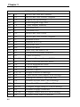
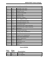
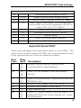
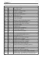
1
POST-Probe PCI
TECHNICAL MANUAL
by
COPYRIGHT © 2005 MICRO 2000, INC.
ALL RIGHTS RESERVED
PRINTED IN USA
MICRO 2000, INC.
1100 E. BROADWAY, 3RD FLOOR
GLENDALE CALIFORNIA 91205
TELEPHONE: (818) 547-0125
FAX: (818) 547-0397
www.Micro2000.com
DOCUMENT #MAN- PP VPCI 10/19/2005
TABLE OF CONTENTS
INTRODUCTION.....................................................................7
About Micro2000 Inc. .......................................................................................... 7
About Post Probe.................................................................................................. 7
Post Probe Features ..............................................................................................8
CHAPTER 1 ............................................................................. 11
Using The POST-Probe.....................................................................................11
Installing the Card................................................................................................11
What do all those lights mean?.........................................................................12
Voltages ..............................................................................................................12
Reset Line...........................................................................................................12
ISA Signals .........................................................................................................13
PCI Signals.........................................................................................................14
Switches ..................................................................................................................14
Stepping Switch ................................................................................................14
DIP Switch.........................................................................................................15
The Hex Display ..................................................................................................16
More Post Code Resources.............................................................................167
CHAPTER 2............................................................................. 18
Diagnostic Procedures........................................................................................18
Using The Codes..................................................................................................18
1.0 Power Supply................................................................................................18
2.0 Motherboard .................................................................................................19
2.1 System BUS...............................................................................................19
2.2 CPU (Central Processing Unit) ............................................................20
2.3 NPU (Numerical Processing Unit) .....................................................20
2.4 Chipset........................................................................................................21
2.5 System Clock..............................................................................................21
2.6 CMOS..........................................................................................................21
2.7 Extended CMOS.......................................................................................22
3.0 Interrupts........................................................................................................22
3.1 Programmable Interrupt Controller (PIC).........................................22
3.2 PIT (Programmable Interval Timer)....................................................23
4.0 BIOS................................................................................................................23
4.1 Boot Load ...................................................................................................23
4.2 BIOS CHECKSUM.................................................................................23
4.3 Password......................................................................................................24
2
Table of Contents
5.0 Memory...........................................................................................................24
5.1 RAM .............................................................................................................24
5.2 Protected Mode.........................................................................................25
5.3 A-20Line......................................................................................................25
5.4 ROM.............................................................................................................26
5.5 ROM Shadow ing.......................................................................................26
5.6 Cache............................................................................................................26
5.7 DMA.............................................................................................................27
6.0 I/O...................................................................................................................27
6.1 I/O Enable.................................................................................................27
6.2 Serial Ports ..................................................................................................27
6.3 Parallel Ports...............................................................................................27
6.4 Hard Drive..................................................................................................28
6.5 Floppy Drive..............................................................................................28
6.6 Miscellaneous I/O....................................................................................28
7.0 Video...............................................................................................................28
7.1 Monochrome Display..............................................................................28
7.2 Color Display .............................................................................................28
7.3 Video ROM ................................................................................................29
7.4 Video RAM.................................................................................................29
8.0 Keyboard........................................................................................................29
8.1 Keyboard Controller ................................................................................29
8.2 A-20 Line.....................................................................................................29
8.3 Keyboard Lock..........................................................................................30
8.4 Turbo Switch..............................................................................................30
9.0 Error Display ................................................................................................30
10.0 Reserved.......................................................................................................30
CHAPTER 3............................................................................. 31
BIOS Post Code Listings...................................................................................31
AMI 2.2 BIOS.......................................................................................................31
AMI Plus BIOS....................................................................................................33
AMI Color.............................................................................................................36
AMI Ez-Flex BIOS.............................................................................................41
AMI Win BIOS....................................................................................................46
AMI Win Boot Block Recovery.......................................................................50
AMI BIOS 8..........................................................................................................51
AMI BIOS 8 Boot Block Initialization..........................................................53
AMI BIOS 8 Boot Block Recovery................................................................53
Award BIOS (original XT)................................................................................54
3
Table of Contents
Award XT Version 3.1 .......................................................................................55
Award Version 3.3...............................................................................................56
Award EISA..........................................................................................................57
Award PnP BIOS.................................................................................................60
Award Elite (Version 4.51 PG)........................................................................62
Award BIOS Version 6.0...................................................................................64
Award 6.0 Quick POST.....................................................................................69
Award 6.0 Boot Block........................................................................................70
COMPAQ General..............................................................................................71
DELL BIOS..........................................................................................................76
HP Pavillion Series 3100 & 8000 PCs............................................................78
HP Vectra BIOS ..................................................................................................84
HP Vectra ES........................................................................................................85
HP Vectra QS & RS............................................................................................89
IBM AT BIOS......................................................................................................92
IBM PS/2 (MCA)................................................................................................95
Intel CA810E BIOS............................................................................................98
Intel CA810E Boot Block Recovery Code...................................................98
Intel CA810E Runtime Code...........................................................................99
Intel CC820 BIOS.............................................................................................104
Intel CC820 Boot Block Recovery................................................................105
Intel CC820 Runtime Code.............................................................................106
Intel SE440BX-2 BIOS....................................................................................111
Intel D810E2CB BIOS....................................................................................116
Intel D810E2CB Boot Block Recovery.......................................................117
Intel D810E2CB Runtime Code....................................................................118
Intel D810EMO BIOS.....................................................................................123
Intel D810EMO Boot Block Recovery.......................................................124
Intel D810EMO Runtime Code....................................................................124
Intel D815BN BIOS.........................................................................................130
Intel D815BN Boot Block Recovery............................................................130
Intel D815BN Boot Block Recovery Continued ......................................131
Intel D815BN Runtime Code........................................................................131
Intel D815EEA BIOS......................................................................................136
Intel D815EEA Boot Block Recovery.........................................................137
Intel D815EEA Runtime Code.....................................................................137
Intel D815EPEA BIOS...................................................................................143
Intel D815EPEA Boot Block Recovery......................................................143
Intel D815EPEA Runtime Code...................................................................144
Intel D820LP BIOS..........................................................................................149
4
Table of Contents
Intel D820LP Boot Block Recovery.............................................................150
Intel SE440BX BIOS........................................................................................156
Intel SR440BX BIOS........................................................................................161
Intel SR440BX Boot Block Recovery..........................................................162
Intel SR440BX Boot Block Recovery Continued .....................................163
Intel SR440BX Runtime Code.......................................................................163
Intel JN440BX BIOS........................................................................................168
Intel LB440GX / LB440GX BIOS..............................................................174
Intel NA440BX / N440BX BIOS................................................................179
Intel RC440BX BIOS.......................................................................................183
Intel RC440BX BIOS Continued ..................................................................184
Intel RC440BX Boot Block Recovery .........................................................184
Intel RC440BX Runtime Code......................................................................185
Phoenix BIOS Plus Version 1.0.....................................................................190
Phoenix PCI BIOS............................................................................................192
Phoenix PCI BIOS, UMC Chipset ...............................................................195
Phoenix ISA / EISA / MCA Version 3.07................................................198
Phoenix BIOS Version 4.0..............................................................................200
Phoenix Version 4 Release 6.0 .......................................................................204
For Boot Block in Flash ROM.......................................................................209
Phoenix Medallion BIOS.................................................................................210
Western Digital BIOS.......................................................................................210
CHAPTER 4........................................................................... 212
BIOS Beep Codes............................................................................................. 212
AMI........................................................................................................................212
Award 4.51...........................................................................................................213
AST........................................................................................................................213
COMPAQ............................................................................................................213
COMPAQ cont’d...............................................................................................214
EURO/MYLEX................................................................................................214
Microid Research ...............................................................................................215
MR BIOS (L=Low Tone, H= High Tone)................................................215
Phillips...................................................................................................................216
Phoenix ISA / EISA / MCA..........................................................................216
Phoenix 4.0 ..........................................................................................................218
QUADTEL .........................................................................................................222
CHAPTER 5........................................................................... 223
POST Procedures............................................................................................. 223
5
Table of Contents
AMI................................................................................................................... 223
Award............................................................................................................... 223
COMPAQ....................................................................................................... 223
HP Vectra........................................................................................................ 224
IBM................................................................................................................... 224
Phoenix ............................................................................................................ 224
CHAPTER 6........................................................................... 225
IBM Error Messages........................................................................................ 225
CHAPTER 7........................................................................... 235
The Legacy POST Probe................................................................................ 235
The Probe............................................................................................................235
Using The Probe................................................................................................236
APPENDIX A......................................................................... 237
APPENDIX B......................................................................... 243
Warranty Information.......................................................................................243
Notes.....................................................................................................................246
Notes.....................................................................................................................247
6
Introduction
About Micro2000 Inc.
Micro 2000 was formed in September 1990 to supply the PC industry
with top-quality diagnostics, which were virtually non-existent at the
time for that segment of the industry. Since then, the company has
maintained its position of leadership through outstanding technical
support and by staying consistently on the cutting edge throughout the
rapid advances in PC technology that continue to occur.
Whether it is PC diagnostic software or hardware, educational materials
or network administrative tools, you can trust all Micro 2000 products
to be state-of-the-art and to be the highest quality products of their
kind available anywhere.
About Post Probe
The Post Probe is the tool to quickly diagnose any IBM-compatible PC
that will not boot up. The Post Probe is a printed circuit card that
plugs into any vacant bus slot on the computer’s motherboard. It can
be used with the ISA bus, EISA, or the newer PCI bus. The Post
Probe monitors the voltages, bus signals, and the computer’s Post, or
Power-On-Self-Test, and shows the results with various LED and 7segment displays.
A computer when powering up will go through a series of steps in the
BIOS to test the computer’s subsystems. As it does each step, it
generates a code for that step, called a POST code. The code varies
according to the manufacturer and version of the BIOS. Post Probe
reads these codes, and if the BIOS fails to get all the way through the
tests, the code displayed will show where the Power-On-Self-Test
halted. There is also a button that allows you to step through the codes
one at a time.
The LED display, the code tables for your type of BIOS (in Chapter 3
of this manual), and the diagnostic procedures in Chapter 2 will allow
you to diagnose the failure, in many cases to the exact component that
7
Introduction
needs to be replaced. Together with Micro 2000’s Micro-Scope
diagnostic software, you will have the arsenal to conquer virtually any
PC computer problem you may encounter.
Post Probe Features
1. PCI CONNECTOR
11. +12 VDC
2. 7-SEGMENT DISPLAY
12. –12 VDC
3. OSC. LED
13. CLK LED
4. RESET LED
14. FRAME/ SMEMR LED
5. ALE LED
15. IRDY/ SMEMW LED
6. STEPPING SWITCH
16. TRDY/ IOW LED
7. VOLTAGE TEST POINTS
17. DEVSEL/ IOR LED
8. 3.3 VDC
18. DIP SWITCH
9. +5 VDC
19. ISA CONNECTOR
10. –5 VDC
8
Introduction
1
2
3 4 5
6
7
8
9
10
11
12
13
14
15
16
17
6
2
18
19
POST-Probe Physical Layout
9
Introduction
Notice: The Post Probe card is designed to be used for
the short period of time that the computer is performing
its Power-On Self Test during boot-up. Leaving the card
inserted into the computer for extended periods of time
may cause the card to be damaged through overheating,
and will void the warranty for the Post Probe.
10
Chapter 1
Using The POST-Probe
Installing the Card
You will notice that the Post Probe card has two edge connectors. One
of these is for the ISA or EISA type bus, and the other is for the newer
PCI bus. If your motherboard has slots for both types of bus, you
should use both. The POST codes will be the same, but the individual
LEDs monitor different signals on each bus. If only one bus is
available, it will be apparent which one to use.
If neither connector fits in the bus slot, you have encountered a third
type, called the MCA bus. MCA stands for “Micro-Channel
Architecture, which is a bus standard developed by IBM for their PS-1
and PS-2 systems. The Post Probe can also be used in this type of bus,
by first plugging the ISA connector into an MCA adapter card, which is
available from Micro 2000.
To install, turn off the computer and open the case. Although not
required, it is usually a good idea to begin by removing all of the
adapter cards plugged into the motherboard’s bus slots in order to
narrow down the source of trouble, because one of these cards could
be shorting out the bus.
Now, orient the Post Probe card so that the row of LEDs are facing up
(for PCI) or toward the front of the computer (for ISA). If there is any
doubt about the orientation of the card, there are arrows adjacent to
each of the connectors. The arrow for the connector in use should be
pointing toward the nearest edge of the motherboard.
Push the Post Probe gently and evenly into a vacant bus slot. When
the card bottoms out in the slot, check along the top edge of the slot to
ensure that the card is straight and even. You may need to remove a
plate or bracket covering the opening at the back of the computer, by
taking out the screw at the top of the bracket. Once the card is
installed, remove your hands and any tools from the computer case,
11
Chapter 1
and turn on the power. The computer will begin its Power-On-SelfTest.
What do all those lights mean?
The Post Probe has two types of displays to tell you what is happening
with signals on the bus. One is the 2-digit HEX display, which we will
cover in a later section. The other is a set of red, green and yellow
LEDs. The green LEDs check the voltages and the red LED monitors
the Reset line. The yellow LEDs each show the status of a different
bus signal.
Voltages
The five green LEDs monitor the DC voltages from the power supply.
Starting from the corner of the card, the voltages are +3.3 VDC, +5
VDC, -5 VDC, +12 VDC and -12 VDC. If a voltage is within a
tolerance of +10% to –5%, the corresponding LED will be lit.
There are also six test points, one for ground and one for each voltage
that allow easy confirmation with a voltmeter.
Note: There is no +3.3 VDC on the ISA bus. The PCI bus does not have –5
VDC, and some PCI models also are missing the +3.3 VDC.
If an LED should be lit and is not, the problem could be the power
supply, the cabling from the power supply, or that the voltage line on
the bus is being shorted out. If none of the LEDs light up, check the
power supply, the main fuse, and the AC into the system.
Reset Line
There is one red LED on the board, located between two yellow LEDs,
about 1½ inches from the edge opposite the ISA connector. This LED
will light anytime the system’s Reset line is activated. This normally
happens only once during boot-up, but you will sometimes see the Post
procedure get to a certain point and then reset, over and over. This
usually means a shorted signal on the motherboard.
12
Using The POST -Probe
ISA Signals
There are seven yellow LEDs that monitor various signals on the bus.
With one exception, they will monitor one function on the ISA bus and
a different function on the PCI bus. The ISA functions are listed here
first.
ALE (Address Latch Enable): This yellow LED (next to the Reset
LED) indicates a signal from the CPU that allows the BIOS to latch
addresses, such as memory addresses. This LED should blink
periodically during the Post. If it does not, the main suspects are the
CPU, the DMA circuit, Bus Controller or the Clock Generator. This
LED has no function on the PCI bus.
I/O READ: This LED will be lit anytime the BIOS tries to read from
an I/O device such as the hard drive, floppy, keyboard etc. If an I/O
device is failing, this will give you a clue whether the fault is with the
device or its controller (light blinks on) or something on the
motherboard such as the BIOS or the DMA chip (light doesn’t go on).
On the backside of the board, this LED is labeled DEVS / IOR.
I/O WRITE: Lights when the BIOS writes to a device, and provides
the same troubleshooting clues as the I/O READ. Labeled TRDY /
IOW.
MEMORY WRITE: BIOS checks RAM by writing to memory and
then reading what was written. This LED blinks during the write. If it
doesn’t, suspect the BIOS or the DMA chip. Label is IRDY /
SMEMW.
MEMORY READ: If MEMORY WRITE blinks but this one
doesn’t, try replacing the RAM. Labeled FRAME / SMEMR.
CLOCK (CLK): This monitors the main system timing signal. It
should blink rapidly and continuously, and may appear to be steady on.
If not lit, check the crystal or the clock generator chip. This signal is
used on both the ISA and PCI, but is not present on the MCA bus in
Micro-channel systems.
13
Chapter 1
OSCILLATOR (OSC): This crystal was the main system timing in
XT machines, but now is just used by the video controller for color
frequency. The signal is not present on the PCI bus. On an ISA bus,
the LED will blink rapidly, and may appear steady on. If not, replace
the 14.138 Mhz crystal. This LED is located next to the Reset LED.
PCI Signals
CLOCK: This is the only signal, other than voltages, monitored in
common with the PCI bus. It should blink rapidly or appear steadily
on.
FRAME: This signal defines the timing window for data transfer on
the bus. The LED should blink repeatedly during Post. If not, the
problem is most likely with the PCI chipset, particularly the bus
controller.
IRDY (Initiator Ready): This LED blinks when the bus recognizes a
device is ready to transfer data. If this function is not working,
problems will be with the PCI chipset.
TRDY (Target Ready): Blinks when the bus recognizes a device is
ready to receive data. Problems could be with the PCI chipset or with
an I/O device.
DEVS (Device Select): This signal shows that a device has been
selected for data transfer. If no blinks, suspect the bus controller.
Switches
Stepping Switch
There are two push-button switches, located at the edges of the card
opposite the connectors. Either of these allow you to step through and
view the POST codes one at a time, in reverse of the sequence in which
they were issued. Just push one of the buttons to progress to the
previous code. There are two buttons so that one of them should be
easily accessible no matter how the Post Probe card is oriented in the
machine.
14
Using The POST -Probe
Please note that the button does not actually cause the Post routines to
execute; rather it shows you the sequence that has already been
executed. This information is valuable because the Post will not always
stop on the section where the error occurred. Sometimes it goes to the
next step before locking up. In other cases, the Post issues its code
only after successful completion of a particular routine. If it doesn’t
complete, the Post will still be showing the code of the previous
routine. If the BIOS has been corrupted, you may even find the Post
executing steps out of sequence, and the stepper switch is the only way
to easily determine exactly what is happening.
DIP Switch
The four-position dual inline pin (DIP) switch on the Post Probe card
sets the I/O port that the card reads to get its Post codes. Most
systems output their codes to I/O Port 80, but there are exceptions, as
noted in the table.
Switch #
1234
Port 80
Port 84
Port 90
Port 190
Port 300
Port 380
Port 680
All Above
Test
1111
0111
1101
1100
1011
1010
1001
1000
0000
Most ISA, EISA & PCI systems (default)
Compaq systems
PS2 models 25 and 30
Any BIOS using Port 190
Award systems with EISA bus
Compaq systems
MCA systems
When in doubt, try this.
Self-diagnostic mode
The settings above represent 0=OFF and 1=ON. This chart is also
silk-screened onto the back of the Post Probe. Be aware there are
some early versions of the card that show 0=ON and 1=OFF.
The self-diagnostic mode will put the display into a continuous loop,
which won’t stop unless it encounters a card malfunction. If this
occurs, contact technical support.
15
Chapter 1
The Hex Display
Each brand and version of BIOS has its own Post routine that it goes
through on boot-up, and each has its own set of codes that it puts out
for the various parts of the Post. Even though all computers are prone
to the same types of problems, the codes will vary and need to be
interpreted. Fortunately however, all BIOS' put out the codes in
hexadecimal format.
These hexadecimal codes are displayed by the 7-segment Hex display.
There are two digits in the display, because most BIOS versions use a
2-digit code. There are certain BIOS' such as the HP Vectra ES, RS and
QS that use a 4-digit code, so the first two digits are displayed
momentarily first, followed by the last two digits of the code.
There is a second hex display on the backside of the Post Probe card.
It displays the same code, but makes it easy to read the codes no matter
which way the card is oriented in the computer.
To find out what a code means, you must locate the table for your
particular BIOS in Chapter 3 of this volume. The tables are in
alphabetical order, by manufacturer. Each table lists the codes for
those BIOS, in numerical order. Once you have found the correct
table, go to the displayed code within that table.
Next to each Post Code number, you will find the manufacturer’s
description of the test, as well as a reference number to a particular
section of the Diagnostic Procedures in Chapter 2. If you then go to
that section of Chapter 2, you will see a detailed analysis of the
hardware being tested in that portion of the Post procedures, and
suggestions to help you isolate and fix the problem.
The tables are extensive, listing over 65 different BIOS versions from
22 manufacturers. However, new BIOS versions are being released all
the time, and several BIOS manufacturers will customize the BIOS for
their customers. For this reason, it is quite possible to encounter a
POST code that is not included in the tables. On the other hand, a
corrupted BIOS can also cause illegitimate Post Codes that are not in
the table.
16
Using The POST -Probe
If the computer is damaged to the extent that Post cannot begin, the
card will display a code of AA. This will usually require replacement of
the BIOS, the CPU or the entire motherboard. The condition can also
occur if an adapter card is shorting out one or more bus signals.
Certain BIOS codes are marked Reserved or OEM-specific. The
BIOS manufacturer will assign these as requested by their customers,
and you will need to contact your system vendor or motherboard
manufacturer to find out what function has been assigned to a
particular reserved code. Codes marked Debug are used by the
manufacturer to test the chips, but are not used during normal POST.
More Post Code Resources
If you come across a code that is not in the table, or a BIOS whose
table is not included in Chapter 3, please check the following websites:
http://bioscentral.com/
http://www.shopctc.com/BiosHelp/Biospostcodes/AMI.htm
http://pchell.com/hardware/beepcodes.shtml
http://computerhope.com/beep.htm
http://uktsupport.co.uk/reference/biosb.htm
If you are still unable to find the code, please contact the Micro2000
Technical Support department. We can help you determine the cause of
the missing code, and you can help us keep our BIOS listing up to date.
17
Chapter 2
Diagnostic Procedures
Using The Codes
Next to each of the POST Codes in Chapter 3 is a Diagnostic Code,
which refers to one of the sections of this chapter. Here you will find a
description of the part of the system that was being tested by that
portion of the POST. Where applicable, there are also suggestions for
further isolating the problem. Appendix A has part numbers of some
of the common motherboard chips for various functions, to help you
locate the specific component.
It does not always mean you should replace that particular component.
Most operations in the system require interaction from several
components, and each can appear to fail if not given correct data or
signals from another part. Also, the POST may not halt on the section
with the defect but on the one immediately before or after. That is why
we've included a button to allow you to step through the POST (see
Stepper Switch in Chapter 1). However, using the POST code
description, Appendix A and the information in this chapter (and
sometimes a little trial and error) will nearly always allow you to
determine the source of the problem.
1.0 Power Supply
Power supply voltages are monitored on the system BUS by the POSTProbe. The voltages supplied are +5V, +12V, -5V, and -12V. On
machines with a PCI BUS, +3.3V is also provided on that BUS. The
LEDs on the POST-Probe corresponding to each voltage will light if
that voltage is within 10% of its proper value. The voltages can also be
tested with a voltmeter on the POST-Probe, measuring between the
test point for the voltage you wish to check and the one marked
ground.
18
Diagnostic Procedures
If all of the voltages are 0, the problem is the power supply, the main
fuse, or the supply of 110VAC to the computer (check the cord to
make sure it's plugged in).
If one or two of the voltages are bad, the cause could be a faulty
supply, or the voltage line on the bus is either open or shorted. Power
off, and unplug all the adapter cards and I/O devices from the
motherboard. Power up and retest the voltage. If it's OK, plug things
back in one at a time (power off when plugging or unplugging, of
course) until the voltage fails. That's your culprit.
If the voltage is still bad with everything unplugged, disconnect the
power supply from the motherboard, and check the voltages on the
power supply connector. If everything checks OK, the problem is on
the motherboard. If not, it's the power supply.
2.0 Motherboard
The motherboard holds the central processing unit (CPU) with its
associated timing and control circuitry, and the system BUS. Also
found here are the jumpers that set the system speed and sometimes
other variables. On the most basic motherboard, everything else
connects to the motherboard either through adapter cards, which plug
into the BUS, or into a special connector on the motherboard.
Check the jumpers to make sure they are seated properly and the
settings are correct. The board itself is seldom a source of failure,
which usually occurs in the on-board circuitry or in one of the devices
attached to the motherboard. If the problem can be isolated to a
particular component, it may be possible to replace that component.
However, on modern motherboards, the trend has been to combine
more and more functions into large-scale integrated chips. For
instance, one 82206 chip now combines the two DMA controllers, the
PITs, the PICs and the RTC, whereas in older systems these were all
separate chips. Many of these large-scale chips are surface-mounted
with special (and expensive) equipment, and the only practical option is
sometimes to replace the entire board.
2.1 System BUS
The bus is the pathway on the motherboard over which information
travels between the CPU, memory, I/O devices, etc. The bus includes
data lines, address lines, voltages and various other signal lines. Those
19
Chapter 2
signal lines, which are monitored directly by the POST-Probe are
described in the Troubleshooting section of Chapter 1. The bus could
also be said to include the bus controller chip and the connectors into
which the various adapter cards are plugged.
The most common bus for most of the PC’s history has been the ISA
(for Industry Standard Architecture) and its close cousins the EISA and
VESA. New systems being sold today nearly always include the faster
PCI bus, which may be used by itself or in combination with an ISA
bus. The signal layouts for these various types of buses are shown in
Appendix B. The USB (Universal Serial Bus) is external to the
motherboard, and is not tested during the Post procedure.
The bus controller chip determines the timing of data transfers,
controls whether it involves memory or I/O, and which way the
transfer is going. A failure of the chip can affect any of these factors.
The PCI and ISA bus will each have its own controller.
About the only other problem that occurs with the bus itself is a
shorted or open signal line, which can cause any number of symptoms
depending on which signal is affected. When bus defects show up in a
system that was previously working, the source will most often be
found in the edge connectors. Remove the adapter cards and inspect
the connectors closely for bent pins or minute metal filings. Keep in
mind that the problem may also be in the bus controller or other chips
connected directly to the bus, or on one of the adapter cards.
2.2 CPU (Central Processing Unit)
The BIOS will try to identify the CPU and will put that ID into the
CMOS. It will then have the CPU execute a series of instructions to
test its functions. If you have just installed a new CPU and retained an
obsolete BIOS, that could be a cause for failure. Otherwise, the
problem is the CPU chip itself, which will have to be replaced.
Fortunately, this chip is usually mounted in a socket or a removable
housing.
2.3 NPU (Numerical Processing Unit)
Also commonly called the Math Coprocessor, this chip handles the
more complicated mathematical functions, which takes some of the
20
Diagnostic Procedures
load from the CPU. Since the 486, the NPU is incorporated into the
CPU. In older systems, the NPU is a separate chip, which is often
impossible to remove and replace without special equipment. On these
systems, replacement of the entire motherboard is the most realistic
option.
2.4 Chipset
This diagnostic code refers to the chip or chips on the motherboard
associated with the BIOS (rather than the video chipset, covered under
code 7.0). Each BIOS version is designed to work best with a
particular chip set. The set would include the PIC, PIT, DMA
controllers, BIOS ROM, CMOS and RTC. These are covered
separately, but if the problem can't be isolated to a particular function,
you will be referred to this code.
If the Chipset Initialization Test fails, you will need the specific
documentation from the motherboard or BIOS manufacturer to isolate
the problem, or else just replace the motherboard.
If the failure is the Chipset Wait State, you can usually cure it by
changing the CMOS wait-state values for the Read, Write, Cache Read,
Cache Write etc. Refer to the BIOS documentation.
2.5 System Clock
There are two aspects of the clock that are tested during the POST.
First are the crystal oscillators. The main crystal generates the timing
frequency for the CPU and Bus. This signal is also indicated by the
CLOCK LED on the POST-Probe card. There is a second 14.318
crystal, which was the original system clock but is now just used by the
PIT and video circuits. The other part is the RTC (Real Time Clock)
chip, which generates the date and time information (this chip also
usually contains the CMOS memory cells: see next section). You
should be able to tell from the POST code description, which is being
tested. Do not confuse any of these with the operating system clock.
DOS and Windows both keep track of the date and time, but not until
the system has successfully booted up.
2.6 CMOS
This is a section of non-volatile memory, meaning it holds its contents
even when the computer is turned off, because of a long-life CMOS
21
Chapter 2
battery that provides it power. Among other things, this memory holds
the date and time, RAM configuration, information about the
peripheral devices such as their IRQ and DMA assignments, disk drive
parameters, whether the computer will start up in Real or Protected
Mode, etc.
The CMOS is usually contained in the RTC chip. Any number of
hardware or software glitches can corrupt the values stored in CMOS
in ways that can prevent boot-up. The POST will check values stored
in CMOS against data it receives from other system components, and
any mismatch can cause the POST to lock up. If you can determine
the incorrect value, try changing it manually through CMOS Setup and
restart the computer, before replacing any hardware. If the POST
continues to fail or CMOS cannot maintain its contents, the problem
may be the chip but more likely will be the CMOS battery or its
connections.
The battery may be inside the RTC chip or an external lithium battery.
Some HP systems power the CMOS with a capacitor rather than a
battery.
2.7 Extended CMOS
Newer (and more complex) systems have more variables (such as PnP)
than can be stored in the normal RTC chip, and use a chip, which has
an additional 2K of CMOS memory. This is labeled XCMOS.
3.0 Interrupts
The most common problem with interrupts during the POST is that
two I/O devices are set to the same IRQ, or interrupt request level.
Remove the most recently installed adapter card. The system will
probably boot up and you can then use the Micro-Scope Diagnostic
software to find out which IRQs are already in use. Jumpers on the
card will allow you to change to a vacant IRQ, and you can then reinstall the device. The table in Appendix A shows the allocated and
available IRQs.
3.1 Programmable Interrupt Controller (PIC)
The chips that control the interrupt traffic between the CPU and
various hardware devices are called Programmable Interrupt
Controllers, or PICs. Each PIC can control eight interrupt lines,
22
Diagnostic Procedures
designated IRQ 0 through IRQ 7. To achieve the 16 interrupt levels
required by all PCs since the 286, the chips are cascaded by connecting
the output of a second chip to the IRQ 2 input of the first chip. The
original IRQ 2 is routed to IRQ 9 on the second chip. Any adapter
card that is set to IRQ 2 is actually using IRQ 9. Some POST routines
will tell you which of the two PIC chips or even which IRQ line is
failing, but others just indicate a PIC failure.
3.2 PIT (Programmable Interval Timer)
This chip controls the timing of CPU interrupt sequences, and failure
can show up in several places in any POST version. On older systems
(286) it was also involved in the basic system timing, and could be a
suspect in benchmarking errors.
4.0 BIOS
(Basic Input-Output System) These are the hard-coded instructions,
contained in ROM on the motherboard, that the computer uses to get
started. The BIOS executes the POST routine that tests various
components and parameters of the system (and generates the POST
codes). The BIOS also includes the boot loader (see 4.2).
4.1 Boot Load
As its last step, the BIOS will look for a bootable operating system and
turn control of the CPU over to it. Most commonly, it will look first to
the floppy drive and then to the hard drive. If a boot load error occurs,
the BIOS has been unable to complete this function. The most likely
causes are hardware failure of the drive or a missing boot routine.
Before making any drastic repairs, first remove any floppy diskettes and
see if the system boots to the hard drive. Then, insert a floppy known
to contain a boot loader, and try booting again. If neither works, you
might suspect a corrupt BIOS.
4.2 BIOS CHECKSUM
When all of the data in the BIOS ROM is added up, another figure is
created called a checksum, which will cause the total to roll over to all
zeroes. The POST does this addition all over again, and a quantity
other than zero indicates that one or more bits of the ROM code have
23
Chapter 2
changed, and therefore the BIOS is corrupted. Often, a corrupted
BIOS will not get far enough into the POST to give this indication.
4.3 Password
A few BIOS versions will check to see if a password is stored in
CMOS. This is not necessarily a problem, because the motherboard will
usually have a switch or jumper that allows you to disable the password,
which you can re-enter once the system has booted up.
5.0 Memory
Memory refers to storage of information in a way that is readily
accessible to other parts of the system. This distinguishes it from disk
drives, CDROM, etc. These devices also store information, but it
must be loaded into system memory before it can be used.
The first megabyte of memory is called conventional memory, and was
the maximum memory size of the first PCs. It is divided into base
memory (the first 640 kilobytes) and the upper memory area (between
640k and 1 megabyte, abbreviated as UMA). Everything above 1
megabyte is called extended memory. In some older systems, there
may be a section of UMA referred to as EMS, for Expanded Memory
Specification.
5.1 RAM
Random Access Memory is found on narrow cards (modules) plugged
into the motherboard. The chips on theses modules are Dynamic
RAM or DRAM chips, meaning they must be periodically supplied
power on a Refresh line in order to retain their data. RAM contents are
lost whenever the system power is turned off.
Each individual chip can store from 64K to 256M bits of data. In one
common configuration, each chip will provide 1 bit of data at a time to
the system, and 8 chips on the module make up a byte. If there is a 9th
chip, it provides the parity bit. Some DRAM chips output 4 or 8 bits at
a time and will therefore have only 1 or 2 chips per module (plus
parity). In all cases, the quantity and capacity of the chips used
determines how many megabytes of memory are contained in that
module. The cards are either SIMMs (Single In-line Memory Modules,
24
Diagnostic Procedures
with 30 or 72 pins) or DIMMs (Dual In-line Memory Modules, with
168 pins). All of the SIMMs or DIMMs in a bank must be the same
size.
Most POST routines will first determine the amount of memory
present, and check to see that the amount found agrees with the switch
settings and CMOS values. Then they will thoroughly test the first
64K, partially test memory above 64K, and test the refresh signal,
which is an intermittent voltage supplied to the RAM chips. Some
BIOS' will also test each data line and address line individually, which
greatly aids troubleshooting. If so, this info will be found in Chapter 3
under the POST code listings for that BIOS. See Appendix A for
memory allocations.
Memory may be mapped in different ways from one system to the next.
If the system won't boot up because of memory failure and you don't
know the mapping strategy in use, the low-tech solution is to get one
SIMM or DIMM of the same capacity presently used in the system, and
swap out each module in turn until the problem disappears. If the
symptoms persist, the problem is most likely with the signals coming to
the module: the address lines, data lines, voltages or refresh signal.
There is also memory-mapping circuitry on the motherboard which
may have failed.
5.2 Protected Mode
The first PCs only had one megabyte of memory, and operated in what
is now called Real Mode. Protected mode allows modern operating
systems to run in memory above 1 MB. CPUs still have the option to
run in Real Mode for backward compatibility, and the POST will switch
from one to the other. If this test fails, the culprit is usually the CPU
chip or the A-20 Line (see 5.3).
5.3 A-20Line
Address lines A-0 through A-19 access the first megabyte of memory.
Address line A-20 is the first line allowing access to extended memory,
and must be enabled and disabled as the CPU switches between Real
and Protected Mode. Because the 286 CPU did not have circuitry to
control this, the IBM engineers routed A-20 through some unused pins
on the 8042 Keyboard Controller chip, and it can still be found there
25
Chapter 2
on many systems. On other systems, this function will be found
elsewhere on the motherboard. Refer to the documentation to find
exactly where. A failure may be indicated as an A-20 test, or as part of
the Protected Mode tests.
5.4 ROM
Read-Only Memory will be found on many adapter cards, and on the
mother board itself for the BIOS. If a POST code just refers to ROM
it almost always means adapter-card ROM. The POST will start at
memory address C800:0000 and check in 2K increments for a value of
55AA hex, which indicates a device is using that section of ROM. The
POST will then execute the initialization program for the device,
starting at the fourth byte of that section.
If the POST stops during the ROM test, you must isolate which device
is causing the problem. Starting with the most recently added device,
remove the adapter cards one at a time until the problem disappears. It
may be a defective I/O device or its adapter card, but often is just a
problem with the setup of the device. Common errors are two devices
both trying to use the same section of memory, or set to the same IRQ
or DMA values.
5.5 ROM Shadowing
Most systems have the ability to move ROM code into RAM, where it
can be accessed much faster. If this test fails, disable ROM shadowing
in the CMOS, and turn it back on a portion at a time. Start by enabling
shadowing for the BIOS ROM, then Video ROM. If the System Setup
allows, enable shadowing by the other adapter cards one at a time until
the culprit is found. The cure could be either the card's ROM or the
RAM for that memory section. As a quick fix, you may be able to just
leave shadowing disabled for that device.
5.6 Cache
In 486 and later processors, the CPU has internal cache memory for
faster access to frequently needed RAM contents. This is Level 1
Cache, and if it fails, the CPU is defective. Additional cache is
provided by static SRAM chips external to the CPU, called Level 2
Cache. Some new CPUs have Level 2 cache in CPU, and call it Unified
26
Diagnostic Procedures
Cache. With a Level 2 Cache failure, either the SRAM or CPU is
defective, or the system expects external cache but none is installed.
5.7 DMA
Direct Memory Access. Allows data transfers to and from memory
without monopolizing the CPU. All systems since the 286 use two
cascaded DMA chips to provide 15 DMA channels, or a VLSI chip that
combines DMA with the PIT, PIC and RTC functions. You may get a
POST code for DMA, but you should also suspect the DMA if RAM
fails and can't be fixed by swapping the memory modules.
6.0 I/O
(Input/Output): This covers any devices, which send information to
and from the motherboard, except for the video and keyboard, which
are covered separately. This includes the floppy and hard drives, and
the serial and parallel ports. Most BIOS routines do not test the CDROM or sound cards.
6.1 I/O Enable
A few POSTs will test the ability to enable and disable an integrated
I/O Controller.
6.2 Serial Ports
The POST will search for serial ports, and then test them. An error
shows that a port was found, and that a problem was detected with it.
Most systems have serial ports designated COM1 and COM2, and the
POST may tell you which was being tested. It may also refer to an
RS232 test. Older systems will have serial controllers that can be
replaced, but most newer systems have a large-scale integrated I/O
controller surface-mounted on the motherboard.
6.3 Parallel Ports
An error indicates that the POST found a parallel port, but it was not
functioning properly. The problem is usually the I/O controller. Older
systems will have a parallel controller card, but on most newer systems,
it will be part of an integrated I/O Controller on the motherboard.
27
Chapter 2
6.4 Hard Drive
The POST will first query the controllers and compare to what the
CMOS says should be there. It may then do a seek test of each drive,
to the last cylinder and then to the first. The problem may be the drive
or the controller, but it could also be the CMOS values. If you can
load a diagnostic disk such as Micro-Scope, you can better pin-point
the failure area.
6.5 Floppy Drive
The BIOS will initialize and test the floppy drive. As with the hard
drive, a failure could be the controller, the drive, or corrupted CMOS.
6.6 Miscellaneous I/O
Many newer BIOS will test the dedicated mouse port, and a few will
check for a game port. If the mouse port fails, make sure the mouse is
plugged in (and doesn't have the keyboard plugged into that port). The
game port may fail because no controller is dedicated to that port, and
you will have to disable or remove the port in order to pass the POST.
Refer to the system docum entation for instructions.
7.0 Video
The POST may interrogate the Video Card to see what kind of monitor
is installed. If the test fails, most likely the monitor is not connected or
doesn't match CMOS parameters.
7.1 Monochrome Display
The BIOS may separately initialize the monochrome and color control
circuitry, as a holdover from the days when color monitors were a
novelty. If the controllers are actually separate, they will be found on
the motherboard rather than on a video adapter card.
7.2 Color Display
See 7.1, Monochrome Display.
28
Diagnostic Procedures
7.3 Video ROM
The POST looks for a value of 55AAh at memory location C000:0000,
and will then run the program located at C000:0003. If this test fails, it
will probably be a faulty video card, but it could also be that the video
card identified in CMOS does not match the one installed in the
system.
7.4 Video RAM
The amount of system RAM allotted to video is not enough for today's
graphic-intensive programs so video adapters will have their own RAM
located on the adapter card itself. If this test fails, replace the video
card.
8.0 Keyboard
The POST will see if it can detect the keyboard, and will also test the
keyboard controller. If the keyboard is not detected, make sure it is
plugged in, and then check the connector. As a last resort, swap out
the keyboard, which may be defective or may just need a good cleaning.
8.1 Keyboard Controller
The keyboard controller chip (8042, 8742) is located on the
motherboard and controls serial data transfers to and from the
keyboard, often including the reset signal to the CPU. The controller
uses IRQ1 for keystroke data coming in from the keyboard, and stores
the keystrokes in an internal buffer until the interrupt is recognized by
the CPU.
Some POST routines run extensive tests of the keyboard functions, but
any failure still comes down to replacing either the keyboard or the
controller chip.
8.2 A-20 Line
One line of the keyboard controller is often used to control Address
line 20. More information on this is available under section 5.2,
PROTECTED MODE.
29
Chapter 2
8.3 Keyboard Lock
For security, some systems come with a keyboard lock that prevents
the system from accepting keyboard input. This is a physical lock,
turned with a key and usually mounted on the front of the case, but
sometimes on the keyboard. Only a few BIOS versions test this.
8.4 Turbo Switch
On some systems, POST will check this switch, usually located on the
front of the case next to the Reset switch. The switch has no function
on 486 or higher CPUs.
9.0 Error Display
If errors occur during the POST, many BIOS versions will
attempt to put a message on the monitor screen telling you
what failed. If the system is functioning well enough for the message
to arrive on the screen, consider yourself lucky. Most of these error
messages are self-explanatory, but IBM PC and PS/2 systems send a 6digit code. These codes are listed at the end of the BIOS codes
chapter.
10.0 Reserved
Certain POST codes are marked Reserved or OEM-specific. The
BIOS manufacturer will assign these as requested by their customers,
and you will need to contact your system vendor or motherboard
manufacturer to find out what function has been assigned to a
particular reserved code.
Codes marked Debug are used by the manufacturer to test the chips,
but are not used during normal POST.
30
Chapter 3
BIOS POST Code Listings
AMI 2.2 BIOS
Post
Code
00
03
06
09
0C
0F
12
15
18
1B
1E
21
24
27
2A
2D
30
33
36
39
3C
3F
Diag.
Sect.
2.2
2.2
2.4
4.2
5.7
3.2
3.2
5.7
5.7
3.1
3.2
3.2
5.1,5.7
5.1
8.1
2.6
5.2
5.1
5.2
5.2
2.5
8.0
Description
Flag Test
Register Test
Chipset Test
BIOS Checksum
Page Register
8254 Timer
Memory Refresh
DMA Controllers
8237 DMA Initialization
8259 Initialization
PIC Chips
Memory Refresh (1st Bank)
Base 64 Address test
Base 64 Memory test
8742 Keyboard Chip
MC146818 RTC/CMOS
Protected Mode
Size Memory
Protected Mode
Protected Mode Failed
CPU Speed Calculation
Read 8742 Hardware Switches
31
Chapter 3
42
45
48
4B
4E
51
54
57
5A
5D
60
63
66
69
6C
6F
72
75
78
7B
7E
81
84
87
8A
8D
90
93
96
32
3.1
2.6
7.0
3.1
5.2
8.1
8.1
8.1
8.1
8.1
8.1
8.1
5.2
5.1, 5.7
5.1
5.5
5.1
2.6
2.6
4.0, 5.7
3.2
2.5, 2.6
8.0
8.0
8.0
3.1
2.3
6.2
6.3
AMI 2.2 BIOS Continued
Initialize Interrupt Vector Area
Verify CMOS Configuration
Test & Initialize Video System
Unexpected Interrupt Test
Start 2nd Protected Mode Test
Verify LTD Instruction
Verify TR Instruction
Verify LSL Instruction
Verify LAR Instruction
Verify VERR Instruction
Address Line 20 Test
Unexpected Exception Test
Start 3rd Protected Mode Test
Address Line Test
System Memory Test
Shadow Memory Test
Extended Memory Test
Verify Memory Configuration
Display CMOS Error Messages
Copy System BIOS Shadow Memory
8254 Clock Test
MC146818 RTC Test
Keyboard Test
Determine Keyboard Type
Stuck Key Test
Initialize Hardware Interrupt Vector
Math Coprocessor
Determine COM Ports Available
Determine LPT Ports Available
BIOS POST Code Listings
99
9C
9F
A2
A5
A8
AE
AF
B1
2.6, 4.0
6.4, 6.5
6.5
6.4
5.4
8.3
2.6
4.1
4.1
AMI 2.2 BIOS Continued
Initialize BIOS Data Area
Fixed/Floppy Controller Test
Floppy Disk Test
Fixed Disk Test
External ROM Scan
System Key Lock Test
F1 Error Message Test
System Boot Initialization
Interrupt 19 Boot Loader
AMI Plus BIOS
Post
Diag.
Code
Sect.
00
01
02
03
04
05
06
07
08
09
0A
0B
0C
0D
0E
10
4.1
2.6
2.2
4.2
3.1
2.6, 3.1
3.2
3.2
5.7
5.7
5.7
5.7
5.7, 3.2
5.7, 3.2
5.7, 3.2
5.1
Description
Control To Interrupt 19
NMI Disabled (Bit 7 of I/O Port 70h).
286 Register Test Over
ROM Checksum OK
8259 Initialization OK
CMOS Interrupt Disabled
System Timer Counting OK
CH-0 of 8259 Test OK
CH-2 of Delta Count Test OK
CH-1 of Delta Count Test OK
CH-0 of Delta Test Count OK
Parity Status Cleared
Refresh & System Time OK
Refresh Link Toggling OK
Refresh Period ON/OFF 50% OK
About to Start 64K Memory
33
Chapter 3
11
12
13
14
15
16
17
18
19
1A
1B
1C
1D
1E
1F
20
21
22
30
31
32
33
34
35
36
37
38
39
3A
34
5.1
5.1
5.1, 4.0
8.1
2.6
2.6
7.1
7.2
7.3
7.3
7.4
7.4
7.0
7.0
7.0, 2.6
7.0
7.0
7.0, 2.6
5.1
5.2
5.2
5.1
5.1
5.1
5.1
5.1
5.1
5.1
5.1
AMI Plus BIOS Continued
Address Line Test OK
64K Base Memory Test OK
Interrupt Vectors Initialized
8042 Keyboard Controller
CMOS Read/Write Test OK
CMOS Checksum/Battery check
Monochrome Mode Set OK
Color Mode Set OK
Video ROM Search
Optional Video ROM Control OK
Display Memory Read/Write Test OK
Alternate Display Memory OK
Video Retrace Check OK
Global Byte set for Video OK
Mode Set for Mono/Color OK
Video Test OK
Video Display OK
Power On Message Display OK
Virtual Mode Memory Test
Virtual Mode Memory Test Started
Processor in Virtual Mode
Memory Address Line Test
Memory Address Line Test
Memory Below IMB Calculated
Memory Size Computation OK
Memory Test in Progress
Memory Initialization Over below 1MB
Memory Initialization Over above 1MB
Display Memory Size
BIOS POST Code Listings
3B
3C
3D
3E
3F
40
41
42
4E
4F
50
51
52
53
54
55
56
57
58
59
5A
5B
5C
5D
5E
5F
70
71
72
5.1
5.1
5.1
5.2
5.2
8.1
8.1
5.7
2.1
5.2
5.7
5.7
5.7
5.7
5.7
5.7
5.7
3.1
3.1
3.1
3.2
3.2
3.2
3.2
3.2
3.2
8.1
8.1
8.1
AMI Plus BIOS Continued
About To Start below 1MB
Memory below 1MB OK
Memory above 1MB OK
About to go to Real Mode
Shutdown Successful
About to Disable Gate A-20
Gate A-20 Disabled
About to test DMA Controller
Address Line Test OK
Processor In Real Mode
DMA Page Register Test OK
DMA Unit-1 Base Register
DMA Unit-1 Channel Register OK
DMA Channel-2 Base register Test OK
About to test Latch for Unit-1
F/F Latch Tests both Units OK
DMA Units 1 & 2 programmed OK
8259 Initialization Over
8259 Mask Register Check OK
Master 8259 Mask Register OK
Check Timer & Keyboard Interrupt
Timer Interrupt OK
About to test Keyboard Interrupt
ERROR! Timer/Keyboard Interrupt
8259 Interrupt Controller Error
8259 Interrupt Controller Test OK
Start of Keyboard Test
Keyboard Bat Test OK
Keyboard Test OK
35
Chapter 3
73
74
75
76
77
79
7A
7B
7D
7E
7F
80
81
82
83
84
85
86
87
00
8.1
6.5
6.5
6.4
6.4
2.6
2.6
2.6
5.1
5.1
7.3
8.1
5.4
6.3
6.2
2.3
9.0
4.0
4.0
AMI Plus BIOS Continued
Keyboard Global Data Initialize
Floppy Setup about to start
Floppy Setup OK
Hard Disk Setup about to start
Hard Disk Setup OK
About to Initialize Timer Data
Verify CMOS Battery Power
CMOS Battery Verification Done
Analyze Test Results for Memory
CMOS Memory Size Update OK
Check Optional ROM C000:0
Keyboard Sensed to Enable Setup
Optional ROM Control OK
Printer Global Data Init. OK
RS-232 Global Data Init. OK
80287 Check/Test OK
About to display Soft Error
Give Control to System ROM E000
System ROM E000 Check Over
Call to Interrupt 19 for boot loader
AMI Color
Post
Code
00
01
02
03
04
05
36
Diag.
Sect.
4.1
2.2
3.2
2.4
8.1
2.6
Description
Control to Int 19 Boot Loader
CPU Test
Power-On Delay
Chipset Initialization
Soft/Hard Reset
ROM Enable
BIOS POST Code Listings
06
07
08
09
0A
0B
0C
0D
0E
0F
10
11
12
13
14
15
16
17
18
19
1A
1B
20
21
22
23
24
25
26
4.2
8.1
8.1
8.1
8.1
8.2
8.1
2.6
2.6
2.6
2.5, 2.6
3.1, 5.7
3.1, 5.7
5.1
3.2
3.2
3.2
3.2
3.2
3.2
3.2
3.2
5.1
5.1
5.1
5.1
5.1
8.4
8.4
AMI Color Continued
ROM BIOS Checksum
8042 Test
8042 Test
8042 Test
8042 Test
8042 Protected Mode Test
8042 Test
8042 Test, CMOS
CMOS Checksum
CMOS Initialization
CMOS/RTC Status
DMA/PIC Disable
DMA / PIC Initialization
Chipset/Memory Initialization
8254 Timer Test
CH-2 Timer Test
CH-1 Timer Test
8254 CH-0 Test
Memory Refresh Test
Memory Refresh Test
Check 15-microsecond Refresh
Check 30-microsecond Refresh
Base 64K Memory Test
Base Memory Parity Test
Memory Read/Write
BIOS Vector Initialization
BIOS Vector Initialization
Turbo Check of 8042
Global Data Table for Turbo
37
Chapter 3
27
28
29
2A
2B
2C
2D
2E
2F
30
31
32
33
34
35
36
37
38
39
3A
40
41
42
43
44
45
46
47
48
49
38
2.6, 7.0
7.1
7.2
7.4
7.3
7.3
2.6
7.4
7.4
7.0
7.4
7.0
7.0
7.0
4.0
2.6
2.6
2.6
2.6
2.6
5.2
4.0, 5.1
5.2
3.2, 5.2
5.1
5.1
5.1
5.1
5.1
5.1
AMI Color Continued
Video Mode Test
Monochrome Test
Color Test
Parity Enable Test
Optional ROM Check Start
Video ROM Check
Reinitialize Chipset
Video Memory Test
Video Memory Test
Video Adapter Test
Alt. Video Memory Test
Alt. Video Adapter Test
Video Mode Test
Video Mode Set
BIOS ROM Data Area
Power-On Message Display
Power-On Message Display
Read Cursor Position
Display Cursor Reference
Display Hit <ESC> Message
Protected Mode Start
Build Descriptor Tables
Protected Mode Entry
Protected Interrupt Enable
Check Descriptor Tables
Size Memory
Memory Read/Write Test
Base 640K Memory Test
640K Memory Size
Extended Memory Size
BIOS POST Code Listings
4A
4B
4C
4D
4E
4F
50
51
52
53
54
55
56
57
58
59
60
61
62
63
64
65
66
67
80
81
82
83
84
85
5.1
8.1
5.7
2.6, 5.1
2.6, 5.1
5.1
2.6, 5.1
5.1
5.1
5.2
4.0
5.2
3.2, 5.1
3.2, 5.1
2.6
2.4
5.7
5.7
5.7
3.2, 5.1
3.2, 5.1
5.7
3.1
8.1
8.1
8.1
8.1
8.3
8.3
2.6
AMI Color Continued
Extended Memory CMOS Verify
Check for Soft/Hard Reset
Clear Extended Memory
Update CMOS on Memory Size
Base RAM Displayed
Memory Read/Write Test on 640K
Update CMOS on RAM Size
Extended Memory Test
Re-size Extended Memory
Re-enter Real Mode
Restore CPU Registers
A-20 Gate Disabled
BIOS Vector Recheck
BIOS Vector Half Checked
Clear Hit <ESC> Message
DMA, PIT Test
DMA Page Register Test
DMA #1 Test
DMA #2 Test
BIOS Data Area Check
BIOS Data Area Halfway Point
Initialize DMA Chips
8259 Initialization
Keyboard Test
Keyboard Reset
Stuck Key and Batch Test
8042 Reset
Lock Key Check
Compare Memory Size with CMOS
Password/Soft Error Check
39
Chapter 3
86
87
88
89
8A
8B
8C
8D
8E
8F
90
91
92
93
94
95
96
97
98
99
9A
9B
9C
9D
9E
9F
A0
A1
A2
A3
40
2.6
2.6
2.4
2.6
2.6
2.6
2.6
6.4, 6.5
2.6, 6.5
6.5
2.6, 6.4
6.4
3.2, 5.1
3.2, 5.1
2.6, 5.1
7.0
3.2, 5.7
7.0
3.2, 5.7
2.5, 3.2
6.2
3.2, 5.7
2.3
3.2, 5.7
8.1
8.0
8.1
5.6
2.6
2.6, 8.0
AMI Color Continued
XCMOC/CMOS Equipment Check
CMOS Setup Entered
Reinitialize Chipset
Display Power-On Message
Display Wait and Mouse Check
Shadow any Option ROMs
Initialize XCMOS Settings
Reset Hard/Floppy Drives
Floppy Compare to CMOS
Floppy Initialization
Hard Disk Compare to CMOS
Hard Disk Initialization
BIOS Data Table Check
BIOS Data Check at halfway
Set Memory Size
Verify Display Memory
Clear Interrupts
Optional ROM Check
Clear Interrupts
Setup Timer Data/RS232 Base
RS232 Test
Clear Interrupts
NPU Test
Clear Interrupts
Extended Keyboard Check
Set Numlock
Keyboard Reset
Cache Memory Test
Display Soft Errors
Set Typematic Rate
BIOS POST Code Listings
A4
A5
A6
A7
A8
A9
AA
00
2.6
2.6
2.6, 5.7
3.2, 5.7
2.6, 5.1
3.2, 5.7
2.6
AMI Color Continued
Memory Wait States
Clear Screen
Enable Parity/NMI
Clear Interrupts
Control to E000
Clear Interrupts
Display Configuration
Call to Interrupt 19 for boot loader
AMI Ez-Flex BIOS
Post
Code
01
02
03
04
05
06
07
08
09
0A
0B
0C
0D
0E
0F
10
11
12
Diag.
Sect.
2.2
1.0
2.4
8.1
5.4
4.2
8.1
8.1
8.1
8.1
5.2, 8.2
8.1
2.7
2.6
2.6
2.5, 2.6
3.1, 5.7
7.0
Description
Disable NMI, Start CPU Flag Test
Power-On Delay
Initialize Chipset
Keyboard Hard/Soft Reset
ROM Enable
ROM BIOS Checksum
8042 Keyboard Controller Test
8042 Keyboard Controller Test
8042 Keyboard Controller Test
8042 Keyboard Controller Test
Test 8042 Protected Mode
8042 Keyboard Controller Test
Test CMOS RAM Shutdown Register
Test CMOS Checksum
Initialize CMOS
CMOS/RTC Status OK
Disable DMA and PIC
Disable Video Display
41
Chapter 3
13
14
15
16
17
18
19
1A
1B
20
21
22
23
24
25
26
27
28
29
2A
2B
2C
2D
2E
2F
30
31
32
33
42
2.4, 5.0
3.1
3.2
3.2
3.2
3.2, 5.0
3.2, 5.0
3.2, 5.0
5.0
5.0
5.0
5.0
3.0
3.0
8.1
8.1
3.0
7.1
7.2
5.0
5.4
7.3
7.2
7.4
7.4
7.0
7.4
7.0
7.0
AMI Ez-Flex BIOS Continued
Initialize Chipset and Memory
8254 PIC Tested
PIT Channel 2
PIT Channel 1
PIT Channel 0
PIT Memory Refresh
PIT Memory Refresh
Check PIT 15 Microsecond Refresh
Test Base 64K Memory
Test Address Lines
Test Base 64K Parity
Test Memory Read/Write
Setup Prior to Vector Table Initialization
Initialize Vector Table in Lower 1K of RAM
Test 8042 Keyboard Controller
Keyboard Controller Global Function
Setup for Vector Table Initialization
Test Video Monochrome Mode
Test Video Color Mode (CGA)
Test Parity Enable
Check for Optional ROMs
Check for Video ROM
Check for EGA/VGA
Test Video Memory (non-EGA/VGA)
Test Video Memory
Test Video Adapter
Test Alternate Video Memory
Test Alternate Video Adapter
Test Video Mode
BIOS POST Code Listings
34
35
36
37
38
39
3A
40
41
42
43
44
45
46
47
48
49
4A
4B
4C
4D
4E
4F
50
51
52
53
54
55
7.0
4.0
1.0
1.0
7.0
7.0
7.0
5.2
2.7
5.2
5.2
2.7
5.0
5.0
5.0
5.0
5.0
4.0, 5.5
5.0
5.0
2.6, 5.0
5.0
5.0
5.0, 5.5
5.0
5.2
2.2, 5.2
2.2
5.3
AMI Ez-Flex BIOS Continued
Test Video Mode
Initialize BIOS ROM Area
Set Power-On Display Cursor
Display Power-On Message
Read Cursor Position
Display Cursor Reference
Display Setup Message
Protected Mode Tested
Build Descriptor Tables
CPU in Protected Mode
Enable Protected Mode Interrupt
Check Descriptor Tables
Check Memory Size
Memory Read/Write Test
Test Base 640KB of RAM
Check for Memory Below 1MB
Check for Memory Above 1MB
Check BIOS ROM Data Area
RAM Below 1MB Cleared for Soft Reset
RAM Above 1MB Cleared for Soft Reset
Update CMOS Memory Size
Display Base 64KB Memory Test
Test Base 640KB Memory
RAM Size Update for Shadowing
Test Extended Memory
System Prepared for Real Mode
Return CPU to Real Mode
Return CPU Registers to Real Mode
Disable A-20 Gate
43
Chapter 3
56
57
58
59
60
61
62
63
64
65
66
67
80
81
82
83
84
85
86
87
88
89
8A
8B
8C
8D
8E
8F
90
91
44
5.5
5.5
7.0
5.7
7.4
5.7
5.7
5.5
5.5
5.7
3.1
8.0
8.0
8.0
8.1
8.3
2.6, 5.0
4.3
2.6
2.6
2.4
1.0, 7.0
6.6
5.5
2.6
6.1
2.6, 6.5
6.5
2.6, 6.4
6.4
AMI Ez-Flex BIOS Continued
BIOS Data Area Re-Checked
BIOS Data Area Check Complete
Display Set-up Message
DMA Register Page Test
Verify Display Memory
Test DMA #1
Test DMA #2
BIOS Data Area Check
BIOS Data Area Check Complete
Initialize DMA
Initialize 8259 PIC
Keyboard Test
Keyboard Reset
Stuck Key and Batch Test
Test 8042 Keyboard Controller
Check Lock Key
Compare Memory Size to CMOS
Check Password and Soft Error
CMOS Equipment Check
CMOS Setup
Initialize Chipset
Display Power-On Message
Check Mouse and Display Wait Message
Attempt to Shadow Option ROMs
Initialize System with CMOS Settings
Reset Hard Drives and Floppy Drives
Compare Floppy Setup to CMOS Settings
Initialize Floppy Controller
Compare Hard Drive to CMOS Settings
Initialize Hard Drive Controller
BIOS POST Code Listings
92
93
94
95
96
97
98
99
9A
9B
9C
9D
9E
9F
A0
A1
A2
A3
A4
A5
A6
A7
A8
A9
AA
00
2.7, 4.0
2.7, 4.0
2.6, 5.0
7.4
3.0
5.4
3.0
3.1
6.2
3.0
2.3
3.0
8.0
8.1
8.0
2.2, 5.0
5.0
8.0
5.0
7.0
3.0, 5.0
3.0
5.4
3.0
2.6, 7.0
4.1
AMI Ez-Flex BIOS Continued
Check BIOS Data Table
BIOS Data Table Check Complete
Set Memory Size
Verify Display Memory
Clear All Interrupts
Check for Optional ROMs
Clear All Interrupts
Timer Data Setup
Check for Serial Ports
Clear All Interrupts
Check Math Co-Processor
Clear All Interrupts
Extended Keyboard Check
Set Numlock on Keyboard
Keyboard Reset
Test Cache Memory Size
Display Any Soft Errors
Set Typematic Rate
Set Memory Wait States
Clear Display
Enable Parity and NMI
Clear All Interrupts
Give System Control to ROM at E0000
Clear All Interrupts
Display Configuration
Call Boot Loader Int. 19
45
Chapter 3
AMI Win BIOS
Post
Code
00
01
02
03
05
06
08
08
0A
0B
0C
0D
0E
0F
10
11
12
13
14
19
1A
20
23
24
25
26
27
28
46
Diag.
Sect.
4.1
2.6
8.1
8.1
5.6
4.0, 5.1
2.6
2.6
2.6
2.4
8.1
8.1
8.1
8.1
8.1
8.1
2.4
2.4
3.2
3.2, 5.1
3.2, 5.1
5.1
4.0, 5.1
2.2, 5.1
2.7, 8.4
8.4
2.2, 2.4
2.6
Description
Control to Int 19 Boot Loader
Disable NMI
Power-On Delay
Soft Reset Power-On
Disable Cache
Uncompressed POST Code
CMOS Checksum
CMOS Initialization
CMOS Initialization for Date and Time
Initialization Before Keyboard Batch
Batch Command to Keyboard Controller
Verify Batch Command
Initialize After KB Controller Batch
Write KB Command Byte
Pin 23/24 Block/Unblock Command
Check For <INS> Key Command
DMA/PIC Disable
Chipset Initialization
8254 Timer Test
Memory Refresh Test
Check 15 Micro-Second Refresh
Base 64 Test
Set BIOS Stack Before Int. Vector Init.
Interrupt Vector Initialization
Read Input of 9042 Chip, Clear Password
Initialize Global Data for Turbo Switch
Initialize before setting Video Mode
Set Video Mode
BIOS POST Code Listings
2A
2B
2C
2D
2E
2F
30
31
32
34
37
38
39
3A
3B
40
42
43
44
45
46
47
48
49
4B
4C
4D
4E
4F
50
2.1
7.3
7.3
2.3
2.3
5.1, 7.0
7.0
5.1, 7.0
7.0
7.0
7.0
2.1, 2.4
2.4, 7.0
7.0
5.2
2.2, 2.4
5.2
2.7, 3.1
5.1
5.1, 5.2
5.1
5.1
5.1
5.1
2.6, 8.1
5.1
2.6, 4.0
5.1
5.1
2.7, 7.0
AMI Win BIOS Continued
Initialize BUS (Sys,Static, Output Dev.)
Setup before Operational Video Check
Control to Optional Video ROM
Proc. after Optional Video ROM Routine
Display Mem R/W Test if No EGA/VGA
Display Memory R/W Test
Retrace Check
Display Alternate Memory R/W Test
Alternate Display Retrace Check
Set Display Mode
Display Power-On Message
Init. BUS Types (Input, IPL, Gen Devices)
Display BUS Initialization Error Messages
Display the Hit <DEL> Message
Virtual Mode Memory Test
Prepare Descriptor Tables
Enter Virtual Mode for Memory Test
Enable Interrupts for Diagnostic Mode
Initialize Data to Check Mem. Wrap At 0:0
Check Mem. Wrap, Find Total RAM
Memory Write Test
640K Base Memory Write Test
Determine Memory Below 1 MB
Determine Memory Above 1 MB
Check for Soft Reset, clear Mem below 1 MB
Clear Memory Above 1 MB
Save Memory Size
Display First 64K Memory Size
Sequential and Random Memory Test
Displayed Memory Size
47
Chapter 3
51
52
53
54
57
58
59
60
62
65
66
67
7F
80
81
82
83
84
85
86
87
88
89
8B
8C
8D
8E
8F
91
94
48
5.1
2.6, 5.1
2.2, 5.2
5.2
5.7
8.1
3.1, 5.7
5.7
5.7
2.7, 5.7
3.1
8.1
8.1
8.1
8.1
8.1
8.3
2.6
2.6
2.6
2.6
2.6
7.0
2.7, 7.3
2.4
2.7, 6.2
6.4
6.5
6.4
2.6
AMI Win BIOS Continued
Above 1MB Memory Test
Save Memory Size Information
Enter Real Mode
Disable Gate A-20 Line
Adjust Memory Size
Clear Hit <DEL> Message
DMA/PIC Test
DMA #1 Base Register Test
DMA #2 Base Register Test
Program DMA Unit 1 and 2
Initialize 8259 Interrupt Controller
Keyboard Test
Enable Extended NMI Sources
Stuck Key and Batch Test
Keyboard Controller Test
Write Command Byte, Init. Circular Buffer
Lock Key Check
Compare Memory Size with CMOS
Password/Soft Error Check
Programming Before Setup
Execute CMOS Setup
Programming After Setup
Power-On Display
Shadow Main and Video BIOS
Setup Options After CMOS Setup
Initialize Mouse
Reset Hard Disk Controller
Floppy Setup
Hard Disk Setup
Base/Extended Memory Size
BIOS POST Code Listings
95
96
97
98
99
9A
9B
9C
9D
9E
9F
A0
A1
A2
A3
A4
A5
A7
A8
A9
AA
B0
B1
C2
C5
C6
C7
C8
CA
CB
2.1
2.1
5.4
2.4
2.4
6.2
2.4
2.3
2.4
8.1
8.1
2.6, 8.1
5.6
7.0
2.7, 8.1
2.4, 2.7
2.7, 5.1
2.4
5.4
2.4
2.7, 7.0
2.7, 4.0
5.1
2.4, 2.7
2.7
4.2
2.7
2.6
2.5, 2.6
2.4
AMI Win BIOS Continued
Init. PCI/VLB BUS Optnl ROMs from C800
Initialize Before C800 Optnl ROM Control
Control to Optional ROM
Processing After Optional ROM Control
Setup Timer Data Area/Printer Base Address
Set RS-232 Base Address
Initialize Before NPU Test
NPU Initialization
Initialization After NPU Test
Check Extended KB, KB ID and Num -Lock
Issue Keyboard ID Command
Reset Keyboard ID Flag
Cache Memory Test
Display any Soft Errors
Set the Keyboard Typematic Rate
Program Memory Wait States
Clear Screen, Enable Parity NMI
Init. Needed Before Control to E000 ROM
Control to E000 ROM
Init. Needed After Control to E000 ROM
Display System Configuration
Uncompressed SETUP Code for Hot-Key
Copy any Code to Specific Area
Disable NMI, Power-On Delay
Enabel ROM, Disable Cache
ROM BIOS Checksum
CMOS Shutdown Register Test
CMOS Checksum
Initialize CMOS Date and Time
Initialization Before Keyboard Batch
49
Chapter 3
CD
CE
CF
D1
D2
D3
D4
D5
DD
8.1
8.1
8.1
8.1
3.1, 5.7
2.4, 5.1
4.0, 5.1
4.0
4.0, 5.1
AMI Win BIOS Continued
BAT Command to Keyboard Controller
Installation After KB Controller Batch
Write Keyboard Command Byte
Check for <INS> Key Command
Disable DMA and Interrupt Controllers
Chipset Initialization/Auto Detect Memory
Uncompressed RUNTIME Code
RUNTIME Code Uncompressed
Control to Shadow RAM at F000:FFF0
AMI Win Boot Block Recovery
Note: These codes should only appear if a malfunction occurs while updating the
BIOS flash ROM.
Post
Code
E0
E1
E2
E6
ED
EE
EF
F0
F1
F2
F3
F4
F5
FB
FC
FD
50
Description
Initialize Floppy Controller, Test Base RAM
Initialize Interrupt Vector Table
Initialize Interrupt and DMA Controllers
Enable Floppy, IRQs and Internal Cache
Initialize Floppy Drive
Read First Sector of Drive A
Read Error, Drive A
Search for AMIBOOT.ROM in Root Dir.
AMIBOOT.ROM not found in Root Dir.
Reading FAT to Find AMIBOOT.ROM
Reading AMIBOOT.ROM File
Incorrect Size for AMIBOOT.ROM
Disable Internal Cache
Detecting ROM Type
Erasing Flash ROM
Programming Flash ROM
BIOS POST Code Listings
FF
AMI Win Boot Block Recovery Continued
Programming Done, Restart BIOS
AMI BIOS 8
Post
Code
00
03
04
05
06
08
0A
0B
0C
0E
13
24
2A
2C
2E
30
31
33
37
38
39
3A
3B
3C
40
Diag.
Sect.
4.1
2.6, 3.0
2.6
3.1
3.2
2.2
8.1
6.x
8.0
6.6
2.4
4.0
2.1, 7.4
7.3
6.1
2.1
6.6
7.1
7.3
2.1
2.7
2.5
5.1
2.4
2.3, 6.1
Description
Control to Int 19 Boot Loader
Disable NMI, Initialize CMOS
Verify CMOS Checksum
Initialize PIC and Int Vector Table
Initialize System Timer
Initialize CPU
Initialize Keyboard Controller
Detect PS/2 Mouse
Detect Keyboard
Init Input Devices, Update Kernel Variables
Initialize Chipset Registers
Start Platform-specific BIOS Modules
Initialize PCI bus and any Video Devices
Initialize Video Adapter and ROM
Initialize All Output Devices
Initialize System Management Interrupt
Activate ADM Module
Setup to Display Text Information
Display Sign-on and CPU info
Configures PnP and PCI Devices
Initialize DMAC
Initialize RTC Date and Time
Test for Total Memory, Display Total.
Mid-Post Initialization of Chipset Registers
Detect Ports, NPU
51
Chapter 3
50
52
60
61-70
75
78
7A
7C
84
85
87
8C
8D
8E
90
A0
A1
A2
A4
A7
A8
A9
AA
AB
AC
B1
C0
C1
C2
C5
52
5.1
2.6
8.0
6.4
4.1
5.4
2.1
9.0
9.0
4.0
2.4
1.0
3.0
2.1
4.3
4.1
3.0
7.1
2.2
2.2
9.0
3.0
4.1
2.4
1.0
2.2, 5.6
4.1
4.1
AMI BIOS 8 Continued
Adjust for Memory Ho les
Update CMOS Memory Total
Set NumLock and Keyboard Rate
OEM-specific Errors
Initialize Int 13 (for Disk I/O)
Initializes IPL (Boot) Devices
Initialize Remaining ROM
Write PnP Data to RAM
Log POST Errors
Display Errors
Execute BIOS Setup if Needed
Late-Post Initialization of Chipset Registers
Build ACPI Tables (if ACPI pwr mgmt supp)
Set NMI
Init. System Management Interrupt
Check Boot Password, if Installed
Cleanup Before Boot to OS
Initialize IRQ Routing Table
Initialize Runtime Language Module
Initialize CPU, Display Sys Config Screen
Prepare CPU for Boot
Wait for User Response to Config, if Needed
Uninstall Int 09 and 1C Vectors
Prepare BIOS Boot Spec. for Int 19 Boot
End of Post Initialization of Chipset Registers
Save Sys Context for ACPI Power Mgmt
Disable Cache, Early CPU Initialization
Setup Boot Processor Info
Set Boot Processor for POST
Setup Application Processors
BIOS POST Code Listings
C6
C7
5.6
2.2
AMI BIOS 8 Continued
Re-enable Cache
Exit Early CPU Initialization
AMI BIOS 8 Boot Block Initialization
Note: These codes will appear while updating the BIOS flash ROM.
Post
Code
Before D1
D1
D0
D2
D3
D4
D5
D6
D7
D8
D9
DA
E1-E8
EC-EE
Description
Early Chipset Initialization and Super I/O Initialization
Is done. NMI Disabled.
Keyboard Controller Test. Check Power Mgmt
Wakeup. Save Power-on CPUID in Scratch CMOS.
Verify Boot block Checksum.
Disable Cache, Size Memory.
Additional Chipset Initialization, Enable Cache
Test Base 512K RAM.
Copy Boot block to RAM.
Test BIOS Checksum, Test Forced BIOS Recovery
Restore CPUID.
Runtime Module Uncompressed into RAM.
Copy Main BIOS Into RAM.
Restore CPUID. Give Control to BIOS POST.
OEM-specific Errors. Reserved for Chipset and
System Manufacturers.
AMI BIOS 8 Boot Block Recovery
Note: These codes should only appear if a malfunction occurs while updating the
BIOS flash ROM.
Post
Code
Description
E0
Initialize Floppy, DMA and PIC
53
Chapter 3
E9
EA
EB
EF
F0
F1
F2
F3
F5
FA
FB
F4
FC
FD
FF
AMI BIOS 8 Boot Block Recovery Continued
Setup Floppy Controller, Attempt Read
Enable ATAPI, Read from CD-ROM
Disable ATAPI
Read Error
Search for Recovery File in Root Directory
Recovery File Not Found
Analyze FAT to Locate Recovery File Clusters
Read Recovery File, Cluster by Cluster
Disable L1 Cache
Compare Recovery File to Flash ROM
Verify Flash ROM Part.
Recovery File Size Does Not Match Flash Part Size
Erase Flash ROM
Program Flash ROM
Flash Update OK. Disable Flash Write. Restore CPUID.
Award BIOS (original XT)
Post
Code
03
06
09
0C
0F
12
15
18
1B
1E
54
Diag.
Sect.
2.2, 2.5
2.2, 2.5
2.4
4.2
5.7
5.7
5.7
3.2
3.2
3.2, 5.7
Description
Flag Register Test
CPU Register Test
System Hardware Initialization
BIOS Checksum
DMA Page Register Initialization
Test DMA Address and Count Registers
DMA Initialization
Timer Test
Timer Initialization
Start RAM Refresh
BIOS POST Code Listings
21
24
27
2A
2D
30
33
36
39
3C
3F
42
45
48
4B
4E
54
55
57
5A
Award BIOS (original XT) Continued
5.1
Test Base 64K of RAM
3.1
Setup Init and Temp Stack
3.1
Initialize PIC
3.2
Interrupt Mask Register Test
3.1, 3.2
Hot Interrupt Test
2.3, 5.7
V40 DMA if present
2.4
Verify System Clock Initialization
8.1
Keyboard Test
2.4, 5.1
Set up Interrupt Table
2.0
Read System Configuration Switches
7.0
Video Test
6.2
Serial Port Determination
6.3
Parallel Port Determination
6.0
Game Port Determination
7.0
Copyright Message Display
2.5
Calculation of CPU Speed
5.1
Test of System Memory
6.5
Floppy Drive Test
6.4, 6.5
System Initialized Before Boot
4.1
Call to Int 19
Award XT Version 3.1
Post
Code
01
02
06
07
09
0A
Diag.
Sect.
2.2, 2.5
2.4
2.4
2.2
4.2
7.0
Description
Processor Test
Type of POST/Keyboard Buffer
Initialize 6845, 8237, 59, 53
Process Registers
ROM Checksum
Initialize the Video
55
Chapter 3
15
16
17
18
19
1A
1E
1F
20
21
22
2C
2D
2F
31
FF
Award XT Version 3.1 Continued
5.1
Test First 64K Memory Bank
3.1
Set Up Interrupt Tables
7.0
Set Up Video
7.4
Test Video Memory
3.1
8259 Mask Bits-Channel 1
3.1
8259 Mask Bits-Channel 2
5.1
Size Memory
5.1
Test Base Memory
3.1
Test Stuck 8259s
3.1, 3.2
Test Stuck NMI
6.5
Initialize Floppy Drive
6.2
Initialize COM Ports
6.3
Initialize LPT Ports
2.3
Initialize Math Coprocessor
5.4
Initialize Option ROMs
4.1
Int. 19 Boot Attempt
Award Version 3.3
Post
Code
01-05
06
07
08-0E
0F
10-14
15
16
17
18
56
Diag.
Sect.
8.1
2.4
2.2
2.4
2.7
3.2
5.1
4.0
7.0
7.0
Description
Keyboard Controller
On-board LSI
CPU
CMOS, 8254, 8237, 8259, EPROM
Extended CMOS
Refresh
First 64K RAM
Interrupt Vector Tables
Video Initialization
Video Memory
BIOS POST Code Listings
19
1A
1B
1C
1D
1E
1F
20-23
24
25
26
27
28
29
2A
2B
2C
2D
2E
2F
30
31
D0-EF
FF
Award Version 3.3 Continued
3.1
Interrupt Line Mask
3.1
Interrupt Line Mask
2.6
Battery Good
2.6
CMOS Checksum
2.6
CMOS Chip
5.1
Memory Size
2.1, 5.1 Memory Verifier
2.4
CPU Support Chips
5.1
Extended Memory Size
5.1
Extended Memory Test
5.2
Protected Mode
5.5, 5.6 Shadow RAM, Cache controller
5.5, 5.6 Shadow RAM, Cache Controller
10.0
Reserved
8.1
Initialize Keyboard
6.5
Floppy Drive Initialization
6.2
Serial Port Initialization
6.3
Parallel Port Initialization
6.4
Hard Disk Initialization
2.3
Math Coprocessor
10.0
Reserved
5.4
Optional ROMs
10.0
Reserved
4.1
Boot
Award EISA
Post
Code
01
02
Diag.
Sect.
2.2, 2.5
2.2
Description
CPU Flags
CPU Registers
57
Chapter 3
03
04
05
06
07
08
09
0A
0B
0C
0D
0E
0F
10
11
14
15
16
17
18
19
1F
20
21
22
23
24
25
26
27
58
2.4
3.2
8.1
4.2
2.6
5.1
5.6
2.6, 5.1
2.6
8.1
7.0
7.4
5.7
5.7
5.7
3.2
3.1
3.1
3.1
3.1
3.1
2.7
2.6, 5.4
2.6, 5.4
2.6, 5.4
2.6, 5.4
2.6, 5.4
2.6, 5.4
2.6, 5.4
2.6, 5.4
Award EISA Continued
Initialize DMA, PIC, PIT
Memory Refresh
Keyboard Initialization
ROM Checksum
CMOS, Battery
256K Memory
Cache
Set Interrupt Table
CMOS Checksum
Keyboard Initialization
Video Adapter
Video Memory
DMA Channel 0
DMA Channel 1
DMA Page Register
Timer Chip
PIC Controller 1
PIC Controller 0
PIC Stuck Bits
PIC Maskable IRQs
NMI Bit Check
CMOS XRAM
Slot 0
Slot 1
Slot 2
Slot 3
Slot 4
Slot 5
Slot 6
Slot 7
BIOS POST Code Listings
28
29
2A
2B
2C
2D
2E
2F
30
31
32
3C
3D
3E
3F
41
42
43
45
47
4E
4F
50
51
52
53
60
61
62
63
2.6, 5.4
2.6, 5.4
2.6, 5.4
2.6, 5.4
2.6, 5.4
2.6, 5.4
2.6, 5.4
2.6, 5.4
5.1
5.1
2.7
2.6
2.6, 6.2
5.6
5.4
6.5
6.4
6.2
2.3
2.6
2.0
4.3
2.6
2.4
5.4
2.5, 2.6
5.1
5.6
8.1
4.1
Award EISA Continued
Slot 8
Slot 9
Slot 10
Slot 11
Slot 12
Slot 13
Slot 14
Slot 15
Memory Size 256K
Memory Test Over 256K
EISA Memory
CMOS Setup
Mouse/Adapter, CMOS
Cache RAM
Shadow RAM
Floppy Drive
Hard Drive
RS232 Parallel
NPU
Speed
Manufacturing Loop
Security
CMOS Update
Enable NMI, Cache
Adapter RO Ms
Set Time
Virus Protection Setup
Boot Speed
Num Lock Setup
Boot
59
Chapter 3
B0
B1
BE
BF
C0
C1
C2
C3
C4
C5
C6
C8
C9
CA
FF
5.2
3.2
2.4
2.4
5.6
5.1
5.1
5.1
2.6, 7.0
2.7, 5.5
2.6, 5.6
2.4
2.7, 5.5
2.4
4.1
Award EISA Continued
NMI In Protected
Disable NMI
Chipset Default Initialization
Chipset Program
Cache On/Off
Memory Size
Base 256K Test
DRAM Page Select
Video Switch
Shadow RAM
Cache Program
Speed Switch
Shadow RAM
OEM Chipset
Boot
Award PnP BIOS
Post
Code
03
05
07
09
0A
0B
0C
0D
0E
0F
10
60
Diag.
Sect.
4.0, 5.1
8.1
2.6
2.4
2.2
2.4, 5.1
2.6, 5.1
2.4, 5.1
2.4
5.7
5.7
Description
Initialize EISA Registers
Keyboard Controller Self-Test
Verify CMOS R/W
OEM Specific Initialization
Issue CPU ID Instruction
PnP Initialization
Initialization of BIOS Data Area
Program Some of Chipset's Value
Initialize APIC (Multi-processor BIOS Only)
DMA Channel 0 Test
DMA Channel 1 Test
BIOS POST Code Listings
11
14
15
16
19
1E
30
31
32
3C
3D
3E
41
42
43
45
4E
4F
50
52
53
60
61
62
63
B0
B1
BE
BF
C0
5.7
3.2
3.1
3.1
3.1
5.4
5.1
5.1
2.6, 4.0
2.6, 4.0
8.1
2.4, 5.6
6.5
6.4
6.2, 6.3
2.3
2.6
2.6
2.6, 5.1
5.4
2.5, 5.1
5.1
2.6, 5.6
8.1
4.1
2.4, 5.2
2.4
2.6
2.4
2.4
Award PnP BIOS Continued
DMA Page Registers Test
Test 8254 0 Counter 2
Test 8259 Interrupt Mask Bit For Channel 1
Test 8259 Interrupt Mask Bit For Channel 1
Test 8259 Functionality
If An EISA NVM
Get Size of Base and Extended Memory
Test Base and Extended Memory
Test All On-Board Super I/O Ports
Set Flag to allow CMOS Setup Utility
Install PS2 Mouse
Try To Turn On Level 2
Initialize Floppy Controller
Initialize Hard Drive Controller
Initialize Serial & Parallel Ports
Initialize Math Coprocessor
Show all Error Messages On Screen
Ask For Password, if needed
Write all CMOS Values currently In BIOS
Initialize all ISA ROMs
If not PnP BIOS, Initialize Ports
Set Up Virus Protection
Try to turn on Level 2 Cache
Program Num Lock & Typematic Speed
Boot System via Int 19h
Unexpected Interrupt in Protected Mode
Unclaimed NMI occurred
Program Defaults into Chipset
Program remaining Chipset Values
Init. all Standard Devices with Defaults
61
Chapter 3
C1
C3
C5
FF
Award PnP BIOS Continued
Auto-detect On-Board DRAM & Cache
Test First 26K DRAM
Copy ROM BIOS to E000-FFFF
System Booting
5.1, 5.6
5.1
4.0, 5.1
4.1
Award Elite (Version 4.51 PG)
Post
Code
01
02
03
04
05
07
08
09
0A
0B
0C
0D
0E
0F
10
11
14
15
16
17
18
19
62
Diag.
Sect.
2.2
2.2
2.4
3.2, 5.1
7.0, 8.1
2.6
5.1
2.2, 5.6
5.1
2.6
8.1
7.0
7.4
5.7
5.7
5.7
3.2
3.1
3.1
3.1
3.1
3.1
Description
Processor Test 1
Processor Test 2
Initialize Chipset
Test Memory Refresh Toggle
Blank Video, Initialize Keyboard
Test CMOS Interface and Battery
Set Up Low Memory
Early Cache Initialization
Set Up Interrupt Vector Table
Test CMOS RAM Checksum
Initialize Keyboard
Initialize Video Interface
Test Video Memory
Test DMA Controller 0
Test DMA Controller 1
Test DMA Page Registers
Test Timer Counter 2
Test 8259-1 Mask Bits
Test 8259-2 Mask Bits
Test Stuck 8259 Interrupt Bits
Test 8259 Interrupt Functionality
Test Stuck NMI Bits (Parity I/O Check)
BIOS POST Code Listings
Award Elite (Version 4.51 PG) Continued
1A
2.2, 2.5
Benchmark
1F
2.7
Set EISA Mode
20-2F 2.4, 5.4
Enable Slots 0-15
30
5.1
Size Base and Extended Memory
31
5.1
Test Base and Extended Memory
32
2.7
Test EISA Extended Memory
3C
2.6
Setup Enabled
3D
6.2
Initialize and Install Mouse
3E
5.6
Set Up Cache Controller
41
6.5
Initialize Floppy
42
6.4
Initialize Hard Drive
43
6.2, 6.3
Detect & Init. Serial & Parallel Ports
45
2.3
Detect & Init. Math Coprocessor
4E
2.0
Mfg. POST Loop, or Display Messages
4F
4.3
Security Check
50
2.6
Write CMOS
51
2.4
Pre-Boot Enable
52
5.4
Initialize Option ROMs
53
2.5, 2.6
Initialize Time Value
60
5.1
Set Up Virus Protect
61
5.6
Set Boot Speed
62
8.1
Set Up NumLock
63
4.1
Boot Attempt
B0
8.1
Spurious
B1
3.2
Unclaimed NMI
BE
2.4
Chipset Default Initialization
BF
2.4
Chipset Initialization
C0
2.4, 5.6
Turn Off Chipset Cache
C1
5.1
Memory Presence Test
C5
5.5
Early Shadow
63
Chapter 3
C6
E1-F
FF
Award Elite (Version 4.51 PG) Continued
5.6
Cache Presence Test
5.1
Setup pages. E-1 = page1, E-2 = page 2, etc
4.1
Boot
Award BIOS Version 6.0
Same as Phoenix Medallion BIOS
Post
Diag.
Code
Sect.
01
5.5
02
03
04
05
06
07
08
09
0A
0B
0C
0D
0E
0F
10
11
12
13
14
15
10.0
2.0
10.0
2.6
10.0
8.1
8.1
10.0
6.6, 8.0
10.0
10.0
10.0
5.5
10.0
2.4
10.0
2.6
10.0
2.4
10.0
64
Description
Expand x-group codes in RAM at 1000:0. (Note:
01 is the 7th step of POST, not the 1st. It follows C, C0,
C1, C3 and C5 in that order.)
Reserved
Initialize Superio_Early_Init Switch
Reserved
Clear CMOS Error Flag, Blank Out Screen
Reserved
Clear 8042 Interface, Start 8042 Self-Test
Test Super I/O Keyboard Controller
Reserved
Detect Keyboard and Mouse Ports
Reserved
Reserved
Reserved
Test Shadowing Capability
Reserved
Auto-Detect for DMI Support
Reserved
Test CMOS Memory, Set RTC Status
Reserved
Set Chipset Default Values
Reserved
BIOS POST Code Listings
16
17
18
19
1A
1B
1C
1D
1E
1F
20
21
22
23
24
25
26
27
28
29
2A
2B
2C
2D
2E
2F
30
31
32
33
Award BIOS Version 6.0 Continued
2.0
Set Early_Init_Onboard_Generator Switch
10.0
Reserved
2.2
Detect CPU Data
10.0
Reserved
10.0
Reserved
3.0
Initialize IRQ Vector Table
10.0
Reserved
2.6
Set Early_PM_Init Switch
10.0
Reserved
8.0
Load Keyboard Matrix (Notebook Only)
10.0
Reserved
1.0
Initialize HPM (Notebook Only)
10.0
Reserved
2.6
Load CMOS Settings into BIOS Stack
10.0
Reserved
10.0
Reserved
10.0
Reserved
3.1
Initialize Int. 9 Buffer
10.0
Reserved
2.2, 2.4
Initialize CPU and Chipset
10.0
Reserved
10.0
Reserved
10.0
Reserved
7.0
Display BIOS and CPU Info Onscreen
10.0
Reserved
10.0
Reserved
10.0
Reserved
10.0
Reserved
10.0
Reserved
8.0
Reset Keyboard
65
Chapter 3
34
35
36
37
38
39
3A
3B
3C
3D
3E
3F
40
41
42
43
44
45
46
47
48
49
4A
4B
4C
4D
4E
4F
50
51
66
Award BIOS Version 6.0 Continued
10.0
Reserved
10.0
Reserved
10.0
Reserved
10.0
Reserved
10.0
Reserved
10.0
Reserved
10.0
Reserved
10.0
Reserved
3.2
Test 8254 PIT Chip
10.0
Reserved
3.1
Test 8259 PIC Channel 1 Bits
10.0
Reserved
3.1
Test PIC Channel 2 Bits
10.0
Reserved
10.0
Reserved
3.1
Test PIC Functionality
10.0
Reserved
10.0
Reserved
10.0
Reserved
2.1
Initialize EISA Slot
10.0
Reserved
5.0
Calculate Memory Size
10.0
Reserved
10.0
Reserved
10.0
Reserved
10.0
Reserved
2.2
Initialize CPU and Cache
10.0
Reserved
6.6
Initialize USB
10.0
Reserved
BIOS POST Code Listings
52
53
54
55
56
57
58
59
5A
5B
5C
5D
5E
5F
60
61
62
63
64
65
66
67
68
69
6A
6B
6C
6D
6E
6F
Award BIOS Version 6.0 Continued
5.0
Test Extended Memory
10.0
Reserved
10.0
Reserved
2.2
Display Number of Processors
10.0
Reserved
2.1
PNP Initialization
10.0
Reserved
2.7
Initialize Anti-Virus
10.0
Reserved
7.0
Optional Display Message
10.0
Reserved
6.6
Initialize Super I/O and Audio Switch
10.0
Reserved
10.0
Reserved
2.7
OK to Enter Setup Utility
10.0
Reserved
10.0
Reserved
10.0
Reserved
10.0
Reserved
6.6
Initialize PS/2 Mouse
10.0
Reserved
3.0, 5.0
Setup Memory Size Interrupt 15h
10.0
Reserved
2.2, 5.0
Turn On L2 Cache
10.0
Reserved
2.4
Program Chipset Registers
10.0
Reserved
2.1
Assign Resources to ISA PNP Devices
10.0
Reserved
6.5
Initialize Floppy Controller
67
Chapter 3
70
71
72
73
74
75
76
77
78
79
7A
7B
7C
7D
7E
7F
80
81
82
83
84
85
86
87
88
89
90
91
92
93
68
Award BIOS Version 6.0 Continued
10.0
Reserved
10.0
Reserved
10.0
Reserved
4.0
Test for AWDFLASH.EXE
10.0
Reserved
6.4
Detect/Install IDE Devices
10.0
Reserved
6.2, 6.3
Detect Serial and Parallel Ports
10.0
Reserved
10.0
Reserved
2.3
Initialize Coprocessor
10.0
Reserved
10.0
Reserved
10.0
Reserved
10.0
Reserved
7.1
Switch to Text mode
10.0
Reserved
10.0
Reserved
1.0, 4.3
Enable Power Mgt, Check for Password
2.6
Save Stack Data to CMOS
2.1, 5.4
Initialize ISA PNP Boot Devices
3.0
Assign IRQs to PCI Devices
10.0
Reserved
10.0
Reserved
10.0
Reserved
10.0
Reserved
10.0
Reserved
10.0
Reserved
10.0
Reserved
4.1
Read Boot Sector for Antivirus Code
BIOS POST Code Listings
94
95
96
C0
C1
C3
C5
CF
FF
Award BIOS Version 6.0 Continued
2.2, 5.0
Final Initialization, Enable L2 cache
2.5, 8.0
Update Keyboard and Daylight Savings
2.5
Load RTC Date/Time into DOS Tick Timer
2.4
Early Chipset Initialization. This and next four
codes actually occur at the beginning of POST, in
order of CF, C0, C1, C3 and C5.
2.2, 5.0
Detect Memory and Cache
5.5
Decompress BIOS Code into DRAM
5.5
Shadow BIOS
2.6
Test CMOS Red/Write Functions
4.1
Boot Attempt
Award 6.0 Quick POST
These codes will appear if the Quick Boot option is set in CMOS. This
option does a shorter version of POST and is recommended for dayto-day operation but not if there are hardware problems.
Post
Code
65
66
67
68
69
6A
6B
Diag.
Sect.
2.4,
6.6,
8.1
2.2,
3.0,
5.0,
2.6,
8.0
7.4
3.0
5.0
2.1,
2.2,
6.1,
Description
Initialize Onboard Devices and Keyboard
Controller, Reset Chipset Registers
Check CPUID. Initialize Cache and Interrupt
Vectors
Verify CMOS and Battery. Initialize Keyboard and
BIOS Data Area
Initialize Video Adapter, Test Video RAM
Initialize 8259 Channel 1, Mask IRQ 9
Quick Memory Test
Detect CPU Speed, Initialize Onboard Super I/O,
Display PnP Data and Vendor-specific text. Setup
Virus Protection.
69
Chapter 3
6C-6F
70
71
72
74
75
76
77
78
79-7C
7D
7E
7F
80
FF
1.0,
3.0
5.0
6.5
2.3
6.4
4.3,
9.0
2.6,
5.4
6.4
4.1
8.1
3.0
4.1
Award 6.0 Quick POST Continued
Reserved
Initialize Mouse and ACPI Subsystem, Install
Interrupt Vectors, Display Setup Message
Initialize Cache Controller
Initialize Floppy Controller and Drives
Initialize NPU
Test Hard Drive Write Protection
Reserved
Display POST Errors, Check Password
Write CMOS Values to RAM, Enable Parity,
Initialize Option ROMs
Reserved
Boot Partition Head/Cylinder Values to RAM
Final Initialization
Set NumLock Status and System Speed
Set Low Stack, call Int 19h
Boot
Award 6.0 Boot Block
Used when updating Flash BIOS ROM
Post
Code
01
05
12
0D
41
FF
70
Description
Clear Base Memory
Initialize Keyboard Controller
Initialize Interrupt Vectors
Initialize Video
Initialize Floppy and Onboard Super I/O
Load Boot Sector
BIOS POST Code Listings
COMPAQ General
Post
Code
00
01
02
03
04
05
06
08
09
0A
0B
0C
0D
0E
0F
10
11
12
13
14
15
16
17
18
19
1A
1B
1C
Diag.
Sect.
2.2
2.0
8.1
8.1
5.4
5.4
2.6, 8.1
3.1
2.6
8.1,8.2
8.1, 8.2
2.6, 8.1
3.2
3.2
8.1
3.2
7.0
7.0
3.2
3.2
2.6
2.6
2.6
5.1
5.1
7.0
4.0
2.6
Description
Initialize Flags, MSW, IDTLIN
Read Manufacturing Jumper
8042 received Read Command
No response From 8042
Look for ROM at E000
Look for ROM at C800
Normal CMOS Reset Code
Initialize 8259, 80287
Reset Code in CMOS Byte
Vector Vis 40:67 Reset Function
Vector Vis 40:67 With E01 Function
Boot Reset Function
Test #2 8254 Counter 0
Test #2 8254 Counter 2
Warm Boot
PPI Disabled, PITs 0 and 1
Initialize (blast) VDU Controller
Clear Screen; Turn ON Video
Test Time 0
Disable RTC Interrupts
Check Battery Power
Battery Has Lost Power
Clear CMOS Diags.
Test Base Memory (First 128k)
Initialize Base Memory
Initialize VDU Adapters
The System ROM
CMOS Checksum
71
Chapter 3
1D
1E
1F
20
21
22
23
24
25
26
27
28
29
2A
2B
2C
2D
2F
30
31
32
33
34
35
36
37
38
39
3A
3B
72
5.7
8.1
5.25.
5.1
2.5
2.33
8.1
2.5, 8.2
6.5
6.4
6.3
5.4
2.6, 5.4
7.0
2.5
5.4
3.2
2.6
5.1
3.1, 4.0
3.1, 4.0
2.6
2.6
2.6
2.6
5.4
6.2
6.3
5.4, 8.1
8.1
COMPAQ General Continued
DMA Controller/Page Registers
Test Keyboard Controller
Test 286 Protected Mode
Test Real and Extended Memory
Initialize Time-of-Day
Initialize 287 Coprocessor
Test the Keyboard and 8042
Reset A20, Set Default CPU Speed
Test Diskette Subsystem
Test Fixed Disk Subsystem
Initialize Parallel Printer
Perform Search for Optional ROMs
Test Valid System Configuration
Clear Screen
Check for Invalid Time and Date
Optional ROM Search
Test Timer 2
Write to Diag. Byte
Clear First 128k Bytes of RAM
Load Interrupt Vectors 70-77
Load Interrupt Vectors 00-1F
Initialize MEMSIZE and RESETWD
Verify CMOS Checksum
CMOS Checksum is Not Valid
Check Battery Power
Check for Game Adapters
Check for Serial Ports
Check for Parallel Printer Ports
Initialize Port and Comm Time-outs
Flush Keyboard Buffer
BIOS POST Code Listings
40
41
42
43
44
45
46
47
50
51
52
53
54
55
56
57
58
59
5A
5B
5C
5D
5E
5F
60
61
62
63
64
65
COMPAQ General Continued
8.1
Save RESETWD Value
5.1
Check RAM Refresh
5.1
Start Write of 128k RAM Test
5.1
Reset Parity Checks
5.1
Start Verify of 128k RAM Test
5.1
Check for Parity Errors
5.1
NO RAM Errors
5.1
RAM Error Detected
2.6
Check for Dual Frequency in CMOS
2.6, 7.0
Check CMOS VDU Configuration
7.3
Start VDU ROM Search
7.3
Vector to VDU Option ROMs
7.0
Initialize First Display Adapter
7.0
Initialize Second Display Adapter
7.0
No Display Adapters Installed
7.0
Initialize Primary VDU Mode
7.0
Start of VDU Test (Each Adapter)
7.0
Check Existence of Adapter
7.0
Check VDU Registers
7.0
Start Screen Memory Test
7.0
End Test of Adapter, Clear Memory
2.6, 7.0
Error Detected on an Adapter
7.0
Test The Next Adapter
7.0
All Adapters Successfully Tested
5.1
Start Of Memory Tests
5.2
Enter Protected Mode
5.1
Start Memory Sizing
2.6, 5.1
Get CMOS Size
5.1
Start Test of Real Memory
5.1
Start Test of Extended Memory
73
Chapter 3
66
67
68
69
6A
6B
6C
6D
6E
6F
70
71
72
73
74
75
76
77
78
79
7A
7B
7C
7D
7E
7F
80
81
82
83
74
COMPAQ General Continued
5.1
Save Size Memory (Base, Ext.)
2.7
128K-Option Installed CMOS Bit
5.2
Prepare to Return to Real Mode
5.2
Back in Real Mode - Successful
5.2
Protected Mode Error during test
2.7
Display Error Message
5.1
End of Memory Test
2.7
Initialize KB OK String
5.1
Determine Size to Test
5.1
Start MEMTEST
5.1
Display XXXXXKB OK
5.1
Test Each RAM Segment
5.1
High Order Address Test
5.1
Exit MEMTEST
5.1
Parity Error on Bus
5.2
Start Protected Mode Test
5.2
Prepare to Enter Protected Mode
2.6, 8.1
Test Software Exceptions
5.2
Prepare to Return to Real Mode
5.2
Back in Real Mode - Successful
5.2
Back in Real Mode - Error Occurred
5.2
Exit Protected Test
5.1
High Order Address Test Failure
5.6
Entered Cache Controller Test
5.6
Programming Memory Cache
4.0, 5.1
Copy System ROM to High RAM
8.1
Start of 8042 Test
8.1
Do 8042 Self Test
8.1
Check Result Received
8.1
Error Result
BIOS POST Code Listings
84
86
87
88
89
8B
8A
8C
8D
90
91
92
93
94
95
96
97
A0
A1
A2
A3
A4
A5
A6
A8
A9
AA
AF
B0
B1
8.1
8.1
8.1
8.1
8.1
8.1
8.1
8.1
8.1
2.6
2.6
2.6
5.7
5.7
5.7
5.7
5.6
6.5
6.5
6.5
6.5
6.5
6.5
6.5
6.5
6.5
6.5
6.5
6.4
6.4
COMPAQ General Continued
OK 8042, Init Mode = 5D
Start Test, Reset Keyboard
Got Acknowledge, Read Result
Got Result, Check it
Test For Stuck Keys
Test Keyboard Interface
Key Seems to be Stuck
Got Result, Check it
End of Test, No Errors
Start of CMOS Test
CMOS Seems to be OK
Error on CMOS Read/Write Test
Start of DMA Controller Test
Page Registers Seem to be OK
DMA Controller is OK
8237 Initialization is Complete
Start of NCA RAM Test
Start of Diskette Tests
FDC Reset Active (3F2h Bit 2)
FDC Reset Inactive (3F2h Bit 2)
FDC Motor ON
FDC time-out Error
FDC Failed Reset
FDC Passed Reset
Start to Determine Drive Type
Seek Operation Initiated
Waiting for FDC Seek Status
Diskette Tests Complete
Start of Fixed Drive Tests
Combo Board Not Found - Exit
75
Chapter 3
B2
B3
B4
B5
B6
B7
B8
B9
BA
BB
BC
BD
BE
D0
D1
D2
D3
D4
D5
DD
E0
E1
E2
E3
6.4
6.4
6.4
6.4
6.4
6.4
6.4
4.1
4.1
4.1
4.1
4.1
2.3
5.1
5.2
5.1
5.2
5.2
5.1
5.2
5.5
5.5
5.5
5.5
COMPAQ General Continued
Combo Controller Failed - Exit
Testing Drive 1
Testing Drive 2
Drive Error (Error Condition)
Drive Failed (Failed to Respond)
No Fixed Drives - Exit
Fixed Drive Tests Complete
Attempt to Boot Diskette
Attempt to Boot Fixed Drive
Boot Attempt Failed FD/HD
Jump to Boot Record
Drive Error, Retry Booting
Weitek Coprocessor Test
Entry to Clear Memory Routine
Ready to go to Protected Mode
Ready to Clear Extended Memory
Ready to Reset Back to Real Mode
Back in Real Mode
Clear Base Memory
Built-in Self-Test Failed
Ready to Replace E000 ROM
Completed E000 ROM Replacement
Ready to Replace EGA ROM
Completed EGA ROM Replacement
DELL BIOS
Post
Code
01
02
76
Diag.
Sect.
2.2
2.6
Description
CPU Register Test
CMOS Write/Read Test
BIOS POST Code Listings
03
04
05
06
08
09
0A
0B
0C
0D
10
11
12
13
14
15
16
17
18
19
1A
1B
1C
1D
1E
1F
20
21
22
23
4.2
3.2
5.7
5.7
5.1
5.1
5.1
5.1
5.1
5.1
5.1
5.1
5.1
5.1
5.1
5.1
5.1
5.1
5.1
5.1
5.1
5.1
5.1
5.1
5.1
5.1
5.7
5.7
3.1
3.1
DELL BIOS Continued
ROM BIOS Checksum
PIT Test
DMA Initialization
DMA page Register
RAM Refresh Verification
First 64k RAM Test
First 64k RAM Data Line
First 64k RAM Parity
Address Line First 64k RAM
Parity Bad First 64K RAM
Bit 0 First 64K RAM Bad
Bit 1 First 64K RAM Bad
Bit 2 First 64K RAM Bad
Bit 3 First 64K RAM Bad
Bit 4 First 64K RAM Bad
Bit 5 First 64K RAM Bad
Bit 6 First 64K RAM Bad
Bit 7 First 64K RAM Bad
Bit 8 First 64K RAM Bad
Bit 9 First 64K RAM Bad
Bit 10 First 64K RAM Bad
Bit 11 First 64K RAM Bad
Bit 12 First 64K RAM Bad
Bit 13 First 64K RAM Bad
Bit 14 First 64K RAM Bad
Bit 15 First 64K RAM Bad
Slave DMA Register Bad
Master DMA Register Bad
Master PIC Register Bad
Slave PIC Register Bad
77
Chapter 3
25
27
28
29
2B
2C
2D
2E
30
30
31
32
33
34
35
36
37
38
3A
3B
3C
3D
3E
41
42
3.1, 5.4
8.1
2.6
2.6
7.0
7.0
7.3
7.3
7.0
7.0
7.1
7.2
7.2
2.6, 3.2
2.6, 8.1
5.2
8.1
5.1
3.2
2.5
6.2
6.3
2.3
2.0
2.7
DELL BIOS Continued
Interrupt Vector Loading
Keyboard Controller Test
CMOS Power And Checksum
CMOS Validation
Screen Initialization Bad
Screen Retrace Test Bad
Search For Video ROM
Screen Video ROM
Screen Operable
Screen Running With ROM
Monochrome Monitor Operable
Color (40 Column) Operable
Color (80 Column) Operable
Timer Tick Interrupt Test
Shutdown Test
Gate A20 Bad
Unexpected Interrupt
Extended RAM Test
Interval Timer Channel 2
Time-Of-Day Clock
Serial Port Test
Parallel Port Test
Math Coprocessor Test
System Board Select Bad
Extended CMOS RAM Bad
HP Pavillion Series 3100 & 8000 PCs
Post
Code
02
78
Diag.
Sect.
2.2
Description
Verify Real Mode
BIOS POST Code Listings
03
04
06
08
09
0A
0B
0C
0E
0F
10
11
12
13
14
16
17
18
1A
1C
20
22
24
26
28
29
2A
2C
2E
2F
HP Pavillion Series 3100 & 8000 PCs Continued
3.1
Disable NMI
2.2
Get Processor Type
2.4
Initialize System Hardware
2.4
Initialize Chipset With POST Values
2.4
Set IN-POST Flag
2.2, 2.4
Initialize CPU Registers
2.2
Enable CPU Cache
5.6
Initialize Cache to POST Values
2.1
Initialize I/O Component
2.1
Initialize Local IDE BUS
2.4
Initialize Power Management
2.4
Load Alternate Registers
2.2, 5.1
Restore CPU Ctrl Word During Warm Boot
2.4
Initialize PCI BUS Mastering Devices
8.1
Initialize Keyboard Controller
4.2
BIOS ROM Checksum
5.6
Initialize Cache Before Mem Size
3.2
Initialize 8254 Timer
5.7
Initialize 8237 DMA Controller
3.1
Reset PIC
3.2, 5.1
Test DRAM Refresh
8.1
Test 8742 Keyboard Controller
2.4
Set ES Segment Register to 4 GB
5.3
Enable A-20 Line
5.1
Autosize DRAM
5.1
Initialize POST Mem Manager
5.1
Clear 512K Base RAM
5.1, 5.7
RAM Address Line Failure
5.1
RAM Data Failure, Low Byte
5.6
Enable Cache Before BIOS Shadow
79
Chapter 3
30
32
33
34
35
36
37
38
39
3A
3C
3D
40
42
44
45
46
47
48
49
4A
4B
4C
4E
50
51
52
54
56
58
80
HP Pavillion Series 3100 & 8000 PCs Continued
5.1
RAM Data Failure, High Byte
2.5, 2.7
Test CPU, BUS Clock Frequency
4.0
Initialize POST Dispatch Manager
2.6
Test CMOS RAM
2.4
Initialize Alternate Chipset Registers
2.4, 4.0
Warm-Start Shut-Down
2.4, 2.7
Re-Initialize Chipset (MB Only)
5.5
Shadow System BIOS ROM
2.7, 5.6
Re-Initialize Cache (MB Only)
5.6
Autosize Cache
2.4, 2.7
Configure Advanced Chipset Registers
2.4, 2.7
Load Alt. Registers New CMOS Values
2.4, 2.7
Set Initial CPU Speed
2.7, 5.1
Initialize Interrupts
2.7, 5.1
Initialize BIOS Interrupts
2.7
POST Device Initialization
4.0
Check ROM Copyright Notice
2.1
Initialize Manager for PCI Option ROMs
2.7, 7.0
Check Video Config Against CMOS
2.1, 5.4
Initialize Manager for PCI Option ROMs
2.7, 7.0
Initialize all Video Adapters
7.0
Display Quiet Boot Screen
5.5, 7.0
Shadow Video BIOS
7.0
Display BIOS Copyright Notice
7.0
Display CPU Type & Speed
2.4, 2.7
Initialize
8.1
Test Keyboard
2.7, 8.1
Set Key Click if enabled
2.7, 8.1
Enable Keyboard
5.1, 5.4
Test for Unexpected Interrupts
BIOS POST Code Listings
59
5A
5B
5C
60
62
64
66
67
68
69
6A
6C
6E
70
72
74
76
7A
7C
7E
80
81
82
83
84
85
86
87
88
HP Pavillion Series 3100 & 8000 PCs Continued
5.1, 5.4
Initialize POST Display Service
2.4, 5.1
Display "Press F2 To Enter Setup"
2.2, 2.7
Disable CPU Cache
5.1
Test RAM, 512-640K
5.1
Test Extended Memory
5.1
Test Extended Mem Address Lines
2.7
Jump to User Patch 1
2.2, 2.7
Configure Advanced Cache Registers
2.2, 2.7
Initialize Multi-processor APIC
5.6
Enable External & Processor Caches
2.7
Set Up SMM Area
5.1
Display External L2 Cache Size
5.1, 7.0
Display Shadow Area Message
5.1
Display High Address for UMB Recovery
2.7
Display Error Message
2.7
Check for Configuration Errors
2.5
Test Real-Time Clock
2.7, 8.1
Check for Keyboard Errors
8.3
Test for Key-Lock On
2.4, 5.4
Set Up Hardware Interrupt Vectors
2.3, 2.6
Initialize Co-Processor, if present
6.1
Disable On-Board Super I/O Ports
5.4
Late POST Device Initialization
6.2
Detect & Install External RS232 Ports
6.4
Configure Non-MDC IDE Controllers
6.3
Detect & install External Parallel Ports
2.4, 5.5
Initialize PnP ISA Devices
6.1
Re-Initialize On-Board I/O Ports
2.0, 2.7
Configure Motherboard Configurable Devices
5.1
Initialize BIOS Data Area
81
Chapter 3
89
8A
8B
8C
8F
90
91
92
93
94
95
96
97
98
99
9A
9C
9E
9F
A0
A2
A4
A8
AA
AC
AE
B0
B2
B4
B5
82
HP Pavillion Series 3100 & 8000 PCs Continued
3.1
Enable NMIs
5.1
Initialize Extended BIOS Data Area
6.2
Test & Initialize PS/2 Mouse
6.5
Initialize Floppy Controller
6.4
Determine number of ATA Drives
6.4
Initialize Hard Disk Controllers
6.4
Initialize Local-BUS HD Controllers
2.7
Jump to User Patch 2
2.4, 2.7
Build MPTABLE For Multi-processor Boards
5.3
Disable A-20 Line
2.6, 6.4
Install CD-ROM for Boot
2.2, 2.7
Clear Huge ES Segment Register
2.4
Fix Up Multiprocessor table
5.4
Search for Option ROMs
6.4
Check for Smart Drive
5.5
Shadow ROM Option
2.4
Set Up Power Management
2.4
Enable Hardware Interrupts
6.4
Determine Number of ATA & SCSI Drives
2.6
Set Time of Day
8.3
Check Key Lock
2.6, 8.1
Initialize Typematic Rate
7.0
Erase F2 Prompt
8.1
Scan for F2 Keystroke
2.6
Enter SETUP
2.6
Clear IN-POST Flag
2.6
Check For Errors
4.0
POST Done, Prepare To Boot
2.4
One Short Beep Before Boot
2.6, 4.0
Terminate Quiet Boot
BIOS POST Code Listings
B6
B8
B9
BA
BB
BC
BD
BE
BF
C0
C1
C2
C3
C4
E0
E1
E2
E3
E4
E5
E6
E7
E8
E9
EA
EB
EC
ED
EE
EF
HP Pavillion Series 3100 & 8000 PCs Continued
4.3
Check Password (Optional)
2.2, 2.7
Clear Global Descriptor Table
7.0
Clean up all Graphics
2.4
Initialize DMI Parameters
2.4
Initialize PnP Option ROMs
2.6
Clear Parity Checkers
2.7
Display Mullet Boot Menu
7.0
Clear Screen Optional
2.7
Check Virus & Back-Up Reminders
4.1
Try to Boot with Int 19
2.4
Initialize POST Error Manager
2.4
Initialize Error Logging
2.4
Initialize Error Display Function
2.4
Initialize System Error Handler
2.4
Initialize the Chipset
2.4
Initialize the Bridge
2.2, 2.4
Initialize the Processor
3.2
Initialiize System Timer
6.1
Initialize System I/O
2.6
Check Force Recovery Boot
4.2
Checksum BIOS ROM
4.0
Go To BIOS
2.6
Set Huge Segment
2.4, 2.7
Initialize Multiprocessor
2.4, 2.7
Initialize OEM Special Code
2.4
Initialize PIC & DMA
5.1
Initialize Memory Type
5.1
Initialize Memory Type
5.1
Shadow Boot Block
5.1
System Memory Test
83
Chapter 3
F0
F1
F2
F3
F4
F5
F6
F7
HP Pavillion Series 3100 & 8000 PCs Continued
2.7
Initialize Interrupt Vectors
2.5
Initialize Runtime Clock
7.0
Initialize Video
2.4
Initialize Beeper
4.1
Initialize BOOT
5.1
Clear Huge Segment
4.1
Boot to Mini-DOS
4.1
Boot to Full DOS
HP Vectra BIOS
Post
Code
01
02
03
04
05
06
07
08
09
10
11
12
13
14
15
16
17
18
84
Diag.
Sect.
2.0
2.2
4.0
3.2, 5.0
3.0, 5.0
5.5
2.6
2.2
7.0
5.0
5.5
5.0
2.1, 5.4
8.1
3.2
5.7
3.2
5.0
Description
LED
Test CPU Test
Test BIOS ROM
Test RAM Refresh Timer
Test RAM Interrupt
Shadow BIOS ROM
Test CMOS RAM
Test Internal Cache Memory
Initialize Video Card
Test External Cache
Shadow Option ROMs
Test Memory Subsystem
Initialize EISA/ISA Cards
Keyboard Controller Self-Test
Test Timer 0/Timer 2
Test DMA Subsystem
Test Interrupt Controller
Test RAM Address Lines
BIOS POST Code Listings
19
20
21
22
23
24
25
26
27
28
29
30
31
32
33
5.0
5.2
5.5
5.2
2.5
8.0
6.6
5.4
6.6
6.5
2.3
2.3
2.5
6.2
6.3
HP Vectra BIOS Continued
Size Extended Memory
Real Mode RAM Test
Test Shadow RAM
Protected Mode RAM Test
Test RTC
Test Keyboard
Mouse Test
Hard Drive Test
Test LAN
Test Floppy Controller
Internal NPU Test
Weitek NPU Test
Clock Speed Switching Test
Test Serial Port
Test Parallel Port
HP Vectra ES
Post
Code
000F
0010
0011
011X
0120
0240
0241
0280
02XY
0301
Diag.
Sect.
2.2
4.2
4.2
2.5
2.5
2.6
2.6
2.7
2.7
8.1
Description
286 CPU Bad
Bad Checksum on ROM 0
Bad Checksum on ROM 1
RTC Register X is Bad
RTC Failed to Tick
CMOS/RTC Lost Power
Invalid Checksum, IBM CMOS Area
Invalid Checksum, HP CMOS Area
Bad CMOS Register, At XY-40
8042 Failed to Accep t Reset Command
85
Chapter 3
0302
0303
0311
0312
0321
0322
0323
0331
0332
0333
0334
0335
0336
0337
0338
0339
033A
033B
033C
0341
0342
0343
0344
0345
0346
0350
0351
0352
0353
0354
86
8.1
8.1
8.1
8.1
8.1
8.1
8.1
8.1
8.1
8.1
8.1
8.1
8.1
8.1
8.1
8.1
8.1
8.1
8.1
8.1
8.1
8.1
8.1
8.1
8.1
8.1
8.1
8.1
8.1
8.1
HP Vectra ES Continued
8042 Failed to Respond To Reset
8042 Failed on Reset
8042 Didn't Accept "Write Cmd Byte"
8042 Didn't Accept Data
8042 Failed to Accept Scancode, Port 68
8042 Failed to Respond To Scancode
8042 Responded Incorrectly To Scancode
8042 Failed to Accept Command, Port 6A
8042 Failed to Generate SVC on Port 67
8042 Generated Incorrect HPINT, Port 65
8042 Failed R/W Register on Port 69
8042 Failed To Generate HPINT on IRQ 15
8042 Failed To Generate HPINT on IRQ 12
8042 Failed To Generate HPINT on IRQ 11
8042 Failed To Generate HPINT on IRQ 10
8042 Failed To Generate HPINT on IRQ 7
8042 Failed To Generate HPINT on IRQ 5
8042 Failed To Generate HPINT on IRQ 4
8042 Failed To Generate HPINT on IRQ 3
8042 Failed Keyboard Interface Test Cmd
8042 Didn't respond to Interface Cmd
Keyboard Clock Line Stuck Low
Keyboard Clock Line Stuck High
Keyboard Data Line Stuck Low
Keyboard Data Line Stuck High
No Ack from Keyboard Self-Test Cmd
Bad Ack from Keyboard Self-Test Cmd
Keyboard is Dead or Not Connected
No Result from Keyboard Self-Test Cmd
Keyboard Self-Test Failed
BIOS POST Code Listings
0401
0503
0505
0543
06XX
0700
0701
0702
0703
0704
0705
0706
0707
0708
0709
070A
110X
1200
1201
211X
212X
221X
300X
3010
4XYZ
8.2
6.2
6.2
6.3
8.1
3.2
3.2
3.2
7.0
7.0
7.0
7.0
7.0
7.0
7.0
7.0
3.2
5.1
5.1
5.7
5.7
5.7
2.1
5.4
5.1
5XYZ
5.1
61XY
5.1
HP Vectra ES Continued
8042 Failed to Enable Gate A-20
Serial Port Dead or Non-Existent
Serial Port Fails Port Register Tests
Parallel Port Dead or Non-Existent
Stuck Key. XX=Scancode Of Key
Failed to Switch to Slow Mode
Failed to Switch to Dynamic Mode
Timer (Channel 0) Failed to Interrupt
Mem Cycles too slow in Slow Mode
Mem Cycles too fast In Slow Mode
I/O Cycles too slow In Slow Mode
I/O Cycles too fast In Slow Mode
Mem Cycles too slow In Dynamic Mode
Mem Cycles too fast In Dynamic Mode
I/O Cycles too slow In Dynamic Mode
I/O Cycles too fast In Dynamic Mode
Timer X (0-2) Failed To Register Test
Memory Refresh Signal Stuck High
Memory Refresh Signal Stuck Low
DMA 1 Failed R/W Test at Reg. X (0-7)
DMA 2 Failed R/W Test at Reg. X (0-7)
Bad DMA Page Register, X=Reg 0-7
HP-HIL Controller Failed Self Test, X=Data
HP-HIL Device Test Failed
Lower 640K Failed Read/Write Test
For X=0,2,4,6 Y>0=Bad U23 Z>0=Bad U13
X=1,3,5,7
Y>0=Bad U43 Z>0=Bad U33
X=8
Y>0=Bad U22 Z>0=Bad U12
X=9
Y>0=Bad U42 Z>0=Bad U32
Lower 640K Failed Marching Ones Test.
Same parameters as 4XYZ
RAM Address Line XY Stuck
87
Chapter 3
620X
63XY
6400
71XY
72XY
7400
7500
9XYZ
5.1
5.1
5.1
3.1
3.1
3.1
3.1
6.5
A001
2.3
88
HP Vectra ES Continued
Lower 640K Parity Error, Bank X
Parity Error Above 1MB, Bank XY
Parity Generator Failed To Detect Error
Master 8259 Failed R/W, bits XY
Slave 8259 Failed R/W, Bits XY
Master 8259 Failed Interrupt
Slave 8259 Failed Interrupt
Floppy Controller Error, X=Drive #
Y=0 = 1st Level Error
Z=0= Unsuccessful Input from FD
1= Unsuccessful output to FDC
2= Error while executing seek
3= Error during recalibrate
4= Error verifying RAM buffer
5= Error while resetting FDC
6= Wrong drive identified
7= Wrong media identified
8= No interrupt from FDC
9= Failed to detect Track 0
A= Failed to detect index pulse
Y>0 = Higher Level Error
1, 2 = Read Sector Error, side 0 or 1
3, 4 = Write Sector Error, side 0 or 1
5, 6 = Format Sector Error, side 0 or 1
7, 8 = Read ID Error, Side 0 or 1
Z=1= No ID address mark
2= No data address mark
3= Media is write-protected
4= Sector # wrong
5= Cylinder # wrong
6= Bad cylinder
7= DMA over-run
8= ID CRC error
9= Data CRC error
A= End of cylinder
B= Unrecognizable error
No 80287 Detected
BIOS POST Code Listings
A002
A00C
CXYZ
CFFF
2.3
2.3
5.1
5.1
HP Vectra ES Continued
80287 Failed Stack Register R/W Test
No Zero-Divide Interrupt from 80287
R/W Error on Extended RAM in XY Bank
Ext. RAM Marching Ones Failure
HP Vectra QS & RS
Post
Code
000F
0010
0011
011X
0120
0240
0241
0280
02XY
0301
0302
0303
0311
0312
0321
0322
0323
0331
0332
0333
0334
0335
Diag.
Sect.
2.2
4.2
4.2
2.5
2.5
2.6
2.6
2.7
2.6
8.1
8.1
8.1
8.1
8.1
8.1
8.1
8.1
8.1
8.1
8.1
8.1
8.1
Description
386 CPU Bad
Bad Checksum on ROM 0
Bad Checksum on ROM 1
RTC Register X is Bad
RTC Failed to Tick
CMOS/RTC Lost Power
Invalid Checksum, IBM CMOS Area
Invalid Checksum, HP CMOS Area
Bad CMOS Register, at XY-40
8042 Failed to Accept Reset Command
8042 Failed to Respond To Reset
8042 Failed On Reset
8042 Didn't Accept "Write Cmd Byte"
8042 Didn't Accept Data
8042 Failed to Accept Scancode, Port 68
8042 Failed to Respond to Scancode
8042 Responded Incorrectly to Scancode
8042 Failed to Accept Command, Port 6A
8042 Failed to Generate SVC on Port 67
8042 Generated Incorrect HPINT, Port 65
8042 Failed R/W Register on Port 69
8042 Failed to Generate HPINT on IRQ 15
89
Chapter 3
0336
0337
0338
0339
033A
033B
033C
0341
0342
0343
0344
0345
0346
0350
0351
0352
0353
0354
0401
0503
0505
06XX
0700
0701
0702
0703
0704
0707
0708
0709
90
8.1
8.1
8.1
8.1
8.1
8.1
8.1
8.1
8.1
8.1
8.1
8.1
8.1
8.1
8.1
8.1
8.1
8.1
8.2
6.2
6.2
8.1
8.4
8.4
3.2
2.5
2.5
2.5
2.5
3.2
HP Vectra QS & RS Continued
8042 Failed to Generate HPINT on IRQ 12
8042 Failed to Generate HPINT on IRQ 11
8042 Failed to Generate HPINT on IRQ 10
8042 Failed to Generate HPINT on IRQ 7
8042 Failed to Generate HPINT on IRQ 5
8042 Failed to Generate HPINT on IRQ 4
8042 Failed to Generate HPINT on IRQ 3
8042 Failed Keyboard Interface Test Cmd
8042 Didn't respond to Interface Cmd
Keyboard Clock Line Stuck Low
Keyboard Clock Line Stuck High
Keyboard Data Line Stuck Low
Keyboard Data Line Stuck High
No Ack from Keyboard Self-Test Cmd
Bad Ack from Keyboard Self-Test Cmd
Keyboard is Dead or Not Connected
No Result from Keyboard Self-Test Cmd
Keyboard Self-Test Failed
8042 Failed to Enable Gate A-20
Serial Port Dead or Non-Existent
Serial Port Fails Port Register Tests
Stuck Key. XX=Scancode Of Key
Failed to Switch to Slow Speed
Failed to Switch to Fast Speed
Timer Failed to Interrupt
CPU Clock Too Slow In Slow Speed
CPU Clock Too Fast In Slow Speed
CPU Clock Too Slow In Fast Speed
CPU Clock Too Fast In Fast Speed
Failed To Switch Bus Clock To ATCLK
BIOS POST Code Listings
110X
1200
1201
211X
212X
221X
300X
3010
4XYZ
3.2
5.1
51
5.7
5.7
5.7
2.1
5.4
5.1
5XYZ
61XY
620X
63XY
6500
6510
71XY
72XY
7400
7500
9XYZ
5.1
5.1
5.1
5.1
5.5
5.5
3.1
3.1
3.1
3.1
6.5
HP Vectra QS & RS Continued
Timer X (0-2) Failed To Register Test
Memory Refresh Signal Stuck High
Memory Refresh Signal Stuck Low
DMA 1 Failed R/W Test at Reg. X (0-7)
DMA 2 Failed R/W Test at Reg. X (0-7)
Bad DMA Page Register, X=Reg 0-7
HP-HIL Contrlr Failed Self Test, X=Data
HP-HIL Device Test Failed
Lower 640K Failed Read/Write Test
X=0,2,4,6
Y>0=Bad U23 Z>0=Bad U13
X=1,3,5,7
Y>0=Bad U43 Z>0=Bad U33
X=8
Y>0=Bad U22 Z>0=Bad U12
X=9
Y>0=Bad U42 Z>0=Bad U32
Lower 640K Failed Marching Ones Test
RAM Address Line XY Stuck
Lower 640K Parity Error, Bank X
Parity Error Above 1MB, Bank XY
Shadow RAM Bad At BIOS Segment
Shadow RAM Bad At HP EGA Segment
Master 8259 Failed R/W, bits XY
Slave 8259 Faileed R/W, Bits XY
Master 8259 Failed Interrupt
Slave 8259 Failed Interrupt
Floppy Controller Error, X=Drive #
Y=0 = 1st Level Error
Z=0= Unsuccessful Input from FD
1= Unsuccessful output to FDC
2= Error while executing seek
3= Error during recalibrate
4= Error verifying RAM buffer
5= Error while resetting FDC
6= Wrong drive identified
7= Wrong media identified
8= No interrupt from FDC
91
Chapter 3
A001
A002
A00C
AF00
AF01
AF02
AF05
AF06
AF0C
CXYZ
CFFF
EXYZ
2.3
2.3
2.3
2.3
2.3
2.3
2.3
2.3
2.3
5.1
5.1
5.1
9= Failed to detect Track 0
A= Failed to detect index pulse
Y>0 = Higher Level Error
1, 2 = Read Sector Error, side 0 or 1
3, 4 = Write Sector Error, side 0 or 1
5, 6 = Format Sector Error, side 0 or 1
7, 8 = Read ID Error, Side 0 or 1
Z=1= No ID address mark
2= No data address mark
3= Media is write-protected
4= Sector # wrong
5= Cylinder # wrong
6= Bad cylinder
7= DMA over-run
8= ID CRC error
9= Data CRC error
A= End of cylinder
B= Unrecognizable error
No 80287 Detected
80287 Failed Stack Register R/W Test
No Zero-Divide Interrupt From 80287
Coprocessor Didn't Enter Protected Mode
Coprocessor Not Present
Coprocessor Fails Register Test
Coprocessor Fails Addition Test
Coprocessor Fails Interrupt Test
Coprocessor Fails Interrupt Test
R/W Error on Extended RAM in XY Bank
No Extended RAM Found
Ext. RAM Marching Ones Failure At XYZ
IBM AT BIOS
Post
Code
02
92
Diag.
Sect.
4.2
Description
ROM Checksum
BIOS POST Code Listings
03
04
05
06
07
08
09
0B
1E
1F
20
21
22
23
24
25
26
27
28
29
2A
2B
2C
2D
2F
30
31
32
33
34
2.6
3.2
3.2
5.7
5.7
5.7
5.1
8.1
2.6
5.1
5.2
5.2
7.0
7.0
7.0
3.1
3.1
4.0
3.1
3.2
3.2
3.2
3.2
8.1
8.1
4.0
5.2
5.1
5.1
2.6
IBM AT BIOS Continued
CMOS Byte 0F
PIT Channel 0
PIT Channel 1
8237 DMA 0
8237 DMA 1
DMA 0,1
Memory Refresh
8042
Set Memory from CMOS
Address Lines 19-23
Protected Mode
Return from Protected
Enable Video Adapter
Check for CGA, EGA, VGA
Return from Video Test
PIC IRQs 0-13
Check From NMI
Test the POST Logic (106)
NMI Interrupts (Error 107)
Test Timer 2 (Error 108)
Do Test (Error 102)
Too Fast (Error 102)
Too Slow (Error 103)
Test 8042 (Error 105)
Test Reset Status
Set Shutdown Return 2
Enable Protected Mode
Address Lines 0-15
Next Block Of 64K
Restore Checkpoint
93
Chapter 3
35
36
38
3A
3B
3C
3D
3E
3F
40
41
42
43
44
45
81
82
90-B6
F0
F1
F2
F3
F4
F5
F6
F7
F8
F9
FA
94
8.1
8.1
8.1
8.1
5.4
6.5
6.5
6.4
6.3
3.2
2.1, 4.0
4.1
4.1
4.1
4.1
8.1
5.2
4.1
2.6
3.1, 3.2
3.1, 3.2
2.2
2.2
2.2
2.2
2.2
2.2
2.2
5.1
IBM AT BIOS Continued
Keyboard Test
Check for AA Scan Code
Stuck Key Test
Initialize 8042
Check for ROM in 2K Blocks
Check IPL Diskette Drive
Initialize Floppy Drive
Initialize Hard Drive
Initialize Printer
Enable Interrupt for 80287
Code Segment Code E000:0?
Exit to System Code
Go to Boot Loader
Boot from Fixed Disk
Unable to Boot, go to Basic
Build Descriptor Table
Switch to Virtual Mode
Mem & Bootstrap Test
Set Data Segment
Test Interrupt 32
Exception Interrupt 13D
Verify 286 LDT/SDT, LTR/STR
Verify 286 Bound Instruction
Verify Push & Pop
Verify Access Rights
Verify APRL Functions
Verify LAR Instruction
Verify LSL Instruction
Low Meg Chip Select Test
BIOS POST Code Listings
IBM PS/2 (MCA)
Post
Diag.
Code
Sect.
00
01
02
03
04
05
06
07
08
09
0A
0B
0C
0D
0E
0F
10
11
12
13
14
15
16
17
18
19
1A
1B
2.2
2.2
4.2
3.1
2.1
2.1
2.6
2.7
5.7
5.7
5.1
8.1
8.1
8.1
8.1
5.1
5.1
5.1
8.1
3.1
3.1
3.1, 4.0
3.1, 4.0
2.6
2.6
2.6
8.1
5.2
Description
CPU FFAA0055 Pattern Test
CPU Register Test
BIOS ROM Checksum
System Port 94 Enable/Check
POST Registers, Port 102 Enable/Check
POST Port 96 Enable/Check
Byte 0F CMOS (NMI Disable)
CMOS Extended Ports 74-76 Test
DMA Test (Ports 2,18,1A,1C)
Initialize DMA Chips
Refresh Test (Port 61)
8042 Buffer Test (Port 61,64)
8042 Internal Test (Port 60)
8042 Internal Test
8042 Error Indicated (Port 64)
Size Memory
Base Memory Test
Base Memory Error
Verify Keyboard Commands
Initialize PIC Master
Initialize PIC Slave
Setup Vector Table
Setup Extended Vector Table
CMOS Byte 0D Test
CMOS Checksum Test
CMOS Byte 0D<80H
Check Soft/Hard Reset
Protected Mode Initialization
95
Chapter 3
1C
1D
1E
1F
20
21
22
23
24
25
40
41
42
43
44
45
46
47
48
49
4A
4B
4C
4D
4E
4F
50
51
52
53
96
IBM PS/2 (MCA) Continued
5.2
Set Stack For Protected Mode
5.1
Size Base Memory
2.6
Save Memory Size
2.6, 5.1
Setup Memory Split Address
5.1
Determine Memory Above 64MG
5.1
Memory Address Line Test
3.1
Disable NMI
3.2
Initialize System Timer
2.6
Determine CMOS Validity
8.1
Write 8042 Command Byte
2.6, 7.3
Check CMOS And Video
1.0, 2.6
Display Error 160
3.1
PIC Master/Slave Test
3.1
PIC Master/Slave Test
3.1
Check for NMI when Disabled
3.1
Test NMI
3.1
NMI Error Detected
3.2
System Timer Test
5.1
Speaker Bit Stuck Test
3.2
Timer 0 Test
3.2
Timer 2 Test
3.2
Timer Interrupt Occurred
3.2
Timer 0 Fast/Slow Test
3.2
Timer 0 Interrupt Test
8.1
8042 Buffer Free
8.1
8042 Soft/Hard Reset
5.2
Prepare For Protected Mode
5.2
Enter Protected Mode
5.2
Protected Memory Test
5.1
Memory Test Complete
BIOS POST Code Listings
54
55
56
57
58
59
5A
5B
5C
5D
5E
5F
60
61
62
63
64
65
66
67
68
69
6A
6B
6C
6D
6E
70
71
72
5.2
2.0
8.1
8.1
8.1
8.1
6.2
6.2
3.1, 4.0
3.1, 4.0
3.1, 4.0
5.5
6.5
6.5
6.5
6.5
6.2
2.6
6.5
6.4
2.4
5.4
6.2
2.6
2.6, 5.4
8.1
4.1
6.4
4.1
4.1
IBM PS/2 (MCA) Continued
Exit Protected Mode
Test for Loop
8042 Disable
8042 Self Test Command
8042 Check For Errors
Keyboard Test
Initialize Mouse
Disable Mouse
Initialize BIOS Vectors
Initialize BIOS Vectors
Initialize BIOS Vectors
BIOS Data Area
Determine Diskette Rate
Reset Floppy Controller
Floppy Drive Test
Floppy Motor Disable
RS232 Setup
RTC Interrupt Test
Floppy Drive Setup
Hard Drive Setup
Initialize CPU Wait States
Determine Optional ROMS
Determine RS232/Parallel Ports
Set Up Equipment List
Configuration Error Reported
Set Typematic Rate
INT 19 Boot loader
Reset Disk
Read Boot code for E6/E9
Control To Boot code
97
Chapter 3
73
4.1
IBM PS/2 (MCA) Continued
Boot code/ROM Basic
Intel CA810E BIOS
Uncompressed INIT Code Checkpoints
Post
Code
D0
D1
D3
D4
D5
D6
D7
D8
D9
Description
NMI is disabled. Onboard keyboard controller and real
time clock enabled (if present). Initialization code
checksum verification starting
Keyboard controller BAT test, CPU ID saved, and going
to 4GB flat mode
Initialize chipset, start memory refresh, and determine
memory size
Verify base memory
Initialization code to be copied to segment 0 and control
to be transferred to segment 0
Control is in segment 0. Used to check if in recovery mode
and to verify main BIOS checksum. If in recovery mode or
if main BIOS checksum is wrong, go to checkpoint E0 for
recovery. Otherwise, got o checkpoint D7 to give control
to main BIOS
Find main BIOS module in ROM image
Uncompress the main BIOS module
Copy main BIOS image to F000 shadow RAM and give
control to main BIOS in F000 shadow RAM
Intel CA810E Boot Block Recovery Code
Post
Code
E0
98
Description
Onboard disk controller (if any) is initialized. Compressed
recovery code is uncompressed at F000:0000 in shadow RAM.
Give control to recovery code at F000 in shadow RAM.
Initialize interrupt vector tables, system timer, DMA
controller, and interrupt controller
BIOS POST Code Listings
E8
E9
EA
EB
EC
EF
Intel CA810E Runtime Code Continued
Initialize extra (Intel recovery) module
Initialize diskette drive
Try to boot from diskette. If reading of boot sector is
successful, give control to boot sector code
Boot from diskette failed; look for ATAPI (LS-120, Zip)
devices
Try to boot from ATAPI device. If reading of boot sector
is successful, give control to boot sector code
Boot from diskette and ATAPI device failed. Give two
beeps. Retry the booting procedure (go to checkpoint E9)
Intel CA810E Runtime Code
Uncompressed in F000 Shadow RAM
Post
Code
03
05
06
07
08
0B
0C
0E
0F
10
11
12
Description
NMI is disabled. To check soft reset/power on
BIOS stack set. Going to disable cache if any
POST code to be uncompressed
CPU init and CPU data area init to be done
CMOS checksum calculation to be done next
Any initialization before keyboard BAT to be done next
Keyboard controller I/B free. To issue the BAT command
to the keyboard controller
Any initialization after keyboard controller BAT to be done
next
Keyboard command byte written
Going to issue Pin 23, 24 blocking/unblocking command
Going to check pressing of <INS>, <END> key during
power-on
To init CMOS if "Init CMOS in every boot" is set or
<END> key is pressed. Going to disable DMA and
interrupt controllers
99
Chapter 3
13
14
19
1A
23
24
25
27
28
2A
2B
2C
2D
2E
2F
30
31
32
34
37
38
100
Intel CA810E Runtime Code Continued
Video display is disabled and port B is initialized. Chipset
init about to begin
8254 timer test about to start
About to start memory refresh test
Memory refresh line is toggling. Going to check 15 µs
On/OFF time
To read 8042 input port and disable mega key Green PC
feature. Make BIOS cade segment writeable
To do any setup before int vector init
Interrupt vector initialization to begin. To clear password if
necessary
Any initialization before set video mode to be done
Going for monochrome mode and color mode setting
Different buses init (system, static, output devices) to start
if present
To give control for any setup required before optional
ROM check
To look for optional video ROM and give control
To give control to do any processing after video ROM
returns control
If EGA/VGA not found then do display memory R/W
EGA/VGA not found. Display memory R/W test about
to begin
Display memory R/W test passed. About to look for the
retrace checking
Display memory R/W test or retrace checking failed. To
do alternate Display memory R/W test
Alternate Display memory R/W test passed. To look for
the alternate display retrace checking
Video display check over. Display mode to be set next
Display mode set. Going to display power on message
Different buses init (input, IPL, general devices) to start if
present
BIOS POST Code Listings
39
3A
40
42
43
44
45
46
47
48
49
4B
4C
4D
4E
4F
50
51
52
Intel CA810E Runtime Code Continued
Display different buses initialization error messages
New cursor position read and saved. To display the Hit
<DEL> message
To prepare the descriptor tables
To enter virtual mode for memory test
To enable interrupts for diagnostics mode
To initialize data to check memory wrap around at 0:0
Data initialized. Going to check for memory wrap around
at 0:0 and finding the total system test memory
Memory wrap around test done. Memory size calculation
over. About to go for writing patterns to test memory.
Pattern to be tested written in extended memory. Going to
write patterns in base 640KB memory
Patterns written in base memory. Going to find out
amount of memory below 1M memory
Amount of memory below 1M found and verified. Going
to find out amount of memory above 1M
Amount of memory above 1M found and verified. Check
for soft reset and going to clear memory below 1M for soft
reset. (If power on, go to check point # 4E
Memory below 1M cleared. (SOFT RESET) Going to clear
memory above 1M
Memory above 1M cleared (SOFT RESET) Going to save
the memory size (Go to check point # 52
Memory test started. (NOT SOFT RESET) About to
display the first 64KB memory size
Memory size display started. This will be updated during
memory test. Going for sequential & random memory test
Memory testing/initialization below 1MB complete. Adjust
displayed memory size for relocation shadow
Memory size display adjusted due to relocation/shadow.
Memory test above 1MB to follow
Memory testing/initialization above 1MB complete. Going
to save memory size information
101
Chapter 3
53
54
57
58
59
60
62
65
66
7F
80
81
82
83
84
85
86
87
102
Intel CA810E Runtime Code Continued
Memory size information is saved. CPU registers are saved.
Going to enter real mode
Shutdown successful, CPU in real mode. Going to disable
gate A20 line and disable parity/NMI
A20 address line, parity/NMI disable successful. Going to
adjust memory size depending on relocation/shadow
Memory size adjusted for relocation/shadow. Going to
clear hit <DEL> message
Hit <DEL> message cleared. <WAIT...> message
displayed. About to start DMA and interrupt controller test
DMA page register test passed. To do DMA #1 base
register test
DMA #1 base register test passed. To do DMA #2 base
register test
DMA #2 base register test passed. To program DMA #1
and #2
DMA #1 and #2 programming over. To initialize 8259
interrupt controller
Extended NMI sources enabling is in progress
Keyboard test started. Clearing output buffer, checking for
stuck key, to issue keyboard reset command
Keyboard reset error/stuck key found. To issue keyboard
controller interface test command
Keyboard controller interface test over. To write command
byte and init circular buffer
Command byte written, global data init done. To check for
lock-key
Lock key checking over. to check for memory size
mismatch with CMOS
Memory size check done. to display soft error and check
for password or bypass setup
Password checked. About to do programming before setup
Programming before setup complete. To uncompress
SETUP code and execute CMOS setup
BIOS POST Code Listings
88
89
8B
8C
8D
8F
91
95
96
97
98
99
9A
9B
9C
9D
9E
A2
A3
Intel CA810E Runtime Code Continued
Returned from CMOS setup program and screen is cleared.
About to do programming after setup
Programming after setup complete. Going to display
power-on screen message
First screen message displayed. <WAIT...> message
displayed. PS/2 mouse check and extended BIOS data area
allocation to be done
Setup options programming after CMOS setup about to
start
Going to hard disk controller reset
Hard disk controller reset done. Floppy setup done next
Floppy setup complete. Hard disk setup next
Init of different buses optional ROMs from C800 to start.
Going to do any init before C800 optional ROM control
Any init before C800 optional ROM control is over.
Optional ROM check and control will be done next
Optional ROM control is done. About to give control to
do any required processing after optional ROM returns
control and enable external cache
Any initialization required after optional ROM test over.
Going to setup timer data area and printer base address
Return after setting timer and printer base addresses.
Going to set the RS-232 base address
Returned after RS-232 base address. Going to do any
initialization before coprocessor test
Required initialization before coprocessor is over. Going to
initialize the coprocessor test
Coprocessor initialized. Going to do any initialization after
coprocessor test
Initialization after coprocessor test is complete. Going to
check extended keyboard, keyboard ID and num-lock
Going to display any soft errors
Soft error display complete. Going to set keyboard
typematic rate
103
Chapter 3
A4
A5
A7
A8
A9
AA
AB
AC
AD
AE
B1
00
Intel CA810E Runtime Code Continued
Keyboard typematic rate set. To program memory wait
states
Going to enable parity/NMI
NMI and parity enabled. Going to do any initialization
required before giving control to optional ROM at E000
Initialization before E000 ROM control over. E000 ROM
to get control next
Returned from E000 ROM control. Going to do any
initialization required after E000 optional ROM control
Initialization after E000 optional ROM control is over.
Going to display the system configuration
Put Int13 module runtime image to shadow
Generate MP for multiprocessor support (if present)
Put CGA Int10 module (if present) in shadow
Uncompress SMBIOS module and init SMBIOS code and
form the runtime SMBIOS image in shadow
Going to copy any code to specific area
Copying of code to specific area done. Going to give
control to Int19 boot loader
Intel CC820 BIOS
Uncompressed INIT Code Checkpoints
Post
Code
D0
D1
D3
D4
D5
104
Description
NMI is disabled. Onboard KBC, RTC enabled (if present).
Init code checksum verification starting
Keyboard controller BAT test, CPU ID saved, and going
to 4GB flat mode
Do necessary chipset initialization, start memory refresh,
and do memory sizing
Verify base memory
Init code to be copied to segment 0 and control to be
transferred to segment 0
BIOS POST Code Listings
D6
D7
D8
D9
Intel CC820 BIOS Continued
Control is in segment 0. To check recovery mode and
verify main BIOS checksum. If either it is recovery mode
or main BIOS checksum is bad, go to check point E0 for
recovery else go to check point D7 for giving control to
main BIOS.
Find main BIOS module in ROM image
Uncompress the main BIOS module
Copy main BIOS image to F000 shadow RAM and give
control to admin BIOS in F000 shadow RAM
Intel CC820 Boot Block Recovery
Post
Code
E0
E8
E9
EA
EB
EC
EF
Description
Onboard floppy controller (if any) is initialized.
Compressed recovery code is uncompressed in F000:0000
in shadow RAM and give control to recovery code in F000
shadow RAM. Initialize interrupt vector tables, initialize
system timer, initialize DMA controller and interrupt
controller
Initialize extra (Intel Recovery) Module
Initialize floppy drive
Try to boot from floppy
Booting from floppy failed, look for ATAPI (LS120, Zip)
devices
Try to boot from ATAPI. If reading boot sector is
successful, give control to boot sector code
Booting from floppy failed and ATAPI device failed. Give
two beeps. Retry the booting procedure again (go back to
check point E9)
105
Chapter 3
Intel CC820 Runtime Code
Uncompressed in F000 Shadow RAM
Post
Code
03
05
06
07
08
0B
0C
0E
0F
10
11
12
13
14
19
1A
23
24
25
27
106
Description
NMI is disabled. To check soft reset/power on
BIOS stack set. Going to disable cache if any
POST code to be uncompressed
CPU init and CPU data area init to be done
CMOS checksum calculation to be done next
Any initialization before keyboard BAT to be done next
Keyboard controller I/B free. To issure the BAT
command to the keyboard controller
Any initialization after keyboard controller BAT to be done
next
Keyboard command byte written
Going to issue Pin 23, 24 blocking/unblocking command
Going to check pressing of <INS>, <END> key during
power-on
To init CMOS if "Init CMOS in every boot" is set or
<END> key is pressed. Going to disable DMA and
interrupt controllers
Video display is disabled and port B is initialized. Chipset
init about to begin
8254 timer test about to start
About to start memory refresh test
Memory refresh line is toggling. Going to check 15 µs
On/OFF time
To read 8042 input port and disable mega key Green PC
feature. Make BIOS cade segment writeable
To do any setup before int vector init
Interrupt vector initialization to begin. To clear password if
necessary
Any initialization before setting video mode to be done
BIOS POST Code Listings
28
2A
2B
2C
2D
2E
2F
30
31
32
34
37
38
39
3A
40
42
43
44
45
46
Intel CC820 Runtime Code Continued
Going for monochrome mode and color mode setting
Different buses init (system, static, output devices) to start
if present
To give control for any setup required before optional
ROM check
To look for optional video ROM and give control
To give control to do any processing after video ROM
returns control
If EGA/VGA not found then do display memory R/W
EGA/VGA not found. Display memory R/W test about
to begin
Display memory R/W test passed. About to look for the
retrace checking
Display memory R/W test or retrace checking failed. To
do alternate Display memory R/W test
Alternate Display memory R/W test passed. To look for
the alternate display retrace checking
Video display checking over. Display mode set next
Display mode set. Going to display power on message
Different buses init (input, IPL, general devices) to start if
present
Display different buses initialization error messages
New cursor position read and saved. To display the Hit
<DEL> message
To prepare the descriptor tables
To enter virtual mode for memory test
To enable interrupts for diagnostics mode
To initialize data to check memory wrap around at 0:0
Data initialized. Going to check for memory wrap around
at 0:0 and finding the total system test memory
Memory wrap around test done. Memory size calculation
over. About to go for writing patterns to test memory.
107
Chapter 3
47
48
49
4B
4C
4D
4E
4F
50
51
52
53
54
57
58
59
60
108
Intel CC820 Runtime Code Continued
Pattern to be tested written in extended memory. Going to
write patterns in base 640KB memory
Patterns written in base memory. Going to find out
amount of memory below 1M memory
Amount of memory below 1M found and verified. Going
to find out amount of memory above 1M
Amount of memory above 1M found and verified. Check
for soft reset and going to clear memory below 1M for soft
reset. (If power on, go to check point # 4E
Memory below 1M cleared. (SOFT RESET) Going to clear
memory above 1M
Memory above 1M cleared (SOFT RESET) Going to save
the memory size (Go to check point # 52)
Memory test started. (NOT SOFT RESET) About to
display the first 64KB memory size
Memory size display started. This is updated during
memory test. Sequential and random memory test
Memory testing/initialization below 1MB complete. Going
to adjust displayed memory size for relocation shadow
Memory size display adjusted due to relocation/shadow.
Memory test above 1MB to follow
Memory testing/initialization above 1MB complete. Going
to save memory size information
Memory size information is saved. CPU registers are saved.
Going to enter real mode
Shutdown successful, CPU in real mode. Going to disable
gate A20 line and disable parity/NMI
A20 address line, parity/NMI disable successful. Going to
adjust memory size depending on relocation/shadow
Memory size adjusted for relocation/shadow. Going to
clear hit <DEL> message
Hit <DEL> message cleared. <WAIT...> message
displayed. About to start DMA and interrupt controller test
DMA page reg test passed. To do DMA #1 base reg test
BIOS POST Code Listings
62
65
66
7F
80
81
82
83
84
85
86
87
88
89
8B
8C
8D
8F
Intel CC820 Runtime Code Continued
DMA #1 base register test passed. To do DMA #2 base
register test
DMA #2 base register test passed. To program DMA #1
and #2
DMA #1 and #2 programming over. To initialize 8259
interrupt controller
Extended NMI sources enabling is in progress
Keyboard test started. Clearing output buffer, checking for
stuck key, to issue keyboard reset command
Keyboard reset error/stuck key found. To issue keyboard
controller interface test command
Keyboard controller interface test over. To write command
byte and init circular buffer
Command byte written, global data init done. To check for
lock-key
Lock key checking over. To check for memory size
mismatch with CMOS
Memory size check done. To display soft error and check
for password or bypass setup
Password checked. About to do programming before setup
Programming before setup complete. To uncompress
SETUP code and execute CMOS setup
Returned from CMOS setup program and screen is cleared.
About to do programming after setup
Programming after setup complete. Going to display
power-on screen message
First screen message displayed. <WAIT...> message
displayed. PS/2 mouse check and extended BIOS data area
allocation to be done
Setup options programming after CMOS setup about to
start
Going to hard disk controller reset
Hard disk controller reset done. Floppy setup to be done
next
109
Chapter 3
91
95
96
97
98
99
9A
9B
9C
9D
9E
A2
A3
A4
A5
A7
A8
A9
AA
110
Intel CC820 Runtime Code Continued
Floppy setup complete. Hard disk setup done next
Init of different buses optional ROMs from C800 to start.
Going to do any init before C800 optional ROM control
Any init before C800 optional ROM control is over.
Optional ROM check and control will be done next
Optional ROM control is done. About to give control to
do any required processing after optional ROM returns
control and enable external cache
Any initialization required after optional ROM test over.
Going to setup timer data area and printer base address
Return after setting timer and printer base addresses.
Going to set the RS-232 base address
Returned after RS-232 base address. Going to do any
initialization before coprocessor test
Required initialization before coprocessor is over. Going to
initialize the coprocessor test
Coprocessor initialized. Going to do any initialization after
coprocessor test
Initialization after coprocessor test is complete. Going to
check extended keyboard, keyboard ID and num-lock
Going to display any soft errors
Soft error display complete. Going to set keyboard
typematic rate
Keyboard typematic rate set. To program memory wait
states
Going to enable parity/NMI
NMI and parity enabled. Going to do any initialization
required before giving control to optional ROM at E000
Initialization before E000 ROM control over. E000 ROM
to get control next
Returned from E000 ROM control. Going to do any
initialization required after E000 optional ROM control
Initialization after E000 optional ROM control is over.
Going to display the system configuration
BIOS POST Code Listings
AB
AC
AD
AE
B1
00
Intel CC820 Runtime Code Continued
Put Int13 module runtime image to shadow
Generate MP for multiprocessor support (if present)
Put CGA Int10 module (if present) in shadow
Uncompress SMBIOS module and init SMBIOS code and
form the runtime SMBIOS image in shadow
Going to copy any code to specific area
Copying of code to specific area done. Going to give
control to Int19 boot loader
Intel SE440BX-2 BIOS
Uncompressed INIT Code Checkpoints
Post
Code
02
03
04
06
08
09
0A
0B
0C
0E
0F
10
11
12
13
14
16
17
Description
Verify real mode
Disable non maskable interrupts (NMIs)
Get processor type
Initialize system hardware
Initialize chipset with initial POST values
Set IN POST flag
Initialize CPU registers
Enable CPU cache
Initialize caches to initial POST values
Initialize I/O component
Initialize the local bus IDE
Initialize Power Management
Load alternate registers with initial POST values new
Restore CPU control word during warm boot
Initialize PCI bus mastering devices
Initialize keyboard controller
BIOS ROM checksum
Initialize cache before memory auto size
111
Chapter 3
18
1A
1C
20
22
24
26
28
29
2A
2C
2E
2F
30
32
33
34
35
36
37
38
39
3A
3C
3D
40
42
44
45
46
112
Intel SE440BX-2 BIOS Continued
8254 timer initialization
8237 DMA controller initialization
Reset programmable interrupt controller
Test DRAM refresh
Test keyboard controller
Set ES segment register to 4GB
Enable A20 line
Auto size DRAM
Initialize POST memory manager
Clear 512KB base RAM
RAM failure on address line xxxx
RAM failure on data bits xxxx of low byte of memory bus
Enable cache before system BIOS shadow
RAM failure on data bits xxxx of high byte of memory bus
Test CPU bus-clock frequency
Initialize POST dispatch manager
Test CMOS RAM
Initialize alternate chipset registers
Warm start shut down
Reinitialize the chipset (motherboard only)
Shadow system BIOS ROM
Reinitialize the cache (motherboard only)
Auto size cache
Configure advanced chipset registers
Load alternate registers with CMOS values new
Set initial CPU speed new
Initialize interrupt vectors
Initialize BIOS interrupts
POST device initialization
Check ROM copyright notice
BIOS POST Code Listings
47
48
49
4A
4B
4C
4E
50
51
52
54
56
58
59
5A
5B
5C
60
62
64
66
67
68
69
6A
6C
6E
70
72
74
Intel SE440BX-2 BIOS Continued
Initialize manager for PCI option ROMs
Check video configuration against CMOS RAM data
Initialize PCI bus and devices
Initialize all video adapters in system
Display Quiet Boot screen
Shadow video BIOS ROM
Display BIOS copyright notice
Display CPU type and speed
Initialize EISA motherboard
Test keyboard
Set key click if enabled
Enable keyboard
Test for unexpected interrupts
Initialize POST display service
Display prompt "Press F2 to enter SETUP"
Disable CPU cache
Test RAM between 512 KB and 640 KB
Test extended memory
Test extended memory address lines
Jump to User Patch 1
Configure advanced cache registers
Initialize multiprocessor APIC
Enable external and processor caches
Setup System Management Mode (SMM)
Display external L2 cache size
Display shadow area message
Display possible high address for UMB recovery
Display error messages
Check for configuration errors
Test real time clock
113
Chapter 3
76
7A
7C
7E
80
81
82
83
84
85
86
87
88
89
8A
8B
8C
8F
90
91
92
93
94
95
96
97
98
99
9A
9C
114
Intel SE440BX-2 BIOS Continued
Check for keyboard errors
Test for key lock on
Setup hardware interrupt vectors
Initialize coprocessor if present
Disable onboard Super I/O ports and IRQs
Late POST device initialization
Detect and install external RS232 ports
Configure non-MCD IDE controllers
Detect and install external parallel ports
Initialize PC compatible PnP ISA devices
Reinitialize onboard I/O ports
Configure motherboard configurable devices
Initialize BIOS Data Area
Enable non maskable interrupts
Initialize extended BIOS Data Area
Test and initialize PS/2 mouse
Initialize floppy controller
Determine number of ATA drives
Initialize hard disk controllers
Initialize local bus hard disk controllers
Jump to User Patch 2
Build MPTABLE for multiprocessor boards
Disable A20 address line
Install CD-ROM for boot
Clear huge ES segment register
Fix up multiprocessor table
Search for option ROMs
Check for SMART drives
Shadow option ROMs
Setup power management
BIOS POST Code Listings
9E
9F
A0
A2
A4
A8
AA
AC
AE
B0
B2
B4
B5
B6
B8
B9
BA
BB
BC
BD
BE
BF
C0
C1
C2
C3
C4
E0
E1
E2
Intel SE440BX-2 BIOS Continued
Enable hardware interrupts
Determine number of ATA and SCSI drives
Set time of day
Check key lock
Initialize typmatic rate
Erase F2 prompt
Scan for F2 keystroke
Enter SETUP
Clear IN POST flag
Check for errors
POST done - prepare to boot operating system
One short beep before boot
Terminate Quiet Boot
Check password (optional)
Clear global descriptor table
Clean up all graphics
Initialize DMI parameters
Initialize PnP option ROMs
Clear parity checkers
Display Multi Boot menu
Clear screen (optional)
Check virus and backup reminders
Try to boot with INT 19h
Initialize POST Error Manager (PEM)
Initialize error logging
Initialize error display function
Initialize system error handler
Initialize the chipset
Initialize the bridge
Initialize the processor
115
Chapter 3
E3
E4
E5
E6
E7
E8
E9
EA
EB
EC
ED
EE
EF
F0
F1
F2
F3
F4
F5
F6
F7
Intel SE440BX-2 BIOS Continued
Initialize the system timer
Initialize system I/O
Check force recovery boot
Checksum BIOS ROM
Go to BIOS
Set huge segment
Initialize multiprocessor
Initialize OEM special code
Initialize PIC and DMA
Initialize memory type
Initialize memory size
Shadow boot block
System memory size
Initialize interrupt vectors
Initialize runtime clock
Initialize video
Initialize beeper
Initialize boot
Clear huge segment
Boot to mini-DOS
Boot to full DOS
Intel D810E2CB BIOS
Uncompressed INIT Code Checkpoints
Post
Code
D0
D1
116
Description
NMI is disabled. Onboard keyboard controller and real
time clock enabled (if present). Initialization code
checksum verification starting
Keyboard controller BAT test, CPU ID saved, and going
to 4GB flat mode
BIOS POST Code Listings
D3
D4
D5
D6
D7
D8
D9
Intel D810E2CB BIOS Continued
Initialize chipset, start memory refresh, and determine
memory size
Verify base memory
Initialization code to be copied to segment 0 and control to
be transferred to segment 0
Control is in segment 0. Used to check if in recovery mode
and to verify main BIOS checksum. If in recovery mode or
if main BIOS checksum is wrong, go to checkpoint E0 for
recovery. Otherwise, got o checkpoint D7 to give control
to main BIOS
Find main BIOS module in ROM image
Uncompress the main BIOS module
Copy main BIOS image to F000 shadow RAM and give
control to main BIOS in F000 shadow RAM
Intel D810E2CB Boot Block Recovery
Post
Code
E0
E8
E9
EA
EB
EC
EF
Description
Onboard diskette controller (if any) is initialized.
Compressed recovery code is uncompressed at F000:0000
in shadow RAM. Give control to recovery code at F000 in
shadow RAM. Initialize interrupt vector tables, system
timer, DMA controller, and interrupt controller
Initialize extra (Intel recovery) module
Initialize diskette drive
Try to boot from diskette. If reading of boot sector is
successful, give control to boot sector code
Boot from diskette failed; look for ATAPI (LS-120, Zip)
devices
Try to boot from ATAPI device. If reading of boot sector
is successful, give control to boot sector code
Boot from diskette and ATAPI device failed. Give two
beeps. Retry the booting procedure (go to checkpoint E9)
117
Chapter 3
Intel D810E2CB Runtime Code
Uncompressed in F000 Shadow RAM
Post
Code
03
05
06
07
08
0B
0C
0E
0F
10
11
12
13
14
19
1A
23
24
25
27
118
Description
NMI is disabled. To check soft reset/power on
BIOS stack set. Going to disable cache if any
POST code to be uncompressed
CPU init and CPU data area init to be done
CMOS checksum calculation to be done next
Any initialization before keyboard BAT done next
Keyboard controller I/B free. To issure the BAT
command to the keyboard controller
Any initialization after keyboard controller BAT to be done
next
Keyboard command byte w ritten
Going to issue Pin 23, 24 blocking/unblocking command
Going to check pressing of <INS>, <END> key during
power-on
To init CMOS if "Init CMOS in every boot" is set or
<END> key is pressed. Going to disable DMA and
interrupt controllers
Video display is disabled and port B is initialized. Chipset
init about to begin
8254 timer test about to start
About to start memory refresh test
Memory refresh line is toggling. Going to check 15 µs
On/OFF time
To read 8042 input port and disable mega key Green PC
feature. Make BIOS cade segment writeable
To do any setup before int vector init
Interrupt vector initialization to begin. To clear password if
necessary
Any initialization before setting video mode to be done
BIOS POST Code Listings
28
2A
2B
2C
2D
2E
2F
30
31
32
34
37
38
39
3A
40
42
43
44
45
46
Intel D810E2CB Runtime Continued
Going for monochrome mode and color mode setting
Different buses init (system, static, output devices) to start
if present
To give control for any setup required before optional
ROM check
To look for optional video ROM and give control
To give control to do any processing after video ROM
returns control
If EGA/VGA is not found then do display memory R/W
EGA/VGA not found. Display memory R/W test about
to begin
Display memory R/W test passed. Ab out to look for the
retrace checking
Display memory R/W test or retrace checking failed. To
do alternate Display memory R/W test
Alternate Display memory R/W test passed. To look for
the alternate display retrace checking
Video display checking over. Display mode to be set next
Display mode set. Going to display the power on message
Different buses init (input, IPL, general devices) to start if
present
Display different BUS’ initialization error messages
New cursor position read and saved. To display the Hit
<DEL> message
To prepare the descriptor tables
To enter virtual mode for memory test
To enable interrupts for diagnostics mode
To initialize data to check memory wrap around at 0:0
Data initialized. Going to check for memory wrap around
at 0:0 and finding the total system test memory
Memory wrap around test done. Memory size calculation
over. About to go for writing patterns to test memory.
119
Chapter 3
47
48
49
4B
4C
4D
4E
4F
50
51
52
53
54
57
58
59
120
Intel D810E2CB Runtime Continued
Pattern to be tested written in extended memory. Going to
write patterns in base 640KB memory
Patterns written in base memory. Going to find out
amount of memory below 1M memory
Amount of memory below 1M found and verified. Going
to find out amount of memory above 1M memory
Amount of memory above 1M found and verified. Check
for soft reset and going to clear memory below 1M for soft
reset. (If power on, go to check point # 4E
Memory below 1M cleared. (SOFT RESET) Going to clear
memory above 1M
Memory above 1M cleared (SOFT RESET) Going to save
the memory size (Go to check point # 52
Memory test started. (NOT SOFT RESET) About to
display the first 64KB memory size
Memory size display started. This will be updated during
memory test. Going for sequential and random memory
test
Memory testing/initialization below 1MB complete. Going
to adjust displayed memory size for relocation shadow
Memory size display adjusted due to relocation/shadow.
Memory test above 1MB to follow
Memory testing/initialization above 1MB complete. Going
to save memory size information
Memory size information is saved. CPU registers are saved.
Going to enter real mode
Shutdown successful, CPU in real mode. Going to disable
gate A20 line and disable parity/NMI
A20 address line, parity/NMI disable successful. Going to
adjust memory size depending on relocation/shadow
Memory size adjusted for relocation/shadow. Going to
clear hit <DEL> message
Hit <DEL> message cleared. <WAIT...> message
displayed. About to start DMA and interrupt controller test
BIOS POST Code Listings
60
62
65
66
7F
80
81
82
83
84
85
86
87
88
89
8B
8C
8D
Intel D810E2CB Runtime Continued
DMA page register test passed. To do DMA #1 base
register test
DMA #1 base register test passed. To do DMA #2 base
register test
DMA #2 base register test passed. To program DMA #1
and #2
DMA #1 and #2 programming over. To initialize 8259
interrupt controller
Extended NMI sources enabling is in progress
Keyboard test started. Clearing output buffer, checking for
stuck key, to issue keyboard reset command
Keyboard reset error/stuck key found. To issue keyboard
controller interface test command
Keyboard controller interface test over. To write command
byte and init circular buffer
Command byte written, global data init done. To check for
lock-key
Lock key checking over. To check for memory size
mismatch with CMOS
Memory size check done. To display soft error and check
for password or bypass setup
Password checked. About to do programming before setup
Programming before setup complete. To uncompress
SETUP code and execute CMOS setup
Returned from CMOS setup program and screen is cleared.
About to do programming after setup
Programming after setup complete. Going to display
power-on screen message
First screen message displayed. <WAIT...> message
displayed. PS/2 mouse check and extended BIOS data area
allocation to be done
Setup options programming after CMOS setup about to
start
Going to hard disk controller reset
121
Chapter 3
8F
91
95
96
97
98
99
9A
9B
9C
9D
9E
A2
A3
A4
A5
A7
A8
A9
122
Intel D810E2CB Runtime Continued
Hard disk controller reset done. Floppy setup to be done
next
Floppy setup complete. Hard disk setup done next
Init of different buses optional ROMs from C800 to start.
Going to do any init before C800 optional ROM control
Any init before C800 optional ROM control is over.
Optional ROM check and control will be done next
Optional ROM control is done. About to give control to
do any required processing after optional ROM returns
control and enable external cache
Any initialization required after optional ROM test over.
Going to setup timer data area and printer base address
Return after setting timer and printer base addresses.
Going to set the RS-232 base address
Returned after RS-232 base address. Going to do any
initialization before coprocessor test
Required initialization before coprocessor is over. Going to
initialize the coprocessor test
Coprocessor initialized. Going to do any initialization after
coprocessor test
Initialization after coprocessor test is complete. Going to
check extended keyboard, keyboard ID and num-lock
Going to display any soft errors
Soft error display complete. Going to set keyboard
typematic rate
Keyboard typematic rate set. To program memory wait
states
Going to enable parity/NMI
NMI and parity enabled. Going to do any initialization
required before giving control to optional ROM at E000
Initialization before E000 ROM control over. E000 ROM
to get control next
Returned from E000 ROM control. Going to do any
initialization required after E000 optional ROM control
BIOS POST Code Listings
AA
AB
AC
AD
AE
B1
00
Intel D810E2CB Runtime Continued
Initialization after E000 optional ROM control is over.
Going to display the system configuration
Put Int13 module runtime image to shadow
Generate MP for multiprocessor support (if present)
Put CGA Int10 module (if present) in shadow
Uncompress SMBIOS module and init SMBIOS code and
form the runtime SMBIOS image in shadow
Going to copy any code to specific area
Copying of code to specific area done. Going to give
control to Int19 boot loader
Intel D810EMO BIOS
Uncompressed INIT Code Checkpoints
Post
Code
D0
D1
D3
D4
D5
D6
D7
D8
D9
Description
NMI is disabled. Onboard keyboard controller and real
time clock enabled (if present). Initialization code
checksum verification starting
Keyboard controller BAT test, CPU ID saved, and going
to 4GB flat mode
Initialize chipset, start memory refresh, & determine mem size
Verify base memory
Initialization code to be copied to segment 0 and control to
be transferred to segment 0
Control is in segment 0. Used to check if in recovery mode
and to verify main BIOS checksum. If in recovery mode or
if main BIOS checksum is wrong, go to checkpoint E0 for
recovery. Otherwise, got o checkpoint D7 to give control
to main BIOS
Find main BIOS module in ROM image
Uncompress the main BIOS module
Copy main BIOS image to F000 shadow RAM and give
control to main BIOS in F000 shadow RAM
123
Chapter 3
00
Intel D810EMO Continued
Copying of code to specific area done. Going to give
control to Int19 boot loader
Intel D810EMO Boot Block Recovery
Post
Code
E0
E8
E9
EA
EB
EC
EF
Description
Onboard diskette controller (if any) is initialized.
Compressed recovery code is uncompressed at F000:0000 in
shadow RAM. Give control to recovery code at F000 in
shadow RAM. Initialize interrupt vector tables, system timer,
DMA controller, and interrupt controller
Initialize extra (Intel recovery) module
Initialize diskette drive
Try to boot from diskette. If reading of boot sector is
successful, give control to boot sector code
Boot from diskette failed; look for ATAPI (LS-120, Zip)
devices
Try to boot from ATAPI device. If reading of boot sector is
successful, give control to boot sector code
Boot from diskette and ATAPI device failed. Give two
beeps. Retry the booting procedure (go to checkpoint E9)
Intel D810EMO Runtime Code
Uncompressed in F000 Shadow RAM
Post
Code
03
05
06
07
08
0B
124
Description
NMI is disabled. To check soft reset/power on
BIOS stack set. Going to disable cache if any
POST code to be uncompressed
CPU init and CPU data area init to be done
CMOS checksum calculation to be done next
Any initialization before keyboard BAT done next
BIOS POST Code Listings
0C
0E
0F
10
11
12
13
14
19
1A
23
24
25
27
28
2A
2B
2C
2D
2E
2F
Intel D810EMO Runtime Continued
Keyboard controller I/B free. To issure the BAT
command to the keyboard controller
Any initialization after keyboard controller BAT done next
Keyboard command byte written
Going to issue Pin 23, 24 blocking/unblocking command
Going to check pressing of <INS>, <END> key during
power on
To init CMOS if "Init CMOS in every boot" is set or
<END> key is pressed. Going to disable DMA and
interrupt controllers
Video display is disabled and port B is initialized. Chipset
init about to begin
8254 timer test about to start
About to start memory refresh test
Memory refresh line is toggling. Going to check 15 µs
On/OFF time
To read 8042 input port and disable mega key Green PC
feature. Make BIOS cade segment writeable
To do any setup before int vector init
Interrupt vector initialization to begin. To clear password if
necessary
Any initialization before setting video mode to be done
Going for monochrome mode and color mode setting
Different buses init (system, static, output devices) to start
if present
To give control for any setup required before optional
ROM check
To look for optional video ROM and give control
To give control to do any processing after video ROM
returns control
If EGA/VGA not found then do display memory R/ W
EGA/VGA not found. Display memory R/W test about
to begin
125
Chapter 3
30
31
32
34
37
38
39
3A
40
42
43
44
45
46
47
48
49
4B
4C
4D
126
Intel D810EMO Runtime Continued
Display memory R/W test passed. About to look for the
retrace checking
Display memory R/W test or retrace checking failed. To do
alternate Display memory R/W test
Alternate Display memory R/W test passed. To look for the
alternate display retrace checking
Video display checking over. Display mode set next
Display mode set. Going to display power on message
Different buses init (input, IPL, general devices) to start if present
Display different buses initialization error messages
New cursor position read and saved. To display the Hit
<DEL> message
To prepare the descriptor tables
To enter virtual mode for memory test
To enable interrupts for diagnostics mode
To initialize data to check memory wrap around at 0:0
Data initialized. Going to check for memory wrap around at
0:0 and finding the total system test memory
Memory wrap around test done. Memory size calculation over.
About to go for writing patterns to test memory.
Pattern to be tested written in extended memory. Going to
write patterns in base 640KB memory
Patterns written in base memory. Going to find out amount of
memory below 1M memory
Amount of memory below 1M found and verified. Going to
find out amount of memory above 1M
Amount of memory above 1M found and verified. Check for
soft reset and going to clear memory below 1M for soft reset.
(If power on, go to check point # 4E
Memory below 1M cleared. (SOFT RESET) Going to clear
memory above 1M
Memory above 1M cleared (SOFT RESET) Going to save the
memory size (Go to check point # 52
BIOS POST Code Listings
4E
4F
50
51
52
53
54
57
58
59
60
62
65
66
7F
80
81
Intel D810EMO Runtime Continued
Memory test started. (NOT SOFT RESET) About to
display the first 64KB memory size
Memory size display started. This will be updated during
memory test. Going for sequential and random memory
test
Memory testing/initialization below 1MB complete. Going
to adjust displayed memory size for relocation shadow
Memory size display adjusted due to relocation/shadow.
Memory test above 1MB to follow
Memory testing/initialization above 1MB complete. Going
to save memory size information
Memory size information is saved. CPU registers are saved.
Going to enter real mode
Shutdown successful, CPU in real mode. Going to disable
gate A20 line and disable parity/NMI
A20 address line, parity/NMI disable successful. Adjust
memory size depending on relocation/shadow
Memory size adjusted for relocation/shadow. Going to
clear hit <DEL> message
Hit <DEL> message cleared. <WAIT...> message
displayed. About to start DMA and interrupt controller test
DMA page register test passed. To do DMA #1 base
register test
DMA #1 base register test passed. To do DMA #2 base
register test
DMA #2 base register test passed. To program DMA #1
and #2
DMA #1 and #2 programming over. To initialize 8259
interrupt controller
Extended NMI sources enabling is in progress
Keyboard test started. Clearing output buffer, checking for
stuck key, to issue keyboard reset command
Keyboard reset error/stuck key found. To issue keyboard
controller interface test command
127
Chapter 3
82
83
84
85
86
87
88
89
8B
8C
8D
8F
91
95
96
97
98
99
9A
128
Intel D810EMO Runtime Continued
Keyboard controller interface test over. To write command
byte and init circular buffer
Command byte written, global data init done. To check for
lock-key
Lock key checking over. To check for memory size
mismatch with CMOS
Memory size check done. To display soft error and check
for password or bypass setup
Password checked. About to do programming before setup
Programming before setup complete. To uncompress
SETUP code and execute CMOS setup
Returned from CMOS setup program and screen is cleared.
About to do programming after setup
Programming after setup complete. Going to display
power-on screen message
First screen message displayed. <WAIT...> message
displayed. PS/2 mouse check and extended BIOS data area
allocation to be done
Setup options programming after CMOS setup about to
start
Going to hard disk controller reset
Hard disk controller reset done. Floppy setup done next
Floppy setup complete. Hard disk setup done next
Init of different buses optional ROMs from C800 to start.
Going to do any init before C800 optional ROM control
Any init before C800 optional ROM control is over.
Optional ROM check and control will be done next
Optional ROM control is done. About to give control to
do any required processing after optional ROM returns
control and enable external cache
Any initialization required after optional ROM test over.
Going to setup timer data area and printer base address
Return after setting timer and printer base addresses.
Going to set the RS-232 base address
BIOS POST Code Listings
9B
9C
9D
9E
A2
A3
A4
A5
A7
A8
A9
AA
AB
AC
AD
AE
B1
00
Intel D810EMO Runtime Continued
Returned after RS-232 base address. Going to do any
initialization before coprocessor test
Required initialization before coprocessor is over. Going to
initialize the coprocessor test
Coprocessor initialized. Going to do any initialization after
coprocessor test
Initialization after coprocessor test is complete. Going to
check extended keyboard, keyboard ID and num-lock
Going to display any soft errors
Soft error display complete. Going to set keyboard
typematic rate
Keyboard typematic rate set. To program memory wait
states
Going to enable parity/NMI
NMI and parity enabled. Going to do any initialization
required before giving control to optional ROM at E000
Initialization before E000 ROM control over. E000 ROM
to get control next
Returned from E000 ROM control. Going to do any
initialization required after E000 optional ROM control
Initialization after E000 optional ROM control is over.
Going to display the system configuration
Put Int13 module runtime image to shadow
Generate MP for multiprocessor support (if present)
Put CGA Int10 module (if present) in shadow
Uncompress SMBIOS module and init SMBIOS code and
form the runtime SMBIOS image in shadow
Going to copy any code to specific area
Copying of code to specific area done. Going to give
control to Int19 boot loader
129
Chapter 3
Intel D815BN BIOS
Uncompressed INIT Code Checkpoints
Post
Code
D0
D1
D3
D4
D5
D6
D7
D8
D9
Description
NMI is disabled. Onboard keyboard controller and real
time clock enabled (if present). Initialization code
checksum verification starting
Keyboard controller BAT test, CPU ID saved, and going
to 4GB flat mode
Initialize chipset, start memory refresh, and determine
memory size
Verify base memory
Initialization code to be copied to segment 0 and control to
be transferred to segment 0
Control is in segment 0. Used to check if in recovery mode
and to verify main BIOS checksum. If in recovery mode or
if main BIOS checksum is wrong, go to checkpoint E0 for
recovery. Otherwise, got o checkpoint D7 to give control
to main BIOS
Find main BIOS module in ROM image
Uncompress the main BIOS module
Copy main BIOS image to F000 shadow RAM and give
control to main BIOS in F000 shadow RAM
Intel D815BN Boot Block Recovery
Post
Code
E0
E8
E9
130
Description
Onboard diskette controller (if any) is initialized.
Compressed recovery code is uncompressed at F000:0000
in shadow RAM. Give control to recovery code at F000 in
shadow RAM. Initialize interrupt vector tables, system
timer, DMA controller, and interrupt controller
Initialize extra (Intel recovery) module
Initialize diskette drive
BIOS POST Code Listings
EA
EB
EC
EF
Intel D815BN Boot Block Recovery Continued
Try to boot from diskette. If reading of boot sector is
successful, give control to boot sector code
Boot from diskette failed; look for ATAPI (LS-120, Zip)
devices
Try to boot from ATAPI device. If reading of boot sector
is successful, give control to boot sector code
Boot from diskette and ATAPI device failed. Give two
beeps. Retry the booting procedure (go to checkpoint E9)
Intel D815BN Runtime Code
Uncompressed in F000 Shadow RAM
Post
Code
03
05
06
07
08
0B
0C
0E
0F
10
11
12
13
14
Description
NMI is disabled. To check soft reset/power on
BIOS stack set. Going to disable cache if any
POST code to be uncompressed
CPU init and CPU data area init to be done
CMOS checksum calculation to be done next
Any initialization before keyboard BAT done next
Keyboard controller I/B free. To issure the BAT
command to the keyboard controller
Any initialization after keyboard controller BAT to be done
next
Keyboard command byte written
Going to issue Pin 23, 24 blocking/unblocking command
Going to check pressing of <INS>, <END> key during
power-on
To init CMOS if "Init CMOS in every boot" is set or
<END> key is pressed. Going to disable DMA and
interrupt controllers
Video display is disabled and port B is initialized. Chipset
init about to begin
8254 timer test about to start
131
Chapter 3
19
1A
23
24
25
27
28
2A
2B
2C
2D
2E
2F
30
31
32
34
37
38
39
3A
132
Intel D815BN Runtime Continued
About to start memory refresh test
Memory refresh line is toggling. Going to check 15 µs
On/OFF time
To read 8042 input port and disable mega key Green PC
feature. Make BIOS cade segment writeable
To do any setup before int vector init
Interrupt vector initialization to begin. To clear password if
necessary
Any initialization before setting video mode to be done
Going for monochrome mode and color mode setting
Different buses init (system, static, output devices) to start
if present
To give control for any setup required before optional
ROM check
To look for optional video ROM and give control
To give control to do any processing after video ROM
returns control
If EGA/VGA not found then do display memory R/W
EGA/VGA not found. Display memory R/W test about
to begin
Display memory R/W test passed. About to look for the
retrace checking
Display memory R/W test or retrace checking failed. To
do alternate Display memory R/W test
Alternate Display memory R/W test passed. To look for
the alternate display retrace checking
Video display checking over. Display mode set next
Display mode set. Going to display power on message
Different buses init (input, IPL, general devices) to start if
present
Display different buses initialization error messages
New cursor position read and saved. To display the Hit
<DEL> message
BIOS POST Code Listings
40
42
43
44
45
46
47
48
49
4B
4C
4D
4E
4F
50
51
52
53
Intel D815BN Runtime Continued
To prepare the descriptor tables
To enter virtual mode for memory test
To enable interrupts for diagnostics mode
To initialize data to check memory wrap around at 0:0
Data initialized. Going to check for memory wrap around
at 0:0 and finding the total system test memory
Memory wrap around test done. Memory size calculation
over. About to go for writing patterns to test memory.
Pattern to be tested written in extended memory. Going to
write patterns in base 640KB memory
Patterns written in base memory. Going to find out
amount of memory below 1M memory
Amount of memory below 1M found and verified. Going
to find out amount of memory above 1M
Amount of memory above 1M found and verified. Check
for soft reset and going to clear memory below 1M for soft
reset. (If power on, go to check point # 4E
Memory below 1M cleared. (SOFT RESET) Going to clear
memory above 1M
Memory above 1M cleared (SOFT RESET) Going to save
the memory size (Go to check point # 52
Memory test started. (NOT SOFT RESET) About to
display the first 64KB memory size
Memory size display started. This will be updated during
memory test. Going for sequential and random memory
test
Memory testing/initialization below 1MB complete. Going
to adjust displayed memory size for relocation shadow
Memory size display adjusted due to relocation/shadow.
Memory test above 1MB to follow
Memory testing/initialization above 1MB complete. Going
to save memory size information
Memory size information is saved. CPU registers are saved.
Going to enter real mode
133
Chapter 3
54
57
58
59
60
62
65
66
7F
80
81
82
83
84
85
86
87
88
134
Intel D815BN Runtime Continued
Shutdown successful, CPU in real mode. Going to disable
gate A20 line and disable parity/NMI
A20 address line, parity/NMI disable successful. Adjust
memory size depending on relocation/shadow
Memory size adjusted for relocation/shadow. Going to
clear hit <DEL> message
Hit <DEL> message cleared. <WAIT...> message
displayed. About to start DMA and interrupt controller test
DMA page register test passed. To do DMA #1 base
register test
DMA #1 base register test passed. To do DMA #2 base
register test
DMA #2 base register test passed. To program DMA #1
and #2
DMA #1 and #2 programming over. To initialize 8259
interrupt controller
Extended NMI sources enabling is in progress
Keyboard test started. Clearing output buffer, checking for
stuck key, to issue keyboard reset command
Keyboard reset error/stuck key found. To issue keyboard
controller interface test command
Keyboard controller interface test over. To write command
byte and init circular buffer
Command byte written, global data init done. To check for
lock-key
Lock key checking over. To check for memory size
mismatch with CMOS
Memory size check done. To display soft error and check
for password or bypass setup
Password checked. About to do programming before setup
Programming before setup complete. To uncompress
SETUP code and execute CMOS setup
Returned from CMOS setup program and screen is cleared.
About to do programming after setup
BIOS POST Code Listings
89
8B
8C
8D
8F
91
95
96
97
98
99
9A
9B
9C
9D
9E
A2
A3
A4
Intel D815BN Runtime Continued
Programming after setup complete. Going to display
power-on screen message
First screen message displayed. <WAIT...> message
displayed. PS/2 mouse check and extended BIOS data area
allocation to be done
Setup options programming after CMOS setup about to
start
Going to hard disk controller reset
Hard disk controller reset done. Floppy setup to be done
next
Floppy setup complete. Hard disk setup done next
Init of different buses optional ROMs from C800 to start.
Going to do any init before C800 optional ROM control
Any init before C800 optional ROM control is over.
Optional ROM check and control will be done next
Optional ROM control is done. About to give control to
do any required processing after optional ROM returns
control and enable external cache
Any initialization required after optional ROM test over.
Going to setup timer data area and printer base address
Return after setting timer and printer base addresses.
Going to set the RS-232 base address
Returned after RS-232 base address. Going to do any
initialization before coprocessor test
Required initialization before coprocessor is over. Going to
initialize the coprocessor test
Coprocessor initialized. Going to do any initialization after
coprocessor test
Initialization after coprocessor test is complete. Going to
check extended keyboard, keyboard ID and num-lock
Going to display any soft errors
Soft error display complete. Going to set keyboard
typematic rate
Keyboard typematic rate set. To program memory wait states
135
Chapter 3
A5
A7
A8
A9
AA
AB
AC
AD
AE
B1
00
Intel D815BN Runtime Continued
Going to enable parity/NMI
NMI and parity enabled. Going to do any initialization
required before giving control to optional ROM at E000
Initialization before E000 ROM control over. E000 ROM
to get control next
Returned from E000 ROM control. Going to do any
initialization required after E000 optional ROM control
Initialization after E000 optional ROM control is over.
Going to display the system configuration
Put Int13 module runtime image to shadow
Generate MP for multiprocessor support (if present)
Put CGA Int10 module (if present) in shadow
Uncompress SMBIOS module and init SMBIOS code and
form the runtime SMBIOS image in shadow
Going to copy any code to specific area
Copying of code to specific area done. Going to give
control to Int19 boot loader
Intel D815EEA BIOS
Uncompressed INIT Code Checkpoints
Post
Code
D0
D1
D3
D4
D5
D6
136
Description
NMI is disabled. Onboard keyboard controller and real
time clock enabled (if present). Initialization code
checksum verification starting
Keyboard controller BAT test, CPU ID saved, and going
to 4GB flat mode
Initialize chipset, start memory refresh, & determine mem size
Verify base memory
Initialization code to be copied to segment 0 and control to
be transferred to segment 0
Control is in segment 0. Used to check if in recovery mode
and to verify main BIOS checksum. If in recovery mode or
BIOS POST Code Listings
D7
D8
D9
if main BIOS checksum is wrong, go to checkpoint E0 for
recovery. Otherwise, got o checkpoint D7 to give control
to main BIOS
Find main BIOS module in ROM image
Uncompress the main BIOS module
Copy main BIOS image to F000 shadow RAM and give
control to main BIOS in F000 shadow RAM
Intel D815EEA Boot Block Recovery
Post
Code
E0
E8
E9
EA
EB
EC
EF
Description
Onboard diskette controller (if any) is initialized.
Compressed recovery code is uncompressed at F000:0000
in shadow RAM. Give control to recovery code at F000 in
shadow RAM. Initialize interrupt vector tables, system
timer, DMA controller, and interrupt controller
Initialize extra (Intel recovery) module
Initialize diskette drive
Try to boot from diskette. If reading of boot sector is
successful, give control to boot sector code
Boot from diskette failed; look for ATAPI (LS-120, Zip)
devices
Try to boot from ATAPI device. If reading of boot sector
is successful, give control to boot sector code
Boot from diskette and ATAPI device failed. Give two
beeps. Retry the booting procedure (go to checkpoint E9)
Intel D815EEA Runtime Code
Uncompressed in F000 Shadow RAM
Post
Code
03
05
Description
NMI is disabled. To check soft reset/power on
BIOS stack set. Going to disable cache if any
137
Chapter 3
06
07
08
0B
0C
0E
0F
10
11
12
13
14
19
1A
23
24
25
27
28
2A
2B
2C
2D
138
Intel D815EEA Runtime Continued
POST code to be uncompressed
CPU init and CPU data area init to be done
CMOS checksum calculation to be done next
Any initialization before keyboard BAT done next
Keyboard controller I/B free. To issure the BAT command to
the keyboard controller
Any initialization after keyboard controller BAT done next
Keyboard command byte written
Going to issue Pin 23, 24 blocking/unblocking command
Going to check pressing of <INS>,<END> key during power on
To init CMOS if "Init CMOS in every boot" is set or <END>
key is pressed. Going to disable DMA and interrupt
controllers
Video display is disabled and port B is initialized. Chipset init
about to begin
8254 timer test about to start
About to start memory refresh test
Memory refresh line is toggling. Going to check 15 µs
On/OFF time
To read 8042 input port and disable mega key Green PC
feature. Make BIOS cade segment writeable
To do any setup before int vector init
Interrupt vector initialization to begin. To clear password if
necessary
Any initialization before setting video mode to be done
Going for monochrome mode and color mode setting
Different buses init (system, static, output devices) to start if
present
Give control for any setup required before optional ROM check
To look for optional video ROM and give control
Give control to do any processing after video ROM returns
control
BIOS POST Code Listings
2E
2F
30
31
32
34
37
38
39
3A
40
42
43
44
45
46
47
48
49
4B
Intel D815EEA Runtime Continued
If EGA/VGA not found then do display memory R/W
EGA/VGA not found. Display memory R/W test about to
begin
Display memory R/W test passed. About to look for the
retrace checking
Display memory R/W test or retrace checking failed. To do
alternate Display memory R/W test
Alternate Display memory R/W test passed. To look for the
alternate display retrace checking
Video display checking over. Display mode set next
Display mode set. Going to display power on message
Different buses init (input, IPL, general devices) to start if present
Display different buses initialization error messages
New cursor position read and saved. To display the Hit
<DEL> message
To prepare the descriptor tables
To enter virtual mode for memory test
To enable interrupts for diagnostics mode
To initialize data to check memory wrap around at 0:0
Data initialized. Going to check for memory wrap around at
0:0 and finding the total system test memory
Memory wrap around test done. Memory size calculation over.
About to go for writing patterns to test memory.
Pattern to be tested written in extended memory. Going to
write patterns in base 640KB memory
Patterns written in base memory. Going to find out amount of
memory below 1M memory
Amount of memory below 1M found and verified. Going to
find out amount of memory above 1M
Amount of memory above 1M found and verified. Check for
soft reset and going to clear memory below 1M for soft reset.
(If power on, go to check point # 4E
139
Chapter 3
4C
4D
4E
4F
50
51
52
53
54
57
58
59
60
62
65
66
7F
80
140
Intel D815EEA Runtime Continued
Memory below 1M cleared. (SOFT RESET) Going to clear
memory above 1M
Memory above 1M cleared (SOFT RESET) Going to save the
memory size (Go to check point # 52
Memory test started. (NOT SOFT RESET) About to display
the first 64KB memory size
Memory size display started. This is updated during memory
test. Going for sequential and random memory test
Memory testing/initialization below 1MB complete. Going to
adjust displayed memory size for relocation shadow
Memory size display adjusted due to relocation/shadow.
Memory test above 1MB to follow
Memory testing/initialization above 1MB complete. Going to
save memory size information
Memory size information is saved. CPU registers are saved.
Going to enter real mode
Shutdown successful, CPU in real mode. Going to disable gate
A20 line and disable parity/NMI
A20 address line, parity/NMI disable successful. Adjust
memory size depending on relocation/shadow
Memory size adjusted for relocation/shadow. Going to clear
hit <DEL> message
Hit <DEL> message cleared. <WAIT...> message displayed.
About to start DMA and interrupt controller test
DMA page register test passed. To do DMA #1 base register
test
DMA #1 base register test passed. To do DMA #2 base
register test
DMA #2 base register test passed. To program DMA #1 & #2
DMA #1 and #2 programming over. To initialize 8259
interrupt controller
Extended NMI sources enabling is in progress
Keyboard test started. Clearing output buffer, checking for
stuck key, to issue keyboard reset command
BIOS POST Code Listings
81
82
83
84
85
86
87
88
89
8B
8C
8D
8F
91
95
96
97
98
99
Intel D815EEA Runtime Continued
Keyboard reset error/stuck key found. To issue keyboard
controller interface test command
Keyboard controller interface test over. To write command
byte and init circular buffer
Command byte written, global data init done. To check for
lock-key
Lock key checking over. To check for memory size mismatch
with CMOS
Memory size check done. To display soft error and check for
password or bypass setup
Password checked. About to do programming before setup
Programming before setup complete. To uncompress SETUP
code and execute CMOS setup
Returned from CMOS setup program and screen is cleared.
About to do programming after setup
Programming after setup complete. Going to display poweron screen message
First screen message displayed. <WAIT...> message displayed.
PS/2 mouse check and extended BIOS data area allocation to
be done
Setup options programming after CMOS setup about to start
Going to hard disk controller reset
Hard disk controller reset done. Floppy setup to be done next
Floppy setup complete. Hard disk setup done next
Init of different buses optional ROMs from C800 to start.
Going to do any init before C800 optional ROM control
Any init before C800 optional ROM control is over. Optional
ROM check and control will be done next
Optional ROM control is done. About to give control to do
any required processing after optional ROM returns control
and enable external cache
Any initialization required after optional ROM test over.
Going to setup timer data area and printer base address
141
Chapter 3
Intel D815EEA Runtime Continued
9A Return after setting timer and printer base addresses. Going to
set the RS-232 base address
9B Returned after RS-232 base address. Going to do any
initialization before coprocessor test
9C Required initialization before coprocessor is over. Going to
initialize the coprocessor test
9D Coprocessor initialized. Going to do any initialization after
coprocessor test
9E Initialization after coprocessor test is complete. Going to
check extended keyboard, keyboard ID and num-lock
A2 Going to display any soft errors
A3 Soft error display complete. Going to set keyboard typematic
rate
A4 Keyboard typematic rate set. To program memory wait states
A5 Going to enable parity/NMI
A7 NMI and parity enabled. Going to do any initialization
required before giving control to optional ROM at E000
A8 Initialization before E000 ROM control over. E000 ROM to
get control next
A9 Returned from E000 ROM control. Going to do any
initialization required after E000 optional ROM control
AA Initialization after E000 optional ROM control is over. Going
to display the system configuration
AB Put Int13 module runtime image to shadow
AC Generate MP for multiprocessor support (if present)
AD Put CGA Int10 module (if present) in shadow
AE Uncompress SMBIOS module and init SMBIOS code and
form the runtime SMBIOS image in shadow
B1 Going to copy any code to specific area
00 Copying of code to specific area done. Going to give control
to Int19 boot loader
142
BIOS POST Code Listings
Intel D815EPEA BIOS
Uncompressed INIT Code Checkpoints
Post
Code
D0
D1
D3
D4
D5
D6
D7
D8
D9
Description
NMI is disabled. Onboard keyboard controller and real
time clock enabled (if present). Initialization code
checksum verification starting
Keyboard controller BAT test, CPU ID saved, and going
to 4GB flat mode
Initialize chipset, start memory refresh, and determine
memory size
Verify base memory
Initialization code to be copied to segment 0 and control to
be transferred to segment 0
Control is in segment 0. Used to check if in recovery mode
and to verify main BIOS checksum. If in recovery mode or
if main BIOS checksum is wrong, go to checkpoint E0 for
recovery. Otherwise, got o checkpoint D7 to give control
to main BIOS
Find main BIOS module in ROM image
Uncompress the main BIOS module
Copy main BIOS image to F000 shadow RAM and give
control to main BIOS in F000 shadow RAM
Intel D815EPEA Boot Block Recovery
Post
Code
E0
E8
E9
Description
Onboard diskette controller (if any) is initialized.
Compressed recovery code is uncompressed at F000:0000
in shadow RAM. Give control to recovery code at F000 in
shadow RAM. Initialize interrupt vector tables, system
timer, DMA controller, and interrupt controller
Initialize extra (Intel recovery) module
Initialize diskette drive
143
Chapter 3
EA
EB
EC
EF
Intel D815EPEA Boot Block Recovery Continued
Try to boot from diskette. If reading of boot sector is
successful, give control to boot sector code
Boot from diskette failed; look for ATAPI (LS-120, Zip)
devices
Try to boot from ATAPI device. If reading of boot sector
is successful, give control to boot sector code
Boot from diskette and ATAPI device failed. Give two
beeps. Retry the booting procedure (go to checkpoint E9)
Intel D815EPEA Runtime Code
Uncompressed in F000 Shadow RAM
Post
Code
03
05
06
07
08
0B
0C
0E
0F
10
11
12
13
144
Description
NMI is disabled. To check soft reset/power on
BIOS stack set. Going to disable cache if any
POST code to be uncompressed
CPU init and CPU data area init to be done
CMOS checksum calculation to be done next
Any initialization before keyboard BAT done next
Keyboard controller I/B free. To issure the BAT command
to the keyboard controller
Any initialization after keyboard controller BAT to be done
next
Keyboard command byte written
Going to issue Pin 23, 24 blocking/unblocking command
Going to check pressing of <INS>, <END> key during
power-on
To init CMOS if "Init CMOS in every boot" is set or
<END> key is pressed. Going to disable DMA and
interrupt controllers
Video display is disabled and port B is initialized. Chipset
init about to begin
BIOS POST Code Listings
14
19
1A
23
24
25
27
28
2A
2B
2C
2D
2E
2F
30
31
32
34
37
38
39
3A
Intel D815EPEA Runtime Continued
8254 timer test about to start
About to start memory refresh test
Memory refresh line is toggling. Going to check 15 µs
On/OFF time
To read 8042 input port and disable mega key Green PC
feature. Make BIOS cade segment writeable
To do any setup before int vector init
Interrupt vector initialization to begin. To clear password if
necessary
Any initialization before setting video mode to be done
Going for monochrome mode and color mode setting
Different buses init (system, static, output devices) to start if
present
To give control for any setup required before optional ROM
check
To look for optional video ROM and give control
To give control to do any processing after video ROM returns
control
If EGA/VGA not found then do display memory R/W
EGA/VGA not found. Display memory R/W test about to
begin
Display memory R/W test passed. About to look for the
retrace checking
Display memory R/W test or retrace checking failed. To do
alternate Display memory R/W test
Alternate Display memory R/W test passed. To look for the
alternate display retrace checking
Video display checking over. Display mode set next
Display mode set. Going to display power on message
Different buses init (input, IPL, general devices) to start if present
Display different buses initialization error messages
New cursor position read and saved. To display the Hit
<DEL> message
145
Chapter 3
40
42
43
44
45
46
47
48
49
4B
4C
4D
4E
4F
50
51
52
53
146
Intel D815EPEA Runtime Continued
To prepare the descriptor tables
To enter virtual mode for memory test
To enable interrupts for diagnostics mode
To initialize data to check memory wrap around at 0:0
Data initialized. Going to check for memory wrap around at
0:0 and finding the total system test memory
Memory wrap around test done. Memory size calculation over.
About to go for writing patterns to test memory.
Pattern to be tested written in extended memory. Going to
write patterns in base 640KB memory
Patterns written in base memory. Going to find out amount of
memory below 1M memory
Amount of memory below 1M found and verified. Going to
find out amount of memory above 1M
Amount of memory above 1M found and verified. Check for
soft reset and going to clear memory below 1M for soft reset.
(If power on, go to check point # 4E
Mem below 1M cleared. (SOFT RESET) Going to clear mem
above 1M
Memory above 1M cleared (SOFT RESET) Going to save the
memory size (Go to check point # 52
Memory test started. (NOT SOFT RESET) About to display
the first 64KB memory size
Memory size display started. This will be updated during
memory test. Going for sequential and random memory test
Memory testing/initialization below 1MB complete. Going to
adjust displayed memory size for relocation shadow
Memory size display adjusted due to relocation/shadow.
Memory test above 1MB to follow
Memory testing/initialization above 1MB complete. Going to
save memory size information
Memory size information is saved. CPU registers are saved.
Going to enter real mode
BIOS POST Code Listings
54
57
58
59
60
62
65
66
7F
80
81
82
83
84
85
86
87
88
Intel D815EPEA Runtime Continued
Shutdown successful, CPU in real mode. Going to disable gate
A20 line and disable parity/NMI
A20 address line, parity/NMI disable successful. Adjust
memory size depending on relocation/shadow
Memory size adjusted for relocation/shadow. Going to clear
hit <DEL> message
Hit <DEL> message cleared. <WAIT...> message displayed.
About to start DMA and interrupt controller test
DMA page register test passed. To do DMA #1 base register
test
DMA #1 base register test passed. To do DMA #2 base
register test
DMA #2 base register test passed. To program DMA #1 and
#2
DMA #1 and #2 programming over. To initialize 8259
interrupt controller
Extended NMI sources enabling is in progress
Keyboard test started. Clearing output buffer, checking for
stuck key, to issue keyboard reset command
Keyboard reset error/stuck key found. To issue keyboard
controller interface test command
Keyboard controller interface test over. To write command
byte and init circular buffer
Command byte written, global data init done. To check for
lock-key
Lock key checking over. To check for memory size mismatch
with CMOS
Memory size check done. To display soft error and check for
password or bypass setup
Password checked. About to do programming before setup
Programming before setup complete. To uncompress SETUP
code and execute CMOS setup
Returned from CMOS setup program and screen is cleared.
About to do programming after setup
147
Chapter 3
89
8B
8C
8D
8F
91
95
96
97
98
99
9A
9B
9C
9D
9E
A2
A3
A4
148
Intel D815EPEA Runtime Continued
Programming after setup complete. Going to display power-on
screen message
First screen message displayed. <WAIT...> message displayed.
PS/2 mouse check and extended BIOS data area allocation to
be done
Setup options programming after CMOS setup about to start
Going to hard disk controller reset
Hard disk controller reset done. Floppy setup to be done next
Floppy setup complete. Hard disk setup done next
Init of different buses optional ROMs from C800 to start.
Going to do any init before C800 optional ROM control
Any init before C800 optional ROM control is over. Optional
ROM check and control will be done next
Optional ROM control is done. About to give control to do
any required processing after optional ROM returns control
and enable external cache
Any initialization required after optional ROM test over. Going
to setup timer data area and printer base address
Return after setting timer and printer base addresses. Going to
set the RS-232 base address
Returned after RS-232 base address. Going to do any
initialization before coprocessor test
Required initialization before coprocessor is over. Going to
initialize the coprocessor test
Coprocessor initialized. Going to do any initialization after
coprocessor test
Initialization after coprocessor test is complete. Going to check
extended keyboard, keyboard ID and num-lock
Going to display any soft errors
Soft error display complete. Going to set keyboard typematic
rate
Keyboard typematic rate set. To program memory wait states
BIOS POST Code Listings
A5
A7
A8
A9
AA
AB
AC
AD
AE
B1
00
Intel D815EPEA Runtime Continued
Going to enable parity/NMI
NMI and parity enabled. Going to do any initialization
required before giving control to optional ROM at E000
Initialization before E000 ROM control over. E000 ROM to
get control next
Returned from E000 ROM control. Going to do any
initialization required after E000 optional ROM control
Initialization after E000 optional ROM control is over.
Going to display the system configuration
Put Int13 module runtime image to shadow
Generate MP for multiprocessor support (if present)
Put CGA Int10 module (if present) in shadow
Uncompress SMBIOS module and init SMBIOS code and
form the runtime SMBIOS image in shadow
Going to copy any code to specific area
Copying of code to specific area done. Going to give control
to Int19 boot loader
Intel D820LP BIOS
Uncompressed INIT Code Checkpoints
Post
Code
D0
D1
D3
D4
D5
Description
NMI is disabled. Onboard keyboard controller and real
time clock enabled (if present). Initialization code
checksum verification starting
Keyboard controller BAT test, CPU ID saved, and going
to 4GB flat mode
Initialize chipset, start memory refresh, and determine
memory size
Verify base memory
Initialization code to be copied to segment 0 and control to
be transferred to segment 0
149
Chapter 3
D6
D7
D8
D9
Intel D820LP BIOS Continued
Control is in segment 0. Used to check if in recovery mode
and to verify main BIOS checksum. If in recovery mode or
if main BIOS checksum is wrong, go to checkpoint E0 for
recovery. Otherwise, got o checkpoint D7 to give control
to main BIOS
Find main BIOS module in ROM image
Uncompress the main BIOS module
Copy main BIOS image to F000 shadow RAM and give
control to main BIOS in F000 shadow RAM
Intel D820LP Boot Block Recovery
Post
Code
E0
E8
E9
EA
EB
EC
EF
150
Description
Onboard diskette controller (if any) is initialized.
Compressed recovery code is uncompressed at F000:0000
in shadow RAM. Give control to recovery code at F000 in
shadow RAM. Initialize interrupt vector tables, system
timer, DMA controller, and interrupt controller
Initialize extra (Intel recovery) module
Initialize diskette drive
Try to boot from diskette. If reading of boot sector is
successful, give control to boot sector code
Boot from diskette failed; look for ATAPI (LS-120, Zip)
devices
Try to boot from ATAPI device. If reading of boot sector
is successful, give control to boot sector code
Boot from diskette and ATAPI device failed. Give two
beeps. Retry the booting procedure (go to checkpoint E9)
BIOS POST Code Listings
Intel D820LP Runtime Code
Uncompressed in F000 Shadow RAM
Post
Code
03
05
06
07
08
0B
0C
0E
0F
10
11
12
13
14
19
1A
23
24
25
27
Description
NMI is disabled. To check soft reset/power on
BIOS stack set. Going to disable cache if any
POST code to be uncompressed
CPU init and CPU data area init to be done
CMOS checksum calculation to be done next
Any initialization before keyboard BAT to be done next
Keyboard controller I/B free. To issure the BAT command
to the keyboard controller
Any initialization after keyboard controller BAT to be done
next
Keyboard command byte written
Going to issue Pin 23, 24 blocking/unblocking command
Going to check pressing of <INS>, <END> key during
power-on
To init CMOS if "Init CMOS in every boot" is set or
<END> key is pressed. Going to disable DMA and
interrupt controllers
Video display is disabled and port B is initialized. Chipset
init about to begin
8254 timer test about to start
About to start memory refresh test
Memory refresh line is toggling. Going to check 15 µs
On/OFF time
To read 8042 input port and disable mega key Green PC
feature. Make BIOS cade segment writeable
To do any setup before int vector init
Interrupt vector initialization to begin. To clear password if
necessary
Any initialization before setting video mode to be done
151
Chapter 3
28
2A
2B
2C
2D
2E
2F
30
31
32
34
37
38
39
3A
40
42
43
44
45
46
152
Intel D820LP Runtime Continued
Going for monochrome mode and color mode setting
Different buses init (system, static, output devices) to start
if present
To give control for any setup required before optional
ROM check
To look for optional video ROM and give control
To give control to do any processing after video ROM
returns control
If EGA/VGA not found then do display memory R/W
EGA/VGA not found. Display memory R/W test about to
begin
Display memory R/W test passed. About to look for the
retrace checking
Display memory R/W test or retrace checking failed. To do
alternate Display memory R/W test
Alternate Display memory R/W test passed. To look for
the alternate display retrace checking
Video display checking over. Display mode set next
Display mode set. Going to display power on message
Different buses init (input, IPL, general devices) to start if
present
Display different buses initialization error messages
New cursor position read and saved. To display the Hit
<DEL> message
To prepare the descriptor tables
To enter virtual mode for memory test
To enable interrupts for diagnostics mode
To initialize data to check memory wrap around at 0:0
Data initialized. Going to check for memory wrap around
at 0:0 and finding the total system test memory
Memory wrap around test done. Memory size calculation
over. About to go for writing patterns to test memory.
BIOS POST Code Listings
47
48
49
4B
4C
4D
4E
4F
50
51
52
53
54
57
58
59
Intel D820LP Runtime Continued
Pattern to be tested written in extended memory. Going to
write patterns in base 640KB memory
Patterns written in base memory. Going to find out amount
of memory below 1M memory
Amount of memory below 1M found and verified. Going
to find out amount of memory above 1M
Amount of memory above 1M found and verified. Check
for soft reset and going to clear memory below 1M for soft
reset. (If power on, go to check point # 4E
Memory below 1M cleared. (SOFT RESET) Going to clear
memory above 1M
Memory above 1M cleared (SOFT RESET) Going to save
the memory size (Go to check point # 52
Memory test started. (NOT SOFT RESET) About to
display the first 64KB memory size
Memory size display started. This will be updated during
memory test. Going for sequential and random memory
test
Memory testing/initialization below 1MB complete. Going
to adjust displayed memory size for relocation shadow
Memory size display adjusted due to relocation/shadow.
Memory test above 1MB to follow
Memory testing/initialization above 1MB complete. Going
to save memory size information
Memory size information is saved. CPU registers are saved.
Going to enter real mode
Shutdown successful, CPU in real mode. Going to disable
gate A20 line and disable parity/NMI
A20 address line, parity/NMI disable successful. Adjust
memory size depending on relocation/shadow
Memory size adjusted for relocation/shadow. Going to
clear hit <DEL> message
Hit <DEL> message cleared. <WAIT...> message
displayed. About to start DMA and interrupt controller test
153
Chapter 3
60
62
65
66
7F
80
81
82
83
84
85
86
87
88
89
8B
8C
8D
154
Intel D820LP Runtime Continued
DMA page register test passed. To do DMA #1 base
register test
DMA #1 base register test passed. To do DMA #2 base
register test
DMA #2 base register test passed. To program DMA #1
and #2
DMA #1 and #2 programming over. To initialize 8259
interrupt controller
Extended NMI sources enabling is in progress
Keyboard test started. Clearing output buffer, checking for
stuck key, to issue keyboard reset command
Keyboard reset error/stuck key found. To issue keyboard
controller interface test command
Keyboard controller interface test over. To write command
byte and init circular buffer
Command byte written, global data init done. To check for
lock-key
Lock key checking over. to check for memory size
mismatch with CMOS
Memory size check done. to display soft error and check
for password or bypass setup
Password checked. About to do programming before setup
Programming before setup complete. To uncompress
SETUP code and execute CMOS setup
Returned from CMOS setup program and screen is cleared.
About to do programming after setup
Programming after setup complete. Going to display
power-on screen message
First screen message displayed. <WAIT...> message
displayed. PS/2 mouse check and extended BIOS data area
allocation to be done
Setup options programming after CMOS setup about to
start
Going to hard disk controller reset
BIOS POST Code Listings
8F
91
95
96
97
98
99
9A
9B
9C
9D
9E
A2
A3
A4
A5
A7
A8
A9
Intel D820LP Runtime Continued
Hard disk controller reset done. Floppy setup to be done
next
Floppy setup complete. Hard disk setup done next
Init of different buses optional ROMs from C800 to start.
Going to do any init before C800 optional ROM control
Any init before C800 optional ROM control is over.
Optional ROM check and control will be done next
Optional ROM control is done. About to give control to do
any required processing after optional ROM returns control
and enable external cache
Any initialization required after optional ROM test over.
Going to setup timer data area and printer base address
Return after setting timer and printer base addresses. Going
to set the RS-232 base address
Returned after RS-232 base address. Going to do any
initialization before coprocessor test
Required initialization before coprocessor is over. Going to
initialize the coprocessor test
Coprocessor initialized. Going to do any initialization after
coprocessor test
Initialization after coprocessor test is complete. Going to
check extended keyboard, keyboard ID and num-lock
Going to display any soft errors
Soft error display complete. Going to set keyboard
typematic rate
Keyboard typematic rate set. To program memory wait
states
Going to enable parity/NMI
NMI and parity enabled. Going to do any initialization
required before giving control to optional ROM at E000
Initialization before E000 ROM control over. E000 ROM
to get control next
Returned from E000 ROM control. Going to do any
initialization required after E000 optional ROM control
155
Chapter 3
AA
AB
AC
AD
AE
B1
00
Intel D820LP Runtime Continued
Initialization after E000 optional ROM control is over.
Going to display the system configuration
Put Int13 module runtime image to shadow
Generate MP for multiprocessor support (if present)
Put CGA Int10 module (if present) in shadow
Uncompress SMBIOS module and init SMBIOS code and
form the runtime SMBIOS image in shadow
Going to copy any code to specific area
Copying of code to specific area done. Going to give
control to Int19 boot loader
Intel SE440BX BIOS
Uncompressed INIT Code Checkpoints
Post
Code
02
03
04
06
08
09
0A
0B
0C
0E
0F
10
11
12
13
14
156
Description
Verify real mode
Disable non-maskable interrupts (NMI)
Get processor type
Initialize system hardware
Initialize chipset with initial POST values
Set IN POST flag
Initialize CPU registers
Enable CPU cache
Initialize caches to initial POST values
Initialize I/O component
Initialize the local bus IDE
Initialize power management
Load alternate registers with initial POST values new
Restore control word during warm boot
Initialize PCI bus mastering devices
Initialize keyboard controller
BIOS POST Code Listings
16
17
18
1A
1C
20
22
24
26
28
29
2A
2C
2E
2F
30
32
33
34
35
36
37
38
39
3A
3C
3D
40
42
44
Intel SE440BX BIOS Continued
BIOS ROM checksum
Initialize cache before memory auto size
8254 timer initialization
8237 DMA controller initialization
Reset programmable interrupt controller
Test DRAM refresh
Test keyboard controller
Set ES segment register to 4GB
Enable A20 line
Auto size DRAM
Initialize POST memory manager
Clear 512KB base RAM
RAM failure on address line xxxx
RAM failure on data bits xxxx of low byte of memory bus
Enable cache before system BIOS shadow
RAM failure on data bits xxxx of high byte of memory bus
Test CPU bus-clock frequency
Initialize POST dispatch manager
Test CMOS RAM
Initialize alternate chipset registers
Warm start shut down
Reinitialize the chipset (motherboard only)
Shadow system BIOS ROM
Reinitialize the cache (motherboard only)
Auto size cache
Configure advanced chipset registers
Load alternate registers with CMOS values new
Set initial CPU speed new
Initialize interrupt vectors
Initialize BIOS interrupts
157
Chapter 3
45
46
47
48
49
4A
4B
4C
4E
50
51
52
54
56
58
59
5A
5B
5C
60
62
64
66
67
68
69
6A
6C
6E
70
158
Intel SE440BX BIOS Continued
POST device initialization
Check ROM copyright notice
Initialize manager for PCI option ROMs
Check video configuration against CMOS RAM data
Initialize PCI bus and devices
Initialize all video adapters in system
Display Quiet Boot screen
Shadow video BIOS ROM
Display BIOS copyright notice
Display CPU type and speed
Initialize EISA motherboard
Test keyboard
Set key click if enabled
Enable keyboard
Test for unexpected interrupts
Initialize POST display service
Display prompt "Press F2 to enter SETUP"
Disable CPU cache
Test RAM between 512KB and 640KB
Test extended memory
Test extended memory address lines
Jump to User Patch 1
Configure advanced cache registers
Initialize multiprocessor APIC
Enable external and processor caches
Setup System Management Mode (SMM) area
Display external L2 cache size
Display shadow -area message
Display possible high address for UMB recovery
Display error messages
BIOS POST Code Listings
72
74
76
7A
7C
7E
80
81
82
83
84
85
86
87
88
89
8A
8B
8C
8F
90
91
92
93
94
95
96
97
98
Intel SE440BX BIOS Continued
Check for configuration errors
Test real-time clock
Check for keyboard errors
Test for key lock on
Set up hardware interrupt vectors
Initialize coprocessor if present
Disable onboard Super I/O ports and IRQ's
Late POST device initialization
Detect and install external RS232 ports
Configure non-MCD IDE controllers
Detect and install external parallel ports
Initialize PC-compatible PnP ISA devices
Reinitialize onboard I/O ports
Configure motherboard configurable devices
Initialize BIOS Data Area
Enable non-maskable interrupts (NMI)
Initialize extended BIOS data area
Test and initialize PS/2 mouse
Initialize diskette controller
Determine number of ATA drives
Initialize hard-disk controllers
Initialize local-bus hard-disk controllers
Jump to User Patch 2
Build MPTABLE for multiprocessor boards
Disable A20 address line (Rel. 5.1 and earlier)
Install CD-ROM for boot
Clear huge ES segment register
Fix up multiprocessor table
Search for option ROMs
159
Chapter 3
99
9A
9C
9E
A0
A2
A4
A8
AA
AC
AE
B0
B2
B4
B5
B6
B8
B9
BA
BB
BC
BD
BE
BF
C0
C1
C2
C3
C4
160
Intel SE440BX BIOS Continued
Check for SMART drive
Shadow option ROMs
Setup power management
Enable hardware interrupts
Set time of day
Check key lock
Initialize typematic rate
Erase F2 prompt
Scan for F2 key stroke
Enter SETUP
Clear IN POST flag
Check for errors
POST done - prepare to boot operating system
One short beep before boot
Terminate Quiet Boot
Check password (optional)
Clear global descriptor table
Clean up all graphics
Initialize DMI parameters
Initialize PnP Option ROMs
Clear parity checkers
Display Multi Boot menu
Clear screen
Check virus and backup reminders
Try to boot with Int19h
Initialize POST Error Manager (PEM)
Initialize error logging
Initialize error display function
Initialize system error handler
BIOS POST Code Listings
E0
E1
E2
E3
E4
E5
E6
E7
E8
E9
EA
EB
EC
ED
EE
EF
F0
F1
F2
F4
F5
F6
F7
Intel SE440BX BIOS Continued
Initialize the chipset
Initialize the bridge
Initialize the processor
Initialize system timer
Initialize system I/O
Check force recovery boot
Checksum BIOS ROM
Go to BIOS
Set huge segment
Initialize multiprocessor
Initialize OEM specific code
Initialize PIC and DMA
Initialize memory type
Initialize memory size
Shadow boot block
System memory test
Initialize interrupt vectors
Initialize runtime clock
Initialize video
Initialize boot
Clear huge segment
Boot to mini-DOS
Boot to full DOS
Intel SR440BX BIOS
Uncompressed INIT Code Checkpoints
Post
Code
D0
Description
NMI is disabled. Onboard KBC, RTC enabled (if present).
Init code checksum verification starting
161
Chapter 3
D1
D3
D4
D5
D6
D7
D8
D9
Intel SR440BX BIOS Continued
Keyboard controller BAT test, CPU ID saved, and going
to 4GB flat mode
Do necessary chipset initialization, start memory refresh,
and do memory sizing
Verify base memory
init code to be copied to segment 0 and control to be
transferred to segment 0
Control is in segment 0. To check recovery mode and
verify main BIOS checksum. If either it is recovery mode
or main BIOS checksum is bad, go to check point E0 for
recovery else go to check point D7 for giving control to
main BIOS.
Find main BIOS module in ROM image
Uncompress the main BIOS module
Copy main BIOS image to F000 shadow RAM and give
control to amin BIOS in F000 shadow RAM
Intel SR440BX Boot Block Recovery
Post
Code
E0
E8
E9
EA
EB
EC
162
Description
Onboard floppy controller (if any) is initialized.
Compressed recovery code is uncompressed in F000:0000
in shadow RAM and give control to recovery code in F000
shadow RAM. Initialize interrupt vector tables, initialize
system timer, initialize DMA controller and interrupt
controller
Initialize extra (Intel Recovery) Module
Initialize floppy drive
Try to boot from floppy
Booting from floppy failed, look for ATAPI (LS120, Zip)
devices
Try to boot from ATAPI. If reading boot sector is
successful, give control to boot sector code
BIOS POST Code Listings
EF
Intel SR440BX Boot Block Recovery Continued
Booting from floppy failed and ATAPI device failed. Give
two beeps. Retry the booting procedure again (go back to
check point E9)
Intel SR440BX Runtime Code
Uncompressed in F000 Shadow RAM
Post
Code
03
05
06
07
08
0B
0C
0E
0F
10
11
12
13
14
19
1A
23
Description
NMI is disabled. To check soft reset/power on
BIOS stack set. Going to disable cache if any
POST code to be uncompressed
CPU init and CPU data area init to be done
CMOS checksum calculation to be done next
Any initialization before keyboard BAT to be done next
Keyboard controller I/B free. To issure the BAT
command to the keyboard controller
Any initialization after keyboard controller BAT to be done
next
Keyboard command byte written
Going to issue Pin 23, 24 blocking/unblocking command
Going to check pressing of <INS>, <END> key during
power-on
To init CMOS if "Init CMOS in every boot" is set or
<END> key is pressed. Going to disable DMA and
interrupt controllers
Video display is disabled and port B is initialized. Chipset
init about to begin
8254 timer test about to start
About to start memory refresh test
Memory refresh line is toggling. Going to check 15 µs
On/OFF time
To read 8042 input port and disable mega key Green PC
feature. Make BIOS cade segment writeable
163
Chapter 3
24
25
27
28
2A
2B
2C
2D
2E
2F
30
31
32
34
37
38
39
3A
40
42
43
44
164
Intel SR440BX Runtime Continued
To do any setup before int vector init
Interrupt vector initialization to begin. To clear password if
necessary
Any initialization before setting video mode to be done
Going for monochrome mode and color mode setting
Different buses init (system, static, output devices) to start
if present
To give control for any setup required before optional
ROM check
To look for optional video ROM and give control
To give control to do any processing after video ROM
returns control
If EGA/VGA not found then do display memory R/W
EGA/VGA not found. Display memory R/W test about
to begin
Display memory R/W test passed. About to look for the
retrace checking
Display memory R/W test or retrace checking failed. To
do alternate Display memory R/W test
Alternate Display memory R/W test passed. To look for
the alternate display retrace checking
Video display checking over. Display mode set next
Display mode set. Going to display power on message
Different buses init (input, IPL, general devices) to start if
present
Display different buses initialization error messages
New cursor position read and saved. To display the Hit
<DEL> message
To prepare the descriptor tables
To enter virtual mode for memory test
To enable interrupts for diagnostics mode
To initialize data to check memory wrap around at 0:0
BIOS POST Code Listings
45
46
47
48
49
4B
4C
4D
4E
4F
50
51
52
53
54
57
Intel SR440BX Runtime Continued
Data initialized. Going to check for memory wrap around
at 0:0 and finding the total system test memory
Memory wrap around test done. Memory size calculation
over. About to go for writing patterns to test memory.
Pattern to be tested written in extended memory. Going to
write patterns in base 640KB memory
Patterns written in base memory. Going to find out
amount of memory below 1M memory
Amount of memory below 1M found and verified. Going
to find out amount of memory above 1M
Amount of memory above 1M found and verified. Check
for soft reset and going to clear memory below 1M for soft
reset. (If power on, go to check point # 4E
Memory below 1M cleared. (SOFT RESET) Going to clear
memory above 1M
Memory above 1M cleared (SOFT RESET) Going to save
the memory size (Go to check point # 52
Memory test started. (NOT SOFT RESET) About to
display the first 64KB memory size
Memory size display started. This will be updated during
memory test. Going for sequential and random memory
test
Memory testing/initialization below 1MB complete. Going
to adjust displayed memory size for relocation shadow
Memory size display adjusted due to relocation/shadow.
Memory test above 1MB to follow
Memory testing/initialization above 1MB complete. Going
to save memory size information
Memory size information is saved. CPU registers are saved.
Going to enter real mode
Shutdown successful, CPU in real mode. Going to disable
gate A20 line and disable parity/NMI
A20 address line, parity/NMI disable successful. Adjust
memory size depending on relocation/shadow
165
Chapter 3
58
59
60
62
65
66
7F
80
81
82
83
84
85
86
87
88
89
8B
166
Intel SR440BX Runtime Continued
Memory size adjusted for relocation/shadow. Going to clear
hit <DEL> message
Hit <DEL> message cleared. <WAIT...> message displayed.
About to start DMA and interrupt controller test
DMA page register test passed. To do DMA #1 base register test
DMA #1 base register test passed. To do DMA #2 base
register test
DMA #2 base register test passed. To program DMA #1 and
#2
DMA #1 and #2 programming over. To initialize 8259
interrupt controller
Extended NMI sources enabling is in progress
Keyboard test started. Clearing output buffer, checking for
stuck key, to issue keyboard reset command
Keyboard reset error/stuck key found. To issue keyboard
controller interface test command
Keyboard controller interface test over. To write command
byte and init circular buffer
Command byte written, global data init done. To check for
lock-key
Lock key checking over. To check for memory size mismatch
with CMOS
Memory size check done. To display soft error and check for
password or bypass setup
Password checked. About to do programming before setup
Programming before setup complete. To uncompress SETUP
code and execute CMOS setup
Returned from CMOS setup program and screen is cleared.
About to do programming after setup
Programming after setup complete. Going to display poweron screen message
First screen message displayed. <WAIT...> message displayed.
PS/2 mouse check and extended BIOS data area allocation to
be done
BIOS POST Code Listings
8C
8D
8F
91
95
96
97
98
99
9A
9B
9C
9D
9E
A2
A3
A4
A5
A7
Intel SR440BX Runtime Continued
Setup options programming after CMOS setup about to
start
Going to hard disk controller reset
Hard disk controller reset done. Floppy setup to be done
next
Floppy setup complete. Hard disk setup done next
Init of different buses optional ROMs from C800 to start.
Going to do any init before C800 optional ROM control
Any init before C800 optional ROM control is over.
Optional ROM check and control will be done next
Optional ROM control is done. About to give control to
do any required processing after optional ROM returns
control and enable external cache
Any initialization required after optional ROM test over.
Going to setup timer data area and printer base address
Return after setting timer and printer base addresses.
Going to set the RS-232 base address
Returned after RS-232 base address. Going to do any
initialization before coprocessor test
Required initialization before coprocessor is over. Going to
initialize the coprocessor test
Coprocessor initialized. Going to do any initialization after
coprocessor test
Initialization after coprocessor test is complete. Going to
check extended keyboard, keyboard ID and num-lock
Going to display any soft errors
Soft error display complete. Going to set keyboard
typematic rate
Keyboard typematic rate set. To program memory wait
states
Going to enable parity/NMI
NMI and parity enabled. Going to do any initialization
required before giving control to optional ROM at E000
167
Chapter 3
A8
A9
AA
AB
AC
AD
AE
B1
00
Intel SR440BX Runtime Continued
Initialization before E000 ROM control over. E000 ROM
to get control next
Returned from E000 ROM control. Going to do any
initialization required after E000 optional ROM control
Initialization after E000 optional ROM control is over.
Going to display the system configuration
Put Int13 module runtime image to shadow
Generate MP for multiprocessor support (if present)
Put CGA Int10 module (if present) in shadow
Uncompress SMBIOS module and init SMBIOS code and
form the runtime SMBIOS image in shadow
Going to copy any code to specific area
Copying of code to specific area done. Going to give
control to Int19 boot loader
Intel JN440BX BIOS
Uncompressed INIT Code Checkpoints
Post
Code
02
03
04
06
08
09
0A
0B
0C
0E
0F
10
168
Description
Verify real mode
Disable non-maskable interrupt (NMI)
Get processor type
Initialize system hardware
Initialize chipset with initial POST values
Set IN POST flag
Initialize processor registers
Enable processor cache
Initialize caches to initial POST values
Initialize I/O component
Initialize the local bus IDE
Initialize power management
BIOS POST Code Listings
11
12
13
14
16
17
18
1A
1C
20
22
24
26
28
29
2A
2C
2E
2F
30
32
33
34
35
36
37
38
39
3A
3C
Intel JN440BX BIOS Continued
Load alternate registers with initial POST values new
Restore processor control word during warm boot
Initialize PCI bus mastering devices
Initialize keyboard controller
BIOS ROM checksum
Initialize cache before memory auto size
8254 timer initialization
8237 DMA controller initialization
Reset programmable interrupt controller
Test DRAM refresh
Test keyboard controller
Set ES segment register to 4GB
Enable A20 line
Auto size DRAM
Initialize POST memory manager
Clear 512KB base RAM
RAM failure on address line xxxx
RAM failure on data bits xxxx of low byte of memory bus
Enable cache before system BIOS shadow
RAM failure on data bits xxxx of high byte of memory bus
Test processor bus-clock frequency
Initialize POST dispatch manager
Test CMOS RAM
Initialize alternate chipset registers
Warm start shut down
Reinitialize the chipset (motherboard only)
Shadow system BIOS ROM
Reinitialize the cache (motherboard only)
Auto size cache
Configure advanced chipset registers
169
Chapter 3
3D
40
42
44
45
46
47
48
49
4A
4B
4C
4E
50
51
52
54
56
58
59
5A
5B
5C
60
62
64
66
67
68
69
170
Intel JN440BX BIOS Continued
Load alternate registers with CMOS values new
Set initial processor speed new
Initialize interrupt vectors
Initialize BIOS interrupts
POST device initialization
Check ROM copyright notice
Initialize manager for PCI option ROMs
Check video configuration against CMOS RAM data
Initialize PCI bus and devices
Initialize all video adapters in system
Display Quiet Boot screen
Shadow video BIOS ROM
Display BIOS copyright notice
Display processor type and speed
Initialize EISA motherboard
Test keyboard
Set key click if enabled
Enable keyboard
Test for unexpected interrupts
Initialize POST display service
Display prompt "Press F2 to enter "SETUP"
Disable processor cache
Test RAM between 512 and 640KB
Test extended memory
Test extended memory address lines
Jump to UserPatch1
Configure advanced cache registers
Initialize multiprocessor APIC
Enable external and processor caches
Setup System Management Mode (SMM) area
BIOS POST Code Listings
6A
6C
6E
70
72
74
76
7A
7C
7E
81
82
83
84
85
86
87
88
89
8A
8B
8C
8F
90
91
92
93
94
95
96
Intel JN440BX BIOS Continued
Display external L2 cache size
Display shadow area message
Display possible high address for UMB recovery
Display error messages
Check for configuration errors
Test real-time clock
Check for keyboard errors
Test for key lock on
Setup hardware interrupt vectors
Disable onboard Super I/O ports and IRQs
Late POST device initialization
Detect and install external RS232 ports
Configure non-MCD IDE controllers
Detect and install external parallel ports
Initialize PC compatible PnP ISA devices
Reinitialize onboard I/O ports
Configure motherboard configurable devices
Initialize BIOS Data Area
Enable non-maskable interrupts (NMI)
Initialize extended BIOS data area
Test and initialize PS/2 mouse
Initialize diskette controller
Determine number of ATA drives
Initialize hard disk controllers
Initialize local bus hard disk controllers
Jump to UserPatch2
Build MPTABLE for multiprocessor boards
Disable A20 address line
Install CD-ROM for boot
Clear huge ES segment register
171
Chapter 3
97
98
99
9A
9C
9E
9F
A0
A2
A4
A8
AA
AC
AE
B0
B2
B4
B5
B6
B8
B9
BA
BB
BC
BD
BE
BF
C0
C1
172
Intel JN440BX BIOS Continued
Fix up multiprocessor table
Search for option ROMs
Check for SMART drive
Shadow option ROMs
Setup power management
Enable hardware interrupts
Determine number of ATA and SCSI drives
Set time of day
Check key lock
Initialize typematic rate
Erase F2 prompt
Scan for F2 key stroke
Enter SETUP
Clear IN POST flag
Check for errors
POST done - prepare to boot operating system
One short beep before boot
Terminate Quiet Boot
Check password (optional)
Clear global descriptor table
Clean up all graphics
Initialize DMI parameters
Initialize PnP Option ROMs
Clear parity checkers
Display Multi Boot menu
Clear screen (optional)
Check virus and backup reminders
Try to boot with Int19h
Initialize POST Error Manager (PEM)
BIOS POST Code Listings
C2
C3
C4
E0
E1
E2
E3
E4
E5
E6
E7
E8
E9
EA
EB
EC
ED
EE
EF
F0
F1
F2
F3
F4
F5
F6
F7
Intel JN440BX BIOS Continued
Initialize error logging
Initialize error display function
Initialize system error handler
Initialize the chipset
Initialize the bridge
Initialize the processor
Initialize system timer
Initialize system I/O
Check force recovery boot
Checksum BIOS ROM
Go to BIOS
Set huge segment
Initialize multiprocessor
Initialize OEM special code
Initialize PIC and DMA
Initialize memory type
Initialize memory speed
Shadow boot block
System memory test
Initialize interrupt vectors
Initialize runtime clock
Initialize video
Initialize beeper
Initialize boot
Clear huge segment
Boot to mini-DOS
Boot to full DOS
173
Chapter 3
Intel LB440GX / LB440GX BIOS
Post
Code
Description
02
Verify real mode
12
Restore processor control word during warm boot (only
occurs on warm boot)
24
Set ES segment register to 4GB
04
Get processor type
06
Initialize system hardware
18
8254 timer initialization
08
Initialize PCI set registers with initial POST values
C4
Initialize system flags in CMOS
11
Load alternate registers with initial POST values
0E
Initialize I/O
0C
Initialize caches to initial POST values
16
BIOS ROM checksum
17
Turn cache off
28
Auto size DRAM
2A
Clear 512KB base RAM
2C
RAM failure on address line xxxx
2E
RAM failure on data bits xxxx of low byte of memory bus (1st
4Meg)
2F
Initialize L2 cache if enabled in CMOS
38
Shadow system BIOS ROM
20
Test DRAM refresh
29
Post Memory Manager initialization (PMM)
33
Post Dispatch Manager initialization
34
Test CMOS
C1
Post error manager initialization
09
Set IN POST flag
0A
Initialize processor registers and processor microcode
174
BIOS POST Code Listings
3A
0B
0F
10
14
1A
1C
22
32
67
69
00
F4
3C
3D
42
46
45
49
48
4A
4C
24
59
22
52
Intel LB440GX / LB440GX BIOS Continued
Auto size cache
Enable processor cache
Initialize local bus IDE (not used anymore but here for
Phoenix standard)
Initialize Power Mgmnt (APM not used in L440GX+)
Initialize keyboard controller
8237 DMA controller initialization
Reset programmable interrupt controller (PIC)
Test 8742 keyboard controller
Read processor bus-clock frequency & compute boot
processor speed
Initialize and register via SMM through APIC bus
Initialize SMI handler for all processors
Wait for secondary processor to execute init SMI handler
Exit SMI handler (secondary processor executed halt in SMI)
Configure advanced PCI set registers and reset coprocessor
Load alternate registers with CMOS values
Initialize interrupt vectors
Check ROM copyright notice
Initialize all pre-PnP devices
Initialize PCI bus and devices (read ESCD & allocate
resources)
Check video configuration against CMOS (VGA or MDA)
Initialize all video adapters in system
Shadow video BIOS ROM
Put processor in big real mode (flat mode memory addressing
- up to 4GB)
Post display manager initialization (video screen error codes
now visible)
Reset and test keyboard first try (only warm reset)
Reset and test keyboard controller (both warm and cold reset)
175
Chapter 3
54
76
58
4B
4E
50
51
5A
5B
5C
60
62
64
66
68
6A
6C
6E
70
72
74
7C
7E
80
88
8A
81
87
85
176
Intel LB440GX / LB440GX BIOS Continued
Set key click if enabled
Enable keyboard
Test for unexpected interrupts
Quiet Boot start (not used in L440GX+)
Display copyright notice
Display processor(s) type and speed
EISA init (not used in L440GX+)
Display prompt "Press F2 to enter SETUP"
Disable processor L1 cache for memory test
Test RAM between 512KB and 640KB
Test extended memory (4MB to top of memory)
Test extended memory address lines
Jump to UserPatch1
Configure advanced cache registers
Enable external and processor caches
Display external cache size
Display shadow message
Display non-disposable segments
Display error messages to video
Check for configuration errors
Test real time clock
Setup hardware interrupt vectors
Test coprocessor if present
Not used
Initialize BIOS Data Area, time-outs for detecting parallel,
serial and HDD controller. Clear CMOS shutdown flag
Initialize Extended BIOS Data Area
Late POST core initialization of devices
Configure MCD devices
Initialize and detect PC compatible PnP ISA devices (parallel,
serial, etc.)
BIOS POST Code Listings
82
84
86
83
89
8C
90
8B
95
92
C5
98
93
9C
9D
9E
A0
A2
A4
C2
C3
A8
AA
AC
AE
Intel LB440GX / LB440GX BIOS Continued
Not used
Clear interrupts from COM port detection
Console redirection initialized
Configure onboard hard disk controller
Enable NMI
Initialize floppy controller
Initialize and detect hard disks
Detect & test for mouse and auxiliary device on keyboard
controller
Install CD-ROM for boot
Jump to UserPatch2
Initialize GPNV areas in DMI
Search for option ROMs. One long, two short beeps on
checksum failure of an option ROM
Scan for User Flash ROMs. MP Table initialization (wake up
secondary processor and halt it)
Setup Power Management (not used)
Enable security
Enable hardware interrupts
Set time of day
Check key lock
Initialize typematic rate
Initialize DMI tables
Log post errors with POST error manager and to SEL in
BMC. Update VID bits and memory presence to BMC.
Display and FRB errors (watchdog time-outs, bits or
processor failures)
Erase F2 prompt
Scan for F2 keystroke
Initialize EMP port if selected. Remove COM2 from BDA if
EMP is enabled. Enter SETUP
Clear IN POST flag
177
Chapter 3
B0
B2
B4
B5
BE
B6
BC
BA
B7
BD
BF
8F
91
9F
97
99
C7
C0
D0
D2
D4
D6
D8
DA
DC
178
Intel LB440GX / LB440GX BIOS Continued
Turn on secure boot if enabled (secure front panel, blank
video, floppy write protect). Check for errors
POST done - prepare to boot Operating System
One short beep before boot
Display Quiet Boot (not used)
Clear screen
Check password (optional)
Clear parity checkers
Not used
ACPI config (table config in memory and BDA)
Display Multi Boot menu if ESC is hit
Display system config summary (if enabled in CMOS)
Get total # of hard drives and put in BDA
Program IDE hard drives (timing, PIO modes, etc...)
Save total # of hard drives (SCSI and ATA) in BDA
Fix up MP table (checksum)
Check SMART hard drive
Prepare to boot to OS. Clean up graphics & PMM areas
Try to boot with Int19h. Return to video mode 3, disable
PMM, return to real mode, disable gate A20, clears system
memory, resets stack, invokes Int19h
Interrupt handler error
Unknown interrupt error
Pending interrupt error
Initialize option ROM error
Shutdown error
Extended Block Move
Shutdown 10 error
BIOS POST Code Listings
Intel NA440BX / N440BX BIOS
Post
Code
02
12
24
04
06
18
08
C4
11
0E
0C
16
17
28
2A
2C
2E
2F
38
20
29
33
34
C1
09
0A
Description
Verify real mode
Restore processor control word during warm boot (only
occurs on warm boot)
Set ES segment register to 4GB
Get processor type
Initialize system hardware
8254 timer initialization
Initialize PCI set registers with initial POST values
Initialize system flags in CMOS
Load alternate registers with initial POST values
Initialize I/O
Initialize caches to initial POST values
BIOS ROM checksum
Turn off cache
Auto size DRAM
Clear 512KB base RAM
RAM failure on address line xxxx
RAM failure on data bits xxxx of low byte of memory bus
(first 4 meg)
Initialize L2 cache if enabled in CMOS
Shadow system BIOS ROM
Test DRAM refresh
Post Memory Manager initialization (PMM)
Post Dispatch Manager initialization
Test CMOS
Post error manager initialization
Set IN POST flag
Initialize processor registers and CPU microcode
179
Chapter 3
3A
0B
0F
10
14
1A
1C
22
32
67
69
00
F4
3C
3D
42
46
45
49
48
4A
4C
24
59
22
180
Intel NA440BX / N440BX BIOS Continued
Auto size cache
Enable processor cache
Initialize the local bus IDE
Initialize Power Management (APM not used in
Nightshade)
Initialize keyboard controller
8237 DMA controller initialization
Reset Programmable Interrupt Controller
Test 8742 Keyboard Controller
Read processor bus-clock frequency and compute boot
processor speed
Initialize and register other CPU via SMM through APIC
bus
Initialize SMI handler for all processors
Wait for secondary processor to execute init SMI handler
Exit SMI handler (secondary processor executed halt in
SMI)
Configure advanced PCI set registers and reset coprocessor
Load alternate registers with CMOS values
Initialize interrupt vectors
Check ROM copyright notice
Initialize all pre-PnP devices
Initialize PnP bus and devices (also read ESCD and allocate
resources)
Check video configuration against CMOS (VGA or MDA)
Initialize all video adapters in system
Shadow video BIOS ROM
Put CPU in big real mode (flat mode memory addressing up to 4GB)
Post display manager initialization (video screen error codes
now visible)
Reset and test keyboard first try (only warm reset)
BIOS POST Code Listings
52
54
76
58
4B
4E
50
51
5A
5B
5C
60
62
64
66
68
6A
6C
6E
70
72
74
7C
7E
80
88
8A
81
87
Intel NA440BX / N440BX BIOS Continued
Reset and test keyboard controller (both warm and cold
reset)
Set key click if enabled
Enable keyboard
Test for unexpected interrupts
Quiet Boot start (not used in N440BX)
Display copyright notice
Display CPU(s) type and speed
EISA initialized (not used in N440BX)
Display prompt "Press F2 to enter SETUP"
Disable CPU L1 cache for memory test
Test RAM between 512KB and 640KB
Test extended memory (4MB to top of memory)
Test extended memory address lines
Jump to UserPatch1
Configure advanced cache registers
Enable external and processor caches
Display external cache size
Display shadow message
Display non-disposable segments
Display error messages to video
Check for configuration errors
Test real time clock
Setup hardware interrupt vectors
Test coprocessor if present
Not used
Initialize BIOS Data Area, time-outs for detecting parallel,
serial and HDD controller. Clear CMOS shutdown flag
Initialize Extended BIOS Data Area
Late POST core initialization
Configure MCD devices
181
Chapter 3
85
82
84
86
83
89
8C
90
8B
95
92
C5
98
93
9C
9D
9E
A0
A2
A4
C2
Intel NA440BX / N440BX BIOS Continued
Initialize and detect PC compatible PnP ISA devices (serial,
parallel, etc.)
Not used
Clear interrupts from COM port detection
Console redirection initialized
Configure onboard hard disk controller
Enable NMI
Initialize floppy controller
Initialize and detect hard disks
Detect and test for Mouse or Auxiliary device on keyboard
controller
Install CD-ROM for boot
Jump to UserPatch2
Initialize GPNV areas of DMI
Search for option ROMs. One long, two short beeps for
checksum failure of an option ROM
Scan for User flash ROMs. MP Table initialization (wake up
secondary processor and halt it)
Setup Power Management (not used)
Enable security
Enable hardware interrupts
Set time of day
Check key lock
Initialize typematic rate
Initialize DMI tables
C3
Log POST errors with POST Error Manager and to SEL in BMC.
Update VID bits and memory presence to BMC. Display any FRB
errors (watchdog time-outs, bist or CPU failures)
A8
AA
AC
Erase F2 prompt
Scan for F2 keystroke
Initialize EMP port if selected. Remove COM2 from BDA of
EMP is enabled. Enter SETUP
182
BIOS POST Code Listings
AE
B0
B2
B4
B5
BE
B6
BC
BA
B7
BD
BF
8F
91
9F
97
99
C7
C0
Intel NA440BX / N440BX BIOS Continued
Clear IN POST flag
Turn on secure boot if enabled (secure front panel, blank
video, floppy write protect). Check for errors
POST done - prepare to boot Operating System
One short beep before boot
Display Quiet Boot (not used)
Clear screen
Check password (optional)
Clear parity checkers
Not used
ACPI configuration (table configuration in memory and BDA)
Display Multi Boot menu if ESC is hit
Display system configuration summary (if enabled in CMOS)
Get total # of hard drives and put in BDA
Program IDE hard drives (timing, PIO modes, etc.)
Save total # of hard drives (SCSI and ATA) in BDA
Fix up MP Table (checksum)
Check SMART hard drive
Prepare to boot OS, clean up graphics and PMM areas
Try to boot Int19h. Return to video mode 3, disable PMM,
return to real mode, disable gate A20, clear system memory,
reset stack, invoke Int19h
Intel RC440BX BIOS
Uncompressed INIT Code Checkpoints
Post
Code
Description
D0 NMI is Disabled. Onboard KBC, RTC enabled (if present).
Init code Checksum verification starting
D1
Keyboard controller BAT test, CPU ID saved, going to 4GB flat
mode.
183
Chapter 3
D3
D4
D5
D6
D7
D8
D9
Intel RC440BX BIOS Continued
Do necessary chipset initialization, start memory refresh, do
Memory sizing.
Verify base memory.
Init code to be copied to segment 0 and control to be
transferred to segment 0.
Control is in segment 0. To check recovery mode and verify
main BIOS checksum. If either it is recovery mode or main
BIOS checksum is bad, go to check point E0 for recovery else
go to check point D7 for giving control to main BIOS.
Find main BIOS module in ROM image
Uncompress the main BIOS module.
Copy main BIOS image to F000 shadow RAM and give
control to main BIOS in F000 shadow RAM.
Intel RC440BX Boot Block Recovery
Post
Code
Description
E0
Onboard Floppy Controller (if any) is initialized. Compressed
recovery code is uncompressed in F000:0000 in Shadow
RAM and give control to recovery code in F000 Shadow
RAM. Initialize interrupt vector tables, initialize system timer,
initialize DMA controller, interrupt controller.
E8
Initialize extra (Intel Recovery) Module.
E9
Initialize floppy drive
EA Try to boot from floppy. If reading of boot sector is
successful, give control to boot sector code.
EB
Booting from floppy failed, look for ATAPI (LS120, Zip)
devices.
EC Try to boot from ATAPI. If reading of boot sector is
successful, give control to boot sector code.
EF
Booting from floppy and ATAPI device failed. Give two
beeps. Retry the booting procedure again (go to check point
E9).
184
BIOS POST Code Listings
Intel RC440BX Runtime Code
Uncompressed in F000 Shadow RAM
Post
Code
03
05
06
07
08
0B
0C
0E
0F
10
11
12
13
14
19
1A
23
24
25
27
28
Description
NMI is disabled. The check soft reset/power-on
BIOS stack set. Going to disable cache if any
POST code to be uncompressed
CPU Init and CPU data area Init to be done
CMOS checksum calculation to be done next
Any initialization before keyboard BAT to be done
KB controller I/B free. To issue the BAT command to
keyboard controller
Any initialization after KB controller BAT to be done next
Keyboard command byte to be written
Going to issue Pin 23, 24 blocking/unblocking command
Going to check pressing of (INS>, <END> key during
power on
To Init CMOS if "Init CMOS in every boot" is set or
<END> key is pressed. Going to disable DMA and
Interrupt controllers
Video display is disabled and port-B is initialized. Chipset
init about to begin
8254 timer test about to start
About to start memory refresh test
Memory refresh line is toggling. Going to check 15µs
ON/OFF time
To read 8042 input port and disable mega key Green PC
feature. Make BIOS code segment writeable
To do any setup before Int vector init
Interrupt vector initialization to begin. To clear password if
necessary
Any initialization before setting video mode to be done
Going for monochrome mode and color mode setting
185
Chapter 3
2A
2B
2C
2D
2E
2F
30
31
32
34
37
38
39
3A
40
42
43
44
45
46
47
186
Intel RC440BX Runtime Continued
Different buses init (system, static, output devices) to start if
present
To give control for any setup required before optional video
ROM check
To look for optional video ROM and give control
To give control to any processing after video ROM returns
control
If EGA/VGA not found then do display memory R/W test
EGA/VGA not found. Display memory R/W test about to
begin
Display memory R/W test passed. About to look for the
retrace checking
Display memory R/W test and retrace checking failed. To do
alternate Display memory R/W test
Alternate Display memory R/W test passed. To look for the
alternate display retrace checking
Video display checking over. Display mode to be set next
Display mode set. Going to display the power on message
Different buses init (input, IPL, general devices) to start if
present
Display different buses initialization error messages
New cursor position read and saved. To display the hit
<DEL> message
To prepare the descriptor tables
To enter in virtual mode for memory test
To enable interrupts for diagnostic mode
To initialize data to check memory wrap around at 0:0
Data initialized. Going to check for memory wrap around at
0:0 and finding the total system memory size
Memory wrap around test done. Memory size calculation over.
About to go for writing patterns to teat memory
Pattern to be tested written in extended memory. Going to
write patterns in base 540K memory
BIOS POST Code Listings
48
49
4B
4C
4D
4E
4F
50
51
52
53
54
57
58
59
60
62
Intel RC440BX Runtime Continued
Patterns written in base memory. Going to find out amount
of memory below 1MB memory
Amount of memory below 1MB found and verified. Going to
find out amount of memory above 1MB
Amount of memory above 1MB found and verified. Check
for soft reset and going to clear memory below 1MB for soft
reset
Memory below 1MB cleared. Going to clear memory above
1MB
Memory above 1MB cleared. Going to save the memory size
Memory test started. About to display the first 64K memory
size
Memory size display started. This will be updated during the
memory test. Going for sequential and random memory test
Memory testing/initialization below 1MB complete. Going to
adjust displayed memory size for reallocation/shadow
Memory size display adjusted due to reallocation/shadow.
Memory test above 1MB to follow
Memory testing/initialization above 1MB complete. Going to
save memory size information
Memory size information is saved. CPU registers are saved.
Going to enter real mode
Shutdown successful, CPU in real mode. Going to disable
gate A20 line and disable parity/NMI
A20 address line, parity/NMI disable successful. Going to
adjust memory size depending on reallocation/shadow
Memory size adjusted for reallocation/shadow. Going to clear
Hit <DEL> message
Hit <DEL> message cleared. <WAIT...> message displayed.
About to start DMA and interrupt controller test
DMA page register test passed. To do DMA #1 base register
test
DMA #1 base register test passed. To do DMA #2 base
register test
187
Chapter 3
65
66
7F
80
81
82
83
84
85
86
87
88
89
8B
8C
8D
8F
91
95
96
188
Intel RC440BX Runtime Continued
DMA #2 base register test passed. To program DMA unit 1
and 2
DMA unit 1 and 2 programming over. To initialize 8259
interrupt controller
Extended NMI (sources enabling is in progress
Keyboard test started. Clearing output buffer, checking for
stuck key, to issue keyboard reset command.
Keyboard reset error/stuck key found. To issue keyboard
controller interface test command
Keyboard controller interface test over. To write command
byte and init circular buffer
Command byte written, global data init done. To check for
lock-key
Lock-key checking over. To check for memory size mismatch
with CMOS
Memory size check done. To display soft error and check for
password or bypass setup
Password checked. About to do programming before setup
Programming before setup complete. To uncompress SETUP
code and execute CMOS setup
Returned from CMOS setup program and screen is cleared.
About to do programming after setup
Programming after setup complete. Going to display power
on screen message
First screen message displayed. <WAIT> message displayed.
PS/2 mouse check and extended BIOS data area allocation to
be done
Setup options programming after CMOS setup about to start
Going for hard disk controller reset
Hard disk controller reset done. Floppy setup to be done next
Floppy setup complete. Hard disk setup done next
Init of different buses optional ROMs from C800 to start
Going to do any init before C800 optional ROM control
BIOS POST Code Listings
97
98
99
9A
9B
9C
9D
9E
A2
A3
A4
A7
A8
A9
AA
AB
AC
AD
AE
Intel RC440BX Runtime Continued
Any init before C800 optional ROM control is over. Optional
ROM check and control will be done next
Optional ROM control is done. About to give control to do
any required processing after optional ROM returns control
and enable external cache
Any initialization required after optional ROM test over.
Going to setup timer data area and printer base address
Return after setting timer and printer base address. Going to
set the RS-232 base address
Returned after RS-232 base address. Going to do any
initialization before coprocessor test
Required initialization before coprocessor is over. Going to
initialize the coprocessor next
Coprocessor initialized. Going to do any initialization after
coprocessor test
Initialization after coprocessor test is complete. Going to
check extended keyboard, keyboard ID and num-lock
Going to display and soft errors
Soft error display complete. Going to set keyboard typematic
rate
Keyboard typematic rate set. To program memory wait states
NMI and parity enabled. Going to do any initialization
required before giving control to optional ROM at E000
Initialization before E000 ROM control over. E000 ROM to
get control next
Returned from E000 ROM control. Going to do any
initialization required after E000 optional ROM control
Initialization after E000 optional ROM control is over. Going
to display the system configuration
Put INT13 module runtime image to shadow
Generate MP for multiprocessor support (if present)
Put CGA INT10 module (if present) in shadow
Uncompress SMBIOS module and init SMBIOS code and
form the runtime SMBIOS image in shadow
189
Chapter 3
B1
00
Intel RC440BX Runtime Continued
Going to copy any code to specific area
Copying of code to specific area done. Going to give control
to INT19 boot loader
Phoenix BIOS Plus Version 1.0
Post
Code
01
02
03
04
05
06
08
09
0A
0B
0C
0D
10
11
12
13
14
15
16
17
18
19
1A
190
Diag.
Sect.
2.2
2.6
4.2
3.2
5.7
5.7
5.0
5.0
5.0
5.0
5.0
5.0
5.0
5.0
5.0
5.0
5.0
5.0
5.0
5.0
5.0
5.0
5.0
Description
CPU Register Test
CMOS Read/Write Error
BIOS ROM Checksum Error
PIT Failure
DMA Initialization Error
DMA Page Register Read/Write Error
RAM Refresh Failure
Test First 64KB RAM
First 64KB Failure, RAM Chip or Data Line
First 64KB Parity Logic Failure
First 64KB, Address Line Failure
First 64KB Parity Error
First 64KB RAM Failure, Bit 0
First 64KB RAM Failure, Bit 1
First 64KB RAM Failure, Bit 2
First 64KB RAM Failure, Bit 3
First 64KB RAM Failure, Bit 4
First 64KB RAM Failure, Bit 5
First 64KB RAM Failure, Bit 6
First 64KB RAM Failure, Bit 7
First 64KB RAM Failure, Bit 8
First 64KB RAM Failure, Bit 9
First 64KB RAM Failure, Bit A
BIOS POST Code Listings
1B
1C
1D
1E
1F
20
21
22
23
25
27
28
29
2B
2C
2D
2E
30
31
32
33
34
35
36
37
38
39
3A
3B
3C
Phoenix BIOS Plus Version 1.0 Continued
5.0
First 64KB RAM Failure, Bit B
5.0
First 64KB RAM Failure, Bit C
5.0
First 64KB RAM Failure, Bit D
5.0
First 64KB RAM Failure, Bit E
5.0
First 64KB RAM Failure, Bit F
5.7
DMA Slave Register Failure
5.7
DMA Master Register Failure
3.1
Failure of Master Interrupt Mask Register
3.1
Failure of Slave Interrupt Mask Register
3.0
Load Interrupt Vectors
8.1
Keyboard Controller Failure
2.6
CMOS Checksum
2.6
Checking CMOS Configuration
7.4
Video Memory Error
7.0
Video Initialization Error
7.0
Screen Retrace Test Failure
7.3
Search for Video ROM
7.3
Start Video ROM
7.1
Mono Monitor Test
7.2
Color Monitor Test: 40-Column
7.2
Color Monitor Test: 80-Column
3.2
Tick Timer Interrupt
2.6, 5.2
Shutdown Failure
5.3
A-20 Gate Error
3.0
Protected Mode Unexpected Interrupt
5.2
RAM Address Error, 01000-0A000
5.0
RAM Address Error, 10000-FFFFF
3.2
Counter 2 Timer Chip Failure
2.5
Time-Of-Day Clock Stopped
6.2
Serial Port Test
191
Chapter 3
3D
41
42
Phoenix BIOS Plus Version 1.0 Continued
6.3
Parallel Port Test
2.0
System Board Select Bad
2.7
Extended CMOS Error
Phoenix PCI BIOS
Post Diag.
Code Sect.
02
2.6, 5.2
04
2.2, 2.6
06
2.5, 5.7
08
2.4
0A
2.7
0C
2.4
0E
5.0
10-14
8.1
16
4.2
18
3.2
1A
5.7
1C
3.1
20
5.0
22
8.1
24
2.2
26
5.3
2A
5.0
2C
5.0
2E
5.0
30, 32
2.2
34
2.5, 2.6
36-3A
5.0
3C
5.0
192
Description
Shutdown in Protected Mode
Update CMOS CPU Data (Cold Boot only)
Reset DMA Registers and RTC
Initialize Chipset
Set POST Flag
Initialize I/O Registers
Initialize External Cache
Verify 8742 Keyboard Controller
Verify BIOS ROM Checksum
Initialize PITs
Initialize DMA
Initialize PIC
Test DRAM Refresh
Keyboard Controller Self-Test
Set ES Segment Register to 4GB
Enable A-20 Line
Clear First 64KB RAM
Test RAM Address Lines
Test First 64KB RAM
Verify CPU Speed
Verify CMOS Checksum and RTC
Auto-Size External Cache
Configure External Cache
BIOS POST Code Listings
3E
40
42
44
46
48
4A
4C-4E
50
52
54
56
58
5A
5C
5E
60
62
68
6A
6C
6E
70
72
74
76
78
7A
7C
7E
Phoenix PCI BIOS Continued
8.0
Read Keyboard Configuration
2.6
Set Power-Up Speed per CMOS
3.0
Initialize Interrupt Vectors 0-77h
3.0
Initialize Interrupt vectors 0-20h
4.2
Check Copyright Message Checksum
7.0
Check Video Configuration
7.0
Initialize Video Adapters
4.0, 7.0
Display Copyright Message
7.0
Display CPU Type and Speed
8.0
Keyboard Self-test
8.0
Initialize Keystroke Clicker
8.0
Enable Keyboard
3.0
Check for Unexpected Interrupts
7.0
Display “Press F2 to Enter Setup”
5.0
Size and Test Available Memory
5.0
Base Memory Address Test
5.0
Size and Test Extended Memory
5.0
Test RAM Addressing
2.2
Enable Cache
2.2
Display Cache Size
5.5
Display BIOS Shadow Status
4.0
Display BIOS Starting Segment/Offset
9.0
Check for Error Flags
9.0
Check for Configuration Errors
2.5
Test RTC
8.0, 9.0
Check and Display Keyboard Errors
8.0
Check for Stuck Keys
8.3
Enable Key Lock
3.0
Set Hardware Interrupt Vectors
2.3
Test Coprocessor
193
Chapter 3
Phoenix PCI BIOS Continued
80, 82
6.2
Install RS232 Ports
84
6.3
Install Parallel Ports
86, 88
2.4
Initialize Timeout and Reset Flags
8A
2.7, 6.6
Initialize Mouse and Ext. BIOS Data Area
8C
6.5
Initialize Floppy
8E
6.4
Detect Hard Drive Type
90
6.4
Initialize Hard Drive
92, 94
5.3
Disable A-20 Line
96, 98
4.0
Scan for ROM BIOS Extensions
9E
3.0
Enable Hardware Interrupts
A0
2.5
Set Time Of Day
A2
8.1
Set Num lock Indicator
A4
8.1
Initialize Typematic Rate
A6
5.4
Initialize Hard Drive Auto-Park
A8
7.0
Erase F2 Prompt
AA
8.0
Scan for F2 Keystroke
AC
2.6
Check for Setup
AE
2.6
Clear CMOS Flags
B0
9.0
Check for POST Errors
B2
2.4
Set POST-Complete Flag
B4
6.6
Emit One Beep
B6
4.3
Check for Password
B8
2.4
Clear Global Descriptor Table
BA
7.0
Initialize Screen-Saver
BC
5.0
Clear Parity Error Latch
BE
7.0
Clear Screen
C0
4.1
Attempt Int.19 Boot
D0-D2 3.0
Check for Interrupts
D4
3.0
Clear Pending Interrupts
D6-DA 5.0
Return from Extended Block Move
194
BIOS POST Code Listings
Phoenix PCI BIOS, UMC Chipset
Post
Code
02
04
06
08
09
0A
0C
0E
10
11
12
14
16
18
1A
1C
20
22
24
26
28
2A
2C
2E
30
32
34
35
Diag.
Sect.
5.2
2.2
2.1
2.4
2.4
2.2
2.2
6.6
1.0
2.4
10.0
8.1
4.2
3.2
5.7
3.1
5.0
8.1
2.2
5.3
5.0
5.0
5.0
5.0
5.0
2.5
2.6
2.4
Description
Verify Real Mode
Get CPU type
Initialize System Hardware
Initialize Chipset Registers
Set POST Flag
Initialize CPU Registers
Initialize Cache
Initialize I/O
Initialize APM
Load Alternate Registers
User Patch 0
Initialize Keyboard Controller
BIOS ROM Checksum
Initialize 8254 PIT
Initialize 8237 DMA Controller
Reset PIC
Test DRAM Refresh
Test 8742 Keyboard Controller
Set ES Segment Register
Enable A-20 Line
Auto-Size DRAM
Clear Base 512KB RAM
Test Base 512KB Address Lines
Test Base 512KB RAM
Test BASE RAM Address Memory
Test CPU Clock Frequency
Test CMOS RAM
Test Chipset Registers
195
Chapter 3
36
37
38
39
3A
3C
3D
3E
40
42
44
46
47
48
49
4A
4C
4E
50
52
54
56
58
5A
5C
5E
60
62
64
66
196
Phoenix PCI BIOS, UMC Chipset Continued
2.6
Test Check Resume
2.4
Reinitialize Chipset
5.5
Shadow BIOS ROM
2.2, 5.0
Reinitialize Cache
5.0
Auto-Size Cache
2.4
Configure Advanced Chipset Registers
2.4, 2.6
Load Alternate Registers from CMOS
8.1
Read Hardware Config of Keyboard Controller
2.5
Set Initial CPU Speed
3.0
Initialize Interrupt Vectors
3.0
Initialize BIOS Interrupts
4.0
Check ROM Copyright
5.4
Initialize PCI Option ROM Manager
7.0
Verify Video Configuration
2.1
Initialize PCI Bus and Devices
7.0
Initialize Video Adapters
5.5
Shadow Video BIOS ROM
4.0
Display Copyright Notice
2.2
Display CPU Type and Speed
8.0
Test Keyboard
8.0
Set Key Click (if enabled)
8.0
Enable Keyboard
3.0
Test for Unexpected Interrupts
7.0
Display “Press F2 to Enter Setup”
5.0
Test RAM, 512-640KB
5.0
Test Base Memory
5.0
Test Expanded Memory
5.0
Test Extended Memory
10.0
User Patch 1
5.0
Configure Advanced Cache Registers
BIOS POST Code Listings
68
69
6A
6C
6E
70
72
74
76
7A
7C
7E
80
82
84
86
88
8A
8C
8E
90
91
92
94
96
98
9A
9C
9E
A0
Phoenix PCI BIOS, UMC Chipset Continued
2.2
Enable External and CPU Registers
2.1
Set Up APM
5.0
Display External Cache Size
5.5
Display Shadow Message
2.2
Display Non-Disposable Segments
9.0
Display Error Messages
9.0
Check for Configuration Messages
2.5
Test RTC
8.0
Check for Keyboard Errors
8.3
Enable Key Lock
3.0
Set Up Hardware Interrupt Vectors
2.3
Test Coprocessor
6.6
Disable Onboard I/O Ports
6.2
Install External RS232-C Ports
6.3
Install External Parallel Ports
6.6
Reinitialize Onboard I/O Ports
5.5
Initialize BIOS Data Areas
5.5
Initialize Extended BIOS Data Area
6.5
Initialize Floppy Controller
6.4
Configure Hard Drive
6.4
Initialize Hard Drive Controller
6.4
Initialize Local-Bus HD Controller
10.0
User Patch 2
5.3
Disable A-20 Line
2.4
Clear Huge ES Segment Register
5.4
Search for Option ROMs
5.5
Shadow Option ROMs
1.0
Set Up Power Management
3.0
Enable Hardware Interrupts
2.5
Set Time Of Day
197
Chapter 3
A2
A4
A8
AA
AC
AE
B0
B2
B4
B6
B8
BC
BE
C0
D0
D2
D4
D6
D8
DA
DC
Phoenix PCI BIOS, UMC Chipset Continued
8.3
Check Key Lock
8.0
Initialize Typematic Rate
7.0
Erase F2 Prompt
8.0
Scan for F2 Keystroke
2.6
Enter Setup
2.4
Clear In-POST Flag
9.0
Check for Errors
4.1
POST Complete
6.6
Emit One Beep
4.3
Check Password
2.4
Clear Global Descriptor Table
5.0
Clear Parity Checkers
7.0
Clear Screen
4.1
Attempt Int.19 Boot
3.0
Interrupt Handler Error
3.0
Unknown Interrupt Error
3.0
Pending-Interrupt Error
5.4
Error Initializing Option ROM
2.6, 5.2
Shutdown Error
5.0
Extended Block Move
2.6
Shutdown 10 Error
Phoenix ISA / EISA / MCA Version 3.07
Post
Code
01
02
03
04
05
198
Diag.
Sect.
2.2
2.6
4.2
3.2
5.7
Description
CPU Register Test
CMOS Write/Read Test
ROM BIOS Checksum
PIT Test
DMA Initialization
BIOS POST Code Listings
06
08
09
0A
0B
0C
0D
10
11
12
13
14
15
16
17
18
19
1A
1B
1C
1D
1E
1F
20
21
22
23
25
27
28
Phoenix ISA / EISA / MCA Version 3.07 Continued
5.7
DMA page Register
5.1
RAM Refresh Verification
5.1
First 64k RAM Test
5.1
First 64k RAM Data Line
5.1
First 64k RAM Parity
5.1
Address Line First 64k RAM
5.1
Parity Bad First 64K RAM
5.1
Bit 0 First 64K RAM Bad
5.1
Bit 1 First 64K RAM Bad
5.1
Bit 2 First 64K RAM Bad
5.1
Bit 3 First 64K RAM Bad
5.1
Bit 4 First 64K RAM Bad
5.1
Bit 5 First 64K RAM Bad
5.1
Bit 6 First 64K RAM Bad
5.1
Bit 7 First 64K RAM Bad
5.1
Bit 8 First 64K RAM Bad
5.1
Bit 9 First 64K RAM Bad
5.1
Bit 10 First 64K RAM Bad
5.1
Bit 11 First 64K RAM Bad
5.1
Bit 12 First 64K RAM Bad
5.1
Bit 13 First 64K RAM Bad
5.1
Bit 14 First 64K RAM Bad
5.1
Bit 15 First 64K RAM Bad
5.7
Slave DMA Register Bad
5.7
Master DMA Register Bad
3.1
Master PIC Register Bad
3.1
Slave PIC Register Bad
3.1, 5.4
Interrupt Vector Loading
8.1
Keyboard Controller Test
2.6
CMOS Power And Checksum
199
Chapter 3
29
2B
2C
2D
2E
30
30
31
32
33
34
35
36
37
38
3A
3B
3C
3D
3E
41
42
Phoenix ISA / EISA / MCA Version 3.07 Continued
2.6
CMOS Validation
7.0
Screen Initialization Bad
7.0
Screen Retrace Test Bad
7.3
Search For Video ROM
7.3
Screen Video ROM
7.0
Screen Operable
7.0
Screen Running With ROM
7.1
Monochrome Monitor Operable
7.2
Color (40 Column) Operable
7.2
Color (80 Column) Operable
2.6, 3.2
Timer Tick Interrupt Test
2.6, 8.1
Shutdown Test
5.2
Gate A20 Bad
8.1
Unexpected Interrupt
5.1
Extended RAM Test
3.2
Interval Timer Channel 2
2.5
Time-Of-Day Clock
6.2
Serial Port Test
6.3
Parallel Port Test
2.3
Math Coprocessor Test
2.0
System Board Select Bad
2.7
Extended CMOS RAM Bad
Phoenix BIOS Version 4.0
Post
Code
02
04
06
08
200
Diag.
Sect.
5.2
2.2
2.4, 5.4
2.4
Description
Verify Real Mode
Get CPU Type
System Hardware Initialization
Init. Chipset with Initial POST Values
BIOS POST Code Listings
09
0A
0C
0E
10
11
12
14
16
18
1A
1C
20
22
24
28
2A
2C
2E
32
37
38
39
3A
3C
3D
40
42
44
46
Phoenix BIOS Version 4.0 Continued
2.4
Set Initial POST Values in POST Flag
2.2
CPU Register Initialization
5.6
Init. Cache With Initial POST Values
2.1
I/O Initialization
2.4
Power Management Initialization
2.4
Initial POST Values to Alt. Registers
2.4
User Batch 0
8.1
Keyboard Controller Initialization
4.2
BIOS ROM Checksum
3.2
8254 Timer Initialization
5.7
8237 DMA Controller Initialization
3.1
Reset PIC
5.1
DRAM Refresh Test
8.1
8742 Keyboard Controller Test
2.4
Set ES Segment to Register to 4 GB
5.1
Auto size DRAM
5.1
Clear 512k Base RAM
5.1
512k Base Address Lines Test
5.1
512k Base Memory Test
2.5
CPU Bus Clock Frequency Test
2.4
Reinitialize the Chipset
5.5
Shadow System BIOS ROM
5.6
Reinitialize the Cache
5.6
Autosize Cache
2.7
Configure Advanced Chipset Registers
2.7
CMOS Values to Alternate Registers
2.4
Set Initial CPU Speed
2.7
Interrupt Vectors Initialization
2.4, 4.0
BIOS Interrupts Initialization
4.0
Check ROM Copyright Notice
201
Chapter 3
47
48
49
4A
4C
4E
50
52
54
56
58
5A
5C
60
62
64
66
68
6A
6C
6E
70
72
74
76
7C
7E
80
82
84
202
Phoenix BIOS Version 4.0 Continued
5.4
PCI Options ROMs Initialization
2.7, 7.0
Check Video Config. Against CMOS
2.1
Initialize PCI Bus and Devices
7.0
Video Initialization
5.5
Shadow Video BIOS ROM
7.0
Display Copyright Notice
7.0
Display CPU Type And Speed
8.1
Keyboard Test
8.1
Set Key Click
8.1
Keyboard Enable
3.1
Unexpected Interrupts Test
5.7, 7.0
Display "Press F2 To Enter SETUP"
5.1
512k to 640k RAM Test
5.1
Expanded Memory Test
5.1
Extended Memory Address Lines Test
2.7
User Batch 1
2.7
Configure Advanced Cache Registers
5.6
External/CPU Cache Enable
5.6, 7.0
Display External Cache Size
7.0
Display Shadow Message
7.0
Display Non-Disposable Segments
7.0
Display Error Messages
2.7
Check for Configuration Errors
2.5
Real-Time Clock Test
8.1
Check for Keyboard Errors
3.1, 5.4
Set Up Hardware Interrupt Vectors
2.3
NPU Test
6.1
Disable Onboard I/O Ports
6.2
Detect/Install External RS232 Ports
6.3
Detect/Install External Parallel Ports
BIOS POST Code Listings
86
88
8A
8C
90
91
92
94
96
98
9A
9C
9E
A0
A2
A8
AA
AC
AE
B0
B2
B4
B6
B8
BC
BE
BF
C0
D0
D2
Phoenix BIOS Version 4.0 Continued
6.1
Re-Initialize Onboard I/O Ports
5.5
BIOS Data Area Initialization
5.5
Extended BIOS Data Area Init.
6.5
Floppy Controller Initialization
6.4
Hard-Disk Controller Initialization
6.4
Local-Bus HD Controller Init.
2.7
User Batch 2
5.3
Disable A20 Address Line
2.2, 2.7
Clear 4 GB ES Segment Register
5.4
Search for Option ROMs
5.5
Shadow Option ROMs
2.4
Set Up Power Management
3.1, 5.4
Hardware Interrupts Enable
2.5
Set Time Of Day
8.3
Key Lock Test
7.0
Erase F2 Prompt
8.1
Scan For F2 Key Stroke
2.6, 7.0
Enter SETUP
2.6
Clear POST Flag
2.6
Check for Errors
4.1
Prepare to Boot Operating System
2.6
One Beep
4.3
Password Check
2.7
Clear Global Descriptor Table
2.6
Clear Parity Checkers
7.0
Clear Screen
2.7
Virus/Backup Reminder Check
4.1
Boot with INT 19
4.1
Interrupt Handler Error
6.4, 6.5
Unknown Interrupt Error
203
Chapter 3
D4
D6
D8
DA
DC
E2
E3
E4
E5
E6
E7
E8
E9
EA
EB
EC
ED
EE
Phoenix BIOS Version 4.0 Continued
6.4, 6.5
Pending Interrupt Error
2.7, 5.4
Option ROM Error Initialization
2.7, 8.1
Shutdown Error
5.1
Extended Block Move
2.7
Shutdown I/O Error
2.4
Chipset Initialization
5.1
Refresh Counter Initialization
2.7
Forced Flash Check
5.4
HW Status of ROM Check
4.0
BIOS ROM OK Test
5.1
RAM Test
2.4
OEM Initialization
3.1
PIC Initialization
4.1
Read In Bootstrap Code
2.1, 3.1
Vector Initialization
4.0
Boot the Flash Program
4.1
Boot Device Initialization
4.1
Boot Code Read OK
Phoenix Version 4 Release 6.0
Post
Code
02
03
04
06
08
09
0A
0B
204
Diag.
Sect.
5.2
2.2, 3.0
2.2
2.4, 5.4
2.4
2.4
2.2
2.2, 5.6
Description
Verify Real Mode
Disable Non-maskable Interrupt (NMI)
Get CPU Type
System Hardware Initialization
Init. Chipset with Initial POST Values
Set Initial POST Values in POST Flag
CPU Register Initialization
Enable CPU Cache
BIOS POST Code Listings
0C
0E
0F
10
11
12
14
16
18
1A
1C
20
22
24
28
29
2A
2C
2E
2F
30
32
33
36
38
3A
3C
3D
42
45
5.6
2.1
2.1
2.4
2.4
2.4
8.1
4.2
3.2
5.7
3.1
5.1
8.1
2.4
5.1
5.0
5.1
5.1
5.1
5.6
5.1
2.5
6.0
2.4
5.5
5.6
2.7
2.7
2.7
6.1
Phoenix Version 4 Release 6.0 Continued
Init. Cache With Initial POST Values
I/O Component Initialization
Initialize Local Bus IDE
Power Management Initialization
Initial POST Values to Alt. Registers
Restore CPU Control Word (in warm boot)
Keyboard Controller Initialization
BIOS ROM Checksum
8254 Timer Initialization
8237 DMA Controller Initialization
Reset PIC
DRAM Refresh Test
8742 Keyboard Controller Test
Set ES Segment to Register to 4 GB
Auto size DRAM
Initialize POST Memory Manager
Clear 512k Base RAM
RAM Address Failure
RAM Data Failure, Low Byte
Enable Cache Prior to BIOS Shadowing
RAM Data Failure, High Byte
CPU Bus Clock Frequency Test
Initialize Phoenix Dispatch Manager
Warm Start Shut Down
Shadow System BIOS ROM
Autosize Cache
Configure Advanced Chipset Registers
CMOS Values to Alternate Registers
Interrupt Vectors Initialization
POST Device Initialization
205
Chapter 3
46
48
49
4A
4B
4C
4E
50
51
52
54
58
59
5A
5B
5C
60
62
64
66
67
68
69
6A
6B
6C
6E
70
72
76
206
Phoenix Version 4 Release 6.0 Continued
4.0
Check ROM Copyright Notice
2.7, 7.0
Check Video Config. Against CMOS
2.1
Initialize PCI Bus and Devices
7.0
Initialize Video Adapters
2.6
Quiet Boot Start (optional)
5.5
Shadow Video BIOS ROM
7.0
Display Copyright Notice
7.0
Display CPU Type And Speed
2.1
Initialize EISA Board
8.1
Keyboard Test
8.1
Set Key Click
3.1
Unexpected Interrupts Test
9.0
Initialize POST Display Service
5.7, 7.0
Display "Press F2 To Enter SETUP"
5.6
Disable CPU Cache
5.1
512k to 640k RAM Test
5.1
Expanded Memory Test
5.1
Extended Memory Address Lines Test
2.7
Jump to User Patch 1
2.7
Configure Advanced Cache Registers
3.1
Initialize Multi-Processor APIC
5.6
External/CPU Cache Enable
2.4
System Management Mode
5.6, 7.0
Display External L2 Cache Size
2.7
Load Custom Defaults (optional)
7.0
Display Shadow Message
5.2
Display Possible Hi Addr for UMB Recovery
7.0
Display Error Messages
2.7
Check for Configuration Errors
8.1
Check for Keyboard Errors
BIOS POST Code Listings
7C
7E
80
81
82
83
84
85
86
87
88
89
8A
8B
8C
8F
90
91
92
93
95
96
97
98
99
9A
9C
9D
9E
9F
Phoenix Version 4 Release 6.0 Continued
3.1, 5.4
Set Up Hardware Interrupt Vectors
2.3
Initialize NPU (if present)
6.1
Disable Onboard Super I/O Ports & IRQs
6.0
Late POST Device Initialization
6.2
Detect/Install External RS232 Ports
6.4
Configure non-MCD IDE Controllers
6.3
Detect/Install External Parallel Ports
2.1
Initialize PnP ISA Devices
6.1
Re-Initialize Onboard I/O Ports
2.0
Motherboard-configurable Devices (optional)
5.5
BIOS Data Area Initialization
3.0
Enable Non-maskable Interrupts
5.5
Extended BIOS Data Area Init.
6.6
Test & Initialize PS2 Mouse
6.5
Floppy Controller Initialization
6.4
Determine Number of ATA Drives (optional)
6.4
Hard-Disk Controller Initialization
6.4
Local-Bus HD Controller Init.
2.7
Jump to User Patch 2
2.2, 2.7
Build MPTABLE for multi-processor Boards
6.6
Install CD ROM for Boot
2.2, 2.7
Clear 4 GB ES Segment Register
2.2, 2.7
Fix-up Multi-processor Table
5.4
Search for Option ROMs
6.6
Check for SMART Drive (optional)
5.5
Shadow Option ROMs
2.4
Set Up Power Management
2.7
Initialize Security Engine (optional)
3.1, 5.4
Hardware Interrupts Enable
6.4
Determine Number of ATA & SCSI Drives
207
Chapter 3
A0
A2
A4
A8
AA
AC
AE
B0
B2
B4
B5
B6
B9
BA
BC
BD
BE
BF
C0
C1
C2
C3
C4
C5
C6
C7
C8
C9
CA
CB
208
Phoenix Version 4 Release 6.0 Continued
2.5
Set Time Of Day
8.3
Key Lock Test
8.1
Initialize Typematic Rate
7.0
Erase F2 Prompt
8.1
Scan For F2 Key Stroke
2.6, 7.0
Enter SETUP
2.6
Clear POST Flag
2.6
Check for Errors
4.1
Prepare to Boot Operating System
2.6
One Short Beep Before Boot
4.1
Terminate Quiet Boot (optional)
4.3
Password Check
4.1
Prepare Boot
6.6
Initialize DMI Parameters
2.6
Clear Parity Checkers
4.1
Display Multi-Boot Menu
7.0
Clear Screen (optional)
2.7
Virus/Backup Reminder Check
4.1
Boot with INT 19
9.0
Initialize POST Error Manager
9.0
Initialize Error Logging
9.0
Initialize Error Display Function
9.0
Initialize System Error Handler
2.7
PnPnd Dual CMOS (optional)
6.6
Initialize Notebook Docking (optional)
6.6
Initialize Notebook Docking Late
2.4
Force Check (optional)
2.7
Extended Checksum (optional)
Redirect Int 15h to enable remote keyboard
Redirect Int 13 to Memory Technologies Devices
such as ROM, RAM, PCMCIA and serial disk.
BIOS POST Code Listings
CC
CD
CE
D2
Phoenix Version 4 Release 6.0 Continued
Redirect Int 10h to enable remote serial video
Re-map I/O and memory for PCMCIA
Initialize digitizer and display message
Unknown Interrupt
For Boot Block in Flash ROM
Phoenix Version 4.0, Release 6
Post
Code
E0
E1
E2
E3
E4
E5
E6
E7
E8
E9
EA
EB
EC
ED
EE
EF
F0
F1
F2
F3
F4
Diag.
Sect.
2.4
2.1
2.4
3.2
6.0
2.7
4.0
4.0
2.7
2.2
2.7
3.1, 5.7
5.1
5.1
5.5
5.1
3.0
2.5
7.0
2.7
4.1
Description
Chipset Initialization
Initialize the Bridge
CPU Initialization
Initialize System Timer
Initialize System I/O
Check Force Recovery Boot
Checksum BIOS ROM
Go to BIOS
Set Huge Segment
Initialize Multi-Processor
Initialize OEM Special Code
Initialize PIC and DMA
Initialize Memory Type
Initialize Memory Size
Shadow Boot Block
System Memory Test
Initialize Interrupt Vectors
Initialize Run-Time Clock
Initialize Video
Initialize System Management Mode
Output One Beep Before Boot
209
Chapter 3
F5
F6
F7
Phoenix for Boot Block in Flash ROM Continued
4.1
Boot to Mini-DOS
2.7
Clear Huge Segment
4.1
Boot to Full DOS
Phoenix Medallion BIOS
See Award BIOS, Version 6
Western Digital BIOS
Post
Code
01
02
03
04
05
06
07
08
09
0A
0B
0C
0D
0E
10
11
13
14
15
16
210
Diag.
Sect.
2.2
4.0
2.6
3.2
3.2
5.1
8.1
5.1
7.0
5.1
5.7
5.7
3.1
3.1
5.1
2.6
3.1
8.1
6.3
6.2
Description
Begin CPU Validation
BIOS Checksum Error
Shutdown
Interval Timer Error
8254 Timer Verified
Memory Refresh Validation Error
Keyboard Controller Verified
Verify Base Memory
Video Initialized
Verify Memory
DMA Controller 1 Verified
DMA Controller 2 Verified
Verify Interrupt Controller 1
Verify Interrupt Controller 2
Memory Parity Error
Verify CMOS Memory
Initialize Interrupt
Keyboard Test
Fault in Parallel Port Initialization
Fault in Serial Port Initialization
BIOS POST Code Listings
17
18
19
1A
1B
1C
1D
1E
1F
21
22
23
24
25
26
F3
F9
5.1
5.1
8.1
6.5
6.4
5.4
2.3
2.5
2.6
4.0
6.3
6.2
2.5
2.6
5.1
2.2
5.2
Western Digital BIOS Continued
Lower 640K Mem Fault
Mem Fault Above 1MB
Keyboard Configured
Floppy Drive Initialized
Hard Drive Initialized
Game Card Initialized, if present
Math Co-Processor Setup
CMOS RTC Verified
Calculate CMOS Checksum
BIOS Initialized
Verify Parallel Port
Verify Serial Port
CMOS RTC Verified
Verify Shutdown
Verify Calculated Memory Above 1MB
CPU Verified
Virtual Error
211
Chapter 4
BIOS Beep Codes
Some manufacturers have their BIOS emit a series of beeps indicating
what part of the Post routine failed to pass. Each manufacturer has
their own approach to this. Some use long and short beeps, some use
low tones and high tones, and still others rely just on the number of
beeps to convey the information. Unlike the hex codes though, the
beep patterns tend to be consistent for each BIOS manufacturer, and
do not vary from one BIOS version to the next.
Although not as definitive as the hex codes, these beep codes are still
useful when troubleshooting a non-booting system, particularly when a
Post Probe card is not at hand.
AMI
Beep Code
1S
2S
3S
4S
5S
6S
7S
8S
9S
10S
11S
1L-3S
1L-8S
212
Failure
(RAM ) Refresh Failure
(RAM) Parity Error
(RAM) Base 64KB
System Timer Failure
CPU
A-20 Failure
Virtual Mode
Video Memory
ROM Checksum
CMOS Register
Cache Test
Memory Test
Display Test
BIOS Beep Codes
Award 4.51
Beep Code
1L
1L-2S
1L-3S
Failure
Memory
Video Card
Video RAM
AST
Beep Code
1S
2S
3S
4S
5S
6S
9S
10S
11S
12S
1L
1L-1S
1L-2S
1L-3S
1L-4S
1L-5S
1L-6S
1L-7S
1L-8S
Failure
CPU Registers
Keyboard Controller
Reset Failure
Keyboard Data
Keyboard Input
Chipset Initialization
BIOS ROM Checksum
System Timer Test
ASIC Register
CMOS RAM
1st DMA Controller
2nd DMA Controller
Video, Vertical Retrace
Video Memory
Video Adapter
First 64KB RAM
Interrupt Vectors
Initialize Video
Video Memory
COMPAQ
Beep Code
1S
1L-1S
Failure
Passed Post (OK)
BIOS ROM Checksum
213
Chapter 4
COMPAQ cont’d
Beep Code
2S
1L-2S
Failure
General Error
Video Adapter
EURO/MYLEX
Beep Code
1L
2L
1L-1S-1L
1L-2S-1L
1L-3S-1L
1L-4S-1L
1L-5S-1L
1L-6S-1L
1L-7S-1L
1L-8S-1L
1L-9S-1L
1L-10S-1L
1L-11S-1L
1L-12S1L
1L-13-1L
1L-14-1L
Failure
Start of Test
Video Adapter
Keyboard Controller
Keyboard
PIC 0
PIC 1
DMA Page Register
RAM Refresh
RAM Data Test
RAM Parity Check
1st DMA Controller
CMOS RAM
2nd DMA Controller
CMOS Battery Check
CMOS Checksum
BIOS ROM Checksum
IBM
Beep Code
1S
2S
1L-1S
1L-2S
1L-3S
3L
214
Failure
Start of POST
Initialization Error
System Board
Video Adapter
EGA/VGA Adapter
Keyboard Controller
BIOS Beep Codes
IBM cont’d
Beep Code
Continuous or
Repeating (Short)
Failure
Power Supply
Microid Research
The beep codes for the Microid Research BIOS are necessary to
distinguish between multiple meanings for the hex codes, and for this
reason are included in Microid Research’s BIOS Code Table in Chapter
3.
MR BIOS (L=Low Tone, H= High Tone)
Beep Code
LH-LLL
LH-HLL
LH-LHL
LH-HHL
LH-LLH
LH-HLH
LH-LLLL
LH-HLLL
LH-LHLL
LH-HHLL
LH-LLHL
LH-HLHL
LH-LHHL
LH-HHHL
LH-LLLH
LH-HLLH
LH-LHLH
LH-HHLH
LH-LLHH
LH-HLHH
Failure
ROM BIOS Checksum
DMA Page Register
Keyboard Controller
RAM Refresh
1st DMA Controller
2nd DMA Controller
First 64KB Pattern Test
First 64KB Parity Generator
First 64KB Parity Check
First 64KB Data
First 64KB Address
First 64KB Block Read
First 64KB Block Write
PIC 1
PIC 2
PIC 1 Address Failure
PIC 2 Address Failure
PIC Address Error
PIC 1 Stuck Interrupt
PIC 2 Stuck Interrupt
215
Chapter 4
MR BIOS Continued
Beep Code
LH-LHHH
LH-HHHH
LH-LLLLH
LH-HLLLH
LH-LHLLH
LH-HHLLH
LH-LLHLH
LH-HLHLH
LH-LHHLH
LH-HHHLH
LH-LLLHH
LH-HLLHH
LH-LHLHH
Failure
PIT IRQ Failure
PIT 1
PIT 2
PIT Output Failure
CMOS RAM
RTC Interrupt
Video ROM Checksum
Keyboard Controller
RAM Parity Error
I/O Channel Error
A-20 Timeout Error
A-20 Stuck Disabled
A-20 Stuck Enabled
Phillips
Phillips beep codes are the binary-coded equivalent of the POST
hexadecimal display, with a short beep equal to zero and a long beep
equal to one.
For example, an Interrupt Controller failure causes a hex code of 35.
Converting each digit to binary gives 0011 0101, and would result in the
series of beeps:
long, long, short, long, short, long
Note that any zeroes on the left are truncated, so the series always
starts with a long beep.
Phoenix ISA / EISA / MCA
Beep Code
1-1-2
Low 1-1-2
1-1-3
216
Failure
CPU Registers
System Board
CMOS
BIOS Beep Codes
Phoenix ISA / EISA / MCA Continued
Beep Code
Low 1-1-3
1-1-4
1-2-1
1-2-2
1-2-3
1-3-1
1-3-2
1-3-3
1-3-4
1-4-1
1-4-2
1-4-3
1-4-4
2-1-1
2-1-2
2-1-3
2-1-4
2-2-1
2-2-2
2-2-3
2-2-4
2-3-1
2-3-2
2-3-3
2-3-4
2-4-1
2-4-2
2-4-3
2-4-4
3-1-1
3-1-2
3-1-3
Failure
Extended CMOS RAM
BIOS ROM Checksum
PIT (Interrupt timer)
DMA Initialization
DMA Page Register
RAM Refresh
First 64KB RAM
First 64KB, Data Line
First 64KB, Odd-Even Logic
Address Line Failure
First 64KB, Parity
Bus Timing
Non-maskable Interrupt
Bit 0, First 64KB
Bit 1, "
Bit 2, "
Bit 3, "
Bit 4, "
Bit 5, "
Bit 6, "
Bit 7, "
Bit 8, "
Bit 9, "
Bit 10, "
Bit 11, "
Bit 12, "
Bit 13, "
Bit 14, "
Bit 15, "
Slave DMA Register
Master DMA Register
Master Interrupt Mask
217
Chapter 4
Phoenix ISA / EISA / MCA Continued
Beep Code
3-1-4
3-2-2
3-2-3
3-2-4
3-3-1
3-3-2
3-3-3
3-3-4
3-4-1
4-2-1
4-2-2
4-2-3
4-2-4
4-3-1
4-3-3
4-3-4
4-4-1
4-4-2
4-4-3
Failure
Slave Interrupt Mask
Interrupt Vector Error
OEM Reserved
Keyboard Controller
CMOS RAM
CMOS Configuration
OEM Reserved
Video Memory
Video Initialization
Timer Tick Failure
Shutdown Test
A-20 Line
Protected Mode Interrupt
RAM Address Failure
PIC 2 Failure
RTC Failure
Serial Port Test
Parallel Port Test
Math Coprocessor
Phoenix 4.0
Beep Code
1-1-1-3
1-1-2-1
1-1-2-3
1-1-3-1
1-1-3-2
1-1-3-3
1-1-4-1
1-1-4-3
1-2-1-1
218
Failure
Verify Real Mode
Get CPU Type
System Hardware Initialization
Init. Chipset with Initial POST Values
Set Initial POST Values in POST Flag
CPU Register Initialization
Init. Cache With Initial POST Values
I/O Initialization
Power Management Initialization
BIOS Beep Codes
Phoenix 4.0 Continued
Beep Code
1-2-1-2
1-2-1-3
1-2-2-1
1-2-2-3
1-2-3-1
1-2-3-3
1-2-4-1
1-3-1-1
1-3-1-3
1-3-2-1
1-3-3-1
1-3-3-3
1-3-4-1
1-3-4-3
1-4-1-3
1-4-2-4
1-4-3-1
1-4-3-2
1-4-3-3
1-4-4-1
1-4-4-2
2-1-1-1
2-1-1-3
2-1-2-1
2-1-2-3
2-1-2-4
2-1-3-1
2-1-3-2
2-1-3-3
2-1-4-1
2-1-4-3
2-2-1-1
Failure
Initial POST Values to Alt. Registers
User Batch 0
Keyboard Controller Initialization
BIOS ROM Checksum
8254 Timer Initialization
8237 DMA Controller Initialization
Reset PIC
DRAM Refresh Test
8742 Keyboard Controller Test
Set ES Segment to Register to 4 GB
Auto size DRAM
Clear 512k Base RAM
512k Base Address Lines Test
512k Base Memory Test
CPU Bus Clock Frequency Test
Reinitialize the Chipset
Shadow System BIOS ROM
Reinitialize the Cache
Auto size Cache
Configure Advanced Chipset Registers
CMOS Values to Alternate Registers
Set Initial CPU Speed
Interrupt Vectors Initialization
BIOS Interrupts Initialization
Check ROM Copyright Notice
PCI Options ROMs Initialization
Check Video Config. Against CMOS
Initialize PCI Bus and Devices
Video Initialization
Shadow Video BIOS ROM
Display Copyright Notice
Display CPU Type And Speed
219
Chapter 4
Phoenix 4.0 Continued
Beep Code
2-2-1-3
2-2-2-1
2-2-2-3
2-2-3-1
2-2-3-3
2-2-4-1
2-3-1-1
2-3-1-3
2-3-2-1
2-3-2-3
2-3-3-1
2-3-3-3
2-3-4-1
2-3-4-3
2-4-1-1
2-4-1-3
2-4-2-1
2-4-2-3
2-4-4-1
2-4-4-3
3-1-1-1
3-1-1-3
3-1-2-1
3-1-2-3
3-1-3-1
3-1-3-3
3-1-4-1
3-2-1-1
3-2-1-2
3-2-1-3
3-2-2-1
3-2-2-3
3-2-3-1
220
Failure
Keyboard Test
Set Key Click
Keyboard Enable
Unexpected Interrupts Test
Display "Press F2 To Enter SETUP"
512k to 640k RAM Test
Expanded Memory Test
Extended Memory Address Lines Test
User Batch 1
Configure Advanced Cache Registers
External/CPU Cache Enable
Display External Cache Size
Display Shadow Message
Display Non-Disposable Segments
Display Error Messages
Check for Configuration Errors
Real-Time Clock Test
Check for Keyboard Errors
Set Up Hardware Interrupt Vectors
NPU Test
Disable Onboard I/O Ports
Detect/Install External RS232 Ports
Detect/Install External Parallel Ports
Re-Initialize Onboard I/O Ports
BIOS Data Area Initialization
Extended BIOS Data Area Init.
Floppy Controller Initialization
Hard-Disk Controller Initialization
Local-Bus HD Controller Init.
User Batch 2
Disable A20 Address Line
Clear 4 GB ES Segment Register
Search for Option ROMs
BIOS Beep Codes
Phoenix 4.0 Continued
Beep Code
3-2-3-3
3-2-4-1
3-2-4-3
3-3-1-1
3-3-1-3
3-3-3-1
3-3-3-3
3-3-4-1
3-3-4-3
3-4-1-1
3-4-1-3
3-4-2-1
3-4-2-3
3-4-3-1
3-4-4-1
3-4-4-3
3-4-4-4
4-1-1-1
4-2-1-1
4-2-1-3
4-2-2-1
4-2-2-3
4-2-3-1
4-2-3-3
4-2-4-1
4-3-1-3
4-3-1-4
4-3-2-1
4-3-2-2
4-3-2-3
4-3-2-4
4-3-3-1
4-3-3-3
4-3-3-4
Failure
Shadow Option ROMs
Set Up Power Management
Hardware Interrupts Enable
Set Time Of Day
Key Lock Test
Erase F2 Prompt
Scan For F2 Key Stroke
Enter SETUP
Clear POST Flag
Check for Errors
Prepare to Boot Operating System
One Beep
Password Check
Clear Global Descriptor Table
Clear Parity Checkers
Clear Screen
Virus/Backup Reminder Check
Boot with INT 19
Interrupt Handler Error
Unknown Interrupt Error
Pending Interrupt Error
Option ROM Error Initialization
Shutdown Error
Extended Block Move
Shutdown I/O Error
Chipset Initialization
Refresh Counter Initialization
Forced Flash Check
HW Status of ROM Check
BIOS ROM OK Test
RAM Test
PIC Initialization
Read In Bootstrap Code
Vector Initialization
221
Chapter 4
Phoenix 4.0 Continued
Beep Code
4-3-4-1
4-3-4-2
4-3-4-3
Failure
Boot the Flash Program
Boot Device Initialization
Boot Code Read OK
QUADTEL
Beep Code
1S
2S
1L-2S
1L-3S
222
Failure
Start of POST
CMOS
Video Controller
Peripheral Controller
Chapter 5
POST Procedures
Each BIOS version has its own peculiarities. These include the testing
sequence and also what port is used to output the codes. General
guidelines for port selection are given in the Chapter One section
covering the DIP switch, but more specific information is available for
many BIOS versions, and is listed below.
Not all BIOS Post procedures can be monitored by the POST-Probe.
Some systems send POST codes to a printer port at 278h, 378h or
3BCh. These include some IBM PS2 models and others by Olivetti,
NCR and AT&T. These ports cannot be detected by the POST-Probe
so no codes will be displayed for these systems. There are also systems,
which do not put out codes at all. This was true of the original IBM
PC, and certain BIOS versions from HP, AMI and DTK. However,
the most common practice is to use port 80h, which is the default
setting for the POST Probe. Unless stated otherwise below, you can
probably assume that Port 80h is the right choice.
For BIOS versions that do not provide codes to the Post Probe, that
card’s LED indicators can still provide much useful information about
what is or is not happening during the POST.
AMI
Uses Port 80h for all versions.
Award
EISA systems use 300h. Others use 80h. Some versions of Award
BIOS have a Burn-In feature that will repeat the POST over and over,
if a flag for this is set on the motherboard. The tip-off that this is
happening is that the Reset light will blink every few seconds.
COMPAQ
Most systems use Port 84H, the rest use 380. Compaq is the only
BIOS to use these ports.
223
Chapter 5
HP Vectra
The various Vectra BIOS versions use a four-digit POST code. The
first two digits will be displayed briefly on the POST Probe, followed
by the second two dig its, and then the sequence is repeated. The code
will also be sent to the monitor if the video circuitry is working. If
failure occurs during POST, the BIOS will emit a 4-beep error code,
regardless of the error.
IBM
PS2 model 20-286 uses Port 190h. PS2 model 25 & 30 use Port 90h.
MCA systems use 680h. The old IBM XT uses Port 60h, which cannot
be read by the POST Probe. AT machines use the standard Port 80h.
There is also an extensive set of codes, which will be sent to the
monitor. These are different than the bus codes displayed by the
POST Probe, and are listed in Appendix C. Display of these assumes
functioning video of course, and may also require an IBM reference
disk in the floppy A: drive.
Phoenix
This BIOS is used by a large number of system and motherboard
manufacturers, who are allowed to modify the BIOS to their own
requirements. Most of these will use Port 80h for reading the Post
Codes. Now that Phoenix has acquired Award, we can probably expect
future versions of both to share the same standards.
224
Chapter 6
IBM Error Messages
IBM PC and PS/2 systems will display 6-digit error codes on the
monitor screen for problems encountered during the Post. If the
errors appear at all, it indicates that the video has been initialized and
that a large portion of the hardware is therefore functional. However,
for later portions of the Post these codes can provide additional
information that should be useful in pinpointing malfunctioning
components.
IBM
Code
000100
000101
000102
000103
000104
000105
000106
000107
Description
System or CPU board on 90/95.
System Board or PIC failed.
ROM BIOS, PIT, 90/95 CPU board
ROM BIOS, 2KB CMOS or PIT, CPU board on
90/95. Verify jumper is in position 2-3
8259 PIC, Protected Mode failed. Check 8259, 8042.
8253/4 failed or Reset command from 8042 not
accepted.
Converting Logic test failure.
000108
PIC/PIT failure or hot NMI on 90/95. Check
memory, 8254, 8259.
Bus Test failure. Check adapter cards.
000109
000110
DMA error, Low Meg chipset failure, arbitration failure.
Planar Parity error. Memory, system board.
000111
000112
I/O Parity Error. Memory adapter or RAM chip.
MCA Watchdog timeout. Adapter, system board.
000113
DMA arbitration timeout. Check any adapter, 60 or 120
MB drive, system board.
External ROM error.
000114
225
Chapter 6
000115
000116
80386 Protected Mode failure. Check 8042, PIT, PIC,
CPU.
80386 16/32 Bit Test failed. PIC, bus controller, 8042.
000118
000121
System board memory.
Unexpected Interrupt. Check adapter boards.
000131
Cassette Wrap failure (PC), DMA compatibility. Check
drive plugs, connectors.
DMA chips.
RTC/CMOS chip, battery.
000132-4
000152
000160
000161
000162
Adapter ID not recognized.
Battery dead or not connected, or CMOS Byte 0D
incorrect.
An adapter or attached hardware is failing.
000163
000164
System CMOS options not set.
000165
000166
System options not set, or a CMOS setting does not
match BIOS equipment list.
Adapter busy, not returning a Ready signal.
000167
000169
RTC, PIT or Clock Generator.
Set Configuration/Features.
000171
000173
I/O adapter, battery, system board (90/95).
Any device (90/95).
000174
000191
Set Configuration/Features (90/95).
82385 cache controller.
000194
000199
System board, RAM riser (90/95).
CMOS configuration invalid.
0001XX
000201
Unknown, system board.
System board memory.
000202
000203
RAM address error.
RAM address or refresh error.
226
Memory Size Error. CMOS, bad RAM chip or address
line.
IBM Error Messages
000204
Relocated memory (run diags again).
000205
000207
CMOS error.
ROM BIOS failure.
000210
000211
CPU board (90/95) or memory riser.
Base 64K on I/O channel failed.
000215
000216
Base memory on Card 2 failed.
Base memory on Card 1 failed.
000221
000225
ROM to RAM parity error.
Wrong speed SIMM installed.
0002XX
00030X
System board, memory or memory riser.
Keyboard cable, system board.
000301
000302
No PIT response to keyboard reset command.
User-indicated error from keyboard test.
000303
000304
Keyboard or system board error.
System board error.
000305
000306
Keyboard 5V error.
System board, Aux input.
000307
000308
Device (L40SX).
Numeric keypad, system board (L40SX).
0004XX
0005XX
System board, parallel port.
Video display adapter (CGA), Model 30 system board.
0006XX
000601
Diskette drive, cable or system board.
Diskette drive or controller error.
000602
000604
Diskette boot record error.
Wrong diskette drive type installed.
000606
000607
Diskette verify failed.
Write-protected diskette.
000610
000621
Diskette initialization failed.
Bad seek, bad CRO.
227
Chapter 6
000623
Sector not found.
000624
000630
Bad address mark.
Index stuck high/low in “A”.
000632
000640
Track 0 stuck off/on in “A”.
Index stuck high/low in “B”.
000642
000650
Track 0 stuck high/low in “B”.
Drive speed error.
000651,2
000653,4
Format, verify failure.
Read, write.
000655
000656
Controller failure.
Drive failure.
000662
000663
Wrong diskette drive type installed.
Wrong media type in drive.
000657
000658
Write protect stuck (protected/unprotected).
Change line stuck.
000660
0007XX
(changed/unchanged).
NPU, CPU board.
0009XX
0010XX
Parallel printer adapter.
2nd parallel printer adapter.
0011XX
001101
Primary serial port – serial device, system board.
Async error or 16550 error.
001102
001103
Card selected feedback error.
Port 102H failed register check.
001106
001107
Serial option cannot be turned off.
Serial device cable.
001108,9
001110
Async IRQ3 / IRQ4 error.
16550 register failure.
001111,2
001113,4
Internal / external 16550 wrap.
16550 transmit / receive error.
228
IBM Error Messages
001115
16550 receive data not matching transmit data.
001116
001117
16550 interrupt error.
16550 failed baud rate test.
001118
001119
16550 interrupt wrap.
16550 FIFO error.
0012XX
001301
Dual async ad, att device, 2nd serial port.
Game adapter / joystick.
0014XX
001401
Printer error or printer port, system board.
Printer test failure.
001402
001403
Printer signaling not ready.
‘No paper’ error, interrupt failure.
001404
001405
System board timeout.
Parallel adapter.
001406
0015XX
Adapter presence test.
SDLC adapter.
0016XX
0017XX
36 / 38 workstation adapter.
ST506 fixed disk controller.
001701
001702
Fixed disk post error.
Fixed disk adapter error.
001703
001704
Fixed disk error.
Fixed disk, cables or adapter error.
001750-2
001754
Drive verify / read / write.
Seek test error.
001755
001756
ST506 fixed disk controller.
ECC test error.
001757
001780,1
Head select test error.
Fixed disk 0 / 1 timeout.
001782
001790,1
Fixed disk controller error.
Fixed disk 0 / 1.
229
Chapter 6
0018XX
Expansion chassis (PC, XT).
001803
0020XX
System board (8587).
Bisync adapter (PC), video memory (90/95).
0021XX
0022XX
Alt bisync adapter.
Cluster adapter.
0023XX
0024XX
Plasma adapter error.
EGA adapter (XT,AT), LCD display (L40SX).
002401
002402
Planar video display, cable connectors.
Video planar, 8512.
002409
002410
Display.
System board.
0026XX
0027XX
XT370 emulator card, 3278/9 emulator adapter.
XT370 emulator adapter.
0029XX
0030XX
Color printer (5182).
PC network adapter.
003001
003002
Adapter CPU.
Adapter ROM.
003003
003004
Adapter ID, jumpers.
Adapter RAM.
003005
003006
HIC. Check cable, translator OK.
+/- 12V failure.
003008
003012
Host detected HIC failure.
Card not present.
003013
003016
Digital failure.
Analog failure.
003041,2
0031XX
Hot carrier.
Alt PC network adapter.
0032XX
0035XX
Display adapter PC 3270, AT3270.
Enhanced 5250 emulation adapter.
230
IBM Error Messages
0036XX
GPIB adapter.
0037XX
0038XX
System board, fixed disk, cable.
Data acquisition adapter.
0039XX
0045XX
Professional graphics adapter.
IEEE488 adapter.
0046XX
004611
Multiport adapter or associated hardware.
Multiport interface board.
004612,3
004630
Multiport memory module.
Multiport interface board.
004640,1
004650
Multiport memory module.
Multiport interface cable.
005001,
005017
L40SX board or LCD assembly.
005018,
19,20,23
L40SX system board or LCD assembly.
005030-3, L40SX external display or system board.
005037
005038
Ext CRT (L40SX).
0071XX
Voice communications adapter.
007435
00744X
8514/A adapter RAM jumper or adapter.
8514/A memory module.
0074XX
007509
8514/A adapter or PS/2 display adapter (8530).
Display.
007510
0076XX
XGA adapter, adapter RAM.
Personal page printer adapter.
0078XX
0079XX
High speed adapter.
3117 adapter.
0084XX
0085XX
Speech adapter.
Expanded memory expansion adapter (XMA).
0086XX
Mouse, system board.
231
Chapter 6
008601
Mouse.
008602
008603
User indicated error (from attached device).
System board.
008604
0089XX
System board or mouse.
IBM music card.
0091XX
0096XX
3363 optical drive / adapter.
SCSI adapter (w/cache), any SCSI device, system board.
0100XX
010001
Multiprotocol adapter, system board.
Multiprotocol adapter not found.
010002
010007
Card selected feedback.
Multiprotocol adapter or cable.
0101XX
0104XX
300/1200 internal modem, int. fax (L40SX).
ESDI drive, controller, cables.
010400
010450
Unknown failure.
Read/write verify failure.
010451
010452
Replace drive.
Seek test failed.
010453
010454
Wrong device type detected.
Controller failure (sector buffer test).
010455,6
010458
Controller failure.
Fixed disk (integrated controller).
010459
010460
Drive diagnostic command failed.
Unknown failure.
010461
010462
Drive format failed.
Controller seek error.
010464
010465,6
Primary map not readable.
ECC error 8,9.
010467,8
010469
Drive, soft/hard seek error.
Drive, soft error count exceeded.
232
IBM Error Messages
010470,2
Controller wrap error.
010473
010474,9
Corrupt data, low level drive.
Unknown error.
010480
010481
010490
ESDI fixed disk, cable, controller. Switches 2,3,5 ON
with 70/115 drive.
ESDI controller.
Drive 0,1 read failed.
010499
0107XX
Controller.
External 360 / 1.2MB drive or adapter.
0112XX
0119XX
SCSI adapter, SCSI device.
3119 adapter.
0121XX
0129XX
3/12/2400 internal modem or serial device.
Level 2 cache (90/95) or CPU (P75).
012917
0137XX
CPU card (90/95). Verify jumper in pos 1+2 (20mhz)
System board (90/95).
0141XX
014710
Real-time interface coprocessor portmaster/A.
Video memory, CPU or system board.
014711
0149XX
Plasma display card (P75).
Plasma display adapter.
014932
014952
External display.
Plasma display assembly.
0152XX
0161XX
XGA adapter, video memory module.
Fax concentrator adaptor.
0164XX
016500
Internal streaming tape.
6157 tape adapter.
016520
016540
6157 tape drive.
6157 streaming tape drive or adapter.
0166XX
0167XX
Token ring adapter (primary) system board.
Token ring adapter (alt).
233
Chapter 6
018001,
018029
018031
Wizard adapter or adapter memory.
019402-8
0200XX
80286 memory adapter.
Image adapter / memory.
0208XX
0210XY
0211XX
SCSI device.
SCSI device, Y = drive
Y = A. 60 mb
D. 160 mb
B. 80 mb
E. 320 mb
C. 120 mb
F. 400 mb
U. Undetermined drive type
Sequential access (SCSI 2.3GB tape drive).
0212XX
0213XX
SCSI printer.
SCSI processor.
0214XX
0215XX
WORM drive.
SCSI CD-ROM drive.
0217XX
0218XX
Optical memory.
Changer (multi CD tray or juke box).
0219XX
SCSI communications device.
234
Wizard adapter cable.
Chapter 7
The Legacy POST Probe
For customers still using the original (pre-PCI) Post Probe cards, this
chapter explains the differences and unique features of the card. While
the old cards do not monitor the PCI bus, they are still functional and
powerful tools in a troubleshooting arsenal.
The Post codes displayed are exactly the same ones listed in this
manual, and the voltages and other signals monitored on the ISA bus
are also the same, except that the Memory Read and Memory Write are
indicated by the same LED. On the other hand, the Osc and Clk
signals have two LEDs each, which light alternately. The +3.3V is
missing of course, since that only occurs on the PCI bus.
The card works in both ISA and EISA, and can also monitor the IBM
Micro-channel machines, by using the same MCA adapter as the new
card, available from Micro 2000.
The Probe
One feature unique to the old card is a tri-state logic probe, which is
the source of the ‘probe’ in the name Post Probe. This probe is used to
sample the signal outputs on the pins of any CMOS or TTL logic chips.
The probe feature was discontinued in the new version, primarily
because of the trend to large scale integration, where more and more
circuitry is combined into fewer and fewer chips. As this trend
continues, it not only becomes less feasible to monitor signals, which
are now completely inside the chips, it is also less practical to replace
the chips. Many of these large integrated circuits are surface-mounted
parts, which can only be removed and installed with specialized
equipment.
However, if you find yourself working on a system that is old enough
to have some discrete chips for the various motherboard functions,
Appendix B has a list of the more common chip designations for these
functions.
235
Chapter 7
Using The Probe
The probe itself is an insulated lead about 2 ½ feet long, with a banana
jack on one end and the probe tip on the other.
To use the probe, insert the banana jack into a matching banana plug
near one edge of the Post Probe card. Insert the card into any vacant
ISA slot, and turn on the system. Now the test tip can be placed on
any integrated circuit pin you wish to monitor. If you are monitoring
signals which transition during the Post, it might be better to place the
tip on the appropriate pin before turning on the power, so that the
transition can be observed.
The results can be seen on one of the three LEDs just above the
banana plug, labeled HI, TRI and LOW.
HI
=
TRI
=
LOW =
above 2.6 VDC
between 1.5 and 2.6 VDC
less than 1.5 VDC
Voltages of –5 VDC and –12 VDC are shown by lighting both the HI
and LOW indicators at the same time.
The probe is designed to be used with voltages up to 12 VDC, but can
be damaged by voltages higher than +12 VDC or lower than –12 VDC.
236
Appendix A
ISA BUS DIAGRAM
PCI BUS DIAGRAM
STANDARD INTERRUPTS
MEMORY ALLOCATIONS
COMMON MOTHERBOARD CHIPS
237
ISA BUS DIAGRAM
Appendix A
238
GROUND
RESET DRV
+5 VDC
IRQ 2
-5 VDC
DRQ 2
-12 VDC
OWS
+12 VDC
GROUND
SMEMW
SMEMR
IOW
IOR
DACK 3
DRQ 3
DACK 1
DRQ 1
REFRESH
CLK
IRQ 7
IRQ 6
IRQ 5
IRQ 4
IRQ 3
DACK 2
T/O
BALE
+5 VDC
OSC
GROUND
-B1
-B2
-B3
-B4
-B5
-B6
-B7
-B8
-B9
-B10
-B11
-B12
-B13
-B14
-B15
-B16
-B17
-B18
-B19
-B20
-B21
-B22
-B23
-B24
-B25
-B26
-B27
-B28
-B29
-B30
-B31
A1A2A3A4A5A6A7A78A9A10A11A12A13A14A15A16A17A18A19A20A21A22A23A24A25A26A27A28A29A30A31-
I/O CHK
DATA 7
DATA 6
DATA 5
DATA 4
DATA 3
DATA 2
DATA 1
DATA 0
I/O RDY
AEN
ADDR 19
ADDR 18
ADDR 17
ADDR 16
ADDR 15
ADDR 14
ADDR 13
ADDR 12
ADDR 11
ADDR 10
ADDR 9
ADDR 8
ADDR 7
ADDR 6
ADDR 5
ADDR 4
ADDR 3
ADDR 2
ADDR 1
ADDR 0
MEMCS 16
I/OCS 16
IRQ10
IRQ 11
IRQ 12
IRQ 15
IRQ 14
DACK 0
DRQ 0
DACK 5
DRQ 5
DACK 6
DRQ 6
DACK 7
DRQ 7
+5 VCD
MASTER
GROUND
-D1
-D2
-D3
-D4
-D5
-D6
-D7
-D8
-D9
-D10
-D11
-D12
-D13
-D14
-D15
-D16
-D17
-D18
C1C2C3C4C5C6C7C8C9C10C11C12C13C14C15C16C17C18-
SBHE
LADDR 23
LADDR 22
LADDR 21
LADDR 20
LADDR 19
LADDR 18
LADDR 17
MEMR
MEMW
DATA 8
DATA 9
DATA 10
DATA 11
DATA 12
DATA 13
DATA 14
DATA 15
Appendix A
ADDRSS 8
ADDRESS 7
+3.3 VDC
ADDRESS 5
ADDRSS 3
GROUND
ADDRSS 1
+3.3 VDC
ACK 64-BIT
+5 VDC
+5VDC
-B1
A1-B2
A2-B3
A3-B4
A4-B5
A5-B6
A6-B7
A7-B8
A8-B9
A9-B10
A10-B11
A11-B12
A12-B13
A13-B14
A14-B15
A15-B16
A16-B17
A17-B18
A18-B19
A19-B20
A20-B21
A21-B22
A22-B23
A23-B24
A24-B25
A25-B26
A26-B27
A27-B28
A28-B29
A29-B30
A30-B31
A31-B32
A32-B33
A33-B34
A34-B35
A35-B36
A36-B37
A37-B38
A38-B39
A39-B40
A40-B41
A41-B42
A42-B43
A43-B44
A44-B45
A45-B46
A46-B47
A47-B48
A48-B49
A49- - - - - -- - -- - -B52
A52-B53
A53-B54
A54-B55
A55-B56
A56-B57
A57-B58
A58-B59
A59-B60
A60-B61
A61-B62
A62-
TEST RESET
+12 VDC
TEST MODE SELECT
TEST DATA INPUT
+5 VDC
INTERRUPT A
INTERRUPT C
+5 VDC
RESERVED
+3.3 VDC
RESERVED
ACCESS KEY
ACCESS KEY
RESERVED
RESET
+3.3 VDC
GRANT
GROUND
RESERVED
ADDRESS 30
+3.3 VDC
ADDRESS 28
ADDRESS 26
GROUND
ADDRESS 24
INIT DEVICE SELECT
+3.3 VDC
ADDRESS 22
ADRESS 20
GROUND
ADDRESS 18
ADDRESS 16
+3.3 VDC
CYCLE FRAME
GROUND
TARGET READY
GROUND
STOP
+3.3 VDC
SNOOP DONE
SNOOP BACKOFF
GROUND
PAR
ADDRESS 15
+3.3 VDC
ADDRESS 13
ADDRESS 11
GROUND
ADDRESS 9
PCI BUS DIAGRAM
-12 VDC
TEST CLOCK
GROUND
TEST DATA OUTPUT
+5 VDC
+5 VDC
INTERRUPT B
INTERRUPT D
PRSNT 1#
RESERVED
PRSNT2#
ACCESS KEY
ACCESS KEY
RESERVED
GROUND
CLOCK
GROUND
REQUEST
+3.3 VDC
ADDRESS 31
ADDRESS 29
GROUND
ADRESS 27
ADDRESS 25
+3.3 VDC
C/BE 3
ADDRESS 23
GROUND
ADDRESS 21
ADDRESS 19
+3.3 VDC
ADDRESS 17
C/BE 2
GROUND
INITIATOR READY
+3.3 VDC
DEVICE SELECT
GROUND
LOCK
PARITY ERROR
+3.3 VDC
SYSTEM ERROR
+3.3 VDC
C/BE 1
ADDRESS 14
GROUND
ADDRESS 12
ADDRESS 10
GROUND
C/BE 0
+3.3 VDC
ADDRESS 6
ADDRESS 4
GROUND
ADDRESS 2
ADDRESS 0
+3.3 VDC
REQUEST 64-B I T
+5 VDC
+5 VDC
239
Appendix A
Standard Hardware Interrupts
IRQ
FUNCTION
0
1
2
3
4
5
6
7
8
9
10
11
12
13
14
15
SYSTEM TIMER
KEYBOARD CONTROLLER
2 ND PIC CASCADE
SERIAL PORT COM2
SERIAL PORT COM1
PARALLEL PORT LPT2
FLOPPY CONTROLLER
PARALLEL PORT LPT1
REAL TIME CLOCK
Available (appears as IRQ 2)
Available
SCSI*
ONBOARD MOUSE PORT*
MATHCOPROCESSOR
PRIMARY IDE
SECONDARY IDE*
* Available if not used for standard function
240
Appendix A
Memory Allocations
BASE MEMORY
00000 – 09FFFF
DOS (or available)
UPPER MEMORY AREA
0A0000 – 0AFFFF
VIDEO GRAPHICS
0B0000 – 0B7FFF
VIDEO B/W TEXT
0B8000 – 0B8FFF
COLOR TEXT
0C0000 – 0C7FFF
VIDEO ROM BIOS
0C8000 – 0DFFFF
ADAPTER ROM
0E0000 – 0EFFFF
PS/2 ROM or FREE MEM
0F0000 – 0F5FFF
BIOS ROM
0F6000 – 0FDFFF
BIOS ROM (or IBM Tape ROM)
0FE000 – 0FFFFF
BIOS ROM
EXTENDED MEMORY
100000 – 10FFFF
110000 and up
HMA (if HIMEM.SYS loaded)
AVAILABLE
241
Appendix A
Common Chips
CPU
INTEL
8088
286
386
486
Pentium I-IV
Pentium Pro, MMX
AMD
K5
K6
Athlon
CYRIX
6x86
NPU
8087
80287
80387
80487
DMA CONTROLLER
8237
PIC
8259
PIT
8254
KEYBOARD
CONTROLLER
8042
8742
BUS CONTROLLER
82288
I/O CONTROLLER
82C206
242
Appendix B
Warranty Information
243
Appendix B
Limited Hardware Warranty
The manufacturer warrants to the original purchaser of this
product that the hardware shall be free from defects resulting
from faulty manufacture or components for a period of one (1)
year from the date of sale. Defects covered by this Limited
Warranty shall be corrected either by repair or, at the
manufacturer’s election, by replacement. In the event of
replacement, the replacement unit shall be warranted for the
remainder of the original one (1) year period or thirty days,
whichever is longer.
THERE ARE NO ORAL OR WRITTEN WARRANTIES,
EXPRESSED OR IMPLIED, INCLUDING BUT NOT
LIMITED TO THOSE OF MERCHANTABILITY OR
FITNESS FOR A PARTICULAR PURPOSE.
This Limited Warranty is non-transferable and does not apply if
the product has been damaged by accident, abuse, misuse,
modification, misapplication, shipping to the manufacturer or
service by someone other than the manufacturer. The
manufacturer does not warrant that this product will meet the
purchaser’s requirements; it is the purchaser’s sole responsibility
to determine the suitability of this product for his purposes.
244
THE MANUFACTURER’S SOLE OBLIGATION AND
LIABILITY UNDER THIS WARRANTY IS LIMITED TO
THE REPAIR OR REPLACEMENT OF A DEFECTIVE
PRODUCT. THE MANUFACTURER SHALL NOT, IN ANY
EVENT, BE LIABLE TO THE PURCHASER OR ANY
THIRD
PARTY
FOR
ANY
INCIDENTAL
OR
CONSEQUENTIAL DAMAGES, INCLUDING BUT NOT
LIMITED
TO,
DAMAGES
RESULTING
FROM
INTERRUPTION OF SERVICE AND LOSS OF BUSINESS
OR LIABILITY IN TORT RELATING TO THIS PRODUCT
OR RESULTING FROM ITS USE OR POSSESSION.
245
Notes
246
Notes
247