1
ComponentRef.book Page 1 Thursday, December 7, 2006 10:12 AM
Multisim™
Component Reference Guide
January 2007
374485A-01
ComponentRef.book Page 2 Thursday, December 7, 2006 10:12 AM
Worldwide Technical Support and Product Information
ni.com
National Instruments Corporate Headquarters
11500 North Mopac Expressway Austin, Texas 78759-3504 USA Tel: 512 683 0100
Worldwide Offices
Australia 1800 300 800, Austria 43 0 662 45 79 90 0, Belgium 32 0 2 757 00 20, Brazil 55 11 3262 3599, Canada 800 433 3488,
China 86 21 6555 7838, Czech Republic 420 224 235 774, Denmark 45 45 76 26 00, Finland 385 0 9 725 725 11,
France 33 0 1 48 14 24 24, Germany 49 0 89 741 31 30, India 91 80 41190000, Israel 972 0 3 6393737, Italy 39 02 413091,
Japan 81 3 5472 2970, Korea 82 02 3451 3400, Lebanon 961 0 1 33 28 28, Malaysia 1800 887710, Mexico 01 800 010 0793,
Netherlands 31 0 348 433 466, New Zealand 0800 553 322, Norway 47 0 66 90 76 60, Poland 48 22 3390150,
Portugal 351 210 311 210, Russia 7 495 783 68 51, Singapore 1800 226 5886, Slovenia 386 3 425 42 00,
South Africa 27 0 11 805 8197, Spain 34 91 640 0085, Sweden 46 0 8 587 895 00, Switzerland 41 56 200 51 51,
Taiwan 886 02 2377 2222, Thailand 662 278 6777, United Kingdom 44 0 1635 523545
For further support information, refer to Appendix A, “Technical Support and Professional Services”. To comment
on National Instruments documentation, refer to the National Instruments Web site at ni.com/info and enter the
info code feedback.
© 2007 National Instruments Corporation. All rights reserved.
ComponentRef.book Page 3 Thursday, December 7, 2006 10:12 AM
Important Information
Warranty
The media on which you receive National Instruments software are warranted not to fail to execute programming instructions, due to defects in materials and
workmanship, for a period of 90 days from date of shipment, as evidenced by receipts or other documentation. National Instruments will, at its option, repair or replace
software media that do not execute programming instructions if National Instruments receives notice of such defects during the warranty period. National Instruments
does not warrant that the operation of the software shall be uninterrupted or error free.
A Return Material Authorization (RMA) number must be obtained from the factory and clearly marked on the outside of the package before any equipment will be
accepted for warranty work. National Instruments will pay the shipping costs of returning to the owner parts which are covered by warranty.
National Instruments believes that the information in this document is accurate. The document has been carefully reviewed for technical accuracy. In the event that
technical or typographical errors exist, National Instruments reserves the right to make changes to subsequent editions of this document without prior notice to holders
of this edition. The reader should consult National Instruments if errors are suspected. In no event shall National Instruments be liable for any damages arising out of or
related to this document or the information contained in it.
EXCEPT AS SPECIFIED HEREIN, NATIONAL INSTRUMENTS MAKES NO WARRANTIES, EXPRESS OR IMPLIED, AND SPECIFICALLY DISCLAIMS
ANY WARRANTY OF MERCHANTABILITY OR FITNESS FOR A PARTICULAR PURPOSE. CUSTOMER’S RIGHT TO RECOVER DAMAGES CAUSED
BY FAULT OR NEGLIGENCE ON THE PART OF NATIONAL INSTRUMENTS SHALL BE LIMITED TO THE AMOUNT THERETOFORE PAID BY THE
CUSTOMER. NATIONAL INSTRUMENTS WILL NOT BE LIABLE FOR DAMAGES RESULTING FROM LOSS OF DATA, PROFITS, USE OF PRODUCTS,
OR INCIDENTAL OR CONSEQUENTIAL DAMAGES, EVEN IF ADVISED OF THE POSSIBILITY THEREOF. This limitation of the liability of National
Instruments will apply regardless of the form of action, whether in contract or tort, including negligence. Any action against National Instruments must be brought
within one year after the cause of action accrues. National Instruments shall not be liable for any delay in performance due to causes beyond its reasonable control. The
warranty provided herein does not cover damages, defects, malfunctions, or service failures caused by owner’s failure to follow the National Instruments installation,
operation, or maintenance instructions; owner’s modification of the product; owner’s abuse, misuse, or negligent acts; and power failure or surges, fire, flood, accident,
actions of third parties, or other events outside reasonable control.
Copyright
Under the copyright laws, this publication may not be reproduced or transmitted in any form, electronic or mechanical, including photocopying, recording, storing in
an information retrieval system, or translating, in whole or in part, without the prior written consent of National Instruments Corporation.
National Instruments respects the intellectual property of others, and we ask our users to do the same. NI software is protected by copyright and other intellectual
property laws. Where NI software may be used to reproduce software or other materials belonging to others, you may use NI software only to reproduce materials that
you may reproduce in accordance with the terms of any applicable license or other legal restriction.
BSIM3 and BSIM4 are developed by the Device Research Group of the Department of Electrical Engineering and Computer Science, University of California,
Berkeley and copyrighted by the University of California.
Trademarks
National Instruments, NI, ni.com, and LabVIEW are trademarks of National Instruments Corporation. Refer to the Terms of Use section on ni.com/legal for more
information about National Instruments trademarks. Ultiboard is a registered trademark and Multisim and Electronics Workbench are trademarks of Electronics
Workbench. Other product and company names mentioned herein are trademarks or trade names of their respective companies.
Members of the National Instruments Alliance Partner Program are business entities independent from National Instruments and have no agency, partnership, or jointventure relationship with National Instruments.
Patents
For patents covering National Instruments products, refer to ni.com/patents.
Some portions of this product are protected under United States Patent No. 6,560,572.
WARNING REGARDING USE OF NATIONAL INSTRUMENTS PRODUCTS
(1) NATIONAL INSTRUMENTS PRODUCTS ARE NOT DESIGNED WITH COMPONENTS AND TESTING FOR A LEVEL OF RELIABILITY SUITABLE
FOR USE IN OR IN CONNECTION WITH SURGICAL IMPLANTS OR AS CRITICAL COMPONENTS IN ANY LIFE SUPPORT SYSTEMS WHOSE
FAILURE TO PERFORM CAN REASONABLY BE EXPECTED TO CAUSE SIGNIFICANT INJURY TO A HUMAN.
(2) IN ANY APPLICATION, INCLUDING THE ABOVE, RELIABILITY OF OPERATION OF THE SOFTWARE PRODUCTS CAN BE IMPAIRED BY
ADVERSE FACTORS, INCLUDING BUT NOT LIMITED TO FLUCTUATIONS IN ELECTRICAL POWER SUPPLY, COMPUTER HARDWARE
MALFUNCTIONS, COMPUTER OPERATING SYSTEM SOFTWARE FITNESS, FITNESS OF COMPILERS AND DEVELOPMENT SOFTWARE USED TO
DEVELOP AN APPLICATION, INSTALLATION ERRORS, SOFTWARE AND HARDWARE COMPATIBILITY PROBLEMS, MALFUNCTIONS OR
FAILURES OF ELECTRONIC MONITORING OR CONTROL DEVICES, TRANSIENT FAILURES OF ELECTRONIC SYSTEMS (HARDWARE AND/OR
SOFTWARE), UNANTICIPATED USES OR MISUSES, OR ERRORS ON THE PART OF THE USER OR APPLICATIONS DESIGNER (ADVERSE FACTORS
SUCH AS THESE ARE HEREAFTER COLLECTIVELY TERMED “SYSTEM FAILURES”). ANY APPLICATION WHERE A SYSTEM FAILURE WOULD
CREATE A RISK OF HARM TO PROPERTY OR PERSONS (INCLUDING THE RISK OF BODILY INJURY AND DEATH) SHOULD NOT BE RELIANT
SOLELY UPON ONE FORM OF ELECTRONIC SYSTEM DUE TO THE RISK OF SYSTEM FAILURE. TO AVOID DAMAGE, INJURY, OR DEATH, THE
USER OR APPLICATION DESIGNER MUST TAKE REASONABLY PRUDENT STEPS TO PROTECT AGAINST SYSTEM FAILURES, INCLUDING BUT
NOT LIMITED TO BACK-UP OR SHUT DOWN MECHANISMS. BECAUSE EACH END-USER SYSTEM IS CUSTOMIZED AND DIFFERS FROM
NATIONAL INSTRUMENTS' TESTING PLATFORMS AND BECAUSE A USER OR APPLICATION DESIGNER MAY USE NATIONAL INSTRUMENTS
PRODUCTS IN COMBINATION WITH OTHER PRODUCTS IN A MANNER NOT EVALUATED OR CONTEMPLATED BY NATIONAL INSTRUMENTS,
THE USER OR APPLICATION DESIGNER IS ULTIMATELY RESPONSIBLE FOR VERIFYING AND VALIDATING THE SUITABILITY OF NATIONAL
INSTRUMENTS PRODUCTS WHENEVER NATIONAL INSTRUMENTS PRODUCTS ARE INCORPORATED IN A SYSTEM OR APPLICATION,
INCLUDING, WITHOUT LIMITATION, THE APPROPRIATE DESIGN, PROCESS AND SAFETY LEVEL OF SUCH SYSTEM OR APPLICATION.
ComponentRef.book Page 4 Thursday, December 7, 2006 10:12 AM
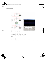
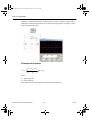
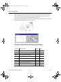
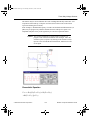
Documentation Conventions
When Multisim guides refer to a toolbar button, an image of the button appears in the left column.
Multisim guides use the convention Menu/Item to indicate menu commands. For example, “File/Open”
means choose the Open command from the File menu.
Multisim guides use the convention of an arrow () to indicate the start of procedural information.
Multisim guides use the construction CTRL-KEY and ALT-KEY to indicate when you need to hold down the
“Ctrl” or “Alt” key on your keyboard and press another key.
The Multisim Documentation Set
Multisim documentation consists of the User Guide, the Component Reference Guide and online help. All
Multisim users receive PDF versions of the User Guide and the Component Reference Guide.
You should also refer to Getting Started with NI Circuit Design Suite.
Component Reference Guide
This guide contains information on the components found in Multisim.
The chapters in the Component Reference Guide are organized to follow the component groups that are
found in the Multisim databases.
Online Help
Multisim offers a full helpfile system to support your use of the product.
Choose Help/Multisim Help to display the helpfile that explains the Multisim program in detail, or choose
Help/Component Reference to display the helpfile that contains details on the components families provided
with Multisim. Both are compiled HTML helpfiles, offering a table of contents and index.
In addition, you can display context-sensitive help by pressing F1 from any command or window, or by
clicking the Help button on any dialog box that offers it.
ComponentRef.book Page i Thursday, December 7, 2006 10:12 AM
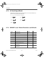
Table of Contents
1. Source Components
1.1
Ground . . . . . . . . . . . . . . . . . . . . . . . . . . . . . . . . . . . . . . . . . . . . . . . . . . . . . . . . . . . 1-1
1.2
Digital Ground . . . . . . . . . . . . . . . . . . . . . . . . . . . . . . . . . . . . . . . . . . . . . . . . . . . . . . 1-2
1.3
DC Voltage Source (Battery) . . . . . . . . . . . . . . . . . . . . . . . . . . . . . . . . . . . . . . . . . . . 1-2
1.4
Digital Power Supplies . . . . . . . . . . . . . . . . . . . . . . . . . . . . . . . . . . . . . . . . . . . . . . . 1-3
1.5
DC Current Source . . . . . . . . . . . . . . . . . . . . . . . . . . . . . . . . . . . . . . . . . . . . . . . . . . 1-4
1.6
AC Voltage Source . . . . . . . . . . . . . . . . . . . . . . . . . . . . . . . . . . . . . . . . . . . . . . . . . . 1-4
1.7
AC Current Source . . . . . . . . . . . . . . . . . . . . . . . . . . . . . . . . . . . . . . . . . . . . . . . . . . 1-5
1.8
Clock Source . . . . . . . . . . . . . . . . . . . . . . . . . . . . . . . . . . . . . . . . . . . . . . . . . . . . . . . 1-5
1.9
Amplitude Modulation (AM) Source . . . . . . . . . . . . . . . . . . . . . . . . . . . . . . . . . . . . . . 1-5
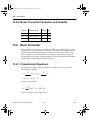
1.9.1
Characteristic Equation . . . . . . . . . . . . . . . . . . . . . . . . . . . . . . . . . . . . . . . . 1-6
1.10 FM Source . . . . . . . . . . . . . . . . . . . . . . . . . . . . . . . . . . . . . . . . . . . . . . . . . . . . . . . . .
1.10.1 FM Voltage Source. . . . . . . . . . . . . . . . . . . . . . . . . . . . . . . . . . . . . . . . . . . .
1.10.2 Characteristic Equation . . . . . . . . . . . . . . . . . . . . . . . . . . . . . . . . . . . . . . . .
1.10.3 FM Current Source . . . . . . . . . . . . . . . . . . . . . . . . . . . . . . . . . . . . . . . . . . . .
1.10.4 Characteristic Equation . . . . . . . . . . . . . . . . . . . . . . . . . . . . . . . . . . . . . . . .
1-6
1-6
1-6
1-7
1-7
1.11 FSK Source . . . . . . . . . . . . . . . . . . . . . . . . . . . . . . . . . . . . . . . . . . . . . . . . . . . . . . . . 1-7
1.12 Voltage-Controlled Voltage Source . . . . . . . . . . . . . . . . . . . . . . . . . . . . . . . . . . . . . . 1-8
1.13 Current-Controlled Voltage Source . . . . . . . . . . . . . . . . . . . . . . . . . . . . . . . . . . . . . . 1-9
1.14 Voltage-Controlled Current Source . . . . . . . . . . . . . . . . . . . . . . . . . . . . . . . . . . . . . . 1-9
1.15 Current-Controlled Current Source . . . . . . . . . . . . . . . . . . . . . . . . . . . . . . . . . . . . . . 1-9
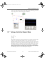
1.16 Voltage-Controlled Sine Wave . . . . . . . . . . . . . . . . . . . . . . . . . . . . . . . . . . . . . . . . 1-10
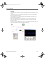
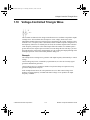
1.17 Voltage-Controlled Square Wave . . . . . . . . . . . . . . . . . . . . . . . . . . . . . . . . . . . . . . 1-11
1.18 Voltage-Controlled Triangle Wave . . . . . . . . . . . . . . . . . . . . . . . . . . . . . . . . . . . . . 1-13
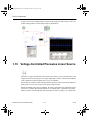
1.19 Voltage-Controlled Piecewise Linear Source . . . . . . . . . . . . . . . . . . . . . . . . . . . . . 1-14
National Instruments Corporation
i
Multisim Component Reference Guide
ComponentRef.book Page ii Thursday, December 7, 2006 10:12 AM
1.20 Piecewise Linear Source . . . . . . . . . . . . . . . . . . . . . . . . . . . . . . . . . . . . . . . . . . . . . 1-15
1.20.1 PWL Source Input Text File Specification. . . . . . . . . . . . . . . . . . . . . . . . . . 1-16
1.20.2 Piecewise Linear Voltage Source . . . . . . . . . . . . . . . . . . . . . . . . . . . . . . . . 1-17
1.20.3 Piecewise Linear Current Source . . . . . . . . . . . . . . . . . . . . . . . . . . . . . . . . 1-17
1.21 Pulse Source . . . . . . . . . . . . . . . . . . . . . . . . . . . . . . . . . . . . . . . . . . . . . . . . . . . . . . 1-18
1.21.1 Pulse Voltage Source . . . . . . . . . . . . . . . . . . . . . . . . . . . . . . . . . . . . . . . . . 1-19
1.21.2 Pulse Current Source . . . . . . . . . . . . . . . . . . . . . . . . . . . . . . . . . . . . . . . . . 1-19
1.22 Polynomial Source . . . . . . . . . . . . . . . . . . . . . . . . . . . . . . . . . . . . . . . . . . . . . . . . . . 1-19
1.23 Exponential Source . . . . . . . . . . . . . . . . . . . . . . . . . . . . . . . . . . . . . . . . . . . . . . . . . 1-20
1.23.1 Exponential Voltage Source . . . . . . . . . . . . . . . . . . . . . . . . . . . . . . . . . . . . 1-20
1.23.2 Exponential Current Source . . . . . . . . . . . . . . . . . . . . . . . . . . . . . . . . . . . . 1-21
1.24 Nonlinear Dependent Source . . . . . . . . . . . . . . . . . . . . . . . . . . . . . . . . . . . . . . . . . . 1-21
1.25 Controlled One-Shot . . . . . . . . . . . . . . . . . . . . . . . . . . . . . . . . . . . . . . . . . . . . . . . . 1-21
1.26 Magnetic Flux Source . . . . . . . . . . . . . . . . . . . . . . . . . . . . . . . . . . . . . . . . . . . . . . . . 1-22
1.27 Magnetic Flux Generator . . . . . . . . . . . . . . . . . . . . . . . . . . . . . . . . . . . . . . . . . . . . . 1-22
1.28 Multiplier . . . . . . . . . . . . . . . . . . . . . . . . . . . . . . . . . . . . . . . . . . . . . . . . . . . . . . . . . . 1-23
1.29 Divider . . . . . . . . . . . . . . . . . . . . . . . . . . . . . . . . . . . . . . . . . . . . . . . . . . . . . . . . . . . 1-25
1.30 Transfer Function Block . . . . . . . . . . . . . . . . . . . . . . . . . . . . . . . . . . . . . . . . . . . . . . 1-27
1.31 Voltage Gain Block . . . . . . . . . . . . . . . . . . . . . . . . . . . . . . . . . . . . . . . . . . . . . . . . . 1-29
1.32 Voltage Differentiator . . . . . . . . . . . . . . . . . . . . . . . . . . . . . . . . . . . . . . . . . . . . . . . . 1-31
1.32.1 Investigations . . . . . . . . . . . . . . . . . . . . . . . . . . . . . . . . . . . . . . . . . . . . . . . 1-32
1.33 Voltage Integrator . . . . . . . . . . . . . . . . . . . . . . . . . . . . . . . . . . . . . . . . . . . . . . . . . . 1-33
1.33.1 Investigations . . . . . . . . . . . . . . . . . . . . . . . . . . . . . . . . . . . . . . . . . . . . . . . 1-34
1.34 Voltage Hysteresis Block . . . . . . . . . . . . . . . . . . . . . . . . . . . . . . . . . . . . . . . . . . . . . 1-35
1.35 Voltage Limiter . . . . . . . . . . . . . . . . . . . . . . . . . . . . . . . . . . . . . . . . . . . . . . . . . . . . . 1-37
1.36 Current Limiter Block . . . . . . . . . . . . . . . . . . . . . . . . . . . . . . . . . . . . . . . . . . . . . . . . 1-38
1.37 Voltage-Controlled Limiter . . . . . . . . . . . . . . . . . . . . . . . . . . . . . . . . . . . . . . . . . . . . 1-41
1.38 Voltage Slew Rate Block . . . . . . . . . . . . . . . . . . . . . . . . . . . . . . . . . . . . . . . . . . . . . 1-43
1.39 Three-Way Voltage Summer . . . . . . . . . . . . . . . . . . . . . . . . . . . . . . . . . . . . . . . . . . 1-44
1.40 Three Phase Delta . . . . . . . . . . . . . . . . . . . . . . . . . . . . . . . . . . . . . . . . . . . . . . . . . . 1-46
1.41 Three Phase Wye . . . . . . . . . . . . . . . . . . . . . . . . . . . . . . . . . . . . . . . . . . . . . . . . . . 1-46
Multisim Component Reference Guide
ii
ni.com
ComponentRef.book Page iii Thursday, December 7, 2006 10:12 AM
1.42 Thermal Noise Source . . . . . . . . . . . . . . . . . . . . . . . . . . . . . . . . . . . . . . . . . . . . . . . 1-47
1.43 TDM Source . . . . . . . . . . . . . . . . . . . . . . . . . . . . . . . . . . . . . . . . . . . . . . . . . . . . . . 1-47
1.44 LVM Source . . . . . . . . . . . . . . . . . . . . . . . . . . . . . . . . . . . . . . . . . . . . . . . . . . . . . . . 1-48
1.45 ABM Sources . . . . . . . . . . . . . . . . . . . . . . . . . . . . . . . . . . . . . . . . . . . . . . . . . . . . . 1-49
1.46 Bipolar Sources . . . . . . . . . . . . . . . . . . . . . . . . . . . . . . . . . . . . . . . . . . . . . . . . . . . . 1-51
1.47 GAIN_2_PIN. . . . . . . . . . . . . . . . . . . . . . . . . . . . . . . . . . . . . . . . . . . . . . . . . . . . . . . 1-52
2. Basic Components
2.1
Connectors . . . . . . . . . . . . . . . . . . . . . . . . . . . . . . . . . . . . . . . . . . . . . . . . . . . . . . . . 2-1
2.2
Rated Virtual Components . . . . . . . . . . . . . . . . . . . . . . . . . . . . . . . . . . . . . . . . . . . . . 2-1
2.2.1
Rated 555 Timer . . . . . . . . . . . . . . . . . . . . . . . . . . . . . . . . . . . . . . . . . . . . . 2-2
2.2.2
Rated BJTs . . . . . . . . . . . . . . . . . . . . . . . . . . . . . . . . . . . . . . . . . . . . . . . . . 2-3
2.2.3
Rated Capacitors . . . . . . . . . . . . . . . . . . . . . . . . . . . . . . . . . . . . . . . . . . . . . 2-4
2.2.4
Rated Diodes . . . . . . . . . . . . . . . . . . . . . . . . . . . . . . . . . . . . . . . . . . . . . . . . 2-4
2.2.5
Rated Fuses . . . . . . . . . . . . . . . . . . . . . . . . . . . . . . . . . . . . . . . . . . . . . . . . . 2-5
2.2.6
Rated Inductors . . . . . . . . . . . . . . . . . . . . . . . . . . . . . . . . . . . . . . . . . . . . . . 2-6
2.2.7
Rated LEDs . . . . . . . . . . . . . . . . . . . . . . . . . . . . . . . . . . . . . . . . . . . . . . . . . 2-6
2.2.8
Rated DC Motor . . . . . . . . . . . . . . . . . . . . . . . . . . . . . . . . . . . . . . . . . . . . . . 2-7
2.2.9
Rated Relay . . . . . . . . . . . . . . . . . . . . . . . . . . . . . . . . . . . . . . . . . . . . . . . . . 2-8
2.2.10 Rated Opamp . . . . . . . . . . . . . . . . . . . . . . . . . . . . . . . . . . . . . . . . . . . . . . . . 2-9
2.2.11 Rated Photodiode. . . . . . . . . . . . . . . . . . . . . . . . . . . . . . . . . . . . . . . . . . . . 2-10
2.2.12 Rated Phototransistor. . . . . . . . . . . . . . . . . . . . . . . . . . . . . . . . . . . . . . . . . 2-10
2.2.13 Rated Potentiometer . . . . . . . . . . . . . . . . . . . . . . . . . . . . . . . . . . . . . . . . . 2-11
2.2.14 Rated Pullup . . . . . . . . . . . . . . . . . . . . . . . . . . . . . . . . . . . . . . . . . . . . . . . . 2-12
2.2.15 Rated Resistor . . . . . . . . . . . . . . . . . . . . . . . . . . . . . . . . . . . . . . . . . . . . . . 2-12
2.2.16 Rated Transformers . . . . . . . . . . . . . . . . . . . . . . . . . . . . . . . . . . . . . . . . . . 2-13
2.2.17 Rated Variable Capacitor . . . . . . . . . . . . . . . . . . . . . . . . . . . . . . . . . . . . . . 2-14
2.2.18 Rated Variable Inductor . . . . . . . . . . . . . . . . . . . . . . . . . . . . . . . . . . . . . . . 2-15
2.2.19 Rated Virtual Components Toolbar . . . . . . . . . . . . . . . . . . . . . . . . . . . . . . 2-16
2.3
Sockets. . . . . . . . . . . . . . . . . . . . . . . . . . . . . . . . . . . . . . . . . . . . . . . . . . . . . . . . . . . 2-16
2.4
Switch . . . . . . . . . . . . . . . . . . . . . . . . . . . . . . . . . . . . . . . . . . . . . . . . . . . . . . . . . . . 2-16
2.4.1
Switch Packs . . . . . . . . . . . . . . . . . . . . . . . . . . . . . . . . . . . . . . . . . . . . . . . 2-17
2.5
SBREAK . . . . . . . . . . . . . . . . . . . . . . . . . . . . . . . . . . . . . . . . . . . . . . . . . . . . . . . . . 2-18
National Instruments Corporation
iii
Multisim Component Reference Guide
ComponentRef.book Page iv Thursday, December 7, 2006 10:12 AM
2.6
Resistor . . . . . . . . . . . . . . . . . . . . . . . . . . . . . . . . . . . . . . . . . . . . . . . . . . . . . . . . . . 2-18
2.6.1
About Resistance . . . . . . . . . . . . . . . . . . . . . . . . . . . . . . . . . . . . . . . . . . . . 2-19
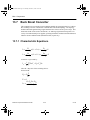
2.6.2
Characteristic Equation . . . . . . . . . . . . . . . . . . . . . . . . . . . . . . . . . . . . . . . . 2-19
2.6.3
Changing a Placed Resistor’s Value. . . . . . . . . . . . . . . . . . . . . . . . . . . . . . 2-19
2.7
Capacitor . . . . . . . . . . . . . . . . . . . . . . . . . . . . . . . . . . . . . . . . . . . . . . . . . . . . . . . . . 2-20
2.7.1
Characteristic Equation . . . . . . . . . . . . . . . . . . . . . . . . . . . . . . . . . . . . . . . . 2-21
2.7.2
DC Model . . . . . . . . . . . . . . . . . . . . . . . . . . . . . . . . . . . . . . . . . . . . . . . . . . 2-21
2.7.3
Time-Domain Model . . . . . . . . . . . . . . . . . . . . . . . . . . . . . . . . . . . . . . . . . . 2-21
2.7.4
AC Frequency Model . . . . . . . . . . . . . . . . . . . . . . . . . . . . . . . . . . . . . . . . . 2-22
2.7.5
Changing a Placed Capacitor’s Value. . . . . . . . . . . . . . . . . . . . . . . . . . . . . 2-22
2.8
Inductor . . . . . . . . . . . . . . . . . . . . . . . . . . . . . . . . . . . . . . . . . . . . . . . . . . . . . . . . . . 2-23
2.8.1
Characteristic Equation . . . . . . . . . . . . . . . . . . . . . . . . . . . . . . . . . . . . . . . . 2-23
2.8.2
DC Model . . . . . . . . . . . . . . . . . . . . . . . . . . . . . . . . . . . . . . . . . . . . . . . . . . 2-23
2.8.3
Time-Domain Model . . . . . . . . . . . . . . . . . . . . . . . . . . . . . . . . . . . . . . . . . . 2-23
2.8.4
AC Frequency Model . . . . . . . . . . . . . . . . . . . . . . . . . . . . . . . . . . . . . . . . . 2-24
2.8.5
Changing a Placed Inductor’s Value . . . . . . . . . . . . . . . . . . . . . . . . . . . . . . 2-25
2.9
Advanced Inductor . . . . . . . . . . . . . . . . . . . . . . . . . . . . . . . . . . . . . . . . . . . . . . . . . . 2-25
2.9.1
Advanced Inductor Model Implementation . . . . . . . . . . . . . . . . . . . . . . . . . 2-28
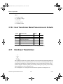
2.10 Transformer . . . . . . . . . . . . . . . . . . . . . . . . . . . . . . . . . . . . . . . . . . . . . . . . . . . . . . . 2-29
2.10.1 Characteristic Equation . . . . . . . . . . . . . . . . . . . . . . . . . . . . . . . . . . . . . . . . 2-29
2.10.2 Ideal Transformer Model Parameters and Defaults . . . . . . . . . . . . . . . . . . 2-30
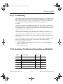
2.11 Nonlinear Transformer . . . . . . . . . . . . . . . . . . . . . . . . . . . . . . . . . . . . . . . . . . . . . . . 2-30
2.11.1 Customizing . . . . . . . . . . . . . . . . . . . . . . . . . . . . . . . . . . . . . . . . . . . . . . . . 2-31
2.11.2 Nonlinear Transformer Parameters and Defaults . . . . . . . . . . . . . . . . . . . . 2-31
2.12 Relay . . . . . . . . . . . . . . . . . . . . . . . . . . . . . . . . . . . . . . . . . . . . . . . . . . . . . . . . . . . . 2-32
2.12.1 Model . . . . . . . . . . . . . . . . . . . . . . . . . . . . . . . . . . . . . . . . . . . . . . . . . . . . . 2-33
2.12.2 Characteristic Equation . . . . . . . . . . . . . . . . . . . . . . . . . . . . . . . . . . . . . . . . 2-33
2.13 Variable Capacitor . . . . . . . . . . . . . . . . . . . . . . . . . . . . . . . . . . . . . . . . . . . . . . . . . . 2-33
2.14 Variable Inductor . . . . . . . . . . . . . . . . . . . . . . . . . . . . . . . . . . . . . . . . . . . . . . . . . . . 2-35
2.15 Potentiometer . . . . . . . . . . . . . . . . . . . . . . . . . . . . . . . . . . . . . . . . . . . . . . . . . . . . . . 2-36
2.16 Pullup . . . . . . . . . . . . . . . . . . . . . . . . . . . . . . . . . . . . . . . . . . . . . . . . . . . . . . . . . . . . 2-37
2.17 Resistor Packs . . . . . . . . . . . . . . . . . . . . . . . . . . . . . . . . . . . . . . . . . . . . . . . . . . . . . 2-38
2.18 Voltage Controlled Resistor . . . . . . . . . . . . . . . . . . . . . . . . . . . . . . . . . . . . . . . . . . . 2-38
2.19 Voltage Controlled Capacitor . . . . . . . . . . . . . . . . . . . . . . . . . . . . . . . . . . . . . . . . . . 2-38
2.20 Voltage Controlled Inductor . . . . . . . . . . . . . . . . . . . . . . . . . . . . . . . . . . . . . . . . . . . 2-38
Multisim Component Reference Guide
iv
ni.com
ComponentRef.book Page v Thursday, December 7, 2006 10:12 AM
2.21 Magnetic Core . . . . . . . . . . . . . . . . . . . . . . . . . . . . . . . . . . . . . . . . . . . . . . . . . . . . . 2-39
2.22 Coreless Coil . . . . . . . . . . . . . . . . . . . . . . . . . . . . . . . . . . . . . . . . . . . . . . . . . . . . . . 2-40
2.22.1 Characteristic Equation . . . . . . . . . . . . . . . . . . . . . . . . . . . . . . . . . . . . . . . 2-41
2.22.2 Coreless Coil Parameters and Defaults . . . . . . . . . . . . . . . . . . . . . . . . . . . 2-41
2.23 Z Loads . . . . . . . . . . . . . . . . . . . . . . . . . . . . . . . . . . . . . . . . . . . . . . . . . . . . . . . . . .
2.23.1 A+jB Block . . . . . . . . . . . . . . . . . . . . . . . . . . . . . . . . . . . . . . . . . . . . . . . . .
2.23.2 A-jB Block . . . . . . . . . . . . . . . . . . . . . . . . . . . . . . . . . . . . . . . . . . . . . . . . . .
2.23.3 Z Load 1 . . . . . . . . . . . . . . . . . . . . . . . . . . . . . . . . . . . . . . . . . . . . . . . . . . .
2.23.4 Z Load 1 Delta . . . . . . . . . . . . . . . . . . . . . . . . . . . . . . . . . . . . . . . . . . . . . .
2.23.5 Z Load 1 Wye . . . . . . . . . . . . . . . . . . . . . . . . . . . . . . . . . . . . . . . . . . . . . . .
2.23.6 Z Load 2 . . . . . . . . . . . . . . . . . . . . . . . . . . . . . . . . . . . . . . . . . . . . . . . . . . .
2.23.7 Z Load 2 Delta . . . . . . . . . . . . . . . . . . . . . . . . . . . . . . . . . . . . . . . . . . . . . .
2.23.8 Z Load 2 Wye . . . . . . . . . . . . . . . . . . . . . . . . . . . . . . . . . . . . . . . . . . . . . . .
2.23.9 Z Load 3 . . . . . . . . . . . . . . . . . . . . . . . . . . . . . . . . . . . . . . . . . . . . . . . . . . .
2-41
2-41
2-42
2-42
2-42
2-43
2-43
2-43
2-44
2-44
3. Diodes
3.1
Diode . . . . . . . . . . . . . . . . . . . . . . . . . . . . . . . . . . . . . . . . . . . . . . . . . . . . . . . . . . . . .
3.1.1
Diodes: Background Information . . . . . . . . . . . . . . . . . . . . . . . . . . . . . . . . .
3.1.2
DC Model . . . . . . . . . . . . . . . . . . . . . . . . . . . . . . . . . . . . . . . . . . . . . . . . . . .
3.1.3
Time-Domain Model . . . . . . . . . . . . . . . . . . . . . . . . . . . . . . . . . . . . . . . . . . .
3.1.4
AC Small-Signal Model . . . . . . . . . . . . . . . . . . . . . . . . . . . . . . . . . . . . . . . .
3.1.5
Diode Parameters and Defaults . . . . . . . . . . . . . . . . . . . . . . . . . . . . . . . . . .
3.2
Pin Diode . . . . . . . . . . . . . . . . . . . . . . . . . . . . . . . . . . . . . . . . . . . . . . . . . . . . . . . . . . 3-5
3.3
Zener Diode . . . . . . . . . . . . . . . . . . . . . . . . . . . . . . . . . . . . . . . . . . . . . . . . . . . . . . . . 3-6
3.3.1
DC Model . . . . . . . . . . . . . . . . . . . . . . . . . . . . . . . . . . . . . . . . . . . . . . . . . . . 3-6
3.3.2
Zener Diode Parameters and Defaults . . . . . . . . . . . . . . . . . . . . . . . . . . . . . 3-7
3.4
LED (Light-Emitting Diode) . . . . . . . . . . . . . . . . . . . . . . . . . . . . . . . . . . . . . . . . . . . . 3-8
3.4.1
Background Information . . . . . . . . . . . . . . . . . . . . . . . . . . . . . . . . . . . . . . . . 3-8
3.4.2
LED Parameters and Defaults . . . . . . . . . . . . . . . . . . . . . . . . . . . . . . . . . . . 3-9
3.5
Bar LED . . . . . . . . . . . . . . . . . . . . . . . . . . . . . . . . . . . . . . . . . . . . . . . . . . . . . . . . . . . 3-9
3.6
Full-Wave Bridge Rectifier . . . . . . . . . . . . . . . . . . . . . . . . . . . . . . . . . . . . . . . . . . . .
3.6.1
Characteristic Equation . . . . . . . . . . . . . . . . . . . . . . . . . . . . . . . . . . . . . . .
3.6.2
Model . . . . . . . . . . . . . . . . . . . . . . . . . . . . . . . . . . . . . . . . . . . . . . . . . . . . .
3.6.3
Full-Wave Bridge Rectifier Parameters and Defaults . . . . . . . . . . . . . . . . .
3.7
Schottky Diode . . . . . . . . . . . . . . . . . . . . . . . . . . . . . . . . . . . . . . . . . . . . . . . . . . . . 3-12
National Instruments Corporation
v
3-1
3-1
3-2
3-3
3-4
3-4
3-10
3-10
3-10
3-11
Multisim Component Reference Guide
ComponentRef.book Page vi Thursday, December 7, 2006 10:12 AM
3.8
Silicon-Controlled Rectifier . . . . . . . . . . . . . . . . . . . . . . . . . . . . . . . . . . . . . . . . . . . . 3-12
3.8.1
Model . . . . . . . . . . . . . . . . . . . . . . . . . . . . . . . . . . . . . . . . . . . . . . . . . . . . . 3-13
3.8.2
Time-Domain Model . . . . . . . . . . . . . . . . . . . . . . . . . . . . . . . . . . . . . . . . . . 3-13
3.8.3
AC Small-Signal Model . . . . . . . . . . . . . . . . . . . . . . . . . . . . . . . . . . . . . . . . 3-14
3.8.4
SCR Parameters and Defaults . . . . . . . . . . . . . . . . . . . . . . . . . . . . . . . . . . 3-14
3.9
DIAC . . . . . . . . . . . . . . . . . . . . . . . . . . . . . . . . . . . . . . . . . . . . . . . . . . . . . . . . . . . . 3-14
3.9.1
DC Model . . . . . . . . . . . . . . . . . . . . . . . . . . . . . . . . . . . . . . . . . . . . . . . . . . 3-15
3.9.2
Time-Domain and AC Small-Signal Models . . . . . . . . . . . . . . . . . . . . . . . . 3-15
3.9.3
DIAC Parameters and Defaults. . . . . . . . . . . . . . . . . . . . . . . . . . . . . . . . . . 3-16
3.10 TRIAC . . . . . . . . . . . . . . . . . . . . . . . . . . . . . . . . . . . . . . . . . . . . . . . . . . . . . . . . . . . 3-16
3.10.1 Model . . . . . . . . . . . . . . . . . . . . . . . . . . . . . . . . . . . . . . . . . . . . . . . . . . . . . 3-16
3.11 Varactor Diode . . . . . . . . . . . . . . . . . . . . . . . . . . . . . . . . . . . . . . . . . . . . . . . . . . . . . 3-18
4. Transistors
4.1
BJT (NPN & PNP) . . . . . . . . . . . . . . . . . . . . . . . . . . . . . . . . . . . . . . . . . . . . . . . . . . . 4-1
4.1.1
Characteristic Equations . . . . . . . . . . . . . . . . . . . . . . . . . . . . . . . . . . . . . . . . 4-2
4.1.2
Time-Domain Model . . . . . . . . . . . . . . . . . . . . . . . . . . . . . . . . . . . . . . . . . . . 4-3
4.1.3
AC Small-Signal Model . . . . . . . . . . . . . . . . . . . . . . . . . . . . . . . . . . . . . . . . . 4-5
4.1.4
BJT Model Parameters and Defaults . . . . . . . . . . . . . . . . . . . . . . . . . . . . . . 4-6
4.2
Resistor Biased BJT (NPN & PNP) . . . . . . . . . . . . . . . . . . . . . . . . . . . . . . . . . . . . . . 4-8
4.3
Darlington Transistor (NPN & PNP) . . . . . . . . . . . . . . . . . . . . . . . . . . . . . . . . . . . . . . 4-8
4.3.1
DC Bias Model . . . . . . . . . . . . . . . . . . . . . . . . . . . . . . . . . . . . . . . . . . . . . . . 4-9
4.3.2
AC Model . . . . . . . . . . . . . . . . . . . . . . . . . . . . . . . . . . . . . . . . . . . . . . . . . . . 4-9
4.3.2.1
AC Input Impedance . . . . . . . . . . . . . . . . . . . . . . . . . . . . . . . . . . 4-9
4.3.2.2 AC Current Gain . . . . . . . . . . . . . . . . . . . . . . . . . . . . . . . . . . . . . 4-10
4.4
BJT Array . . . . . . . . . . . . . . . . . . . . . . . . . . . . . . . . . . . . . . . . . . . . . . . . . . . . . . . . . 4-10
4.4.1
General-purpose PNP Transistor Array . . . . . . . . . . . . . . . . . . . . . . . . . . . 4-10
4.4.2
NPN/PNP Transistor Array . . . . . . . . . . . . . . . . . . . . . . . . . . . . . . . . . . . . . 4-10
4.4.3
General-purpose High-current NPN Transistor Array . . . . . . . . . . . . . . . . . 4-11
4.5
P-Channel MOSFET . . . . . . . . . . . . . . . . . . . . . . . . . . . . . . . . . . . . . . . . . . . . . . . . . 4-11
4.6
N-Channel MOSFET . . . . . . . . . . . . . . . . . . . . . . . . . . . . . . . . . . . . . . . . . . . . . . . . 4-11
4.7
MOSFET . . . . . . . . . . . . . . . . . . . . . . . . . . . . . . . . . . . . . . . . . . . . . . . . . . . . . . . . . 4-11
4.7.1
Depletion MOSFETs . . . . . . . . . . . . . . . . . . . . . . . . . . . . . . . . . . . . . . . . . . 4-12
4.7.2
Enhancement MOSFETs . . . . . . . . . . . . . . . . . . . . . . . . . . . . . . . . . . . . . . 4-12
4.7.3
DC Model . . . . . . . . . . . . . . . . . . . . . . . . . . . . . . . . . . . . . . . . . . . . . . . . . . 4-12
4.7.4
Time-Domain Model . . . . . . . . . . . . . . . . . . . . . . . . . . . . . . . . . . . . . . . . . . 4-13
Multisim Component Reference Guide
vi
ni.com
ComponentRef.book Page vii Thursday, December 7, 2006 10:12 AM
4.7.5
4.7.6
AC Small-Signal Model . . . . . . . . . . . . . . . . . . . . . . . . . . . . . . . . . . . . . . . 4-14
MOSFET Level 1 Model Parameters and Defaults . . . . . . . . . . . . . . . . . . 4-14
4.8
MOSFET Thermal Model . . . . . . . . . . . . . . . . . . . . . . . . . . . . . . . . . . . . . . . . . . . . . 4-16
4.9
JFETs (Junction FETs) . . . . . . . . . . . . . . . . . . . . . . . . . . . . . . . . . . . . . . . . . . . . . . 4-17
4.9.1
DC Model . . . . . . . . . . . . . . . . . . . . . . . . . . . . . . . . . . . . . . . . . . . . . . . . . . 4-17
4.9.2
JFET Model Parameters and Defaults . . . . . . . . . . . . . . . . . . . . . . . . . . . . 4-19
4.10 Power MOSFET (N/P) . . . . . . . . . . . . . . . . . . . . . . . . . . . . . . . . . . . . . . . . . . . . . . . 4-20
4.11 Power MOSFET Complementary. . . . . . . . . . . . . . . . . . . . . . . . . . . . . . . . . . . . . . . 4-20
4.12 N-Channel & P-Channel GaAsFET . . . . . . . . . . . . . . . . . . . . . . . . . . . . . . . . . . . . . 4-21
4.12.1 Model and Characteristic Equations. . . . . . . . . . . . . . . . . . . . . . . . . . . . . . 4-21
4.12.2 GaAsFET Parameters and Defaults . . . . . . . . . . . . . . . . . . . . . . . . . . . . . . 4-22
4.13 IGBT . . . . . . . . . . . . . . . . . . . . . . . . . . . . . . . . . . . . . . . . . . . . . . . . . . . . . . . . . . . . 4-22
4.14 Unijunction Transistors. . . . . . . . . . . . . . . . . . . . . . . . . . . . . . . . . . . . . . . . . . . . . . . 4-23
5. Analog Components
5.1
Opamp
5.1.1
5.1.2
5.1.3
............................................................
Ideal Opamp Model . . . . . . . . . . . . . . . . . . . . . . . . . . . . . . . . . . . . . . . . . . .
Opamp: Background Information . . . . . . . . . . . . . . . . . . . . . . . . . . . . . . . . .
Opamp: Simulation Models . . . . . . . . . . . . . . . . . . . . . . . . . . . . . . . . . . . . .
5.1.3.1 Virtual 3-Terminal Opamp . . . . . . . . . . . . . . . . . . . . . . . . . . . . . .
5.1.3.2 Virtual 5-Terminal Opamp . . . . . . . . . . . . . . . . . . . . . . . . . . . . . .
5.1.3.3 Real Models . . . . . . . . . . . . . . . . . . . . . . . . . . . . . . . . . . . . . . . . .
5.2
Norton Opamp . . . . . . . . . . . . . . . . . . . . . . . . . . . . . . . . . . . . . . . . . . . . . . . . . . . . . . 5-8
5.3
Comparator . . . . . . . . . . . . . . . . . . . . . . . . . . . . . . . . . . . . . . . . . . . . . . . . . . . . . . . 5-9
5.3.1
Comparator: Simulation models . . . . . . . . . . . . . . . . . . . . . . . . . . . . . . . . . 5-10
5.4
Wide Band Amplifier . . . . . . . . . . . . . . . . . . . . . . . . . . . . . . . . . . . . . . . . . . . . . . . . 5-10
5.4.1
Wide Band Amplifier: Simulation models . . . . . . . . . . . . . . . . . . . . . . . . . . 5-10
5.5
Special Function. . . . . . . . . . . . . . . . . . . . . . . . . . . . . . . . . . . . . . . . . . . . . . . . . . . . 5-11
5.5.1
Special Function: Simulation models . . . . . . . . . . . . . . . . . . . . . . . . . . . . . 5-11
National Instruments Corporation
vii
5-1
5-1
5-2
5-3
5-3
5-5
5-8
Multisim Component Reference Guide
ComponentRef.book Page viii Thursday, December 7, 2006 10:12 AM
6. TTL
6.1
Standard TTL . . . . . . . . . . . . . . . . . . . . . . . . . . . . . . . . . . . . . . . . . . . . . . . . . . . . . . . 6-1
6.2
Schottky TTL . . . . . . . . . . . . . . . . . . . . . . . . . . . . . . . . . . . . . . . . . . . . . . . . . . . . . . . . 6-1
6.3
Low-Power Schottky TTL . . . . . . . . . . . . . . . . . . . . . . . . . . . . . . . . . . . . . . . . . . . . . . 6-2
6.4
74xx . . . . . . . . . . . . . . . . . . . . . . . . . . . . . . . . . . . . . . . . . . . . . . . . . . . . . . . . . . . . . . 6-2
6.4.1
74xx00 (Quad 2-In NAND) . . . . . . . . . . . . . . . . . . . . . . . . . . . . . . . . . . . . . . 6-2
6.4.2
74xx01 (Quad 2-In NAND) . . . . . . . . . . . . . . . . . . . . . . . . . . . . . . . . . . . . . . 6-3
6.4.3
74xx02 (Quad 2-In NOR) . . . . . . . . . . . . . . . . . . . . . . . . . . . . . . . . . . . . . . . 6-3
6.4.4
74xx03 (Quad 2-In NAND (Ls-OC)) . . . . . . . . . . . . . . . . . . . . . . . . . . . . . . . 6-3
6.4.5
74xx04 (Hex INVERTER) . . . . . . . . . . . . . . . . . . . . . . . . . . . . . . . . . . . . . . . 6-4
6.4.6
74xx05 (Hex INVERTER (OC)) . . . . . . . . . . . . . . . . . . . . . . . . . . . . . . . . . . 6-4
6.4.7
74xx06 (Hex INVERTER (OC)) . . . . . . . . . . . . . . . . . . . . . . . . . . . . . . . . . . 6-5
6.4.8
74xx07 (Hex BUFFER (OC)) . . . . . . . . . . . . . . . . . . . . . . . . . . . . . . . . . . . . 6-5
6.4.9
74xx08 (Quad 2-In AND) . . . . . . . . . . . . . . . . . . . . . . . . . . . . . . . . . . . . . . . 6-5
6.4.10 74xx09 (Quad 2-In AND (OC)) . . . . . . . . . . . . . . . . . . . . . . . . . . . . . . . . . . . 6-6
6.4.11 74xx10 (Tri 3-In NAND) . . . . . . . . . . . . . . . . . . . . . . . . . . . . . . . . . . . . . . . . 6-6
6.4.12 74xx100 (8-Bit Bist Latch) . . . . . . . . . . . . . . . . . . . . . . . . . . . . . . . . . . . . . . 6-7
6.4.13 74xx107 (Dual JK FF(clr)) . . . . . . . . . . . . . . . . . . . . . . . . . . . . . . . . . . . . . . 6-7
6.4.14 74xx109 (Dual JK FF (+edge, pre, clr)) . . . . . . . . . . . . . . . . . . . . . . . . . . . . 6-8
6.4.15 74xx11 (Tri 3-In AND) . . . . . . . . . . . . . . . . . . . . . . . . . . . . . . . . . . . . . . . . . 6-8
6.4.16 74xx112 (Dual JK FF(-edge, pre, clr)) . . . . . . . . . . . . . . . . . . . . . . . . . . . . . 6-9
6.4.17 74xx113 (Dual JK MS-SLV FF (-edge, pre)) . . . . . . . . . . . . . . . . . . . . . . . . 6-9
6.4.18 74xx114 (Dual JK FF (-edge, pre, com clk & clr)) . . . . . . . . . . . . . . . . . . . 6-10
6.4.19 74xx116 (Dual 4-bit latches (clr)) . . . . . . . . . . . . . . . . . . . . . . . . . . . . . . . . 6-10
6.4.20 74xx12 (Tri 3-In NAND (OC)) . . . . . . . . . . . . . . . . . . . . . . . . . . . . . . . . . . . 6-11
6.4.21 74xx125 (Quad bus BUFFER w/3-state Out) . . . . . . . . . . . . . . . . . . . . . . . 6-11
6.4.22 74xx126 (Quad bus BUFFER w/3-state Out) . . . . . . . . . . . . . . . . . . . . . . . 6-12
6.4.23 74xx13 (Dual 4-In NAND (Schmitt)) . . . . . . . . . . . . . . . . . . . . . . . . . . . . . . 6-12
6.4.24 74xx132 (Quad 2-In NAND (Schmitt)) . . . . . . . . . . . . . . . . . . . . . . . . . . . . 6-12
6.4.25 74xx133 (13-In NAND) . . . . . . . . . . . . . . . . . . . . . . . . . . . . . . . . . . . . . . . . 6-12
6.4.26 74xx134 (12-In NAND w/3-state Out) . . . . . . . . . . . . . . . . . . . . . . . . . . . . 6-13
6.4.27 74xx135 (Quad Ex-OR/NOR Gate) . . . . . . . . . . . . . . . . . . . . . . . . . . . . . . 6-13
6.4.28 74xx136 (Quad 2-in Exc-OR gate) . . . . . . . . . . . . . . . . . . . . . . . . . . . . . . . 6-14
6.4.29 74xx138 (3-to-8 Dec) . . . . . . . . . . . . . . . . . . . . . . . . . . . . . . . . . . . . . . . . . 6-14
6.4.30 74xx139 (Dual 2-to-4 Dec/DEMUX) . . . . . . . . . . . . . . . . . . . . . . . . . . . . . . 6-15
6.4.31 74xx14 (Hex INVERTER (Schmitt)) . . . . . . . . . . . . . . . . . . . . . . . . . . . . . . 6-15
6.4.32 74xx145 (BCD-to-Decimal Dec) . . . . . . . . . . . . . . . . . . . . . . . . . . . . . . . . . 6-15
6.4.33 74xx147 (10-to-4 Priority Enc) . . . . . . . . . . . . . . . . . . . . . . . . . . . . . . . . . . 6-16
6.4.34 74xx148 (8-to-3 Priority Enc) . . . . . . . . . . . . . . . . . . . . . . . . . . . . . . . . . . . 6-17
Multisim Component Reference Guide
viii
ni.com
ComponentRef.book Page ix Thursday, December 7, 2006 10:12 AM
6.4.35
6.4.36
6.4.37
6.4.38
6.4.39
6.4.40
6.4.41
6.4.42
6.4.43
6.4.44
6.4.45
6.4.46
6.4.47
6.4.48
6.4.49
6.4.50
6.4.51
6.4.52
6.4.53
6.4.54
6.4.55
6.4.56
6.4.57
6.4.58
6.4.59
6.4.60
6.4.61
6.4.62
6.4.63
6.4.64
6.4.65
6.4.66
6.4.67
6.4.68
6.4.69
6.4.70
6.4.71
6.4.72
6.4.73
6.4.74
6.4.75
6.4.76
74xx15 (3 3-Input AND) . . . . . . . . . . . . . . . . . . . . . . . . . . . . . . . . . . . . . . .
74xx150 (1-of-16 Data Sel/MUX) . . . . . . . . . . . . . . . . . . . . . . . . . . . . . . .
74xx151 (1-of-8 Data Sel/MUX) . . . . . . . . . . . . . . . . . . . . . . . . . . . . . . . .
74xx152 (Data Sel/MUX) . . . . . . . . . . . . . . . . . . . . . . . . . . . . . . . . . . . . . .
74xx153 (Dual 4-to-1 Data Sel/MUX) . . . . . . . . . . . . . . . . . . . . . . . . . . . .
74xx154 (4-to-16 Dec/DEMUX) . . . . . . . . . . . . . . . . . . . . . . . . . . . . . . . . .
74xx155 (Dual 2-to-4 Dec/DEMUX) . . . . . . . . . . . . . . . . . . . . . . . . . . . . .
74xx156 (Dual 2-to-4 Dec/DEMUX (OC)) . . . . . . . . . . . . . . . . . . . . . . . . .
74xx157 (Quad 2-to-1 Data Sel/MUX) . . . . . . . . . . . . . . . . . . . . . . . . . . .
74xx158 (Quad 2-to-1 Data Sel/MUX) . . . . . . . . . . . . . . . . . . . . . . . . . . .
74xx159 (4-to-16 Dec/DEMUX (OC)) . . . . . . . . . . . . . . . . . . . . . . . . . . . .
74xx16 (Hex INVERTER (OC)) . . . . . . . . . . . . . . . . . . . . . . . . . . . . . . . . .
74xx160 (Sync 4-bit Decade Counter (clr)) . . . . . . . . . . . . . . . . . . . . . . . .
74xx161 (Sync 4-bit Bin Counter) . . . . . . . . . . . . . . . . . . . . . . . . . . . . . . .
74xx162 (Sync 4-bit Decade Counter) . . . . . . . . . . . . . . . . . . . . . . . . . . .
74xx163 (Sync 4-bit Binary Counter) . . . . . . . . . . . . . . . . . . . . . . . . . . . .
74xx164 (8-bit Parallel-Out Serial Shift Reg) . . . . . . . . . . . . . . . . . . . . . .
74xx165 (Parallel-load 8-bit Shift Reg) . . . . . . . . . . . . . . . . . . . . . . . . . . .
74xx166 (Parallel-load 8-bit Shift Reg) . . . . . . . . . . . . . . . . . . . . . . . . . . .
74xx169 (Sync 4-bit up/down Binary Counter) . . . . . . . . . . . . . . . . . . . . .
74xx17 (Hex BUFFER (OC)) . . . . . . . . . . . . . . . . . . . . . . . . . . . . . . . . . . .
74xx173 (4-bit D-type Reg w/3-state Out) . . . . . . . . . . . . . . . . . . . . . . . . .
74xx174 (Hex D-type FF (clr)) . . . . . . . . . . . . . . . . . . . . . . . . . . . . . . . . . .
74xx175 (Quad D-type FF (clr)) . . . . . . . . . . . . . . . . . . . . . . . . . . . . . . . .
74xx180 (9-bit Odd/even Par GEN) . . . . . . . . . . . . . . . . . . . . . . . . . . . . .
74xx181 (Alu/Function Generator) . . . . . . . . . . . . . . . . . . . . . . . . . . . . . .
74xx182 (Look-ahead Carry GEN) . . . . . . . . . . . . . . . . . . . . . . . . . . . . . .
74xx190 (Sync BCD up/down Counter) . . . . . . . . . . . . . . . . . . . . . . . . . .
74xx191 (Sync 4-bit up/down Counter) . . . . . . . . . . . . . . . . . . . . . . . . . . .
74xx192 (Sync BCD Up/down Counter) . . . . . . . . . . . . . . . . . . . . . . . . . .
74xx193 (Sync 4-bit Bin Up/down Counter) . . . . . . . . . . . . . . . . . . . . . . .
74xx194 (4-bit Bidirect Univ. Shift Reg) . . . . . . . . . . . . . . . . . . . . . . . . . .
74xx195 (4-bit Parallel-Access Shift Reg) . . . . . . . . . . . . . . . . . . . . . . . . .
74xx198 (8-bit Shift Reg (shl/shr ctrl)) . . . . . . . . . . . . . . . . . . . . . . . . . . . .
74xx199 (8-bit Shift Reg (sh/ld ctrl)) . . . . . . . . . . . . . . . . . . . . . . . . . . . . .
74xx20 (Dual 4-In NAND) . . . . . . . . . . . . . . . . . . . . . . . . . . . . . . . . . . . . .
74xx21 (Dual 4-In AND) . . . . . . . . . . . . . . . . . . . . . . . . . . . . . . . . . . . . . .
74xx22 (Dual 4-In NAND (OC)) . . . . . . . . . . . . . . . . . . . . . . . . . . . . . . . . .
74xx238 (3-to-8 line Dec/DEMUX) . . . . . . . . . . . . . . . . . . . . . . . . . . . . . . .
74xx24 (Dual 4-input NAND Schmitt) . . . . . . . . . . . . . . . . . . . . . . . . . . . . .
74xx240 (Octal BUFFER w/3-state Out) . . . . . . . . . . . . . . . . . . . . . . . . . .
74xx241 (Octal BUFFER w/3-state Out) . . . . . . . . . . . . . . . . . . . . . . . . . .
National Instruments Corporation
ix
6-17
6-17
6-18
6-19
6-19
6-20
6-21
6-21
6-21
6-22
6-22
6-23
6-24
6-24
6-25
6-26
6-27
6-27
6-28
6-28
6-29
6-29
6-30
6-30
6-30
6-31
6-32
6-34
6-35
6-35
6-36
6-37
6-37
6-38
6-39
6-40
6-40
6-41
6-41
6-42
6-42
6-42
Multisim Component Reference Guide
ComponentRef.book Page x Thursday, December 7, 2006 10:12 AM
6.4.77
6.4.78
6.4.79
6.4.80
6.4.81
6.4.82
6.4.83
6.4.84
6.4.85
6.4.86
6.4.87
6.4.88
6.4.89
6.4.90
6.4.91
6.4.92
6.4.93
6.4.94
6.4.95
6.4.96
6.4.97
6.4.98
6.4.99
6.4.100
6.4.101
6.4.102
6.4.103
6.4.104
6.4.105
6.4.106
6.4.107
6.4.108
6.4.109
6.4.110
6.4.111
6.4.112
6.4.113
6.4.114
6.4.115
6.4.116
6.4.117
6.4.118
74xx244 (Octal BUFFER w/3-state Out) . . . . . . . . . . . . . . . . . . . . . . . . . . 6-42
74xx246 (BCD-to-seven segment dec) . . . . . . . . . . . . . . . . . . . . . . . . . . . 6-43
74xx247 (BCD-to-seven segment dec) . . . . . . . . . . . . . . . . . . . . . . . . . . . 6-44
74xx248 (BCD-to-seven segment dec) . . . . . . . . . . . . . . . . . . . . . . . . . . . 6-45
74xx249 (BCD-to-seven segment dec) . . . . . . . . . . . . . . . . . . . . . . . . . . . 6-47
74xx25 (Dual 4-In NOR w/Strobe) . . . . . . . . . . . . . . . . . . . . . . . . . . . . . . . 6-48
74xx251 (Data Sel/MUX w/3-state Out) . . . . . . . . . . . . . . . . . . . . . . . . . . . 6-48
74xx253 (Dual 4-to-1 Data Sel/MUX w/3-state Out) . . . . . . . . . . . . . . . . . 6-49
74xx257 (Quad 2-to-1 line Data Sel/MUX) . . . . . . . . . . . . . . . . . . . . . . . . . 6-49
74xx258 (Quad 2-to-1 line Data Sel/MUX) . . . . . . . . . . . . . . . . . . . . . . . . . 6-50
74xx259 (8-bit Latch) . . . . . . . . . . . . . . . . . . . . . . . . . . . . . . . . . . . . . . . . . 6-51
74xx26 (Quad 2-In NAND (OC)) . . . . . . . . . . . . . . . . . . . . . . . . . . . . . . . . 6-51
74xx266 (Quad 2-In XNOR (OC)) . . . . . . . . . . . . . . . . . . . . . . . . . . . . . . . 6-51
74xx27 (Tri 3-In NOR) . . . . . . . . . . . . . . . . . . . . . . . . . . . . . . . . . . . . . . . . 6-52
74xx273 (Octal D-type FF) . . . . . . . . . . . . . . . . . . . . . . . . . . . . . . . . . . . . . 6-53
74xx279 (Quad SR latches) . . . . . . . . . . . . . . . . . . . . . . . . . . . . . . . . . . . . 6-53
74xx28 (Quad 2-In NOR) . . . . . . . . . . . . . . . . . . . . . . . . . . . . . . . . . . . . . . 6-53
74xx280 (9-bit odd/even parity generator/checker) . . . . . . . . . . . . . . . . . . 6-54
74xx283 (4-bit Bin Full Add) . . . . . . . . . . . . . . . . . . . . . . . . . . . . . . . . . . . . 6-54
74xx290 (Decade Counter) . . . . . . . . . . . . . . . . . . . . . . . . . . . . . . . . . . . . 6-55
74xx293 (4-bit Binary Counter) . . . . . . . . . . . . . . . . . . . . . . . . . . . . . . . . . 6-56
74xx298 (Quad 2-In MUX) . . . . . . . . . . . . . . . . . . . . . . . . . . . . . . . . . . . . . 6-56
74xx30 (8-In NAND) . . . . . . . . . . . . . . . . . . . . . . . . . . . . . . . . . . . . . . . . . . 6-57
74xx32 (Quad 2-In OR) . . . . . . . . . . . . . . . . . . . . . . . . . . . . . . . . . . . . . . . 6-57
74xx33 (Quad 2-In NOR (OC)) . . . . . . . . . . . . . . . . . . . . . . . . . . . . . . . . . 6-58
74xx350 (4-bit Shifter w/3-state Out) . . . . . . . . . . . . . . . . . . . . . . . . . . . . . 6-58
74xx351 (Dual Data Sel/MUX w/3-state Out) . . . . . . . . . . . . . . . . . . . . . . . 6-59
74xx352 (Dual 4-to-1 Data Sel/MUX) . . . . . . . . . . . . . . . . . . . . . . . . . . . . . 6-60
74xx353 (Dual 4-to-1 Data Sel/MUX w/3-state Out) . . . . . . . . . . . . . . . . . 6-60
74xx365 (Hex Buffer/Driver w/3-state) . . . . . . . . . . . . . . . . . . . . . . . . . . . . 6-61
74xx366 (Hex Inverter Buffer/Driver w/3-state) . . . . . . . . . . . . . . . . . . . . . 6-61
74xx367 (Hex Buffer/Driver w/3-state) . . . . . . . . . . . . . . . . . . . . . . . . . . . . 6-62
74xx368 (Hex Inverter Buffer/Driver w/3-state) . . . . . . . . . . . . . . . . . . . . . 6-62
74xx37 (Quad 2-In NAND) . . . . . . . . . . . . . . . . . . . . . . . . . . . . . . . . . . . . . 6-63
74xx373 (Octal D-type Transparent Latches) . . . . . . . . . . . . . . . . . . . . . . 6-63
74xx374 (Octal D-type FF (+edge)) . . . . . . . . . . . . . . . . . . . . . . . . . . . . . . 6-64
74xx375 (4-bit Bistable Latches) . . . . . . . . . . . . . . . . . . . . . . . . . . . . . . . . 6-64
74xx377 (Octal D-type FF w/en) . . . . . . . . . . . . . . . . . . . . . . . . . . . . . . . . 6-64
74xx378 (Hex D-type FF w/en) . . . . . . . . . . . . . . . . . . . . . . . . . . . . . . . . . 6-65
74xx379 (Quad D-type FF w/en) . . . . . . . . . . . . . . . . . . . . . . . . . . . . . . . . 6-65
74xx38 (Quad 2-In NAND (OC)) . . . . . . . . . . . . . . . . . . . . . . . . . . . . . . . . 6-65
74xx39 (Quad 2-In NAND (OC)) . . . . . . . . . . . . . . . . . . . . . . . . . . . . . . . . 6-66
Multisim Component Reference Guide
x
ni.com
ComponentRef.book Page xi Thursday, December 7, 2006 10:12 AM
6.4.119
6.4.120
6.4.121
6.4.122
6.4.123
6.4.124
6.4.125
6.4.126
6.4.127
6.4.128
6.4.129
6.4.130
6.4.131
6.4.132
6.4.133
6.4.134
6.4.135
6.4.136
6.4.137
6.4.138
6.4.139
6.4.140
6.4.141
6.4.142
6.4.143
6.4.144
6.4.145
6.4.146
6.4.147
6.4.148
6.4.149
6.4.150
6.4.151
6.4.152
6.4.153
6.4.154
6.4.155
6.4.156
6.4.157
6.4.158
6.4.159
6.4.160
74xx390 (Dual Div-by-2, Div-by-5 Counter) . . . . . . . . . . . . . . . . . . . . . . . .
74xx393 (Dual 4-bit Binary Counter) . . . . . . . . . . . . . . . . . . . . . . . . . . . . .
74xx395 (4-bit Cascadable Shift Reg w/3-state Out) . . . . . . . . . . . . . . . .
74xx40 (Dual 4-In NAND) . . . . . . . . . . . . . . . . . . . . . . . . . . . . . . . . . . . . .
74xx42 (4-BCD to 10-Decimal Dec) . . . . . . . . . . . . . . . . . . . . . . . . . . . . .
74xx43 (Exc-3-to-Decimal Dec) . . . . . . . . . . . . . . . . . . . . . . . . . . . . . . . .
74xx44 (Exc-3-Gray-to-Decimal Dec) . . . . . . . . . . . . . . . . . . . . . . . . . . . .
74425 (Quad Bus Buffer with 3-State) . . . . . . . . . . . . . . . . . . . . . . . . . . .
74426 (Quad Bus Buffer with 3-State) . . . . . . . . . . . . . . . . . . . . . . . . . . .
74xx445 (BCD-to-Decimal Dec) . . . . . . . . . . . . . . . . . . . . . . . . . . . . . . . .
74xx45 (BCD-to-Decimal Dec) . . . . . . . . . . . . . . . . . . . . . . . . . . . . . . . . .
74xx46 (BCD-to-seven segment dec) . . . . . . . . . . . . . . . . . . . . . . . . . . . .
74xx465 (Octal BUFFER w/3-state Out) . . . . . . . . . . . . . . . . . . . . . . . . . .
74xx466 (Octal BUFFER w/3-state Out) . . . . . . . . . . . . . . . . . . . . . . . . . .
74xx47 (BCD-to-seven segment dec) . . . . . . . . . . . . . . . . . . . . . . . . . . . .
74xx48 (BCD-to-seven segment dec) . . . . . . . . . . . . . . . . . . . . . . . . . . . .
74xx51 (AND-OR-INVERTER) . . . . . . . . . . . . . . . . . . . . . . . . . . . . . . . . .
74xx521 (8-Bit Identity Comparitor) . . . . . . . . . . . . . . . . . . . . . . . . . . . . . .
74xx533 (Octal D-Latch with inverted O/Ps) . . . . . . . . . . . . . . . . . . . . . . .
74xx534 (Octal Flip-Flop with inverted Latches) . . . . . . . . . . . . . . . . . . . .
74xx54 (4-wide AND-OR-INVERTER) . . . . . . . . . . . . . . . . . . . . . . . . . . .
74xx55 (2-wide 4-In AND-OR-INVERTER) . . . . . . . . . . . . . . . . . . . . . . . .
74xx573 (Octal D-type Latch). . . . . . . . . . . . . . . . . . . . . . . . . . . . . . . . . . .
74xx574 (Octal D-type Flip-Flop) . . . . . . . . . . . . . . . . . . . . . . . . . . . . . . . .
74xx640 (Octal Bus Transceiver) . . . . . . . . . . . . . . . . . . . . . . . . . . . . . . . .
74xx645 (Octal Bus Transceiver) . . . . . . . . . . . . . . . . . . . . . . . . . . . . . . . .
74xx69 (Dual 4-bit Binary Counter) . . . . . . . . . . . . . . . . . . . . . . . . . . . . . .
74xx72 (AND-gated JK MS-SLV FF (pre, clr)) . . . . . . . . . . . . . . . . . . . . .
74xx73 (Dual JK FF (clr)) . . . . . . . . . . . . . . . . . . . . . . . . . . . . . . . . . . . . .
74xx74 (Dual D-type FF (pre, clr)) . . . . . . . . . . . . . . . . . . . . . . . . . . . . . . .
74xx75 (4-bit Bistable Latches) . . . . . . . . . . . . . . . . . . . . . . . . . . . . . . . . .
74xx76 (Dual JK FF (pre, clr)) . . . . . . . . . . . . . . . . . . . . . . . . . . . . . . . . . .
74xx77 (4-bit Bistable Latches) . . . . . . . . . . . . . . . . . . . . . . . . . . . . . . . . .
74xx78 (Dual JK FF (pre, com clk & clr)) . . . . . . . . . . . . . . . . . . . . . . . . . .
74xx82 (2-bit Bin Full Adder) . . . . . . . . . . . . . . . . . . . . . . . . . . . . . . . . . . .
74xx821 (10-Bit D-type Flip-Flop) . . . . . . . . . . . . . . . . . . . . . . . . . . . . . . .
74xx823 (9-Bit D-type Flip-Flop) . . . . . . . . . . . . . . . . . . . . . . . . . . . . . . . .
74xx825 (8-Bit D-Type Flip-Flop) . . . . . . . . . . . . . . . . . . . . . . . . . . . . . . . .
74xx827 (10-Bit Buffers/Line Drivers) . . . . . . . . . . . . . . . . . . . . . . . . . . . .
74xx828 (10-Bit Buffers/Line Drivers) . . . . . . . . . . . . . . . . . . . . . . . . . . . .
74xx83 (4-bit Bin Full Adder) . . . . . . . . . . . . . . . . . . . . . . . . . . . . . . . . . . .
74xx85 (4-bit Mag COMP) . . . . . . . . . . . . . . . . . . . . . . . . . . . . . . . . . . . . .
National Instruments Corporation
xi
6-66
6-68
6-69
6-69
6-70
6-71
6-72
6-72
6-72
6-73
6-74
6-74
6-76
6-76
6-76
6-77
6-79
6-79
6-80
6-80
6-81
6-81
6-81
6-82
6-83
6-83
6-84
6-84
6-85
6-85
6-85
6-86
6-86
6-87
6-88
6-88
6-89
6-90
6-91
6-91
6-91
6-92
Multisim Component Reference Guide
ComponentRef.book Page xii Thursday, December 7, 2006 10:12 AM
6.4.161
6.4.162
6.4.163
6.4.164
6.4.165
74xx86 (Quad 2-In XOR) . . . . . . . . . . . . . . . . . . . . . . . . . . . . . . . . . . . . . . 6-92
74xx90 (Decade Counter) . . . . . . . . . . . . . . . . . . . . . . . . . . . . . . . . . . . . . 6-93
74xx91 (8-bit Shift Reg) . . . . . . . . . . . . . . . . . . . . . . . . . . . . . . . . . . . . . . . 6-93
74xx92 (Divide-by-twelve Counter) . . . . . . . . . . . . . . . . . . . . . . . . . . . . . . 6-94
74xx93 (4-bit Binary Counter) . . . . . . . . . . . . . . . . . . . . . . . . . . . . . . . . . . 6-94
7. CMOS
7.1
CMOS Overview . . . . . . . . . . . . . . . . . . . . . . . . . . . . . . . . . . . . . . . . . . . . . . . . . . . . . 7-1
7.1.1
Power-Supply Voltage. . . . . . . . . . . . . . . . . . . . . . . . . . . . . . . . . . . . . . . . . . 7-1
7.1.2
Logic Voltage Levels . . . . . . . . . . . . . . . . . . . . . . . . . . . . . . . . . . . . . . . . . . . 7-1
7.1.3
Noise Margins . . . . . . . . . . . . . . . . . . . . . . . . . . . . . . . . . . . . . . . . . . . . . . . . 7-2
7.1.4
Power Dissipation . . . . . . . . . . . . . . . . . . . . . . . . . . . . . . . . . . . . . . . . . . . . . 7-2
7.2
4000 Series ICs . . . . . . . . . . . . . . . . . . . . . . . . . . . . . . . . . . . . . . . . . . . . . . . . . . . . . 7-2
7.2.1
4000 (Dual 3-In NOR and INVERTER) . . . . . . . . . . . . . . . . . . . . . . . . . . . . 7-2
7.2.2
4001 (Quad 2-In NOR) . . . . . . . . . . . . . . . . . . . . . . . . . . . . . . . . . . . . . . . . . 7-3
7.2.3
4002 (Dual 4-In NOR) . . . . . . . . . . . . . . . . . . . . . . . . . . . . . . . . . . . . . . . . . 7-3
7.2.4
4007 (Dual Com Pair/Inv) . . . . . . . . . . . . . . . . . . . . . . . . . . . . . . . . . . . . . . . 7-3
7.2.5
4008 (4-bit Binary Full Adder) . . . . . . . . . . . . . . . . . . . . . . . . . . . . . . . . . . . 7-4
7.2.6
4010 (Hex BUFFER) . . . . . . . . . . . . . . . . . . . . . . . . . . . . . . . . . . . . . . . . . . 7-4
7.2.7
40106 (Hex INVERTER (Schmitt)) . . . . . . . . . . . . . . . . . . . . . . . . . . . . . . . . 7-5
7.2.8
4011 (Quad 2-In NAND) . . . . . . . . . . . . . . . . . . . . . . . . . . . . . . . . . . . . . . . . 7-5
7.2.9
4012 (Dual 4-In NAND) . . . . . . . . . . . . . . . . . . . . . . . . . . . . . . . . . . . . . . . . 7-5
7.2.10 4013 (Dual D-type FF (+edge)) . . . . . . . . . . . . . . . . . . . . . . . . . . . . . . . . . . 7-6
7.2.11 4014 (8-bit Static Shift Reg) . . . . . . . . . . . . . . . . . . . . . . . . . . . . . . . . . . . . . 7-6
7.2.12 4015 (Dual 4-bit Static Shift Reg) . . . . . . . . . . . . . . . . . . . . . . . . . . . . . . . . . 7-7
7.2.13 40160 (4-bit Dec Counter) . . . . . . . . . . . . . . . . . . . . . . . . . . . . . . . . . . . . . . 7-8
7.2.14 40161 (4-bit Bin Counter) . . . . . . . . . . . . . . . . . . . . . . . . . . . . . . . . . . . . . . . 7-9
7.2.15 40162 (4-bit Dec Counter) . . . . . . . . . . . . . . . . . . . . . . . . . . . . . . . . . . . . . . 7-9
7.2.16 40163 (4-bit Bin Counter) . . . . . . . . . . . . . . . . . . . . . . . . . . . . . . . . . . . . . . . 7-9
7.2.17 4017 (5-stage Johnson Counter) . . . . . . . . . . . . . . . . . . . . . . . . . . . . . . . . . 7-9
7.2.18 40174 (Hex D-type Flip-flop) . . . . . . . . . . . . . . . . . . . . . . . . . . . . . . . . . . . 7-10
7.2.19 40175 (Quad D-type Flip-flop) . . . . . . . . . . . . . . . . . . . . . . . . . . . . . . . . . . 7-11
7.2.20 4018 (5-stage Johnson Counter) . . . . . . . . . . . . . . . . . . . . . . . . . . . . . . . . 7-12
7.2.21 4019 (Quad 2-In MUX) . . . . . . . . . . . . . . . . . . . . . . . . . . . . . . . . . . . . . . . . 7-12
7.2.22 40192 (4-bit Dec Counter) . . . . . . . . . . . . . . . . . . . . . . . . . . . . . . . . . . . . . 7-13
7.2.23 40193 (4-bit Bin Counter) . . . . . . . . . . . . . . . . . . . . . . . . . . . . . . . . . . . . . . 7-13
7.2.24 40194 (4-bit Shift Register) . . . . . . . . . . . . . . . . . . . . . . . . . . . . . . . . . . . . 7-14
7.2.25 40195 (4-bit Shift Register) . . . . . . . . . . . . . . . . . . . . . . . . . . . . . . . . . . . . 7-14
7.2.26 4020 (14-stage Bin Counter) . . . . . . . . . . . . . . . . . . . . . . . . . . . . . . . . . . . 7-14
7.2.27 4021 (8-bit Static Shift Register) . . . . . . . . . . . . . . . . . . . . . . . . . . . . . . . . 7-14
Multisim Component Reference Guide
xii
ni.com
ComponentRef.book Page xiii Thursday, December 7, 2006 10:12 AM
7.2.28
7.2.29
7.2.30
7.2.31
7.2.32
7.2.33
7.2.34
7.2.35
7.2.36
7.2.37
7.2.38
7.2.39
7.2.40
7.2.41
7.2.42
7.2.43
7.2.44
7.2.45
7.2.46
7.2.47
7.2.48
7.2.49
7.2.50
7.2.51
7.2.52
7.2.53
7.2.54
7.2.55
7.2.56
7.2.57
7.2.58
7.2.59
7.2.60
7.2.61
7.2.62
7.2.63
7.2.64
7.2.65
7.2.66
7.2.67
7.2.68
7.2.69
4023 (Tri 3-In NAND) . . . . . . . . . . . . . . . . . . . . . . . . . . . . . . . . . . . . . . . .
4024 (7-stage Binary Counter) . . . . . . . . . . . . . . . . . . . . . . . . . . . . . . . . .
40240 (Dual Octal Inv Buffer) . . . . . . . . . . . . . . . . . . . . . . . . . . . . . . . . . .
40244 (Dual Octal Non-inv Buffer) . . . . . . . . . . . . . . . . . . . . . . . . . . . . . .
40245 (Octal Bus Transceiver) . . . . . . . . . . . . . . . . . . . . . . . . . . . . . . . . .
4025 (Tri 3-In NOR) . . . . . . . . . . . . . . . . . . . . . . . . . . . . . . . . . . . . . . . . . .
4027 (Dual JK FF (+edge, pre, clr)) . . . . . . . . . . . . . . . . . . . . . . . . . . . . . .
4028 (1-of-10 Dec) . . . . . . . . . . . . . . . . . . . . . . . . . . . . . . . . . . . . . . . . . .
4029 (4-bit Bin/BCD Dec Counter) . . . . . . . . . . . . . . . . . . . . . . . . . . . . . .
4030 (Quad 2-In XOR) . . . . . . . . . . . . . . . . . . . . . . . . . . . . . . . . . . . . . . .
4032 (Triple Serial Adder) . . . . . . . . . . . . . . . . . . . . . . . . . . . . . . . . . . . . .
4035 (4-bit Shift Register) . . . . . . . . . . . . . . . . . . . . . . . . . . . . . . . . . . . . .
40373 (Octal Trans Latch) . . . . . . . . . . . . . . . . . . . . . . . . . . . . . . . . . . . . .
40374 (Octal D-type Flip-flop) . . . . . . . . . . . . . . . . . . . . . . . . . . . . . . . . . .
4038 (Triple Serial Adder) . . . . . . . . . . . . . . . . . . . . . . . . . . . . . . . . . . . . .
4040 (12-stage Binary Counter) . . . . . . . . . . . . . . . . . . . . . . . . . . . . . . . .
4041 (Quad True/Complement BUFFER) . . . . . . . . . . . . . . . . . . . . . . . . .
4042 (Quad D-latch) . . . . . . . . . . . . . . . . . . . . . . . . . . . . . . . . . . . . . . . . .
4043 (Quad RS latch w/3-state Out) . . . . . . . . . . . . . . . . . . . . . . . . . . . . .
4044 (Quad RS latch w/3-state Out) . . . . . . . . . . . . . . . . . . . . . . . . . . . . .
4049 (Hex INVERTER) . . . . . . . . . . . . . . . . . . . . . . . . . . . . . . . . . . . . . . .
4050 (Hex BUFFER) . . . . . . . . . . . . . . . . . . . . . . . . . . . . . . . . . . . . . . . . .
4060 (14-Stage Binary Counter & Osc) . . . . . . . . . . . . . . . . . . . . . . . . . . .
4066 (Quad Analog Switches) . . . . . . . . . . . . . . . . . . . . . . . . . . . . . . . . . .
4068 (8-In NAND) . . . . . . . . . . . . . . . . . . . . . . . . . . . . . . . . . . . . . . . . . . .
4069 (Hex INVERTER) . . . . . . . . . . . . . . . . . . . . . . . . . . . . . . . . . . . . . . .
4070 (Quad 2-In XOR) . . . . . . . . . . . . . . . . . . . . . . . . . . . . . . . . . . . . . . .
4071 (Quad 2-In OR) . . . . . . . . . . . . . . . . . . . . . . . . . . . . . . . . . . . . . . . . .
4072 (Dual 4-In OR) . . . . . . . . . . . . . . . . . . . . . . . . . . . . . . . . . . . . . . . . .
4073 (Tri 3-In AND) . . . . . . . . . . . . . . . . . . . . . . . . . . . . . . . . . . . . . . . . . .
4075 (Tri 3-In OR) . . . . . . . . . . . . . . . . . . . . . . . . . . . . . . . . . . . . . . . . . . .
4076 (Quad D-type Reg w/3-state Out) . . . . . . . . . . . . . . . . . . . . . . . . . . .
4077 (Quad 2-In XNOR) . . . . . . . . . . . . . . . . . . . . . . . . . . . . . . . . . . . . . .
4078 (8-In NOR) . . . . . . . . . . . . . . . . . . . . . . . . . . . . . . . . . . . . . . . . . . . .
4081 (Quad 2-In AND) . . . . . . . . . . . . . . . . . . . . . . . . . . . . . . . . . . . . . . .
4082 (Dual 4-In AND) . . . . . . . . . . . . . . . . . . . . . . . . . . . . . . . . . . . . . . . .
4085 (Dual 2-Wide 2-In AND-OR-INVERTER) . . . . . . . . . . . . . . . . . . . . .
4086 (4-Wide 2-In AND-OR-INVERTER) . . . . . . . . . . . . . . . . . . . . . . . . .
4093 (Quad 2-In NAND (Schmitt)) . . . . . . . . . . . . . . . . . . . . . . . . . . . . . .
4094 (8-stage Serial Shift Register) . . . . . . . . . . . . . . . . . . . . . . . . . . . . .
4099 (8-bit Latch) . . . . . . . . . . . . . . . . . . . . . . . . . . . . . . . . . . . . . . . . . . .
4502 (Strobed hex INVERTER) . . . . . . . . . . . . . . . . . . . . . . . . . . . . . . . .
National Instruments Corporation
xiii
7-15
7-15
7-15
7-16
7-16
7-16
7-17
7-17
7-18
7-19
7-19
7-20
7-21
7-21
7-21
7-22
7-22
7-22
7-23
7-23
7-23
7-24
7-24
7-24
7-25
7-25
7-25
7-26
7-26
7-27
7-28
7-28
7-29
7-29
7-30
7-30
7-31
7-33
7-33
7-34
7-34
7-35
Multisim Component Reference Guide
ComponentRef.book Page xiv Thursday, December 7, 2006 10:12 AM
7.2.70
7.2.71
7.2.72
7.2.73
7.2.74
7.2.75
7.2.76
7.2.77
7.2.78
7.2.79
7.2.80
7.2.81
7.2.82
7.2.83
7.2.84
7.2.85
7.2.86
7.2.87
7.2.88
7.2.89
7.2.90
7.3
4503 (Tri-state hex BUFFER w/Strobe) . . . . . . . . . . . . . . . . . . . . . . . . . . . 7-35
4508 (Dual 4-bit latch) . . . . . . . . . . . . . . . . . . . . . . . . . . . . . . . . . . . . . . . . 7-36
4510 (BCD up/down Counter) . . . . . . . . . . . . . . . . . . . . . . . . . . . . . . . . . . 7-36
4511(BCD-to-seven segment latch/Dec) . . . . . . . . . . . . . . . . . . . . . . . . . . 7-37
4512 (8-In MUX w/3-state Out) . . . . . . . . . . . . . . . . . . . . . . . . . . . . . . . . . 7-38
4514 (1-of-16 Dec/DEMUX w/Input latches) . . . . . . . . . . . . . . . . . . . . . . . 7-38
4515 (1-of-16 Dec/DEMUX w/Input latches) . . . . . . . . . . . . . . . . . . . . . . . 7-39
4516 (Binary up/down Counter) . . . . . . . . . . . . . . . . . . . . . . . . . . . . . . . . . 7-40
4518 (Dual BCD Counter) . . . . . . . . . . . . . . . . . . . . . . . . . . . . . . . . . . . . . 7-40
4519 (Quad Multiplexer) . . . . . . . . . . . . . . . . . . . . . . . . . . . . . . . . . . . . . . . 7-41
4520 (Dual Binary Counter) . . . . . . . . . . . . . . . . . . . . . . . . . . . . . . . . . . . . 7-41
4522 (4-bit BCD Down Counter) . . . . . . . . . . . . . . . . . . . . . . . . . . . . . . . . 7-42
4526 (4-bit Bin Down Counter) . . . . . . . . . . . . . . . . . . . . . . . . . . . . . . . . . . 7-43
4531 (13-input Checker/Generator) . . . . . . . . . . . . . . . . . . . . . . . . . . . . . . 7-43
4532 (8-bit Priority Enc) . . . . . . . . . . . . . . . . . . . . . . . . . . . . . . . . . . . . . . . 7-44
4539 (Dual 4-input Multiplexer) . . . . . . . . . . . . . . . . . . . . . . . . . . . . . . . . . 7-45
4543 (BCD-to-seven segment latch/dec/driver) . . . . . . . . . . . . . . . . . . . . . 7-45
4544 (BCD-to-seven segment latch/dec) . . . . . . . . . . . . . . . . . . . . . . . . . . 7-46
4555 (Dual 1-of-4 Dec/DEMUX) . . . . . . . . . . . . . . . . . . . . . . . . . . . . . . . . . 7-47
4556 (Dual 1-of-4 Dec/DEMUX) . . . . . . . . . . . . . . . . . . . . . . . . . . . . . . . . . 7-48
4585 (4-bit Comparator) . . . . . . . . . . . . . . . . . . . . . . . . . . . . . . . . . . . . . . . 7-48
Tiny Logic . . . . . . . . . . . . . . . . . . . . . . . . . . . . . . . . . . . . . . . . . . . . . . . . . . . . . . . . . 7-49
7.3.1
NC7S00. . . . . . . . . . . . . . . . . . . . . . . . . . . . . . . . . . . . . . . . . . . . . . . . . . . . 7-49
7.3.2
NC7S02. . . . . . . . . . . . . . . . . . . . . . . . . . . . . . . . . . . . . . . . . . . . . . . . . . . . 7-50
7.3.3
NC7S04. . . . . . . . . . . . . . . . . . . . . . . . . . . . . . . . . . . . . . . . . . . . . . . . . . . . 7-50
7.3.4
NC7S08. . . . . . . . . . . . . . . . . . . . . . . . . . . . . . . . . . . . . . . . . . . . . . . . . . . . 7-51
7.3.5
NC7S32. . . . . . . . . . . . . . . . . . . . . . . . . . . . . . . . . . . . . . . . . . . . . . . . . . . . 7-51
7.3.6
NC7S86. . . . . . . . . . . . . . . . . . . . . . . . . . . . . . . . . . . . . . . . . . . . . . . . . . . . 7-52
7.3.7
NC7ST00 . . . . . . . . . . . . . . . . . . . . . . . . . . . . . . . . . . . . . . . . . . . . . . . . . . 7-52
7.3.8
NC7ST02 . . . . . . . . . . . . . . . . . . . . . . . . . . . . . . . . . . . . . . . . . . . . . . . . . . 7-52
7.3.9
NC7ST04 . . . . . . . . . . . . . . . . . . . . . . . . . . . . . . . . . . . . . . . . . . . . . . . . . . 7-53
7.3.10 NC7ST08 . . . . . . . . . . . . . . . . . . . . . . . . . . . . . . . . . . . . . . . . . . . . . . . . . . 7-53
7.3.11 NC7ST32 . . . . . . . . . . . . . . . . . . . . . . . . . . . . . . . . . . . . . . . . . . . . . . . . . . 7-54
7.3.12 NC7ST86 . . . . . . . . . . . . . . . . . . . . . . . . . . . . . . . . . . . . . . . . . . . . . . . . . . 7-54
7.3.13 NC7SU04 . . . . . . . . . . . . . . . . . . . . . . . . . . . . . . . . . . . . . . . . . . . . . . . . . . 7-54
7.3.14 NC7SZ00 . . . . . . . . . . . . . . . . . . . . . . . . . . . . . . . . . . . . . . . . . . . . . . . . . . 7-55
7.3.15 NC7SZ02 . . . . . . . . . . . . . . . . . . . . . . . . . . . . . . . . . . . . . . . . . . . . . . . . . . 7-55
7.3.16 NC7SZ04 . . . . . . . . . . . . . . . . . . . . . . . . . . . . . . . . . . . . . . . . . . . . . . . . . . 7-56
7.3.17 NC7SZ05 . . . . . . . . . . . . . . . . . . . . . . . . . . . . . . . . . . . . . . . . . . . . . . . . . . 7-56
7.3.18 NC7SZ08 . . . . . . . . . . . . . . . . . . . . . . . . . . . . . . . . . . . . . . . . . . . . . . . . . . 7-56
7.3.19 NC7SZ125 . . . . . . . . . . . . . . . . . . . . . . . . . . . . . . . . . . . . . . . . . . . . . . . . . 7-57
Multisim Component Reference Guide
xiv
ni.com
ComponentRef.book Page xv Thursday, December 7, 2006 10:12 AM
7.3.20
7.3.21
7.3.22
7.3.23
7.3.24
NC7SZ126 . . . . . . . . . . . . . . . . . . . . . . . . . . . . . . . . . . . . . . . . . . . . . . . . .
NC7SZ32 . . . . . . . . . . . . . . . . . . . . . . . . . . . . . . . . . . . . . . . . . . . . . . . . . .
NC7SZ38 . . . . . . . . . . . . . . . . . . . . . . . . . . . . . . . . . . . . . . . . . . . . . . . . . .
NC7SZ86 . . . . . . . . . . . . . . . . . . . . . . . . . . . . . . . . . . . . . . . . . . . . . . . . . .
NC7SZU04 . . . . . . . . . . . . . . . . . . . . . . . . . . . . . . . . . . . . . . . . . . . . . . . . .
7-57
7-57
7-58
7-58
7-59
8. Advanced Peripherals
8.1
Keypads . . . . . . . . . . . . . . . . . . . . . . . . . . . . . . . . . . . . . . . . . . . . . . . . . . . . . . . . . . .
8.1.1
4X4 Numeric Keypad . . . . . . . . . . . . . . . . . . . . . . . . . . . . . . . . . . . . . . . . .
8.1.2
4x5 Numeric Keypad . . . . . . . . . . . . . . . . . . . . . . . . . . . . . . . . . . . . . . . . . .
8.1.3
DTMF Keypad . . . . . . . . . . . . . . . . . . . . . . . . . . . . . . . . . . . . . . . . . . . . . . .
8-1
8-1
8-2
8-2
8.2
LCDs . . . . . . . . . . . . . . . . . . . . . . . . . . . . . . . . . . . . . . . . . . . . . . . . . . . . . . . . . . . . .
8.2.1
LCD Displays . . . . . . . . . . . . . . . . . . . . . . . . . . . . . . . . . . . . . . . . . . . . . . . .
8.2.2
Four Digit LCD Display . . . . . . . . . . . . . . . . . . . . . . . . . . . . . . . . . . . . . . . . .
8.2.3
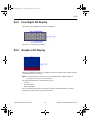
Graphic LCD Display . . . . . . . . . . . . . . . . . . . . . . . . . . . . . . . . . . . . . . . . . .
8-3
8-3
8-5
8-5
8.3
Virtual Terminal . . . . . . . . . . . . . . . . . . . . . . . . . . . . . . . . . . . . . . . . . . . . . . . . . . . . . 8-8
9. Misc. Digital Components
9.1
TIL Components. . . . . . . . . . . . . . . . . . . . . . . . . . . . . . . . . . . . . . . . . . . . . . . . . . . . . 9-1
9.1.1
AND Gate . . . . . . . . . . . . . . . . . . . . . . . . . . . . . . . . . . . . . . . . . . . . . . . . . . . 9-1
9.1.2
OR Gate . . . . . . . . . . . . . . . . . . . . . . . . . . . . . . . . . . . . . . . . . . . . . . . . . . . . 9-2
9.1.3
NOT Gate . . . . . . . . . . . . . . . . . . . . . . . . . . . . . . . . . . . . . . . . . . . . . . . . . . . 9-3
9.1.4
NOR Gate. . . . . . . . . . . . . . . . . . . . . . . . . . . . . . . . . . . . . . . . . . . . . . . . . . . 9-3
9.1.5
NAND Gate . . . . . . . . . . . . . . . . . . . . . . . . . . . . . . . . . . . . . . . . . . . . . . . . . 9-4
9.1.6
XOR Gate (Exclusive OR) . . . . . . . . . . . . . . . . . . . . . . . . . . . . . . . . . . . . . . 9-4
9.1.7
XNOR Gate (Exclusive NOR). . . . . . . . . . . . . . . . . . . . . . . . . . . . . . . . . . . . 9-5
9.1.8
Tristate Buffer . . . . . . . . . . . . . . . . . . . . . . . . . . . . . . . . . . . . . . . . . . . . . . . . 9-6
9.1.9
Buffer . . . . . . . . . . . . . . . . . . . . . . . . . . . . . . . . . . . . . . . . . . . . . . . . . . . . . . 9-6
9.1.10 Schmitt Trigger . . . . . . . . . . . . . . . . . . . . . . . . . . . . . . . . . . . . . . . . . . . . . . . 9-7
9.1.11 Digital Pulldown . . . . . . . . . . . . . . . . . . . . . . . . . . . . . . . . . . . . . . . . . . . . . . 9-8
9.1.12 Digital Pull-up . . . . . . . . . . . . . . . . . . . . . . . . . . . . . . . . . . . . . . . . . . . . . . . . 9-8
9.1.13 Digital State Machine . . . . . . . . . . . . . . . . . . . . . . . . . . . . . . . . . . . . . . . . . . 9-8
9.1.14 BCD_7SEG_DCD . . . . . . . . . . . . . . . . . . . . . . . . . . . . . . . . . . . . . . . . . . . . 9-9
9.1.15 Parity Generator/Checker. . . . . . . . . . . . . . . . . . . . . . . . . . . . . . . . . . . . . . . 9-9
9.1.16 Quad 2-to-1 Data Sel/MUX . . . . . . . . . . . . . . . . . . . . . . . . . . . . . . . . . . . . . 9-9
9.1.17 Digital Frequency Divider . . . . . . . . . . . . . . . . . . . . . . . . . . . . . . . . . . . . . . 9-10
9.2
VHDL . . . . . . . . . . . . . . . . . . . . . . . . . . . . . . . . . . . . . . . . . . . . . . . . . . . . . . . . . . . . 9-10
National Instruments Corporation
xv
Multisim Component Reference Guide
ComponentRef.book Page xvi Thursday, December 7, 2006 10:12 AM
9.3
Memory . . . . . . . . . . . . . . . . . . . . . . . . . . . . . . . . . . . . . . . . . . . . . . . . . . . . . . . . . . . 9-11
9.4
Line Receiver . . . . . . . . . . . . . . . . . . . . . . . . . . . . . . . . . . . . . . . . . . . . . . . . . . . . . . 9-11
9.5
Line Driver . . . . . . . . . . . . . . . . . . . . . . . . . . . . . . . . . . . . . . . . . . . . . . . . . . . . . . . . 9-11
9.6
Line Transceiver . . . . . . . . . . . . . . . . . . . . . . . . . . . . . . . . . . . . . . . . . . . . . . . . . . . 9-11
9.7
CPLDs. . . . . . . . . . . . . . . . . . . . . . . . . . . . . . . . . . . . . . . . . . . . . . . . . . . . . . . . . . . . 9-11
9.8
DSP Devices . . . . . . . . . . . . . . . . . . . . . . . . . . . . . . . . . . . . . . . . . . . . . . . . . . . . . . . 9-12
9.9
FPGA Devices . . . . . . . . . . . . . . . . . . . . . . . . . . . . . . . . . . . . . . . . . . . . . . . . . . . . . 9-12
9.10 Microcontrollers. . . . . . . . . . . . . . . . . . . . . . . . . . . . . . . . . . . . . . . . . . . . . . . . . . . . . 9-13
9.11 Programmable Logic Devices . . . . . . . . . . . . . . . . . . . . . . . . . . . . . . . . . . . . . . . . . . 9-13
9.12 Microprocessors . . . . . . . . . . . . . . . . . . . . . . . . . . . . . . . . . . . . . . . . . . . . . . . . . . . . 9-13
10. Mixed Components
10.1 ADC DAC . . . . . . . . . . . . . . . . . . . . . . . . . . . . . . . . . . . . . . . . . . . . . . . . . . . . . . . . . 10-1
10.1.1 Characteristic Equation . . . . . . . . . . . . . . . . . . . . . . . . . . . . . . . . . . . . . . . . 10-1
10.2 Analog Switch . . . . . . . . . . . . . . . . . . . . . . . . . . . . . . . . . . . . . . . . . . . . . . . . . . . . . 10-2
10.3 Timer . . . . . . . . . . . . . . . . . . . . . . . . . . . . . . . . . . . . . . . . . . . . . . . . . . . . . . . . . . . . 10-3
10.3.1 Model . . . . . . . . . . . . . . . . . . . . . . . . . . . . . . . . . . . . . . . . . . . . . . . . . . . . . 10-3
10.4 Mono Stable . . . . . . . . . . . . . . . . . . . . . . . . . . . . . . . . . . . . . . . . . . . . . . . . . . . . . . . 10-4
10.4.1 Model . . . . . . . . . . . . . . . . . . . . . . . . . . . . . . . . . . . . . . . . . . . . . . . . . . . . . 10-4
10.5 Phase-Locked Loop . . . . . . . . . . . . . . . . . . . . . . . . . . . . . . . . . . . . . . . . . . . . . . . . . 10-4
10.5.1 Characteristic Equation . . . . . . . . . . . . . . . . . . . . . . . . . . . . . . . . . . . . . . . . 10-5
10.5.2 Phase-Locked Loop Parameters and Defaults . . . . . . . . . . . . . . . . . . . . . . 10-6
10.6 Multivibrators. . . . . . . . . . . . . . . . . . . . . . . . . . . . . . . . . . . . . . . . . . . . . . . . . . . . . . . 10-6
10.6.1 CD4538BC . . . . . . . . . . . . . . . . . . . . . . . . . . . . . . . . . . . . . . . . . . . . . . . . . 10-6
10.6.2 SN74121N . . . . . . . . . . . . . . . . . . . . . . . . . . . . . . . . . . . . . . . . . . . . . . . . . 10-7
10.6.3 SN74123 . . . . . . . . . . . . . . . . . . . . . . . . . . . . . . . . . . . . . . . . . . . . . . . . . . 10-8
10.6.4 SN74130N . . . . . . . . . . . . . . . . . . . . . . . . . . . . . . . . . . . . . . . . . . . . . . . . . 10-8
10.7 Frequency Divider . . . . . . . . . . . . . . . . . . . . . . . . . . . . . . . . . . . . . . . . . . . . . . . . . . 10-8
Multisim Component Reference Guide
xvi
ni.com
ComponentRef.book Page xvii Thursday, December 7, 2006 10:12 AM
11. Indicators
11.1 Voltmeter . . . . . . . . . . . . . . . . . . . . . . . . . . . . . . . . . . . . . . . . . . . . . . . . . . . . . . . . . 11-1
11.2 Ammeter . . . . . . . . . . . . . . . . . . . . . . . . . . . . . . . . . . . . . . . . . . . . . . . . . . . . . . . . . 11-2
11.3 Digital Probe . . . . . . . . . . . . . . . . . . . . . . . . . . . . . . . . . . . . . . . . . . . . . . . . . . . . . . 11-2
11.4 Lamp . . . . . . . . . . . . . . . . . . . . . . . . . . . . . . . . . . . . . . . . . . . . . . . . . . . . . . . . . . . . 11-3
11.4.1 Time-Domain and AC Frequency Models . . . . . . . . . . . . . . . . . . . . . . . . . 11-3
11.5 Hex Displays . . . . . . . . . . . . . . . . . . . . . . . . . . . . . . . . . . . . . . . . . . . . . . . . . . . . . .
11.5.1 Seven-Segment Display . . . . . . . . . . . . . . . . . . . . . . . . . . . . . . . . . . . . . . .
11.5.2 Decoded Seven-Segment Display . . . . . . . . . . . . . . . . . . . . . . . . . . . . . . .
11.5.3 Alpha-Numeric Display . . . . . . . . . . . . . . . . . . . . . . . . . . . . . . . . . . . . . . .
11.5.4 DCD Hex Display . . . . . . . . . . . . . . . . . . . . . . . . . . . . . . . . . . . . . . . . . . .
11.5.5 Plus or Minus 1 LED Display . . . . . . . . . . . . . . . . . . . . . . . . . . . . . . . . . . .
11.5.6 Two Digit 7-Segment Display . . . . . . . . . . . . . . . . . . . . . . . . . . . . . . . . . . .
11.5.7 Duplexed Seven-Segment Display. . . . . . . . . . . . . . . . . . . . . . . . . . . . . . .
11-4
11-4
11-5
11-6
11-6
11-6
11-7
11-7
11.6 Bargraphs . . . . . . . . . . . . . . . . . . . . . . . . . . . . . . . . . . . . . . . . . . . . . . . . . . . . . . . . 11-7
11.6.1 Decoded Bargraph Display . . . . . . . . . . . . . . . . . . . . . . . . . . . . . . . . . . . . 11-8
11.7 Buzzer/Sonalert Buzzer . . . . . . . . . . . . . . . . . . . . . . . . . . . . . . . . . . . . . . . . . . . . . . 11-9
12. Power
12.1 SMPS Transient Virtual . . . . . . . . . . . . . . . . . . . . . . . . . . . . . . . . . . . . . . . . . . . . . . 12-1
12.1.1 PWMCM . . . . . . . . . . . . . . . . . . . . . . . . . . . . . . . . . . . . . . . . . . . . . . . . . . 12-1
12.1.2 PWMVM . . . . . . . . . . . . . . . . . . . . . . . . . . . . . . . . . . . . . . . . . . . . . . . . . . 12-3
12.1.3 PUSH_VM . . . . . . . . . . . . . . . . . . . . . . . . . . . . . . . . . . . . . . . . . . . . . . . . . 12-4
12.1.4 PUSH_CM . . . . . . . . . . . . . . . . . . . . . . . . . . . . . . . . . . . . . . . . . . . . . . . . . 12-6
12.1.5 HALF_VM . . . . . . . . . . . . . . . . . . . . . . . . . . . . . . . . . . . . . . . . . . . . . . . . . 12-7
12.1.6 HALF_CM . . . . . . . . . . . . . . . . . . . . . . . . . . . . . . . . . . . . . . . . . . . . . . . . . 12-9
12.1.7 FULL_CM . . . . . . . . . . . . . . . . . . . . . . . . . . . . . . . . . . . . . . . . . . . . . . . . 12-10
12.1.8 FULL_VM . . . . . . . . . . . . . . . . . . . . . . . . . . . . . . . . . . . . . . . . . . . . . . . . 12-12
12.1.9 2SWITCHCM . . . . . . . . . . . . . . . . . . . . . . . . . . . . . . . . . . . . . . . . . . . . . . 12-13
12.2 SMPS Average Virtual . . . . . . . . . . . . . . . . . . . . . . . . . . . . . . . . . . . . . . . . . . . . . .
12.2.1 BUCKCM . . . . . . . . . . . . . . . . . . . . . . . . . . . . . . . . . . . . . . . . . . . . . . . . .
12.2.2 BUCKCCM . . . . . . . . . . . . . . . . . . . . . . . . . . . . . . . . . . . . . . . . . . . . . . .
12.2.3 BOOSTCCM . . . . . . . . . . . . . . . . . . . . . . . . . . . . . . . . . . . . . . . . . . . . . .
12.2.4 BOOSTCM . . . . . . . . . . . . . . . . . . . . . . . . . . . . . . . . . . . . . . . . . . . . . . .
12.2.5 BOOSTDCM . . . . . . . . . . . . . . . . . . . . . . . . . . . . . . . . . . . . . . . . . . . . . .
12.2.6 BOOSTVM . . . . . . . . . . . . . . . . . . . . . . . . . . . . . . . . . . . . . . . . . . . . . . .
National Instruments Corporation
xvii
12-15
12-15
12-16
12-17
12-18
12-19
12-20
Multisim Component Reference Guide
ComponentRef.book Page xviii Thursday, December 7, 2006 10:12 AM
12.2.7
12.2.8
12.2.9
12.2.10
12.2.11
12.2.12
12.2.13
12.2.14
12.2.15
12.2.16
12.2.17
12.2.18
12.2.19
12.2.20
12.2.21
FLYBACKCCM . . . . . . . . . . . . . . . . . . . . . . . . . . . . . . . . . . . . . . . . . . . . . 12-21
BUCKDCM . . . . . . . . . . . . . . . . . . . . . . . . . . . . . . . . . . . . . . . . . . . . . . . . 12-22
BUCKVM . . . . . . . . . . . . . . . . . . . . . . . . . . . . . . . . . . . . . . . . . . . . . . . . . 12-23
FLYBACKCM . . . . . . . . . . . . . . . . . . . . . . . . . . . . . . . . . . . . . . . . . . . . . . 12-23
FLYBACKDCM . . . . . . . . . . . . . . . . . . . . . . . . . . . . . . . . . . . . . . . . . . . . . 12-24
FLYBACKVM . . . . . . . . . . . . . . . . . . . . . . . . . . . . . . . . . . . . . . . . . . . . . . 12-25
FWDCCM . . . . . . . . . . . . . . . . . . . . . . . . . . . . . . . . . . . . . . . . . . . . . . . . . 12-26
FORWARDCM . . . . . . . . . . . . . . . . . . . . . . . . . . . . . . . . . . . . . . . . . . . . . 12-27
FWDDCM . . . . . . . . . . . . . . . . . . . . . . . . . . . . . . . . . . . . . . . . . . . . . . . . . 12-28
FORWARDVM . . . . . . . . . . . . . . . . . . . . . . . . . . . . . . . . . . . . . . . . . . . . . 12-29
SEPICVM . . . . . . . . . . . . . . . . . . . . . . . . . . . . . . . . . . . . . . . . . . . . . . . . . 12-30
SEPICCM . . . . . . . . . . . . . . . . . . . . . . . . . . . . . . . . . . . . . . . . . . . . . . . . . 12-31
ERRAMP. . . . . . . . . . . . . . . . . . . . . . . . . . . . . . . . . . . . . . . . . . . . . . . . . . 12-32
AMPSIMP . . . . . . . . . . . . . . . . . . . . . . . . . . . . . . . . . . . . . . . . . . . . . . . . . 12-32
608PWM . . . . . . . . . . . . . . . . . . . . . . . . . . . . . . . . . . . . . . . . . . . . . . . . . . 12-32
12.3 Voltage Reference . . . . . . . . . . . . . . . . . . . . . . . . . . . . . . . . . . . . . . . . . . . . . . . . . 12-33
12.4 Voltage Regulator . . . . . . . . . . . . . . . . . . . . . . . . . . . . . . . . . . . . . . . . . . . . . . . . . . 12-33
12.4.1 Input/Output Voltage Differential Rating . . . . . . . . . . . . . . . . . . . . . . . . . . 12-34
12.5 Voltage Suppressor . . . . . . . . . . . . . . . . . . . . . . . . . . . . . . . . . . . . . . . . . . . . . . . . 12-34
12.6 Fuse . . . . . . . . . . . . . . . . . . . . . . . . . . . . . . . . . . . . . . . . . . . . . . . . . . . . . . . . . . . . 12-35
12.6.1 Characteristic Equations . . . . . . . . . . . . . . . . . . . . . . . . . . . . . . . . . . . . . . 12-35
12.6.2 Fuse Parameters and Defaults . . . . . . . . . . . . . . . . . . . . . . . . . . . . . . . . . 12-35
12.7 PWM Controllers . . . . . . . . . . . . . . . . . . . . . . . . . . . . . . . . . . . . . . . . . . . . . . . . . . 12-36
12.8 Miscellaneous Power . . . . . . . . . . . . . . . . . . . . . . . . . . . . . . . . . . . . . . . . . . . . . . . 12-36
12.9 Power Supply Controller . . . . . . . . . . . . . . . . . . . . . . . . . . . . . . . . . . . . . . . . . . . . 12-36
13. Misc. Components
13.1 Crystal . . . . . . . . . . . . . . . . . . . . . . . . . . . . . . . . . . . . . . . . . . . . . . . . . . . . . . . . . . . 13-1
13.2 DC Motor . . . . . . . . . . . . . . . . . . . . . . . . . . . . . . . . . . . . . . . . . . . . . . . . . . . . . . . . . 13-2
13.2.1 Characteristic Equations . . . . . . . . . . . . . . . . . . . . . . . . . . . . . . . . . . . . . . . 13-3
13.2.2 DC Motor Parameters and Defaults . . . . . . . . . . . . . . . . . . . . . . . . . . . . . . 13-4
13.3 Optocoupler . . . . . . . . . . . . . . . . . . . . . . . . . . . . . . . . . . . . . . . . . . . . . . . . . . . . . . . 13-4
13.4 Vacuum Tube . . . . . . . . . . . . . . . . . . . . . . . . . . . . . . . . . . . . . . . . . . . . . . . . . . . . . . 13-5
13.4.1 Characteristic Equations . . . . . . . . . . . . . . . . . . . . . . . . . . . . . . . . . . . . . . . 13-5
13.4.2 Model . . . . . . . . . . . . . . . . . . . . . . . . . . . . . . . . . . . . . . . . . . . . . . . . . . . . . 13-6
Multisim Component Reference Guide
xviii
ni.com
ComponentRef.book Page xix Thursday, December 7, 2006 10:12 AM
13.4.3
Triode Vacuum Tube Parameters and Defaults . . . . . . . . . . . . . . . . . . . . . 13-6
13.5 Boost Converter . . . . . . . . . . . . . . . . . . . . . . . . . . . . . . . . . . . . . . . . . . . . . . . . . . . 13-6
13.5.1 Characteristic Equations . . . . . . . . . . . . . . . . . . . . . . . . . . . . . . . . . . . . . . 13-7
13.5.2 Boost Converter Parameters and Defaults. . . . . . . . . . . . . . . . . . . . . . . . . 13-8
13.6 Buck Converter . . . . . . . . . . . . . . . . . . . . . . . . . . . . . . . . . . . . . . . . . . . . . . . . . . . . 13-8
13.6.1 Characteristic Equations . . . . . . . . . . . . . . . . . . . . . . . . . . . . . . . . . . . . . . 13-8
13.6.2 Buck Converter Parameters and Defaults . . . . . . . . . . . . . . . . . . . . . . . . . 13-9
13.7 Buck Boost Converter . . . . . . . . . . . . . . . . . . . . . . . . . . . . . . . . . . . . . . . . . . . . . . 13-10
13.7.1 Characteristic Equations . . . . . . . . . . . . . . . . . . . . . . . . . . . . . . . . . . . . . 13-10
13.7.2 Buck-Boost Converter Parameters and Defaults . . . . . . . . . . . . . . . . . . . 13-11
13.8 Lossy Transmission Line . . . . . . . . . . . . . . . . . . . . . . . . . . . . . . . . . . . . . . . . . . . . 13-11
13.8.1 Model . . . . . . . . . . . . . . . . . . . . . . . . . . . . . . . . . . . . . . . . . . . . . . . . . . . . 13-12
13.8.2 Lossy Transmission Line Model Parameters and Defaults . . . . . . . . . . . 13-13
13.9 Lossless Line Type 1 . . . . . . . . . . . . . . . . . . . . . . . . . . . . . . . . . . . . . . . . . . . . . . .
13.9.1 Model . . . . . . . . . . . . . . . . . . . . . . . . . . . . . . . . . . . . . . . . . . . . . . . . . . . .
13.9.2 Lossless Transmission Line Model Parameters and Defaults . . . . . . . . .
13.9.3 Lossless Line Type 2 . . . . . . . . . . . . . . . . . . . . . . . . . . . . . . . . . . . . . . . .
13-13
13-14
13-14
13-15
13.10 Net . . . . . . . . . . . . . . . . . . . . . . . . . . . . . . . . . . . . . . . . . . . . . . . . . . . . . . . . . . . . . 13-15
13.11 Filters . . . . . . . . . . . . . . . . . . . . . . . . . . . . . . . . . . . . . . . . . . . . . . . . . . . . . . . . . . . 13-15
13.12 Miscellaneous Components . . . . . . . . . . . . . . . . . . . . . . . . . . . . . . . . . . . . . . . . . . 13-16
13.13 MOSFET Driver . . . . . . . . . . . . . . . . . . . . . . . . . . . . . . . . . . . . . . . . . . . . . . . . . . . 13-16
13.14 Filters . . . . . . . . . . . . . . . . . . . . . . . . . . . . . . . . . . . . . . . . . . . . . . . . . . . . . . . . . . . 13-16
14. RF Components
14.1 RF Capacitor . . . . . . . . . . . . . . . . . . . . . . . . . . . . . . . . . . . . . . . . . . . . . . . . . . . . . . 14-1
14.2 RF Inductor . . . . . . . . . . . . . . . . . . . . . . . . . . . . . . . . . . . . . . . . . . . . . . . . . . . . . . . 14-2
14.3 RF Bipolar Transistors . . . . . . . . . . . . . . . . . . . . . . . . . . . . . . . . . . . . . . . . . . . . . . . 14-2
14.4 RF MOS_3TDN . . . . . . . . . . . . . . . . . . . . . . . . . . . . . . . . . . . . . . . . . . . . . . . . . . . . 14-3
14.5 Tunnel Diode . . . . . . . . . . . . . . . . . . . . . . . . . . . . . . . . . . . . . . . . . . . . . . . . . . . . . . 14-3
14.6 Strip Line . . . . . . . . . . . . . . . . . . . . . . . . . . . . . . . . . . . . . . . . . . . . . . . . . . . . . . . . . 14-4
14.7 Ferrite Beads . . . . . . . . . . . . . . . . . . . . . . . . . . . . . . . . . . . . . . . . . . . . . . . . . . . . . . 14-4
National Instruments Corporation
xix
Multisim Component Reference Guide
ComponentRef.book Page xx Thursday, December 7, 2006 10:12 AM
15. Electromechanical Components
15.1 Sensing Switches . . . . . . . . . . . . . . . . . . . . . . . . . . . . . . . . . . . . . . . . . . . . . . . . . . . 15-1
15.2 Supplementary Contacts . . . . . . . . . . . . . . . . . . . . . . . . . . . . . . . . . . . . . . . . . . . . . 15-1
15.3 Momentary Switches . . . . . . . . . . . . . . . . . . . . . . . . . . . . . . . . . . . . . . . . . . . . . . . . 15-2
15.4 Line Transformer . . . . . . . . . . . . . . . . . . . . . . . . . . . . . . . . . . . . . . . . . . . . . . . . . . . 15-2
15.5 Coils, Relays . . . . . . . . . . . . . . . . . . . . . . . . . . . . . . . . . . . . . . . . . . . . . . . . . . . . . . 15-3
15.6 Timed Contacts . . . . . . . . . . . . . . . . . . . . . . . . . . . . . . . . . . . . . . . . . . . . . . . . . . . . 15-3
15.7 Protection Devices . . . . . . . . . . . . . . . . . . . . . . . . . . . . . . . . . . . . . . . . . . . . . . . . . . 15-4
15.8 Output Devices . . . . . . . . . . . . . . . . . . . . . . . . . . . . . . . . . . . . . . . . . . . . . . . . . . . . 15-4
15.9 Pilot Lights . . . . . . . . . . . . . . . . . . . . . . . . . . . . . . . . . . . . . . . . . . . . . . . . . . . . . . . . 15-4
15.10 Terminals . . . . . . . . . . . . . . . . . . . . . . . . . . . . . . . . . . . . . . . . . . . . . . . . . . . . . . . . . 15-5
Appendix A
A.1
Technical Support and Professional Services . . . . . . . . . . . . . . . . . . . . . . . . . . . . . .A-1
Multisim Component Reference Guide
xx
ni.com
ComponentRef.book Page 1 Thursday, December 7, 2006 10:12 AM
Chapter 1
Source Components
1.1
Ground
A voltage measurement is always referenced to some point, since a voltage is actually a
“potential difference” between two points in a circuit.
The concept of “ground” is a way of defining a point common to all voltages. It represents 0
volts. All voltage levels around the circuit are positive or negative when compared to ground.
In power systems, the planet Earth itself is used for this reference point (most home power
circuits are ultimately “grounded” to the Earth's surface for lightning protection). This is how
the expression “earthing” or “grounding” a circuit originated.
Most modern power supplies have “floating” positive and negative outputs, and either output
point can be defined as ground. These types of supplies can be used as positive (with respect
to ground) or negative power supplies. In floating power supply circuits, the positive output is
often used as the voltage reference for all parts of the circuit.
Note Multisim supports a multipoint grounding system. Each ground connected is made
directly to the ground plane.
The Ground Component
This component has 0 voltage and so provides a clear reference point for calculating electrical
values. You can use as many ground components as you want. All terminals connected to
ground components represent a common point and are treated as joined together.
Not all circuits require grounding for simulation; however, any circuit that uses an opamp,
transformer, controlled source or oscilloscope must be grounded. Also, any circuit which
contains both analog and digital components should be grounded. If a circuit is ungrounded or
improperly grounded (even if it does not need grounding in reality), it may not be simulated.
If it is simulated, it may produce inconsistent results. The linear transformer must be
grounded on both sides.
National Instruments Corporation
1-1
Multisim Component Reference Guide
ComponentRef.book Page 2 Thursday, December 7, 2006 10:12 AM
Source Components
1.2
Digital Ground
The digital ground is used to ground digital components which do not have an explicit ground
pin. The digital ground must be placed on the schematic but does not need to be connected
directly to any component.
Tip If you are unsure of the ground required for a digital component that has its ground pin
hidden, double-click on the component and click on the Pins tab. Locate GND in the
Name column and move across to the Net column. In most cases, the name of the net will
be GND.
The default Reference Designator (RefDes) for the digital ground is GND. When you connect
a wire to a digital ground, the wire’s net name will be the same as the digital ground’s RefDes.
Multiple instances of a digital ground may be placed on a schematic but there will only be one
matching net in the schematic.
If you rename a digital ground by changing its RefDes, and there are other instances of the
digital ground with the same RefDes on the schematic, you will be prompted to confirm that
you want to change all instances of the RefDes. If you select No, only the RefDes for the
selected digital ground will change. Remember that if a digital ground’s RefDes is changed,
the net name of any wires attached to it will change to match the new RefDes. For a more
detailed discussion, see “Global Nets” in the Multisim User Guide, or the Multisim helpfile.
To change the RefDes of a digital ground:
1. Double-click on the component to display its properties dialog box, and click on the Label
tab.
2. Change the entry in the RefDes field and click OK to close the dialog box.
1.3
DC Voltage Source (Battery)
Battery Background Information
A battery may be a single electrochemical cell or a number of electrochemical cells wired in
series. It is used to provide a direct source of voltage and/or current.
Multisim Component Reference Guide
1-2
ni.com
ComponentRef.book Page 3 Thursday, December 7, 2006 10:12 AM
Digital Power Supplies
A single cell has a voltage of approximately 1.5 volts, depending on its construction. It
consists of a container of acid in which an electrode is placed. Chemical action causes
electrons to flow between the electrode and the container, and this creates a potential
difference between the electrode and the material of the container.
Batteries can be rechargeable and can be built to deliver extremely high currents for long
periods. The automobile ignition battery is an application of a battery as a “current source”;
the voltage may vary considerably under use, with no visible battery deterioration.
Batteries may be used as voltage references, their voltage remaining stable and predictable to
many figures of accuracy for many years. The standard cell is such an application. A standard
cell is a voltage source, and it is important that current is not drawn from the standard cell.
Battery Component
Multisim includes both an ideal battery (DC_POWER), with no internal resistance and a nonideal battery, that allows you to changes its internal resistance and capacity (in ampere hours).
1.4
Digital Power Supplies
The Power Source component family includes the digital power supplies VCC, VDD, VEE,
and VSS. These are used to connect power to digital components which do not have an
explicit power pin on their symbol. They can also be wired directly into a circuit as desired.
Tip If you are unsure of the power supply required for a digital component that has its power
pin hidden, double-click on the component and click on the Pins tab. Locate the power
supply in the Name column. Some components, will have more than one power supply
(for example, a CMOS 4522BD has both VDD and VSS).
When you connect a wire to a digital power supply (for example, VCC), the wire’s net name
will be the same as the digital supply’s RefDes (so in the case of VCC, the net name will be
VCC). Multiple instances of a digital power supply may be placed on a schematic but there
will only be one matching net in the schematic. Also, when you change a digital power
supply’s voltage, the voltage for all instances of that power supply on the schematic will
change to reflect the new setting.
National Instruments Corporation
1-3
Multisim Component Reference Guide
ComponentRef.book Page 4 Thursday, December 7, 2006 10:12 AM
Source Components
If you rename a digital power supply by changing its RefDes, and there are other instances of
the same supply on the schematic, you will be prompted to confirm that you want to change
all instances of the RefDes. If you select No, only the RefDes for the selected component will
change. Remember that if a digital power supply’s RefDes is changed, the net name of any
wires attached to it will change to match the new RefDes. For a more detailed discussion, see
“Global Nets” in the Multisim User Guide, or the Multisim helpfile.
To change the properties of a digital power supply:
1. Double-click on the component to display its properties dialog box, and click on the Value
tab. Change the value in the Voltage (V) field as desired.
2. To change the reference designator for the component, click on the Label tab and change
the entry in the RefDes field.
3. Click OK to close the dialog box.
1.5
DC Current Source
The current generated by this source can be adjusted from microamps to kiloamps.
1.6
AC Voltage Source
The root-mean-square (RMS) voltage of this source can be adjusted from µV to kilovolts. You
can also control its frequency and phase angle.
VRMS =
V peak
2
Multisim Component Reference Guide
1-4
ni.com
ComponentRef.book Page 5 Thursday, December 7, 2006 10:12 AM
AC Current Source
1.7
AC Current Source
The RMS current of this source can be adjusted from microamps to kiloamps. You can also
control its frequency and phase angle.
IR MS =
1.8
I peak
2
Clock Source
This component is a square wave generator. You can adjust its voltage amplitude, duty cycle
and frequency.
1.9
Amplitude Modulation (AM) Source
The AM source (single-frequency amplitude modulation source) generates an amplitudemodulated wave. It can be used to build and analyze communications circuits.
National Instruments Corporation
1-5
Multisim Component Reference Guide
ComponentRef.book Page 6 Thursday, December 7, 2006 10:12 AM
Source Components
1.9.1
Characteristic Equation
The behavior of the AM source is described by:
VOUT = vc∗ sin(2∗ π ∗ fc∗ TIME )∗ (1 + m∗ sin( 2∗ π ∗ fm∗ TIME ))
where:
vc = carrier amplitude, in volts
fc = carrier frequency, in hertz
m = modulation index
fm = modulation frequency, in hertz
1.10
FM Source
The FM source (single-frequency frequency modulation source) generates a frequencymodulated wave. It can be used to build and analyze communications circuits.The signal
output can be either a current source or a voltage source.
1.10.1 FM Voltage Source
This is an FM source of which the output is measured in voltage.
1.10.2 Characteristic Equation
The behavior of the FM voltage source is described by:
VOUT = va∗ sin( 2∗ π ∗ fc∗ TIME + m∗ sin(2∗ π ∗ fm∗ TIME ))
where:
va = peak amplitude, in volts
fc = carrier frequency, in Hz
m = modulation index
fm = modulation frequency, in Hz
Multisim Component Reference Guide
1-6
ni.com
ComponentRef.book Page 7 Thursday, December 7, 2006 10:12 AM
FSK Source
1.10.3 FM Current Source
This component is the same as the FM voltage source, except that the output is measured in
current.
1.10.4 Characteristic Equation
The behavior of the FM current source is described by the same equation as in the FM Voltage
Source, with Vout replaced by Iout.
1.11
FSK Source
This source is used for keying a transmitter for telegraph or teletype communications by
shifting the carrier frequency over a range of a few hundred hertz. The frequency shift key
(FSK) modulated source generates the mark transmission frequency, f1, when a binary 1 is
sensed at the input, and the space transmission frequency, f2, when a 0 is sensed.
FSK is used in digital communications systems such as in low speed modems (for example, a
Bell 202 type modem - 1200 baud or less).
In this system, a digital high level is referred to as a MARK and is reproduced as a frequency
of 1200 Hz. A digital low level is referred to as a SPACE and is represented by a frequency of
2200 Hz.
In the example shown below, the frequency shift keying signal is a 5v (TTL) square wave.
National Instruments Corporation
1-7
Multisim Component Reference Guide
ComponentRef.book Page 8 Thursday, December 7, 2006 10:12 AM
Source Components
When the keying input is 5V, a MARK frequency of 1200 Hz is output. When keying voltage
is 0V, a SPACE frequency of 2200 Hz is output.
This component is a square wave generator. You can adjust its voltage amplitude, duty cycle
and frequency.
1.12
Voltage-Controlled Voltage Source
The output voltage of this source depends on the voltage applied to its input terminal. The
ratio of the output voltage to the input voltage determines its voltage gain (E). Voltage gain
can have any value from mV/V to kV/V.
E=
V OUT
V IN
Multisim Component Reference Guide
1-8
ni.com
ComponentRef.book Page 9 Thursday, December 7, 2006 10:12 AM
Current-Controlled Voltage Source
1.13
Current-Controlled Voltage Source
The output voltage of this source depends on the current through the input terminals. The two
are related by a parameter called transresistance (H), which is the ratio of the output voltage to
the input current. It can have any value from mW to kW.
H =
1.14
V OUT
I IN
Voltage-Controlled Current Source
The output current of this source depends on the voltage applied at the input terminals. The
two are related by a parameter called transconductance (G), which is the ratio of the output
current to the input voltage. It is measured in mhos (also known as seimens) and can have any
value from mmhos to kmhos.
G=
1.15
I OUT
V IN
Current-Controlled Current Source
The magnitude of the current output of a current-controlled current source depends on the
current through the input terminals. The two are related by a parameter called current gain (F),
National Instruments Corporation
1-9
Multisim Component Reference Guide
ComponentRef.book Page 10 Thursday, December 7, 2006 10:12 AM
Source Components
which is the ratio of the output current to the input current. The current gain can have any
value from mA/A to kA/A.
F=
1.16
I OUT
I IN
Voltage-Controlled Sine Wave
This oscillator takes an input AC or DC voltage, which it uses as the independent variable in
the piecewise linear curve described by the (control, frequency) pairs. From the curve, a
frequency value is determined, and the oscillator outputs a sine wave at that frequency. When
only two co-ordinate pairs are used, the oscillator outputs a linear variation of the frequency
with respect to the control input. When the number of co-ordinate pairs is greater than two,
the output is piecewise linear. You can change the peak and valley values of the output sine
wave by resetting the Output peak high value and Output peak low value on the model
parameter dialog box.
Example
The example shows a sine wave generator with output frequency determined by a control
voltage.
Control voltage may be DC, controlled by a potentiometer, as is the case for many signal
generators and function generators, or may be the output from a PLL that determines a precise
frequency.
Control voltage may be a continuous variable of any desired shape as required in sweep
generators and spectrum analysers.
In the example shown below, the VCO parameters are set so that control voltage of 0V
produces an output frequency of 100Hz and a control voltage of 12V produces an output
frequency of 20KHz.
Multisim Component Reference Guide
1-10
ni.com
ComponentRef.book Page 11 Thursday, December 7, 2006 10:12 AM
Voltage-Controlled Square Wave
A square wave control voltage produces a form of FSK (frequency shift keying), a sine wave
control voltage produces a form of FM (frequency modulation).
1.17
Voltage-Controlled Square Wave
This oscillator is identical to the voltage-controlled sine wave oscillator except that it outputs
a square wave. This oscillator takes an input AC or DC voltage, which it uses as the
independent variable in the piecewise linear curve described by the (control, frequency) pairs.
From the curve, a frequency value is determined, and the oscillator outputs a square wave at
that frequency. When two co-ordinate pairs are used, the oscillator outputs a linear variation
of the frequency with respect to the control input. When the number of co-ordinate pairs is
greater than two, the output is piecewise linear. You can change duty cycle, rise and fall times,
and the peak and valley values of the output square wave by resetting the Output peak high
value and Output peak low value on the model parameter dialog box.
National Instruments Corporation
1-11
Multisim Component Reference Guide
ComponentRef.book Page 12 Thursday, December 7, 2006 10:12 AM
Source Components
Example
The example shows a square wave generator with output frequency determined by a control
voltage.
Control voltage may be DC, controlled by a potentiometer, as is the case for many signal
generators and function generators.
Control voltage may be a continuous variable of any desired shape as required in sweep
generators and spectrum analysers.
In the example shown below, the VCO parameters are set so that control voltage of 0V
produces an output frequency of 100Hz and control voltage of 12V produces an output
frequency of 20KHz.
A square wave control voltage produces a form of FSK (frequency shift keying), a sine wave
control voltage produces a form of FM (frequency modulation).
Multisim Component Reference Guide
1-12
ni.com
ComponentRef.book Page 13 Thursday, December 7, 2006 10:12 AM
Voltage-Controlled Triangle Wave
1.18
Voltage-Controlled Triangle Wave
This oscillator is identical to the voltage-controlled sine wave oscillator except that it outputs
a triangle wave. This oscillator takes an input AC or DC voltage, which it uses as the
independent variable in the piecewise linear curve described by the (control, frequency) pairs.
From the curve, a frequency value is determined, and the oscillator outputs a triangle wave at
that frequency. When two co-ordinate pairs are used, the oscillator outputs a linear variation
of the frequency with respect to the control input. When the number of co-ordinate pairs is
greater than two, the output is piecewise linear. You can change the rise time duty cycle and
the peak and valley values of the output triangle wave by resetting the Output peak high value
and Output peak low value on the model parameter dialog box.
Example
The example shows a triangle wave generator with output frequency determined by a control
voltage.
Control voltage may be DC, controlled by a potentiometer, as is the case for many signal
generators and function generators.
Control voltage may be a continuous variable of any desired shape as required in sweep
generators and spectrum analysers.
In the example shown below, the VCO parameters are set so that control voltage of 0V
produces an output frequency of 100Hz and control voltage of 12V produces an output
frequency of 20KHz.
National Instruments Corporation
1-13
Multisim Component Reference Guide
ComponentRef.book Page 14 Thursday, December 7, 2006 10:12 AM
Source Components
A square wave control voltage produces a form of FSK (frequency shift keying), a sine wave
control voltage produces a form of FM (frequency modulation).
1.19
Voltage-Controlled Piecewise Linear Source
This source (voltage-controlled piecewise linear source) allows you to control the shape of the
output waveform by entering up to five (input, output) pairs, which are shown in the Value tab
of the component’s properties dialog box as (X,Y) co-ordinates.
The X values are input co-ordinate points and the associated Y values represent the outputs of
those points. If you use only two pairs, the output voltage is linear.
Outside the bounds of the input co-ordinates, the source extends the slope found between the
lowest two co-ordinate pairs and the highest two co-ordinate pairs. A potential effect of this
behavior is that it can unrealistically cause the output to reach a very large or very small value,
Multisim Component Reference Guide
1-14
ni.com
ComponentRef.book Page 15 Thursday, December 7, 2006 10:12 AM
Piecewise Linear Source
especially for large input values. Therefore, keep in mind that this source does not inherently
provide a limiting capability.
In order to reduce the potential for non-convergence of simulations, the source provides for
smoothing around the co-ordinate pairs. If Input smoothing domain (ISD) is set to, say, 10%,
the simulator assumes a smoothing radius about each co-ordinate point equal to 10% of the
length of the smaller of the segments above and below each co-ordinate point.
1.20
Piecewise Linear Source
The Piecewise Linear Source (PWL) is available as either a voltage source or a current source.
This source allows you to control the shape of the waveform by entering pairs of time and
voltage/current values. Each pair specifies the value of the source at the specified time. At
intermediate values of time, the value of the source is determined by linear interpolation.
The component also reads a specified file which contains a table of time and current or
voltage points. Using the data in the table, the component generates a current or voltage
waveform specified by the input text file.
To set up the PWL source:
1. Double-click on the PWL Source to open its properties dialog box.
2. From the Value tab, either select the file containing the time and voltage or current points
from the dialog box or enter the data points manually.
Refer to the following for details on each type of PWL Source:
• “Piecewise Linear Voltage Source” on page 1-17
• “Piecewise Linear Current Source” on page 1-17.
National Instruments Corporation
1-15
Multisim Component Reference Guide
ComponentRef.book Page 16 Thursday, December 7, 2006 10:12 AM
Source Components
1.20.1 PWL Source Input Text File Specification
This file must contain a list of time and voltage or current points. Each line of the file
represents one point. The format is:
Time <space(s)> Voltage or Time <space(s)> Current
You can leave any amount of space between the Time and Voltage/Current fields. Here is an
example of an ideally formatted input file:
0
0
2.88e-06
0.0181273
5.76e-06
0.0363142
1e-05
0.063185
1.848e-05
0.117198
If the PWL source encounters...
It will...
non-whitespace at beginning of line
ignore the line
non-numeric data following correctly formatted
data
accept data, ignore nonnumeric data
non-whitespace between Time and Voltage/
Current
ignore the line
whitespace preceding correctly formatted data
accept data, ignore
whitespace
Please note the following special considerations:
•
•
•
•
If the earliest input point is not at time 0.0, then the PWL source gives the output of the
earliest time point from time 0.0 to that earliest time.
After the latest input point, the PWL source gives the output of the latest time point in the
file from that latest time until the simulation ends.
Between input points, the PWL source uses linear interpolation to generate output.
The PWL source can handle unsorted data. It sorts the points by time before the simulation
starts.
Multisim Component Reference Guide
1-16
ni.com
ComponentRef.book Page 17 Thursday, December 7, 2006 10:12 AM
Piecewise Linear Source
1.20.2 Piecewise Linear Voltage Source
This component is a piecewise linear source with a voltage output.
The Value tab in this component’s properties dialog box contains the following:
The Use data directly from file radio button, used if your data pairs are in a separate .txt
file. If you choose this option, the circuit will depend on the text file. When this button is
selected the following become active:
• Filename — click on the button to the right of this field and navigate to the data file.
The data file must have a .txt extension to be used.
Note If you do not specify a filename, the PWL voltage source behaves like a short circuit.
An error message does not display in this case.
•
•
•
• Edit file — click to open the data file for editing.
The Enter data points in table radio button, used if you wish to manually enter the data
pairs, without referencing an external file. If you choose this option, the following become
active:
• Time and Voltage columns — where you enter the desired time and voltage data points.
• Initialize from file — click to view the data pairs from a specific file. If you choose this
option, the circuit will not depend on the text file. The data points will be loaded and
saved into the circuit file.
Repeat data during simulation — enable to continuously run the file during simulation. If
this checkbox is not enabled, output from the source will cease once the final data pair has
been read.
1.20.3 Piecewise Linear Current Source
This component is a piecewise linear source with a current output.
The Value tab in this component’s properties dialog box contains the following:
•
The Use data directly from file radio button, used if your data pairs are in a separate .txt
National Instruments Corporation
1-17
Multisim Component Reference Guide
ComponentRef.book Page 18 Thursday, December 7, 2006 10:12 AM
Source Components
file. If you choose this option, the circuit will depend on the text file. When this button is
selected the following become active:
• Filename — click on the button to the right of this field and navigate to the data file.
The data file must have a .txt extension to be used.
Note If you do not specify a filename, the output of the PWL current source behaves like an
open circuit. An error message does not display in this case.
•
•
1.21
• Edit file — click to open the data file for editing.
The Enter data points in table radio button, used if you wish to manually enter the data
pairs, without referencing an external file. If you choose this option, the following become
active:
• Time and Current columns — where you enter the desired time and current data points.
• Initialize from file — click to view the data pairs from a specific file. If you choose this
option, the circuit will not depend on the text file. The data points will be loaded and
saved into the circuit file.
Repeat data during simulation — enable to continuously run the file during simulation. If
this checkbox is not enabled, output from the source will cease once the final data pair has
been read.
Pulse Source
This source includes pulse voltage source and pulse current source.The Pulse sources are
configurable sources whose output can be set to produce periodic pulses.
The following parameters can be modified:
•
•
•
•
•
•
•
Initial Value
Pulsed Value
Delay time
Rise Time
Fall time
Pulse Width
Period
Multisim Component Reference Guide
1-18
ni.com
ComponentRef.book Page 19 Thursday, December 7, 2006 10:12 AM
Polynomial Source
1.21.1 Pulse Voltage Source
This component is a pulse source of which the output is measured in voltage.
1.21.2 Pulse Current Source
This component is the same as the Pulse Voltage Source, except that the output is measured in
current.
1.22
Polynomial Source
This is a voltage-controlled voltage source defined by a polynomial transfer function. It is a
specific case of the more general nonlinear dependent source. Use it for analog behavioral
modeling.
The polynomial source has three controlling voltage inputs, namely, V1, V2 and V3.
Output Voltage Characteristic Equation
The output voltage is given by:
VOUT = A + B∗V 1 + C∗V 2 + D∗V 3 + E ∗V 12 + F ∗V 1∗V 2 + G∗V 1∗V 3
+ H ∗V 2 2 + I ∗V 2∗V 3 + J ∗V 3 2 + K ∗V 1∗V 2∗V 3
National Instruments Corporation
1-19
Multisim Component Reference Guide
ComponentRef.book Page 20 Thursday, December 7, 2006 10:12 AM
Source Components
where:
A = constant
B = coefficient of V1
C = coefficient of V2
D = coefficient of V3
E = coefficient of V1²
F = coefficient of V1*V2
G = coefficient of V1*V3
H = coefficient of V2²
I = coefficient of V2*V3
J = coefficient of V3²
K = coefficient of V1*V2*V3
1.23
Exponential Source
The exponential sources are configurable sources whose output can be set to produce an
exponential signal.
The following parameters can be modified:
•
•
•
•
•
•
Initial Value
Pulsed Value
Rise Delay time
Rise Time
Fall Delay time
Fall Time
1.23.1 Exponential Voltage Source
This component is an exponential source of which the output is measured in voltage.
Multisim Component Reference Guide
1-20
ni.com
ComponentRef.book Page 21 Thursday, December 7, 2006 10:12 AM
Nonlinear Dependent Source
1.23.2 Exponential Current Source
This component is the same as the Exponential Voltage Source, except that the output is
measured in current.
1.24
Nonlinear Dependent Source
Use this source for analog behavioral modeling. This generic source allows you to create a
sophisticated behavioral model by entering a mathematical expression.
This source uses analog behavioral modeling through mathematical expressions.
The output voltage or current can be a function of up to four voltages and two currents.
Voltages and currents are referenced by connecting the input pins of this device to schematic
nodes.
For a more flexible solution, see “ABM Sources” on page 1-49.
To change the nonlinear dependent source’s value:
1. Double-click on the placed component and click the Value tab.
2. Complete the Source Expression.
Note If you set the dependent variable to “V”, the output is in voltage; if you set it to “I”, the
output is in current.
1.25
Controlled One-Shot
This oscillator takes an AC or DC input voltage, which it uses as the independent variable in
the piecewise linear curve described by the (control, pulse width) pairs. From the curve, a
pulse width value is determined, and the oscillator outputs a pulse of that width. You can
National Instruments Corporation
1-21
Multisim Component Reference Guide
ComponentRef.book Page 22 Thursday, December 7, 2006 10:12 AM
Source Components
change clock trigger value, output delay from trigger, output delay from pulse width, output
rise and fall times, and output high and low values.
When only two co-ordinate pairs are used, the oscillator outputs a linear variation of the pulse
with respect to the control input. When the number of co-ordinate pairs is greater than two,
the output is piecewise linear.
1.26
Magnetic Flux Source
This device is used with a Hall Effect Sensor.
The Magnetic Flux Source uses the “B” key to change the density and polarity of the
magnetic flux impacting on a Hall Effect Sensor. You must specify the sphere of influence of
the magnetic flux source by entering an integer value in the Magnetic Channel field in the
Value tab of the component’s properties screen.
The Magnetic Channel field on the Hall Effect Sensor must have a matching integer value for
that sensor to be influenced by the source. No two magnetic flux sources or generators should
have the same integer value in the Magnetic Channel field. You can have as many Hall Effect
Sensors as you wish to react to any given source/generator and as many different sources/
generators as desired as long as each source/generator has a different integer value.
1.27
Magnetic Flux Generator
This device is used with a Hall Effect Sensor.
The Magnetic Flux Generator produces a continuous varying magnetic field (sinusoidal with
N and S peaks). You can define the flux density, rate of rotation (translating to frequency) and
specify the sphere of influence of the generator by putting a unique integer value in the
Magnetic Channel field in the Value tab of the source’s properties screen.
Multisim Component Reference Guide
1-22
ni.com
ComponentRef.book Page 23 Thursday, December 7, 2006 10:12 AM
Multiplier
The Magnetic Channel field on the Hall Effect Sensor must have a matching integer value for
that sensor to be influenced by the generator. No two magnetic flux generators or sources
should have the same integer value in the Magnetic Channel field. You can have as many Hall
Effect Sensors as you wish to react to any given source/generator and as many different
sources/generators as desired as long as each source/generator has a different integer value.
1.28
Multiplier
This component multiplies two input voltages.
The basic function multiplies the X and Y inputs.
Vo = Vx * Vy
Gain factors may be applied to the X and Y inputs and to the output.
Examples shown below:
a) Two DC voltages are multiplied (4V * 2V = 8V)
b) Two volts DC multiplied by 2 V peak
c) Two AC signals
National Instruments Corporation
1-23
Multisim Component Reference Guide
ComponentRef.book Page 24 Thursday, December 7, 2006 10:12 AM
Source Components
Characteristic Equation
The output voltage is given by:
( (
) (
Vout = K X K Vx + X off ∗ Yk Vy + Yoff
) ) + off
where:
Vx = input voltage at x
Vy = input voltage at y
Other symbols used in these equations are defined in “Multiplier Parameters and Defaults”.
Multisim Component Reference Guide
1-24
ni.com
ComponentRef.book Page 25 Thursday, December 7, 2006 10:12 AM
Divider
Multiplier Parameters and Defaults
1.29
Symbol
Parameter Name
Default
Unit
k
Output gain
0.1
V/V
off
Output
0.0
V
Yoff
Y offset
0.0
V
Yk
Y gain
1.0
V/V
Xoff
X offset
0.0
V
Xk
X gain
1.0
V/V
Divider
This component divides one voltage (the y input, or numerator) by another (the x input, or
denominator).
Vo = Vy/Vx
You can limit the value of the denominator input to a value above zero by using the parameter
XLowLim. This limit is approached through a quadratic smoothing function, the domain of
which you can specify as an absolute value in XDS.
In the example shown below, the 120v RMS (339.38v peak to peak) sine wave at the Y input
is divided by a 16.96V DC voltage at the X input. The result is 339.38v (peak to peak) /
16.97V = 20v peak to peak.
If Vx is replaced with a 12v RMS voltage, in phase with Vy, the output will be 10V DC.
National Instruments Corporation
1-25
Multisim Component Reference Guide
ComponentRef.book Page 26 Thursday, December 7, 2006 10:12 AM
Source Components
CAUTION If the X (denominator) voltage crosses 0v when any voltage is present at the Y
(numerator) terminal, the quotient will go to infinity and a large positive or negative “spike”
will be observed on the scope.
Characteristic Equation
(
)
)
Vy + Yoff ∗ Yk
∗ k + off
Vout =
V
+
X
∗
X
x
off
k
(
where:
Vx = input voltage at x
Vy = input voltage at y
Other symbols used in these equations are defined in the table below.
Multisim Component Reference Guide
1-26
ni.com
ComponentRef.book Page 27 Thursday, December 7, 2006 10:12 AM
Transfer Function Block
Divider Parameters and Defaults
1.30
Symbol
Parameter Name
Default
Unit
k
Output gain
1
V/V
off
Output offset
0
V
Yoff
Y (Numerator) offset
0
V
Yk
Y (Numerator) gain
1
V/V
Xoff
X (Denominator) offset
0
V
Xk
X (Denominator) gain
1
V/V
XLowLim
X (Denominator) lower limit
100
pV
XSD
X (Denominator) smoothing domain
100
pV
Transfer Function Block
This component models the transfer characteristic of a device, circuit or system in the s
domain. The transfer function block is specified as a fraction with polynomial numerators and
denominators. A transfer function up to the third order can be directly modeled. This
component may be used in DC, AC and transient analyses.
Characteristic Equation
This transfer function model is defined in a form of the rational function:
T ( s) =
A s 3 + A2 s 2 + A1 s + A0
Y ( s)
= K∗ 3 3
X ( s)
B3 s + B2 s 2 + B1 s + B0
Transfer functions up to the third order may be modeled.
National Instruments Corporation
1-27
Multisim Component Reference Guide
ComponentRef.book Page 28 Thursday, December 7, 2006 10:12 AM
Source Components
In the example shown below, the transfer function for a simple first order low pass filter is
used. Only the numerator and denominator constants A0 and B0 are required in this case.
These are equal to two pi times the cutoff frequency (first pole).
The cursor on the Bode Plotter may be used to confirm first order performance with -3dB at
10kHz. and rolloff of 6dB per octave above 20kHz.
Transfer Function Block Parameters and Defaults
Symbol
Parameter Name
Default
Unit
VIoff
Input voltage offset
0
V
K
Gain
1
V/V
VINT
Integrator stage initial conditions
0
V
w
Denormalized corner frequency
1
-
A3
Numerator 3rd order coefficient
0
-
A2
Numerator 2nd order coefficient
0
-
A1
Numerator 1st order coefficient
0
-
A0
Numerator constant
1
-
Multisim Component Reference Guide
1-28
ni.com
ComponentRef.book Page 29 Thursday, December 7, 2006 10:12 AM
Voltage Gain Block
1.31
Symbol
Parameter Name
Default
Unit
B3
Denominator 3rd order coefficient
0
-
B2
Denominator 2nd order coefficient
0
-
B1
Denominator 1st order coefficient
0
-
B0
Denominator constant
1
-
Voltage Gain Block
This component multiplies the input voltage by the gain and delivers it to the output. This
represents a voltage amplifier function with the gain factor, K, selectable with the Value tab of
the component’s properties screen. The voltage gain block is used in control systems and
analog computing applications.
In the example shown below, the input is a 0.707v RMS (2v peak to peak) sine wave and the
gain factor K is set at 5. The output then is K times the input.
(.707*5= 3.535v RMS or 10 v peak to peak)
Caution Using the default model, as in this example, sine wave inputs
may be any value.
National Instruments Corporation
1-29
Multisim Component Reference Guide
ComponentRef.book Page 30 Thursday, December 7, 2006 10:12 AM
Source Components
Suitable settings of model parameters will allow for virtually unlimited flexibility for
practical applications.
Characteristic Equation
Vout = K (Vin + VIoff ) + VOoff
Voltage Gain Block Parameters and Defaults
Symbol
Parameter Name
Default
Unit
K
Gain
1
V/V
VIoff
Input offset voltage
0
V
VOoff
Output offset voltage
0
V
Multisim Component Reference Guide
1-30
ni.com
ComponentRef.book Page 31 Thursday, December 7, 2006 10:12 AM
Voltage Differentiator
1.32
Voltage Differentiator
This component calculates the derivative of the input voltage (the transfer function, s) and
delivers it to the output. It is used in control systems and analog computing applications.
Differentiation may be described as a “rate of change” function and defines the slope of a
curve.
Rate of change = dV/dT
Characteristic Equation
Vout (t ) = K
dVi
+ VOoff
dt
Voltage Differentiator Parameters and Defaults
Symbol
Parameter Name
Default
Unit
K
Gain
1
V/V
VOoff
Output offset voltage
0
V
Vl
Output voltage lower limit
-1e+12
V
Vu
Output voltage upper limit
1e+12
V
Vs
Upper and lower smoothing range
1e-06
V
National Instruments Corporation
1-31
Multisim Component Reference Guide
ComponentRef.book Page 32 Thursday, December 7, 2006 10:12 AM
Source Components
1.32.1 Investigations
Sine wave
The slope of a sine wave changes continuously and smoothly. Therefore, the differentiator
output should follow the sine shape.
In the example circuit shown below, if you change frequency from 10Hz. to 100Hz., the rate
of change of the waveform will increase by a factor of 10. The differentiator output will also
increase by the same factor. When investigating, note also a 90 degree phase shift from input
to output.
Triangle waveforms
In an ideal triangle waveform the rising and falling slopes are constant with an abrupt change
taking place at the peaks.
Since the rate of change (slope) during rise and fall are constant, the differential result is also
constant.
The reversal of slope at the peaks (from rise to fall/fall to rise) produces a large instantaneous
change in the differentiator output, resulting in a square wave output.
In the example circuit, as for the sine wave, if you change frequency from 10Hz. to 100Hz.,
the rate of change of the waveform will increase by a factor of 10. The differentiator output
will also increase by the same factor.
Square waves
In an ideal square wave, the change takes place only at the rising and falling edges. The
change is instantaneous. This instantaneous rate of change
(dV/dT = dV/0)
will produce an infinitely large output from a differentiator.
Since ideal square or pulse waveforms, as produced by the function generator in Multisim,
have zero rise and fall times, the result of differentiation is infinite (dV/0 = infinity).
In the example circuit, outputs from the differentiator are limited to +/-5 kilo volts. With the
ideal square wave input, the differentiator output will be seen to be +/-5kV.
All real square wave and pulse signals have finite rise times, however small.
To introduce finite rise and fall times into the input to the differentiator, in order to investigate
realistic situations, use an RC network placed in series with the function generator.
Note Since the rise and fall times are fixed, the differentiator output does not change with
change of input frequency as for the sine and triangle waveforms.
Multisim Component Reference Guide
1-32
ni.com
ComponentRef.book Page 33 Thursday, December 7, 2006 10:12 AM
Voltage Integrator
Changing the RC time constant and comparing differentiator output will illustrate this point.
1.33
Voltage Integrator
This component calculates the integral of the input voltage (the transfer function, 1/s) and
delivers it to the output. It is used in control systems and analog computing applications.
The true integrator function continuously adds the area under a curve for a specified time
interval.
For waveforms that are symmetrical about the zero axis, area above and below the axis is zero
and the resulting integrator output is zero.
For waveforms that are not symmetrical about the zero axis, the “areas” will be different. If
area above the axis is greater, integrator output will rise. If area is less, integrator output will
fall.
National Instruments Corporation
1-33
Multisim Component Reference Guide
ComponentRef.book Page 34 Thursday, December 7, 2006 10:12 AM
Source Components
Characteristic Equation
t
(
)
Vout (t ) = K ∫ Vi (t ) + VIoff dt + VOic
0
Voltage Integrator Parameters and Defaults
Symbol
Parameter Name
Default
Unit
VIoff
Input offset voltage
0
V
K
Gain
1
V/V
Vl
Output voltage lower limit
-1e+12
V
Vu
Output voltage upper limit
1e+12
V
Vs
Upper and lower smoothing range
1e-06
V
VOic
Output initial conditions
0
V
1.33.1 Investigations
1. In the initial circuit, the input signal is symmetrical (+/- 5V) about the zero axis and the
integrator output is zero for sine, square and triangle waveforms.
2. To make the waveforms unsymmetrical about the zero axis use the OFFSET control on the
function generator. Setting the OFFSET equal to the AMPLITUDE setting will reference
the input to ground (0V).
In this case, the output is always positive. When output is high, “area” is continually added.
Output will rise indefinitely.
Multisim Component Reference Guide
1-34
ni.com
ComponentRef.book Page 35 Thursday, December 7, 2006 10:12 AM
Voltage Hysteresis Block
Changing frequency changes the area. Therefore, in the case of lower frequencies, output rises
faster.
1.34
Voltage Hysteresis Block
This component is a simple buffer stage that provides hysteresis of the output with respect to
the input. ViL and ViH specify the center voltage or current inputs about which the hysteresis
effect operates. The output values are limited to VoL and VoH. The hysteresis value, H, is
added to ViL and ViH in order to specify the points at which the slope of the hysteresis
function would normally change abruptly as the input transitions from low to high values. The
slope of the hysteresis function is smoothly varied whenever ISD is set greater than zero.
This component can be used to simulate a non-inverting comparator in which the comparison
threshold is changed each time the input crosses the threshold in effect at that instant. As the
output changes state (high to low or low to high), the threshold voltage is changed internally
in such a manner that the input must continue to change until it reaches the new threshold.
In the example circuit shown below, the hysteresis value is set to 5V. This means that the two
comparison thresholds at which the output changes are +5V and -5V.
National Instruments Corporation
1-35
Multisim Component Reference Guide
ComponentRef.book Page 36 Thursday, December 7, 2006 10:12 AM
Source Components
As shown, the input triangle waveform rises from 0V and the output is at its lowest value (0V
in this case), as the input crosses +5V (the upper threshold in comparator terms) the output
changes to its highest value(+2V in this case). Internally in the hysteresis block the threshold
is now changed to -5V, (the lower threshold).
The output continues to rise to a peak and then starts to decrease.
Note The output changes only when the input crosses -5V. Internally, the threshold is
changed again to the upper threshold and the process repeats.
Hysteresis Block Parameters and Defaults
Symbol
Parameter Name
Default
Unit
ViL
Input low value
0
V
ViH
Input high value
1
V
H
Hysteresis
0.1
-
VoL
Output lower limit
0
V
VoH
Output upper limit
1
V
ISD
Input smoothing domain %
1
-
Multisim Component Reference Guide
1-36
ni.com
ComponentRef.book Page 37 Thursday, December 7, 2006 10:12 AM
Voltage Limiter
1.35
Voltage Limiter
This is a voltage “clipper”. The output voltage excursions are limited, or clipped, at
predetermined upper and lower voltage levels while input-signal amplitude varies widely.
In the example shown below, the upper voltage limit is set to +5V and the lower limit is set to
- 5 volts. These settings provide symmetrical clipping on the positive and negative peak
excursions of the input waveform when these peaks exceed the set limit (clipping) values.
The 10 v RMS (14.14v peak) input is limited at +/-5V.
Note If the input peak voltages are within the set limiting voltages, the input signal is passed
through the limiter circuit undistorted.
Unsymmetrical clipping is selected by setting the limit voltages to different values (i.e. +5V
and -2V). This technique may be used to produce non-standard waveshapes, starting with
sine, triangle sawtooth and other symmetrical waveforms.
National Instruments Corporation
1-37
Multisim Component Reference Guide
ComponentRef.book Page 38 Thursday, December 7, 2006 10:12 AM
Source Components
Characteristic Equation
VOUT = K (Vin + VIoff ) for Vmin ≤ Vout ≤ Vmax
VOUT = Vmax
VOUT = Vmin
VOUT > Vmax
for VOUT < Vmin
for
Voltage Limiter Parameters and Defaults
1.36
Symbol
Parameter Name
Default
Unit
VIoff
Input offset voltage
0
V
K
Gain
1
V/V
Vl
Output voltage lower limit
0
V
Vu
Output voltage upper limit
1
V
Vs
Upper and lower limit smoothing range
1e-06
V
Current Limiter Block
This component models the behavior of an operational amplifier or comparator at a high level
of abstraction. All of its pins act as inputs; three of them also act as outputs. The component
takes as input a voltage value from the “in” connector. It then applies the offset and gain, and
derives from it an equivalent internal voltage, Veq, which it limits to fall between the positive
and negative power supply inputs. If Veq is greater than the output voltage seen on the “out”
connector, a sourcing current will flow from the output pin. Otherwise, if Veq is less than the
output voltage, a sinking current will flow into the output pin.
Depending on the polarity of the current flow, either a sourcing or a sinking resistance (Rsrc
or Rsnk) value is applied to govern the output voltage/output current relationship. The chosen
resistance will continue to control the output current until it reaches a maximum value
Multisim Component Reference Guide
1-38
ni.com
ComponentRef.book Page 39 Thursday, December 7, 2006 10:12 AM
Current Limiter Block
specified by either ISrcL or ISnkL. The latter mimics the current limiting behavior of many
operational amplifier output stages.
During operation, the output current is reflected either in the positive or the negative power
supply inputs, depending on the polarity of the output current. Thus, realistic power
consumption as seen in the supply rails is modeled.
ULSR controls the voltage below positive input power and above negative input power
beyond which Veq = k (input voltage + Off) is smoothed. ISrcSR specifies the current below
ISrcL at which smoothing begins, and specifies the current increment above zero input current
at which positive power begins to transition to zero. ISnkSR serves the same purpose with
respect to ISnkL and negative power. VDSR specifies the incremental value above and below
(Veq - output voltage) = 0 at which output resistance will be set to Rsrc and Rsnk, respectively.
For values of (Veq - output voltage) less than VDSR and greater than -VDSR, output
resistance is interpolated smoothly between Rsrc and Rsnk.
The current limiter block is also a representation of an operational amplifier with respect to
the sourcing and sinking of current at the output and supply terminals.
If the current being sinked/sourced to the load is less than the rated maximum, as determined
from rated maximum sink/source specifications for a particular opamp, operation of the
opamp circuit will be as expected.
If the current to be sinked/sourced is greater than the rated maximum, as determined by a
larger than normal input to the opamp circuit, the current limiter will limit current to the
specified safe maximum value, thus protecting the opamp and associated circuitry from
damage.
In the example circuit shown below, the sink and source current limits are set to 2 mA and the
circuit gain (K) is set to 1. For this case, output current should then be Iload = Vin*K/Rload.
The switch, activated by pressing S, applies either a positive or negative input to the 'op-amp'
circuit. These input levels are such that the output current would be in excess of the rated
value of 2.0mA. The current limit function limits the source or sink output to 2.0 mA.
If the input levels are reduced to 2V or less, then the output current will be as expected at Vin/
Rload.
National Instruments Corporation
1-39
Multisim Component Reference Guide
ComponentRef.book Page 40 Thursday, December 7, 2006 10:12 AM
Source Components
A sine wave input of 1.4v RMS or less will be passed undistorted through the “amplifier”
while inputs greater than 1.4 v RMS will show limiting (clipping) at the peaks.
Current Limiter Parameters and Defaults
Symbol
Parameter Name
Default
Unit
Off
Input offset
0
V
k
Gain
1
V/V
Rsrc
Sourcing resistance
1
Ω
Rsink
Sinking resistance
1
Ω
ISrcL
Current sourcing limit
10
mA
ISnkL
Current sinking limit
10
mA
ULSR
Upper and lower power supply smoothing range
1
µV
ISrcSR
Sourcing current smoothing range
1
nA
ISnkSR
Sinking current smoothing range
1
nA
VDSR
Internal/external voltage delta smoothing range
1
νΩ
Multisim Component Reference Guide
1-40
ni.com
ComponentRef.book Page 41 Thursday, December 7, 2006 10:12 AM
Voltage-Controlled Limiter
1.37
Voltage-Controlled Limiter
A voltage “clipper”. This component is a single input, single output function. The output is
restricted to the range specified by the output lower and upper limits. Output smoothing
occurs within the specified range. The voltage-controlled limiter will operate in DC, AC and
transient analysis modes.
The component tests the values of the upper and lower limit control inputs to make sure that
they are spaced far enough apart to guarantee the existence of a linear range between them.
The range is calculated as the difference between (upper limit control input (U) - VoUD ULSR) and (lower limit control input (L) + VoLD + ULSR) and must be greater than or equal
to zero.
The limiting levels may be individually set at fixed values or one or both limiting levels may
be controlled by a variable voltage, depending on the desired application.
In the circuit shown below, the upper voltage limit is set by adjusting the potentiometer
supplying the Upper terminal on the VCL. The lower voltage limit is set by adjusting the
potentiometer supplying the Lower terminal on the VCL. The potentiometers are adjusted by
pressing U or SHIFT-U for the upper limit and L or SHIFT-L for the lower limit.
National Instruments Corporation
1-41
Multisim Component Reference Guide
ComponentRef.book Page 42 Thursday, December 7, 2006 10:12 AM
Source Components
These settings may be adjusted to provide symmetrical or unsymmetrical clipping on the
positive and negative peak excursions of the input waveform when these peaks exceed the set
limit (clipping) values.
Voltage-Controlled Limiter Parameters and Defaults
Symbol
Parameter Name
Default
Unit
ViOff
Input offset
0
V
k
Gain
1
V/V
VoUD
Output upper delta
0
V
VoLD
Output lower delta
0
V
ULSR
Upper and lower smoothing range
1
µV
Multisim Component Reference Guide
1-42
ni.com
ComponentRef.book Page 43 Thursday, December 7, 2006 10:12 AM
Voltage Slew Rate Block
1.38
Voltage Slew Rate Block
This component limits the absolute slope of the output, with respect to time, to some
maximum or value. You can accurately model actual slew rate effects of over-driving an
amplifier circuit by cascading the amplifier with this component. Maximum rising and falling
slope values are expressed in volts per second.
The slew rate block will continue to raise or lower its output until the difference between
input and output values is zero. After, it will resume following the input signal unless the
slope again exceeds its rise or fall slope limits.
This component provides for introduction of selectable rising and falling slew rates (rise and
fall times on a pulse waveform) for analysis of pulse and analog circuits.
With an ideal pulse or analog input to block the effect of slew rate on a logic circuit or analog
amplifier, (discrete component or op-amp) output may be investigated.
In the example shown below, the function generator may be set for either square wave or sine
wave output.
A slew rate of 8000V/sec for rising slope and 6000V/sec for falling slope shows as rise and
fall time on an ideal 80Hz. square wave input. Signal degradation as a result of slew rate
occurs when frequency is increased.
Switching the function generator to sine wave output 60 Hz. does not result in distortion.
However, as frequency is increased, slew rate distortion on a sine wave will become evident at
200 Hz. and above. As frequency is increased, the sine wave deteriorates to a triangle shape.
National Instruments Corporation
1-43
Multisim Component Reference Guide
ComponentRef.book Page 44 Thursday, December 7, 2006 10:12 AM
Source Components
A more serious degradation of output as a result of slew rate occurs when the input frequency
is doubled to 200Hz.
Voltage Slew Rate Block Parameters and Defaults
1.39
Symbol
Parameter Name
Default
Unit
RSMax
Maximum rising slope value
1
GV/s
FSMax
Maximum falling slope value
1
GV/s
Three-Way Voltage Summer
This component is a math functional block that receives up to three voltage inputs and
delivers an output equal to their arithmetic sum. Gain for all three inputs as well as the
summed output may be set to match any three input summing application.
In the example shown below, all gains are set to unity.
Multisim Component Reference Guide
1-44
ni.com
ComponentRef.book Page 45 Thursday, December 7, 2006 10:12 AM
Three-Way Voltage Summer
The summer may be used to illustrate the result of adding harmonically related sine wave
components which make up a complex waveform (the first three terms in the Fourier
expression defining the waveform).
In the example, a fundamental frequency of 60 Hz. and the third and fifth harmonics (in
phase) may be progressively added to illustrate the basic makeup of a square wave.
Amplitude and phase of any of the signals may be varied to experiment further.
Caution The switches should not be operated while a solution is in
progress. This will result in solution error messages. Allow the
solution to pause (or pause it by clicking on the solution switch).
Operate a switch to add the desired harmonic, and then solve the
circuit again.
Charactistic Equation
VOUT = KOUT[ KA(VA + VAoff ) + KB (VB + VBoff )
+ KC (VC + VCoff )] + V 0off
National Instruments Corporation
1-45
Multisim Component Reference Guide
ComponentRef.book Page 46 Thursday, December 7, 2006 10:12 AM
Source Components
Summer Parameters and Defaults
1.40
Symbol
Parameter Name
Default
Unit
VAoff
Input A offset voltage
0
V
VBoff
Input B offset voltage
0
V
VCoff
Input C offset voltage
0
V
Ka
Input A gain
1
V/V
Kb
Input B gain
1
V/V
Kc
Input C gain
1
V/V
Kout
Output gain
1
V/V
VOoff
Output offset voltage
0
V
Three Phase Delta
This component provides a 3 phase power source. The 3 output pins provide 120 degree phase
shifted output. The user can define the amplitude, frequency, and delay time. This part is used
predominantly in Power applications. The 3 sine wave sources are configured in a delta type
connection.
1.41
Three Phase Wye
This component provides a 3 phase power source. The user can define the amplitude,
frequency, and delay time. The foUrth connection (out the opposite side of the symbol) is
used as a Neutral connection. (to ground, or as a return line for unbalanced loads.)
Multisim Component Reference Guide
1-46
ni.com
ComponentRef.book Page 47 Thursday, December 7, 2006 10:12 AM
Thermal Noise Source
1.42
Thermal Noise Source
The Thermal Noise Source uses a Gaussian White Noise model to simulate thermal noise
(also known as Johnson noise) in a conductor. It can be placed in series with a resistor to
emulate the thermal noise generated by that resistor.
Thermal Noise results from charges bound to thermally vibrating molecules, which produce
EMF (electro-motive force) at the open terminals of a conductor.
One disadvantage of using a Gaussian White Noise model for this purpose is that its power
would be infinite, however, the model is valid over a limited bandwidth (B) as all EMF
fluctuations outside of the defined bandwidth are ignored.
The rms voltage associated with Johnson Noise in a resistor R, at the temperature T (Kelvin)
over a bandwidth B (in Hertz) is given by the equation:
Vrms (B) = (4kTRB)^1/2 volts, where k = Boltzmann’s Constant = 1.38 e-23 j/d)
The mean power over a bandwidth B is given by the equation:
Power (B) = 4kTRB watts
To set up the Thermal Noise Source, input the required parameters in the Value tab of the
component’s properties dialog box. (Double-click on the placed component to access the
dialog box).
1.43
TDM Source
TDM Voltage Source
TDM Current Source
The TDM source is used to input National Instruments binary measurement files (.tdm) into
a Multisim simulation. It is available as both a voltage source and a current source.
To set up the TDM source:
1. Double-click on the TDM source to open its properties dialog box and click the Value tab.
2. In the File area:
• Filename — click on the button to the right of this field and navigate to the desired
.tdm file. When the Select Trace dialog box appears, enter the desired Group,
Channel X and Channel Y data, or click OK to accept the default settings.
National Instruments Corporation
1-47
Multisim Component Reference Guide
ComponentRef.book Page 48 Thursday, December 7, 2006 10:12 AM
Source Components
Note If you do not specify a filename, the component behaves like an open circuit. An error
message does not display in this case.
• Preview Data — select to view the file’s contents in the Value tab.
• Reload File — click to reload the file when the .tdm file has been edited and you wish
to reflect the changes in the TDM Source.
• Repeat — enable to continuously run the file during simulation. If this checkbox is not
enabled, output from the source will cease once the final data pair has been read.
3. In the Channel area:
• Select Channel — displays the Select Trace dialog box where you can edit the Group,
Channel X and Channel Y settings.
• Channel Group — displays the selected group.
• Channel X — displays the selected x channel.
• Channel Y — displays the selected y channel.
4. Click OK to close the source’s properties dialog.
Binary Measurement Files
When data is saved as a binary measurement file, two files are created; a header file (.tdm)
and a binary file (.tdx). For this source to function both of these files, with the same base
name (e.g., sample.tdm and sample.tdx) must be present .
Note Implicit channels are not supported. By default, the first channel will be the x-axis
data.
1.44
LVM Source
LVM Voltage Source
LVM Current Source
The LVM source is used to input National Instruments text-based measurement files (.lvm)
into a Multisim simulation. It is available as both a voltage source and a current source.
To set up the LVM source:
1. Double-click on the LVM source to open its properties dialog box and click the Value tab.
2. In the File area:
• Filename — click on the button to the right of this field and navigate to the desired
.lvm file. When the Select Trace dialog box appears, enter the desired Section and
Multisim Component Reference Guide
1-48
ni.com
ComponentRef.book Page 49 Thursday, December 7, 2006 10:12 AM
ABM Sources
Channel data, or click OK to accept the default settings.
• Preview Data — select to view the file’s contents in the Value tab.
• Reload File — click to reload the file when the .lvm file has been edited and you wish
to reflect the changes in the LVM Source.
• Repeat — enable to continuously run the file during simulation. If this checkbox is not
enabled, output from the source will cease once the final data pair has been read.
3. In the Channel area:
• Select Channel — displays the Select Trace dialog box where you can edit the Section
and Channel settings.
• Section — displays the selected section.
• Channel — displays the selected channel.
4. Click OK to close the source’s properties dialog.
1.45
ABM Sources
ABM (analog behavioral model) sources use mathematical and conditional expressions to set
their output voltage or current. They may contain mathematical and conditional expressions
that consist of circuit voltages, currents, time and other simulation parameters.
To enter an expression in a current or voltage ABM source:
1. Double-click on the placed component ABM source and click the Value tab.
2. Enter the expression in the Current Value (in current sources) or Voltage Value (in voltage
sources) field.
The example circuit below is an ABM current source with value
2*0.001/(3.3-1)*(V(gate)-V(source)):
Expressions may use node voltages relative to ground using the syntax V(<net name>),
where <net name> is the name of a net. Alternatively, expressions may use differential
node voltages using the syntax V(<net name1>, <net name2>), where the expression
evaluates to the difference between nets <net name1> and <net name2>.
National Instruments Corporation
1-49
Multisim Component Reference Guide
ComponentRef.book Page 50 Thursday, December 7, 2006 10:12 AM
Source Components
Expressions may use reference branch currents through voltage source elements using the
syntax I(<source_type><refdes>), where <source type> is a single letter
specifying a the type of SPICE primitive source and <refdes> is the schematic reference
designator of the voltage source.
Multisim supports referencing current through four types of SPICE primitive voltage sources:
•
•
•
•
Independent source ("V" source)
Voltage-Controlled Voltage-Source ("E" source)
Current-Controlled Voltage-Source ("H" source)
ABM source ("B" source).
To easily determine the referenced source type:
1. Click the Model button in the Select a Component dialog. The component's SPICE template
displays as in the example below.
The first letter of the model template must be one of V,E,H, or B. This is the
<source_type>. If the first letter is any but V,E,H, or B (e.g., templates using
SUBCKTs), you may not reference current passing through this component.
In the case of a circuit branch in which there is no voltage source component, or there is a
voltage source component which may not be referenced, break the branch and insert a 0-volt
voltage source that has valid template for referencing (e.g., the DC_POWER component).
Multisim Component Reference Guide
1-50
ni.com
ComponentRef.book Page 51 Thursday, December 7, 2006 10:12 AM
Bipolar Sources
The example below is an ABM voltage source whose expression references current through
three different types of voltage source components.
Referenced current
<source_type>
Note Positive current polarity is taken from the positive node to the negative node of the
voltage source.
Multisim supports a rich set of operators and functions which can be used in expressions. For
details, refer to “Analog Behavioral Modeling and Controlled Source Syntax” in your
Multisim User Guide or helpfile.
1.46
Bipolar Sources
The bipolar current and voltage sources provide a pulsed current or voltage output.
To change the output of a bipolar source:
1. Double-click on the source to open its properties dialog box and click the Value tab.
2. Change the following as desired:
• Positive Pulse <Current or Voltage> — depending on the source type, this is either the
value of the positive current or negative voltage pulse
• Negative Pulse <Current or Voltage> — depending on the source type, this is either the
value of the negative current or negative voltage pulse
• <Current or Voltage> Offset — depending on the source type, this is either the value of
the current or the voltage offset
• Duty Cycle/Pulse Duration Time — enter either value and the other changes
automatically
• Frequency(F)/Period — enter either value and the other changes automatically
• Rise Time
• Fall Time
• Dead Time/Dead Time Rate — enter either value and the other changes automatically
• Effective Duty Cyle — read-only value that changes as you edit Duty Cycle/Pulse
Duration Time or Dead Time/Dead Time Rate.
3. Click OK to accept the changes and close the dialog.
National Instruments Corporation
1-51
Multisim Component Reference Guide
ComponentRef.book Page 52 Thursday, December 7, 2006 10:12 AM
Source Components
1.47
GAIN_2_PIN
This device is a voltage-controlled voltage source.
To edit this device’s parameters:
1. Double-click on the placed component and select the Value tab.
2. Change the Voltage Gain as desired.
Multisim Component Reference Guide
1-52
ni.com
ComponentRef.book Page 1 Thursday, December 7, 2006 10:12 AM
Chapter 2
Basic Components
2.1
Connectors
Connectors are mechanical devices used to provide a method of inputting and outputting
signals to a design. They do not affect the simulation of the circuit but are included in the
circuit for the design of the PCB.
2.2
Rated Virtual Components
This component family contains a number of virtual components that can be rated to “blow” if
pre-set tolerance(s) are exceeded when the circuit is simulated. These tolerances are set in the
Values tab of each component’s properties window.
Tip “Rated” values in a component’s Value tab define behavior and design. “Maximum”
values impose limits that, when exceeded, cause the component to “blow”.
The rated virtual components are found in the Basic group in the Rated Virtual family.
National Instruments Corporation
2-1
Multisim Component Reference Guide
ComponentRef.book Page 2 Thursday, December 7, 2006 10:12 AM
Basic Components
2.2.1
Rated 555 Timer
The 555 timer is an IC chip that is commonly used as an astable multivibrator, a monostable
multivibrator or a voltage-controlled oscillator. The 555 timer consists basically of two
comparators, a resistive voltage divider, a flip-flop and a discharge transistor. It is a two-state
device whose output voltage level can be either high or low. The state of the output can be
controlled by proper input signals and time-delay elements connected externally to the 555
timer.
Note Refer to the Component Reference Guide for a more detailed discussion of the
555 timer.
To adjust the component’s tolerances:
1. Double-click on the placed component and click the Value tab.
2. Change the following values as desired:
• Animation Delay Factor — increase this number to slow the speed of animation of the
symbol blowing. This is not a real-time value.
• Maximum Supply Voltage — the maximum supply voltage allowed. If this is exceeded
during simulation, the timer’s VCC pin blows.
• Maximum Output Current — the maximum output current allowed. If this is exceeded
during simulation, the timer’s OUT pin blows.
3. Click OK.
Multisim Component Reference Guide
2-2
ni.com
ComponentRef.book Page 3 Thursday, December 7, 2006 10:12 AM
Rated Virtual Components
2.2.2
Rated BJTs
A bipolar junction transistor, or BJT, is a current-based valve used for controlling electronic
current. BJTs are operated in three different modes, depending on which element is common
to input and output: common base, common emitter or common collector. The three modes
have different input and output impedances and different current gains, offering individual
advantages to a designer.
Note Refer to the Component Reference Guide for a more detailed discussion of BJTs.
To adjust the component’s tolerances:
1. Double-click on the placed component and click the Value tab.
2. Change the following values as desired:
• Animation Delay Factor — increase this number to slow the speed of animation of the
symbol blowing. This is not a real-time value.
• Maximum Collector-Emitter Voltage — the maximum collector-emitter voltage
allowed. If this value is exceeded during simulation, the BJT blows.
• Maximum Collector-Base Voltage — the maximum collector-base voltage allowed. If
this value is exceeded during simulation, the BJT blows.
• Maximum Emitter-Base Voltage — the maximum emitter-base voltage allowed. If this
value is exceeded during simulation, the BJT blows.
• Maximum Collector Current — the maximum collector current allowed. If this value is
exceeded during simulation, the BJT blows.
• Saturation Current — the maximum saturation current allowed. If this value is
exceeded during simulation, the BJT blows.
• Maximum Forward Beta — the maximum forward beta allowed. If this value is
exceeded during simulation, the BJT blows.
3. Click OK.
National Instruments Corporation
2-3
Multisim Component Reference Guide
ComponentRef.book Page 4 Thursday, December 7, 2006 10:12 AM
Basic Components
2.2.3
Rated Capacitors
A capacitor stores electrical energy in the form of an electrostatic field. Capacitors are widely
used to filter or remove AC signals from a variety of circuits. In a DC circuit, they can be used
to block the flow of direct current while allowing AC signals to pass.
A capacitor’s capacity to store energy is called its capacitance, C, which is measured in
farads.
The variable capacitor is simulated as an open circuit with a current across the capacitor
forced to zero by a large impedance value.
The polarized capacitor must be connected with the right polarity. Otherwise, an error
message will appear.
Note Refer to the Component Reference Guide for a more detailed discussion of capacitors.
To adjust the component’s tolerances:
1. Double-click on the placed component and click the Value tab.
2. Change the following values as desired:
• Animation Delay Factor — increase this number to slow the speed of animation of the
symbol blowing. This is not a real-time value.
• Capacitance — set the capacitance as desired.
• Voltage Rating (Pk) — the maximum peak voltage across the capacitor allowed. If this
value is exceeded during simulation, the capacitor blows.
• Initial Conditions — the initial charge across the capacitor, before simulation begins.
3. Click OK.
2.2.4
Rated Diodes
Diodes allow current to flow in only one direction and can therefore be used as simple
solid-state switches in AC circuits, being either open (not conducting) or closed (conducting).
Terminal A is called the anode and terminal K is called the cathode.
Note Refer to the Component Reference Guide for a more detailed discussion of diodes.
Multisim Component Reference Guide
2-4
ni.com
ComponentRef.book Page 5 Thursday, December 7, 2006 10:12 AM
Rated Virtual Components
To adjust the component’s tolerances:
1. Double-click on the placed component and click the Value tab.
2. Change the following values as desired:
• Animation Delay Factor — increase this number to slow the speed of animation of the
symbol blowing. This is not a real-time value.
• Reverse Breakdown Voltage — set as desired.
• Current at Breakdown Voltage — set as desired.
• Saturation Current — the maximum current through the capacitor allowed. If this
value is exceeded during simulation, the diode blows.
• Transit Time (sec) — used to model charge storage effects - pertains to the electrons
lifetime, alternately the hole lifetime at the p-n junction.
3. Click OK.
2.2.5
Rated Fuses
This is a resistive component that protects against power surges and current overloads.
A fuse will blow (open) if the current in the circuit goes above Imax, the maximum current
rating.
Note Refer to the Component Reference Guide for a more detailed discussion of fuses.
To adjust the component’s tolerances:
1. Double-click on the placed component and click the Value tab.
2. Change the following values as desired:
• Animation Delay Factor — increase this number to slow the speed of animation of the
symbol blowing. This is not a real-time value.
• Maximum Current (Imax) — the maximum current allowed through the fuse. If this
value is exceeded during simulation, the fuse blows.
3. Click OK.
National Instruments Corporation
2-5
Multisim Component Reference Guide
ComponentRef.book Page 6 Thursday, December 7, 2006 10:12 AM
Basic Components
2.2.6
Rated Inductors
An inductor stores energy in an electromagnetic field created by changes in current through it.
Its ability to oppose a change in current flow is called inductance, L, and is measured in
Henrys.
Note Refer to the Component Reference Guide for a more detailed discussion of inductors.
To adjust the component’s tolerances:
1. Double-click on the placed component and click the Value tab.
2. Change the following values as desired:
• Animation Delay Factor — increase this number to slow the speed of animation of the
symbol blowing. This is not a real-time value.
• Inductance — the coil’s inductance. Set as desired.
• Coil Resistance — set as desired.
• Current Rating (Pk) — the maximum peak current allowed through the inductor. If this
value is exceeded during simulation, the inductor blows.
• Initial Conditions — the initial current through the inductor, before simulation begins.
3. Click OK.
2.2.7
Rated LEDs
This diode emits visible light when forward current through it, Id, exceeds the turn-on current,
Ion. The electrical model of the LED is the same as the diode model.
Note Refer to the Component Reference Guide for a more detailed discussion of LEDs.
To adjust the component’s tolerances:
1. Double-click on the placed component and click the Value tab.
Multisim Component Reference Guide
2-6
ni.com
ComponentRef.book Page 7 Thursday, December 7, 2006 10:12 AM
Rated Virtual Components
2. Change the following values as desired:
• Animation Delay Factor — increase this number to slow the speed of animation of the
symbol blowing. This is not a real-time value.
• On Current (Ion) — the current required to switch the LED on.
• Reverse Breakdown Voltage — set as desired.
• Maximum Rated Power (Watts) — the maximum power dissipation across the LED
allowed. If this value is exceeded during simulation, the inductor blows.
3. Click OK.
2.2.8
Rated DC Motor
The component is a universal model of an ideal DC motor which can be used to model the
behavior of a DC motor excited in parallel, in series or separately.
Note Refer to the Component Reference Guide for a more detailed discussion of DC motors.
To adjust the component’s tolerances:
1. Double-click on the placed component and click the Value tab.
2. Change the following values as desired:
• Animation Delay Factor — increase this number to slow the speed of animation of the
symbol blowing. This is not a real-time value.
• Rated Armature Voltage (Van) — set as desired.
• Maximum Armature Voltage — the maximum voltage across the armature allowed. If
this value is exceeded during simulation, the motor blows.
• Rated Armature Current (Ian) — set as desired.
• Maximum Armature Current — the maximum current through the armature allowed. If
this value is exceeded during simulation, the motor blows.
• Rated Field Voltage (Vfn) — set as desired.
• Maximum Field Voltage — the maximum field voltage allowed. If this value is
exceeded during simulation, the motor blows.
• Armature Resistance (Ra) — set as desired.
• Armature Inductance (La) — set as desired.
• Field Resistance (Rf) — set as desired.
• Field Inductance (Lf) — set as desired.
National Instruments Corporation
2-7
Multisim Component Reference Guide
ComponentRef.book Page 8 Thursday, December 7, 2006 10:12 AM
Basic Components
Tip To view the following fields, click in a blank space in the Value tab and drag the mouse
upward.
• Shaft Friction (Bf) — set as desired.
• Rotational Inertia (J) — set as desired.
• Rated Rotational Speed (NN) — set as desired.
• Load Torque (Tl) — set as desired.
3. Click OK.
2.2.9
Rated Relay
The magnetic relay is a coil with a specified inductance that causes a contact to open or close
when a specified current (Ion) charges it.
Note Refer to the Component Reference Guide for a more detailed discussion of relays.
To adjust the component’s tolerances:
1. Double-click on the placed component and click the Value tab.
2. Change the following values as desired:
• Animation Delay Factor — increase this number to slow the speed of animation of the
symbol blowing. This is not a real-time value.
• Coil Inductance — set as desired.
• Coil Resistance — set as desired.
• On Current (Ion) — set as desired.
• Off Current (Ioff) — set as desired .
• Maximum Rated Voltage — the maximum voltage allowed. If this value is exceeded
during simulation, the relay blows.
• Maximum Rated Current — the maximum current allowed. If this value is exceeded
during simulation, the relay blows.
3. Click OK.
Multisim Component Reference Guide
2-8
ni.com
ComponentRef.book Page 9 Thursday, December 7, 2006 10:12 AM
Rated Virtual Components
2.2.10 Rated Opamp
An ideal operational amplifier (Opamp) is an amplifier with infinite gain, infinite input
impedance and zero output impedance. With the application of negative feedback, Opamps
can be used to implement functions such as addition, subtraction, differentiation, integration,
averaging and amplification.
An opamp can have a single input and single output, a differential input and single output, or
a differential input and differential output.
Note Refer to the Component Reference Guide for a more detailed discussion of opamps.
To adjust the component’s tolerances:
1. Double-click on the placed component and click the Value tab.
2. Change the following values as desired:
• Animation Delay Factor — increase this number to slow the speed of animation of the
symbol blowing. This is not a real-time value.
• Maximum Supply Voltage (+/-) — the maximum voltage (+/) allowed. If this value is
exceeded during simulation, the opamp blows.
• Maximum Input Voltage (+/-) — the maximum input voltage (+/) allowed. If this value
is exceeded during simulation, the opamp blows.
• Maximum Differential Input Voltage — the maximum differential input voltage
allowed. If this value is exceeded during simulation, the opamp blows.
• Maximum Sink/Source Output Current — If this value is exceeded during simulation,
the opamp blows.
3. Click OK.
National Instruments Corporation
2-9
Multisim Component Reference Guide
ComponentRef.book Page 10 Thursday, December 7, 2006 10:12 AM
Basic Components
2.2.11 Rated Photodiode
The photodiode emits a source of infrared light which is detected by the phototransistor.
These devices are intended to be used in pairs.
You must specify a light channel in each of these paired parts (photodiode and
phototransistor). This is done in the Value tab of the component’s properties screen. Each
diode must have a different value for its light channel, however, the phototransistor can share
the same value with several other phototransistors.
To adjust the component’s tolerances:
1. Double-click on the placed component and click the Value tab.
2. Change the following values as desired:
• Animation Delay Factor — increase this number to slow the speed of animation of the
symbol blowing. This is not a real-time value.
• Light Channel (Integer) — set to match the light channel for the corresponding
phototransistor(s).
• On Current (Ion) — set as desired.
• Reverse Breakdown Voltage — set as desired.
• Maximum Rated Power (Watts) — If this value is exceeded during simulation, the
photodiode blows.
3. Click OK.
2.2.12 Rated Phototransistor
The photodiode emits a source of infrared light which is detected by the phototransistor.
These devices are are intended to be used in pairs.
Multisim Component Reference Guide
2-10
ni.com
ComponentRef.book Page 11 Thursday, December 7, 2006 10:12 AM
Rated Virtual Components
You must specify a light channel in each of these paired parts (photodiode and
phototransistor). This is done in the Value tab of the component’s properties screen. Each
diode must have a different value for its light channel, however, the phototransistor can share
the same value with several other phototransistors.
To adjust the component’s tolerances:
1. Double-click on the placed component and click the Value tab.
2. Change the following values as desired:
• Animation Delay Factor — increase this number to slow the speed of animation of the
symbol blowing. This is not a real-time value.
• Light Channel (Integer) — set to match the light channel for the corresponding
photodiode.
• Maximum Collector-Emitter Voltage — If this value is exceeded during simulation, the
phototransistor blows.
• Maximum Collector Current — If this value is exceeded during simulation, the
phototransistor blows.
3. Click OK.
2.2.13 Rated Potentiometer
This component acts much like a tapped/split resistor, except that you can adjust its resistance.
Note Refer to the Component Reference Guide for a more detailed discussion of
potentiometers.
To adjust the component’s tolerances:
1. Double-click on the placed component and click the Value tab.
2. Change the following values as desired:
• Key — enter the key that will increase the resistance by the amount set in the Increment
field.
• Increment — enter the amount by which the resistance will increase when the key set
in the Key field is pressed.
• Animation Delay Factor — increase this number to slow the speed of animation of the
symbol blowing. This is not a real-time value.
National Instruments Corporation
2-11
Multisim Component Reference Guide
ComponentRef.book Page 12 Thursday, December 7, 2006 10:12 AM
Basic Components
• Resistance — the maximum resistance of the potentiometer.
• Maximum Rated Power (Watts) — If this value is exceeded during simulation, the
potentiometer blows.
3. Click OK.
2.2.14 Rated Pullup
This component is used to raise the voltage of a circuit to which it is connected. One end is
connected to Vcc. The other end is connected to a point in a logic circuit that needs to be
raised to a voltage level closer to Vcc.
To adjust the component’s tolerances:
1. Double-click on the placed component and click the Value tab.
2. Change the following values as desired:
• Animation Delay Factor — increase this number to slow the speed of animation of the
symbol blowing. This is not a real-time value.
• Voltage (V) — set as desired.
• Resistance — set as desired.
• Maximum Rated Power (Watts) — If this value is exceeded during simulation, the
pullup blows.
3. Click OK.
2.2.15 Rated Resistor
Resistors come in a variety of sizes, related to the power they can safely dissipate.
Note Refer to the Component Reference Guide for a more detailed discussion of resistors.
Multisim Component Reference Guide
2-12
ni.com
ComponentRef.book Page 13 Thursday, December 7, 2006 10:12 AM
Rated Virtual Components
To adjust the component’s tolerances:
1. Double-click on the placed component and click the Value tab.
2. Change the following values as desired:
• Animation Delay Factor — increase this number to slow the speed of animation of the
symbol blowing. This is not a real-time value.
• Resistance — set as desired.
• Maximum Rated Power (Watts) — If this value is exceeded during simulation, the
resistor blows.
• Temperature — set as desired.
• Temperature Coefficient 1 — set as desired.
• Temperature Coefficient 2 — set as desired.
• Nominal Temperature — set as desired.
3. Click OK.
2.2.16 Rated Transformers
The transformer is one of the most common and useful applications of inductance. It can step
up or step down an input primary voltage (V1) to a secondary voltage (V2). The relationship
is given by V1/V2 = n, where n is the ratio of the primary turns to the secondary turns.
Note Refer to the Component Reference Guide for a more detailed discussion of
transformers.
To adjust the component’s tolerances:
1. Double-click on the placed component and click the Value tab.
2. Change the following values as desired:
• Animation Delay Factor — increase this number to slow the speed of animation of the
symbol blowing. This is not a real-time value.
• Maximum Primary Voltage — If this value is exceeded during simulation, the resistor
blows.
• Maximum Primary Current — If this value is exceeded during simulation, the resistor
blows.
• Maximum Secondary 1 Voltage — If this value is exceeded during simulation, the
National Instruments Corporation
2-13
Multisim Component Reference Guide
ComponentRef.book Page 14 Thursday, December 7, 2006 10:12 AM
Basic Components
resistor blows.
• Maximum Secondary 1 Current — If this value is exceeded during simulation, the
resistor blows.
• Maximum Secondary 2 Voltage — If this value is exceeded during simulation, the
resistor blows.
• Maximum Secondary 2 Current — If this value is exceeded during simulation, the
resistor blows.
• Maximum Output Power (kVA) — If this value is exceeded during simulation, the
resistor blows.
• Primary-to-Secondary Turns Ratio — set as desired.
• Leakage Inductance (Le) — set as desired.
• Magnetizing Inductance (Lm) — set as desired.
Tip To view the following fields, click in a blank space in the Value tab and drag the mouse
upward.
• Primary Winding Resistance — set as desired.
• Secondary Winding Resistance — set as desired.
3. Click OK.
2.2.17 Rated Variable Capacitor
This component acts much like a regular capacitor, except that you can, with a single
keystroke, adjust its capacitance.
Note Refer to the Component Reference Guide for a more detailed discussion of capacitors.
To adjust the component’s tolerances:
1. Double-click on the placed component and click the Value tab.
2. Change the following values as desired:
• Key — enter the key that will increase the capacitance by the amount set in the
Increment field.
• Increment — enter the amount by which the capacitance will increase when the key set
in the Key field is pressed (instead of pressing the key, you can hover your cursor over
the variable capacitor and click the button that pops up).
• Animation Delay Factor — increase this number to slow the speed of animation of the
Multisim Component Reference Guide
2-14
ni.com
ComponentRef.book Page 15 Thursday, December 7, 2006 10:12 AM
Rated Virtual Components
symbol blowing. This is not a real-time value.
• Capacitance — the maximum capacitance of the variable capacitor.
• Initial Conditions — the charge across the capacitor that is present before simulation
starts.
• Voltage Rating (Pk) — If this value is exceeded during simulation, the capacitor blows.
3. Click OK.
2.2.18 Rated Variable Inductor
This component acts much like a regular inductor, except that you can, with a single
keystroke, adjust its inductance.
Note Refer to the Component Reference Guide for a more detailed discussion of inductors.
To adjust the component’s tolerances:
1. Double-click on the placed component and click the Value tab.
2. Change the following values as desired:
• Key — enter the key that will increase the inductance by the amount set in the
Increment field.
• Increment — enter the amount by which the inductance will increase when the key set
in the Key field is pressed (instead of pressing the key, you can hover your cursor over
the variable inductor and click the button that pops up).
• Animation Delay Factor — increase this number to slow the speed of animation of the
symbol blowing. This is not a real-time value.
• Inductance — the maximum inductance of the variable inductor.
• Coil Resistance — set as desired.
• Initial Conditions — the current through the inductor that is present before simulation
starts.
• Current Rating (Pk) — If this value is exceeded during simulation, the inductor blows.
3. Click OK.
National Instruments Corporation
2-15
Multisim Component Reference Guide
ComponentRef.book Page 16 Thursday, December 7, 2006 10:12 AM
Basic Components
2.2.19 Rated Virtual Components Toolbar
Some of the more commonly-used rated virtual components can be placed using the
Rated Virtual Components toolbar.
To display the Rated Virtual Components toolbar, click the Show Rated Family button in the
Virtual toolbar (refer to the Multisim User Guide for Virtual toolbar information).
The buttons (from left to right) in the Rated Virtual Components toolbar place the following
virtual components: NPN transistor; PNP transistor; Capacitor; Diode; Inductor; Motor;
normally closed relay; normally open relay; combination relay; resistor.
2.3
Sockets
Sockets are mechanical devices that are used to connect devices onto a PCB. They do not
affect the simulation of the circuit but are included for the design of the PCB.
2.4
Switch
Switches are interactive components that can be closed or opened (turned on or off) by
pressing a key on the keyboard, or by using the mouse.
Multisim Component Reference Guide
2-16
ni.com
ComponentRef.book Page 17 Thursday, December 7, 2006 10:12 AM
Switch
To specify the key that controls the switch:
1. Double-click on the switch and select its Value tab.
2. Select the key in the Key for Switch drop-down list and click OK.
To toggle the switch on or off using the keyboard, press the identified key.
To toggle the switch on or off using the mouse, hover the cursor over the switch’s arm and
click when the arm takes on a thickened appearance.
Non-interactive Switches
A small number of switches, for example, time delayed switches, current controlled switches
and voltage controlled switches are not interactive components. For these components, the
contents of the Value tab will be different than those described above, and will vary depending
on the selected component.
Change the settings for these devices in the usual manner; double-click on the component,
select the Value tab, and enter the desired parameters.
2.4.1
Switch Packs
DIP switch packs are available in footprints that contain from 2 to 10 switches. These devices
are interactive components that can be closed or opened (turned on or off) by pressing a key
on the keyboard, or by using the mouse. The black circle on the switch indicates the ON
position for switch number 1 in the pack.
You can set a different activation key for each switch in the pack.
To set switches’ activation keys:
1. Double-click on the DIP switch pack to display its properties dialog box and click on the
Value tab.
2. Enter the desired key for each switch in its corresponding field (Switch 1 Key, Switch 2 Key,
etc.) and click OK.
To toggle a specific switch on or off using the keyboard, press the identified key.
To toggle a specific switch on or off using the mouse, hover the cursor over the desired switch
and click when the switch is highlighted by a rectangle and cursor changes to a hand symbol.
Note Unused switches in a switch pack should be left in the OFF position for simulation.
For a discussion of interactive simulation, refer to the Multisim User Guide.
National Instruments Corporation
2-17
Multisim Component Reference Guide
ComponentRef.book Page 18 Thursday, December 7, 2006 10:12 AM
Basic Components
2.5
SBREAK
This device is a voltage-controlled switch.
To change the component’s parameters:
1. Double-click on the placed component and select the Value tab.
2. Change the following as desired:
• On-state Voltage (VON) — voltage at which the switch turns on.
• Off-state Voltage (VOFF) — voltage at which the switch turns off.
• On-state Resistance (RON) — resistance of the device during its on-state.
• Off-state Resistance (ROF) — resistance of the device during its off-state.
3. Click OK to save to close the dialog box.
2.6
Resistor
Resistors come in a variety of sizes, depending on the power they can safely dissipate. A
resistor’s resistance, R, is measured in ohms. Color-coded stripes on a real-world resistor
specify its resistance and tolerance. Larger resistors have this information printed on them.
Any electrical wire has resistance, depending on its material, diameter and length. Wires that
must conduct very heavy currents (for example, ground wires on lightning rods) have large
diameters to reduce resistance.
The power dissipated by a resistive circuit carrying electric current is in the form of heat.
Circuits dissipating excessive energy will literally burn up. Practical circuits must take power
capacity into account.
In Multisim, the Resistance, R, of a resistor instance is calculated using the following
equation:
R = Ro * { 1 + TC1*(T - To) + TC2*[(T-To)^2] }
where:
R = The resistance of the resistor
Ro = The resistance of the resistor at temperature To
To = Nominal temperature = 27 degrees C [CONSTANT]
TC1 = First order temperature coefficient
Multisim Component Reference Guide
2-18
ni.com
ComponentRef.book Page 19 Thursday, December 7, 2006 10:12 AM
Resistor
TC2 = Second order temperature coefficient
T = Temperature of the resistor
2.6.1
About Resistance
Ohm's law states that current flow depends on circuit resistance:
I = E/R
Circuit resistance can be calculated from the current flow and the voltage:
R = E/I
Circuit resistance can be increased by connecting resistors in series:
R = R1 + R2 +...+ Rn
Circuit resistance can be reduced by placing one resistor in parallel with another.
2.6.2
Characteristic Equation
The current through the resistor uses the model:
i=
V1−V2
R
where:
i = current
V1 = voltage at node 1
V2 = voltage at node 2
R = resistance
2.6.3
Changing a Placed Resistor’s Value
To change the value, and other parameters of a placed resistor:
1. Double-click on the resistor and select the Value tab.
2. Select the desired resistance from the Resistance(R) list. If it is not there, type the value
you want.
3. Select the desired tolerance from the Tolerance list, or type in a value.
National Instruments Corporation
2-19
Multisim Component Reference Guide
ComponentRef.book Page 20 Thursday, December 7, 2006 10:12 AM
Basic Components
4. Optionally, enter information in the Component Type (for example, carbon film) and
Hyperlink fields.
5. Optionally, enable the Additional SPICE Simulation Parameters fields described below:
•
•
•
•
Temperature (TEMP) — the device’s operating temperature.
Temperature Coefficient (TC1) — first order temperature coefficient.
Temperature Coefficient (TC2) — second order temperature coefficient.
Nominal Temperature (TNOM) — the normal temperature at which model parameters
are measured and calculated.
6. Optionally, change the Layout Settings as described below:
• Edit Footprint button — click to display the Edit Footprint dialog box where you can
select a new Footprint and Manufacturer.
Note For information on placing resistors, and information on how to edit footprints, refer to
the Multisim User Guide or the Multisim helpfile.
2.7
Capacitor
A capacitor stores electrical energy in the form of an electrostatic field. Capacitors are widely
used to filter or remove AC signals from a variety of circuits. In a DC circuit, they can be used
to block the flow of direct current while allowing AC signals to pass.
A capacitor’s capacity to store energy is called its capacitance, C, which is measured in
farads.
Capacitors in an AC circuit behave as “short circuits” to AC signals. They are widely used to
filter or remove AC signals from a variety of circuits — AC ripple in DC power supplies, AC
noise from computer circuits, etc.
Capacitors prevent the flow of direct current in a DC circuit. They can be used to block the
flow of DC, while allowing AC signals to pass. Using capacitors to couple one circuit to
another is a common practice.
Capacitors take a predictable time to charge and discharge and can be used in a variety of
time-delay circuits. They are similar to inductors and are often used with them for this
purpose.
Multisim Component Reference Guide
2-20
ni.com
ComponentRef.book Page 21 Thursday, December 7, 2006 10:12 AM
Capacitor
2.7.1
Characteristic Equation
The current through the capacitor is equal to C multiplied by the rate of change in voltage
across the capacitor, that is:
i=C
2.7.2
dv
dt
DC Model
In the DC model, the capacitor is represented by an open circuit.
2.7.3
Time-Domain Model
Rcn is an equivalent resistance and icn is an equivalent current source. The expression for the Rcn
and icn depends on the numerical integration method used.
For trapezoid method:
h
2C
2C
icn =
Vn + in
h
Rcn =
For the first-order Gear method Backward Euler:
h
C
C
icn = Vn
h
Rcn =
where:
Vn+1 = present unknown voltage across the capacitor
in+1 = present unknown current through the capacitor
Vn, in = previous solution values
h = time step
n = time interval
National Instruments Corporation
2-21
Multisim Component Reference Guide
ComponentRef.book Page 22 Thursday, December 7, 2006 10:12 AM
Basic Components
These expressions are derived by applying appropriate numerical integration to the
characteristic equation of the capacitor.
2.7.4
AC Frequency Model
For the small-signal analysis, the capacitor is modeled by an impedance whose imaginary
component is equal to:
1
2πfC
where:
f = frequency of operation
C = capacitance value
2.7.5
Changing a Placed Capacitor’s Value
To change the value, and other parameters of a placed capacitor:
1. Double-click on the capacitor and select the Value tab.
2. Select the desired capacitance from the Capacitance(C) list. If it is not there, type the value
you want.
3. Select the desired tolerance from the Tolerance list, or type in a value.
4. Optionally, enter information in the Component Type (for example, ceramic) and
Hyperlink fields.
5. Optionally, enable the Additional SPICE Simulation Parameters field described below:
• Initial Conditions checkbox — enable and then enter an initial voltage charge for the
capacitor.
6. Optionally, change the Layout Settings as described below:
• Edit Footprint button — click to display the Edit Footprint dialog box where you can
select a new Footprint and Manufacturer.
Note For information on placing capacitors, and information on how to edit footprints, refer
to the Multisim User Guide or the Multisim helpfile.
Multisim Component Reference Guide
2-22
ni.com
ComponentRef.book Page 23 Thursday, December 7, 2006 10:12 AM
Inductor
2.8
Inductor
An inductor stores energy in an electromagnetic field created by changes in current through it.
Its ability to oppose a change in current flow is called inductance, L, and is measured in
Henrys.
An inductor is a coil of wire of one “turn” or more. It reacts to being placed in a changing
magnetic field by developing an “induced” voltage across the turns of the inductance, and will
provide current to a load across the inductance. Voltages can be very large.
Inductors, like capacitors, store energy in magnetic fields. Their “charge” and “discharge”
times make them useful in time-delay circuits.
2.8.1
Characteristic Equation
The voltage across the inductor is equal to the inductance, L, multiplied by the change in
current through the inductor, that is:
v=L
2.8.2
di
dt
DC Model
In the DC model, the inductor is represented by a short circuit.
2.8.3
Time-Domain Model
RLn is an equivalent resistance and iLn is an equivalent current source. The expression for the
RLn and iLn depends on the numerical integration method used.
National Instruments Corporation
2-23
Multisim Component Reference Guide
ComponentRef.book Page 24 Thursday, December 7, 2006 10:12 AM
Basic Components
For trapezoid method:
2L
h
h
iLn =
Vn + in
2L
RLn =
For Gear method (first order):
RLn =
iLn =
L
h
h
Vn
L
where:
Vn+1 = present unknown voltage across the inductor
in+1 = present unknown current through the inductor
Vn, in = previous solution values
h = time step
n = time interval
These expressions are derived by applying appropriate numerical integration to the
characteristic equation of the inductor.
2.8.4
AC Frequency Model
For the small-signal analysis, the inductor is modeled by an impedance with its imaginary
component equal to 2πfL,
where:
f = frequency of operation of the circuit
L = inductance value
Multisim Component Reference Guide
2-24
ni.com
ComponentRef.book Page 25 Thursday, December 7, 2006 10:12 AM
Advanced Inductor
2.8.5
Changing a Placed Inductor’s Value
To change the value, and other parameters of a placed inductor:
1. Double-click on the inductor and select the Value tab.
2. Select the desired inductance from the Inductance(L) list. If it is not there, type the value
you want.
3. Select the desired tolerance from the Tolerance list, or type in a value.
4. Optionally, enter information in the Component Type (for example, coil) and Hyperlink
fields.
5. Optionally, enable the Additional SPICE Simulation Parameters field described below:
• Initial Conditions checkbox — enable and then enter an initial current for the inductor.
6. Optionally, change the Layout Settings as described below:
• Edit Footprint button — click to display the Edit Footprint dialog box where you can
select a new Footprint and Manufacturer.
Note For information on placing inductors, and information on how to edit footprints, refer
to the Multisim User Guide or the Multisim helpfile.
2.9
Advanced Inductor
To change the parameters of an advanced inductor:
1. Double-click on the placed inductor and select the Value tab.
2. Change the parameters listed below as desired:
• Nominal Inductance (Lo) — inductance at low frequency/current.
• Inductor Self Resonant Frequency (fo) — frequency at which the impedance.
magnitudes of the nominal inductor and the parasitic capacitor are equal.
• Inductor Series Resistance (Rdc) — resistance of the inductor winding.
• Inductor Quality Factor (Q) — quality factor of the parallel RLC combination.
• Inductor Rated Current(Idc) — current at which the nominal inductance reduces to
90%.
3. Click OK.
National Instruments Corporation
2-25
Multisim Component Reference Guide
ComponentRef.book Page 26 Thursday, December 7, 2006 10:12 AM
Basic Components
Advanced Inductor Model Overview
The advanced inductor model includes both non-ideal AC and DC effects. The simplified
subcircuit for the inductor has the following model:
The actual inductor model includes a dependent voltage source that is proportional to the
derivative of the current, IL. See “Advanced Inductor Model Implementation” on page 2-28
for a more detailed implementation overview.
A discussion of the model’s parameters follows.
AC
The AC aspect of the model simulates the capacitive behavior of the inductor. A parallel
capacitance, Cp, is inserted in parallel to model this effect. The parallel combination of the
inductor and capacitor create a resonant frequency defined by:
This quantity is specified in datasheets and is entered in the Inductor Self Resonant Frequency
field.
Magnetic loss, which dampens the resonant peak, is modeled with a parallel resistor, Rp. The
relationship between Rp and the inductor quality factor Q, is:
Multisim Component Reference Guide
2-26
ni.com
ComponentRef.book Page 27 Thursday, December 7, 2006 10:12 AM
Advanced Inductor
The inductor quality factor is also available in datasheets and is entered in the Inductor
Quality Factor field.
DC
The DC aspect of the model includes a series DC resistance, and a non-linear inductor whose
inductance varies with current.
The DC resistance is the winding material resistance and is specified on the datasheet. It is
entered in the Inductor Series Resistance field.
The non-linear inductance models the core’s saturation using a second order polynomial. The
polynomial coefficient is set such that when the inductor current reaches the rated current
(Idc), the inductance has dropped to 90% of its nominal value, Lo. Both the nominal
inductance and rated current can be found on the datasheet and are entered into the Nominal
Inductance and Inductor Rated Current fields. The inductance value is clipped when it reaches
10% of the nominal value, to prevent the value from becoming negative.
Lo
0.9 Lo
0.1Lo
Idc
3 Idc
IL
National Instruments Corporation
2-27
Multisim Component Reference Guide
ComponentRef.book Page 28 Thursday, December 7, 2006 10:12 AM
Basic Components
2.9.1
Advanced Inductor Model Implementation
The schematic version of the advanced inductor SPICE model is shown below. Nodes 1 and 2
are the inductor's terminals.
Bmain 3 4 V={if(abs(i(v1)) < 3*Idc ,
+Lo*(1-0.1/(Idc^2)*i(v1)^2)* i(v_di_dt), Lo*0.1*i(v_di_dt))}
V1
3
ABM
1
0V
4
Rdc
2
Bmain
Cp
Rp
5
C1
1F
v_di_dt
6
0V
ABM B2
0
B2 6 0 V={i(v1)}
Components Rdc, Cp, and Rp are parasitics that model the DC resistance and frequency
response. The actual non-linear inductor is implemented using the Analog Behavioral
Modeling (ABM) source, Bmain, and a secondary circuit. This is done by modeling the
derivative operator, which is inherent to the inductor I/V relationship, with a unity-valued
capacitor in a separate circuit.
The unity-valued capacitor is driven with a voltage value equal to the inductor current using
ABM source B2, by referencing the current through the 0-volt source V1. In the expression of
Bmain, the generated capacitor current (the derivative) is referenced through a 0 volt voltage
source, v_di_dt.
Multisim Component Reference Guide
2-28
ni.com
ComponentRef.book Page 29 Thursday, December 7, 2006 10:12 AM
Transformer
Within the Bmain expression, the segment Lo*(1-0.1/(Idc^2)*i(v1)^2)* v_di_dt is exactly the
inductor equation we desire:
The if-statement switches between the non-linear inductor model and the constant linear
inductor model when the inductance falls to 10% of nominal value (or current has reached
3*Idc).
References
[1] Martin O’Hara, “Modeling Non-Ideal Inductors in SPICE, Martin O’Hara,” EETimes
Asia, April 2002
2.10
Transformer
The transformer is one of the most common and useful applications of inductance. It can step
up or step down an input primary voltage (V1) to a secondary voltage (V2). The relationship
is given by V1/V2 = n, where n is the ratio of the primary turns to the secondary turns. The
parameter n can be adjusted by editing the transformer's model.
To properly simulate the transformer, both sides must have a common reference point, which
may be ground. The transformer can also be used in a center-tapped configuration. A
center-tap is provided which may be used for this purpose. The voltage across the tap is half
of the total secondary voltage.
This transformer is suitable for getting quick results. To simulate realistic devices that include
a transformer, you should use the nonlinear transformer.
Note Both sides of a transformer must be grounded.
2.10.1 Characteristic Equation
The characteristic equation of an ideal transformer is given by:
V1 = nV2
1
i1 = i2
n
National Instruments Corporation
2-29
Multisim Component Reference Guide
ComponentRef.book Page 30 Thursday, December 7, 2006 10:12 AM
Basic Components
where:
V1 = primary voltage
V2 = secondary voltage
n = turns ratio
i = primary current
i = secondary current
1
2
2.10.2 Ideal Transformer Model Parameters and Defaults
Symbol
Parameter Name
Default
Unit
n
Turns ratio
2
-
Le
Leakage inductance
0.001
H
Lm
Magnetizing inductance
5
H
Rp
Primary winding resistance
0.0
W
Rs
Secondary winding resistance
0.0
W
If n > 1, it is a step-down transformer; if n < 1, it is a step-up transformer.
2.11
Nonlinear Transformer
This component is based on a general model that can be customized for different applications.
It is implemented using a conceptual magnetic core and coreless coil building blocks, together
with resistors and inductors. Using this transformer, you can model physical effects such as
nonlinear magnetic saturation, primary and secondary winding losses, primary and secondary
leakage inductances, and core geometric size.
See the “Magnetic Core” description for characteristic equations of the magnetic core.
Multisim Component Reference Guide
2-30
ni.com
ComponentRef.book Page 31 Thursday, December 7, 2006 10:12 AM
Nonlinear Transformer
2.11.1 Customizing
The nonlinear transformer can be customized for different applications. It is implemented by
using a magnetic core and the coreless coil as the basic building blocks. The magnetic core
takes in an input voltage and converts it to a Magnetomotive Force (mmf). The Magnetic
Field Intensity (H) is calculated by dividing the mmf by the Length of the core:
H = mmf/L
H is then used to find the corresponding Flux Density (B). This is done by using the linear
relationship described in the H-B array of coordinate pairs. This H-B array can be taken from
the averaging H-B curve, which may be obtained from a technical manual that specifies the
magnetic characteristics of different cores.
The slope of the B-H function is never allowed to change abruptly, but is smoothly varied
whenever the Input Smoothing domain parameter is set to a number greater than zero.
The Flux Density (B) is multiplied by the cross-sectional area to obtain a Flux Value. The
Flux Value is used by the coreless coil to obtain a value for the voltage reflected back across
the terminals.
The core is modeled to be lossless. No core losses are considered. In the transformer model,
the only losses taken into account are the ones modeled by the winding resistances.
To obtain the H-B points of the curve:
•
Contact a manufacturing company. They many be able to provide the technical data
required to model a core.
Obtain experimental data.
•
2.11.2 Nonlinear Transformer Parameters and Defaults
Symbol
Parameter Name
Default
Unit
N1
Primary turns
1
-
R1
Primary resistance
1e-06
W
L1
Primary leakage inductance
0.0
H
N2
Secondary turns
1
-
R2
Secondary resistance
1e-06
W
L2
Secondary leakage inductance
0.0
H
National Instruments Corporation
2-31
Multisim Component Reference Guide
ComponentRef.book Page 32 Thursday, December 7, 2006 10:12 AM
Basic Components
2.12
Symbol
Parameter Name
Default
Unit
A
Cross-sectional area
1.0
m2
L
Core length
1.0
m
ISD
Input smoothing domain
1.0%
-
N
Number of co-ordinates
H1
Magnetic field co-ordinate 1
0
A*turns/m
H2
Magnetic field co-ordinate2
1.0
A*turns/m
H3-H15
Magnetic field co-ordinates
0
A*turns/m
B1
Flux density co-ordinate 1
0
Wb/m2
B2
Flux density co-ordinate 2
1.0
Wb/m2
B3-B15
Flux density co-ordinates
0
Wb/m2
2
Relay
The magnetic relay can be used as a normally open or normally closed relay. It is activated
when the current in the energizing circuit (attached to P1, P2) exceeds the value of the
switch-on current (Ion). During operation, the contact switches from the normally closed
terminals (S1, S3) to the normally open terminals (S1, S2). The relay will remain on as long as
the current in the circuit is greater than the holding current (Ihd). The value of Ihd must be less
than that of Ion.
The magnetic relay is a coil with a specified inductance (Lc, in henries) that causes a contact
to open or close when a specified current (Ion, in A) charges it.
The contact remains in the same position until the current falls below the holding value (Ihd,
in A), at which point it returns to its original position.
Multisim Component Reference Guide
2-32
ni.com
ComponentRef.book Page 33 Thursday, December 7, 2006 10:12 AM
Variable Capacitor
2.12.1 Model
The energizing coil of the relay is modeled as an inductor, and the relay’s switching contact is
modeled as resistors R1 and R2.
2.12.2 Characteristic Equation
R1 = 0
R2 = •
if ip ≤ ion
R1 = •
R2 = 0
if ihd < ion ≤ ip
where:
L = inductance of the relay energizing coil, in henrys
R1, R2 = resistance of the relay’s switching contact, in ohms
ion = turn-on current, in amperes
ihd = holding current, in amperes
ip = current through the energizing coil, in amperes
2.13
Variable Capacitor
The variable capacitor acts much like a regular capacitor, except that you can adjust its value
using the keyboard or by hovering the cursor over the device and moving the slider bar that
appears.
To set up the variable capacitor:
1. Double-click on the variable capacitor and select the Value tab.
2. Enter the desired maximum capacitance for the device in the Capacitance field.
3. Enter the Key that will change the variable capacitor’s value when pressed.
National Instruments Corporation
2-33
Multisim Component Reference Guide
ComponentRef.book Page 34 Thursday, December 7, 2006 10:12 AM
Basic Components
4. Enter the percentage by which you want the variable capacitor to change in the Increment
field.
5. Optionally, enter Component Type and Hyperlink information.
6. Optionally, change the Layout Settings as described below:
• Edit Footprint button — click to display the Edit Footprint dialog box where you can
select a new Footprint and Manufacturer.
Note For information on placing capacitors and variable capacitors, and information on how
to edit footprints, refer to the Multisim User Guide or the Multisim helpfile.
To increase the variable capacitor’s value using the keyboard, press the identified key. The
variable capacitor’s setting will increase in steps the size of the value entered in the Increment
field. For example, if the device is a 200 pF variable capacitor, and the Increment is set to 5%,
its capacitance will increase by 10 pF steps until it reaches its maximum value of 200 pF.
To decrease the value using the keyboard, press and hold SHIFT and press the identified key.
For example, say the variable capacitor is set to 45%, the increment is 5% and the key is C.
Press C , and the setting increases to 50%. Press C again, and it increases to 55%. Press SHIFT
and C, and the setting decreases to 50%.
To adjust the variable capacitor’s value using the mouse:
1. Hover the cursor over the device to display its slider bar.
2. Drag the slider to the right to increase the value, or to the left to decrease the value.
Characteristic Equation and Model
This component’s capacitance, C, is computed based on the initial settings according to the
equation:
C=
Setting
100
* Capacitance
The variable capacitor is simulated as an open circuit with a current across the capacitor
forced to zero by a large impedance value.
Multisim Component Reference Guide
2-34
ni.com
ComponentRef.book Page 35 Thursday, December 7, 2006 10:12 AM
Variable Inductor
2.14
Variable Inductor
The variable inductor acts much like a regular inductor, except that you can adjust its value
using the keyboard or by hovering the cursor over the device and moving the slider bar that
appears.
To set up the variable inductor:
1. Double-click on the variable inductor and select the Value tab.
2. Enter the desired maximum inductance for the device in the Inductance field.
3. Enter the Key that will change the variable inducotor’s value when pressed.
4. Enter the percentage by which you want the variable inductor to change in the Increment
field.
5. Enter the desired Coil Resistance.
6. Optionally, enter Component Type and Hyperlink information.
7. Optionally, change the Layout Settings as described below:
• Edit Footprint button — click to display the Edit Footprint dialog box where you can
select a new Footprint and Manufacturer.
Note For information on placing inductors and variable inductors, and information on how
to edit footprints, refer to the Multisim User Guide or the Multisim helpfile.
To increase the variable inductor’s value using the keyboard, press the identified key. The
variable inductor’s setting will increase in steps the size of the value entered in the Increment
field. For example, if the device is a 200 uH variable capacitor, and the Increment is set to 5%,
its inductance will increase by 10 uH steps until it reaches its maximum value of 200 uH.
To decrease the value using the keyboard, press and hold SHIFT and press the identified key.
For example, say the variable inductor is set to 45%, the increment is 5% and the key is H.
Press H , and the setting increases to 50%. Press H again, and it increases to 55%. Press SHIFT
and H, and the setting decreases to 50%.
To adjust the variable inductor’s value using the mouse:
1. Hover the cursor over the device to display its slider bar.
2. Drag the slider to the right to increase the value, or to the left to decrease the value.
National Instruments Corporation
2-35
Multisim Component Reference Guide
ComponentRef.book Page 36 Thursday, December 7, 2006 10:12 AM
Basic Components
Characteristic Equation and Model
This component’s inductance, L, is computed based on the initial settings according to the
equation:
L=
Setting
100
* Inductance
The variable inductor is simulated as an open circuit with a current across the inductor forced
to zero by a large impedance value.
2.15
Potentiometer
The potentiometer acts much like a regular resistor, except that you can adjust its value using
the keyboard or by hovering the cursor over the device and moving the slider bar that appears.
To set up the potentiometer:
1. Double-click on the potentiometer and select the Value tab.
2. Enter the desired maximum resistance for the device in the Resistance (R) field.
3. Enter the Key that will change the potentiometer’s value when pressed.
4. Enter the percentage by which you want the potentiometer to change in the Increment
field.
5. Optionally, enter Component Type and Hyperlink information.
6. Optionally, change the Layout Settings as described below:
• Edit Footprint button — click to display the Edit Footprint dialog box where you can
select a new Footprint and Manufacturer.
Note For information on placing resistors and potentiometers, and information on how to
edit footprints, refer to the Multisim User Guide or the Multisim helpfile.
To increase the potentiometer’s value using the keyboard, press the identified key. The
potentiometer’s setting will increase in steps the size of the value entered in the Increment
field. For example, if the device is a 200k linear potentiometer, and the Increment is set to 5%,
Multisim Component Reference Guide
2-36
ni.com
ComponentRef.book Page 37 Thursday, December 7, 2006 10:12 AM
Pullup
its resistance will increase by 10k steps until it reaches the potentiometer’s maximum value of
200k ohms.
To decrease the value using the keyboard, press and hold SHIFT and press the identified key.
For example, say the potentiometer is set to 45%, the increment is 5% and the key is R. Press
R, and the setting increases to 50%. Press R again, and it increases to 55%. Press SHIFT and R,
and the setting decreases to 50%.
To adjust the potentiometer’s value using the mouse:
1. Hover the cursor over the device to display its slider bar.
2. Drag the slider to the right to increase the value, or to the left to decrease the value.
Characteristic Equation and Model
The potentiometer is simulated using two resistors, R1 and R2, whose values are computed
using the potentiometer’s initial settings.
r=
Setting
100
* Resistance
where:
R1 = r
R2 = Resistance – r
2.16
Pullup
This component is used to raise the voltage of a circuit to which it is connected. One end is
connected to Vcc. The other end is connected to a point in a logic circuit that needs to be
raised to a voltage level closer to Vcc.
National Instruments Corporation
2-37
Multisim Component Reference Guide
ComponentRef.book Page 38 Thursday, December 7, 2006 10:12 AM
Basic Components
2.17
Resistor Packs
Resistor packs are collections of resistors within a single package. The configuration of the
resistors can be varied based on the intended usage of the package. Resistor packs are used to
minimize the amount of space required on the PCB for the design. In some applications, noise
can be a consideration for the use of resistor packs.
2.18
Voltage Controlled Resistor
The resistance of this device is controlled by the voltage that is applied across the “+” and “-”
terminals. For every volt applied, the resistance increases by the amount set in the Value tab of
the resistor’s properties dialog. The default value is 1 kohm per volt. You can change this as
desired in the Resistance field of the Value tab.
2.19
Voltage Controlled Capacitor
The capacitance of this device is controlled by the voltage that is applied across the “+” and
“-” terminals. For every volt applied, the capacitance increases by the amount set in the Value
tab of the capacitor’s properties dialog. The default value is 1 farad per volt. You can change
this as desired in the Capacitance field of the Value tab.
2.20
Voltage Controlled Inductor
The inductance of this device is controlled by the voltage that is applied across the “+” and “-”
terminals. For every volt applied, the inductance increases by the amount set in the Value tab
of the inductor’s properties dialog. The default value is 1 henry per volt. You can change this
as desired in the Inductance field of the Value tab.
Multisim Component Reference Guide
2-38
ni.com
ComponentRef.book Page 39 Thursday, December 7, 2006 10:12 AM
Magnetic Core
2.21
Magnetic Core
This component is a conceptual model that you can use as a building block to create a wide
variety of inductive and magnetic circuit models. Typically, you would use the magnetic core
together with the coreless coil to build up systems that mock the behavior of linear and
nonlinear magnetic components. It takes as input a voltage which it treats as a magnetomotive
force (mmf) value.
Characteristic Equation
Magnetic field intensity, H, is:
H = mmf / l
where:
mmf = magnetomotive force, the input voltage
l = core length
Flux density, B, is derived from a piecewise linear transfer function described to the model by
the (magnetic field, flux density) pairs that you input in the Circuit/Component Properties
dialog box. The final current, I, allowed to flow through the core is used to obtain a value for
the voltage reflected back across the terminals. It is calculated as:
I = BA
where:
A = cross-sectional area
National Instruments Corporation
2-39
Multisim Component Reference Guide
ComponentRef.book Page 40 Thursday, December 7, 2006 10:12 AM
Basic Components
Magnetic Core Parameters and Defaults
2.22
Symbol
Parameter Name
Default
Unit
A
Cross-sectional area
1
m2
L
Core length
1
m
ISD
Input smoothing domain%
1
-
N
Number of co-ordinates
2
-
H1
Magnetic field co-ordinate 1
0
A*turns/m
H2
Magnetic field co-ordinate 2
1.0
A*turns/m
H3-H15
Magnetic field co-ordinates
0
A*turns/m
B1
Flux density co-ordinate 1
0
Wb/m2
B2
Flux density co-ordinate 2
1.0
Wb/m2
B3-B15
Flux density co-ordinates
0
Wb/m2
Coreless Coil
This component is a conceptual model that you can use as a building block to create a wide
variety of inductive and magnetic circuit models. Typically, you would use the coreless coil
together with the magnetic core to build up systems that mock the behavior of linear and
nonlinear magnetic components. It takes as input a current and produces a voltage. The output
voltage behaves like a magnetomotive force in a magnetic circuit, that is, when the coreless
coil is connected to the magnetic core or some other resistive device, a current flows.
Multisim Component Reference Guide
2-40
ni.com
ComponentRef.book Page 41 Thursday, December 7, 2006 10:12 AM
Z Loads
2.22.1 Characteristic Equation
Vout = N ∗ iin
where:
Vout = output voltage value (magnetomotive force)
iin = input current
2.22.2 Coreless Coil Parameters and Defaults
2.23
Symbol
Parameter Name
Default
Unit
N
Number of inductor turns
1
-
Z Loads
2.23.1 A+jB Block
The A+jB Block is a circuit block with resistance and inductance connected in series.
“A” is resistance, “B” is inductive reactance (XL) at a specified frequency and
XL = 2πfL , where f is the specified frequency and L is the inductance.
National Instruments Corporation
2-41
j 2 = −1 .
Multisim Component Reference Guide
ComponentRef.book Page 42 Thursday, December 7, 2006 10:12 AM
Basic Components
2.23.2 A-jB Block
The A- jB Block is a circuit block with resistance and capacitance connected in series.
“A” is resistance, “B” is capacitive reactance (XC) at a specified frequency and
XC =
j 2 = −1 .
1
2πfC
where f is the specified frequency and C is the capacitance.
2.23.3 Z Load 1
Z Load 1 is a circuit block with values of R, L and C as shown.
2.23.4 Z Load 1 Delta
Z Load 1 Delta is a delta connection of three Z Load 1s as shown.
Multisim Component Reference Guide
2-42
ni.com
ComponentRef.book Page 43 Thursday, December 7, 2006 10:12 AM
Z Loads
2.23.5 Z Load 1 Wye
Z Load 1 Wye is a delta connection of three Z Load 1s as shown.
2.23.6 Z Load 2
Z Load 2 is an RLC series connection block with R, L, and C values as shown.
2.23.7 Z Load 2 Delta
Z Load 2 Delta is a delta connection of three Z Load 2s as shown.
National Instruments Corporation
2-43
Multisim Component Reference Guide
ComponentRef.book Page 44 Thursday, December 7, 2006 10:12 AM
Basic Components
2.23.8 Z Load 2 Wye
Z Load 2 Wye is a wye connection of three Z Load 2s as shown.
2.23.9 Z Load 3
Z Load 3 is a circuit block with an RLC parallel connection with R, L and C values as shown.
Multisim Component Reference Guide
2-44
ni.com
ComponentRef.book Page 1 Thursday, December 7, 2006 10:12 AM
Chapter
Diodes
3.1
3
Diode
Diodes allow current to flow in only one direction and can therefore be used as simple solidstate switches in AC circuits, being either open (not conducting) or closed (conducting).
Terminal A is called the anode and terminal K is called the cathode.
3.1.1
Diodes: Background Information
Diodes exhibit a number of useful characteristics, such as predictable capacitance (that can be
voltage controlled) and a region of very stable voltage. They can, therefore, be used as
switching devices, voltage-controlled capacitors (varactors) and voltage references (Zener
diodes).
Because diodes will conduct current easily in only one direction, they are used extensively as
power rectifiers, converting AC signals to pulsating DC signals, for both power applications
and radio receivers.
Diodes behave as voltage-controlled switches, and have replaced mechanical switches and
relays in many applications requiring remote signal switching.
Even indicator lamps are now replaced with diodes (LEDs) that emit light in a variety of
colors when conducting.
A special form of diode, called a Zener diode, is useful for voltage regulation.
National Instruments Corporation
3-1
Multisim Component Reference Guide
ComponentRef.book Page 2 Thursday, December 7, 2006 10:12 AM
Diodes
3.1.2
DC Model
The DC characteristic of a real diode in Multisim is divided into the forward and reverse
characteristics.
DC forward characteristic:
VD
nV
I D = I S e T − 1 + VD ∗ Gmin for VD ≥ −5nVT
DC reverse characteristic:
VD
I S e nVT − 1 + V D ∗ Gmin
− I S + VD ∗ Gmin
ID =
− IBV
− BV +VD
− I S e VT − 1 + BV
VT
for
− 5nVT ≤ VD ≤ 0
− BV < VD < −5nVT
for V D = − BV
for
for
VD < − BV
where:
ID = current through the diode, in amperes
VD = voltage across the diode, in volts
VT = thermal voltage (= 0.0258 volts at room temperature (27°C))
BV = breakdown voltage
IS is equivalent to the reverse saturation current (Io) of a diode. In a real diode, IS doubles for
every 10-degree rise in temperature.
Other symbols used in these equations are defined in “Diode Parameters and Defaults”.
Multisim Component Reference Guide
3-2
ni.com
ComponentRef.book Page 3 Thursday, December 7, 2006 10:12 AM
Diode
3.1.3
Time-Domain Model
This model defines the operation of the diode, taking into account its charge-storage effects or
capacitance. There are two types of capacitances: diffusion or storage capacitance, and
depletion or junction capacitance.
The charge-storage element, CD, takes into account both of these as follows:
τ t
CD =
τ t
V
dI D
+ C j 0 1 - D
dVD
ϕ0
-m
for VD < FC∗ j0
Cj0
dI D
mVD
+
F3 +
ϕ0
dVD
F2
for VD ≥ FC∗ j0
where:
Cj0 = zero-bias junction capacitance; typically 0.1 to 10 picofarads
ϕ0 = junction potential; typically 0.5 to 0.7 volts
τt = transit time; typically 1 nanosecond
m = junction grading coefficient; typically 0.33 to 0.5
and where F2 and F3 are constants whose values are:
F 2 = (1 − FC )1+ m
F 3 = 1 − FC (1 + m)
Notes
1. The voltage drop across the diode varies depending on the set value of:
IS = saturation current; typically 10-14 amperes
rS = ohmic resistance; typically 0.05 ohms.
2. The parameter τt is proportional to the reverse recovery time of the diode. That is, it affects
the turn-off or switching speed of the diode. It is the time required for the minority carrier
to cross the junction.
3. The barrier potential for a diode is approximately 0.7 to 0.8 volts. This is not to be
confused with the model parameter ϕ0 given above.
National Instruments Corporation
3-3
Multisim Component Reference Guide
ComponentRef.book Page 4 Thursday, December 7, 2006 10:12 AM
Diodes
3.1.4
AC Small-Signal Model
The figure below shows the linearized, small-signal diode model, in which the diode is
represented by a small-signal conductance, gD. The small-signal capacitance is also evaluated
at the DC operating point.
gD =
dID
dV D
dQD
CD =
dVD
VD
IS nV
e T
nV Τ
OP
=
OP
-m
VD
τ t ∗ gD + C j 0 1 -
ϕ0
=
C j0
mVD
τ t ∗ gD + F F3 + ϕ
2
0
for
VD < FC∗ j0
for
VD ≥ FC∗ j0
where:
OP = operating point
QD = the charge on CD
3.1.5
Diode Parameters and Defaults
Symbol
Parameter Name
Default
Typical Value
Unit
IS
Saturation current
1e-14
1e-9 - 1e-18 cannot
be 0
A
RS
Ohmic resistance
0
10
W
CJO
Zero-bias junction
capacitance
0
0.01-10e-12
F
VJ
Junction potential
1
0.05-0.7
V
TT
Transit time
0
1.0e-10
s
M
Grading coefficient
0.5
0.33-0.5
-
Symbol
Parameter Name
Default
Typical Value
Unit
Multisim Component Reference Guide
3-4
ni.com
ComponentRef.book Page 5 Thursday, December 7, 2006 10:12 AM
Pin Diode
3.2
Symbol
Parameter Name
Default
Typical Value
Unit
BV
Reverse bias breakdown
voltage
1e+30
-
V
N
Emission coefficient
1
1
-
EG
Activation energy
1.11
1.11
eV
XTI
Temperature exponent for
effect on IS
3.0
3.0
-
KF
Flicker noise coefficient
0
0
-
AF
Flicker noise exponent
1
1
-
FC
Coefficient for forward-bias
depletion capacitance formula
0.5
0.5
-
IBV
Current at reverse breakdown
voltage
0.001
1.0e-03
A
TNOM
Parameter measurement
temperature
27
27-50
°C
Pin Diode
The PIN diode consists of three semiconductor materials.
The center material is made up of intrinsic (pure) silicon. The p- and n-type materials are
heavily doped and, as a result, have very low resistances.
When reverse biased, the PIN diode acts as a capacitor. The intrinsic material can be seen as
the dielectric of a capacitor. The heavily doped p- and n-type materials can be viewed as the
two conductors.
The intrinsic layer, which is a pure semiconductor with no impurities, makes the PIN diode
respond better to infrared photons that penetrate deeper into the diode’s regions.
The intrinsic layer creates a larger depletion region, which causes the diode to produce a more
linear change in current in response to changes in light intensity.
National Instruments Corporation
3-5
Multisim Component Reference Guide
ComponentRef.book Page 6 Thursday, December 7, 2006 10:12 AM
Diodes
3.3
Zener Diode
A zener diode is designed to operate in the reverse breakdown, or Zener, region, beyond the
peak inverse voltage rating of normal diodes. This reverse breakdown voltage is called the
Zener test voltage (Vzt), which can range between 2.4 V and 200 V.
In the forward region, it starts conducting around 0.7 V, just like an ordinary silicon diode. In
the leakage region, between zero and breakdown, it has only a small reverse current. The
breakdown has a sharp knee, followed by an almost vertical increase in current.
Zener diodes are used primarily for voltage regulation because they maintain constant output
voltage despite changes in current.
3.3.1
DC Model
The DC characteristic of a real diode in Multisim is divided into the forward and reverse
characteristics.
DC forward characteristic:
VD
nV
I D = I S e T − 1 + VD ∗ Gmin for VD ≥ −5nVT
DC reverse characteristic:
VD
I S e nVT − 1 + V D ∗ Gmin
− I S + VD ∗ Gmin
ID =
− IBV
− BV +VD
− I S e VT − 1 + BV
VT
Multisim Component Reference Guide
3-6
for
− 5nVT ≤ VD ≤ 0
for
− BV < VD < −5nVT
for
for
VD = − BV
VD < − BV
ni.com
ComponentRef.book Page 7 Thursday, December 7, 2006 10:12 AM
Zener Diode
where:
ID = current through the diode in amperes
VD = voltage across the diode in volts
VT = thermal voltage (= 0.0258 volts at room temperature (27°C))
BV = breakdown voltage
IS is equivalent to the reverse saturation current (Io) of a diode. In a real diode, IS doubles for
every 10-degree rise in temperature.
Other symbols used in these equations are defined in the table below.
3.3.2
Zener Diode Parameters and Defaults
Symbol
Parameter name
Default
Unit
Is
Saturation current
1e-14
A
Rs
Ohmic resistance
0
W
CJO
Zero-bias junction capacitance
0
F
VJ
Junction potential
1
V
TT
Transit time
0
S
M
Grading coefficient
0.5
-
VZT
Zener test voltage
1e+30
V
IZT
Zener test current
0.001
A
N
Emission coefficient
1
-
EG
Activation energy
1.11
eV
XTI
Temperature exponent for effect
on Is
3.0
-
Symbol
Parameter name
Default
Unit
KF
Flicker noise coefficient
0
-
AF
Flicker noise exponent
1
-
National Instruments Corporation
3-7
Multisim Component Reference Guide
ComponentRef.book Page 8 Thursday, December 7, 2006 10:12 AM
Diodes
3.4
Symbol
Parameter name
Default
Unit
FC
Coefficient for forward-bias
depletion capacitance formula
0.5
-
TNOM
Parameter measurement
temperature
27
°C
LED (Light-Emitting Diode)
This diode emits visible light when forward current through it, Id, exceeds the turn-on current,
Ion.
LEDs are used in the field of optoelectronics. Infrared devices are used together with
spectrally matched phototransistors in optoisolation couplers, hand-held remote controllers,
and in fiber-optic sensing techniques. Visible spectrum applications include status indicators
and dynamic power level bar graphs on a stereo system or tape deck.
3.4.1
Background Information
LEDs are constructed of gallium arsenide or gallium arsenide phosphide. While efficiency
can be obtained when conducting as little as 2 milliamperes of current, the usual design goal is
in the vicinity of 10 mA. During conduction, there is a voltage drop across the diode of about
2 volts.
Most early information display devices required power supplies in excess of 100 volts. The
LED ushered in an era of information display components with sizes and operating voltages
compatible with solid-state electronics. Until the low-power liquid-crystal display was
developed, LED displays were common, despite high current demands, in battery-powered
instruments, calculators and watches. They are still commonly used as on-board annunciators,
displays and solid-state indicator lamps.
Multisim Component Reference Guide
3-8
ni.com
ComponentRef.book Page 9 Thursday, December 7, 2006 10:12 AM
Bar LED
3.4.2
3.5
LED Parameters and Defaults
Symbol
Parameter Name
Default
Unit
IS
Saturation current
1e-14
A
RS
Ohmic resistance
0
W
CJO
Zero-bias junction capacitance
0
F
VJ
Junction potential
1
V
TT
Transit time
0
s
M
Grading coefficient
0.5
-
Bar LED
The bar LED comes in assorted colors and 4-, 8-, and 10-segment sizes.
To adjust the On Current (Ion), double-click on the component and select the Value tab.
National Instruments Corporation
3-9
Multisim Component Reference Guide
ComponentRef.book Page 10 Thursday, December 7, 2006 10:12 AM
Diodes
3.6
Full-Wave Bridge Rectifier
The full-wave bridge rectifier uses four diodes to perform full-wave rectification of an input
AC voltage. Two diodes conduct during each half cycle, giving a full-wave rectified output
voltage. The top and bottom terminals can be used as the input terminals for the AC voltage.
The left and right terminals can be used as the output DC terminals.
3.6.1
Characteristic Equation
The average output DC voltage at no load condition is approximately given by:
VDC = 0.636 * (Vp - 1.4)
where:
Vp = the peak value of the input AC voltage
3.6.2
Model
A full-wave bridge rectifier consists of four diodes as shown in its icon.
Terminals 1 and 2 are the input terminals, so the input AC source is connected across 1 and 2.
Terminals 3 and 4 are the output terminals, so the load is connected across 3 and 4.
When the input cycle is positive, diodes D1 and D2 are forward-biased and D3 and D4 are
reverse-biased. D1 and D2 thus conduct current in the direction shown. The voltage developed
is identical to the positive half of the input sine wave minus the diode drops.
When the input cycle is negative, diodes D3 and D4 become forward-biased and conduct
current in the direction shown. Hence, the current flows in the same direction for both the
positive and the negative halves of the input wave. A full-wave rectified voltage appears
across the load.
Multisim Component Reference Guide
3-10
ni.com
ComponentRef.book Page 11 Thursday, December 7, 2006 10:12 AM
Full-Wave Bridge Rectifier
3.6.3
Full-Wave Bridge Rectifier Parameters and
Defaults
Symbol
Parameter Name
Default
Typical Value
Unit
IS
Saturation current
1e-14
1e-9 - 1e-18 cannot
be 0
A
RS
Ohmic resistance
0
10
W
CJO
Zero-bias junction capacitance
0
0.01-10e-12
F
VJ
Junction potential
1
0.05-0.7
V
TT
Transit time
0
1.0e-10
s
M
Grading coefficient
0.5
0.33-0.5
-
BV
Reverse bias breakdown
voltage
1e+30
-
V
N
Emission coefficient
1
1
-
EG
Activation energy
1.11
1.11
eV
XTI
Temperature exponent for
effect on IS
3.0
3.0
-
KF
Flicker noise coefficient
0
0
-
AF
Flicker noise exponent
1
1
-
FC
Coefficient for forward-bias
depletion capacitance formula
0.5
0.5
-
IBV
Current at reverse breakdown
voltage
0.001
1.0e-03
A
TNOM
Parameter measurement
temperature
27
27-50
°C
National Instruments Corporation
3-11
Multisim Component Reference Guide
ComponentRef.book Page 12 Thursday, December 7, 2006 10:12 AM
Diodes
3.7
Schottky Diode
The Schottky diode is a two-terminal device with a junction that uses metal in place of the ptype material. The formation of a junction with a semiconductor and metal results in very little
junction capacitance.
The Schottky diode will have a VF of approximately 0.3 V and a VBR of less than − 50 V.
These are lower than the typical pn-junction ratings of VF = 0.7 V and VBR = −1 50 V.
With very little junction capacitance, the Schottky diode can be operated at much higher
frequencies than the typical pn-junction diode and has a much faster switching time.
The Schottky diode is a relatively high-current device that is capable of switching rapidly
while providing forward currents of approximately 50 A. It can operate at frequencies of 20
GHz and higher in sinosoidal and low-current switching circuits.
3.8
Silicon-Controlled Rectifier
A silicon-controlled rectifier (SCR) is a unidirectional current control device like a Shockley
diode. However, the SCR has a third terminal capable of supporting a digital gate connection,
which adds another means of controlling the current flow. The SCR switches on when the
forward bias voltage exceeds the forward-breakover voltage or when a current pulse is
applied to the gate terminal.
The SCR is triggered into conduction by applying a gate-cathode voltage (VGK), which
causes a specific level of gate current (IG). The gate current triggers the SCR into conduction.
The device is returned to its nonconducting state by either anode current interruption or forced
commutation. When the SCR is turned off, it stays in a non-conducting state until it receives
another trigger.
Multisim Component Reference Guide
3-12
ni.com
ComponentRef.book Page 13 Thursday, December 7, 2006 10:12 AM
Silicon-Controlled Rectifier
3.8.1
Model
The SCR is simulated using a mixed electrical and behavioral model.
The status of the SCR is handled with a logical variable, much like the Shockley diode and
diac simulations. The resistance, Rs, acts as a current block when the SCR is switched off. Rs
has two separate values, depending on the status of the SCR. When the SCR is on, the
resistance Rs is low; when the SCR is off, the resistance Rs is high. The high resistance value
acts as a current block.
The SCR is switched on and Rs set low (1e-06) if:
Vd ≥ Vdrm
or
Ig ≥ Igt at Vg ≥ Vgt and
Vd ≥ 0
or
dVd dV
≥
dt
dt
of the SCR
The SCR is switched off and Rs set high if:
Id < Ih
In this case, the switching occurs after turn-off time Tq, which is implemented by the
behavioral controller.
Id = current through the SCR, in amperes
rs = blocking resistance, in ohms
Symbols used in these equations are defined in “SCR Parameters and Defaults”.
3.8.2
Time-Domain Model
For the time-domain model, the charge-storage effects of the SCR junction capacitance are
considered in the simulation.
The turn-off time, Tq, is implemented by introducing a behavioral delay in the opening of the
controlled switch.
National Instruments Corporation
3-13
Multisim Component Reference Guide
ComponentRef.book Page 14 Thursday, December 7, 2006 10:12 AM
Diodes
3.8.3
AC Small-Signal Model
In the AC model, the diode is represented by its linearized small-signal model. The diode
small-signal conductance gd and the small-signal capacitance Cd are evaluated at the DC
operating point.
3.8.4
3.9
SCR Parameters and Defaults
Symbol
Parameter Name
Default
Unit
Irdm
Peak off-state current
1e-06
A
Vdrm
Forward breakover voltage
200
V
Vtm
Peak on-state voltage
1.5
V
Itm
Forward current at which Vtm is measured
1
A
Tq
Turn-off time
1.5e-05
s
dv/dt
Critical rate of off-state voltage rise
50
V/µs
Ih
Holding current
0.02
A
Vgt
Gate trigger voltage
1
V
Igt
Gate trigger current
0.001
A
Vd
Voltage at which Igt is measured
10
V
DIAC
A diac is a two-terminal parallel-inverse combination of semiconductor layers that allows
triggering in either direction. It functions like two parallel Shockley diodes aligned back-toback. The diac restricts current flow in both directions until the voltage across the diac
exceeds the switching voltage. Then the diac conducts current in the direction of the voltage.
Multisim Component Reference Guide
3-14
ni.com
ComponentRef.book Page 15 Thursday, December 7, 2006 10:12 AM
DIAC
3.9.1
DC Model
The diac is switched on and the resistance, Rs, is set low if, in either the positive or negative
direction.
Vd ≥ V s
The diac is switched off (current-blocking mode) and Rs is set high if, in either direction:
Vs
I rev
Id < Ih
where:
Vd = voltage across the diac, in volts
Id = current through the diac, in amperes
Rs = blocking resistance
Irev = = peak off-state reverse current
Other symbols used in these equations are defined in “Diac Parameters and Defaults”.
3.9.2
Time-Domain and AC Small-Signal Models
Each of the Shockley diodes is simulated with the mixed electrical/behavioral model
described in the DC model above.
National Instruments Corporation
3-15
Multisim Component Reference Guide
ComponentRef.book Page 16 Thursday, December 7, 2006 10:12 AM
Diodes
3.9.3
3.10
DIAC Parameters and Defaults
Symbol
Parameter Name
Default
Unit
IS
Saturation current
1e-06
A
Vs
Switching voltage
100
V
Vtm
Peak on-state voltage
1.5
V
Itm
Forward current at which Vtm is measured
1
A
Tq
Turn-off time
1e-06
s
Ih
Holding current
0.02
A
CJO
Zero-bias junction capacitance
1e-12
F
TRIAC
A triac is a three-terminal five-layer switch capable of conducting current in both directions.
The triac model consists of two SCRs, each of which is modeled as described earlier in this
chapter. The triac remains off, restricting current in both directions until the voltage across the
triac exceeds the breakover voltage, or until a positive pulse of current is applied to the gate
terminal.
3.10.1 Model
The simulation is a combined electrical/behavioral model. The status of the triac, either on or
off, is treated as a logical variable. The resistance, Rs, is a function of the triac status.
Multisim Component Reference Guide
3-16
ni.com
ComponentRef.book Page 17 Thursday, December 7, 2006 10:12 AM
TRIAC
When the triac is off, the resistance Rs is set high to act as a current block. When the triac is
on, Rs is low (1e-06).
V d rm
I d rm
The triac is switched on in either direction if:
Vd ≥ Vdrm
Rs = 1e - 06
or
Vd ≥ 0 and
Ig ≥ Igt at Vg ≥ Vgt
or
d Vd d V
≥
dt
dt
of the triac
The triac is switched off and the resistance Rs is set high (current-blocking mode) if:
Id < Ih.
In this case the switching occurs after turn-off time Tq, which is implemented by the
behavioral controller.
Vs = maximum forward breakover voltage, or switching voltage, in volts
Id = current through the diac, in amperes
Rs = blocking resistance, in ohms
Irev = peak off-state reverse current
vbr = maximum forward breakover voltage, in volts
id = current through the triac, in amperes
Vd = voltage across the diac, in volts
vd = voltage across the triac, in volts
td = turn-on time, in seconds
Other symbols used in these equations are defined in “Triac Parameters and Defaults”.
National Instruments Corporation
3-17
Multisim Component Reference Guide
ComponentRef.book Page 18 Thursday, December 7, 2006 10:12 AM
Diodes
3.11
Varactor Diode
The varactor is a type of pn-junction diode with relatively high junction capacitance when
reverse biased. The capacitance of the junction is controlled by the amount of reverse voltage
applied to the device, which makes the device function as a voltage-controlled capacitor.
The capacitance of a reverse-biased varactor junction is found in the following way:
A
C T = ( ε ) ------Wd
where:
CT = the total junction capacitance
ε = permittivity of the semiconductor material
A = the cross-sectional area of the junction
Wd = the width of the depletion layer
The value of CT is inversely proportional to the width of the depletion layer. The depletion
layer acts as an insulator (called the dielectric) between the p-type and n-type materials.
Varactor diodes are used in place of variable capacitors in many applications.
Multisim Component Reference Guide
3-18
ni.com
ComponentRef.book Page 1 Thursday, December 7, 2006 10:12 AM
Chapter 4
Transistors
4.1
BJT (NPN & PNP)
A bipolar junction transistor, or BJT, is a current-based valve used for controlling electronic
current. BJTs are operated in three different modes, depending on which element is common
to input and output: common base, common emitter or common collector. The three modes
have different input and output impedances and different current gains, offering individual
advantages to a designer.
A transistor can be operated in its nonlinear region as a current/voltage amplifier or as an
electronic switch in cutoff and saturation modes. In its linear region, it must be biased
appropriately (i.e., subjected to external voltages to produce a desired collector current) to
establish a proper DC operating point. The transistors' parameters are based on the GummelPoon transistor model.
BJTs are commonly used in amplification and switching applications. They come in two
versions: NPN and PNP. The letters refer to the polarities, positive or negative, of the
materials that make up the transistor sandwich. For both NPNs and PNPs, the terminal with
the arrowhead represents the emitter.
An NPN transistor has two n-regions (collector and emitter) separated by a p-region (base).
The terminal with the arrowhead is the emitter. The ideal NPN in the parts bin has generic
values suitable for most circuits. You can specify a real-world transistor by double-clicking
the icon and choosing another model.
A PNP transistor has two p-regions (collector and emitter) separated by an n-region (base).
The terminal with the arrowhead represents the emitter. The ideal PNP model has generic
values suitable for most circuits. You can specify a real-world transistor by double-clicking
the icon and choosing another model.
National Instruments Corporation
4-1
Multisim Component Reference Guide
ComponentRef.book Page 2 Thursday, December 7, 2006 10:12 AM
Transistors
4.1.1
Characteristic Equations
IE = IC + IB
IC
βDC = = hFE
IB
∆IC
βAC =
= OP(VCE ) =hfe
∆IB
where:
βDC = hFE = DC current gain
βAC = hfe = small-signal current gain
IC = collector current
IB = base current
∆IE = emitter current
The model for the PNP transistor is the same as the NPN model, except the polarities of the
terminal currents and voltages are reversed.
The DC characteristic of a BJT in Multisim is modeled by a simplified Gummel-Poon model.
The base-collector and base-emitter junctions are described by their ideal diode equations.
The diode capacitors are treated as open circuits.
The beta variation with current is modeled by two extra non-ideal diodes. The diode
capacitors are treated as open circuits. The various equations are:
VBE
IBE 2 = ISE exp
− 1
neVΤ
VBC
IBC 2 = IS exp
− 1
ncVΤ
Kq1 =
1
1 − VVABC
Kq 2 =
IS
IKF
Kqb =
Kq1
1 + 1 + 4 Kq 2
2
VBE
exp VΤ − 1
(
Multisim Component Reference Guide
)
4-2
ni.com
ComponentRef.book Page 3 Thursday, December 7, 2006 10:12 AM
BJT (NPN & PNP)
I CE =
IS
K qb
V BE
exp V Τ − 1
I CC =
IS
K qb
VBC
exp V Τ − 1
− I CC
I CT = I CE
V BE
I B E 1 = I S exp
− 1
VΤ
VBC
I B C 1 = I S exp
− 1
VΤ
where:
VT = thermal voltage = 0.0258
VA = forward early voltage
The model parameter βf is equivalent to βDC in the DC case and βAC in the AC case.
Other symbols used in these equations are defined in “BJT Model Parameters and Defaults.”
4.1.2
Time-Domain Model
The BJT time-domain model takes into account the parasitic emitter, base and collector
resistances, and also the junction, diffusion, and substrate capacitances. The capacitors in the
National Instruments Corporation
4-3
Multisim Component Reference Guide
ComponentRef.book Page 4 Thursday, December 7, 2006 10:12 AM
Transistors
model are represented by their energy storage model derived using the appropriate numerical
integration rule.
CBE
CBC
τ F
=
τ F
V
dI CC
+ C jE 0 1 − BE
dVBE
ϕE
τ R
=
τ R
V
dI EC
+ C jC 0 1 − BC
dVBC
ϕC
C su b
-mE
dI CC C jE 0
mV
+
F3 + E BE
ϕE
dVBE
F2
for
VBE < FC∗ϕ E
for
VBE ≥ FC∗ϕ E
- mC
dI EC
mV
+ C jC 0 F3 + C BC
ϕC
dVBC
-ms
VCS
C js 0 1 −
ϕS
=
m sV C S
+
1
C
js
0
ϕs
for
VBC < FC∗ϕ C
for
VBC ≥ FC∗ϕ C
fo r V C s < 0
fo r V C s > 0
-mC
VBX
CjC0 (1- XCJC )1−
ϕC
CJX =
mCVBX
CjC0(1- XCJC )
∗
F
+
3
F2
ϕC
for
VBX < FC∗ϕ C
for
VBX ≥ FC∗ϕ C
where, for the base-emitter junction, CBE,
F2 = (1 − FC )
1+ mE
F3 = 1 − FC (1 + mE )
Multisim Component Reference Guide
4-4
ni.com
ComponentRef.book Page 5 Thursday, December 7, 2006 10:12 AM
BJT (NPN & PNP)
and for the base-collector junction, CBC and CJX,
F2 = (1 − FC )
1+ mC
F3 = 1 − FC(1 + mC )
The symbols used in these equations are defined in “BJT Model Parameters and Defaults.”
4.1.3
AC Small-Signal Model
The small-signal model of a BJT is automatically computed during linearization of the DC
and large-signal time-domain models. The circuit shown is the Gummel-Poon small-signal
model of an NPN transistor.
Cπ = CBE
OP
Cµ = CBC
OP
Cs = Csub
OP
CJX = CJX
OP
IB
OP
VΤ
IC
gm =
OP
VΤ
Ic
g0 =
OP
VA
gm
βac
gπ
gπ =
ic = gπvbe + gµvce
where:
gp = input conductance
gµ = reverse feedback conductance
gm = transductance
go = output conductance.
National Instruments Corporation
4-5
Multisim Component Reference Guide
ComponentRef.book Page 6 Thursday, December 7, 2006 10:12 AM
Transistors
4.1.4
BJT Model Parameters and Defaults
Symbol
Parameter Name
Default
Example
Unit
IS
Saturation current
1e-16
1e-15
A
βF
Forward current gain coefficient
100
100
-
βR
Reverse current gain coefficient
1
1
-
rb
Base ohmic resistance
0
100
W
re
Emitter ohmic resistance
0
10
W
rc
Collector ohmic resistance
0
1
W
Cs
Substrate capacitance
0
1
F
Ce, Cc
Zero-bias junction capacitances
0
2e-09
F
φe,φc
Junction potentials
0.75
0.75
V
τF
Forward transit time
0
1e-13
s
τR
Reverse transit time
0
10e-09
s
me, mc
Junction grading coefficients
0.33
0.5
-
VA
Early voltage
1e+30
200
V
Ise
Base emitter leakage saturation
current
0
1e-13
A
Ikf
Forward beta high-current knee-point
1e+30
0.01
A
Ne
Base-emitter leakage emission
coefficient
1.5
2
-
NF
Forward current emission coefficient
1
1
-
NR
Reverse current emission coefficient
1
1
-
VAR
Reverse early voltage
1e+30
200
V
IKR
Reverse beta roll-off corner current
1e+30
0.01
A
ISC
B-C leakage saturation current
0
0.01
A
NC
B-C leakage emission coefficient
2
1.5
-
Multisim Component Reference Guide
4-6
ni.com
ComponentRef.book Page 7 Thursday, December 7, 2006 10:12 AM
BJT (NPN & PNP)
Symbol
Parameter Name
Default
Example
Unit
IRB
Current for base resistance equal to
(rb+RBM)/2
1e+30
0.1
A
RBM
Minimum base resistance at high
currents
0
10
W
XTF
Coefficient for bias dependence of tF
0
0
-
VTF
Voltage describing VBC dependence
of tF
1e+30
-
V
ITF
High current dependence of tF
0
-
A
PTF
Excess phase at frequency equal to 1/
(tF*2PI) Hz
0
-
Deg
XCJC
Fraction of B-C depletion capacitance
connected to internal base node
1
-
-
VJS
Substrate junction build-in potential
.75
-
V
MJS
Substrate junction exponential factor
0
0.5
-
XTB
Forward and reverse beta temperature
exponent
0
-
-
EG
Energy gap for temperature effect on
IS
1.11
-
eV
XTI
Temperature exponent for effect on IS
3
-
-
KF
Flicker noise coefficient
0
-
-
AF
Flicker noise exponent
1
-
-
FC
Coefficient for forward-bias depletion
capacitance formula
.5
-
-
TNOM
Parameter measurement temperature
27
50
°C
National Instruments Corporation
4-7
Multisim Component Reference Guide
ComponentRef.book Page 8 Thursday, December 7, 2006 10:12 AM
Transistors
4.2
Resistor Biased BJT (NPN & PNP)
Resistor biased BJTs are discrete transistors which have had additional resistors added to
them within a standard transistor package. This is done to reduce the space required on the
PCB for the design. The general application is for transistor switches for displays such as
LED and Hex displays.
They come in two varieties: with a NPN transistor or a PNP transistor.
4.3
Darlington Transistor (NPN & PNP)
The Darlington connection is a pair of two bipolar junction transistors for operation as a
composite transistor. The composite transistor acts as a single unit with a current gain that is
the product of the current gains of each bipolar junction transistor.
A Darlington array consists of seven Darlington pairs. Each pair has an input and an output.
There is also one Common and one GND pin on the IC.
Multisim Component Reference Guide
4-8
ni.com
ComponentRef.book Page 9 Thursday, December 7, 2006 10:12 AM
Darlington Transistor (NPN & PNP)
4.3.1
DC Bias Model
If a Darlington transistor with a very high current gain, βD, is used, the base current may be
calculated from
V CC – V BE
I B = -------------------------RB + βD RE
This equation is the same for a regular transistor, however, the value of βD is much greater,
and the value of VBE is larger.
The emitter current is then
IE = ( β D + 1 )I B ≈ β D IB
DC voltages are:
VE = I E RE
V B = VE + VBE
4.3.2
AC Model
The AC input signal is applied to the base of the Darlington transistor through capacitor C1,
with the ac output, Vo, obtained from the emitter through capacitor C2. The Darlington
transistor is replaced by an ac equivalent circuit made up of an input resistance, ri, and an
output current source, βDIb.
4.3.2.1
AC Input Impedance
The AC input impedance looking into the transistor base is then
Vi
----- = r i + β D R E
Ib
The AC input impedance looking into the circuit is
Z i = R B || ( r i + β D RE )
National Instruments Corporation
4-9
Multisim Component Reference Guide
ComponentRef.book Page 10 Thursday, December 7, 2006 10:12 AM
Transistors
4.3.2.2 AC Current Gain
The AC circuit gain is as follows:
RB
βD RB
A i = β D -------------------------- = -------------------------R B + βD R E RB + βD R E
4.4
BJT Array
BJT arrays are collections of discrete transistors on a single die. They can come in many
variations based on their intended application. The reasons for using an array is that the
devices are more closely matched than a random group of discrete devices (eliminating the
need to sort them), the noise characteristics are better, and the space required on a PCB is
smaller.
There are three types of BJT arrays:
•
•
•
4.4.1
PNP transistor array
NPN/PNP transistor array
NPN transistor array.
General-purpose PNP Transistor Array
This general-purpose silicon PNP transistor array incorporates two transistors, a Darlington
circuit, and a current-mirror pair with a shared diode.
The two transistors can be used in circuit applications. The total array can be used in
applications in systems with low-power and low-frequency requirements.
4.4.2
NPN/PNP Transistor Array
This general-purpose high-voltage silicon transistor array consists of five independent
transistors (two PNP and three NPN types) on a common substrate, which has a separate
connection. Separate connection for each transistor permits greater flexibility in circuit
design.
Multisim Component Reference Guide
4-10
ni.com
ComponentRef.book Page 11 Thursday, December 7, 2006 10:12 AM
P-Channel MOSFET
This array is useful in applications including differential amplifiers, DC amplifiers, level
shiftors, timers, thyristor firing circuits and operational amplifiers.
4.4.3
General-purpose High-current NPN Transistor
Array
This array consists of five high-current NPN transistors on a common monolithic substrate.
Two of these transistors are matched at low currents for applications in which offset
parameters are particularly important. Independent connections for each transistor and a
separate terminal for the substrate allow for maximum flexibility in circuit design.
This array is useful in applications such as signal processing and switching systems operating
from DC to VHF. Other applications include lamp and relay driver, differential amplifier,
thyristor firing and temperature-compensated amplifier.
4.5
P-Channel MOSFET
This device is a P-channel MOSFET. See also “MOSFET” on page 4-11.
4.6
N-Channel MOSFET
This device is an N-channel MOSFET. See also “MOSFET” on page 4-11.
4.7
MOSFET
A MOSFET is a Metal-Oxide-Semiconductor FET. This transistor is a type of FET that uses
an induced electrical field to control current through the device. Either negative or positive
gate voltages can be applied to control the current.
The substrate is usually connected to the most negatively biased part of the MOSFET, usually
the source lead. In the three-terminal MOSFETs, the substrate is internally connected to the
source. N-channel MOSFETs have an inward-pointing substrate arrow, and p-channel
MOSFETs have an outward-pointing arrow. N-channel and p-channel MOSFETs are
identical, except that their voltage polarities are opposite.
The 4-Terminal Enhanced N-MOSFET is an n-channel enhancement MOSFET. Because the
substrate lead is not connected to the source lead, it has four terminals.
National Instruments Corporation
4-11
Multisim Component Reference Guide
ComponentRef.book Page 12 Thursday, December 7, 2006 10:12 AM
Transistors
The 4-Terminal Enhanced P-MOSFET is a p-channel enhancement MOSFET. Because the
substrate and source leads are not connected, it has four terminals.
4.7.1
Depletion MOSFETs
Like a JFET, a depletion MOSFET consists of a length of p-type (for a p-channel MOSFET)
or n-type (for an n-channel MOSFET) semiconductor material, called the channel, formed on
a substrate of the opposite type. The gate is insulated from the channel by a thin silicon
dioxide (SiO2) layer. Depletion MOSFETs are used in automatic-gain control (AGC) circuits.
4.7.2
Enhancement MOSFETs
An enhancement MOSFET has no physical channel between the drain and the source, unlike
the depletion MOSFET. Instead, the substrate extends all the way to the silicon dioxide (SiO2)
layer. An enhancement MOSFET works only with positive gate-source voltages.
Enhancement MOSFETs are extensively used in digital circuits and large-scale integration
(LSI) applications.
Multisim provides four MOSFET device models, which differ in the formulation of the
current-voltage characteristic. The parameter LEVEL in the model dialog specifies the model
to be used. LEVEL 1 is a modified Shichman-Hodges model. LEVEL 2 defines the geometrybased analytical model. LEVEL 3 defines the semi-empirical short-channel model. LEVEL 4
defines the BS1M1 model. LEVEL 5 defines a new BS1M2 model.
4.7.3
DC Model
Due to the complexity of the MOSFET models used, only very basic formulas are provided in
the following description.
The DC characteristics are modeled by a nonlinear current source, ID.
Forward characteristics (VDS ≥ 0):
V TE = V TO + γ
Multisim Component Reference Guide
ϕ − V B S −
4-12
ϕ
fo r
γ > 0,ϕ > 0
ni.com
ComponentRef.book Page 13 Thursday, December 7, 2006 10:12 AM
MOSFET
for (VGS
0
− VE ) ≤ 0
for 0 < (VGS − VTE ) ≤ VDS
I D = β (VGS − VTE ) 2 (1 + λVDS )
β (VDS [2(VGS − VTE ) − VDS ](1 + λVDS ) for 0 < VDS ≤ (VGS − VTE )
Reverse characteristics (VDS < 0):
V TE = V TO = γ
ϕ − V B D −
ϕ
for (VGD
0
− VTE ) ≤ 0
I D = − β (VGS − VTE ) (1 − λVDS )
for 0 < (VGD − VTE ) ≤ −VDS
β (VDS [2(VGD − VTE ) + VDS ](1 − λVDS ) for 0 < VDS ≤ (VGD − VTE )
2
where:
l = channel length modulation, measured in 1volts
VTE = threshold voltage, in volts
VTO = zero-bias threshold voltage, in volts
γ = bulk-threshold parameter, in volts
j = surface potential at strong inversion, in volts
VBS = bulk-to-source voltage, in volts
VBD = bulk-drain voltage, in volts
VDS = drain-to-source voltage, in volts
4.7.4
Time-Domain Model
The time-domain model takes into account the charge-storage effects of the junction diodes
used to model MOSFETs. The diodes are modeled using the diode time-domain model
described in the Diodes Parts Bin chapter.
National Instruments Corporation
4-13
Multisim Component Reference Guide
ComponentRef.book Page 14 Thursday, December 7, 2006 10:12 AM
Transistors
4.7.5
AC Small-Signal Model
In the linearized small-signal model, the junction diodes used to model the MOSFETs are
replaced by their equivalent small-signal models.
CGB, CGS, CGD are zero-bias junction capacitances.
dI D
OP
dVGS
dI D
g DS =
OP
dVGS
dI D
gmBS =
OP
dVBS
gm =
4.7.6
dI BS
dVBS
dI
= BD
dVBD
g BS =
OP
g BD
OP
MOSFET Level 1 Model Parameters and Defaults
Symbol
Parameter Name
Default
Unit
VTO
Threshold voltage
0
V
KP
Transconductance coefficient
2e-05
A/V2
LAMBDA
Channel-length modulation
0
1/V
PHI
Surface potential
0.6
V
GAMMA
Bulk-threshold parameter
0
V**0.5
RD
Drain ohmic resistance
0
W
RS
Source ohmic resistance
0
W
IS
Bulk-junction saturation current
1e-14
A
CGBO
Gate-bulk overlap capacitance per meter
channel length
0
F
CGDO
Gate-drain overlap capacitance per meter
channel length
0
F
Multisim Component Reference Guide
4-14
ni.com
ComponentRef.book Page 15 Thursday, December 7, 2006 10:12 AM
MOSFET
Symbol
Parameter Name
Default
Unit
CGSO
Gate-source overlap capacitance per meter
channel width
0
F
CBD
Zero-bias bulk-drain junction capacitance
0
F
CBS
Zero-bias bulk-source junction capacitance
0
F
PB
Bulk-junction potential
0.8
V
RSH
Drain and source diffusion sheet resistance
0
W
CJ
Zero-bias bulk junction bottom capacitance
per m2 of junction area
0
F/m2
MJ
Bulk junction bottom grading coefficient
0.5
–
CJSW
Zero-bias bulk junction sidewall capacitance
per m of junction perimeter.
0
F/m
MJSW
Bulk junction sidewall grading coefficient
0.5
–
JS
Bulk junction saturation current per m2 of
junction area
0
A/m2
TOX
Oxide thickness
1e-07
m
NSUB
Substrate doping
0
1/cm3
NSS
Surface state density
0
1/cm2
TPG
Type of gate material
1
–
LD
Lateral diffusion
0
m
UO
Surface mobility
600
cm2/Vs
KF
Flicker noise coefficient
0
–
AF
Flicker noise exponent
1
–
FC
Coefficient for forward-bias depletion
capacitance formula
0.5
–
TNOM
Parameter measurement temperature
27
°C
rD = rS = 10% to 15% of the on-state drain-source resistance, RDS(on).
National Instruments Corporation
4-15
Multisim Component Reference Guide
ComponentRef.book Page 16 Thursday, December 7, 2006 10:12 AM
Transistors
4.8
MOSFET Thermal Model
This is an interactive device that lets you simulate the heat generated in a MOSFET. Pressing
“T” on your keyboard lets you toggle the displayed parameter between Junction, Dielectric
Bond and Case.
The following thermal electrical equivalent circuit represents the device’s model.
TJ
TB
TC
TA
Heat generated in a device’s junction flows from a higher temperature region through each
resistor-capacitor pair to a lower temperature region.
PDiss is a current source; its amplitude is the power consumed by the MOSFET. The voltages
of the nodes TJ, TB, TC and TA represent the temperature rise of the junction point of the
MOSFET, dielectric bond of the MOSFET, case of the MOSFET and ambient temperature.
The ambient temperature is considered constant (no temperature rise), so the voltage of TA is
zero and TA is grounded.
Multisim Component Reference Guide
4-16
ni.com
ComponentRef.book Page 17 Thursday, December 7, 2006 10:12 AM
JFETs (Junction FETs)
4.9
JFETs (Junction FETs)
The JFET is a unipolar, voltage-controlled transistor that uses an induced electrical field to
control current. The current through the transistor is controlled by the gate voltage. The more
negative the voltage, the smaller the current.
A JFET consists of a length of an n-type or p-type doped semiconductor material called a
channel. The ends of the channel are called the source and the drain. The terminal with the
arrowhead represents the gate.
In an n-channel JFET, the gate consists of p-type material surrounding the n-channel. In a pchannel JFET, the gate consists of n-type material surrounding the p-channel.
4.9.1
DC Model
The DC model characteristic is determined by a nonlinear current source, ID.
Forward characteristics (VDS ≥ 0):
for (VGS
0
− VTO ) ≤ 0
I D = − β (VGS − VTO ) 2 (1 + λVDS )
for 0 < (VGS − VTO ) ≤ VDS
β (VDS [2(VGS − VTO ) − VDS ](1 + λVDS ) for 0 < VDS ≤ (VGS − VTO )
Reverse characteristics (VDS < 0):
for (VGS
0
− VTO ) ≤ 0
I D = − β (VGS − VTO ) 2 (1 + λVDS )
for 0 < (VGS − VTO ) ≤ VDS
β (VDS [2(VGS − VTO ) − VDS ](1 + λVDS ) for 0 < VDS ≤ (VGS − VTO )
where:
VGS = gate-source voltage, in volts
VDS = drain-source voltage, in volts
VGD = gate-drain voltage, in volts
National Instruments Corporation
4-17
Multisim Component Reference Guide
ComponentRef.book Page 18 Thursday, December 7, 2006 10:12 AM
Transistors
VGS(off) = gate-source cutoff voltage, in volts
IS = saturation current for the gate-drain and gate-source diode junctions
ID = drain-to-source current, in amperes
IDSS = drain-to-source saturation current, in amperes
β=
IDSS
= transconductance parameter in A/V2
[VGS ( off )] 2
l = channel-length modulation parameter measured in 1/V
Other symbols used in these equations are defined in “JFET Model Parameters and Defaults”.
Note β is not to be confused with gm, the AC small-signal gain mentioned later in this
chapter.
The charge storage occurring in the two gate junctions is modeled by the diode time-domain
model described in the Diodes Parts Bin chapter.
The diodes used to model the JFETs are represented by their small-signal models.
dID
OP
dVGS
dID
gDS =
OP
dVDS
dIGS
gGS =
OP
dVGS
dIGD
gGD =
OP
dVGD
gm =
where
gm
=
AC small-signal gain
gDS
=
small-signal forward admittance or transconductance
gGS and gGD are normally very small because the diode junctions are not forward-biased.
IGS and IGD are the diode current expressions mentioned in the diode modeling section.
Multisim Component Reference Guide
4-18
ni.com
ComponentRef.book Page 19 Thursday, December 7, 2006 10:12 AM
JFETs (Junction FETs)
4.9.2
JFET Model Parameters and Defaults
Symbol
Parameter Name
Default
Example
Unit
VTO
Threshold voltage
-2
-2
V
BETA
Transconductance
coefficient
0.0001
1e-03
A/V
LAMBDA
Channel-length modulation
0
1e-04
1/V2
RD
Drain ohmic resistance
0
100
W
RS
Source ohmic resistance
0
100
W
IS
Gate-junction saturation
current
1e-14
1e-14
A
Cgd
Zero-bias gate-drain junction
capacitance
0
1e-12
F
Cgs
Zero-bias gate-source
junction capacitance
0
5e-12
F
PB
Gate-junction potential
1
.06
V
B
Doping tail parameter
1
1.1
-
KF
Flicker noise coefficient
0
-
-
AF
Flicker noise exponent
1
-
-
FC
Coefficient for forward-bias
depletion capacitance
formula
.5
-
-
TNOM
Parameter measurement
temperature
27
50
°C
rD = rS = 10% to 15% of the on-state drain-to-source resistance, RDS(on).
National Instruments Corporation
4-19
Multisim Component Reference Guide
ComponentRef.book Page 20 Thursday, December 7, 2006 10:12 AM
Transistors
4.10
Power MOSFET (N/P)
The double-diffused or DMOS transistor is an example of a power MOSFET. This device is
fabricated on a lightly doped n-type substrate with a heavily doped region at the bottom for
drain contact. Two diffusions are used, one to create the p-type body region and another to
create the n-type source region.
The DMOS device is operated by applying a positive gate voltage, vGS, greater than the
threshold voltage Vt, which induces a lateral n channel in the p-type body region underneath
the gate oxide. Current is conducted through the resulting short channel to the substrate and
then vertically down the substrate to the drain.
The DMOS transistor can have a breakdown voltage as high as 600 V and a current capability
as high as 50 A is possible.
Power MOSFETs have threshold voltages in the range of 2 to 4 V. In comparison with BJTs,
power MOSFETs do not suffer second breakdown, nor do they require the large base-drive
currents of power BJTS. They also have a higher speed of operation than the power BJTs.
These advantages make power MOSFETs suited to switching applications, such as in motorcontrol circuits.
4.11
Power MOSFET Complementary
These DMOS dual N- and P-channel enhancement mode power field effect transistors
minimize on-state resistance, provide superior switching performance, and withstand high
energy pulses in the avalanche and commutation modes. These devices are particularly suited
for low voltage applications such as notebook computer power management and other battery
powered circuits where fast switching, low in-line power loss, and resistance to transients are
needed.
Multisim Component Reference Guide
4-20
ni.com
ComponentRef.book Page 21 Thursday, December 7, 2006 10:12 AM
N-Channel & P-Channel GaAsFET
4.12
N-Channel & P-Channel GaAsFET
This component is a high-speed field-effect transistor that uses gallium arsenide (GaAs) as the
semiconductor material rather than silicon. It is generally used as a very high frequency
amplifier (into the gigahertz range). A GaAsFET consists of a length of n-type or p-type
doped GaAs called the channel. The ends of the channel are called the source and the drain.
The terminal with the arrowhead represents the gate. GaAsFETs are used in microwave
applications.
4.12.1 Model and Characteristic Equations
The GaAsFET component is based on the Statz model.
0 for Vgs − VTO < 0
3
α
1 − 1 − Vds ∗
Id =
3
2
β ∗(1+ λ∗ V )∗ V − V ∗
ds
gs
TO
1 + β ∗ Vgs − VTO
(
)
(
)
for Vgs − VTO ≥ 0
where:
Vgs = gate-source voltage
Vds = drain-source voltage
VTO = threshold voltage; equivalent to the gate-source cutoff voltage
a = saturation voltage
b = transconductance
l = channel-length modulation
Id = drain to source current
National Instruments Corporation
4-21
Multisim Component Reference Guide
ComponentRef.book Page 22 Thursday, December 7, 2006 10:12 AM
Transistors
4.12.2 GaAsFET Parameters and Defaults
4.13
Symbol
Parameter name
Default
Unit
VTO
Pinch-off voltage
-2
V
BETA
Transconductance
0.0001
A/V2
B
Doping tail extending parameter
0.3
1/V
ALPHA
Saturation voltage
2
1/V
LAMBDA
Channel-length modulation
0
1/V
RD
Drain ohmic resistance
0
W
RS
Source ohmic resistance
0
W
CGS
Zero-bias G-S junction capacitance
0
F
CGD
Zero-bias G-D junction capacitance
0
F
PB
Gate junction potential
1
V
KF
Flicker noise coefficient
0
-
AF
Flicker noise exponent
1
-
FC
Coefficient for forward-bias depletion
capacitance formula
0.5
IGBT
The IGBT is an MOS gate-controlled power switch with a very low on-resistance. It is similar
in structure to the MOS-gated thyristor, but maintains gate control of the anode current over a
wide range of operating conditions.
The low on-resistance feature of the IGBT is due to conductivity modulation of the n epitaxial
layer grown on a p+ substrate. The on-resistance values have been reduced by a factor of
Multisim Component Reference Guide
4-22
ni.com
ComponentRef.book Page 23 Thursday, December 7, 2006 10:12 AM
Unijunction Transistors
about 10 compared with those of conventional n-channel power MOSFETs of similar size and
voltage capability.
Changes to the epitaxial structure and the addition of recombination centers are responsible
for the reduction in the fall time and an increase in the latching current level of the IGBT. Fall
times as low as 0.1µs and latching currents as high as 50A can be achieved, while retaining
on-resistance values <0.2Ω for a 0.09cm2 chip area.
4.14
Unijunction Transistors
The Programmable Unijunction Transistor is designed for adjustable characteristics such as
valley current, peak current and intrinsic standoff ratio.
National Instruments Corporation
4-23
Multisim Component Reference Guide
ComponentRef.book Page 24 Thursday, December 7, 2006 10:12 AM
Transistors
Multisim Component Reference Guide
4-24
ni.com
ComponentRef.book Page 1 Thursday, December 7, 2006 10:12 AM
Chapter 5
Analog Components
5.1
Opamp
An ideal operational amplifier (Opamp) is an amplifier with infinite gain, infinite input
impedance and zero output impedance. With the application of negative feedback, Opamps
can be used to implement functions such as addition, subtraction, differentiation, integration,
averaging and amplification.
An opamp can have a single input and single output, a differential input and single output, or
a differential input and differential output.
5.1.1
Ideal Opamp Model
The ideal opamp model is the fastest to simulate. Its characteristics include:
•
open-loop voltage gain (A)
The open-loop gain is the gain of the opamp without any feedback applied which in the
ideal opamp is infinite. This is not possible in the typical opamp, but it will be in the order
of 120 dB.
•
frequency response
The frequency response of an opamp is finite and its gain decreases with frequency. For
stability, a dominant pole is intentionally added to the opamp to control this decreasing
gain with frequency. In an internally compensated opamp, the response typically is set for
-6dB/octive roll off with a -3dB frequency in range of 10 Hz. With an externally
National Instruments Corporation
5-1
Multisim Component Reference Guide
ComponentRef.book Page 2 Thursday, December 7, 2006 10:12 AM
Analog Components
compensated Opamps, the -3 dB corner frequency can be changed by adding an external
capacitor.
5.1.2
•
unity-gain bandwidth
This is the frequency at which the gain of the opamp is equal to 1. This is the highest
frequency at which the opamp can be used, typically as a unity gain buffer.
•
common mode rejection ratio (CMRR)
This is the ability of an opamp to reject or to not amplify a signal that is applied to both its
input pins expressed as a ratio (in dBs) of its common mode gain to its open loop gain.
•
slew rate
This is the rate of change of output voltage expressed in volts per microsecond.
Opamp: Background Information
The operational amplifier is a high-gain block based upon the principle of a differential
amplifier. It is common to applications dealing with very small input signals.
The open-loop voltage gain (A) is typically very large (10e+5 to 10e+6). If a differential input
is applied across the “+” and “-” terminals, the output voltage will be:
V = A * (V+ - V-)
The differential input must be kept small, since the opamp saturates for larger signals. The
output voltage will not exceed the value of the positive and negative power supplies (Vp), also
called the rails, which vary typically from 5 V to 15 V. This property is used in a Schmitt
trigger, which sets off an alarm when a signal exceeds a certain value.
Other properties of the opamp include a high input resistance (Ri) and a very small output
resistance (Ro). Large input resistance is important so that the opamp does not place a load on
the input signal source. Due to this characteristic, opamps are often used as front-end buffers
to isolate circuitry from critical signal sources.
Opamps are also used in feedback circuits, comparators, integrators, differentiators, summers,
oscillators and wave-shapers. With the correct combination of resistors, both inverting and
non-inverting amplifiers of any desired voltage gain can be constructed.
Multisim Component Reference Guide
5-2
ni.com
ComponentRef.book Page 3 Thursday, December 7, 2006 10:12 AM
Opamp
5.1.3
Opamp: Simulation Models
Several types of simulation models are included in Multisim. The following model levels are
used to distinguish between the various models:
•
•
•
Virtual 3T — this is the simplest model with the opamp modeled as a gain block with a
differential input and a single ended output.
Virtual 5T — this is a more complex model in which the supply voltages are included in
the simulation.
Real — these are models of increasing complexity where additional control pins are
supported.
5.1.3.1 Virtual 3-Terminal Opamp
This is the simplest simulation model.
The modeled opamp parameters are:
• open loop gain
• input resistance
• output resistance
• negative voltage swing
• positive voltage swing
• input offset voltage
• slew rate
• unity-gain bandwidth
• input bias current
• input offset current
• compensation capacitance
The opamp is modeled by distributing the open-loop voltage gain, A, across three stages. The
first and second stages model the first and second poles of the opamp, and the third stage
models the output impedance.
National Instruments Corporation
5-3
Multisim Component Reference Guide
ComponentRef.book Page 4 Thursday, December 7, 2006 10:12 AM
Analog Components
The same model is used for DC, time-domain and AC analyses.
IOS
2
IOS
IB 2 = IBIAS –
2
A1∗VIN 1
I1 =
R1
A1 = A1/3
IB1 = IBIAS +
where
A1
=
open-loop voltage gain of the first stage
RIN
=
input resistance, in ohm
IBIAS
=
input bias current, in amperes
IOS
=
input offset current, in amperes
R1 = 1 kΩ
fP 1 =
C1 =
fu
A
1
2π ∗ R1∗ fP1
The slew rate limits the rate of change of I1 to model the rate of change of output voltage.
I1 =
A2 ∗VIN 2
R2
A 2 = A1/3
R2 = ROUT
where
ROUT
=
output resistance
Multisim Component Reference Guide
5-4
ni.com
ComponentRef.book Page 5 Thursday, December 7, 2006 10:12 AM
Opamp
A third stage is introduced by specifying the location of the second pole:
1
2π ∗ R2 ∗ f P 2
C2 =
R2 = 1 kΩ
R3 = ROUT
I3 =
A1/ 3 ∗VIN
R3
where
fu
=
unity-gain bandwidth in hertz; i.e., the
frequency at which the open-loop voltage
gain equals 1.
fP2
=
second-pole frequency. A third stage may
be introduced by specifying the location of
a second pole in hertz.
CC
=
compensation capacitance, which shifts
the dominant pole to the left in the
frequency response. Its value is typically
30-40 picofarads.
SR
=
slew rate, which is the rate of change of
output voltage (in V/s) in response to a
step input.
5.1.3.2 Virtual 5-Terminal Opamp
This is a more complex simulation model that takes into account the supply voltages of the
opamp. This model is a differential input, single output model based on the Boyle-CohnPederson macro model, which includes the supply voltage connections. This model supports
second order effects such as common-mode rejection, output voltage and current limiting
characteristics of the opamp in addition to the first order effects.
The modeled opamp parameters are:
•
•
•
•
•
open loop gain
input resistance
output resistance
slew rate
unity-gain bandwidth
National Instruments Corporation
5-5
Multisim Component Reference Guide
ComponentRef.book Page 6 Thursday, December 7, 2006 10:12 AM
Analog Components
• common mode rejection (CMRR)
• input bias current
• input offset current
• input bias current
• input offset voltage
• input bias voltage
• output voltage swing
• output current limiting
The internal components of a 741 opamp are shown below.
The circuit is divided into three stages. The input stage consists of ideal transistors, Q1 and
Q2, and associated sources and passive elements. It produces the linear and nonlinear
differential mode (DM) and common mode (CM) input characteristics. The capacitor, Ce,
introduces a second order-effect for the slew rate and C1 introduces a second-order effect to
the phase response.
SR∗ CC
2
2∗ IC
1
Ce =
RC1 =
SR
2π ∗ fu∗ CC
IOS
IB1 = Ibs +
2
IC1
β1 =
IB1
IC1
β2 =
IB 2
( β 1 + 1) ( β 2 + 1)
+
IEE
IC1
β2
β1
IC1 =
RE =
200
IEE
Assume IS1 = 1e–16
Multisim Component Reference Guide
5-6
ni.com
ComponentRef.book Page 7 Thursday, December 7, 2006 10:12 AM
Opamp
V OS
I S 2 = I S 1 1 + 0.025
C1 =
CC
t a n ∆ϕ
2
The interstage provides the DM and CM gains and consists of voltage-controlled current
sources gcm, ga and gb and resistors, R02 and R2. The dominant time constant of the opamp is
provided by the internal feed-back capacitor, cc. In some opamps, the two nodes of cc are made
available to the outside world for external compensation. The output stage models DC and AC
output resistance. The elements d3, vc, d4 and ve provide maximum desired voltage swings.
Elements d1, d2, rcc and gc provide the current-limiting function.
Interstage:
IC
0.02585
β1 + β 2
1
Re1 =
RC1 −
gm
β1 + β 2 + 2
1
ga =
RC1
ARC
gb =
100e 3 R 02
Ga
Gcm =
CMRR
gm =
National Instruments Corporation
5-7
Multisim Component Reference Guide
ComponentRef.book Page 8 Thursday, December 7, 2006 10:12 AM
Analog Components
Output stage:
I x = 2 * I c gb − I SC
I SD = I x exp − R01*I SC
0.025
0.025 I x
RCC =
ln
100i x I SD
GC =
1
RC
I
+
VC = VCC − VSW + VΤ ∗ I n I SC
SD
I SC
−
VE = Vee − VSW + VΤ ∗ I n I
SD
5.1.3.3 Real Models
Models are supplied by various manufacturers of real-world opamps. Some are simple threeor five-terminal models, while others have additional pins to support functions such as
external compensation and output offset balance controls.
Each model is unique as it was developed by the individual companies to support their
products. Therefore, a general description of each model is not possible.
5.2
Norton Opamp
The Norton amplifier, or the current-differencing amplifier (CDA) is a current-based device.
Its behavior is similar to an opamp, but it acts as a transresistance amplifier where the output
voltage is proportional to the input current.
Multisim Component Reference Guide
5-8
ni.com
ComponentRef.book Page 9 Thursday, December 7, 2006 10:12 AM
Comparator
5.3
Comparator
A comparator is an IC operational-amplifier whose halves are well balanced and without
hysteresis and is therefore suitable for circuits in which two electrical quantities are
compared. The comparator components may model conversion speed, quantization error,
offset error and output current limitation.
A comparator is a circuit that compares two input voltages and produces an output in either of
two states, indicating the greater than or less than relationship of the inputs.
A comparator switches to one state when the input reaches the upper trigger point. It switches
back to the other state when the input falls below the lower trigger point.
A voltage comparator may be implemented with any op-amp, with consideration for operating
frequencies and slew rate, or with specialized ICs such as the LM339.
The comparator compares a reference voltage, fixed or variable, with an input waveform.
If the input is applied to the non-inverting input and the reference to the inverting input (lower
circuit), the comparator will be operating in the non-inverting mode. In this case, when the
input voltage is equal to (or slightly less than) the reference voltage the output will be at its
lowest limit (near the negative supply) and when the input is equal to (or slightly greater than)
the reference voltage the output will change to its highest value (near the positive supply).
If the inverting and non-inverting terminals are reversed (upper circuit) the comparator will
operate in the inverting mode.
National Instruments Corporation
5-9
Multisim Component Reference Guide
ComponentRef.book Page 10 Thursday, December 7, 2006 10:12 AM
Analog Components
5.3.1
Comparator: Simulation models
A virtual comparator is provided along with several levels of simulation models of increasing
complexity and accuracy. Similar to the opamps, the real models are developed by the
manufacturers and may have additional pins to model added functions.
5.4
Wide Band Amplifier
The typical opamp, such as a general purpose 741 type opamp, has been internally
compensated for a unity gain bandwidth of about 1 MHz. Wide band amplifiers are opamps
that have been designed with a unity gain bandwidth of greater than 10 MHz and typically in
the 100 MHz range. These devices are used for application such as video amplifiers.
5.4.1
Wide Band Amplifier: Simulation models
The same levels of simulation model as the opamps are provided with several levels of
simulation models of increasing complexity and accuracy.
The following model levels are used to distinguish between these models:
•
•
•
•
L1 - this is the simplest model with the opamp modeled as a gain block with a differential
input and a single ended output.
L2 - this is a more complex model in which the supply voltages are included in the
simulation.
L3 - this is a model of increasing complexity where additional control pins are supported.
L4 - this is the most complex and accurate model with a majority of the external control
pins modeled.
Multisim Component Reference Guide
5-10
ni.com
ComponentRef.book Page 11 Thursday, December 7, 2006 10:12 AM
Special Function
5.5
Special Function
These are a group of analog devices that are used for the following applications:
•
•
•
•
•
•
5.5.1
instrumentation amplifier
video amplifier
multiplier/divider
preamplifier
active filter
high precision reference
Special Function: Simulation models
The same levels of simulation model as the opamps are provided with several levels of
simulation models of increasing complexity and accuracy.
The following model levels are used to distinguish between these models:
•
•
•
•
L1 - this is the simplest model with the opamp modeled as a gain block with a differential
input and a single ended output.
L2 - this is a more complex model in which the supply voltages are included in the
simulation.
L3 - this is a model of increasing complexity where additional control pins are supported.
L4 - this is the most complex and accurate model with a majority of the external control
pins modeled.
National Instruments Corporation
5-11
Multisim Component Reference Guide
ComponentRef.book Page 12 Thursday, December 7, 2006 10:12 AM
Analog Components
Multisim Component Reference Guide
5-12
ni.com
ComponentRef.book Page 1 Thursday, December 7, 2006 10:12 AM
Chapter
TTL
6.1
6
Standard TTL
The characteristics of the standard TTL series can be illustrated by the 7400 quad NAND gate
IC.
The 74 series uses a nominal supply voltage (VOC) of 5V and can operate reliably over the
range 4.75 to 5.25 V. The voltages applied to any input of a standard 74 series IC must never
exceed +5.5 V. The maximum negative voltage that can be applied to a TTL input is -0.5 V.
The 74 series IC is designed to operate in ambient temperatures ranging from 0 to 70° C. The
guaranteed worst-case DC noise margins for the 74 series are 400 mV.
A standard TTL NAND gate requires an average power of 10 mV.
A standard TTL output can typically drive 10 standard TTL inputs.
6.2
Schottky TTL
The basic circuitry of the standard TTL series forms the central part of several other TTL
series, including the Schottky TTL, 74S series.
The Schottky TTL (the 74S series) reduces the storage-time delay by not allowing the
transistor to go as deeply into saturation. The 74S series does this by using a Schottky barrier
diode connected between the base and the collector of each transistor.
Circuits in the 74S series also use smaller resistor values to help improve switching times.
This increases the circuit average power dissipation to about 20 mW. These circuits also use a
Darlington pair to provide a shorter output rise time when switching from ON to OFF.
National Instruments Corporation
6-1
Multisim Component Reference Guide
ComponentRef.book Page 2 Thursday, December 7, 2006 10:12 AM
TTL
6.3
Low-Power Schottky TTL
The low-power Schottky TTL (the 74LS series) is lower in power and slower in speed than
the 74S series. It uses the Schottky-clamped transistor, but with larger resistor values than the
74S series. The larger resistor values reduce the power requirements of the circuit, but
increase the switching times.
A NAND gate in the 74LS series typically has an average propagation delay of 9.5 ns and an
average power dissipation of 2 mW.
6.4
74xx
6.4.1
74xx00 (Quad 2-In NAND)
This device contains four independent 2-input NAND gates.
Logic function:
NAND gate truth table:
A
B
Y
0
1
0
1
0
0
1
1
1
1
1
0
Multisim Component Reference Guide
6-2
ni.com
ComponentRef.book Page 3 Thursday, December 7, 2006 10:12 AM
74xx
6.4.2
74xx01 (Quad 2-In NAND)
This device contains four independent 2-input NAND gates.
Logic function:
NAND gate truth table:
6.4.3
A
B
Y
0
1
0
1
0
0
1
1
1
1
1
0
74xx02 (Quad 2-In NOR)
This device contains four independent 2-input NOR gates.
Logic function:
NOR gate truth table:
6.4.4
A
B
Y
0
1
0
1
0
0
1
1
1
0
0
0
74xx03 (Quad 2-In NAND (Ls-OC))
This device contains four independent 2-input NAND gates. For correct performance, the
open collector outputs require pull-up resistors.
Logic function:
National Instruments Corporation
6-3
Multisim Component Reference Guide
ComponentRef.book Page 4 Thursday, December 7, 2006 10:12 AM
TTL
NAND gate truth table:
6.4.5
A
B
Y
0
0
1
1
0
1
0
1
1
1
1
0
74xx04 (Hex INVERTER)
This device contains six independent INVERTER gates.
Logic function:
INVERTER gate truth table:
6.4.6
A
Y
1
0
0
1
74xx05 (Hex INVERTER (OC))
This device contains six independent INVERTER gates. For correct performance, the open
collector outputs require pull-up resistors.
Logic function:
INVERTER gate truth table:
A
Y
1
0
0
1
Multisim Component Reference Guide
6-4
ni.com
ComponentRef.book Page 5 Thursday, December 7, 2006 10:12 AM
74xx
6.4.7
74xx06 (Hex INVERTER (OC))
This device contains six independent INVERTER gates. For correct performance, the open
collector outputs require pull-up resistors.
Logic function:
INVERTER gate truth table:
6.4.8
A
Y
1
0
0
1
74xx07 (Hex BUFFER (OC))
This device contains six independent BUFFER/non-inverting gates. For correct performance,
the open collector outputs require pull-up resistors.
Logic function:
BUFFER gate truth table:
6.4.9
A
Y
0
1
0
1
74xx08 (Quad 2-In AND)
This device contains four independent 2-input AND gates.
Logic function:
National Instruments Corporation
6-5
Multisim Component Reference Guide
ComponentRef.book Page 6 Thursday, December 7, 2006 10:12 AM
TTL
AND gate truth table:
A
B
Y
0
1
0
1
0
0
1
1
0
0
0
1
6.4.10 74xx09 (Quad 2-In AND (OC))
This device contains four independent 2-input AND gates. For correct performance, the open
collector outputs require pull-up resistors.
Logic function:
AND gate truth table:
A
B
Y
0
1
0
1
0
0
1
1
0
0
0
1
6.4.11 74xx10 (Tri 3-In NAND)
This device contains three independent 3-input NAND gates.
Logic function:
Multisim Component Reference Guide
6-6
ni.com
ComponentRef.book Page 7 Thursday, December 7, 2006 10:12 AM
74xx
NAND gate truth table
A
B
C
Y
0
1
0
1
0
1
0
1
0
0
1
1
0
0
1
1
0
0
0
0
1
1
1
1
1
1
1
1
1
1
1
0
6.4.12 74xx100 (8-Bit Bist Latch)
The 74100 is an 8-bit bistable latch.
8-bit bistable latch truth table:
6.4.13 74xx107 (Dual JK FF(clr))
This device is a positive pulse-triggered flip-flop. It contains two independent J-K flip-flops
with individual J-K, clock, and direct clear inputs.
JK flip-flop truth table:
CLR CLK J
K
Q
0
1
1
1
1
X
0
0
1
1
0
1
Hold
1
0
0
1
Toggle
X
·
·
·
·
X
0
1
0
1
National Instruments Corporation
Q
6-7
Multisim Component Reference Guide
ComponentRef.book Page 8 Thursday, December 7, 2006 10:12 AM
TTL
6.4.14 74xx109 (Dual JK FF (+edge, pre, clr))
This device contains two independent J-K positive edge-triggered flip-flops.
JK flip-flop truth table:
6.4.15 74xx11 (Tri 3-In AND)
This device contains three independent 3-input AND gates.
Logic function:
Y = ABC
AND gate truth table:
A
B
C
Y
0
1
0
1
0
1
0
1
0
0
1
1
0
0
1
1
0
0
0
0
1
1
1
1
0
0
0
0
0
0
0
1
Multisim Component Reference Guide
6-8
ni.com
ComponentRef.book Page 9 Thursday, December 7, 2006 10:12 AM
74xx
6.4.16 74xx112 (Dual JK FF(-edge, pre, clr))
This device contains two independent J-K negative edge-triggered flip-flops.
JK flip-flop truth table:
6.4.17 74xx113 (Dual JK MS-SLV FF (-edge, pre))
This device contains two independent J-K negative edge-triggered flip-flops.
JK flip-flop truth table:
National Instruments Corporation
6-9
Multisim Component Reference Guide
ComponentRef.book Page 10 Thursday, December 7, 2006 10:12 AM
TTL
6.4.18 74xx114 (Dual JK FF (-edge, pre, com clk & clr))
This device contains two independent J-K negative edge-triggered flip-flops.
JK flip-flop truth table:
6.4.19 74xx116 (Dual 4-bit latches (clr))
This device contains two independent 4-bit latches. Each 4-bit latch has an independent
asynchronous clear input and a gated two-input enable circuit.
Sample 4-bit latch truth table:
INPUTS
OUTPUT
ENABLE
CLR C1
C2
DATA Q
1
1
1
1
0
0
0
1
X
X
0
1
X
X
X
0
0
X
1
X
Multisim Component Reference Guide
0
1
Hold
Hold
0
6-10
ni.com
ComponentRef.book Page 11 Thursday, December 7, 2006 10:12 AM
74xx
6.4.20 74xx12 (Tri 3-In NAND (OC))
This device contains three independent 3-input NAND gates. For correct performance, the
open collector outputs require pull-up resistors.
Logic function:
Y = ABC
NAND gate truth table:
A
B
C
Y
0
1
0
1
0
1
0
1
0
0
1
1
0
0
1
1
0
0
0
0
1
1
1
1
1
1
1
1
1
1
1
0
6.4.21 74xx125 (Quad bus BUFFER w/3-state Out)
This device contains four independent BUFFER/non-inverting gates with 3-state outputs.
BUFFER gate truth table:
A
G
Y
1
0
X
0
0
1
0
1
Z
Z
=
high impedance
The output of the bus buffer is disabled when G is high.
National Instruments Corporation
6-11
Multisim Component Reference Guide
ComponentRef.book Page 12 Thursday, December 7, 2006 10:12 AM
TTL
6.4.22 74xx126 (Quad bus BUFFER w/3-state Out)
This device contains four independent BUFFER/non-inverting gates with 3-state outputs.
BUFFER gate truth table
A
G
Y
1
0
X
1
1
0
1
0
Z
Z
=
high impedance
The output of the bus buffer is disabled when G is low.
6.4.23 74xx13 (Dual 4-In NAND (Schmitt))
This device is a dual 4-input Schmitt-triggered NAND gate.
6.4.24 74xx132 (Quad 2-In NAND (Schmitt))
NAND gate truth table:
A
B
Y
1
0
X
1
X
0
0
1
1
VT+
VT-
=
=
1.8V (at 5 Volt test condition)
0.95V (at 5 Volt test condition)
6.4.25 74xx133 (13-In NAND)
Logic function:
Y = ABCDEFGHIJKLM
Multisim Component Reference Guide
6-12
ni.com
ComponentRef.book Page 13 Thursday, December 7, 2006 10:12 AM
74xx
NAND gate truth table
INPUTS A THRU M
Y
All inputs 1
One or more inputs 0
0
1
6.4.26 74xx134 (12-In NAND w/3-state Out)
12-Input NAND with 3-state outputs:
INPUTS A THRU L
OC
Y
All inputs 1
One or more inputs 0
Don't care
0
0
1
0
1
Z
Z
=
high impedance (off)
6.4.27 74xx135 (Quad Ex-OR/NOR Gate)
This device can operate as Exclusive-OR gate (C input low) or as Exclusive-NOR gate (C
input high).
Exclusive-OR/NOR gate truth table:
INPUTS
OUTPUT
A
B
C
Y
0
0
1
1
0
0
1
1
0
1
0
1
0
1
0
1
0
0
0
0
1
1
1
1
0
1
1
0
1
0
0
1
National Instruments Corporation
6-13
Multisim Component Reference Guide
ComponentRef.book Page 14 Thursday, December 7, 2006 10:12 AM
TTL
6.4.28 74xx136 (Quad 2-in Exc-OR gate)
This device is a quadruple 2-input exclusive-OR gate with open-collector outputs.
Exclusive-OR gate truth table:
INPUTS
OUTPUT
A
B
Y
0
0
1
1
0
1
0
1
0
1
1
0
6.4.29 74xx138 (3-to-8 Dec)
This device decodes one of eight lines dependent on the conditions at the three binary select
inputs and the three enable inputs.
3-to-8 decoder/demultiplexer truth table:
SELECT
GL
G1
G2
C
B
A
Y0
X
X
0
0
0
0
0
0
0
0
1
X
0
1
1
1
1
1
1
1
1
1
1
X
0
0
0
0
0
0
0
0
0
X
X
0
0
0
0
1
1
1
1
X
X
X
0
0
1
1
0
0
1
1
X
X
X
0
1
0
1
0
1
0
1
X
1
1
1
1
1
1
1
1
1
1
1
1
1
1
1
1
0
1
1
1
1
1
1
1
1
0
1
1
1
1
1
1
1
1
0
1
1
1
1
1
1
1
1
0
1
1
1
1
1
1
1
1
0
1
1
1
1
1
1
1
1
0
1
1
1
1
1
1
1
1
0
1
1
1
1
1
1
1
1
0
Output corresponding to stored address 0; all
others 1
Multisim Component Reference Guide
Y1
6-14
Y2
Y3
Y4
Y5
Y6
Y7
ni.com
ComponentRef.book Page 15 Thursday, December 7, 2006 10:12 AM
74xx
6.4.30 74xx139 (Dual 2-to-4 Dec/DEMUX)
This decoder/demultiplexer contains two individual two-line to four-line decoders. It features
fully buffered inputs, each of which represents only one normalized load to its driving circuit.
2-to-4 decoder/demultiplexer truth table:
INPUTS
OUTPUTS
ENABLE SELECT
G
B
A
Y0
Y1
Y2
Y3
1
0
0
0
0
X
0
0
1
1
X
0
1
0
1
1
0
1
1
1
1
1
0
1
1
1
1
1
0
1
1
1
1
1
0
6.4.31 74xx14 (Hex INVERTER (Schmitt))
A key feature of this integrated circuit is its high noise immunity. Due the to the Schmitttrigger action, this device is ideal for circuits that are susceptible to unwanted small signals,
such as noise.
INVERTER gate truth table:
A
Y
0
1
1
0
The voltage threshold levels are as follows:
VTVT+
=
=
0.95V (at 5 Volt test condition)
1.8V (at 5 Volt test condition)
6.4.32 74xx145 (BCD-to-Decimal Dec)
The BCD-to-decimal decoder/driver consists of eight inverters and ten four-input NAND
gates. These decoders feature high-performance, n-p-n output transistors designed for use as
indicator/relay drivers or as open-collector logic-circuit drivers.
National Instruments Corporation
6-15
Multisim Component Reference Guide
ComponentRef.book Page 16 Thursday, December 7, 2006 10:12 AM
TTL
BCD to decimal decoder/driver truth table:
INPUTS
OUTPUTS
D
C
B
A
0
1
2
3
4
5
6
7
8
9
0
1
2
3
4
5
6
7
8
9
0
0
0
0
0
0
0
0
1
1
1
1
1
1
1
1
0
0
0
0
1
1
1
1
0
0
0
0
1
1
1
1
0
0
1
1
0
0
1
1
0
0
1
1
0
0
1
1
0
1
0
1
0
1
0
1
0
1
0
1
0
1
0
1
0
1
1
1
1
1
1
1
1
1
1
1
1
1
1
1
1
0
1
1
1
1
1
1
1
1
1
1
1
1
1
1
1
1
0
1
1
1
1
1
1
1
1
1
1
1
1
1
1
1
1
0
1
1
1
1
1
1
1
1
1
1
1
1
1
1
1
1
0
1
1
1
1
1
1
1
1
1
1
1
1
1
1
1
1
0
1
1
1
1
1
1
1
1
1
1
1
1
1
1
1
1
0
1
1
1
1
1
1
1
1
1
1
1
1
1
1
1
1
0
1
1
1
1
1
1
1
1
1
1
1
1
1
1
1
1
0
1
1
1
1
1
1
1
1
1
1
1
1
1
1
1
1
0
1
1
1
1
1
1
INVALID
No.
6.4.33 74xx147 (10-to-4 Priority Enc)
This TTL encoder features priority decoding of the inputs to ensure that only the highestorder data line is encoded. It encodes nine data lines to four-line (8-4-2-1) BCD.
10l-line to 4-line priority encoder truth table:
INPUTS
OUTPUTS
1
2
3
4
5
6
7
8
9
D
C
B
A
1
X
X
X
X
X
X
X
X
0
1
X
X
X
X
X
X
X
0
1
1
X
X
X
X
X
X
0
1
1
1
X
X
X
X
X
0
1
1
1
1
X
X
X
X
0
1
1
1
1
1
X
X
X
0
1
1
1
1
1
1
X
X
0
1
1
1
1
1
1
1
X
0
1
1
1
1
1
1
1
1
0
1
1
1
1
1
1
1
1
1
0
0
1
1
1
1
1
1
1
1
1
1
0
0
0
0
1
1
1
1
1
1
0
0
1
1
0
0
1
1
0
1
0
1
0
1
0
1
0
Multisim Component Reference Guide
6-16
ni.com
ComponentRef.book Page 17 Thursday, December 7, 2006 10:12 AM
74xx
6.4.34 74xx148 (8-to-3 Priority Enc)
This TTL encoder features priority decoding of the inputs to ensure that only the highestorder data line is encoded. It encodes eight data lines to three-line (4-2-1) binary (octal).
8-line to 3-line priority encoder truth table:
INPUTS
OUTPUTS
EI
0
1
2
3
4
5
6
7
A2
A1
A0
GS
EO
1
0
0
0
0
0
0
0
0
0
X
1
X
X
X
X
X
X
X
0
X
1
X
X
X
X
X
X
0
1
X
1
X
X
X
X
X
0
1
1
X
1
X
X
X
X
0
1
1
1
X
1
X
X
X
0
1
1
1
1
X
1
X
X
0
1
1
1
1
1
X
1
X
0
1
1
1
1
1
1
X
1
0
1
1
1
1
1
1
1
1
1
0
0
0
0
1
1
1
1
1
1
0
0
1
1
0
0
1
1
1
1
0
1
0
1
0
1
0
1
1
1
0
0
0
0
0
0
0
0
1
0
1
1
1
1
1
1
1
1
6.4.35 74xx15 (3 3-Input AND)
Logic function:
Y = ABC
AND gate truth table:
A
B
C
Y
1
0
X
X
1
X
0
X
1
X
X
0
1
0
0
0
6.4.36 74xx150 (1-of-16 Data Sel/MUX)
This device can select one of sixteen data sources when a 4-bit binary number is applied to the
inputs. It is equipped with one enable input and a complementary output.
National Instruments Corporation
6-17
Multisim Component Reference Guide
ComponentRef.book Page 18 Thursday, December 7, 2006 10:12 AM
TTL
Truth table:
INPUTS
OUTPUTS
D
C
B
A
G
W
X
0
0
0
0
0
0
0
0
1
1
1
1
1
1
1
1
X
0
0
0
0
1
1
1
1
0
0
0
0
1
1
1
1
X
0
0
1
1
0
0
1
1
0
0
1
1
0
0
1
1
X
0
1
0
1
0
1
0
1
0
1
0
1
0
1
0
1
1
0
0
0
0
0
0
0
0
0
0
0
0
0
0
0
1
1
EO
E1
E2
E3
E4
E5
E6
E7
E8
E9
E10
E11
E12
E13
E14
E15
6.4.37 74xx151 (1-of-8 Data Sel/MUX)
This data selector/multiplexer contains full on-chip binary decoding to select the desired data
source. It selects one of eight data sources and is equipped with one enable input and two
complementary outputs.
Data selector/multiplexer truth table:
SELECT
STROBE OUTPUTS
C
B
A
G
Y
W
X
0
0
0
0
1
1
1
1
X
0
0
1
1
0
0
1
1
X
0
1
0
1
0
1
0
1
1
0
0
0
0
0
0
0
0
0
D0
D1
D2
D3
D4
D5
D6
D7
1
D0
D1
D2
D3
D4
D5
D6
D7
Multisim Component Reference Guide
6-18
ni.com
ComponentRef.book Page 19 Thursday, December 7, 2006 10:12 AM
74xx
6.4.38 74xx152 (Data Sel/MUX)
This data selector/multiplexer contains full on-chip binary decoding to select one-of-eight
data sources.
Data selector/multiplexer truth table:
SELECT INPUTS OUTPUT
C
B
A
W
0
0
0
0
1
1
1
1
0
0
1
1
0
0
1
1
0
1
0
1
0
1
0
1
D0
D1
D2
D3
D4
D5
D6
D7
6.4.39 74xx153 (Dual 4-to-1 Data Sel/MUX)
This data selector/multiplexor contains inverters and drivers to supply fully complementary,
on-chip, binary decoding data selection to the AND-OR gates. Separate strobe inputs are
provided for each of the two four-line sections.
Data selector/multiplexer truth table:
SELECT
DATA INPUTS
B
A
C0
C1
C2
C3
G
Y
X
0
0
0
0
1
1
1
1
X
0
0
1
1
0
0
1
1
X
0
1
X
X
X
X
X
X
X
X
X
0
1
X
X
X
X
X
X
X
X
X
0
1
X
X
X
X
X
X
X
X
X
0
1
1
0
0
0
0
0
0
0
0
0
0
1
0
1
0
1
0
1
National Instruments Corporation
STROBE OUTPUTS
6-19
Multisim Component Reference Guide
ComponentRef.book Page 20 Thursday, December 7, 2006 10:12 AM
TTL
6.4.40 74xx154 (4-to-16 Dec/DEMUX)
This 4-line-to-16-line decoder uses TTL circuitry to decode four binary-coded inputs into one
of sixteen mutually exclusive outputs when both the strobe inputs are low.
4-to-16 decoder/demultiplexer truth table:
INPUTS
OUTPUTS
G1
G2
D
C
B
A
0
1
2
3
4
5
6
7
8
9
10
11
12
13
14
15
0
0
0
0
0
0
0
0
0
0
0
0
0
0
0
0
0
1
1
0
0
0
0
0
0
0
0
0
0
0
0
0
0
0
0
1
0
1
0
0
0
0
0
0
0
0
1
1
1
1
1
1
1
1
X
X
X
0
0
0
0
1
1
1
1
0
0
0
0
1
1
1
1
X
X
X
0
0
1
1
0
0
1
1
0
0
1
1
0
0
1
1
X
X
X
0
1
0
1
0
1
0
1
0
1
0
1
0
1
0
1
X
X
X
0
1
1
1
1
1
1
1
1
1
1
1
1
1
1
1
1
1
1
1
0
1
1
1
1
1
1
1
1
1
1
1
1
1
1
1
1
1
1
1
0
1
1
1
1
1
1
1
1
1
1
1
1
1
1
1
1
1
1
1
0
1
1
1
1
1
1
1
1
1
1
1
1
1
1
1
1
1
1
1
0
1
1
1
1
1
1
1
1
1
1
1
1
1
1
1
1
1
1
1
0
1
1
1
1
1
1
1
1
1
1
1
1
1
1
1
1
1
1
1
0
1
1
1
1
1
1
1
1
1
1
1
1
1
1
1
1
1
1
1
0
1
1
1
1
1
1
1
1
1
1
1
1
1
1
1
1
1
1
1
0
1
1
1
1
1
1
1
1
1
1
1
1
1
1
1
1
1
1
1
0
1
1
1
1
1
1
1
1
1
1
1
1
1
1
1
1
1
1
1
0
1
1
1
1
1
1
1
1
1
1
1
1
1
1
1
1
1
1
1
0
1
1
1
1
1
1
1
1
1
1
1
1
1
1
1
1
1
1
1
0
1
1
1
1
1
1
1
1
1
1
1
1
1
1
1
1
1
1
1
0
1
1
1
1
1
1
1
1
1
1
1
1
1
1
1
1
1
1
1
0
1
1
1
1
1
1
1
1
1
1
1
1
1
1
1
1
1
1
1
0
1
1
1
Multisim Component Reference Guide
6-20
ni.com
ComponentRef.book Page 21 Thursday, December 7, 2006 10:12 AM
74xx
6.4.41 74xx155 (Dual 2-to-4 Dec/DEMUX)
This device features a dual 1-line-to-4-line demultiplexer with individual strobes and
common binary-address inputs.
Decoder/demultiplexer truth table:
SELECT
STROBE DATA OUTPUTS
A
B
G
C
Y0
Y1
Y2
Y3
X
0
0
1
1
X
X
0
1
0
1
X
1
0
0
0
0
X
X
1
1
1
1
0
1
0
1
1
1
1
1
1
0
1
1
1
1
1
1
0
1
1
1
1
1
1
0
1
6.4.42 74xx156 (Dual 2-to-4 Dec/DEMUX (OC))
This device contains two 2-to-4 decoders/demultiplexers.
Decoder/demultiplexer truth table:
SELECT
STROBE DATA OUTPUTS
A
B
G
C
Y0
Y1
Y2
Y3
X
0
0
1
1
X
X
0
1
0
1
X
1
0
0
0
0
X
X
1
1
1
1
0
1
0
1
1
1
1
1
1
0
1
1
1
1
1
1
0
1
1
1
1
1
1
0
1
6.4.43 74xx157 (Quad 2-to-1 Data Sel/MUX)
This device contains inverters and drivers to supply full on-chip data selection to the four
output gates. It presents true data.
A 4-bit word is selected from one of two sources and is routed to the four outputs.
National Instruments Corporation
6-21
Multisim Component Reference Guide
ComponentRef.book Page 22 Thursday, December 7, 2006 10:12 AM
TTL
Data selector/multiplexer truth table:
STROBE SELECT
OUTPUTS
G
A/B
A
B
Y
1
0
0
0
0
X
0
0
1
1
X
0
1
X
X
X
X
X
0
1
0
0
1
0
1
6.4.44 74xx158 (Quad 2-to-1 Data Sel/MUX)
This device contains inverters and drivers to supply full on-chip data selection to the four
output gates. It presents inverted data to minimize propagation delay time.
A 4-bit word is selected from one of two sources and is routed to the four outputs.
Data selector/multiplexer truth table:
STROBE SELECT
OUTPUT
G
A/B
A
B
Y
1
0
0
0
0
X
0
0
1
1
X
0
1
X
X
X
X
X
0
1
1
1
0
1
0
6.4.45 74xx159 (4-to-16 Dec/DEMUX (OC))
This 4-line-to-16-line decoder uses TTL circuitry to decode four binary-coded inputs into one
of sixteen mutually exclusive open-collector outputs when both the strobe inputs are low.
The demultiplexing function is performed by using the 4 input lines to address the output line,
passing data from one of the strobe inputs with the other strobe input low.
Multisim Component Reference Guide
6-22
ni.com
ComponentRef.book Page 23 Thursday, December 7, 2006 10:12 AM
74xx
Decoder/demultiplexer truth table:
INPUTS
OUTPUTS
G1
G2
D
C
B
A
0
1
2
3
4
5
6
7
8
9
10
11
12
13
14
15
0
0
0
0
0
0
0
0
0
0
0
0
0
0
0
0
0
1
1
0
0
0
0
0
0
0
0
0
0
0
0
0
0
0
0
1
0
1
0
0
0
0
0
0
0
0
1
1
1
1
1
1
1
1
X
X
X
0
0
0
0
1
1
1
1
0
0
0
0
1
1
1
1
X
X
X
0
0
1
1
0
0
1
1
0
0
1
1
0
0
1
1
X
X
X
0
1
0
1
0
1
0
1
0
1
0
1
0
1
0
1
X
X
X
0
1
1
1
1
1
1
1
1
1
1
1
1
1
1
1
1
1
1
1
0
1
1
1
1
1
1
1
1
1
1
1
1
1
1
1
1
1
1
1
0
1
1
1
1
1
1
1
1
1
1
1
1
1
1
1
1
1
1
1
0
1
1
1
1
1
1
1
1
1
1
1
1
1
1
1
1
1
1
1
0
1
1
1
1
1
1
1
1
1
1
1
1
1
1
1
1
1
1
1
0
1
1
1
1
1
1
1
1
1
1
1
1
1
1
1
1
1
1
1
0
1
1
1
1
1
1
1
1
1
1
1
1
1
1
1
1
1
1
1
0
1
1
1
1
1
1
1
1
1
1
1
1
1
1
1
1
1
1
1
0
1
1
1
1
1
1
1
1
1
1
1
1
1
1
1
1
1
1
1
0
1
1
1
1
1
1
1
1
1
1
1
1
1
1
1
1
1
1
1
0
1
1
1
1
1
1
1
1
1
1
1
1
1
1
1
1
1
1
1
0
1
1
1
1
1
1
1
1
1
1
1
1
1
1
1
1
1
1
1
0
1
1
1
1
1
1
1
1
1
1
1
1
1
1
1
1
1
1
1
0
1
1
1
1
1
1
1
1
1
1
1
1
1
1
1
1
1
1
1
0
1
1
1
1
1
1
1
1
1
1
1
1
1
1
1
1
1
1
1
0
1
1
1
6.4.46 74xx16 (Hex INVERTER (OC))
This device contains six inverters. For correct performance, the open collector outputs require
pull-up resistors.
Logic function:
Y=A
INVERTER gate truth table:
A
Y
1
0
0
1
National Instruments Corporation
6-23
Multisim Component Reference Guide
ComponentRef.book Page 24 Thursday, December 7, 2006 10:12 AM
TTL
6.4.47 74xx160 (Sync 4-bit Decade Counter (clr))
This synchronous, presettable decade counter features an internal carry look-ahead for fast
counting.
Sample decade counter truth table:
INPUTS
OUTPUTS
OPERATING MODE
MR
CP
CEP CET PE
DN
QN
TC
0
1
1
1
1
1
X
·
·
·
X
X
X
X
X
h
l
X
X
l
h
X
X
X
0
0
1
count
qn
qn
0
0
(1)
(1)
(1)
0
1
h
0
l
qn
=
=
=
=
=
X
·
(1)
=
=
=
X
X
X
h
X
l
X
l
l
h
h
h
Reset (clear)
Parallel load
Count
Hold (do nothing)
High voltage level
High voltage level one setup prior to the low-to-high clock transition
Low voltage level
Low voltage level one setup prior to the low-to-high clock transition
Lower case letters indicate the state of the referenced output prior
to the low-to-high clock transition
Don’t care
Low-to-high clock transition
The TC output is High when CET is High and the counter is at
Terminal Count (HLLH)
6.4.48 74xx161 (Sync 4-bit Bin Counter)
This synchronous, presettable binary counter features an internal carry look-ahead for fast
counting.
Multisim Component Reference Guide
6-24
ni.com
ComponentRef.book Page 25 Thursday, December 7, 2006 10:12 AM
74xx
Sample 4-bit bin counter truth table:
INPUTS
OUTPUTS
OPERATING
MODE
MR
CP
CEP CET PE
DN
QN
TC
0
1
1
1
X
·
·
·
X
X
X
h
X
X
X
h
X
l
l
h
X
l
h
X
0
0
(1)
(1)
Reset (clear)
1
1
X
X
l
X
X
l
h
h
X
X
0
0
1
coun
t
qn
qn
(1)
0
Hold (do
nothing)
1
h
0
l
qn
=
=
=
=
=
X
·
(1)
=
=
=
Parallel load
Count
High voltage level
High voltage level one setup prior to the low-to-high clock transition
Low voltage level
Low voltage level one setup prior to the low-to-high clock transition
Lower case letters indicate the state of the referenced output prior to the
low-to-high clock transition
Don’t care
Low-to-high clock transition
The TC output is High when CET is High and the counter is at Terminal
Count (HHHH)
6.4.49 74xx162 (Sync 4-bit Decade Counter)
This synchronous, presettable decade counter features an internal carry look-ahead for fast
counting.
National Instruments Corporation
6-25
Multisim Component Reference Guide
ComponentRef.book Page 26 Thursday, December 7, 2006 10:12 AM
TTL
Sample decade counter truth table:
INPUTS
OUTPUTS
OPERATING
MODE
SR
CP
CEP CET PE
DN
QN
TC
l
h
h
h
·
·
·
·
X
X
X
h
X
X
X
h
X
l
l
h
X
l
h
X
0
0
(2)
(2)
Reset (clear)
h
h
X
X
l
X
X
l
h
h
X
X
0
0
1
coun
t
qn
qn
(2)
0
Hold (do nothing)
1
h
0
l
qn
=
=
=
=
=
X
·
(2)
=
=
=
Parallel load
Count
High voltage level
High voltage level one setup prior to the low-to-high clock transition
Low voltage level
Low voltage level one setup prior to the low-to-high clock transition
Lower case letters indicate the state of the referenced output prior to the
low-to-high clock transition
Don’t care
Low-to-high clock transition
The TC output is High when CET is High and the counter is at Terminal
Count (HLLH)
6.4.50 74xx163 (Sync 4-bit Binary Counter)
This synchronous, presettable, 4-bit binary counter features an internal carry look-ahead for
fast counting.
Multisim Component Reference Guide
6-26
ni.com
ComponentRef.book Page 27 Thursday, December 7, 2006 10:12 AM
74xx
6.4.51 74xx164 (8-bit Parallel-Out Serial Shift Reg)
This 8-bit shift register has gated serial inputs and an asynchronous clear.
Shift register truth table:
6.4.52 74xx165 (Parallel-load 8-bit Shift Reg)
This serial shift-register shifts the data in the direction of QA toward QH when clocked. To
load the data at the 8-inputs into the device, apply a low level at the shift/load input. This
register is equipped with a complementary output at the eighth bit.
Shift register truth table:
INTERNAL
INPUTS
O/P
SHIFT/
LOAD
CLK INH
CLK SERIAL
0
1
1
1
1
X
0
0
0
1
X
0
·
·
X
·
a,b,c,d
=
=
National Instruments Corporation
X
X
1
0
X
PARALLEL
A B C D
a
X
X
X
X
b
X
X
X
X
c
X
X
X
X
d
X
X
X
X
OUTPUTS
QA
QB
QH
a
QA0
1
0
QA0
b
QB0
QAn
QAn
QB0
h
QH0
QGn
QGn
QH0
transition from low to high
the level of steady state input at A, B, C, or D respectively
6-27
Multisim Component Reference Guide
ComponentRef.book Page 28 Thursday, December 7, 2006 10:12 AM
TTL
6.4.53 74xx166 (Parallel-load 8-bit Shift Reg)
This shift-register is a parallel-in or serial-in, serial out device. It shifts the data in the
direction of QA toward QH when clocked. It features an active-low clear input. To load the
data at the 8-inputs into the device, apply a low level at the shift/load input.
Shift register truth table:
INPUTS
INTERNAL OUTPUTS
O/P
CLR
SHIFT/
LOAD
CLK INH
CLK SERIAL
0
1
1
1
1
1
X
X
0
1
1
X
X
0
0
0
0
1
X
0
·
·
·
·
·
a,b,c,d
=
=
X
X
X
1
0
X
PARALLEL
A through H
X
X
X
X
A TO H
X
X
X
X
X
X
X
X
X
X
X
X
X
X
X
X
QA
QB
QH
0
QA0
a
1
0
QA0
0
QB0
b
QAn
QAn
QB0
0
QH0
1
QGn
QGn
QH0
transition from low to high
the level of steady state input at A, B, C, or D respectively
6.4.54 74xx169 (Sync 4-bit up/down Binary Counter)
This synchronous presettable 4-bit binary counter has an internal carry look-ahead for
cascading in high speed counting applications.
Up/down counter truth table:
ENP ENT D/U
CLK LOAD A
B
C
D
QA
0
0
0
1
X
X
·
·
X
X
X
X
X
X
X
X
X
X
X
X
X
X
X
X
X
A
B
C
D
Count Down
Count Up
Qa0 Qb0 Qc0 Qd0
Qa0 Qb0 Qc0 Qd0
1*
0
0
0
X
1
=
X
1
0
X
X
0
1
1
X
X
X
X
X
X
X
QB
QC
QD
RCO
1*
1*
1*
1*
1*
during the UP count RCO goes LOW at count 15.
during the DOWN count RCO goes LOW at count 0.
Multisim Component Reference Guide
6-28
ni.com
ComponentRef.book Page 29 Thursday, December 7, 2006 10:12 AM
74xx
6.4.55 74xx17 (Hex BUFFER (OC))
This device contains six independent BUFFER/Drivers. For correct performance, the open
collector outputs require pull-up resistors.
BUFFER gate truth table:
A
Y
0
0
1
1
6.4.56 74xx173 (4-bit D-type Reg w/3-state Out)
D-type register truth table:
DATA
ENABLE
DATA
OUTPUT
CLEAR CLK G1
G2
D
Q
1
0
0
0
0
0
X
X
X
1
0
0
X
X
X
X
0
1
0
Q0
Q0
Q0
0
1
X
0
·
·
·
·
X
X
1
X
0
0
National Instruments Corporation
6-29
Multisim Component Reference Guide
ComponentRef.book Page 30 Thursday, December 7, 2006 10:12 AM
TTL
6.4.57 74xx174 (Hex D-type FF (clr))
D-type flip-flop truth table:
6.4.58 74xx175 (Quad D-type FF (clr))
D-type flip-flop truth table:
6.4.59 74xx180 (9-bit Odd/even Par GEN)
This 9-bit (8 data bits plus 1 parity bit) parity generator/checker features odd/even outputs and
control inputs to facilitate operation in either odd- or even-parity applications.
Multisim Component Reference Guide
6-30
ni.com
ComponentRef.book Page 31 Thursday, December 7, 2006 10:12 AM
74xx
Parity generator/checker truth table:
INPUTS
OUTPUTS
S
S
S OF H’s AT A
EVEN ODD
THRU H
EVEN ODD
Even
Odd
Even
Odd
X
X
1
1
0
0
1
0
0
0
1
1
1
0
1
0
0
1
0
1
0
1
1
0
0
1
6.4.60 74xx181 (Alu/Function Generator)
ALU/function generator truth table:
ACTIVE - LOW DATA
SELECTION
M=H
M=L; ARITHMETIC OPERATIONS
LOGIC
Cn=L
Cn=H
S3
S2
S1
S0
0
0
0
0
F=A
F= A MINUS 1
F= A
0
0
0
1
F= AB
F= AB MINUS 1
F= AB
0
0
1
0
F= A+B
F= AB MINUS 1
F= AB
0
0
1
1
F= 1
F= MINUS 1(2's comp)
F= Zero
0
1
0
0
F= A+B
F= A PLUS (A+B)
F= A PLUS(A+B) Plus 1
0
1
0
1
F= B
F= AB PLUS(A+B)
F= AB PLUS (A+B) PLUS 1
FUNCTIONS (NO CARRY)
(WITH CARRY)
0
1
1
0
F= A“+”B
F= A MINUS B MINUS 1
F= A MINUS
0
1
1
1
F= A+B
F= A+B
F= (A+B)PLUS1
1
0
0
0
F= AB
F= A PLUS (A+B)
F= A PLUS (A+B) PLUS 1
1
0
0
1
F= A“+”B
F= A PLUS B
F= A PLUS B PLUS
1
0
1
0
F= B
F= AB PLUS(A+B)
F= AB PLUS (A+B) PLUS 1
1
0
1
1
F= A + B
F= (A + B)
F= (A+B) PLUS 1
National Instruments Corporation
6-31
Multisim Component Reference Guide
ComponentRef.book Page 32 Thursday, December 7, 2006 10:12 AM
TTL
6.4.61 74xx182 (Look-ahead Carry GEN)
The high-speed, look-ahead carry generator can anticipate a carry across four binary adders or
groups of adders. It is cascadable to perform full look-ahead across n-bit adders.
Truth table for G output:
INPUTS
G3
G2
OUTPUT
G1
G0
0
X
X
X
X
0
X
X
X
X
0
X
X
X
X
0
All other combinations
P3
P2
P1
G
X
0
0
0
X
X
0
0
X
X
X
0
0
0
0
0
1
Truth table for P output:
INPUTS
P3
P2
OUTPUT
P1
0
0
0
All other
combinations
P0
P
0
0
1
Truth table for Cn+x output:
INPUTS
G0
P0
OUTPUT
Cn
0
X
X
X
0
1
All other
combinations
Cn+x
1
1
0
Multisim Component Reference Guide
6-32
ni.com
ComponentRef.book Page 33 Thursday, December 7, 2006 10:12 AM
74xx
Truth table for Cn+y output:
INPUTS
G1
G0
OUTPUT
P1
0
X
X
X
0
0
X
X
0
All other
combinations
P0
Cn
Cn+y
X
X
0
X
X
1
1
1
1
0
Truth table for Cn+z output:
INPUTS
G2
G1
OUTPUT
G0
P2
0
X
X
X
X
0
X
0
X
X
0
0
X
X
X
0
All other combinations
1
0
X
=
=
=
P1
P0
Cn
Cn+z
X
X
0
0
X
X
X
0
X
X
X
1
1
1
1
1
0
High level
Low level
Don’t care
National Instruments Corporation
6-33
Multisim Component Reference Guide
ComponentRef.book Page 34 Thursday, December 7, 2006 10:12 AM
TTL
6.4.62 74xx190 (Sync BCD up/down Counter)
This device is a synchronous, BCD, reversible up/down counter.
Counter TC and RC truth table:
TERMINAL COUNT
STATE
INPUTS
OUTPUTS
U/D
CE
CP
Q0
Q1
Q2
Q3
TC
RC
1
0
0
0
1
1
1
1
0
1
1
0
X
X
1
1
1
0
0
0
X
X
X
0
0
0
X
X
X
0
0
0
1
1
1
0
0
0
0
1
1
0
1
1
1
1
1
0
X
=
=
=
=
X
X
1
1
High voltage level
Low voltage level
Don’t care
Low pulse
Multisim Component Reference Guide
6-34
ni.com
ComponentRef.book Page 35 Thursday, December 7, 2006 10:12 AM
74xx
6.4.63 74xx191 (Sync 4-bit up/down Counter)
This device is a synchronous, 4-bit binary, reversible up/down counter.
Counter TC and RC truth table:
INPUTS
TERMINAL COUNT
STATE
OUTPUTS
U/D
CE
CP
Q0
Q1
Q2
Q3
TC
RC
1
0
0
0
1
1
1
1
0
1
1
0
X
X
1
1
1
0
0
0
1
1
1
0
0
0
1
1
1
0
0
0
1
1
1
0
0
0
0
1
1
0
1
1
1
1
1
0
X
=
=
=
=
X
X
1
1
High voltage level
Low voltage level
Don’t care
Low pulse
6.4.64 74xx192 (Sync BCD Up/down Counter)
This device is a synchronous, BCD, reversible up/down counter.
National Instruments Corporation
6-35
Multisim Component Reference Guide
ComponentRef.book Page 36 Thursday, December 7, 2006 10:12 AM
TTL
Sample up/down counter truth table:
INPUTS
OUTPUTS
MR
PL
CPU CPD D0
D1
D2
D3
Q0
1
1
0
0
0
0
0
0
X
X
0
0
0
0
1
1
X
X
X
X
0
1
·
1
X
X
0
0
X
X
X
X
X
X
0
0
X
X
X
X
X
X
0
0
1
1
X
X
0
0
0
0
0
0
0
0
0
0
0
0
Qn=Dn
Qn=Dn
Count up
Count down
·
11
12
=
=
=
0
1
0
1
X
X
1
·
X
X
0
0
1
1
X
X
Q1
Q2
Q3
TCU
TCD
0
0
0
0
1
1
1
1
0
1
11
1
0
1
0
1
1
1
1
12
OPERATING
MODE
Reset
Parallel load
Count up
Count down
transition from low to high
TCU=CPU at terminal count up (HLLH)
TCD=CPD at terminal count down (LLLL)
6.4.65 74xx193 (Sync 4-bit Bin Up/down Counter)
This device is a synchronous, 4-bit binary, reversible up/down counter.
Sample up/down counter truth table:
INPUTS
OUTPUTS
MR
PL
CPU CPD D0
D1
D2
D3
Q0
1
1
0
0
0
0
0
0
X
X
0
0
0
0
1
1
X
X
X
X
0
1
·
1
X
X
0
0
1
1
X
X
X
X
0
0
1
1
X
X
X
X
0
0
1
1
X
X
0
0
0
0
0
0
0
0
0
0
0
0
1
1
1
1
1
1
Count up
Count down
·
11
12
=
=
=
0
1
0
1
X
X
1
·
X
X
0
0
1
1
X
X
Q1
Q2
Q3
TCU
TCD
0
0
0
0
1
1
1
1
1
1
0
1
11
1
0
1
0
1
1
1
1
12
OPERATING
MODE
Reset
Parallel load
Count up
Count down
transition from low to high
TCU=CPU at terminal count up (HHHH)
TCD=CPD at terminal count down (LLLL)
Multisim Component Reference Guide
6-36
ni.com
ComponentRef.book Page 37 Thursday, December 7, 2006 10:12 AM
74xx
6.4.66 74xx194 (4-bit Bidirect Univ. Shift Reg)
This bidirectional shift register has parallel-inputs, parallel outputs, right-shift and left-shift
serial inputs, operating-mode-control inputs, and a direct overriding clear line.
Shift register truth table:
MODE
SERIAL
PARALLEL
OUTPUTS
CLEAR S1
S0
CLK LEFT RIGHT
A
B
C
D
QA
QB
QC
QD
0
1
1
1
1
1
1
1
X
X
1
1
1
0
0
0
X
0
·
·
·
·
·
X
X
X
a
X
X
X
X
X
X
X
b
X
X
X
X
X
X
X
c
X
X
X
X
X
X
X
d
X
X
X
X
X
0
QA0
a
1
0
QBn
QBn
QA0
0
QB0
b
QAn
QAn
QCn
QCn
QB0
0
QC0
c
QBn
QBn
QDn
QDn
QC0
0
QD0
d
QCn
QCn
1
0
QD0
X
X
1
0
0
1
1
0
·
=
a, b, c, d
=
QA0, QB0, QC0, =
QD0
QAn, QBn, QCn, =
QDn
X
X
X
X
X
1
0
X
X
X
X
1
0
X
X
X
transition from low to high
the level of steady state input at inputs A, B, C, or D respectively
the level of QA, QB, QC, or QD, respectively, before the indicated steady state
input conditions were established
the level of QA, QB, QC, or QD before the most recent negative transition of
the clock
6.4.67 74xx195 (4-bit Parallel-Access Shift Reg)
This 4-bit register has parallel inputs, parallel outputs, J-K serial inputs, shift/load control
input, and a direct overriding clear.
National Instruments Corporation
6-37
Multisim Component Reference Guide
ComponentRef.book Page 38 Thursday, December 7, 2006 10:12 AM
TTL
Shift register truth table:
SERIAL
PARALLEL
OUTPUTS
CLEAR
SHIFT/
LOAD
CLK
J
K
A
B
C
D
QA
QB
QC
QD
QD
0
1
X
0
X
·
X
X
X
X
X
a
X
b
X
c
X
d
0
a
0
b
0
c
0
d
1
1
1
1
1
1
1
1
1
1
1
0
·
·
·
·
X
0
0
1
1
X
1
0
1
0
X
X
X
X
X
X
X
X
X
X
X
X
X
X
X
X
X
X
X
X
QA0
QA0
0
1
QAn
QB0
QA0
QAn
QAn
QAn
QC0
QBn
QBn
QBn
QBn
QD0
QCn
QCn
QCn
QCn
QD0
QCn
QCn
QCn
QCn
·
=
a, b, c, d
=
QA0, QB0, QC0, =
QD0
QAn, QBn, QCn =
d
transition from low to high
the level of steady state input at inputs A, B, C, or D respectively
the level of QA, QB, QC, or QD, respectively, before the indicated steady state
input conditions were established
the level of QA, QB, QC before the most recent negative transition of the clock
6.4.68 74xx198 (8-bit Shift Reg (shl/shr ctrl))
This bidirectional register has parallel inputs, parallel outputs, right-shift and left-shift serial
inputs, operating-mode-control inputs, and a direct overriding clear line.
Shift register truth table:
MODE
SERIAL
PARALLEL
OUTPUTS
CLEAR S1
S0
CLK LEFT RIGHT A ... h
QA
QB ... QG
QH
0
1
1
1
1
1
1
1
X
X
1
1
1
0
0
0
X
0
·
·
·
·
·
X
0
QA0
a
1
0
QBn
QBn
QA0
0
QB0
b
QAn
QAn
QCn
QCn
QB0
0
QH0
h
QGn
QGn
1
1
QH0
X
X
1
0
0
1
1
0
Multisim Component Reference Guide
X
X
X
X
X
1
0
X
X
X
X
1
0
X
X
X
X
X
a...h
X
X
X
X
X
6-38
0
QG0
g
QFn
QFn
QHn
QHn
QG0
ni.com
ComponentRef.book Page 39 Thursday, December 7, 2006 10:12 AM
74xx
·
a ... h
QA0, QB0, QG0,
QH0
QAn, QBn, etc.
=
=
=
=
transition from low to high
the level of steady state input at inputs A through H respectively
the level of QA, QB, QG, or QH, respectively, before the indicated steady state
input conditions were established
the level of QA, QB etc., respectively, before the most recent negative
transition of the clock
6.4.69 74xx199 (8-bit Shift Reg (sh/ld ctrl))
This device contains an 8-bit shift register with shift/load control.
Shift register truth table:
MODE
SERIAL
PARALLEL OUTPUTS
CLEAR S/L
CLKINH CLK J
K
A...H
QA
QB..Q
QH
G
0
1
1
1
1
1
1
1
X
0
0
0
0
0
0
1
X
X
X
1
0
1
0
X
X
X
a...h
X
X
X
X
X
0
QA0
a
QA0
0
1
QAn
QA0
0
QB0
b..g
QA0
QAn
QCn
QAn
QB0
X
X
0
1
1
1
1
X
·
=
a ... h
=
QA0, QB0, QG0, =
QH0
QAn, QBn, etc. =
National Instruments Corporation
X
0
·
·
·
·
·
·
X
X
X
0
0
1
1
X
0
QH0
h
QGn
QGn
1
QGn
QH0
transition from low level to high level
the level of steady state input at inputs A through H respectively
the level of QA, QB, QG, or QH, respectively, before the indicated steady state
input conditions were established
the level of QA, QB etc., respectively, before the most recent negative
transition of the clock
6-39
Multisim Component Reference Guide
ComponentRef.book Page 40 Thursday, December 7, 2006 10:12 AM
TTL
6.4.70 74xx20 (Dual 4-In NAND)
This device contains two independent 4-input NAND gates.
Logic function:
Y = ABCD
NAND gate truth table
A
B
C
D
Y
1
0
X
X
X
1
X
0
X
X
1
X
X
0
X
1
X
X
X
0
0
1
1
1
1
6.4.71 74xx21 (Dual 4-In AND)
This device contains two independent 4-input AND gates.
Logic function:
Y = ABCD
AND gate truth table:
A
B
C
D
Y
1
0
X
X
X
1
X
0
X
X
1
X
X
0
X
1
X
X
X
0
1
0
0
0
0
Multisim Component Reference Guide
6-40
ni.com
ComponentRef.book Page 41 Thursday, December 7, 2006 10:12 AM
74xx
6.4.72 74xx22 (Dual 4-In NAND (OC))
This device contains two independent 4-input NAND gates. For correct performance, the
open collector outputs require pull-up resistors.
Logic function:
Y = ABCD
NAND gate truth table:
A
B
C
D
Y
1
0
X
X
X
1
X
0
X
X
1
X
X
0
X
1
X
X
X
0
0
1
1
1
1
6.4.73 74xx238 (3-to-8 line Dec/DEMUX)
The logic levels at the C B and A inputs select one of the eight lines. G1 is an active-high
enable input while G2A and G2B are active-low enable inputs.
3-to-8 decoder/demultiplexer truth table:
SELECT
OUTPUTS
G1
G2A G2B C
B
A
Y0
Y1
Y2
Y3
Y4
Y5
Y6
Y7
X
X
0
1
1
1
1
1
1
1
1
1
X
X
0
0
0
0
0
0
0
0
X
X
X
0
0
1
1
0
0
1
1
X
X
X
0
1
0
1
0
1
0
1
0
0
0
1
0
0
0
0
0
0
0
0
0
0
0
1
0
0
0
0
0
0
0
0
0
0
0
1
0
0
0
0
0
0
0
0
0
0
0
1
0
0
0
0
0
0
0
0
0
0
0
1
0
0
0
0
0
0
0
0
0
0
0
1
0
0
0
0
0
0
0
0
0
0
0
1
0
0
0
0
0
0
0
0
0
0
0
1
X
1
X
0
0
0
0
0
0
0
0
National Instruments Corporation
X
X
X
0
0
0
0
1
1
1
1
6-41
Multisim Component Reference Guide
ComponentRef.book Page 42 Thursday, December 7, 2006 10:12 AM
TTL
6.4.74 74xx24 (Dual 4-input NAND Schmitt)
Each circuit in this device functions as a NAND gate or inverter. Due to the Schmitt action,
there are different input threshold levels for positive-going and negative-going signals.
6.4.75 74xx240 (Octal BUFFER w/3-state Out)
This device has high fan-out, improved fan-in, and 400-mV noise margin.
Octal BUFFER gate truth table:
G
A
Y
1
0
0
X
0
1
Z
1
0
Z
=
High impedance (off)
6.4.76 74xx241 (Octal BUFFER w/3-state Out)
This device has high fan-out, improved fan-in, and 400-mV noise margin.
Octal BUFFER gate truth table:
INPUTS
OUTPUTS
G
A1
A2
A3
A4
Y1
Y2
Y3
Y4
1
0
X
X
X
X
X
X
X
X
Z
A1
Z
A2
Z
A3
Z
A4
Z
A1, A2...
=
=
High impedance (off)
The level of the respective input
6.4.77 74xx244 (Octal BUFFER w/3-state Out)
This device has high fan-out, improved fan-in, and 400-mV noise margin.
Multisim Component Reference Guide
6-42
ni.com
ComponentRef.book Page 43 Thursday, December 7, 2006 10:12 AM
74xx
Octal BUFFER gate truth table:
INPUTS
OUTPUTS
G
A1
A2
A3
A4
Y1
Y2
Y3
Y4
1
0
X
X
X
X
X
X
X
X
Z
A1
Z
A2
Z
A3
Z
A4
Z
A1, A2...
=
=
High impedance (off)
The level of the respective input
6.4.78 74xx246 (BCD-to-seven segment dec)
The BCD-to-seven-segment decoder/driver features active-low outputs designed for driving
indicators directly. It has full ripple-blanking input/output controls and a lamp test input.
BCD-to-seven-segment decoder/driver truth table:
National Instruments Corporation
6-43
Multisim Component Reference Guide
ComponentRef.book Page 44 Thursday, December 7, 2006 10:12 AM
TTL
Notes:
1. The blanking input (BI) must be open or held at a high logic level when output
functions 0 through 15 are desired. The ripple-blanking input (RBI) must be open or
high if blanking of a decimal zero is not desired.
2. When a low logic level is applied to the blanking input (BI), all segment outputs are
off regardless of any other input.
3. When ripple-blanking input (RBI) and inputs A, B, C, and D are at a low level with
the lamp test input high, all segment outputs go off and the ripple-blanking output
(RBO) goes to a low level (response condition).
4. When the blanking input/ripple-blanking output (BI/RBO) is open or held high and a
low is applied to the lamp-test input, all segment outputs are on.
6.4.79 74xx247 (BCD-to-seven segment dec)
The BCD -to-seven-segment decoder/driver features active-low outputs designed for driving
indicators directly. It has full ripple-blanking input/output controls and a lamp test input.
BCD-to-seven-segment decoder/driver truth table:
Multisim Component Reference Guide
6-44
ni.com
ComponentRef.book Page 45 Thursday, December 7, 2006 10:12 AM
74xx
Notes:
1. The blanking input (BI) must be open or held at a high logic level when output
functions 0 through 15 are desired. The ripple-blanking input (RBI) must be open or
high if blanking of a decimal zero is not desired.
2. When a low logic level is applied to the blanking input (BI), all segment outputs are off
regardless of any other input.
3. When ripple-blanking input (RBI) and inputs A, B, C, and D are at a low level with the
lamp test input high, all segment outputs go off and the ripple-blanking output (RBO)
goes to a low level (response condition).
4. When the blanking input/ripple-blanking output (BI/RBO) is open or held high and a
low is applied to the lamp-test input, all segment outputs are on.
6.4.80 74xx248 (BCD-to-seven segment dec)
The BCD -to-seven-segment decoder/driver features active-high outputs for driving lamp
buffers. It has full ripple-blanking input/output controls and a lamp test input.
National Instruments Corporation
6-45
Multisim Component Reference Guide
ComponentRef.book Page 46 Thursday, December 7, 2006 10:12 AM
TTL
BCD-to-seven-segment decoder/driver truth table:
DECIMAL INPUTS
OR
RBI
FUNCTION LT
D
C
B
A
0
1
2
3
4
5
6
7
8
9
10
11
12
13
14
15
BI
RBI
LT
0
0
0
0
0
0
0
0
1
1
1
1
1
1
1
1
X
0
X
0
0
0
0
1
1
1
1
0
0
0
0
1
1
1
1
X
0
X
0
0
1
1
0
0
1
1
0
0
1
1
0
0
1
1
X
0
X
0
1
0
1
0
1
0
1
0
1
0
1
0
1
0
1
X
0
X
1
1
1
1
1
1
1
1
1
1
1
1
1
1
1
1
X
1
0
1
X
X
X
X
X
X
X
X
X
X
X
X
X
X
X
X
0
X
BI/
RBO
1
1
1
1
1
1
1
1
1
1
1
1
1
1
1
1
0
0
1
OUTPUTS
NOTE
a
b
c
d
e
f
g
1
0
1
1
0
1
1
1
1
1
0
0
0
1
0
0
0
0
1
1
1
1
1
1
0
0
1
1
1
0
0
1
0
0
0
0
0
1
1
1
0
1
1
1
1
1
1
1
0
1
0
0
0
0
0
0
1
1
0
1
1
0
1
1
0
1
1
1
1
0
1
1
0
0
0
1
1
0
1
0
0
0
1
0
1
0
1
0
0
0
1
0
0
0
1
1
0
0
0
1
1
1
0
1
1
0
0
1
1
1
0
0
0
1
0
0
1
1
1
1
1
0
1
1
1
1
1
1
1
0
0
0
1
1
1
1
2
3
4
Notes:
1. The blanking input (BI) must be open or held at a high logic level when output
functions 0 through 15 are desired. The ripple-blanking input (RBI) must be open or
high if blanking of a decimal zero is not desired.
2. When a low logic level is applied to the blanking input (BI), all segment outputs are
low regardless of any other input.
3. When ripple-blanking input (RBI) and inputs A, B, C, and D are at a low level with
the lamp test input high, all segment outputs go low and the ripple-blanking output
(RBO) goes to a low level (response condition).
4. When the blanking input/ripple-blanking output (BI/RBO) is open or held high and
a low is applied to the lamp-test input, all segment outputs are high.
Multisim Component Reference Guide
6-46
ni.com
ComponentRef.book Page 47 Thursday, December 7, 2006 10:12 AM
74xx
6.4.81 74xx249 (BCD-to-seven segment dec)
The BCD -to-seven-segment decoder/driver features active-high outputs for driving lamp
buffers. It has full ripple-blanking input/output controls and a lamp test input.
BCD-to-seven-segment decoder/driver truth table:
DECIMAL INPUTS
OR
RBI
FUNCTION LT
D
C
B
A
0
1
2
3
4
5
6
7
8
9
10
11
12
13
14
15
BI
RBI
LT
0
0
0
0
0
0
0
0
1
1
1
1
1
1
1
1
X
0
X
0
0
0
0
1
1
1
1
0
0
0
0
1
1
1
1
X
0
X
0
0
1
1
0
0
1
1
0
0
1
1
0
0
1
1
X
0
X
0
1
0
1
0
1
0
1
0
1
0
1
0
1
0
1
X
0
X
1
1
1
1
1
1
1
1
1
1
1
1
1
1
1
1
X
1
0
1
X
X
X
X
X
X
X
X
X
X
X
X
X
X
X
X
0
X
OUTPUTS
NOTE
BI/RBO
National Instruments Corporation
1
1
1
1
1
1
1
1
1
1
1
1
1
1
1
1
0
0
1
6-47
a
b
c
d
e
f
g
1
0
1
1
0
1
1
1
1
1
0
0
0
1
0
0
0
0
1
1
1
1
1
1
0
0
1
1
1
0
0
1
0
0
0
0
0
1
1
1
0
1
1
1
1
1
1
1
0
1
0
0
0
0
0
0
1
1
0
1
1
0
1
1
0
1
1
1
1
0
1
1
0
0
0
1
1
0
1
0
0
0
1
0
1
0
1
0
0
0
1
0
0
0
1
1
0
0
0
1
1
1
0
1
1
0
0
1
1
1
0
0
0
1
0
0
1
1
1
1
1
0
1
1
1
1
1
1
1
0
0
0
1
1
1
1
2
3
4
Multisim Component Reference Guide
ComponentRef.book Page 48 Thursday, December 7, 2006 10:12 AM
TTL
Notes:
1. The blanking input (BI) must be open or held at a high logic level when output
functions 0 through 15 are desired. The ripple-blanking input (RBI) must be open or
high if blanking of a decimal zero is not desired.
2. When a low logic level is applied to the blanking input (BI), all segment outputs are
low regardless of any other input.
3. When ripple-blanking input (RBI) and inputs A, B, C, and D are at a low level with
the lamp test input high, all segment outputs go low and the ripple-blanking output
(RBO) goes to a low level (response condition).
4. When the blanking input/ripple-blanking output (BI/RBO) is open or held high and a
low is applied to the lamp-test input, all segment outputs are high.
6.4.82 74xx25 (Dual 4-In NOR w/Strobe)
This device contains two independent 4-input NOR gates with strobe.
NOR gate with strobe truth table:
A
B
C
D
G
Y
1
X
X
X
0
X
X
1
X
X
0
X
X
X
1
X
0
X
X
X
X
1
0
X
1
1
1
1
X
0
0
0
0
0
1
1
6.4.83 74xx251 (Data Sel/MUX w/3-state Out)
This device contains full on-chip binary decoding to select one-of-eight data sources and has a
strobe-controlled three-state output.
Multisim Component Reference Guide
6-48
ni.com
ComponentRef.book Page 49 Thursday, December 7, 2006 10:12 AM
74xx
Data selector/multiplexer truth table:
6.4.84 74xx253 (Dual 4-to-1 Data Sel/MUX w/3-state Out)
This Schottky-clamped data selector/multiplexer contains inverters and drivers to supply fully
complementary on-chip, binary decoding data selection to the AND-OR gates.
Data selector/multiplexer truth table:
6.4.85 74xx257 (Quad 2-to-1 line Data Sel/MUX)
This device is designed to multiplex signals from 4-bit data sources to 4-output data lines in
bus-organized systems. Its 3-state outputs interface directly with the system bus.
National Instruments Corporation
6-49
Multisim Component Reference Guide
ComponentRef.book Page 50 Thursday, December 7, 2006 10:12 AM
TTL
Data selector/multiplexer truth table:
OUTPUT
CONTROL
1
0
0
0
0
Z
=
SELECT A
B
Y
X
0
0
1
1
X
X
X
0
1
Z
0
1
0
1
X
0
1
X
X
High impedance (off)
6.4.86 74xx258 (Quad 2-to-1 line Data Sel/MUX)
This device is designed to multiplex signals from 4-bit data sources to 4-output data lines in
bus-organized systems. Its 3-state outputs interface directly with the system bus.
Data selector/multiplexer truth table:
OUTPUT
CONTROL
1
0
0
0
0
Z
=
SELECT A
B
Y
X
0
0
1
1
X
X
X
0
1
Z
0
1
0
1
X
0
1
X
X
High impedance (off)
Multisim Component Reference Guide
6-50
ni.com
ComponentRef.book Page 51 Thursday, December 7, 2006 10:12 AM
74xx
6.4.87 74xx259 (8-bit Latch)
This 8-bit addressable latch is a 1-of-8 decoder or demultiplexer with active high outputs. It
stores single-line data in eight addressable latches.
8-bit addressable latch truth table:
INPUTS
CLEAR
G
OUTPUT OF
ADDRESSED
LATCH
1
1
0
0
0
1
0
1
D
Qi0
D
0
EACH
OTHER FUNCTION
OUTPUT
Qi0
Qi0
0
0
Addressable latch
Memory
8-line demultiplexer
Clear
6.4.88 74xx26 (Quad 2-In NAND (OC))
This device contains four independent 2-input NAND gates.
Logic function:
Y = AB
NAND gate truth table:
A
B
Y
1
0
X
X
X
1
X
0
X
X
0
1
1
1
1
6.4.89 74xx266 (Quad 2-In XNOR (OC))
This device contains four independent 2-input EXCLUSIVE-NOR gates.
Logic function:
Y = A⊕B
National Instruments Corporation
6-51
Multisim Component Reference Guide
ComponentRef.book Page 52 Thursday, December 7, 2006 10:12 AM
TTL
Exclusive-NOR gate truth table:
A
B
Y
0
0
1
1
0
1
0
1
1
0
0
1
6.4.90 74xx27 (Tri 3-In NOR)
This device contains three independent 3-input NOR gates.
Logic function:
Y = A+B+C
NOR gate truth table:
A
B
C
Y
0
1
0
1
0
1
0
1
0
0
1
1
0
0
1
1
0
0
0
0
1
1
1
1
1
0
0
0
0
0
0
0
Multisim Component Reference Guide
6-52
ni.com
ComponentRef.book Page 53 Thursday, December 7, 2006 10:12 AM
74xx
6.4.91 74xx273 (Octal D-type FF)
D flip-flop truth table
CLEAR CLK D
Q
0
1
1
1
0
1
0
Q0
·
X
·
·
0
=
X
1
0
X
transition from low to high
6.4.92 74xx279 (Quad SR latches)
The RS flip-flop has an undesired operating condition, where 1 levels at both inputs will cause
both outputs to go to a 0 level. This undefined condition must be avoided. Circuits involving
feedback will lead to a “race condition” where the output will be unpredictable.
RS flip-flop truth table:
S
R
Q
Q
0
0
1
1
0
1
0
1
0
1
X
1
0
X
(no change)
(undefined)
6.4.93 74xx28 (Quad 2-In NOR)
This device contains four independent 2-input NOR gates.
Logic function:
Y = A+B
National Instruments Corporation
6-53
Multisim Component Reference Guide
ComponentRef.book Page 54 Thursday, December 7, 2006 10:12 AM
TTL
NOR gate truth table:
A
B
Y
0
1
0
1
0
0
1
1
1
0
0
0
6.4.94 74xx280 (9-bit odd/even parity generator/checker)
9-bit odd/even parity generator/checker truth table:
NUMBER OF INPUTS
A THROUGH I THAT ARE HIGH
Σ ΣEVEN ODD
0,
1,
1
0
Σ
2,
3,
=
4,
5,
6,
7,
8
9
0
1
sigma
6.4.95 74xx283 (4-bit Bin Full Add)
This device performs the addition of two 4-bit binary numbers. It features full internal lookahead across all four bits generating the carry term in ten nanoseconds typically.
Multisim Component Reference Guide
6-54
ni.com
ComponentRef.book Page 55 Thursday, December 7, 2006 10:12 AM
74xx
6.4.96 74xx290 (Decade Counter)
This device contains four master-slave flip-flops and additional gating to provide a divide-bytwo counter and a three-stage binary counter for which the count cycle length is divide-byfive.
National Instruments Corporation
6-55
Multisim Component Reference Guide
ComponentRef.book Page 56 Thursday, December 7, 2006 10:12 AM
TTL
Decade counter truth table:
COUNT QD
QC
QB
QA
R0(1)
R0(2)
R9(1)
R9(2)
QD
0
1
2
3
4
5
6
7
8
9
0
0
0
0
1
1
1
1
0
0
0
0
1
1
0
0
1
1
0
0
0
1
0
1
0
1
0
1
0
1
1
1
X
X
0
0
X
1
1
X
0
X
X
0
0
X
1
X
0
X
0
X
0
1
0
X
0
X
0
0
0
0
1
0
COUNT
COUNT
COUNT
COUNT
0
0
0
0
0
0
0
0
1
1
QC
QB
QA
0
0
0
0
0
1
6.4.97 74xx293 (4-bit Binary Counter)
This device contains four master-slave flip-flops and additional gating to provide a divide-bytwo counter and a three-stage binary counter for which the count cycle length is divide-byeight.
Counter truth table:
RESET IN OUTPUT
Ro1 Ro2 Qd
1
0
X
1
X
0
Qc
0
0
COUNT
COUNT
Qb
Qa
0
0
6.4.98 74xx298 (Quad 2-In MUX)
This quadruple two-input multiplexer selects one of two 4-bit data sources and stores data
synchronously with system clock.
Multisim Component Reference Guide
6-56
ni.com
ComponentRef.book Page 57 Thursday, December 7, 2006 10:12 AM
74xx
Multiplexer truth table:
WORD
SELECT
CLK QA
0
1
X
Ø
Ø
Ø
QB
QC
QD
a1
b1
c1
d1
a2
b2
c2
d2
QA0 QB0 QC0 QD0
‚
a1, a2, etc.
QA0, QB0, etc.
=
=
=
transition from high to low
the level of steady state input at A1, A2, etc.
the level of QA, QB, etc.entered on the most recent negative
transition of the clock input
6.4.99 74xx30 (8-In NAND)
Logic function:
Y = ABCDEFGH
8-input NAND gate truth table:
INPUTS A THROUGH H
Y
All inputs 1
One or more inputs 0
0
1
6.4.10074xx32 (Quad 2-In OR)
This device contains four independent 2-input OR gates.
Logic function:
Y = A+B
National Instruments Corporation
6-57
Multisim Component Reference Guide
ComponentRef.book Page 58 Thursday, December 7, 2006 10:12 AM
TTL
OR gate truth table:
A
B
Y
0
1
0
1
0
0
1
1
0
1
1
1
6.4.10174xx33 (Quad 2-In NOR (OC))
This device contains four independent 2-input NOR gates. For correct performance, the open
collector outputs require pull-up resistors.
Logic function:
Y = A+B
NOR gate truth table:
A
B
Y
0
1
0
1
0
0
1
1
1
0
0
0
6.4.10274xx350 (4-bit Shifter w/3-state Out)
This device shifts 4-bits of data to 0, 1, 2, or 3 places under control of two select lines.
Multisim Component Reference Guide
6-58
ni.com
ComponentRef.book Page 59 Thursday, December 7, 2006 10:12 AM
74xx
4-bit shifter truth table:
INPUTS
OUTPUTS
OE
S1
S0
Y0
Y1
Y2
Y3
1
0
0
0
0
X
0
0
1
1
X
0
1
0
1
Z
D0
D-1
D-2
D-3
Z
D1
D0
D-1
D-2
Z
D2
D1
D0
D-1
Z
D3
D2
D1
D0
Z
=
High impedance (off)
6.4.10374xx351 (Dual Data Sel/MUX w/3-state Out)
The 74351 device is made up of two 8-line-to-1-line data selectors/multiplexors with full
decoding on one monolithic chip.
Dual data selector/multiplexor truth table:
INPUTS
OUTPUTS
ENABLE
SELECT
G
C
1
0
0
0
0
0
0
0
0
X
0
0
0
0
X
X
X
X
B
X
0
0
1
1
0
0
1
1
National Instruments Corporation
A
X
0
1
0
1
0
1
0
1
1Y
2Y
Z
1D0
1D1
1D2
1D3
D4
D5
D6
D7
Z
2D0
2D1
2D2
2D3
D4
D5
D6
D7
6-59
Multisim Component Reference Guide
ComponentRef.book Page 60 Thursday, December 7, 2006 10:12 AM
TTL
6.4.10474xx352 (Dual 4-to-1 Data Sel/MUX)
This device contains inverters and drivers to supply fully complementary on-chip, binary
decoding data selection to the AND-OR-invert gates.
Data selector/multiplexer truth table:
SELECT
DATA INPUTS
B
A
C0
C1
C2
C3
G
Y
X
0
0
0
0
1
1
1
1
X
0
0
1
1
0
0
1
1
X
0
1
X
X
X
X
X
X
X
X
X
0
1
X
X
X
X
X
X
X
X
X
0
1
X
X
X
X
X
X
X
X
X
0
1
1
0
0
0
0
0
0
0
0
1
1
0
1
0
1
0
1
0
6.4.10574xx353 (Dual 4-to-1 Data Sel/MUX w/3-state Out)
This device contains inverters and drivers to supply fully complementary on-chip, binary
decoding data selection to the AND-OR-invert gates.
Data selector/multiplexer truth table:
SELECT
DATA INPUTS
B
A
C0
C1
C2
C3
G
Y
X
0
0
0
0
1
1
1
1
X
0
0
1
1
0
0
1
1
X
0
1
X
X
X
X
X
X
X
X
X
0
1
X
X
X
X
X
X
X
X
X
0
1
X
X
X
X
X
X
X
X
X
0
1
1
0
0
0
0
0
0
0
0
1
1
0
1
0
1
0
1
0
Multisim Component Reference Guide
6-60
ni.com
ComponentRef.book Page 61 Thursday, December 7, 2006 10:12 AM
74xx
6.4.10674xx365 (Hex Buffer/Driver w/3-state)
This device features high fan-out, improved fan-in, and can be used to drive terminated lines
down to 133 ohms.
Hex buffer/driver truth table:
6.4.10774xx366 (Hex Inverter Buffer/Driver w/3-state)
This device is a 3-state Hex inverter buffer/driver.
Sample hex inverter buffer/driver truth table:
INPUTS
OUTPUTS
OE0 OE1 In
Yn
Yn
0
0
X
1
0
1
Z
Z
1
0
Z
Z
1
0
X
Z
0
0
1
X
=
=
=
=
0
1
X
X
High voltage level
Low voltage level
Don’t care
High impedance “off” state
National Instruments Corporation
6-61
Multisim Component Reference Guide
ComponentRef.book Page 62 Thursday, December 7, 2006 10:12 AM
TTL
6.4.10874xx367 (Hex Buffer/Driver w/3-state)
This device features high fan-out, improved fan-in, and can be used to drive terminated lines
down to 133 ohms.
Hex buffer/driver truth table:
6.4.10974xx368 (Hex Inverter Buffer/Driver w/3-state)
This device is a 3-state hex inverter buffer/driver.
Hex inverter buffer/driver truth table:
Multisim Component Reference Guide
6-62
ni.com
ComponentRef.book Page 63 Thursday, December 7, 2006 10:12 AM
74xx
6.4.11074xx37 (Quad 2-In NAND)
This device contains four independent 2-input NAND gates.
Logic function:
Y = AB
NAND gate truth table:
A
B
Y
0
1
0
1
0
0
1
1
1
1
1
0
6.4.111 74xx373 (Octal D-type Transparent Latches)
This 8-bit register features three-state bus-driving outputs and transparent D-type latches.
D-latch and flip-flop truth table:
OUTPUT ENABLE
ENABLE LATCH
D
OUTPUT
0
0
0
1
1
0
X
X
1
0
Q0
Z
Z
1
1
0
X
=
High impedance (off)
National Instruments Corporation
6-63
Multisim Component Reference Guide
ComponentRef.book Page 64 Thursday, December 7, 2006 10:12 AM
TTL
6.4.11274xx374 (Octal D-type FF (+edge))
This 8-bit register features three-state bus-driving outputs and transparent D-type flip-flops.
D-latch and flip-flop truth table:
OUTPUT ENABLE
ENABLE LATCH
D
OUTPUT
0
0
0
1
1
0
X
X
1
0
Q0
Z
Z
·
·
·
0
X
=
=
High impedance (off)
Transition from low to high
6.4.11374xx375 (4-bit Bistable Latches)
This device features outputs from a 4-bit latch.
Sample bistable latch truth table:
D
C
Q
Q
0
1
X
1
1
0
0
1
Q0
1
0
Q0
6.4.11474xx377 (Octal D-type FF w/en)
This device contains eight flip-flops with single-rail outputs.
Sample D-type flip-flop truth table:
G
CLK DATA
Q
Q
1
X
X
Q0
Q0
0
·
1
1
0
0
·
0
0
1
X
0
X
QO
Q0
Multisim Component Reference Guide
6-64
ni.com
ComponentRef.book Page 65 Thursday, December 7, 2006 10:12 AM
74xx
6.4.11574xx378 (Hex D-type FF w/en)
This device contains six flip-flops with single-rail outputs.
D-type flip-flop truth table:
G
CLK DATA
Q
Q
1
X
X
Q0
Q0
0
·
1
1
0
0
·
0
0
1
X
0
X
QO
Q0
6.4.11674xx379 (Quad D-type FF w/en)
This device contains four flip-flops with double-rail outputs.
D-type flip-flop truth table:
INPUTS
G
OUTPUTS
CLK DATA Q
Q
1
X
X
Q0
Q0
0
·
1
1
0
0
·
0
0
1
X
0
X
Q0
Q0
6.4.11774xx38 (Quad 2-In NAND (OC))
This device contains four independent 2-input NAND gates. For correct performance, the
open collector outputs require pull-up resistors.
Logic function:
Y = AB
National Instruments Corporation
6-65
Multisim Component Reference Guide
ComponentRef.book Page 66 Thursday, December 7, 2006 10:12 AM
TTL
NAND gate truth table:
A
B
Y
0
1
0
1
0
0
1
1
1
1
1
0
6.4.11874xx39 (Quad 2-In NAND (OC))
This device contains four independent 2-input NAND gates. For correct performance, the
open collector outputs require pull-up resistors.
Logic function:
Y = AB
NAND gate truth table:
A
B
Y
0
1
0
1
0
0
1
1
1
1
1
0
6.4.11974xx390 (Dual Div-by-2, Div-by-5 Counter)
The 74390 device incorporates dual divide-by-two and divide-by-five counters.
Multisim Component Reference Guide
6-66
ni.com
ComponentRef.book Page 67 Thursday, December 7, 2006 10:12 AM
74xx
BCD count sequence truth table:
OUTPUT
COUNT
0
1
2
3
4
5
6
7
8
9
QD
QC
QB
QA
0
0
0
0
0
0
0
0
1
1
0
0
0
0
1
1
1
1
0
0
0
0
1
1
0
0
1
1
0
0
0
1
0
1
0
1
0
1
0
1
Notes:
Output QA is connected to input B for BCD count.
Bi-quinary truth table:
OUTPUT
COUNT
0
1
2
3
4
5
6
7
8
9
QA
QD
QC
QB
0
0
0
0
0
1
1
1
1
1
0
0
0
0
1
0
0
0
0
1
0
0
1
1
0
0
0
1
1
0
0
1
0
1
0
0
1
0
1
0
Notes:
Output QD is connected to input A for bi-quinary.
National Instruments Corporation
6-67
Multisim Component Reference Guide
ComponentRef.book Page 68 Thursday, December 7, 2006 10:12 AM
TTL
6.4.12074xx393 (Dual 4-bit Binary Counter)
This device features an independent active-high clear and clock input for each counter. The
74393 is ideal for circuits that require two independent counters.
The 74393 counts from 0 to 15 in binary on every positive transition (low to high) of the clock
pulse.
Count sequence truth table:
OUTPUT
COUNT
0
1
2
3
4
5
6
7
8
9
10
11
12
13
14
15
QD
QC
QB
QA
0
0
0
0
0
0
0
0
1
1
1
1
1
1
1
1
0
0
0
0
1
1
1
1
0
0
0
0
1
1
1
1
0
0
1
1
0
0
1
1
0
0
1
1
0
0
1
1
0
1
0
1
0
1
0
1
0
1
0
1
0
1
0
1
Multisim Component Reference Guide
6-68
ni.com
ComponentRef.book Page 69 Thursday, December 7, 2006 10:12 AM
74xx
6.4.12174xx395 (4-bit Cascadable Shift Reg w/3-state
Out)
This device is a 4-bit shift register with 3-state outputs. It features parallel-in and parallel out
registers.
4-bit shift register truth table:
OC
CLR LD/SH
CLK SER A
B
C
D
QA
QB
QC
QD
QD
0
X
X
X
X
X
X
Z
Z
Z
Z
QD
1
0
X
X
X
X
X
X
X
0
0
0
0
0
1
1
1
1
X
X
X
X
X
NO CHANGE
1
1
1
Ø
X
A
B
C
D
QA
QD
QD
1
1
0
1
X
X
X
X
X
NO CHANGE
1
1
0
Ø
1
X
X
X
X
1
QA
QB
QC
QC
1
1
0
Ø
0
X
X
X
X
0
QA
QB
QC
QC
X
X
QB
QC
6.4.12274xx40 (Dual 4-In NAND)
This device contains two independent 4-input NAND gate.
Logic function:
Y = ABCD
NAND gate truth table:
INPUTS
OUTPUT
A
B
C
D
Y
1
0
X
X
X
1
X
0
X
X
1
X
X
0
X
1
X
X
X
0
0
1
1
1
1
National Instruments Corporation
6-69
Multisim Component Reference Guide
ComponentRef.book Page 70 Thursday, December 7, 2006 10:12 AM
TTL
6.4.12374xx42 (4-BCD to 10-Decimal Dec)
This BCD-to-decimal decoder consists of eight inverters and ten four-input NAND gates.
4-line to 10-line decimal decoder truth table:
BCD INPUT
DECIMAL OUTPUT
D
C
B
A
0
1
2
3
4
5
6
7
8
9
0
1
2
3
4
5
6
7
8
9
0
0
0
0
0
0
0
0
1
1
1
1
1
1
1
1
0
0
0
0
1
1
1
1
0
0
0
0
1
1
1
1
0
0
1
1
0
0
1
1
0
0
1
1
0
0
1
1
0
1
0
1
0
1
0
1
0
1
0
1
0
1
0
1
0
1
1
1
1
1
1
1
1
1
1
1
1
1
1
1
1
0
1
1
1
1
1
1
1
1
1
1
1
1
1
1
1
1
0
1
1
1
1
1
1
1
1
1
1
1
1
1
1
1
1
0
1
1
1
1
1
1
1
1
1
1
1
1
1
1
1
1
0
1
1
1
1
1
1
1
1
1
1
1
1
1
1
1
1
0
1
1
1
1
1
1
1
1
1
1
1
1
1
1
1
1
0
1
1
1
1
1
1
1
1
1
1
1
1
1
1
1
1
0
1
1
1
1
1
1
1
1
1
1
1
1
1
1
1
1
0
1
1
1
1
1
1
1
1
1
1
1
1
1
1
1
1
0
1
1
1
1
1
1
INVALID
No.
Multisim Component Reference Guide
6-70
ni.com
ComponentRef.book Page 71 Thursday, December 7, 2006 10:12 AM
74xx
6.4.12474xx43 (Exc-3-to-Decimal Dec)
This excess-3-to-decimal decoder consists of eight inverters and ten four-input NAND gates.
Excess-3-to-decimal decoder truth table
EXCESS-3- INPUT
DECIMAL OUTPUT
D
C
B
A
0
1
2
3
4
5
6
7
8
9
0
1
2
3
4
5
6
7
8
9
0
0
0
0
0
1
1
1
1
1
1
1
1
0
0
0
0
1
1
1
1
0
0
0
0
1
1
1
1
0
0
0
1
0
0
1
1
0
0
1
1
0
0
1
1
0
0
1
1
0
1
0
1
0
1
0
1
0
1
0
1
0
1
0
0
1
1
1
1
1
1
1
1
1
1
1
1
1
1
1
1
0
1
1
1
1
1
1
1
1
1
1
1
1
1
1
1
1
0
1
1
1
1
1
1
1
1
1
1
1
1
1
1
1
1
0
1
1
1
1
1
1
1
1
1
1
1
1
1
1
1
1
0
1
1
1
1
1
1
1
1
1
1
1
1
1
1
1
1
0
1
1
1
1
1
1
1
1
1
1
1
1
1
1
1
1
0
1
1
1
1
1
1
1
1
1
1
1
1
1
1
1
1
0
1
1
1
1
1
1
1
1
1
1
1
1
1
1
1
1
0
1
1
1
1
1
1
1
1
1
1
1
1
1
1
1
1
0
1
1
1
1
1
1
INVALID
No.
National Instruments Corporation
6-71
Multisim Component Reference Guide
ComponentRef.book Page 72 Thursday, December 7, 2006 10:12 AM
TTL
6.4.12574xx44 (Exc-3-Gray-to-Decimal Dec)
This excess-3-gray-to-decimal decoder consists of eight inverters and ten four-input NAND
gates.
Excess-3-gray-to-decimal decoder truth table:
EXCESS-3-GRAY
INPUT
DECIMAL OUTPUT
D
C
B
A
0
1
2
3
4
5
6
7
8
9
0
1
2
3
4
5
6
7
8
9
0
0
0
0
0
1
1
1
1
1
1
1
1
0
0
0
0
1
1
1
1
1
1
1
1
0
0
0
0
0
0
0
1
1
1
0
0
0
0
1
1
1
1
0
0
0
0
1
0
0
1
1
0
0
1
1
0
0
1
1
0
0
1
1
0
1
1
1
1
1
1
1
1
1
1
1
1
1
1
1
1
0
1
1
1
1
1
1
1
1
1
1
1
1
1
1
1
1
0
1
1
1
1
1
1
1
1
1
1
1
1
1
1
1
1
0
1
1
1
1
1
1
1
1
1
1
1
1
1
1
1
1
0
1
1
1
1
1
1
1
1
1
1
1
1
1
1
1
1
0
1
1
1
1
1
1
1
1
1
1
1
1
1
1
1
1
0
1
1
1
1
1
1
1
1
1
1
1
1
1
1
1
1
0
1
1
1
1
1
1
1
1
1
1
1
1
1
1
1
1
0
1
1
1
1
1
1
1
1
1
1
1
1
1
1
1
1
0
1
1
1
1
1
1
INVALID
No.
6.4.12674425 (Quad Bus Buffer with 3-State)
This bus buffer has 3-state outputs that, when enabled, have the low impedance characteristics
of a TTL output and additional drive capability at high logic levels to permit driving heavily
loaded bus lines without external pull-up resistors.
6.4.12774426 (Quad Bus Buffer with 3-State)
This bus buffer has 3-state outputs that, when enabled, have the low impedance characteristics
of a TTL output and additional drive capability at high logic levels to permit driving heavily
loaded bus lines without external pull-up resistors.
Multisim Component Reference Guide
6-72
ni.com
ComponentRef.book Page 73 Thursday, December 7, 2006 10:12 AM
74xx
6.4.12874xx445 (BCD-to-Decimal Dec)
This BCD-to-decimal decoder consists of eight inverters and ten four-input NAND gates.
BCD-to-decimal truth table:
National Instruments Corporation
6-73
Multisim Component Reference Guide
ComponentRef.book Page 74 Thursday, December 7, 2006 10:12 AM
TTL
6.4.12974xx45 (BCD-to-Decimal Dec)
This BCD-to-decimal decoder consists of eight inverters and ten four-input NAND gates.
BCD-to-decimal truth table:
6.4.13074xx46 (BCD-to-seven segment dec)
The 7446 BCD (Binary-Coded Decimal)-to-seven-segment decoder translates a 4-bit BCD
input into hexadecimal, and outputs high on the output pins corresponding to the hexadecimal
representation of the BCD input. There are provisions for lamp testing and for blanking the
outputs.
Multisim Component Reference Guide
6-74
ni.com
ComponentRef.book Page 75 Thursday, December 7, 2006 10:12 AM
74xx
BCD-to-seven-segment decoder:
INPUTS
OUTPUTS
No.
LT
RBI
D
C
B
A
BI/
a
RBO
b
c
d
e
f
g
0
1
2
3
4
5
6
7
8
9
10
11
12
13
14
15
1
1
1
1
1
1
1
1
1
1
1
1
1
1
1
1
1
X
X
X
X
X
X
X
X
X
X
X
X
X
X
X
0
0
0
0
0
0
0
0
1
1
1
1
1
1
1
1
0
0
0
0
1
1
1
1
0
0
0
0
1
1
1
1
0
0
1
1
0
0
1
1
0
0
1
1
0
0
1
1
0
1
0
1
0
1
0
1
0
1
0
1
0
1
0
1
1
1
1
1
1
1
1
1
1
1
1
1
1
1
1
1
1
0
1
1
0
1
0
1
1
1
0
0
0
1
0
0
1
1
1
1
1
0
0
1
1
1
0
0
1
0
0
0
1
1
0
1
1
1
1
1
1
1
0
1
0
0
0
0
1
0
1
1
0
1
1
0
1
0
1
1
0
1
1
0
1
0
1
0
0
0
1
0
1
0
1
0
0
0
1
0
1
0
0
0
1
1
1
0
1
1
0
0
1
1
1
0
0
0
1
1
1
1
0
0
1
1
1
1
1
1
1
0
BI
RBI
LT
X
1
0
X
0
X
X
0
X
X
0
X
X
0
X
X
0
X
0
0
1
0
0
1
0
0
1
0
0
1
0
0
1
0
0
1
0
0
1
0
0
1
National Instruments Corporation
6-75
<
<
I
N
V
A
L
I
D
Multisim Component Reference Guide
ComponentRef.book Page 76 Thursday, December 7, 2006 10:12 AM
TTL
6.4.13174xx465 (Octal BUFFER w/3-state Out)
This device has a two-input active-low AND enable gate controlling all eight data buffers.
Octal buffers truth table:
G1
G2
A
Y
0
0
1
0
1
0
0
0
1
1
0
1
X
X
X
0
1
Z
Z
Z
Z
=
High impedance (off)
6.4.13274xx466 (Octal BUFFER w/3-state Out)
This device has a two-input active-low AND enable gate controlling all eight data buffers.
Octal buffers truth table:
G1
G2
A
Y
0
0
1
0
1
0
0
0
1
1
0
1
X
X
X
1
0
Z
Z
Z
Z
=
High impedance (off)
6.4.13374xx47 (BCD-to-seven segment dec)
The 7447 BCD (Binary-Coded Decimal)-to-seven-segment decoder translates a 4-bit BCD
input into hexadecimal, and outputs high on the output pins corresponding to the hexadecimal
representation of the BCD input. There are provisions for lamp testing and for blanking the
outputs.
Multisim Component Reference Guide
6-76
ni.com
ComponentRef.book Page 77 Thursday, December 7, 2006 10:12 AM
74xx
BCD-to-seven-segment decoder sample truth table:
6.4.13474xx48 (BCD-to-seven segment dec)
This device features active-high outputs for driving lamp buffers or common-cathode VLEDs.
It also has full ripple-blanking input/output controls and a lamp test input.
National Instruments Corporation
6-77
Multisim Component Reference Guide
ComponentRef.book Page 78 Thursday, December 7, 2006 10:12 AM
TTL
BCD-to-seven-segment decoder:
INPUTS
OUTPUTS
No.
LT
RBI
D
C
B
A
BI/
a
RBO
b
c
d
e
f
g
0
1
2
3
4
5
6
7
8
9
10
11
12
13
14
15
BI
RBI
LT
1
1
1
1
1
1
1
1
1
1
1
1
1
1
1
1
X
1
0
1
X
X
X
X
X
X
X
X
X
X
X
X
X
X
X
X
0
X
0
0
0
0
0
0
0
0
1
1
1
1
1
1
1
1
X
0
X
0
0
0
0
1
1
1
1
0
0
0
0
1
1
1
1
X
0
X
0
0
1
1
0
0
1
1
0
0
1
1
0
0
1
1
X
0
X
0
1
0
1
0
1
0
1
0
1
0
1
0
1
0
1
X
0
X
1
1
1
1
1
1
1
1
1
1
1
1
1
1
1
1
0
0
1
1
1
1
1
1
0
0
1
1
1
0
0
1
0
0
0
0
0
1
1
1
0
1
1
1
1
1
1
1
0
1
0
0
0
0
0
0
1
1
0
1
1
0
1
1
0
1
0
1
1
0
1
1
0
0
0
1
1
0
1
0
0
0
1
0
1
0
1
0
0
0
1
0
0
0
1
1
0
0
0
1
1
1
0
1
1
0
0
1
1
1
0
0
0
1
0
0
1
1
1
1
0
0
1
1
1
1
1
1
1
0
0
0
1
1
0
1
1
0
1
0
1
1
1
0
0
0
1
0
0
0
0
1
<
<
<
INVA
LID
BI = active-low blanking input
RBI = active-low ripple-blanking input
LT = active-low lamp-test input
Notes:
1. The blanking input (BI) must be open or held at a high logic level when output
functions 0 through 15 are desired. The ripple-blanking input (RBI) must be open
or high if blanking of a decimal zero is not desired.
2. When a low logic level is applied to the blanking input (BI), all segment outputs
are low regardless of any other input level.
3. To place the device in lamp-test mode, RBO must be high when LT is low. This
forces all lamps on.
Multisim Component Reference Guide
6-78
ni.com
ComponentRef.book Page 79 Thursday, December 7, 2006 10:12 AM
74xx
6.4.13574xx51 (AND-OR-INVERTER)
AND-OR INVERTER gate truth table:
A
B
C
D
Y
0
X
0
X
1
X
X
0
X
0
1
X
X
0
0
X
X
1
0
X
X
0
X
1
1
1
1
1
0
0
6.4.13674xx521 (8-Bit Identity Comparitor)
The 74F521 is an expandable 8-bit comparator. It compares two words of up to eight bits each
and provides a LOW output when the two words match bit for bit. The expansion input IA=B
also serves as an active LOW enable input.
National Instruments Corporation
6-79
Multisim Component Reference Guide
ComponentRef.book Page 80 Thursday, December 7, 2006 10:12 AM
TTL
6.4.13774xx533 (Octal D-Latch with inverted O/Ps)
6.4.13874xx534 (Octal Flip-Flop with inverted Latches)
Multisim Component Reference Guide
6-80
ni.com
ComponentRef.book Page 81 Thursday, December 7, 2006 10:12 AM
74xx
6.4.13974xx54 (4-wide AND-OR-INVERTER)
4-wide AND-OR-INVERTER truth table:
INPUTS
OUTPUT
A
B
C
D
E
F
G
H
Y
1
X
X
X
X
1
X
X
X
X
X
1
X
X
X
X
1
X
X
X
X
X
1
X
X
X
X
1
X
X
X
X
X
1
X
X
X
X
1
X
0
0
0
0
1
6.4.14074xx55 (2-wide 4-In AND-OR-INVERTER)
AND-OR-INVERTER truth table:
INPUTS
OUTPUT
A
B
C
D
E
F
G
H
Y
1
1
X
X
1
1
X
X
1
1
X
X
1
1
X
X
1
X
1
X
1
X
1
X
1
X
1
X
1
X
1
X
0
0
0
1
6.4.14174xx573 (Octal D-type Latch)
This device contains eight D-type latches with 3-state output buffers. When the Latch Enable
(LE) input is HIGH, data on the Dn inputs enters the latches. In this condition the latches are
transparent, i.e., a latch output will change state each time its D input changes. When LE is
LOW the latches store the information that was present on the D inputs a setup time preceding
the HIGH-to-LOW transition of LE. The 3-state buffers are controlled by the Output Enable
(OE) input. When OE is LOW, the buffers are in the bi-state mode. When OE is HIGH the
National Instruments Corporation
6-81
Multisim Component Reference Guide
ComponentRef.book Page 82 Thursday, December 7, 2006 10:12 AM
TTL
buffers are in the high impedance mode but this does not interfere with entering new data into
the latches.
6.4.14274xx574 (Octal D-type Flip-Flop)
This device consists of eight edge-triggered flip-flops with individual D-type inputs and 3STATE true outputs. The buffered clock and buffered Output Enable are common to all flipflops. The eight flip-flops will store the state of their individual D inputs that meet the setup
and hold times requirements on the LOW-to-HIGH Clock (CP) transition. With the Output
Enable (OE) LOW, the contents of the eight flip-flops are available at the outputs. When OE
is HIGH, the outputs go to the high impedance state. Operation of the OE input does not affect
the state of the flipflops.
Multisim Component Reference Guide
6-82
ni.com
ComponentRef.book Page 83 Thursday, December 7, 2006 10:12 AM
74xx
6.4.14374xx640 (Octal Bus Transceiver)
6.4.14474xx645 (Octal Bus Transceiver)
National Instruments Corporation
6-83
Multisim Component Reference Guide
ComponentRef.book Page 84 Thursday, December 7, 2006 10:12 AM
TTL
6.4.14574xx69 (Dual 4-bit Binary Counter)
Counter number one has two sections - counter A (divide-by-2 section) and counter B, C, D
(divide-by-8 section). Counter number two has only divide-by-sixteen section.
4-Bit counter truth table:
1CLR 2CLR 1QA 1QB 1QC 1QD 2QA 2QB 2QC 2QD
1
1
0
0
1
0
1
0
COUNT
COUNT
0
0
0
0
0
0
COUNT
0
0
COUNT
0
0
0
0
0
0
0
0
6.4.14674xx72 (AND-gated JK MS-SLV FF (pre, clr))
This device is equipped with an active-low pre and active-low clr. Therefore, the flip-flop
begins accepting input from the JK input when the preset and clear are both high (hence
AND-gated).
AND-gated JK flip-flop truth table:
PRE CLR CLK J
K
Q
0
1
0
1
1
1
1
X
X
X
0
0
1
1
1
0
0
1
UNSTABLE
Q0 Q0
1
0
0
1
Toggle
·
1
0
0
1
1
1
1
X
X
X
·
·
·
·
=
X
X
X
0
1
0
1
Q
triggers on pulse (level sensitive)
Multisim Component Reference Guide
6-84
ni.com
ComponentRef.book Page 85 Thursday, December 7, 2006 10:12 AM
74xx
6.4.14774xx73 (Dual JK FF (clr))
This device contains 2-independent JK flip-flops.
JK flip-flop truth table:
CLR CLK J
K
Q
0
1
1
1
1
X
0
0
1
1
0
1
Hold
1
0
0
1
Toggle
X
·
·
·
·
·
=
X
0
1
0
1
Q
triggers on pulse (level sensitive)
6.4.14874xx74 (Dual D-type FF (pre, clr))
This device is equipped with active-low preset and active-low clear inputs.
D-type positive-edge-triggered flip-flop truth table:
PRE CLR CLK D
Q
Q
0
1
0
1
1
1
1
0
1
1
0
Hold
0
1
1
0
1
·
1
0
0
1
1
1
X
X
X
·
·
0
=
X
X
X
1
0
X
positive edge-triggered
6.4.14974xx75 (4-bit Bistable Latches)
This device features complementary Q and Q outputs from a 4-bit latch.
National Instruments Corporation
6-85
Multisim Component Reference Guide
ComponentRef.book Page 86 Thursday, December 7, 2006 10:12 AM
TTL
Bistable latch truth table:
INPUTS
OUTPUTS
D
C
Q
Q
0
1
X
1
1
0
0
1
Q0
1
0
Q0
6.4.15074xx76 (Dual JK FF (pre, clr))
This device contains two independent J-K flip-flops with individual J-K, clock, preset, and
clear inputs.
JK flip-flop truth table:
PRE CLR CLK J
K
Q
0
1
0
1
1
1
1
X
X
X
0
0
1
1
1
0
0
1
1
1
Hold
1
0
0
1
Toggle
1
0
0
1
1
1
1
·
X
X
X
·
·
·
·
=
X
X
X
0
1
0
1
Q
pulse triggered (level sensitive)
6.4.15174xx77 (4-bit Bistable Latches)
This 4-bit latch is available in a 14-pin flat package.
Sample bistable latch truth table:
D
C
L
0
1
X
1
1
0
1
0
1
0
Hold
H
Multisim Component Reference Guide
6-86
ni.com
ComponentRef.book Page 87 Thursday, December 7, 2006 10:12 AM
74xx
6.4.15274xx78 (Dual JK FF (pre, com clk & clr))
The 7478 contains two negative-edge triggered flip-flops with individual JK, individual
preset, common clock and common clear inputs.
JK flip-flop truth table:
PRESET CLEAR J
K
CLOCK Q
0
1
0
1
1
1
1
1
X
X
X
0
1
0
1
X
X
X
X
Ø
Ø
Ø
Ø
1
*
Ø
1
0
0
1
1
1
1
1
=
=
X
X
X
0
0
1
1
X
Q
1
0
0
1
1*
1*
(unstable)
(no change)
0
1
1
0
(toggle)
(no change)
This configuration will not persist when preset and clear are inactive.
Transition from high to low.
National Instruments Corporation
6-87
Multisim Component Reference Guide
ComponentRef.book Page 88 Thursday, December 7, 2006 10:12 AM
TTL
6.4.15374xx82 (2-bit Bin Full Adder)
This device performs the addition of two 2-bit binary numbers.
2-bit binary full adder truth table:
INPUTS
OUTPUTS
WHEN CO = L
WHEN CO = H
A1
B1
A2
B2
S1
S2
C2
S1
S2
C2
0
1
0
1
0
1
0
1
0
1
0
1
0
1
0
1
0
0
1
1
0
0
1
1
0
0
1
1
0
0
1
1
0
0
0
0
1
1
1
1
0
0
0
0
1
1
1
1
0
0
0
0
0
0
0
0
1
1
1
1
1
1
1
1
0
1
1
0
0
1
1
0
0
1
1
0
0
1
1
0
0
0
0
1
1
1
1
0
1
1
1
0
0
0
0
1
0
0
0
0
0
0
0
1
0
0
0
1
1
1
1
1
1
0
0
1
1
0
0
1
1
0
0
1
1
0
0
1
0
1
1
1
1
0
0
0
1
0
0
0
0
1
1
1
0
0
0
0
0
1
1
1
0
1
1
1
1
1
1
1
6.4.15474xx821 (10-Bit D-type Flip-Flop)
This device consists of ten D-type edge-triggered flipflops. This device has 3-STATE true
outputs for bus systems organized in a broadside pinning. The buffered Clock (CP) and
buffered Output Enable (OE) are common to all flip-flops. The flip-flops will store the state of
their individual D inputs that meet the setup and hold times requirements on the LOW-toHIGH CP transition. With the OE LOW the content of the flip-flops are available at the
Multisim Component Reference Guide
6-88
ni.com
ComponentRef.book Page 89 Thursday, December 7, 2006 10:12 AM
74xx
outputs. When the OE is HIGH, the outputs go to the high impedance state. Operation of the
OE input does not affect the state of the flip-flops.
6.4.15574xx823 (9-Bit D-type Flip-Flop)
This device consists of nine D-type edge-triggered flip-flops. It has 3-STATE true outputs and
is organized in broadside pinning. The buffered Clock (CP) and buffered Output Enable (OE)
are common to all flip-flops. The flip-flops will store the state of their individual D inputs that
meet the setup and hold times requirements on the LOW-to-HIGH CP transition. With the OE
LOW the contents of the flip-flops are available at the outputs. When the OE is HIGH, the
outputs go to the high impedance state. Operation of the OE input does not affect the state of
the flip-flops. In addition to the Clock and Output Enable pins, the 74F823 has Clear (CLR)
and Clock Enable (EN) pins. When the CLR is LOW and the OE is LOW, the outputs are
LOW. When CLR is HIGH, data can be entered into the flip-flops. When EN is LOW, data on
the inputs is transferred to the outputs on the LOW-to-HIGH clock transition. When the EN is
National Instruments Corporation
6-89
Multisim Component Reference Guide
ComponentRef.book Page 90 Thursday, December 7, 2006 10:12 AM
TTL
HIGH, the outputs do not change state regardless of the data or clock inputs transitions. This
device is ideal for parity bus interfacing in high performance systems.
6.4.15674xx825 (8-Bit D-Type Flip-Flop)
This device consists of eight D-type edge-triggered flip-flops. This device has 3-STATE true
outputs and is organized in broadside pinning. In addition to the clock and output enable pins,
the buffered clock (CP) and buffered Output Enable (OE) are common to all flip-flops. The
flip-flops will store the state of their individual D inputs that meet the setup and hold times
requirements on the LOW-to-HIGH CP transition. With the OE LOW the contents of the flipflops are available at the outputs. When the OE is HIGH, the outputs go to the high impedance
state. Operation of the OE input does not affect the state of the flip-flops. The 74F825 has
Clear (CLR) and Clock Enable (EN) pins. When the CLR is LOW and the OE is LOW the
outputs are LOW. When CLR is HIGH, data can be entered into the flip-flops. When EN is
LOW, data on the inputs is transferred to the outputs on the LOW-to-HIGH clock transition.
Multisim Component Reference Guide
6-90
ni.com
ComponentRef.book Page 91 Thursday, December 7, 2006 10:12 AM
74xx
When the EN is HIGH the outputs do not change state, regardless of the data or clock input
transitions.
6.4.15774xx827 (10-Bit Buffers/Line Drivers)
This device is a line driver designed to be employed as memory address drivers, clock drivers
and bus-oriented transmitters/receivers which provide improved PC board density. The
devices have 3-STATE outputs controlled by the Output Enable (OE) pins. The outputs can
sink 64 mA and source 15 mA. Input clamp diodes limit high-speed termination effects.
6.4.15874xx828 (10-Bit Buffers/Line Drivers)
This device is a line driver designed to be employed as memory address drivers, clock drivers
and bus-oriented transmitters/receivers which provide improved PC board density. The
devices have 3-STATE outputs controlled by the Output Enable (OE) pins. The outputs can
sink 64 mA and source 15 mA. Input clamp diodes limit high-speed termination effects.
6.4.15974xx83 (4-bit Bin Full Adder)
This device performs the addition of two 4-bit binary numbers. It features full internal lookahead across all four bits generating the carry term in ten nanoseconds typically.
National Instruments Corporation
6-91
Multisim Component Reference Guide
ComponentRef.book Page 92 Thursday, December 7, 2006 10:12 AM
TTL
6.4.16074xx85 (4-bit Mag COMP)
This 4-bit magnitude comparator performs comparison of straight binary and straight BCD
(8-4-2-1) codes.
4-bit magnitude comparator truth table:
COMPARING
CASCADING
INPUTS
INPUTS
OUTPUTS
A3, B3
A2, B2
A1, B1
A0, B0
A>B
A<B
A=B
A>B
A<B
A=B
A3>B3
A3<B3
A3=B3
A3=B3
A3=B3
A3=B3
A3=B3
A3=B3
A3=B3
A3=B3
A3=B3
A3=B3
A3=B3
A3=B3
A3=B3
A3=B3
A3=B3
A3=B3
A3=B3
X
X
A2>B2
A2<B2
A2=B2
A2=B2
A2=B2
A2=B2
A2=B2
A2=B2
A2=B2
A2=B2
A2=B2
A2=B2
A2=B2
A2=B2
A2=B2
A2=B2
A2=B2
X
X
X
X
A1>B1
A1<B1
A1=B1
A1=B1
A1=B1
A1=B1
A1=B1
A1=B1
A1=B1
A1=B1
A1=B1
A1=B1
A1=B1
A1=B1
A1=B1
X
X
X
X
X
X
A0>B0
A0<B0
A0=B0
A0=B0
A0=B0
A0=B0
A0=B0
A0=B0
A0=B0
A0=B0
A0=B0
A0=B0
A0=B0
X
X
X
X
X
X
X
X
1
0
0
X
1
0
0
1
1
1
0
X
X
X
X
X
X
X
X
0
1
0
X
1
0
1
0
1
1
0
X
X
X
X
X
X
X
X
0
0
1
1
0
0
1
1
1
0
0
1
0
1
0
1
0
1
0
1
0
0
0
0
1
0
1
1
1
0
0
1
0
1
0
1
0
1
0
1
0
0
0
1
1
0
1
1
0
0
0
0
0
0
0
0
0
0
0
1
1
0
0
1
1
1
0
0
6.4.16174xx86 (Quad 2-In XOR)
Logic function:
Y = A⊕B
Multisim Component Reference Guide
6-92
ni.com
ComponentRef.book Page 93 Thursday, December 7, 2006 10:12 AM
74xx
EXCLUSIVE-OR gate truth table:
A
B
Y
0
0
1
1
0
1
0
1
0
1
1
0
6.4.16274xx90 (Decade Counter)
The 7490 counts from 0 to 9 in binary. It contains four master-slave flip-flops and additional
gating to provide a divide-by-two counter and a three-stage binary counter for which the
count cycle length is divide-by-five.
Decade counter truth table:
RESET INPUTS
OUTPUT
R0(1)
R0(2)
R9(1)
R9(2)
Qd
Qc
1
1
X
X
0
0
X
1
1
X
0
X
X
0
0
X
1
X
0
X
0
X
0
1
0
X
0
X
0
0
0
0
1
0
COUNT
COUNT
COUNT
COUNT
Qb
Qa
0
0
0
0
0
1
6.4.16374xx91 (8-bit Shift Reg)
This 8-bit shift register contains eight R-S master-slave flip-flops, input gating, and a clock
driver.
Shift register truth table:
A
B
Qh
Qh
1
0
X
1
X
0
1
0
0
0
1
1
National Instruments Corporation
6-93
Multisim Component Reference Guide
ComponentRef.book Page 94 Thursday, December 7, 2006 10:12 AM
TTL
6.4.16474xx92 (Divide-by-twelve Counter)
The 7492 counts from 0 to 11 in binary. It contains four master-slave flip-flops and additional
gating to provide a divide-by-two counter and a three-stage binary counter for which the
count cycle length is divide-by-six.
Counter truth table:
RESET INPUTS
OUTPUT
RO1
RO2
Qd
1
0
X
1
X
0
0
0
Count
Count
Qc
Qb
Qa
0
0
6.4.16574xx93 (4-bit Binary Counter)
The 7493 counts from 0 to 15 in binary. It contains four master-slave flip-flops and additional
gating to provide a divide-by-two counter and a three-stage binary counter for which the
count cycle length is divide-by-eight.
Binary counter truth table:
RESET INPUTS
OUTPUT
RO1
RO2
Qd
1
0
X
1
X
0
0
0
Count
Count
Multisim Component Reference Guide
Qc
Qb
Qa
0
0
6-94
ni.com
ComponentRef.book Page 1 Thursday, December 7, 2006 10:12 AM
Chapter
CMOS
7.1
7
CMOS Overview
The complementary MOS (CMOS) logic family uses both P- and N-channel MOSFETS in
the same circuit. CMOS is faster and consumes less power than the other MOS families.
CMOS ICs provide not only all of the same logic functions available in TTL, but also several
special functions not provided by TTL.
The 74C series is pin-compatible (pin configuration of the two ICs are the same) with and
functionally equivalent to TTL devices with the same number. Many but not all functions that
are available in TTL are also available in the 74C series. It is possible then to replace some
TTL circuits with an equivalent design.
The 74HC/HCT series is an improved version of the 74C series. It has a tenfold increase in
switching speed compared to the 74LS devies and a higher output current capability than that
of the 74C. The 74HC/HCT ICs are pin-compatible with and functionally equivalent to TTL
ICs with the same number. 74HCT devices are electrically compatible with TTL, but devices
from the 74C series are not.
7.1.1
Power-Supply Voltage
The 4000/14000 series and 74C series devices can operate with VDD values ranging from 3 to
15 V. The 74HC/HCT and 74AC/ACT series operate over a range of supply voltages between
2 and 6 V.
7.1.2
Logic Voltage Levels
The input and ouput voltage levels are different for each CMOS series. The VOL for the
CMOS devices is close to 0 V and the VON is close to 5 V. The required input voltage levels
National Instruments Corporation
7-1
Multisim Component Reference Guide
ComponentRef.book Page 2 Thursday, December 7, 2006 10:12 AM
CMOS
are greater for CMOS than for TTL, except for the 74 ACT series. These series are designed
to be electrically comparable with TTL, so they must accept the same input voltage levels as
TTL.
7.1.3
Noise Margins
The CMOS devices have greater noise margins than TTL.
7.1.4
Power Dissipation
The power dissipation of a CMOS logic circuit is very low when the circuit is in a static state.
The pwoer dissipation of a CMOS IC increases in proportion to the frequency at which the
circuits are switching states.
7.2
4000 Series ICs
7.2.1
4000 (Dual 3-In NOR and INVERTER)
This device contains dual 3-input NOR and Inverters gates.
Logic function:
O1
=
I1+I2+I3
NOR gate truth table:
I1
I2
I3
O1
0
1
0
1
0
1
0
1
0
0
1
1
0
0
1
1
0
0
0
0
1
1
1
1
1
0
0
0
0
0
0
0
Multisim Component Reference Guide
7-2
ni.com
ComponentRef.book Page 3 Thursday, December 7, 2006 10:12 AM
4000 Series ICs
7.2.2
4001 (Quad 2-In NOR)
This device contains four independent 2-input NOR gates.
Logic function:
O1
=
I1+I2
NOR gate truth table:
7.2.3
I1
I2
O1
0
1
0
1
0
0
1
1
1
0
0
0
4002 (Dual 4-In NOR)
This device contains two independent 4-input NOR gates.
Logic function:
O1
=
I1+I2+I3+I4
NOR gate truth table:
7.2.4
I1
I2
I3
I4
O1
1
X
X
X
0
X
1
X
X
0
X
X
1
X
0
X
X
X
1
0
0
0
0
0
1
4007 (Dual Com Pair/Inv)
This device is a dual complementary pair and an inverter with access to each device. It has
three n-channel and three p-channel enhancement mode MOS transistors.
National Instruments Corporation
7-3
Multisim Component Reference Guide
ComponentRef.book Page 4 Thursday, December 7, 2006 10:12 AM
CMOS
7.2.5
4008 (4-bit Binary Full Adder)
This device is capable of adding two 4-bit binary numbers together.
Logic function:
= CIN ⊕ A ⊕ B
= AB+BCOUT+ACOUT
S
C
4-bit binary adder truth table:
INPUTS
7.2.6
OUTPUTS
CIN
A1
B1
A2
B2
A3
B3
A4
B4
COUT
X
X
X
X
1
X
1
X
X
X
X
X
X
X
X
X
1
X
X
1
X
X
X
X
1
X
X
X
1
X
X
X
1
X
X
X
1
1
X
X
1
X
X
X
X
1
X
X
1
1
1
X
1
X
1
1
1
1
1
0
4010 (Hex BUFFER)
This device contains six independent BUFFER gates.
Logic function:
Y =
A
BUFFER gate truth table:
A
Y
0
1
0
1
Multisim Component Reference Guide
7-4
ni.com
ComponentRef.book Page 5 Thursday, December 7, 2006 10:12 AM
4000 Series ICs
7.2.7
40106 (Hex INVERTER (Schmitt))
This device contains six independent INVERTER gates. Due the to the Schmitt-trigger action,
this device is ideal for circuits that are susceptible to unwanted small signals, such as noise.
Logic function:
Y
=
A
INVERTER gate truth table:
7.2.8
A
Y
0
1
1
0
4011 (Quad 2-In NAND)
This device contains four independent 2-input NAND gates.
Logic function:
O1
=
I1I2
NAND gate truth table:
7.2.9
I1
I2
O1
0
1
0
1
0
0
1
1
1
1
1
0
4012 (Dual 4-In NAND)
This device contains two independent 4-input NAND gates.
Logic function:
O1
=
I1+I2+I3+I4
National Instruments Corporation
7-5
Multisim Component Reference Guide
ComponentRef.book Page 6 Thursday, December 7, 2006 10:12 AM
CMOS
NAND gate truth table:
INPUTS
OUTPUTS
I1
I2
I3
I4
O1
1
0
X
X
X
1
X
0
X
X
1
X
X
0
X
1
X
X
X
0
0
1
1
1
1
7.2.10 4013 (Dual D-type FF (+edge))
The 4013 device is a dual D-type flip-flop that features independent set direct (SD), clear
direct (CD), clock inputs (CP) and outputs (O,O).
D-type positive edge-triggered flip-flop truth table:
SD
CD
CP
D
O
O
1
0
1
0
0
0
1
1
0
0
X
X
X
·
·
X
X
X
0
1
1
0
1
0
1
0
1
1
1
0
·
=
positive edge-triggered
7.2.11 4014 (8-bit Static Shift Reg)
The 4014 device is a fully synchronous edge-triggered 8-bit static shift register with eight
synchronous parallel inputs (P0 to P7), a synchronous serial data input (DS), a synchronous
parallel enable input (PE), a LOW to HIGH edge-triggered clock input (CP) and buffered
parallel outputs from the last three stages (O5 to O7).
Following are two 8-bit static shift register truth tables.
Multisim Component Reference Guide
7-6
ni.com
ComponentRef.book Page 7 Thursday, December 7, 2006 10:12 AM
4000 Series ICs
Serial Operation:
INPUTS
n
PE
1
2
3
4
5
6
7
9
10
X
0
0
0
0
0
0
0
0
0
X
OUTPUTS
DS >CLK
P0
P1
P2
P3
P4
P5
P6
P7
O5
D1
D2
D3
D4
D5
D6
D7
D8
D9
X
X
X
X
X
X
X
X
X
X
X
X
X
X
X
X
X
X
X
X
X
X
X
X
X
X
X
X
X
X
X
X
X
X
X
X
X
X
X
X
X
X
X
X
X
X
X
X
X
X
X
X
X
X
X
X
X
X
X
X
X
X
X
X
X
X
X
X
X
X
X
X
X
X
X
X
X
X
X
X
X
X
X
X
X
X
X
X
X
X
X
X
X
X
X
X
D1
X
X
D2
D1
X
D3
D2
D1
D4
D3
D2
no change
·
·
·
·
·
·
·
·
·
‚
O6
O7
Parallel Operation:
INPUTS
PE
1
1
DS >CLK
X
X
·
‚
OUTPUTS
P0
P1
P2
P3
P4
P5
P6
P7
O5
X
X
X
X
X
X
X
X
X
X
X
X
X
X
X
X
P5
P6
P7
no change
O6
O7
7.2.12 4015 (Dual 4-bit Static Shift Reg)
The 4015 device is a dual edge-triggered 4-bit static shift register (serial-to-parallel
converter). Each shift register has a serial data input (D), a clock input (CP), four fully
buffered parallel outputs (O0 to O3) and an overriding asynchronous master reset input (MR).
National Instruments Corporation
7-7
Multisim Component Reference Guide
ComponentRef.book Page 8 Thursday, December 7, 2006 10:12 AM
CMOS
Shift register truth table:
n
CP
D
MR
O0
O1
O2
O3
1
2
3
4
·
·
·
·
‚
X
D1
D2
D3
D4
X
X
0
0
0
0
0
1
D1
D2
D3
D4
X
X
D1
X
D2
D1
D3
D2
no change
0
0
X
X
X
D1
1
0
X
·
‚
Dn
n
=
=
=
=
=
=
=
0
0
HIGH state (the more positive voltage)
LOW state (the less positive voltage)
state is immaterial
positive-going transition
negative-going transition
either HIGH or LOW
number of clock pulse transitions
7.2.13 40160 (4-bit Dec Counter)
The 40160 device is a fully synchronous edge-triggered 4-bit decade counter with a clock
input (CP), an overriding asynchronous master reset (MR), four parallel data inputs (P0 to
P3), three synchronous mode control inputs (parallel enable (PE), count enable parallel
(CEP) and count enable trickle (CET)), buffered outputs from all four bit positions (O0 to
O3) and a terminal count output (TC).
Multisim Component Reference Guide
7-8
ni.com
ComponentRef.book Page 9 Thursday, December 7, 2006 10:12 AM
4000 Series ICs
7.2.14 40161 (4-bit Bin Counter)
The 40161 device is a fully synchronous edge-triggered 4-bit binary counter with a clock
input (CP), an overriding asynchronous master reset (MR), four parallel data inputs (P0 to
P3), three synchronous mode control inputs (parallel enable (PE), count enable parallel
(CEP) and count enable trickle (CET)), buffered outputs from all four bit positions (O0 to
O3) and a terminal count output (TC).
7.2.15 40162 (4-bit Dec Counter)
The 40162 device is a fully synchronous edge-triggered 4-bit decade counter with a clock
input (CP), four synchronous parallel data inputs (P0 to P3), four synchronous mode
control inputs (parallel enable (PE), count enable parallel (CEP) and count enable trickle
(CET)), and synchronous reset (SR)), buffered outputs from all four bit positions (O0 to
O3) and a terminal count output (TC).
7.2.16 40163 (4-bit Bin Counter)
The 40163 device is a fully synchronous edge-triggered 4-bit binary counter with a clock
input (CP), four synchronous parallel data inputs (P0 to P3), four synchronous mode
control inputs (parallel enable (PE), count enable parallel (CEP) and count enable trickle
(CET)), and synchronous reset (SR)), buffered outputs from all four bit positions (O0 to
O3) and a terminal count output (TC).
7.2.17 4017 (5-stage Johnson Counter)
The 4017 device is a 5-stage Johnson decade counter with ten spike-free decoded active
HIGH outputs (O0 to O9), an active LOW output from the most significant flip-flop (O5-9),
active HIGH and active LOW clock inputs (CP0, CP1) and an overriding asynchronous
master reset input (MR).
National Instruments Corporation
7-9
Multisim Component Reference Guide
ComponentRef.book Page 10 Thursday, December 7, 2006 10:12 AM
CMOS
5-stage Johnson counter truth table:
MR
CP0 CP1
1
0
0
0
0
0
0
1
0
X
·
‚
n
X
1
·
0
X
1
‚
=
=
=
=
=
=
X
‚
0
X
1
·
0
OPERATION
O0 = O5-9 = H; O1 to O9 = L
Counter advances
Counter advances
No change
No change
No change
No change
HIGH state (the more positive voltage)
LOW state (the less positive voltage)
state is immaterial
positive-going transition
negative-going transition
number of clock pulse transitions
7.2.18 40174 (Hex D-type Flip-flop)
The 40174 device is a hex edge-triggered D-type flip-flop with six data inputs (D0 to D5), a
clock input (CP), an overriding asynchronous master reset input (MR), and six buffered
outputs (Q0 to Q5).
Multisim Component Reference Guide
7-10
ni.com
ComponentRef.book Page 11 Thursday, December 7, 2006 10:12 AM
4000 Series ICs
7.2.19 40175 (Quad D-type Flip-flop)
This device is a quadruple edge-triggered D-type flip-flop with four data inputs (D0 to D3),
a clock input (CP), an overriding asynchronous master rest input (MR), four buffered
outputs (Q0 to Q3), and four complementary buffered outputs (Q0 to Q3).
Quadruple D-type flip-flop truth table:
INPUTS
OUTPUTS
CP
D
MR
Q
Q
X
1
0
X
X
1
1
1
0
1
0
no change
0
0
1
no change
1
1
0
X
=
=
=
=
=
HIGH state (the more positive voltage)
LOW state (the less positive voltage)
state is immaterial
positive-going transition
negative-going transition
National Instruments Corporation
7-11
Multisim Component Reference Guide
ComponentRef.book Page 12 Thursday, December 7, 2006 10:12 AM
CMOS
7.2.20 4018 (5-stage Johnson Counter)
The 4018 device is a 5-stage Johnson counter with a clock input (CP), a data input (D), an
asynchronous parallel load input (PL), five parallel inputs (P0 to P4), five active LOW
buffered outputs (O0 to O4), and an overriding asynchronous master reset input (MR).
5-stage Johnson counter truth table:
Counter mode;
divide by
Connect D
input to
10
8
6
4
2
9
7
5
3
O4
O3
O2
O1
O0
O3•O4
O2•O3
O1•O2
00•O1
Remarks
no external components needed
AND gate needed;
counter skips all HIGH
states
7.2.21 4019 (Quad 2-In MUX)
The 4019 device provides four multiplexing circuits with common select inputs (SA, SB);
each circuit contains two inputs (An, Bn) and one output (On).
Multisim Component Reference Guide
7-12
ni.com
ComponentRef.book Page 13 Thursday, December 7, 2006 10:12 AM
4000 Series ICs
Multiplexer truth table:
SELECT
INPUTS
OUTPUTS
Sa
Sb
A0
B0
O0
0
1
1
0
0
1
1
1
0
0
0
1
1
1
1
1
X
0
1
X
X
1
X
0
X
X
X
0
1
X
1
0
0
0
1
0
1
1
1
0
7.2.22 40192 (4-bit Dec Counter)
The 40192 device is a 4-bit synchronous up/down decade counter with a count-up clock
input (CPU), a count-down clock input (CPD), an asynchronous parallel load input (PL),
four parallel data inputs (P0 to P3), an asynchronous master reset input (MR), four counter
outputs (O0 to O3), an active LOW terminal count-up (carry) output (TCU) and an active
LOW terminal count-down (borrow) output (TCD).
7.2.23 40193 (4-bit Bin Counter)
The 40193 device is a 4-bit synchronous up/down binary counter with a count-up clock
input (CPU), a count-down clock input (CPD), an asynchronous parallel load input (PL),
four parallel data inputs (P0 to P3), an asynchronous master reset input (MR), four counter
outputs (O0 to O3), an active LOW terminal count-up (carry) output (TCU) and an active
LOW terminal count-down (borrow) output (TCD).
National Instruments Corporation
7-13
Multisim Component Reference Guide
ComponentRef.book Page 14 Thursday, December 7, 2006 10:12 AM
CMOS
7.2.24 40194 (4-bit Shift Register)
The 40194 device is a 4-bit bidirectional shift register with two mode control inputs (S0 and
S1), a clock input (CP), a serial data shift left input (DSL), a serial data shift right input
(DSR), four parallel data inputs (P0 to P3), an overriding asynchronous master reset input
(MR), and four buffered parallel outputs (O0 to O3).
7.2.25 40195 (4-bit Shift Register)
The 40195 device is a fully synchronous edge-triggered 4-bit shift register with a clock
input (CP), four synchronous parallel data inputs (P0 to P3), two synchronous serial data
inputs (J, K), a synchronous parallel enable input (PE), buffered parallel outputs from all 4bit positions (O0 to O3), a buffered inverted output from the last bit position (O3) and an
overriding asynchronous master reset input (MR).
7.2.26 4020 (14-stage Bin Counter)
The 4020 device is a 14-stage binary ripple counter with a clock input (CP), an overriding
asynchronous master reset input (MR) and twelve fully buffered outputs.
7.2.27 4021 (8-bit Static Shift Register)
The 4021 device is an 8-bit static shift register (parallel-to-serial converter) with a
synchronous serial data input (DS), a clock input (CP), an asynchronous active HIGH parallel
load input (PL), eight asynchronous parallel data inputs, and buffered parallel outputs from
the last three stages.
Multisim Component Reference Guide
7-14
ni.com
ComponentRef.book Page 15 Thursday, December 7, 2006 10:12 AM
4000 Series ICs
7.2.28 4023 (Tri 3-In NAND)
This device contains three independent 3-input NAND gates.
Logic function:
O
=
I1+I2+I3
NAND gate truth table:
I1
I2
I3
O1
0
1
0
1
0
1
0
1
0
0
1
1
0
0
1
1
0
0
0
0
1
1
1
1
1
1
1
1
1
1
1
0
7.2.29 4024 (7-stage Binary Counter)
The 4024 is a 7-stage binary ripple counter. A high on MR (Master Reset) forces all counter
stages and outputs low. The 4024 counts from 0 to 15 in binary on every negative (high to
low) transition of the clock pulse.
7.2.30 40240 (Dual Octal Inv Buffer)
The 40240 device is a dual octal inverting buffer with 3-state outputs.
National Instruments Corporation
7-15
Multisim Component Reference Guide
ComponentRef.book Page 16 Thursday, December 7, 2006 10:12 AM
CMOS
7.2.31 40244 (Dual Octal Non-inv Buffer)
The 40244 device is a dual octal non-inverting buffer with 3-state outputs.
7.2.32 40245 (Octal Bus Transceiver)
The 40245 device, an octal bus transceiver with 3-state outputs, is designed for 8-line
asynchronous, 2-way data communication between data buses.
7.2.33 4025 (Tri 3-In NOR)
This device contains three independent 3-input NOR gates.
Logic function:
O
=
I1+I2+I3
Multisim Component Reference Guide
7-16
ni.com
ComponentRef.book Page 17 Thursday, December 7, 2006 10:12 AM
4000 Series ICs
NOR gate truth table:
I1
I2
I3
O1
0
0
1
1
0
1
0
1
0
1
0
1
0
0
1
1
0
0
0
0
1
1
1
1
1
0
0
0
0
0
0
0
7.2.34 4027 (Dual JK FF (+edge, pre, clr))
This device contains two independent JK flip-flops with separate preset and clear inputs.
Sample JK flip-flop truth table:
SD
CD
CP
J
K
On
On
1
0
1
0
0
0
0
0
1
1
0
0
0
0
X
X
X
·
·
·
·
X
X
X
0
1
0
1
X
X
X
0
0
1
1
1
0
1
0
1
1
·
=
Hold
1
0
0
1
Toggle
triggers on POSITIVE pulse
7.2.35 4028 (1-of-10 Dec)
The 4028 device is a 4-bit BCD to 1-of-10 active HIGH decoder.
National Instruments Corporation
7-17
Multisim Component Reference Guide
ComponentRef.book Page 18 Thursday, December 7, 2006 10:12 AM
CMOS
1-of-10 decoder truth table:
BCD INPUTS
A3
0
0
0
0
0
0
0
0
1
1
1
1
1
1
1
1
A2
A1
DECIMAL OUTPUTS
A0
0
0
0
0
0
1
0
1
0
0
1
1
1
0
0
1
0
1
1
1
0
1
1
1
0
0
0
0
0
1
*Extraordinary states
0
1
0
0
1
1
1
0
0
1
0
1
1
1
0
1
1
1
O0
O1
O2
O3
O4
O5
O6
O7
O8
O9
1
0
0
0
0
0
0
0
0
0
0
1
0
0
0
0
0
0
0
0
0
0
1
0
0
0
0
0
0
0
0
0
0
1
0
0
0
0
0
0
0
0
0
0
1
0
0
0
0
0
0
0
0
0
0
1
0
0
0
0
0
0
0
0
0
0
1
0
0
0
0
0
0
0
0
0
0
1
0
0
0
0
0
0
0
1
0
0
1
0
0
0
0
0
0
0
0
0
0
1
0
0
0
0
0
0
0
0
0
0
0
0
0
0
0
0
0
0
0
0
0
0
0
0
0
0
0
0
0
0
0
0
0
0
0
0
0
0
0
0
0
0
0
0
0
0
0
0
0
0
0
0
0
0
0
0
0
0
0
0
7.2.36 4029 (4-bit Bin/BCD Dec Counter)
The 4029 is a synchronous edge-triggered up/down 4-bit binary/BCD decade counter with a
clock input (CP), an active LOW count enable input (CE), an up/down control input (UP/
DN), a binary/decade control input (BIN/DEC), an overriding asynchronous active HIGH
parallel load input (PL), four parallel data inputs (P0 to P3), four parallel buffered outputs
(O0 to O3) and an active LOW terminal count output (TC).
Multisim Component Reference Guide
7-18
ni.com
ComponentRef.book Page 19 Thursday, December 7, 2006 10:12 AM
4000 Series ICs
4-bit binary/BCD decade counter truth table:
PL
BIN/DEC UP/DN CE
CP
1
X
X
X
X
0
0
0
0
0
X
0
0
1
1
X
0
1
0
1
1
0
0
0
0
X
1
0
X
=
=
=
=
mode
parallel load (Pn On)
no change
count-down, decade
count-up, decade
count-down, binary
count-up, binary
HIGH state (the more positive voltage)
LOW state (the less positive voltage)
state is immaterial
positive-going clock pulse edge
7.2.37 4030 (Quad 2-In XOR)
This device contains four independent 2-input EXCLUSIVE-OR gates.
Logic function:
O
I1 ⊕ I2
=
EXCLUSIVE-OR gate truth table:
I1
I2
O1
0
0
1
1
0
1
0
1
0
1
1
0
7.2.38 4032 (Triple Serial Adder)
The 4032 triple serial adder has the clock and carry reset inputs common to all three adders.
The carry is added on the positive-going clock transition for this device.
National Instruments Corporation
7-19
Multisim Component Reference Guide
ComponentRef.book Page 20 Thursday, December 7, 2006 10:12 AM
CMOS
7.2.39 4035 (4-bit Shift Register)
The 4035 device is a fully synchronous edge-triggered 4-bit shift register with a clock input
(CP), four synchronous parallel data inputs (P0 to P3), two synchronous serial data inputs
(J, K), a synchronous parallel enable input (PE), buffered parallel outputs from all 4-bit
positions (O0 to O3), a true/complement input (T/C) and an overriding asynchronous
master reset input (MR).
Following are two shift register truth tables.
Serial operation first stage:
INPUTS
CP
X
OUTPUT
J
K
MR
O0+1
MODE OF OPERATION
1
0
1
1
0
0
0
0
0
1
0
O0
D flip-flop
D flip-flop
toggle
0
1
0
O0
no change
X
X
1
0
reset
Parallel operation:
CP
1
0
X
INPUTS
OUTPUTS
P0
P1
P2
P3
O0
O1
O2
O3
0
1
0
1
0
1
0
1
0
1
0
1
0
1
0
1
=
=
=
=
positive-going transition
HIGH state (the more positive voltage)
LOW state (the less positive voltage)
state is immaterial
Multisim Component Reference Guide
7-20
ni.com
ComponentRef.book Page 21 Thursday, December 7, 2006 10:12 AM
4000 Series ICs
7.2.40 40373 (Octal Trans Latch)
The 40373 device is an 8-bit transparent latch with 3-state buffered outputs.
7.2.41 40374 (Octal D-type Flip-flop)
The 40374 device is an octal D-type flip-flop with 3-state buffered outputs with a common
clock input (CP). It used primarily as an 8-bit positive edge-triggered storage register for
interfacing with a 3-state bus.
7.2.42 4038 (Triple Serial Adder)
The 4038 triple serial adder has the clock and carry reset inputs common to all three adders.
The carry is added on the negative-going clock transition for this device.
National Instruments Corporation
7-21
Multisim Component Reference Guide
ComponentRef.book Page 22 Thursday, December 7, 2006 10:12 AM
CMOS
7.2.43 4040 (12-stage Binary Counter)
The 4040 device is a 12-stage binary ripple counter with a clock input (CP), an overriding
asynchronous master reset input (MR) and twelve fully buffered outputs (O0 to O11).
12-stage binary counter truth table:
CP
MR
O0-O11
‚
‚
0
1
Count
0
7.2.44 4041 (Quad True/Complement BUFFER)
This device provides both inverted and non-inverted buffered outputs for each input.
Logic function:
O =
O =
I
I
Buffer gate truth table:
I
0
O
0
1
0
1
1
0
7.2.45 4042 (Quad D-latch)
This device contains four independent D-latches.
D-latch truth table:
Multisim Component Reference Guide
7-22
ni.com
ComponentRef.book Page 23 Thursday, December 7, 2006 10:12 AM
4000 Series ICs
7.2.46 4043 (Quad RS latch w/3-state Out)
This device contains four independent RS-latches with 3-state outputs.
RS-latch truth table:
EO
Sn
Rn
On
0
1
1
1
X
0
1
0
X
1
X
0
Z
0
1
Latched
7.2.47 4044 (Quad RS latch w/3-state Out)
This device contains four independent RS-latches with 3-state outputs.
RS-latch truth table:
EO
Sn
Rn
On
0
1
1
1
X
0
X
1
X
1
0
1
Z
1
0
Latched
7.2.48 4049 (Hex INVERTER)
This device contains six independent INVERTER gates.
Logic function:
O =
I
INVERTER gate truth table:
I1
O1
1
0
0
1
National Instruments Corporation
7-23
Multisim Component Reference Guide
ComponentRef.book Page 24 Thursday, December 7, 2006 10:12 AM
CMOS
7.2.49 4050 (Hex BUFFER)
This device contains six independent BUFFER/non-inverting gates.
Logic function:
Y
=
A
BUFFER gate truth table:
A
Y
0
1
0
1
7.2.50 4060 (14-Stage Binary Counter & Osc)
The HEF4060B is a 14-stage ripple-carry binary counter/divider and oscillator with three
oscillator terminals, ten buffered outputs and an overriding asynchronous master reset input. The
oscillator configuration allows design of either RC or crystal oscillator circuits. The oscillator
may be replaced by an external clock signal at input RS. The counter advances on the
negative-going transition of RS. A HIGH level on MR resets the counter (O3 to O9 and O11 to O13 =
LOW), independent of other input conditions. Schmitt-trigger action in the clock input makes the
circuit highly tolerant to slower clock rise and fall times.
7.2.51 4066 (Quad Analog Switches)
The 4066 device has four independent bilateral analogue switches (transmission gates). Each
switch has two input/output terminals (Y/Z) and an active HIGH enable input (E).
When the C input is high, the input/outputs A and B, will pass either digital or analog signals
in either direction.
Analog switch truth table:
C
0
1
A
B
Z
<->
Multisim Component Reference Guide
7-24
ni.com
ComponentRef.book Page 25 Thursday, December 7, 2006 10:12 AM
4000 Series ICs
7.2.52 4068 (8-In NAND)
Logic function:
O1
=
I0I1I2I3I4I5I6I7
NAND gate truth table:
INPUTS I0 THROUGH I7
O1
All inputs 1
One or more inputs
0
|
7.2.53 4069 (Hex INVERTER)
This device contains six independent INVERTER gates.
Logic function:
A
=
Y
INVERTER gate truth table:
A
Y
0
1
1
0
7.2.54 4070 (Quad 2-In XOR)
This device contains four independent 2-input EXCLUSIVE-OR gates.
Logic function:
Y
=
A⊕B
National Instruments Corporation
7-25
Multisim Component Reference Guide
ComponentRef.book Page 26 Thursday, December 7, 2006 10:12 AM
CMOS
EXCLUSIVE-OR gate truth table:
A
B
Y
0
0
1
1
0
1
0
1
0
1
1
0
7.2.55 4071 (Quad 2-In OR)
This device contains four independent 2-input OR gates.
Logic function:
Y
=
A+B
OR gate truth table:
A
B
Y
0
1
0
1
0
0
1
1
0
1
1
1
7.2.56 4072 (Dual 4-In OR)
The 4072 device provides the positive dual 4-input OR function.
Logic function:
Y =
A+B+C+D
Multisim Component Reference Guide
7-26
ni.com
ComponentRef.book Page 27 Thursday, December 7, 2006 10:12 AM
4000 Series ICs
4-input OR gate truth table:
INPUTS
OUTPUT
A
B
C
D
Y
0
0
0
0
0
0
0
0
1
1
1
1
1
1
1
1
0
0
0
0
1
1
1
1
0
0
0
0
1
1
1
1
0
0
1
1
0
0
1
1
0
0
1
1
0
0
1
1
0
1
0
1
0
1
0
1
0
1
0
1
0
1
0
1
0
1
1
1
1
1
1
1
1
1
1
1
1
1
1
1
7.2.57 4073 (Tri 3-In AND)
This device contains three independent 3-input AND gates.
Logic function:
Y
=
ABC
AND gate truth table:
A
B
C
Y
0
1
0
1
0
1
0
1
0
0
1
1
0
0
1
1
0
0
0
0
1
1
1
1
0
0
0
0
0
0
0
1
National Instruments Corporation
7-27
Multisim Component Reference Guide
ComponentRef.book Page 28 Thursday, December 7, 2006 10:12 AM
CMOS
7.2.58 4075 (Tri 3-In OR)
This device contains three independent 3-input OR gates.
Logic function:
Y
=
A+B+C
OR gate truth table:
A
B
C
Y
0
0
0
0
1
1
1
1
0
0
1
1
0
0
1
1
0
1
0
1
0
1
0
1
0
1
1
1
1
1
1
1
7.2.59 4076 (Quad D-type Reg w/3-state Out)
The 4076 device is a quadruple edge-triggered D-type flip-flop with four data inputs (D0 to
D3), two active LOW data enable inputs (ED0 and (ED1), a common clock input (CP), four
3-state outputs (O0 to O3), two active LOW output enable inputs (EO0 and EO1), and an
overriding asynchronous master reset input (MR).
D-type register truth table:
INPUTS
MR
CP
1
0
0
0
0
0
X
·
·
·
·
‚
OUTPUTS
ED0 ED1
X
1
X
0
0
X
Multisim Component Reference Guide
X
X
1
0
0
X
Dn
On
X
X
X
1
0
X
0
NO CHANGE
NO CHANGE
1
0
NO CHANGE
7-28
ni.com
ComponentRef.book Page 29 Thursday, December 7, 2006 10:12 AM
4000 Series ICs
7.2.60 4077 (Quad 2-In XNOR)
This device contains four independent 2-input EXCLUSIVE-NOR gates.
Logic function:
O
=
A⊕B
EXCLUSIVE-NOR gate truth table:
An
Bn
On
0
0
1
1
0
1
0
1
1
0
0
1
7.2.61 4078 (8-In NOR)
Logic function:
8-input NOR gate simplified truth table:
National Instruments Corporation
7-29
Multisim Component Reference Guide
ComponentRef.book Page 30 Thursday, December 7, 2006 10:12 AM
CMOS
If one or more inputs are high, the output is low.
INPUTS
OUTPUT
I0
I1
I2
I3
I4
I5
I6
I7
O1
0
1
X
X
X
X
X
X
X
0
X
1
X
X
X
X
X
X
0
X
X
1
X
X
X
X
X
0
X
X
X
1
X
X
X
X
0
X
X
X
X
1
X
X
X
0
X
X
X
X
X
1
X
X
0
X
X
X
X
X
X
1
X
0
X
X
X
X
X
X
X
1
1
0
0
0
0
0
0
0
0
7.2.62 4081 (Quad 2-In AND)
This device contains four independent 2-input AND gates.
Logic function:
Y = AB
AND gate truth table:
A
B
Y
0
1
0
1
0
0
1
1
0
0
0
1
7.2.63 4082 (Dual 4-In AND)
This device contains two independent 4-input AND gates.
All 4-inputs on each 4-input gate must be high to obtain a high at the output.
Logic function:
Y = ABCD
Multisim Component Reference Guide
7-30
ni.com
ComponentRef.book Page 31 Thursday, December 7, 2006 10:12 AM
4000 Series ICs
AND gate truth table:
A
B
C
D
Y
0
0
0
0
0
0
0
0
1
1
1
1
1
1
1
1
0
0
0
0
1
1
1
1
0
0
0
0
1
1
1
1
0
0
1
1
0
0
1
1
0
0
1
1
0
0
1
1
0
1
0
1
0
1
0
1
0
1
0
1
0
1
0
1
0
0
0
0
0
0
0
0
0
0
0
0
0
0
0
1
7.2.64 4085 (Dual 2-Wide 2-In AND-OR-INVERTER)
This device contains a combination of gates (AND, OR and INVERTER).
Logic function:
OA
=
A0•A1+A2•A3+A4
OB
=
B0•B1+B2•B3+B4
National Instruments Corporation
7-31
Multisim Component Reference Guide
ComponentRef.book Page 32 Thursday, December 7, 2006 10:12 AM
CMOS
Inverter gate truth table:
INPUTS
OUTPUT
A0
A1
A2
A3
A4
OA
0
0
0
0
0
0
0
0
0
0
0
0
0
0
0
0
1
1
1
1
1
1
1
1
1
1
1
1
1
1
1
1
0
0
0
0
0
0
0
0
1
1
1
1
1
1
1
1
0
0
0
0
0
0
0
0
1
1
1
1
1
1
1
1
0
0
0
0
1
1
1
1
0
0
0
0
1
1
1
1
0
0
0
0
1
1
1
1
0
0
0
0
1
1
1
1
0
0
1
1
0
0
1
1
0
0
1
1
0
0
1
1
0
0
1
1
0
0
1
1
0
0
1
1
0
0
1
1
0
1
0
1
0
1
0
1
0
1
0
1
0
1
0
1
0
1
0
1
0
1
0
1
0
1
0
1
0
1
0
1
1
0
1
0
1
0
1
0
0
0
1
0
1
0
1
0
0
L
1
0
1
0
1
0
0
0
0
0
0
0
0
0
Multisim Component Reference Guide
7-32
ni.com
ComponentRef.book Page 33 Thursday, December 7, 2006 10:12 AM
4000 Series ICs
7.2.65 4086 (4-Wide 2-In AND-OR-INVERTER)
This device contains a combination of gates (AND, OR and INVERTER).
Logic function:
O
=
I0I1+I2I3+I4I5+I6I7+I8+I9
Inverter gate truth table:
INPUTS
I0
I1
X
X
1
X
X
X
X
X
1
X
X
X
I2
I3
I4
I5
OUTPUT
I6
I7
I8
X
X
X
X
X
X
1
X
X
X
X
X
X
X
X
X
X
X
X
X
X
1
1
X
X
X
X
X
X
X
1
1
X
X
X
X
X
X
X
1
1
X
ANY OTHER COMBINATION OF INPUTS
~I9
O
X
0
X
X
X
X
0
0
0
0
0
0
1
7.2.66 4093 (Quad 2-In NAND (Schmitt))
This device contains four independent 2-input NAND gates. Due the to the Schmitt-trigger
action, this device is ideal for circuits that are susceptible to unwanted small signals, such as
noise.
Logic function:
O =
A1B2
NAND gate truth table:
A
B
Y
0
0
1
1
0
1
0
1
1
1
1
0
National Instruments Corporation
7-33
Multisim Component Reference Guide
ComponentRef.book Page 34 Thursday, December 7, 2006 10:12 AM
CMOS
7.2.67 4094 (8-stage Serial Shift Register)
The 4094 device is an 8-stage serial shift register having a storage latch associated with each
stage for strobing data from the serial input to parallel buffered 3-state outputs O0 to O7.
Shift register truth table:
PARALLEL SERIAL
OUTPUTS OUTPUTS
INPUTS
CP
1
0
X
Z
EO
STR
D
O0
On
Os
Os
0
X
X
Z
Z
O6
nc
0
X
X
Z
Z
nc
O7
1
0
X
nc
nc
O6
nc
1
1
0
0
On-1
O6
nc
1
1
1
1
On-1
O6
nc
1
1
1
nc
nc
nc
O7
=
=
=
=
=
=
HIGH state (the more positive voltage)
LOW state (the less positive voltage)
state is immaterial
positive-going transition
negative-going transition
high impedance off state
h
7.2.68 4099 (8-bit Latch)
The 4099 device is an 8-bit addressable latch. The input for this device is a unidirectional
write only port.
Multisim Component Reference Guide
7-34
ni.com
ComponentRef.book Page 35 Thursday, December 7, 2006 10:12 AM
4000 Series ICs
7.2.69 4502 (Strobed hex INVERTER)
This device contains six independent INVERTER gates.
INVERTER gate truth table:
Dn
E
EO
On
0
1
X
X
0
0
1
X
0
0
0
1
1
0
0
Z
7.2.70 4503 (Tri-state hex BUFFER w/Strobe)
Four of these six non-inverting buffers (I1 through I4) are enabled by a high on EN1 and the
last two (I5 and I6) are enabled by a high on EN2.
National Instruments Corporation
7-35
Multisim Component Reference Guide
ComponentRef.book Page 36 Thursday, December 7, 2006 10:12 AM
CMOS
Buffer gate truth table:
I
EN
O
0
1
X
0
0
1
0
1
Z
Z
X
= High impedance
=
Don’t care
7.2.71 4508 (Dual 4-bit latch)
This device contains two independent 4-bit latches.
4-bit latch truth table:
7.2.72 4510 (BCD up/down Counter)
BCD up/down counter truth table:
MR
PL
UP/DN
CE
CP
MODE
0
0
0
0
1
1
0
0
0
X
X
X
0
1
X
X
1
0
0
X
X
X
·
·
X
PARALLEL LOAD
NO CHANGE
COUNT DOWN
COUNT UP
RESET
Multisim Component Reference Guide
7-36
ni.com
ComponentRef.book Page 37 Thursday, December 7, 2006 10:12 AM
4000 Series ICs
7.2.73 4511(BCD-to-seven segment latch/Dec)
The 4511 BCD (Binary-Coded Decimal)-to-seven-segment latch decoder translates a 4-bit
BCD input into hexadecimal, and outputs high on the output pins corresponding to the
hexadecimal representation of the BCD input. There are provisions for lamp testing and for
blanking the outputs.
INPUTS
OUTPUTS
DISPLAY
EL
BI
LT
D
C
B
A
a
b
c
d
e
f
g
8
X
X
0
0
0
0
0
0
0
0
0
0
0
0
0
0
0
0
1
X
0
1
1
1
1
1
1
1
1
1
1
1
1
1
1
1
1
1
0
1
1
1
1
1
1
1
1
1
1
1
1
1
1
1
1
1
1
0
0
0
0
0
0
0
0
0
0
1
1
1
1
1
1
1
1
0
0
0
0
0
0
0
1
1
1
1
0
0
0
0
1
1
1
1
0
0
0
0
0
1
1
0
0
1
1
0
0
1
1
0
0
1
1
0
0
0
0
1
0
1
0
1
0
1
0
1
0
1
0
1
0
1
0
1
1
1
0
1
1
0
1
0
1
1
1
0
0
0
1
0
0
1
1
1
1
1
1
1
0
0
1
1
1
0
0
1
0
0
0
1
1
1
1
0
1
1
1
1
1
1
1
0
1
0
0
0
0
1
1
1
0
1
1
0
1
1
0
1
0
1
1
0
1
1
0
*
1
1
1
0
1
0
0
0
1
0
1
0
1
0
0
0
1
0
1
1
1
0
0
0
1
1
1
0
1
1
0
0
1
1
1
0
0
0
0
0
1
1
1
1
0
0
1
1
1
1
1
1
1
0
0
1
2
3
4
5
6
7
8
9
*
* Depends on BCD code applied during 0 to 1 transition of EL
EL
BI
LT
= active-low latch enable input
= active-low ripple-blanking input
= active-low lamp-test input
National Instruments Corporation
7-37
Multisim Component Reference Guide
ComponentRef.book Page 38 Thursday, December 7, 2006 10:12 AM
CMOS
7.2.74 4512 (8-In MUX w/3-state Out)
This device is a 8-input multiplexer with 3-state outputs.
Multiplexer truth table:
7.2.75 4514 (1-of-16 Dec/DEMUX w/Input latches)
This device is a 1-of-16 decoder/demultiplexer with input latches. The input latches allow for
the user to hold a previous input with the enable input while the inputs change.
Multisim Component Reference Guide
7-38
ni.com
ComponentRef.book Page 39 Thursday, December 7, 2006 10:12 AM
4000 Series ICs
1-of-16 decoder/demultiplexer truth table:
INPUTS
E
1
0
0
0
0
0
0
0
0
0
0
0
0
0
0
0
0
OUTPUTS
A3 A2 A1 A0 O0 O1 O2 O3 O4 O5 O6 O7 O8 O9 O10 O11 O12 O13 O14 O15
X
0
0
0
0
0
0
0
0
1
1
1
1
1
1
1
1
X
0
0
0
0
1
1
1
1
0
0
0
0
1
1
1
1
X
0
0
1
1
0
0
1
1
0
0
1
1
0
0
1
1
X
0
1
0
1
0
1
0
1
0
1
0
1
0
1
0
1
0
1
0
0
0
0
0
0
0
0
0
0
0
0
0
0
0
0
0
1
0
0
0
0
0
0
0
0
0
0
0
0
0
0
0
0
0
1
0
0
0
0
0
0
0
0
0
0
0
0
0
0
0
0
0
1
0
0
0
0
0
0
0
0
0
0
0
0
0
0
0
0
0
1
0
0
0
0
0
0
0
0
0
0
0
0
0
0
0
0
0
1
0
0
0
0
0
0
0
0
0
0
0
0
0
0
0
0
0
1
0
0
0
0
0
0
0
0
0
0
0
0
0
0
0
0
0
1
0
0
0
0
0
0
0
0
0
0
0
0
0
0
0
0
0
1
0
0
0
0
0
0
0
0
0
0
0
0
0
0
0
0
0
1
0
0
0
0
0
0
0
0
0
0
0
0
0
0
0
0
0
1
0
0
0
0
0
0
0
0
0
0
0
0
0
0
0
0
0
1
0
0
0
0
0
0
0
0
0
0
0
0
0
0
0
0
0
1
0
0
0
0
0
0
0
0
0
0
0
0
0
0
0
0
0
1
0
0
0
0
0
0
0
0
0
0
0
0
0
0
0
0
0
1
0
0
0
0
0
0
0
0
0
0
0
0
0
0
0
0
0
1
7.2.76 4515 (1-of-16 Dec/DEMUX w/Input latches)
This device is a 1-of-16 decoder/demultiplexer with input latches. The input latches allow for
the user to hold a previous input with the enable input while the inputs change.
National Instruments Corporation
7-39
Multisim Component Reference Guide
ComponentRef.book Page 40 Thursday, December 7, 2006 10:12 AM
CMOS
1-of-16 decoder/demultiplexer truth table:
INPUTS
E
1
0
0
0
0
0
0
0
0
0
0
0
0
0
0
0
0
OUTPUTS
A3 A2 A1 A0 O0 O1 O2 O3 O4 O5 O6 O7 O8 O9 O10 O11 O12 O13 O14 O15
X
0
0
0
0
0
0
0
0
1
1
1
1
1
1
1
1
X
0
0
0
0
1
1
1
1
0
0
0
0
1
1
1
1
X
0
0
1
1
0
0
1
1
0
0
1
1
0
0
1
1
X
0
1
0
1
0
1
0
1
0
1
0
1
0
1
0
1
1
0
1
1
1
1
1
1
1
1
1
1
1
1
1
1
1
1
1
0
1
1
1
1
1
1
1
1
1
1
1
1
1
1
1
1
1
0
1
1
1
1
1
1
1
1
1
1
1
1
1
1
1
1
1
0
1
1
1
1
1
1
1
1
1
1
1
1
1
1
1
1
1
0
1
1
1
1
1
1
1
1
1
1
1
1
1
1
1
1
1
0
1
1
1
1
1
1
1
1
1
1
1
1
1
1
1
1
1
0
1
1
1
1
1
1
1
1
1
1
1
1
1
1
1
1
1
0
1
1
1
1
1
1
1
1
1
1
1
1
1
1
1
1
1
0
1
1
1
1
1
1
1
1
1
1
1
1
1
1
1
1
1
0
1
1
1
1
1
1
1
1
1
1
1
1
1
1
1
1
1
0
1
1
1
1
1
1
1
1
1
1
1
1
1
1
1
1
1
0
1
1
1
1
1
1
1
1
1
1
1
1
1
1
1
1
1
0
1
1
1
1
1
1
1
1
1
1
1
1
1
1
1
1
1
0
1
1
1
1
1
1
1
1
1
1
1
1
1
1
1
1
1
0
1
1
1
1
1
1
1
1
1
1
1
1
1
1
1
1
1
0
7.2.77 4516 (Binary up/down Counter)
This binary up/down counter counts from 0000 to 1111 in binary (0 to 15 in decimal).
Binary up/down counter truth table:
MR
PL
UP/DN
CE
CP
MODE
0
0
0
0
1
1
0
0
0
X
X
X
0
1
X
X
1
0
0
X
X
X
·
·
X
PARALLEL LOAD
NO CHANGE
COUNT DOWN
COUNT UP
RESET
7.2.78 4518 (Dual BCD Counter)
The 4518 device is a dual 4-bit internally synchronous BCD counter.
Multisim Component Reference Guide
7-40
ni.com
ComponentRef.book Page 41 Thursday, December 7, 2006 10:12 AM
4000 Series ICs
BCD counter truth table:
CP0 CP1
MR
MODE
·
1
0
0
‚
0
‚
X
·
1
X
X
·
0
‚
X
0
0
0
0
1
COUNTER
ADVANCES
COUNTER
ADVANCES
NO CHANGE
NO CHANGE
NO CHANGE
NO CHANGE
O0 TO O3 = LOW
7.2.79 4519 (Quad Multiplexer)
The 4519 device provides four multiplexing circuits with common select inputs (SA, SB).
Each circuit contains two inputs (An, Bn) and one output (On).
7.2.80 4520 (Dual Binary Counter)
The 4520 device is a dual 4-bit internally synchronous binary counter.
National Instruments Corporation
7-41
Multisim Component Reference Guide
ComponentRef.book Page 42 Thursday, December 7, 2006 10:12 AM
CMOS
Binary counter truth table:
CP0 CP1
·
0
‚
X
·
1
X
1
‚
X
·
0
‚
X
MR
MODE
0
0
0
0
0
0
1
COUNTER ADVANCES
COUNTER ADVANCES
NO CHANGE
NO CHANGE
NO CHANGE
NO CHANGE
O0 TO O3 = LOW
7.2.81 4522 (4-bit BCD Down Counter)
The 4522 device is a synchronous programmable 4-bit BCD down counter with an active
HIGH and an active LOW clock input (CP0, CP1), an asynchronous parallel load input (PL),
four parallel inputs (P0 to P3), a cascade feedback input (CF), four buffered parallel outputs
(O0 to O3), a terminal count output (TC) and an overriding asynchronous master reset input
(MR).
Multisim Component Reference Guide
7-42
ni.com
ComponentRef.book Page 43 Thursday, December 7, 2006 10:12 AM
4000 Series ICs
7.2.82 4526 (4-bit Bin Down Counter)
The 4526 device is a synchronous programmable 4-bit binary down counter with an active
HIGH and an active LOW clock input (CP0, CP1), an asynchronous parallel load input
(PL), four parallel inputs (P0 to P3), a cascade feedback input (CF), four buffered parallel
outputs (O0 to O3), a terminal count output (TC) and an overriding asynchronous master
reset input (MR).
7.2.83 4531 (13-input Checker/Generator)
The 4531 device is a parity checker/generator with 13 parity inputs (I0 to I12) and a parity
output (O).
National Instruments Corporation
7-43
Multisim Component Reference Guide
ComponentRef.book Page 44 Thursday, December 7, 2006 10:12 AM
CMOS
Truth table:
INPUTS
I0
I1
I2
I3
0
0
0
0
1
1
1
1
0
I4
I5
I6
OUTPUTS
I7
I8
I9
0
0
0
0
0
0
any odd number of inputs HIGH
any even number of inputs HIGH
1
1
1
1
1
1
1
I10
I11
I12
O
0
0
0
1
1
1
0
1
0
1
= HIGH state (the more positive voltage)
= LOW state (the less positive voltage)
7.2.84 4532 (8-bit Priority Enc)
This device is an 8-bit priority encoder.
Priority encoder truth table:
INPUTS
OUTPUTS
E1
0
1
2
3
4
5
6
7
GS
O2
O1
O0
EO
0
1
1
1
1
1
1
1
1
1
X
0
1
0
0
0
0
0
0
0
X
0
X
1
0
0
0
0
0
0
X
0
X
X
1
0
0
0
0
0
X
0
X
X
X
1
0
0
0
0
X
0
X
X
X
X
1
0
0
0
X
0
X
X
X
X
X
1
0
0
X
0
X
X
X
X
X
X
1
0
X
0
X
X
X
X
X
X
X
1
0
0
1
1
1
1
1
1
1
1
0
0
1
1
1
1
0
0
0
0
0
0
1
1
0
0
1
1
0
0
0
0
1
0
1
0
1
0
1
0
0
1
0
0
0
0
0
0
0
0
Multisim Component Reference Guide
7-44
ni.com
ComponentRef.book Page 45 Thursday, December 7, 2006 10:12 AM
4000 Series ICs
7.2.85 4539 (Dual 4-input Multiplexer)
The 4539 device is a dual 4-input multiplexer with common select logic. Each multiplexer
has four multiplexer inputs (I0 to I3), an active LOW enable input (E) and a multiplexer
output (O).
7.2.86 4543 (BCD-to-seven segment latch/dec/driver)
The 4543 device is a BCD to 7-segment latch/decoder/driver for liquid crystal and LED
displays. It has four address inputs (DA to DD), an active HIGH latch disable input (LD), an
active HIGH blanking input (BI), an active HIGH phase input (PH) and seven buffered
segment outputs (Oa to Og).
National Instruments Corporation
7-45
Multisim Component Reference Guide
ComponentRef.book Page 46 Thursday, December 7, 2006 10:12 AM
CMOS
7-segment latch/decoder/driver truth table:
INPUTS
LD
BI
X
1
1
0
1
0
1
0
1
0
1
0
1
0
1
0
1
0
1
0
1
0
1
0
1
0
1
0
1
0
1
0
1
0
0
0
as above
1
0
X
*
**
PH *
DD
0
0
0
0
0
0
0
0
0
0
0
0
0
0
0
0
0
0
1
X
0
0
0
0
0
0
0
0
1
1
1
1
1
1
1
1
X
OUTPUTS
DC
DB
X
X
0
0
0
0
0
1
0
1
1
0
1
0
1
1
1
1
0
0
0
0
0
1
0
1
1
0
1
0
1
1
1
1
X
X
as above
DA
Oa
Ob
Oc
X
0
1
0
1
0
1
0
1
0
1
0
1
0
1
0
1
X
0
1
0
1
1
0
1
1
1
1
1
0
0
0
0
0
0
0
1
1
1
1
1
0
0
1
1
1
0
0
0
0
0
0
0
1
1
0
1
1
1
1
1
1
1
0
0
0
0
0
0
Od
Oe
0
0
1
1
0
0
1
1
1
0
0
0
1
0
1
1
0
0
1
1
1
0
0
0
0
0
0
0
0
0
0
0
0
0
**
inverse as above
Of
Og
DISPLAY
0
1
0
0
0
1
1
1
0
1
1
0
0
0
0
0
0
0
0
0
1
1
1
1
1
0
1
1
0
0
0
0
0
0
BLANK
0
1
2
3
4
5
6
7
8
9
BLANK
BLANK
BLANK
BLANK
BLANK
BLANK
as above
= HIGH state (the more positive voltage)
= LOW state (the less positive voltage)
= state is immaterial
For liquid crystal displays, apply a square-wave to PH.
For common cathode LED displays, select PH = LOW.
For common anode LED displays, select PH = HIGH.
Depends upon the BCD-code previously applied when LD = HIGH
7.2.87 4544 (BCD-to-seven segment latch/dec)
The 4544 BCD (Binary-Coded Decimal) -to-seven segment latch/decoder/driver is designed
for use with liquid crystal readouts. It is constructed with complementary MOS (CMOS)
enhancement mode devices. The circuit provides the functions of a 4-bit storage latch and an
8421 BCD-to-seven segment decoder and driver.
Multisim Component Reference Guide
7-46
ni.com
ComponentRef.book Page 47 Thursday, December 7, 2006 10:12 AM
4000 Series ICs
7-segment latch/decoder/driver truth table:
INPUTS
OUTPUTS
RBI
LD
B1
Ph *
D
C
B
A
X
1
0
X
X
X
X
X
X
X
X
X
X
X
X
X
X
X
X
†
X
1
1
1
1
1
1
1
1
1
1
1
1
1
1
1
1
1
0
†
1
0
0
0
0
0
0
0
0
0
0
0
0
0
0
0
0
0
0
†
0
0
0
0
0
0
0
0
0
0
0
0
0
0
0
0
0
0
0
†
X
0
0
0
0
0
0
0
0
0
1
1
1
1
1
1
1
1
X
X
0
0
0
0
0
1
1
1
1
0
0
0
0
1
1
1
1
X
X
0
0
0
1
1
0
0
1
1
0
0
1
1
0
0
1
1
X
X
0
0
1
0
1
0
1
0
1
0
1
0
1
0
1
0
1
X
X
†
*
**
RBO
a
b
c
d
e
f
g
DISPLAY
1
0
0
0
0
0
0
0
0
0
0
0
0
0
0
0
0
0
0
1
0
1
1
0
1
1
1
1
1
0
0
0
0
0
0
0
0
1
1
1
1
1
0
0
1
1
1
0
0
0
0
0
0
0
0
1
1
0
1
1
1
1
1
1
1
0
0
0
0
0
0
0
0
1
0
1
1
0
1
1
0
1
1
0
0
0
0
0
0
0
0
1
0
1
0
0
0
1
0
1
0
0
0
0
0
0
0
0
0
1
0
0
0
1
1
1
0
1
1
0
0
0
0
0
0
0
0
0
0
1
1
1
1
1
0
1
1
0
0
0
0
0
0
BLANK
BLANK
0
1
2
3
4
5
6
7
8
9
BLANK
BLANK
BLANK
BLANK
BLANK
BLANK
**
Display as
above
†
†
**
Inverse of Output
Combinations Above
Don’t care
Above combinations
RBO=RBI • (ABCD)
7.2.88 4555 (Dual 1-of-4 Dec/DEMUX)
The 4555 device is a dual 1-of-4 decoder/demultiplexer. Each has two address inputs (A0
and A1), an active LOW enable input (E) and four mutually exclusive outputs that are active
HIGH (O0 to O3).
National Instruments Corporation
7-47
Multisim Component Reference Guide
ComponentRef.book Page 48 Thursday, December 7, 2006 10:12 AM
CMOS
Decoder/demultiplexer truth table:
INPUTS
OUTPUTS
E
A0
A1
O0
O1
O2
O3
0
0
0
0
1
0
1
0
1
X
0
0
1
1
X
1
0
0
0
0
0
1
0
0
0
0
0
1
0
0
0
0
0
1
0
1
0
X
=
=
=
HIGH state (the more positive voltage)
LOW state (the less positive voltage)
state is immaterial
7.2.89 4556 (Dual 1-of-4 Dec/DEMUX)
This device contains two independent 1-of-4 decoders/demultiplexers.
Decoders/demultiplexer truth table:
INPUTS
OUTPUTS
E
A0
A1
O0
O1
O2
O3
0
0
0
0
1
0
1
0
1
X
0
0
1
1
X
0
1
1
1
1
1
0
1
1
1
1
1
0
1
1
1
1
1
0
1
7.2.90 4585 (4-bit Comparator)
The 4585 device is a 4-bit magnitude comparator that compares two 4-bit words (A and B),
whether they are “less than”, “equal to”, or “greater than”. Each word has four parallel inputs
(A0 to A3 and B0 to B3).
Multisim Component Reference Guide
7-48
ni.com
ComponentRef.book Page 49 Thursday, December 7, 2006 10:12 AM
Tiny Logic
4-bit comparator truth table:
CASCADING
INPUTS
COMPARING INPUTS
A3, B3
A2, B2
A1, B1
A0, B0
A3>B3
X
X
X
1
X
X
1
0
A3<B3
X
X
X
X
X
X
0
1
0
A3=B3
A2>B2
X
X
1
X
X
1
0
0
A3=B3
A2<B2
X
X
X
X
X
0
1
0
A3=B3
A2=B2
A1>B1
X
1
X
X
1
0
0
A3=B3
A2=B2
A1<B1
X
X
X
X
0
1
0
A3=B3
A2=B2
A1=B1
A0>B0
1
X
X
1
0
0
IA=B OA>B OA<B OA=B
0
A3=B3
A2=B2
A1=B1
A0<B0
X
X
X
0
1
0
A3=B3
A2=B2
A1=B1
A0=B0
X
0
1
0
0
1
A3=B3
A2=B2
A1=B1
A0=B0
1
0
0
1
0
0
A3=B3
A2=B2
A1=B1
A0=B0
X
1
0
0
1
0
A3=B3
A2=B2
A1=B1
A0=B0
X
1
1
0
1
1
A3=B3
A2=B2
A1=B1
A0=B0
0
0
0
0
0
0
1
0
X
7.3
IA>B IA<B
OUTPUTS
= HIGH state (the more positive voltage)
= LOW state (the less positive voltage)
= state is immaterial
Tiny Logic
Tiny Logic is a line of single function digital CMOS chips which are intended for applications
which require only a single gate to complete a design.
7.3.1
NC7S00
This device contains a single 2-input NAND gate.
Logic function:
Y
=
AB
National Instruments Corporation
7-49
Multisim Component Reference Guide
ComponentRef.book Page 50 Thursday, December 7, 2006 10:12 AM
CMOS
NAND gate truth table:
7.3.2
A
B
Y
0
1
0
1
0
0
1
1
1
1
1
0
NC7S02
This device contains a single 2-input NOR gate.
Logic function:
Y
=
A+B
NOR gate truth table:
7.3.3
A
B
Y
0
1
0
1
0
0
1
1
1
0
0
0
NC7S04
This device contains a single inverter.
Logic function:
Y
=
A
INVERTER gate truth table:
A
Y
1
0
0
1
Multisim Component Reference Guide
7-50
ni.com
ComponentRef.book Page 51 Thursday, December 7, 2006 10:12 AM
Tiny Logic
7.3.4
NC7S08
This device contains a single 2-input AND gate.
Logic function:
Y
=
AB
AND gate truth table:
7.3.5
A
B
Y
0
1
0
1
0
0
1
1
0
0
0
1
NC7S32
This device contains a single 2-input OR gate.
Logic function:
Y
=
A+B
OR gate truth table:
A
B
Y
0
1
0
1
0
0
1
1
0
1
1
1
National Instruments Corporation
7-51
Multisim Component Reference Guide
ComponentRef.book Page 52 Thursday, December 7, 2006 10:12 AM
CMOS
7.3.6
NC7S86
This device contains a single 2-input exclusive-OR gate.
Exclusive-OR gate truth table:
INPUTS
7.3.7
OUTPUT
A
B
Y
0
0
1
1
0
1
0
1
0
1
1
0
NC7ST00
This device contains a single 2-input NAND gate.
Logic function:
Y
=
AB
NAND gate truth table:
7.3.8
A
B
Y
0
1
0
1
0
0
1
1
1
1
1
0
NC7ST02
This device contains a single 2-input NOR gate.
Logic function:
Y
=
A+B
Multisim Component Reference Guide
7-52
ni.com
ComponentRef.book Page 53 Thursday, December 7, 2006 10:12 AM
Tiny Logic
NOR gate truth table:
7.3.9
A
B
Y
0
1
0
1
0
0
1
1
1
0
0
0
NC7ST04
This device contains a single inverter.
Logic function:
Y
=
A
INVERTER gate truth table:
A
Y
1
0
0
1
7.3.10 NC7ST08
This device contains a single 2-input AND gate.
Logic function:
Y
=
AB
AND gate truth table:
A
B
Y
0
1
0
1
0
0
1
1
0
0
0
1
National Instruments Corporation
7-53
Multisim Component Reference Guide
ComponentRef.book Page 54 Thursday, December 7, 2006 10:12 AM
CMOS
7.3.11 NC7ST32
This device contains a single 2-input OR gate.
Logic function:
Y
=
A+B
OR gate truth table:
A
B
Y
0
1
0
1
0
0
1
1
0
1
1
1
7.3.12 NC7ST86
This device contains a single 2-input exclusive-OR gate.
Exclusive-OR gate truth table:
INPUTS
OUTPUT
A
B
Y
0
0
1
1
0
1
0
1
0
1
1
0
7.3.13 NC7SU04
This device contains a single unbuffered inverter.
Logic function:
Y
=
A
Multisim Component Reference Guide
7-54
ni.com
ComponentRef.book Page 55 Thursday, December 7, 2006 10:12 AM
Tiny Logic
INVERTER gate truth table:
A
Y
1
0
0
1
7.3.14 NC7SZ00
This device contains a single UHS (ultra high-speed) 2-input NAND gate.
Logic function:
Y
=
AB
NAND gate truth table:
A
B
Y
0
1
0
1
0
0
1
1
1
1
1
0
7.3.15 NC7SZ02
This device contains a single UHS (ultra high-speed) 2-input NOR gate.
Logic function:
Y
=
A+B
NOR gate truth table:
A
B
Y
0
1
0
1
0
0
1
1
1
0
0
0
National Instruments Corporation
7-55
Multisim Component Reference Guide
ComponentRef.book Page 56 Thursday, December 7, 2006 10:12 AM
CMOS
7.3.16 NC7SZ04
This device contains a single UHS (ultra high-speed) inverter.
Logic function:
Y
=
A
INVERTER gate truth table:
A
Y
1
0
0
1
7.3.17 NC7SZ05
This device contains a single UHS (ultra high-speed) inverter with open drain output.
Logic function:
Y
=
A
INVERTER gate truth table:
A
Y
1
0
0
1
7.3.18 NC7SZ08
This device contains a single UHS (ultra high-speed) 2-input AND gate.
Logic function:
Y
=
AB
Multisim Component Reference Guide
7-56
ni.com
ComponentRef.book Page 57 Thursday, December 7, 2006 10:12 AM
Tiny Logic
AND gate truth table:
A
B
Y
0
1
0
1
0
0
1
1
0
0
0
1
7.3.19 NC7SZ125
This device contains a single UHS (ultra high-speed) buffer with 3-state output.
BUFFER gate truth table:
A
Y
0
0
1
1
7.3.20 NC7SZ126
This device contains a single UHS (ultra high-speed) buffer with 3-state output.
BUFFER gate truth table:
A
Y
0
0
1
1
7.3.21 NC7SZ32
This device contains a single UHS (ultra high-speed) 2-input OR gate.
Logic function:
Y
=
A+B
National Instruments Corporation
7-57
Multisim Component Reference Guide
ComponentRef.book Page 58 Thursday, December 7, 2006 10:12 AM
CMOS
OR gate truth table:
A
B
Y
0
1
0
1
0
0
1
1
0
1
1
1
7.3.22 NC7SZ38
This device contains a single UHS (ultra high-speed) 2-input NAND gate with open drain
output.
Logic function:
Y
=
AB
NAND gate truth table:
A
B
Y
0
1
0
1
0
0
1
1
1
1
1
0
7.3.23 NC7SZ86
This device contains a single UHS (ultra high-speed) 2-input exclusive-OR gate.
Exclusive-OR gate truth table:
INPUTS
OUTPUT
A
B
Y
0
0
1
1
0
1
0
1
0
1
1
0
Multisim Component Reference Guide
7-58
ni.com
ComponentRef.book Page 59 Thursday, December 7, 2006 10:12 AM
Tiny Logic
7.3.24 NC7SZU04
This device contains a single UHS (ultra high-speed) unbuffered inverter.
Logic function:
Y
=
A
INVERTER gate truth table:
A
Y
1
0
0
1
National Instruments Corporation
7-59
Multisim Component Reference Guide
ComponentRef.book Page 60 Thursday, December 7, 2006 10:12 AM
CMOS
Multisim Component Reference Guide
7-60
ni.com
ComponentRef.book Page 1 Thursday, December 7, 2006 10:12 AM
Chapter 8
Advanced Peripherals
The devices documented in this chapter are not available in all versions of Multisim.
8.1
Keypads
These devices are not available in all versions of Multisim.
8.1.1
4X4 Numeric Keypad
This device is a 4X4 numeric keypad. While the circuit is simulating, press a key on your
keyboard to “press” the same key on this device. You can also hover your cursor over the
desired key on the keypad and click to “press” the key.
National Instruments Corporation
8-1
Multisim Component Reference Guide
ComponentRef.book Page 2 Thursday, December 7, 2006 10:12 AM
Advanced Peripherals
8.1.2
4x5 Numeric Keypad
This device is a 4X5 numeric keypad. While the circuit is simulating, press a key on your
keyboard to “press” the same key on this device. You can also hover your cursor over the
desired key on the keypad and click to “press” the key.
8.1.3
DTMF Keypad
This device is a Dual Tone Multi-Frequency keypad. The DTMF keypad is laid out in a 4×4
matrix, with each row representing a low frequency, and each column representing a high
frequency.
While the circuit is simulating, press a key on your keyboard to “press” the same key on this
device. You can also hover your cursor over the desired key on the keypad and click to
“press” the key.
Multisim Component Reference Guide
8-2
ni.com
ComponentRef.book Page 3 Thursday, December 7, 2006 10:12 AM
LCDs
8.2
LCDs
This feature is not available in all versions of Multisim.
8.2.1
LCD Displays
This feature is not available in all versions of Multisim.
The LCDS component Family contains a number of LCDs similar to the following:
The number of characters available for display changes depending on the LCD selected (e.g.,
16x1 in the LCD shown above). The controller for these devices is based on the Hitachi 44780
LCD controller.
Pins on the LCDs are:
•
•
•
•
•
•
•
VCC — Supply Voltage
CV — Contrast Voltage
GND — Ground
RS — Instruction/Register Select
RW — Read/Write LCD Registers
E — Clock. Initiates data transfer within the LCD
D0 to D7 — Data I/O pins.
To set the LCD’s character set and trigger type:
1. Double-click on the placed LCD and click the Value tab.
2. Adjust the following as desired:
• Base Character Set — choose one of: 0 for Hitachi; 1 for Intel/Motorola
• Character Subset — if you chose 1 for the Base Character Set, choose one of: 28 for
European; 29 for Katakana; 30 for Cyrillic; 31 for Hebrew
• Trigger Type — choose 0 for High Level; 1 for Falling Edge.
3. Click OK to close the dialog box and save the changes to the device.
National Instruments Corporation
8-3
Multisim Component Reference Guide
ComponentRef.book Page 4 Thursday, December 7, 2006 10:12 AM
Advanced Peripherals
Instruction Set
RS
RW
D7
D6
D5
D4
D3
D2
D1
D0
Description
4
5
14
13
12
11
10
9
8
7
Pins
0
0
0
0
0
0
0
0
0
1
Clear display
0
0
0
0
0
0
0
0
1
*
Return Cursor and LCD to
home positon
0
0
0
0
0
0
0
1
ID
S
Set Cursor Move Direction
0
0
0
0
0
0
1
D
C
*
Enable Display/Cursor
0
0
0
0
0
1
SC
RL
*
*
Move Cursor/Shift Display
1
0
D
D
D
D
D
D
D
D
Write a Character to the
Display at Current Cursor
Position
* - Bit can be either “1” or “0”.
Set Cursor Move Direction:
ID - Increment the cursor after each byte written to display if set.
S - Shift display when byte written to display.
Enable Display/Cursor:
D - Turn display on (1)/off (0).
C - Turn cursor on (1)/off (0).
Move Cursor/Shift Display:
SC - Display shift on (1)/off (0).
RL - Direction of shift right (1)/ left (0).
Write a Character to the Display:
D - Data.
Multisim Component Reference Guide
8-4
ni.com
ComponentRef.book Page 5 Thursday, December 7, 2006 10:12 AM
LCDs
8.2.2
Four Digit LCD Display
This feature is not available in all versions of Multisim.
This device is a four-digit LCD display.
8.2.3
Graphic LCD Display
This device emulates the behavior of a graphical LCD and controller. The controller is based
on the Toshiba T6963C controller.
Note For a demonstration of this part, refer to the Multisim MCU Module chapter of
Getting Started with NI Circuit Design Suite.
The following information is included in this section:
• Features
• Pin Descriptions
• Basic Commands
For more detailed information on the T6963C controller, including datasheets, National
Instruments recommends that you check the internet.
National Instruments Corporation
8-5
Multisim Component Reference Guide
ComponentRef.book Page 6 Thursday, December 7, 2006 10:12 AM
Advanced Peripherals
Features
•
•
•
•
•
•
•
•
•
•
•
•
Supports three modes: Graphics, Text, Graphic + Text
Up to 256 x 256 pixel display resolution
Displays in two colors
Display columns in Text mode: 32 - 50
Display lines in Text mode: 2 - 32
Font Width: 5, 6, 7, 8
Font Height: 8
Maximum number of the characters is 256; 0 – 127 in ROM area (character code 0101)
20 pins with 8 data pins (Pin definition is based on Futurlec T6963 LCD)
Command system based on Toshiba T6963C
Single-scan memory mode
Internal memory RAM: 12kB (minimum required size, T6963 allows maximum of 64 kB)
Pin Descriptions
Pin Name
No.
I/O
Functions
FG
1
—
Frame Ground
VSS
2
—
GND (0 V)
Vdd
3
—
Supply Voltage for Logic (5.0 V)
VO
4
—
Operating Voltage for LCD (-15.0 V)
Vee
5
—
Supply Voltage for LCD (-15.0 V)
WR
6
Input
Data Write. Write data into T6963C when WR = L.
RD
7
Input
Data Read. Read data from T6963C when RD = L.
CE
8
Input
Chip Enable for T6963C. CE must be L when CPU
communicates with T6963C.
C/D
9
Input
WR = L ······ C / D = H: Command Write
C / D = L: Data Write
RD = L ······ C / D = H: Status Read
C / D = L: Data Read
HALT
10
Input
H ······ Normal, L ······ Stops the oscillation of the clock
RESET
11
Input
H Normal (T6963C has internal pull-up resistor)
L Initialize T6963C. Text and graphic have addresses
and text and graphic area settings are retained.
Multisim Component Reference Guide
8-6
ni.com
ComponentRef.book Page 7 Thursday, December 7, 2006 10:12 AM
LCDs
Pin Name
No.
D0 to D7
12-19
NC
20
I/O
Functions
I/O
Data I / O pins between CPU and T6963C (D7 is MSB)
No Connect
Basic Commands
Command
Code
D1
D2
Function
Hex
REGISTERS
SETTING
00100001
00100010
00100100
TCX address
Data
Low address
TCY addr.ess
00H
High addr.ess
Set Cursor Pointer
Set Offset Register
Set Address Pointer
21H
22H
23H
SET CONTROL
WORD
01000000
01000001
01000010
01000011
Low address
Columns TA
Low address
Columns GA
Low address
00H
Low address
00H
Set Text Home Address
Set Text Area
Set Graphic Home Address
Set Graphic Area
40H
41H
42H
43H
MODE SET
1000X000
1000X001
1000X011
1000X100
10000XXX
10001XXX
-------
-------
OR mode
EXOR mode
AND mode
Text Attribute mode
Internal CG ROM mode
External CG RAM mode
8*H
DISPLAY MODE
10010000
1001XX10
1001XX11
100101XX
100110XX
100111XX
-------
-------
Display off
Cursor on, blink off
Cursor on, blink on
Text on, graphic off
Text off, graphic on
Text on, graphic on
9*H
CURSOR
PATTERN
SELECT
10100000
10100001
10100010
10100011
10100100
10100101
10100110
10100111
---------
---------
1-line cursor
2-line cursor
3-line cursor
4-line cursor
5-line cursor
6-line cursor
7-line cursor
8-line cursor
A*H
DATA AUTO
READ / WRITE
10110000
10110001
10110010
----
----
Set Data Auto Write
Set Data Auto Read
Auto Reset
B0H
B1H
B2H
National Instruments Corporation
8-7
Multisim Component Reference Guide
ComponentRef.book Page 8 Thursday, December 7, 2006 10:12 AM
Advanced Peripherals
Command
Code
D1
D2
Function
Hex
DATA READ/
WRITE
11000000
11000001
11000010
11000011
11000100
11000101
Data
-Data
-Data
--
-------
Data Write and Increment ADP
Data Read and Increment ADP
Data Write and Decrement ADP
Data Read and Decrement ADP
Data Write and Nonvariable ADP
Data Read and Nonvariable ADP
C0H
C1H
C2H
C3H
C4H
C5H
Screen Peek
11100000
--
--
Screen Peek
E0H
Screen Copy
11100001
--
--
Screen Copy
E1H
BIT SET /
RESET
11110XXX
11111XXX
1111X000
1111X001
1111X010
1111X011
1111X100
1111X101
1111X110
1111X111
-----------
-----------
Bit Reset
Bit Set
Bit 0 (LSB)
Bit 1
Bit 2
Bit 3
Bit 4
Bit 5
Bit 6
Bit 7 (MSB)
F*H
8.3
Virtual Terminal
This device interfaces with the serial port that is used in conjunction with Multisim MCU’s
microcontroller devices.
It includes a virtual terminal window where you can type characters on your keyboard. When
a simulation is running, the virtual terminal does not normally display the characters that you
type into it. The terminal just sends the characters that are typed into its window through its
TxD pin at the baud rate that it is set to in its properties dialog. The terminal displays any
characters that it receives through its RxD pin.
Multisim Component Reference Guide
8-8
ni.com
ComponentRef.book Page 9 Thursday, December 7, 2006 10:12 AM
Virtual Terminal
To set the speed for this device:
1. Double-click on the placed virtual terminal and click on the Value tab.
2. Enter the desired speed in the Baud Rate (bps) field.
3. Click OK to close the dialog.
Displaying Elements of the Virtual Terminal
To show/hide the elements of the virtual terminal:
1. Double-click on the placed virtual terminal to display its properties dialog box and click
on the Display tab.
2. Enable the Virtual Terminal Window checkbox as desired and click on the OK button.
National Instruments Corporation
8-9
Multisim Component Reference Guide
ComponentRef.book Page 10 Thursday, December 7, 2006 10:12 AM
Advanced Peripherals
Multisim Component Reference Guide
8-10
ni.com
ComponentRef.book Page 1 Thursday, December 7, 2006 10:12 AM
Chapter 9
Misc. Digital Components
9.1
TIL Components
A number of TIL components are included in Multisim, including:
•
•
•
•
•
•
•
•
•
•
•
•
•
•
•
•
•
9.1.1
“AND Gate” on page 9-1
“OR Gate” on page 9-2
“NOT Gate” on page 9-3
“NOR Gate” on page 9-3
“NAND Gate” on page 9-4
“XOR Gate (Exclusive OR)” on page 9-4
“XNOR Gate (Exclusive NOR)” on page 9-5
“Tristate Buffer” on page 9-6
“Buffer” on page 9-6
“Schmitt Trigger” on page 9-7
“Digital Pulldown” on page 9-8
“Digital Pull-up” on page 9-8
“Digital State Machine” on page 9-8
“BCD_7SEG_DCD” on page 9-9
“Parity Generator/Checker” on page 9-9
“Quad 2-to-1 Data Sel/MUX” on page 9-9
“Digital Frequency Divider” on page 9-10
AND Gate
This component has a high output only when all inputs are high.
National Instruments Corporation
9-1
Multisim Component Reference Guide
ComponentRef.book Page 2 Thursday, December 7, 2006 10:12 AM
Misc. Digital Components
AND gate truth table:
a
b
y
0
0
1
1
0
1
0
1
0
0
0
1
Boolean Expression:
y = a∗ b
y = a& b
9.1.2
OR Gate
This component has a high output when at least one input is high.
OR gate truth table:
a
b
y
0
0
1
1
0
1
0
1
0
1
1
1
Boolean Expression:
y = a+b
y=a b
Multisim Component Reference Guide
9-2
ni.com
ComponentRef.book Page 3 Thursday, December 7, 2006 10:12 AM
TIL Components
9.1.3
NOT Gate
This component inverts, or complements, the input signal. If the input is high, the output is
low, and vice versa.
NOT gate truth table:
a
y
0
1
1
0
Boolean Expression:
y = a′
y=a
9.1.4
NOR Gate
This component is a NOT OR, or an inverted OR gate. Its output is high only when all the
inputs are low. Using a NOR gate is the same as having a NOT gate at the output of an OR
gate.
NOR gate truth table:
a
b
y
0
0
1
1
0
1
0
1
1
0
0
0
National Instruments Corporation
9-3
Multisim Component Reference Guide
ComponentRef.book Page 4 Thursday, December 7, 2006 10:12 AM
Misc. Digital Components
Boolean Expression:
y = ( a + b)
′
y = a +b
9.1.5
NAND Gate
This component is a NOT AND, or inverted AND, gate. Its output is low only when all inputs
are high. Using a NAND gate is the same as having a NOT gate at the output of an AND gate.
NAND gate truth table:
a
b
y
0
0
1
1
0
1
0
1
1
1
1
0
Boolean Expression:
y = ( a∗ b)
′
y = a∗ b
9.1.6
XOR Gate (Exclusive OR)
This component has a high output when an odd number of inputs (1, 3, 5, etc.) is high. An
even number of high inputs generates a low output.
Multisim Component Reference Guide
9-4
ni.com
ComponentRef.book Page 5 Thursday, December 7, 2006 10:12 AM
TIL Components
XOR gate truth table:
a
b
y
0
0
1
1
0
1
0
1
0
1
1
0
Boolean Expression:
y = a ⊕b
y = a ′b ′ + ab ′
9.1.7
XNOR Gate (Exclusive NOR)
This component has a high output when an even number of inputs (2, 4, 6, etc.) is high. An
odd number of high inputs generates a low output.
XNOR gate truth table:
a
b
y
0
0
1
1
0
1
0
1
1
0
0
1
Boolean Expression:
y = a⊕b
y = ( a ′ b + ab ′ ) ′
National Instruments Corporation
9-5
Multisim Component Reference Guide
ComponentRef.book Page 6 Thursday, December 7, 2006 10:12 AM
Misc. Digital Components
9.1.8
Tristate Buffer
This component is a non-inverting buffer with a three-state output. It has a greater fan-out and
offers a high-current source and sink capability for driving high-current loads. The buffer has
an active-high enable input.
If the device is not “enabled”, then the buffer output goes into a high-impedance (Z) state. In
this state, the output pin is effectively disconnected from the rest of the circuit. Thus, the
buffer is useful for circuits where outputs from different digital devices meet at the same
node.
Truth table:
input
enable
input
output
1
0
X
1
1
0
1
0
Z
where Z is a high-impedance state
Note When using a tristate buffer use the Models tab of the Circuit/Component Properties
dialog box. Select the LS-BUF or LS-OC-BUF (OC = Open-collector) model if the
buffer is being used as a TTL device. Select HC-BUF or HC-OD-BUF if the tristate
buffer is being used as a CMOS device. Otherwise, by default, the tristate buffer will
behave as a regular digital device without any high-current capabilities.
9.1.9
Buffer
This component is a non-inverting buffer. It has a greater fan-out and offers a high-current
source and sink capability for driving high-current loads.
Multisim Component Reference Guide
9-6
ni.com
ComponentRef.book Page 7 Thursday, December 7, 2006 10:12 AM
TIL Components
Truth table:
input
output
1
0
1
0
Note When using a buffer, set it up using the Models tab of the Circuit/Component
Properties dialog box. Select the LS-BUF or LS-OC-BUF model if the buffer is being
used as a TTL device. Select HC-BUF or HC-OD-BUF if the buffer is being used as a
CMOS device. Otherwise, by default, the buffer will behave as a regular digital device
without any high-current capabilities.
9.1.10 Schmitt Trigger
This component is a type of comparator with hystereses that produces uniform-amplitude
output pulses from a random-amplitude input signal. It has applications in pulse systems, for
example, converting a sine wave into a square wave.
Characteristic Operation:
The Schmitt trigger outputs:
0
if the voltage is rising and Vin > V+g+
1
if the voltage is falling and Vin < V+g-
where:
V+g+ = 1.6 V (Vih)
V+g- = 0.9 V (Vil)
National Instruments Corporation
9-7
Multisim Component Reference Guide
ComponentRef.book Page 8 Thursday, December 7, 2006 10:12 AM
Misc. Digital Components
9.1.11 Digital Pulldown
A digital pull-down resistor emulates the behavior of an analog resistance value tied to a low
voltage level.
9.1.12 Digital Pull-up
A digital pull-up resistor emulates the behavior of an analog resistance value tied to a high
voltage level.
9.1.13 Digital State Machine
The digital state machine’s model can be configured to act as most types of counter or clocked
combinational logic blocks. Use this device to replace large digital schematics.
Multisim Component Reference Guide
9-8
ni.com
ComponentRef.book Page 9 Thursday, December 7, 2006 10:12 AM
TIL Components
9.1.14 BCD_7SEG_DCD
This device is a generic BCD to 7 -segment decoder, which is used to convert the output of a
BCD counter into a form that will drive a 7-segment display.
9.1.15 Parity Generator/Checker
This 9-bit (8 data bits plus 1 parity bit) parity generator/checker features odd/even outputs and
control inputs to facilitate operation in either odd- or even-parity applications.
Parity generator/checker truth table:
INPUTS
OUTPUTS
S
S
S OF H’s AT A
EVEN ODD
THRU H
EVEN ODD
Even
Odd
Even
Odd
X
X
1
1
0
0
1
0
0
0
1
1
1
0
1
0
0
1
0
1
0
1
1
0
0
1
9.1.16 Quad 2-to-1 Data Sel/MUX
This device contains inverters and drivers to supply full on-chip data selection to the four
output gates. It presents inverted data to minimize propagation delay time.
A 4-bit word is selected from one of two sources and is routed to the four outputs.
National Instruments Corporation
9-9
Multisim Component Reference Guide
ComponentRef.book Page 10 Thursday, December 7, 2006 10:12 AM
Misc. Digital Components
Data selector/multiplexer truth table:
STROBE SELECT
OUTPUT
G
A/B
A
B
Y
1
0
0
0
0
X
0
0
1
1
X
0
1
X
X
X
X
X
0
1
1
1
0
1
0
9.1.17 Digital Frequency Divider
This device is a programmable step-down divider which accepts an arbitrary divisor, a dutycycle term and an initial count value. The generated output is synchronized to the rising edges
of the input signal. Rise and fall delay on the outputs are independently specifiable.
9.2
VHDL
VHDL (Very High Speed Integrated Circuit (VHSIC) Hardware Description Language) is
designed to describe the behavior of complex digital devices. For this reason it is referred to
as a "behavioral level" language; it can use behavioral level models (instead of transistor/gate
level, like SPICE) to describe the behavior of these devices.
The VHDL Family contains a number of VHDL-modeled components, including:
• Quad NAND gates
• Quad NOR gates
• Quad AND gates
• Inverters
• Buffers
• Counters
• Drivers
• MUXs
• Flip-flops
• SRAM.
Note For details on MultiVHDL , Electronic Workbench’s VHDL simulation software, refer
to the Multisim User Guide, or the MultiVHDL 8 User Guide.
Multisim Component Reference Guide
9-10
ni.com
ComponentRef.book Page 11 Thursday, December 7, 2006 10:12 AM
Memory
9.3
Memory
A number of EPROM and RAM memory devices are included in Multisim. In addition to the
components that contain footprint and model information (for simulation), there are several
that include only the footprint, for PCB layout.
9.4
Line Receiver
Line receivers are devices which are used in applications such as a bridge between analog
signal and digital signals such as RS232 interfaces, or long signal runs over cables. The line
receivers are placed at the receiving end of the application before the digital circuits.
9.5
Line Driver
Line drivers are devices which are used in applications such as a bridge between analog signal
and digital signals such as RS232 interfaces, or long signal runs over cables. The line drivers
are placed at the transmitting end of the application after the digital circuits.
9.6
Line Transceiver
Line transceivers are devices, which are used in applications such as a bridge between analog
signal and digital signals such as RS232 interfaces, or long signal runs over cables. The line
transceivers are placed between the digital circuits.
9.7
CPLDs
National Instruments Corporation
9-11
Multisim Component Reference Guide
ComponentRef.book Page 12 Thursday, December 7, 2006 10:12 AM
Misc. Digital Components
A number of CPLDs (Complex Programmable Logic Devices) are included that have symbols
for layout purposes. These also have footprint, but no model information.
9.8
DSP Devices
A number of DSPs (Digital Signal Processors) are included that have symbols for layout
purposes. These also have footprint, but no model information.
9.9
FPGA Devices
A number of FPGAs (Field Programmable Gate Arrays) are included that have symbols for
layout purposes. These also have footprint, but no model information.
Multisim Component Reference Guide
9-12
ni.com
ComponentRef.book Page 13 Thursday, December 7, 2006 10:12 AM
Microcontrollers
9.10
Microcontrollers
A number of microcontrollers are included that have symbols for layout purposes. These also
have footprint, but no model information.
9.11
Programmable Logic Devices
A number of PLDs (Programmable Logic Devices) are included that have symbols for layout
purposes. These also have footprint, but no model information.
9.12
Microprocessors
A number of microprocessors are included that have symbols for layout purposes. These also
have footprint, but no model information.
National Instruments Corporation
9-13
Multisim Component Reference Guide
ComponentRef.book Page 14 Thursday, December 7, 2006 10:12 AM
Misc. Digital Components
Multisim Component Reference Guide
9-14
ni.com
ComponentRef.book Page 1 Thursday, December 7, 2006 10:12 AM
Chapter 10
Mixed Components
10.1
ADC DAC
An ADC is a special type of encoder that converts the input analog voltage to an equivalent
output digital word.
10.1.1 Characteristic Equation
The Vin input is the analog voltage input. The voltage at Vref+ and Vref- pins set up the full-scale
voltage. The full-scale voltage is given by:
Vfs = Vref + − Vref −
To start the conversion, the SOC pin should be driven high. This pulls the EOC pin low,
signifying that a conversion is taking place. The conversion takes 1 µS to complete and the
EOC pin is pulled high when it is completed. The output digital data is now available at pins
National Instruments Corporation
10-1
Multisim Component Reference Guide
ComponentRef.book Page 2 Thursday, December 7, 2006 10:12 AM
Mixed Components
D0 through D7. These are tri-stated outputs pins which may be enabled by pulling the OE pin
high.
The output at the end of the conversion process is the digital equivalent of the analog input
voltage. The discrete value corresponding to the quantized level of input voltage is given by:
input voltage * 256
Vfs
Note that the output described by this formula is not a continuous function of input voltage.
The discrete value is then encoded into the binary digital form at pins D0 through D7. The
binary output is thus given by:
input voltage * 256
BIN
Vfs
10.2
Analog Switch
This switch is a resistor that varies logarithmically between specified values of a controlling
input voltage. Note that the input is not internally limited. Therefore, if the controlling signal
exceeds the specified Coff or Con values, the resistance may become excessively large or
small.
The voltage controlled switch has a function similar to that performed by a mechanical On/
Off switch except that the On/Off conditions are selected by a control voltage.
When the control voltage is below a selected value, the switch is off and the input and output
signals are disconnected.
When the control voltage is above the selected value, the switch is on and the input and output
signals are connected.
Multisim Component Reference Guide
10-2
ni.com
ComponentRef.book Page 3 Thursday, December 7, 2006 10:12 AM
Timer
10.3
Timer
The 555 timer is an IC chip that is commonly used as an astable multivibrator, a monostable
multivibrator or a voltage-controlled oscillator. The 555 timer consists basically of two
comparators, a resistive voltage divider, a flip-flop and a discharge transistor. It is a two-state
device whose output voltage level can be either high or low. The state of the output can be
controlled by proper input signals and time-delay elements connected externally to the 555
timer.
10.3.1 Model
The resistive voltage divider is used to set the voltage comparator levels. All three resistors
are of equal value. The upper comparator has a reference voltage of 2/3 Vcc and the lower
comparator has a reference of 1/3 Vcc. The comparator’s output controls the state of the flipflop and hence the output. When the trigger voltage goes below 1/3 Vcc, the output of the
lower comparator goes high, and the flip-flop sets. The output thus jumps to a high level. The
threshold input is normally connected to an external RC timing network. When the external
voltage exceeds 2/3 Vcc, the upper comparator’s output goes high and resets the flip-flop,
which in turn switches the output back to the low level. When the device output is low, the
discharge transistor, Q, is turned on and provides a path for the discharge of the external
timing capacitor.
This basic operation allows the timer to be configured with external components as an
oscillator, a monoshot or a time-delay element.
National Instruments Corporation
10-3
Multisim Component Reference Guide
ComponentRef.book Page 4 Thursday, December 7, 2006 10:12 AM
Mixed Components
10.4
Mono Stable
This component produces an output pulse of a fixed duration in response to an “edge” trigger
at its input. The length of the output pulse is controlled by the timing RC circuit connected to
the monostable multivibrator.
10.4.1 Model
A monostable multivibrator has two digital inputs: A1 and A2. The multivibrator can be
triggered by a positive edge of digital signal at A1 or a negative edge at A2. Once triggered, it
ignores further inputs.
An RC combination connected to RT/CT and CT pins controls the duration of the pulse
produced by the monostable at Q. A complementary output is produced at W.
To operate the monostable, the following connections may be used:
• Connect a series resistor (R) and capacitor (C) to the CT input.
• Connect the junction of the R and C to the RT/CT.
• Connect VCC to a voltage source.
The output Q will give a pulse of duration 0.0693*R*C when either a positive clock edge is
given to A1 or a negative edge is given to A2.
The threshold voltage (at which triggering starts) can be changed by modifying the model.
10.5
Phase-Locked Loop
This component models the behavior of a phase-locked loop circuit, which is a circuit that
contains an oscillator whose output phase and frequency are steered to keep it synchronized
with an input reference signal.
A phase-locked loop circuit is composed of three functional blocks: a phase detector, a lowpass filter and a voltage-controlled oscillator (VCO). The phase detector behaves as an analog
multiplier. It outputs a DC voltage which is a function of the phase difference between the
Multisim Component Reference Guide
10-4
ni.com
ComponentRef.book Page 5 Thursday, December 7, 2006 10:12 AM
Phase-Locked Loop
input reference signal and the VCO output signal. The output of the phase detector is input to
the low-pass filter, which removes the high-frequency noise and outputs a DC voltage. The
VCO converts the DC voltage into its corresponding frequency signal.
10.5.1 Characteristic Equation
The phase detector is modeled by:
Vd = Kd ∗ sin(ϕ i − ϕ o )
ϕ i = 2π ∗ ∫ f 1 (t )dt
The low-pass filter is modeled by a simple passive RC low-pass filter, that is, a resistor and a
capacitor, where R is 3.6 kohm, and:
C=
1
2π ∗ f p ∗ R
The voltage-controlled oscillator (VCO) is modeled by:
f o (t ) = f c + K o ∗Vc (t )
ϕ o = 2π ∗ ∫ f o (t )dt
where:
fi = input frequency
fp = low-pass filter pole location
fo = VCO output frequency
fc = VCO free-running frequency
Vd = phase detector output DC voltage
Vo = VCO output voltage
Ko = VCO conversion gain
Kd = phase detector conversion gain
ϕi = input signal phase
ϕo = VCO output phase
National Instruments Corporation
10-5
Multisim Component Reference Guide
ComponentRef.book Page 6 Thursday, December 7, 2006 10:12 AM
Mixed Components
10.5.2 Phase-Locked Loop Parameters and Defaults
10.6
Symbol
Parameter name
Default
Unit
Kd
Phase detector conversion gain
0.25
V/rad
Ko
VCO conversion gain
500
kHz/
V
fc
VCO free-running frequency
250
kHz
fp
Low-pass filter cut-off frequency
25
kHz
Vom
VCO output amplitude
1.0
V
--
PLL Input Offset
0
V
--
PD Input Offset
0
V
--
VCO Output Offset
0
V
Multivibrators
10.6.1 CD4538BC
The CD4538 is a dual, precision monostable multivibrator with independent trigger and reset
controls. The device is retriggerable and resettable, and the control inputs are internally
latched. Two trigger inputs are provided to allow either rising or falling edge triggering. The
reset inputs are active LOW and prevent triggering while active. The pulse duration and
accuracy are determined by external components RX and CX. The device does not allow the
timing capacitor to discharge through the timing pin on power-down condition. For this
Multisim Component Reference Guide
10-6
ni.com
ComponentRef.book Page 7 Thursday, December 7, 2006 10:12 AM
Multivibrators
reason, no external protection resistor is required in series with the timing pin. Input
protection from static discharge is provided on all pins.
10.6.2 SN74121N
This multivibrator has dual negative-triggered inputs and a single positive-transition-triggered
input which can be used as an inhibit input. Complementary output pulses are provided.
National Instruments Corporation
10-7
Multisim Component Reference Guide
ComponentRef.book Page 8 Thursday, December 7, 2006 10:12 AM
Mixed Components
10.6.3 SN74123
This DC triggered multivibrator has output pulse duration control by three methods. The basic
pulse time is programmed by selection of external resistance and capacitance values. Enough
Schmitt hysteresis is provided to ensure jitter-free triggering from the B input with transition
rates as slow as 0.1 mV per nanosecond.
10.6.4 SN74130N
This DC triggered multivibrator has output pulse duration control by three methods. The basic
pulse time is programmed by selection of external resistance and capacitance values.
10.7
Frequency Divider
This is an Asynchronous Binary Counter Based Frequency Divider. The amplitude of the
square wave output can be defined by the user via the dialog box. This device is ideal for use
with the virtual PLL in frequency synthesis applications.
Multisim Component Reference Guide
10-8
ni.com
ComponentRef.book Page 1 Thursday, December 7, 2006 10:12 AM
Chapter 11
Indicators
11.1
Voltmeter
The voltmeter offers advantages over the multimeter for measuring voltage in a circuit. You
can use an unlimited number of voltmeters in a circuit and rotate their terminals to suit your
layout.
Resistance (1.0 Ω - 999.99 TW)
The voltmeter is preset to a very high resistance (1 MΩ(+)) which generally has no effect on
a circuit. If you are testing a circuit that itself has very high resistance, you may want to
increase the voltmeter’s resistance to get a more accurate reading. (However, using a
voltmeter with very high resistance in a low-resistance circuit may result in a mathematical
round-off error.)
Mode (DC or AC)
The voltmeter can measure DC or AC voltage. In DC mode, any AC component of the signal
is eliminated so that only the DC component of the signal is measured. In AC mode, any DC
component is eliminated so that only the AC component is measured. When set to AC, the
voltmeter displays the root-mean-square (RMS) value of the signal.
Connecting a Voltmeter
Connect the voltmeter in parallel with the load, attaching the probes to connectors on either
side of the load you want to measure. When a circuit is activated and its behavior is simulated,
the voltmeter displays the voltage across the test points. (The voltmeter may also display
interim voltages before the final steady-state voltage is reached.)
Note If a voltmeter is moved after the circuit has been simulated, activate the circuit again to
get a reading.
National Instruments Corporation
11-1
Multisim Component Reference Guide
ComponentRef.book Page 2 Thursday, December 7, 2006 10:12 AM
Indicators
11.2
Ammeter
The ammeter offers advantages over the multimeter for measuring current in a circuit. You
can use an unlimited number of ammeters in a circuit and rotate their terminals to suit your
layout.
Resistance (1.0 pΩ - 999.99 W)
The ammeter’s resistance is preset to 1 mΩ, which presents little resistance to a circuit. If you
are testing a circuit that has low resistance, you can lower the ammeter’s resistance even
further to get a more precise measurement. (However, using an ammeter with very low
resistance in a high-resistance circuit may result in a mathematical round-off error.)
Mode (DC or AC)
The ammeter is preset to DC mode, which measures only the DC component of a signal. If
you want to measure the current from an AC source, change the mode to AC. When set to AC,
the ammeter displays the root-mean-square (RMS) value of the alternating signal.
Connecting an Ammeter
Like a real ammeter, the simulated ammeter must be connected in series at nodes you want to
measure. The negative terminal is on the side with the heavy border. If an ammeter is moved
after the circuit has been simulated, activate the circuit again to get a reading.
11.3
Digital Probe
Probe in “On” state
during simulation
Placed Probe
The probe indicates high (on) or low (off) levels at any point in a digital circuit. It lights up or
turns off as the circuit is running, and is available in a number of colors.
Multisim Component Reference Guide
11-2
ni.com
ComponentRef.book Page 3 Thursday, December 7, 2006 10:12 AM
Lamp
11.4
Lamp
The lightbulb is an ideal, nonlinear resistive component that dissipates energy in the form of
light. It has two rated values, maximum power (Pmax) and maximum voltage (Vmax). Pmax is
measured in watts, from mW to kW. Vmax is measured in volts, from mV to kV. A bulb will
burn out if the voltage across it exceeds Vmax. At that point, the power dissipated in the bulb
exceeds Pmax.
11.4.1 Time-Domain and AC Frequency Models
The bulb is modeled by a resistor, R.
V max 2
if Vab ≤ Vmax
P max
R=∞
if Vab > Vmax
R=
The bulb is lit if
Vmax
< Vab ≤ Vmax
2
where:
Vmax = the maximum voltage that can be applied across the bulb.
Pmax = the maximum power that can be dissipated by the bulb.
For AC circuits, Vmax is the peak value of the applied voltage, not its RMS value.
National Instruments Corporation
11-3
Multisim Component Reference Guide
ComponentRef.book Page 4 Thursday, December 7, 2006 10:12 AM
Indicators
11.5
Hex Displays
11.5.1 Seven-Segment Display
The seven-segment display actively shows its state while the circuit is running. The seven
terminals (left to right, respectively) control segments a to g. By giving the proper binary-digit
inputs to segments a to g, you can display decimal numbers from 0 to 9 and letters A to F.
Truth table:
a
b
c
d
e
f
g
Digit displayed
0
0
0
0
0
0
0
none
1
1
1
1
1
1
0
0
0
1
1
0
0
0
0
1
1
1
0
1
1
0
1
2
1
1
1
1
0
0
1
3
0
1
1
0
0
1
1
4
1
0
1
1
0
1
1
5
1
0
1
1
1
1
1
6
1
1
1
0
0
0
0
7
1
1
1
1
1
1
1
8
1
1
1
1
0
1
1
9
1
1
1
0
1
1
1
A
0
0
1
1
1
1
1
b
1
0
0
1
1
1
0
C
0
1
1
1
1
0
1
d
1
0
0
1
1
1
1
E
1
0
0
0
1
1
1
F
Multisim Component Reference Guide
11-4
ni.com
ComponentRef.book Page 5 Thursday, December 7, 2006 10:12 AM
Hex Displays
11.5.2 Decoded Seven-Segment Display
This display indicates its current state by displaying hexadecimal digits—numerals 1 to 9 and
letters A to F. It is easier to use than the regular seven-segment display because it is already
decoded. Each hexadecimal digit is displayed when its 4-bit binary equivalent is received as
input, as shown in the truth table below.
Truth table:
a
b
c
d
Digit displayed
0
0
0
0
0
0
0
0
1
1
0
0
1
0
2
0
0
1
1
3
0
1
0
0
4
0
1
0
1
5
0
1
1
0
6
0
1
1
1
7
1
0
0
0
8
1
0
0
1
9
1
0
1
0
A
1
0
1
1
b
1
1
0
1
C
1
1
0
0
d
1
1
1
0
E
1
1
1
1
F
National Instruments Corporation
11-5
Multisim Component Reference Guide
ComponentRef.book Page 6 Thursday, December 7, 2006 10:12 AM
Indicators
11.5.3 Alpha-Numeric Display
This device is a 15-segment LED alpha-numeric display, which displays text or numeric
digits. Both common-anode and common-cathode displays are available.
11.5.4 DCD Hex Display
This device is a 7-segment digital hex display.
11.5.5 Plus or Minus 1 LED Display
This device is a plus or minus 1 LED display with a decimal point.
Multisim Component Reference Guide
11-6
ni.com
ComponentRef.book Page 7 Thursday, December 7, 2006 10:12 AM
Bargraphs
11.5.6 Two Digit 7-Segment Display
This is a two-digit seven-segment hex display. Both common-anode and common-cathode
displays are available.
11.5.7 Duplexed Seven-Segment Display
This device is a duplexed 7-segment display with decimal point.
To change “on current”:
1. Double-click on the placed device and click on the Value tab.
2. Change the value in the On Current (Ion) field as desired and click OK to close the dialog.
11.6
Bargraphs
This display is an array of 10 LEDs arranged side by side. This component may be used to
indicate visually the rise and fall of a voltage. The voltage to be measured needs to be decoded
into levels using comparators which are used to drive each individual LED.
The terminals on the left side of the display are anodes and the terminals on the right are
cathodes. Each LED lights up when the turn-on current, Ion, flows through it. You can change
the voltage drop in the Value tab of the Circuit/Component Properties dialog box.
National Instruments Corporation
11-7
Multisim Component Reference Guide
ComponentRef.book Page 8 Thursday, December 7, 2006 10:12 AM
Indicators
Bargraph Display Parameters and Defaults
Symbol
Parameter Name
Default
Unit
Vf
Forward voltage drop
2
V
If
Forward current at which Vf is measured
0.03
A
Ion
Forward current
0.01
A
11.6.1 Decoded Bargraph Display
This display consists of 10 LEDs arranged side by side, just like the regular bargraph display.
The difference is that the decoded bargraph display already has the decoding circuitry built-in
so that it only requires the voltage to be measured as an input to the display. The circuitry
inside decodes the voltage and lights up the appropriate number of LEDs, depending on the
voltage level.
The decoded bargraph display also offers a very high resistance to the input voltage. The
minimum voltages required for the lowest LED and the highest LED are set in the Value tab
of the Circuit/Component Properties dialog box. The voltage at which each LED (from
lowest to highest) lights up is given by the formula:
Von = Vl +
(Vh − Vl ) ∗ n − 1
( )
9
where:
n = 1, 2, ..., 10 (the number of the LED)
Other terms in this formula are defined in the table below.
Decoded Bargraph Display Parameters and Defaults
Symbol
Parameter Name
Default
Unit
Vl
Minimum turn-on voltage required for
the lowest segment
1
V
Vh
Minimum turn-on voltage required for
the highest segment
10
V
Multisim Component Reference Guide
11-8
ni.com
ComponentRef.book Page 9 Thursday, December 7, 2006 10:12 AM
Buzzer/Sonalert Buzzer
11.7
Buzzer/Sonalert Buzzer
This component uses the computer’s built-in speaker to simulate an ideal piezoelectric buzzer.
A piezoelectric buzzer sounds at a specific frequency when the voltage across its terminals
exceeds the set voltage.
The buzzer is simulated as a single resistor whose resistance value is dependent on the
buzzer’s rated voltage and the current. It beeps when the voltage across its terminals exceeds
its voltage rating, Vrated.
Buzzer resistance
r=
V rated
i rated
Beeps when
V ab ≥ V rated
National Instruments Corporation
11-9
Multisim Component Reference Guide
ComponentRef.book Page 10 Thursday, December 7, 2006 10:12 AM
Indicators
Multisim Component Reference Guide
11-10
ni.com
ComponentRef.book Page 1 Thursday, December 7, 2006 10:12 AM
Chapter 12
Power
12.1
SMPS Transient Virtual
This component family contains a variety of transient switched-mode power supplies
(SMPS).
To view or change a component’s model parameters:
1. Double-click on the placed component and select the Value tab.
2. Click Edit Model to display the Edit Model dialog box.
3. View or edit the model parameters as desired. For more information on the Edit Model
dialog box, refer to the Multisim User Guide, or the Multisim helpfile.
For more information about the components described in the following sections, refer to the
Switch-Mode Power Supply SPICE Cookbook, McGraw-Hill, 2001.
12.1.1 PWMCM
This is a generic current mode PWM controller. The PWMCM uses an error voltage to
directly control the peak current of the power switch. The error voltage is derived in the
feedback system from the error amplifier that amplifies the difference between the output
voltage and the reference voltage.
Pin No.
Pin Name
Description
1
OUT
PWM signal Output (MOSFET switch signal)
2
GND
Ground
3
COMP
Error amplifier output
4
FB
Output voltage feedback input
National Instruments Corporation
12-1
Multisim Component Reference Guide
ComponentRef.book Page 2 Thursday, December 7, 2006 10:12 AM
Power
Pin No.
Pin Name
Description
5
ISENSE
Switch current sensing
6
VOSC
Oscillator ramp signal output (provided for
ramp compensation purposes)
Generic PWM controller parameters:
Parameter
Description
REF
Internal reference voltage
PERIOD
Switching period
DUTYMAX
Maximum duty cycle
RAMP
Ramp amplitude for compensation
VOUTHI
Driver output voltage high
VOUTLO
Driver output voltage low
ROUT
Driver output resistor
Internal error amplifier parameters:
Parameter
Description
VHIGH
Maximum output voltage
VLOW
Minimum output voltage
ISINK
Current sink capability
ISOURCE
Current source capability
POLE
First pole in Hertz
GAIN
DC open-loop gain (default = 90 dB)
To view or change a component’s model parameters:
1. Double-click on the placed component and select the Value tab.
2. Click Edit Model to display the Edit Model dialog box.
3. View or edit the model parameters as desired. For more information on the Edit Model
dialog box, refer to the Multisim User Guide, or the Multisim helpfile.
Multisim Component Reference Guide
12-2
ni.com
ComponentRef.book Page 3 Thursday, December 7, 2006 10:12 AM
SMPS Transient Virtual
12.1.2 PWMVM
This device is a generic voltage mode PWM controller. In the PWMVM, an error voltage is
compared to a sawtooth ramp to control the duty cycle of the power switch. The higher the
error voltage, the longer the duty cycle (i.e., the on-time of power switch). The error voltage is
derived in a feedback system from the error amplifier that amplifies the difference between
the output voltage and the reference voltage.
Pin No.
Pin Name
Description
1
OUT
PWM signal Output (MOSFET switch signal)
2
GND
Ground
3
COMP
Error amplifier output
4
FB
Output voltage feedback input
5
ISENSE
Switch current sensing (for current limit)
Generic PWM controller parameters:
Parameter
Description
REF
Internal reference voltage
PERIOD
Switching period
DUTYMAX
Maximum duty cycle
IMAX
Maximum voltage on (external) current
sensing resistor
VOUTHI
Driver output voltage high
VOUTLO
Driver output voltage low
ROUT
Driver output resistor
Internal error amplifier parameters:
Parameter
Description
VHIGH
Maximum output voltage
VLOW
Minimum output voltage
ISINK
Current sink capability
National Instruments Corporation
12-3
Multisim Component Reference Guide
ComponentRef.book Page 4 Thursday, December 7, 2006 10:12 AM
Power
Parameter
Description
ISOURCE
Current source capability
POLE
First pole in Hertz
GAIN
DC open-loop gain (default = 90 dB)
To view or change a component’s model parameters:
1. Double-click on the placed component and select the Value tab.
2. Click Edit Model to display the Edit Model dialog box.
3. View or edit the model parameters as desired. For more information on the Edit Model
dialog box, refer to the Multisim User Guide, or the Multisim helpfile.
12.1.3 PUSH_VM
The PUSH_VM is a generic model for Voltage Mode Push-Pull PWM controllers. Push-pull
is an isolated version of a buck converter. Due to utilization of the transformer, the output
voltage of a push-pull converter can be either higher or lower than the input voltage. The
push-pull converter is able to operate at a duty cycle close to 1.
Pin No.
Pin Name
Description
1
OUT1
PWM signal Output 1 (MOSFET1 switch
signal)
7
OUT2
PWM signal Output 2 (MOSFET2 switch
signal)
2
GND
Ground
3
COMP
Error amplifier output
4
FB
Output voltage feedback input
5
ISENSE
Switch current sensing (for current limit)
Multisim Component Reference Guide
12-4
ni.com
ComponentRef.book Page 5 Thursday, December 7, 2006 10:12 AM
SMPS Transient Virtual
Generic PWM controller parameters:
Parameter
Description
REF
Internal reference voltage
PERIOD
Switching period
DUTYMAX
Maximum duty cycle
IMAX
Maximum voltage on (external) current
sensing resistor
VOUTHI
Driver output voltage high
VOUTLO
Driver output voltage low
ROUT
Driver output resistor
Internal error amplifier parameters:
Parameter
Description
VHIGH
Maximum output voltage
VLOW
Minimum output voltage
ISINK
Current sink capability
ISOURCE
Current source capability
POLE
First pole in Hertz
GAIN
DC open-loop gain (default = 90 dB)
To view or change a component’s model parameters:
1. Double-click on the placed component and select the Value tab.
2. Click Edit Model to display the Edit Model dialog box.
3. View or edit the model parameters as desired. For more information on the Edit Model
dialog box, refer to the Multisim User Guide, or the Multisim helpfile.
National Instruments Corporation
12-5
Multisim Component Reference Guide
ComponentRef.book Page 6 Thursday, December 7, 2006 10:12 AM
Power
12.1.4 PUSH_CM
The PUSH_CM is a generic model for Current Mode Push-Pull PWM controllers. A pushpull converter is an isolated version of buck converter. Due to utilization of the transformer,
the output voltage of push-pull can be either higher or lower than the input voltage. Push-pull
converters are able to operate at a duty cycle close to 1.
Pin No.
Pin Name
Description
1
OUT1
PWM signal Output 1 (MOSFET1 switch
signal)
7
OUT2
PWM signal Output 2 (MOSFET2 switch
signal)
2
GND
Ground
3
COMP
Error amplifier output
4
FB
Output voltage feedback input
5
ISENSE
Switch current sensing (for current limit)
6
VOSC
Oscillator ramp signal output (provided for
ramp compensation purposes)
Generic PWM controller parameters:
Parameter
Description
REF
Internal reference voltage
PERIOD
Switching period
DEAD
Dead time between OUT1 and OUT2
RAMP
Ramp amplitude for compensation
VOUTHI
Driver output voltage high
VOUTLO
Driver output voltage low
ROUT
Driver output resistor
Multisim Component Reference Guide
12-6
ni.com
ComponentRef.book Page 7 Thursday, December 7, 2006 10:12 AM
SMPS Transient Virtual
Internal error amplifier parameters:
Parameter
Description
VHIGH
Maximum output voltage
VLOW
Minimum output voltage
ISINK
Current sink capability
ISOURCE
Current source capability
POLE
First pole in Hertz
GAIN
DC open-loop gain (default = 90 dB)
To view or change a component’s model parameters:
1. Double-click on the placed component and select the Value tab.
2. Click Edit Model to display the Edit Model dialog box.
3. View or edit the model parameters as desired. For more information on the Edit Model
dialog box, refer to the Multisim User Guide, or the Multisim helpfile.
12.1.5 HALF_VM
The HALF_VM is a generic model for Voltage Mode Half-Bridge PWM controllers. The
half-bridge converter is an isolated version of the buck converter. Due to the dual-switch
configuration, it is able to handle larger power than other single-switch versions.
Pin No.
Pin Name
Description
1
OUT1
PWM signal Output 1 (MOSFET1 switch
signal)
8
GNF
Voltage reference for OUT2
7
OUT2
PWM signal Output 2 (MOSFET2 switch
signal)
2
GND
Ground
3
COMP
Error amplifier output
4
FB
Output voltage feedback input
5
ISENSE
Switch current sensing (for current limit)
National Instruments Corporation
12-7
Multisim Component Reference Guide
ComponentRef.book Page 8 Thursday, December 7, 2006 10:12 AM
Power
Generic PWM controller parameters:
Parameter
Description
REF
Internal reference voltage
PERIOD
Switching period
DUTYMAX
Maximum duty cycle
DUTYMIN
Minimum duty cycle
VOUTHI
Driver output voltage high
VOUTLO
Driver output voltage low
ROUT
Driver output resistor
Internal error amplifier parameters:
Parameter
Description
VHIGH
Maximum output voltage
VLOW
Minimum output voltage
ISINK
Current sink capability
ISOURCE
Current source capability
POLE
First pole in Hertz
GAIN
DC open-loop gain (default = 90 dB)
To view or change a component’s model parameters:
1. Double-click on the placed component and select the Value tab.
2. Click Edit Model to display the Edit Model dialog box.
3. View or edit the model parameters as desired. For more information on the Edit Model
dialog box, refer to the Multisim User Guide, or the Multisim helpfile.
Multisim Component Reference Guide
12-8
ni.com
ComponentRef.book Page 9 Thursday, December 7, 2006 10:12 AM
SMPS Transient Virtual
12.1.6 HALF_CM
The HALF_CM is a generic model for Current Mode Half-Bridge PWM controllers. The
half-bridge converter is an isolated version of the buck converter. Due to the dual-switch
configuration, it can handle larger power than other single-switch versions.
Pin No.
Pin Name
Description
1
OUT1
PWM signal Output 1 (SWITCH1 control
signal)
8
GNF
Voltage reference for OUT2
7
OUT2
PWM signal Output 2 (Switch2 control signal)
2
GND
Ground
3
COMP
Error amplifier output
4
FB
Output voltage feedback input
5
ISENSE
Switch current sensing (for current limit)
6
VOSC
Oscillator ramp signal output (provided for
ramp compensation purposes)
Generic PWM controller parameters:
Parameter
Description
REF
Internal reference voltage
PERIOD
Switching period
DUTYMAX
Maximum duty cycle
RAMP
Ramp amplitude for compensation
VOUTHI
Driver output voltage high
VOUTLO
Driver output voltage low
ROUT
Driver output resistor
National Instruments Corporation
12-9
Multisim Component Reference Guide
ComponentRef.book Page 10 Thursday, December 7, 2006 10:12 AM
Power
Internal error amplifier parameters:
Parameter
Description
VHIGH
Maximum output voltage
VLOW
Minimum output voltage
ISINK
Current sink capability
ISOURCE
Current source capability
POLE
First pole in Hertz
GAIN
DC open-loop gain (default = 90 dB)
To view or change a component’s model parameters:
1. Double-click on the placed component and select the Value tab.
2. Click Edit Model to display the Edit Model dialog box.
3. View or edit the model parameters as desired. For more information on the Edit Model
dialog box, refer to the Multisim User Guide, or the Multisim helpfile.
12.1.7 FULL_CM
The FULL_CM is a generic model for Current Mode Full-bridge PWM controllers. The fullbridge converter is derived from the buck converter. By utilizing four operated switches, it is
able to deliver a larger amount of power.
Pin No.
Pin Name
Description
1
OUT1
PWM signal Output 1 (Switch1 control signal)
8
GNF1
Voltage reference for OUT1
7
OUT2
PWM signal Output 2 (Switch2 control signal)
2
GND
Ground (Voltage reference for OUT2 and
OUT4)
9
OUT3
PWM signal Output 3 (Switch3 control signal)
16
GNF3
Voltage reference for OUT3
15
OUT4
PWM signal Output 4 (Switch4 control signal)
3
COMP
Error amplifier output
Multisim Component Reference Guide
12-10
ni.com
ComponentRef.book Page 11 Thursday, December 7, 2006 10:12 AM
SMPS Transient Virtual
Pin No.
Pin Name
Description
4
FB
Output voltage feedback input
5
ISENSE
Switch current sensing (for current limit)
6
VOSC
Oscillator ramp signal output (provided for
ramp compensation purposes)
Generic PWM controller parameters:
Parameter
Description
REF
Internal reference voltage
PERIOD
Switching period
DUTYMAX
Maximum duty cycle
RAMP
Ramp amplitude for compensation
VOUTHI
Driver output voltage high
VOUTLO
Driver output voltage low
ROUT
Driver output resistor
Internal error amplifier parameters:
Parameter
Description
VHIGH
Maximum output voltage
VLOW
Minimum output voltage
ISINK
Current sink capability
ISOURCE
Current source capability
POLE
First pole in Hertz
GAIN
DC open-loop gain (default = 90 dB)
To view or change a component’s model parameters:
1. Double-click on the placed component and select the Value tab.
2. Click Edit Model to display the Edit Model dialog box.
3. View or edit the model parameters as desired. For more information on the Edit Model
dialog box, refer to the Multisim User Guide, or the Multisim helpfile.
National Instruments Corporation
12-11
Multisim Component Reference Guide
ComponentRef.book Page 12 Thursday, December 7, 2006 10:12 AM
Power
12.1.8 FULL_VM
The FULL_VM is a generic model for Voltage Mode Full-Bridge PWM controllers. The fullbridge converter is derived from the buck converter. By utilizing four operated switches, it is
able to deliver a larger amount of power.
Pin No.
Pin Name
Description
1
OUT1
PWM signal Output 1 (Switch1 control signal)
8
GNF1
Voltage reference for OUT1
7
OUT2
PWM signal Output 2 (Switch2 control signal)
2
GND
Ground (Voltage reference for OUT2 and
OUT4)
9
OUT3
PWM signal Output 3 (Switch3 control signal)
16
GNF3
Voltage reference for OUT3
15
OUT4
PWM signal Output 4 (Switch4 control signal)
3
COMP
Error amplifier output
4
FB
Output voltage feedback input
5
ISENSE
Switch current sensing (for current limit)
Generic PWM controller parameters:
Parameter
Description
REF
Internal reference voltage
PERIOD
Switching period
DUTYMAX
Maximum duty cycle
DUTYMIN
MInimum duty cycle
RAMP
Ramp amplitude for compensation
VOUTHI
Driver output voltage high
VOUTLO
Driver output voltage low
ROUT
Driver output resistor
Multisim Component Reference Guide
12-12
ni.com
ComponentRef.book Page 13 Thursday, December 7, 2006 10:12 AM
SMPS Transient Virtual
Internal error amplifier parameters:
Parameter
Description
VHIGH
Maximum output voltage
VLOW
Minimum output voltage
ISINK
Current sink capability
ISOURCE
Current source capability
POLE
First pole in Hertz
GAIN
DC open-loop gain (default = 90 dB)
To view or change a component’s model parameters:
1. Double-click on the placed component and select the Value tab.
2. Click Edit Model to display the Edit Model dialog box.
3. View or edit the model parameters as desired. For more information on the Edit Model
dialog box, refer to the Multisim User Guide, or the Multisim helpfile.
12.1.9 2SWITCHCM
The 2SWITCHCM is a generic model for two-switch Current Mode PWM controllers. This is
the two-switch version of PWMCM, which provides only one driver signal for single-switch
converters.
Pin No.
Pin Name
Description
1
OUT1
PWM signal Output 1 (MOSFET switch1
signal)
8
GNF
Voltage reference for OUT1
7
OUT2
PWM signal Output 2 (MOSFET switch2
signal)
2
GND
Ground
3
COMP
Error amplifier output
4
FB
Output voltage feedback input
5
ISENSE
Switch current sensing
6
VOSC
Oscillator ramp signal output (provided for
ramp compensation purposes)
National Instruments Corporation
12-13
Multisim Component Reference Guide
ComponentRef.book Page 14 Thursday, December 7, 2006 10:12 AM
Power
Generic PWM controller parameters:
Parameter
Description
REF
Internal reference voltage
PERIOD
Switching period
DUTYMAX
Maximum duty cycle
RAMP
Ramp amplitude for compensation
VOUTHI
Driver output voltage high
VOUTLO
Driver output voltage low
ROUT
Driver output resistor
RATIO
Coefficient to scale the error signal
Internal error amplifier parameters:
Parameter
Description
VHIGH
Maximum output voltage
VLOW
Minimum output voltage
ISINK
Current sink capability
ISOURCE
Current source capability
POLE
First pole in Hertz
GAIN
DC open-loop gain (default = 90 dB)
To view or change a component’s model parameters:
1. Double-click on the placed component and select the Value tab.
2. Click Edit Model to display the Edit Model dialog box.
3. View or edit the model parameters as desired. For more information on the Edit Model
dialog box, refer to the Multisim User Guide, or the Multisim helpfile.
Multisim Component Reference Guide
12-14
ni.com
ComponentRef.book Page 15 Thursday, December 7, 2006 10:12 AM
SMPS Average Virtual
12.2
SMPS Average Virtual
This component family contains a variety of averaged switched-mode power supplies
(SMPS).
To view or change a component’s model parameters:
1. Double-click on the placed component and select the Value tab.
2. Click Edit Model to display the Edit Model dialog box.
3. View or edit the model parameters as desired. For more information on the Edit Model
dialog box, refer to the Multisim User Guide, or the Multisim helpfile.
For more information about the components described in the following sections, refer to the
Switch-Mode Power Supply SPICE Cookbook, McGraw-Hill, 2001.
12.2.1 BUCKCM
This is the averaged model (no switching component) of a basic buck converter in a current
mode controlled configuration.
Pin Name
Description
IN
Input voltage
OUT
Output voltage
CONTROL
Feedback voltage error
GND
Ground
Parameter
Description
FS
Switching frequency
L
Main inductor
RS
Equivalent series resistor of output capacitor
MC
Compensation ramp (in V/s)
RI
Current sense resistor
National Instruments Corporation
12-15
Multisim Component Reference Guide
ComponentRef.book Page 16 Thursday, December 7, 2006 10:12 AM
Power
To view or change a component’s model parameters:
1. Double-click on the placed component and select the Value tab.
2. Click Edit Model to display the Edit Model dialog box.
3. View or edit the model parameters as desired. For more information on the Edit Model
dialog box, refer to the Multisim User Guide, or the Multisim helpfile.
12.2.2 BUCKCCM
This is the Ripley's averaged model (no switching component) of a basic buck converter in a
current mode controlled configuration. This is an improved model over BUCKCM, but it
must operate in continuous conduction mode.
Pin Name
Description
VIN
Input voltage
VOUT
Output voltage
CONTROL
Feedback voltage error
GND
Ground
D
Duty cycle setting
Parameter
Description
FS
Switching frequency
L
Main inductor
RS
Equivalent series resistance of output
capacitor
MC
Compensation ramp (in V/s)
RI
Current sense resistor
VOUT
Output voltage
VIN
Input voltage
RL
Load resistor
Multisim Component Reference Guide
12-16
ni.com
ComponentRef.book Page 17 Thursday, December 7, 2006 10:12 AM
SMPS Average Virtual
To view or change a component’s model parameters:
1. Double-click on the placed component and select the Value tab.
2. Click Edit Model to display the Edit Model dialog box.
3. View or edit the model parameters as desired. For more information on the Edit Model
dialog box, refer to the Multisim User Guide, or the Multisim helpfile.
12.2.3 BOOSTCCM
This is the Ripley's averaged model (no switching component) of a basic boost converter in a
current mode controlled configuration. This is an improved model over BUCKCM, but it
must operate in continuous conduction mode.
Pin Name
Description
VIN
Input voltage
VOUT
Output voltage
CONTROL
Feedback voltage error
GND
Ground
D
Duty cycle setting
Parameter
Description
FS
Switching frequency
L
Main inductor
RS
Equivalent series resistance of output
capacitor
MC
Compensation ramp (in V/s)
RI
Current sense resistor
VOUT
Output voltage
VIN
Input voltage
RL
Load resistor
National Instruments Corporation
12-17
Multisim Component Reference Guide
ComponentRef.book Page 18 Thursday, December 7, 2006 10:12 AM
Power
To view or change a component’s model parameters:
1. Double-click on the placed component and select the Value tab.
2. Click Edit Model to display the Edit Model dialog box.
3. View or edit the model parameters as desired. For more information on the Edit Model
dialog box, refer to the Multisim User Guide, or the Multisim helpfile.
12.2.4 BOOSTCM
This is the averaged model (no switching component) of a basic boost converter in a current
mode controlled configuration.
Pin Name
Description
IN
Input voltage
OUT
Output voltage
CONTROL
Feedback voltage error
GND
Ground
Parameter
Description
FS
Switching frequency
L
Main inductor
RS
Equivalent series resistance of output
capacitor
MC
Compensation ramp (in V/s)
RI
Current sense resistor
To view or change a component’s model parameters:
1. Double-click on the placed component and select the Value tab.
2. Click Edit Model to display the Edit Model dialog box.
3. View or edit the model parameters as desired. For more information on the Edit Model
dialog box, refer to the Multisim User Guide, or the Multisim helpfile.
Multisim Component Reference Guide
12-18
ni.com
ComponentRef.book Page 19 Thursday, December 7, 2006 10:12 AM
SMPS Average Virtual
12.2.5 BOOSTDCM
This is the Ripley's averaged model (no switching component) of a basic boost converter in a
current mode controlled configuration. This is an improved model over BOOSTCM, but it
must operate in discontinuous conduction mode.
Pin Name
Description
VIN
Input voltage
VOUT
Output voltage
CONTROL
Feedback voltage error
GND
Ground
D
Duty cycle setting
Parameter
Description
FS
Switching frequency
L
Main inductor
RS
Equivalent series resistance of output
capacitor
MC
Compensation ramp (in V/s)
RI
Current sense resistor
VOUT
Output voltage
VIN
Input voltage
RL
Load resistor
To view or change a component’s model parameters:
1. Double-click on the placed component and select the Value tab.
2. Click Edit Model to display the Edit Model dialog box.
3. View or edit the model parameters as desired. For more information on the Edit Model
dialog box, refer to the Multisim User Guide, or the Multisim helpfile.
National Instruments Corporation
12-19
Multisim Component Reference Guide
ComponentRef.book Page 20 Thursday, December 7, 2006 10:12 AM
Power
12.2.6 BOOSTVM
This is the averaged model (no switching component) of a basic boost converter in a voltage
mode controlled configuration.
Pin Name
Description
VIN
Input voltage
VOUT
Output voltage
CONTROL
Feedback voltage error
GND
Ground
D
Duty cycle setting
Parameter
Description
FS
Switching frequency
L
Main inductor
RS
Equivalent series resistance of output
capacitor
To view or change a component’s model parameters:
1. Double-click on the placed component and select the Value tab.
2. Click Edit Model to display the Edit Model dialog box.
3. View or edit the model parameters as desired. For more information on the Edit Model
dialog box, refer to the Multisim User Guide, or the Multisim helpfile.
Multisim Component Reference Guide
12-20
ni.com
ComponentRef.book Page 21 Thursday, December 7, 2006 10:12 AM
SMPS Average Virtual
12.2.7 FLYBACKCCM
This is the Ripley's averaged model (no switching component) of a flyback converter in a
current mode controlled configuration. This is an improved model over FLYBACKCM, but it
must operate in continuous conduction mode.
Pin Name
Description
VIN
Input voltage
VOUT
Output voltage
CONTROL
Feedback voltage error
GND
Ground
D
Duty cycle setting
Parameter
Description
FS
Switching frequency
L
Main inductor
RS
Equivalent series resistance of output
capacitor
MC
Compensation ramp (in V/s)
RI
Current sense resistor
VOUT
Output voltage
VIN
Input voltage
RL
Load resistor
To view or change a component’s model parameters:
1. Double-click on the placed component and select the Value tab.
2. Click Edit Model to display the Edit Model dialog box.
3. View or edit the model parameters as desired. For more information on the Edit Model
dialog box, refer to the Multisim User Guide, or the Multisim helpfile.
National Instruments Corporation
12-21
Multisim Component Reference Guide
ComponentRef.book Page 22 Thursday, December 7, 2006 10:12 AM
Power
12.2.8 BUCKDCM
This is the Ripley's averaged model (no switching component) of a basic buck converter in a
current mode controlled configuration. This is an improved model over BUCKCM, but it
must operate in discontinuous conduction mode.
Pin Name
Description
VIN
Input voltage
VOUT
Output voltage
CONTROL
Feedback voltage error
GND
Ground
D
Duty cycle setting
Parameter
Description
FS
Switching frequency
L
Main inductor
RS
Equivalent series resistance of output
capacitor
MC
Compensation ramp (in V/S)
RI
Current sense resistor
VOUT
Output voltage
VIN
Input voltage
RL
Load resistor
VR = 2 V
To view or change a component’s model parameters:
1. Double-click on the placed component and select the Value tab.
2. Click Edit Model to display the Edit Model dialog box.
3. View or edit the model parameters as desired. For more information on the Edit Model
dialog box, refer to the Multisim User Guide, or the Multisim helpfile.
Multisim Component Reference Guide
12-22
ni.com
ComponentRef.book Page 23 Thursday, December 7, 2006 10:12 AM
SMPS Average Virtual
12.2.9 BUCKVM
This is the averaged model (no switching component) of a basic buck converter in a voltage
mode controlled configuration.
Pin Name
Description
IN
Input voltage
OUT
Output voltage
GND
Ground
DON
Duty cycle setting
Parameter
Description
FS
Switching frequency
L
Main inductor
RS
Equivalent series resistor of output capacitor
To view or change a component’s model parameters:
1. Double-click on the placed component and select the Value tab.
2. Click Edit Model to display the Edit Model dialog box.
3. View or edit the model parameters as desired. For more information on the Edit Model
dialog box, refer to the Multisim User Guide, or the Multisim helpfile.
12.2.10FLYBACKCM
This is the averaged model (no switching component) of a basic flyback converter in a current
mode controlled configuration.
Pin Name
Description
IN
Input voltage
OUT
Output voltage
GND
Ground
CONTROL
Duty cycle setting
National Instruments Corporation
12-23
Multisim Component Reference Guide
ComponentRef.book Page 24 Thursday, December 7, 2006 10:12 AM
Power
Parameter
Description
FS
Switching frequency
L
Main inductor
RS
Equivalent series resistance of output
capacitor
MC
Compensation ramp (in V/s)
To view or change a component’s model parameters:
1. Double-click on the placed component and select the Value tab.
2. Click Edit Model to display the Edit Model dialog box.
3. View or edit the model parameters as desired. For more information on the Edit Model
dialog box, refer to the Multisim User Guide, or the Multisim helpfile.
12.2.11FLYBACKDCM
This is the Ripley's averaged model (no switching component) of a flyback converter in a
current mode controlled configuration. This is an improved model over FLYBACKCM, but it
must operate in discontinuous conduction mode.
Pin Name
Description
VIN
Input voltage
VOUT
Output voltage
CONTROL
Feedback voltage error
GND
Ground
D
Duty cycle setting
Multisim Component Reference Guide
12-24
ni.com
ComponentRef.book Page 25 Thursday, December 7, 2006 10:12 AM
SMPS Average Virtual
Parameter
Description
FS
Switching frequency
LS
Secondary inductance
RS
Equivalent series resistance of output
capacitor
MC
Compensation ramp (in V/s)
RI
Current sense resistor
VOUT
Output voltage
VIN
Input voltage
RL
Load resistor
N
Primary sensing versus secondary coil ratio
To view or change a component’s model parameters:
1. Double-click on the placed component and select the Value tab.
2. Click Edit Model to display the Edit Model dialog box.
3. View or edit the model parameters as desired. For more information on the Edit Model
dialog box, refer to the Multisim User Guide, or the Multisim helpfile.
12.2.12FLYBACKVM
This is the averaged model (no switching component) of a basic flyback converter in a voltage
mode controlled configuration.
Pin Name
Description
IN
Input voltage
OUT
Output voltage
GND
Ground
DON
Duty cycle setting
National Instruments Corporation
12-25
Multisim Component Reference Guide
ComponentRef.book Page 26 Thursday, December 7, 2006 10:12 AM
Power
Parameter
Description
FS
Switching frequency
L
Main inductor
To view or change a component’s model parameters:
1. Double-click on the placed component and select the Value tab.
2. Click Edit Model to display the Edit Model dialog box.
3. View or edit the model parameters as desired. For more information on the Edit Model
dialog box, refer to the Multisim User Guide, or the Multisim helpfile.
12.2.13FWDCCM
This is the Ripley's averaged model (no switching component) of a forward converter in a
current mode controlled configuration. This is an improved model over FORWARD_CM, but
it must operate in continuous conduction mode.
Pin Name
Description
VIN
Input voltage
VOUT
Output voltage
CONTROL
Feedback voltage error
GND
Ground
D
Duty cycle setting
Parameter
Description
FS
Switching frequency
L
Main inductor
RS
Equivalent series resistance of output
capacitor
MC
Compensation ramp (in V/s)
Multisim Component Reference Guide
12-26
ni.com
ComponentRef.book Page 27 Thursday, December 7, 2006 10:12 AM
SMPS Average Virtual
Parameter
Description
RI
Current sense resistor
VOUT
Output voltage
VIN
Input voltage
RL
Load resistor
N
Primary sensing versus secondary coil ratio
To view or change a component’s model parameters:
1. Double-click on the placed component and select the Value tab.
2. Click Edit Model to display the Edit Model dialog box.
3. View or edit the model parameters as desired. For more information on the Edit Model
dialog box, refer to the Multisim User Guide, or the Multisim helpfile.
12.2.14FORWARDCM
This is the averaged model (no switching component) of a basic forward converter in a
current mode controlled configuration.
Pin Name
Description
IN
Input voltage
OUT
Output voltage
GND
Ground
CONTROL
Feedback voltage error
Parameter
Description
FS
Switching frequency
LS
Secondary inductance
RS
Equivalent series resistor of output capacitor
MC
Compensation ramp (in V/S)
National Instruments Corporation
12-27
Multisim Component Reference Guide
ComponentRef.book Page 28 Thursday, December 7, 2006 10:12 AM
Power
Parameter
Description
RI
Current sense resistor
N
Primary sensing versus secondary coil
transformer ratio
To view or change a component’s model parameters:
1. Double-click on the placed component and select the Value tab.
2. Click Edit Model to display the Edit Model dialog box.
3. View or edit the model parameters as desired. For more information on the Edit Model
dialog box, refer to the Multisim User Guide, or the Multisim helpfile.
12.2.15FWDDCM
This is the Ripley's averaged model (no switching component) of a forward converter in a
current mode controlled configuration. This is an improved model over FORWARD_CM, but
it must operate in discontinuous conduction mode.
Pin Name
Description
VIN
Input voltage
VOUT
Output voltage
CONTROL
Feedback voltage error
GND
Ground
D
Duty cycle setting
Parameter
Description
FS
Switching frequency
L
Main inductor
RS
Equivalent series resistance of output
capacitor
MC
Compensation ramp (in V/s)
RI
Current sense resistor
Multisim Component Reference Guide
12-28
ni.com
ComponentRef.book Page 29 Thursday, December 7, 2006 10:12 AM
SMPS Average Virtual
Parameter
Description
VOUT
Output voltage
VIN
Input voltage
RL
Load resistor
N
Primary versus secondary transformer ratio
To view or change a component’s model parameters:
1. Double-click on the placed component and select the Value tab.
2. Click Edit Model to display the Edit Model dialog box.
3. View or edit the model parameters as desired. For more information on the Edit Model
dialog box, refer to the Multisim User Guide, or the Multisim helpfile.
12.2.16FORWARDVM
This is the averaged model (no switching component) of a forward converter in a voltage
mode controlled configuration.
Pin Name
Description
IN
Input voltage
OUT
Output voltage
GND
Ground
DON
Duty cycle setting
Parameter
Description
FS
Switching frequency
L
Main inductor
RS
Equivalent series resistance of output
capacitor
N
Primary versus secondary transformer ratio
National Instruments Corporation
12-29
Multisim Component Reference Guide
ComponentRef.book Page 30 Thursday, December 7, 2006 10:12 AM
Power
To view or change a component’s model parameters:
1. Double-click on the placed component and select the Value tab.
2. Click Edit Model to display the Edit Model dialog box.
3. View or edit the model parameters as desired. For more information on the Edit Model
dialog box, refer to the Multisim User Guide, or the Multisim helpfile.
12.2.17SEPICVM
This is the averaged model (no switching component) of a SEPIC (single-ended primary
inductor converter) in a voltage mode controlled configuration.
Pin Name
Description
IN
Input voltage
CS
Compensation capacitor to ground
GND
Ground
CP
Output and compensation capacitor to
ground
DON
Duty cycle setting
Parameter
Description
RON
On resistance of switch
LP
Primary inductance value
LS
Secondary inductance value
To view or change a component’s model parameters:
1. Double-click on the placed component and select the Value tab.
2. Click Edit Model to display the Edit Model dialog box.
3. View or edit the model parameters as desired. For more information on the Edit Model
dialog box, refer to the Multisim User Guide, or the Multisim helpfile.
Multisim Component Reference Guide
12-30
ni.com
ComponentRef.book Page 31 Thursday, December 7, 2006 10:12 AM
SMPS Average Virtual
12.2.18SEPICCM
This is the averaged model (no switching component) of a SEPIC (single-ended primary
inductor converter) in a current mode controlled configuration.
Pin Name
Description
IN
Input voltage
CS
Compensation capacitor to ground
GND
Ground
CP
Output and compensation capacitor to
ground capacitor
DON
Duty cycle setting
Parameter
Description
RON
On resistance of switch
LP
Primary inductance value
LS
Secondary inductance value
MC
Compensation ramp (V/s)
RI
Sense resistor
FS
Switching Frequency
To view or change a component’s model parameters:
1. Double-click on the placed component and select the Value tab.
2. Click Edit Model to display the Edit Model dialog box.
3. View or edit the model parameters as desired. For more information on the Edit Model
dialog box, refer to the Multisim User Guide, or the Multisim helpfile.
National Instruments Corporation
12-31
Multisim Component Reference Guide
ComponentRef.book Page 32 Thursday, December 7, 2006 10:12 AM
Power
12.2.19ERRAMP
This device is a generic single pole op-amp.
To edit this device’s parameters:
1. Double-click on the placed component and select the Value tab.
2. Click Edit Model to display the Edit Model dialog box.
3. Edit the Current Instance Parameters as desired.
12.2.20AMPSIMP
This device is a generic single pole op-amp.
To edit this device’s parameters:
1. Double-click on the placed component and select the Value tab.
2. Click Edit Model to display the Edit Model dialog box.
3. Edit the Current Instance Parameters as desired.
12.2.21608PWM
This device is a generic pulse width modulator.
To edit this device’s parameters:
1. Double-click on the placed component and select the Value tab.
2. Click Edit Model to display the Edit Model dialog box.
3. Edit the model as desired.
Multisim Component Reference Guide
12-32
ni.com
ComponentRef.book Page 33 Thursday, December 7, 2006 10:12 AM
Voltage Reference
12.3
Voltage Reference
The output voltage of the Zener reference diode is set at approximately 6.9 V and requires a
high voltage supply. The band-gap voltage reference diode has a significant advantage over
the Zener reference diode in that it is capable of a lower minimum operating current and has a
sharper knee.
The band-gap reference relies on matched transistors and is therefore easily integrated along
with biasing, buffer and amplifier circuitry to give a complete reference diode.
The LM285/LM385 series are examples of micropower two-terminal band-gap voltage
reference diodes. These devices are designed to operate over a wide current range of 10 µA to
20 mA.
The features of these devices include exceptionally low dynamic impedance, low noise, and
stable operation over time and temperature. The low operating current make these devices
suitable for micropower circuitry, such as portable instrumentation, regulators and other
analog circuitry that requires extended battery life.
Note Many types of two-terminal 1.2 V voltage reference diodes offer the same performance,
but are not all directly interchangeable. Minor differences in regulation voltage and in
allowable or required capacitive loading may affect a circuit.
12.4
Voltage Regulator
The linear IC voltage regulator is a device used to hold the output voltage from a dc power
supply relatively constant over a wide range of line and load variations. Most commonly used
IC voltage regulators are three-terminal devices.
There are four types of IC voltage regulators: fixed positive, fixed negative, adjustable, and
dual tracking. The fixed-positive and fixed-negative IC voltage regulators are designed to
provide specific output voltages. The adjustable regulator can be adjusted to provide any dc
output voltage within two specified limits. The dual-tracking regulator provides equal positive
and negative output voltages.
The regulator input-voltage polarity must match the device’s rated output polarity regardless
of the type of regulator used.
IC voltage regulators are series regulators, that is, they contain internal pass transistors and
transistor control components. The internal circuitry of an IC voltage regulator is similar to
that of the series feedback regulator.
National Instruments Corporation
12-33
Multisim Component Reference Guide
ComponentRef.book Page 34 Thursday, December 7, 2006 10:12 AM
Power
12.4.1 Input/Output Voltage Differential Rating
The input/output voltage differential rating shows the maximum difference between Vin and
Vout that can occur without damaging an IC voltage regulator.
The differential voltage rating can be used to determine the maximum allowable value of Vin
as follows:
V in ( max ) = V out ( adj ) + V d
where:
Vin(max) = the maximum allowable unrectified dc input voltage
Vout(adj) = the adjusted output voltage of the regulator
Vd = the input/output voltage differential rating of the regulator
12.5
Voltage Suppressor
The voltage suppressor diode is a Zener diode that is capable of handling high surges. It is
used as a filtering device to protect voltage-sensitive electronic devices from high energy
voltage transients.
The voltage suppressor diode is connected across the AC power input line to a DC power
supply. It contains two zener diodes that are connected back-to-back, making the voltage
suppressor diode bi-directional. This characteristic enables it to operate in either direction to
monitor under-voltage dips and over-voltage spikes of the AC input. It protects the power
supply from surges by shorting out any voltages greater than the Vz (Zener voltage) ratings of
the diodes.
The voltage suppressor diode must also have extremely high power dissipation ratings
because most AC power line surges contain a relatively high amount of power, in the
hundreds of watts or higher. It must also be able to turn on rapidly to prevent damage to the
power supply.
In DC applications, a single unidirectional voltage suppressor can be used instead of a bidirectional voltage suppressor. It is connected in shunt with the DC input and reverse biased
(cathode to positive DC).
Multisim Component Reference Guide
12-34
ni.com
ComponentRef.book Page 35 Thursday, December 7, 2006 10:12 AM
Fuse
12.6
Fuse
This is a resistive component that protects against power surges and current overloads.
A fuse will blow (open) if the current in the circuit goes above Imax, the maximum current
rating. Imax can have any value from mA to kA.
The fuse is modeled by a resistor, R.
12.6.1 Characteristic Equations
R =0
if i a ≤ I m ax
R =∞
if i a
>
I m ax
where:
ia = current through the fuse, in amperes
Imax = maximum current rating of the fuse, in amperes.
For AC circuits, Imax is the peak value of the current, not its RMS value.
12.6.2 Fuse Parameters and Defaults
Symbol
Parameter Name
Default
Unit
Imax
Maximum current
1
A
National Instruments Corporation
12-35
Multisim Component Reference Guide
ComponentRef.book Page 36 Thursday, December 7, 2006 10:12 AM
Power
12.7
PWM Controllers
This family contains footprint information for a number of components. Model data is not
provided.
12.8
Miscellaneous Power
This family contains footprint information for a number of components. Model data is not
provided.
12.9
Power Supply Controller
This family contains footprint information for a number of components. Model data is not
provided.
Multisim Component Reference Guide
12-36
ni.com
ComponentRef.book Page 1 Thursday, December 7, 2006 10:12 AM
Chapter 13
Misc. Components
13.1
Crystal
This component is made of pure quartz and behaves as a quartz crystal resonator, a circular
piece of quartz with electrodes plated on both sides mounted inside an evacuated enclosure.
When quartz crystals are mechanically vibrated, they produce an AC voltage. Conversely,
when an AC voltage is applied across the quartz crystals, they vibrate at the frequency of the
applied voltage. This is known as the piezoelectric effect and quartz is an example of a
piezoelectric crystal.
The piezoelectric characteristics of quartz give the crystal the characteristics of a very high Q
tuned circuit. The piezoelectric effect of quartz crystal links the mechanical and electrical
properties of the resonator. Electrode voltage causes mechanical movement. Likewise,
mechanical displacement generates an electrode voltage.
An equivalent circuit for a crystal shows a large inductor in series with a small resistance and
a capacitance. When mounted in a holder with connections, a shunt capacitance is added to
the equivalent circuit. The resultant equivalent circuit means that the crystal has both a series
and parallel resonant frequency very close together.
Oscillators that employ crystals, typically quartz, offer excellent oscillation frequency
stabilities of 0.001 percent. Crystal oscillators are used in digital wristwatches and in clocks
that do not derive their frequency reference from the AC power line. They are also used in
color television sets and personal computers. In these applications, one or more “quartz
crystals” control frequency or time.
Another much more efficient transducer material than quartz is PZT. This ceramic material is
ferroelectric and is made up of lead and other atoms, Ti or Zr. PZT consists of randomly
National Instruments Corporation
13-1
Multisim Component Reference Guide
ComponentRef.book Page 2 Thursday, December 7, 2006 10:12 AM
Misc. Components
oriented crystallites of varying size. The piezoelectric but not the ferroelectric property of the
ceramic materials of the PZT family is made use of in transducer applications, such as
ultrasonic echo ranging (sonar), medical diagnostic ultrasound and nondestructive testing
system devices.
13.2
DC Motor
The component is a universal model of an ideal DC motor which can be used to model the
behavior of a DC motor excited in parallel, in series or separately. The excitation type of the
component is determined by the interconnection of the terminals between field windings
(terminals 1 and 2) and armature windings (terminals 3 and 4).
To excite the DC motor in parallel, connect the positive terminal of a DC source to terminals 2
and 4; then connect the negative terminals of the DC source to terminals 1 and 3. To excite the
DC motor in series, connect terminal 2 to terminal 3 (use a connector); then connect the
positive terminal of a DC source to terminal 4 and connect the negative terminal of the DC
source to terminal 1. To excite the DC motor separately, connect a DC source to terminals 2
and 1 (positive and negative, respectively); then connect another DC source to terminals 4 and
3 (positive and negative, respectively).
Terminal 5 is the DC motor’s output. The output is the motor’s rpm value.
To display this value:
•
attach a voltmeter to terminal 5 (connect the other side of the voltmeter to ground) and
simulate
or
•
attach the oscilloscope to terminal 5 and simulate (the rpm value is the voltage that
appears)
or
•
attach a connector to terminal 5, then choose an appropriate analysis from the Analysis
menu (for example, if you choose Analysis/DC Operating Point, the rpm value is the
voltage at the connector).
This component connects the electrical and mechanical parts of a servo-system. Input to the
motor is electrical while output is mechanical.
Multisim Component Reference Guide
13-2
ni.com
ComponentRef.book Page 3 Thursday, December 7, 2006 10:12 AM
DC Motor
13.2.1 Characteristic Equations
The characteristic equations of an ideal DC motor are given by:
Va = Ra ∗ ia + La
Vf = R f ∗ i f + L f
J
dia
+ Km ∗ i f ∗ ω m
dt
di f
dt
dω m
+ B f ∗ ω m + TL = Km ∗ i f ∗ ia
dt
where:
ωm = rotational speed
Km = EMF constant
Va = armature voltage
Vf = field voltage
Other terms are defined in “DC Motor Parameters and Defaults”.
The EMF constant Km is determined by:
VaN − I a N ∗ Ra
2π * n N
I fN ∗
60
where
Km =
I fN =
I fN =
I fN =
V fN
for separately excited DC motor
Rf
V fN
Rf
V fN
Rf
=
VaN
Rf
= I aN
National Instruments Corporation
for parallel excited DC motor
for series excited DC motor
13-3
Multisim Component Reference Guide
ComponentRef.book Page 4 Thursday, December 7, 2006 10:12 AM
Misc. Components
13.2.2 DC Motor Parameters and Defaults
13.3
Symbol
Parameter Name
Default
Unit
Ra
Armature resistance
1.1
Ω
La
Armature inductance
0.001
H
Rf
Field resistance
128
Ω
Lf
Field inductance
0.001
H
Bf
Shaft friction
0.01
N m*s/rad
J
Machine rotational inertia
0.01
N*m*s2/rad
nn
Rated rotational speed
1800
RPM
Van
Rated armature voltage
115
V
Ian
Rated armature current
8.8
A
Vfn
Rated field voltage
115
V
Tl
Load torque
0.0
N*m
Optocoupler
An optocoupler is a device that uses light to couple a signal from its input (a photoemitter) to
its output (a photodetector).
A typical optocoupler can be found in a six-pin dual in-line package (DIP) containing both an
LED and a photodetector, and a transistor Darlington pair or SCR. The wavelength response
of each device is structured to be as identical as possible to permit the highest measure of
coupling possible.
Multisim Component Reference Guide
13-4
ni.com
ComponentRef.book Page 5 Thursday, December 7, 2006 10:12 AM
Vacuum Tube
13.4
Vacuum Tube
This component behaves as a three-electrode tube consisting of an anode, cathode and plate
electrode. It is often used as an amplifier in audio applications.
The vacuum tube is a voltage controlled current device, very similar in operation to an N
channel FET.
As for an FET, the gain of the tube is referred to as transconductance and is defined as the
change in plate current resulting from a change in grid to cathode voltage:
gm = (change in plate current) / (change in grid to cathode voltage)
13.4.1 Characteristic Equations
The DC characteristic of the triode vacuum tube is modeled by a two-dimensional voltagecontrolled current:
K µ ∗Vgk + V pk
Ip =
0
(
)
3
2
for µ ∗ Vgk + Vpk ≥ 0
for
µ ∗ Vgk + Vpk < 0
where
K=
Ip
( µ∗V
gk
+ V pk
)
3
2
Other items are defined in “Triode Vacuum Tube Parameters and Defaults”.
National Instruments Corporation
13-5
Multisim Component Reference Guide
ComponentRef.book Page 6 Thursday, December 7, 2006 10:12 AM
Misc. Components
13.4.2 Model
The dynamic characteristic of the triode vacuum tube is modeled by its DC characteristic with
three capacitances (Cgk, Cpk, and Cgp) which are associated interelectrodes.
13.4.3 Triode Vacuum Tube Parameters and Defaults
13.5
Symbol
Parameter name
Default
Unit
Vpk
Plate-cathode voltage
250
V
Vgk
Grid-cathode voltage
-20
V
Ip
Plate current
0.01
A
m
Amplification factor
10
-
Cgk
Grid-cathode capacitance
2e-12
F
Cpk
Plate-cathode capacitance
2e-12
F
Cgp
Grid-plate capacitance
2e-12
F
Boost Converter
This component is an averaging circuit model that models the averaging behavior of a step-up
DC-to-DC switching converter. It is based on a unified behavioral model topology. The
topology models both small-signal and large-signal characteristics of this converter power
stage. The model can be used to simulate DC, AC and large-signal transient responses of
switched-mode power supplies operating in both the continuous and discontinuous inductor
current conduction modes (CCM and DCM, respectively).
Multisim Component Reference Guide
13-6
ni.com
ComponentRef.book Page 7 Thursday, December 7, 2006 10:12 AM
Boost Converter
13.5.1 Characteristic Equations
The averaging DC and large-signal characteristics of a Boost converter are given by the
following sets of equations:
Ii = ILL + ILD = IL
I0 =
D2
D+ D 2
( ILL + ILD ) = DD+ D2 2 ∗ IL
in which ILL is governed by:
ILL =
1 t
[ D∗ Vi − D2 (V0 − Vi )]dt
L ∫0
where D = duty ratio of the switching device.
For the DCM:
D2 = D∗
Vl = 0
ILD =
Vi
V 0 − Vi
D( D + D2)
2∗ L∗ Fs
∗Vi
For the critical condition between the CCM and the DCM of operations:
D2 = 1 − D
ILD = ILcrit = Vi∗ D∗
1
2∗ L∗ Fs
For the CCM:
D2 = 1 − D
VL = DiVi − D2 (V 0 − Vi )
IL = ILcrit + ILL
The averaging behavior governed by the above equations is modeled using the built-in
Multisim analog behavioral modeling components. The AC small-signal model is
automatically computed inside the program.
National Instruments Corporation
13-7
Multisim Component Reference Guide
ComponentRef.book Page 8 Thursday, December 7, 2006 10:12 AM
Misc. Components
13.5.2 Boost Converter Parameters and Defaults
13.6
Symbol
Parameter Name
Default
Unit
L
Filter inductance
500
µH
R
Filter inductor ESR
10
mΩ
Fs
Switching frequency
50
kHz
Buck Converter
This component is an averaging circuit model that models the averaging behavior of a stepdown DC-to-DC switching converter. It is based on a unified behavioral model topology. The
topology models both small-signal and large-signal characteristics of this converter power
stage. The model can be used to simulate DC, AC and large-signal transient responses of
switched-mode power supplies, operating in both the continuous and discontinuous inductor
current conduction modes (CCM and DCM, respectively).
13.6.1 Characteristic Equations
The averaging DC and large-signal characteristics of a Buck converter are given by the
following sets of equations:
D
D
∗ ( I LL + I LD ) =
∗IL
D + D2
D + D2
I o = − ( I LL + I LD ) = − I L
Ii =
in which ILL is governed by:
I LL =
1 t
[ D(Vi − Vo ) − D2V0 ] dt
L ∫o
where D = duty ratio of the switching device.
Multisim Component Reference Guide
13-8
ni.com
ComponentRef.book Page 9 Thursday, December 7, 2006 10:12 AM
Buck Converter
For the DCM:
D2 = D
Vi − V 0
V0
Vl = 0
ILD = D(Vi − V 0)
D + D2
2∗ L∗ Fs
For the critical condition between the CCM and DCM of operation:
D2 = 1 − D
I LD = I Lcrit =
Vi − V0
2∗ L∗ Fs
For the CCM:
D2 = 1 − D
V L = D(Vi − V0 ) − D2 ∗Vo
I L = I Lcrit + I LL
The averaging behavior governed by the above equations is modeled using the built-in
Multisim analog behavioral modeling components. The AC small-signal model is
automatically computed inside the program.
13.6.2 Buck Converter Parameters and Defaults
Symbol
Parameter Name
Default
Unit
L
Filter inductance
500
µH
R
Filter inductor ESR
5
mΩ
Fs
Switching frequency
50
kHz
National Instruments Corporation
13-9
Multisim Component Reference Guide
ComponentRef.book Page 10 Thursday, December 7, 2006 10:12 AM
Misc. Components
13.7
Buck Boost Converter
This component is an averaging circuit model that models the averaging behavior of a DC-toDC switching converter. It is based on a unified behavioral model topology. The topology
models both small-signal and large-signal characteristics of this converter power stage. This
behavioral model can be used to simulate DC, AC and large-signal transient responses of a
variety of switched-mode power supplies, operating in both the continuous and discontinuous
inductor current condition modes (DCM and CCM, respectively).
13.7.1 Characteristic Equations
D
D
∗ ( I LL + I LD ) =
∗ IL
D + D2
D + D2
D2
D2
Io =
∗ ( I LL + I LD ) =
∗ IL
D + D2
D + D2
Ii =
in which ILL is governed by:
I LL =
1 t
[ D∗Vi − D2 ∗Vo ] dt
L ∫o
where D = duty ratio of the switching devices.
For the DCM:
D2 = D
VL = 0
I LD =
Vi
Vo
D∗Vi ( D + D2 )
2∗ L∗ Fs
Multisim Component Reference Guide
13-10
ni.com
ComponentRef.book Page 11 Thursday, December 7, 2006 10:12 AM
Lossy Transmission Line
For the critical condition between the CCM and the DCM of operation:
D2 = 1 − D
I LD = I Lcrit =
D∗Vi
2∗ L∗ Fs
For the CCM:
D2 = 1 − D
V L = D∗Vi − D2 ∗Vo
I L = I Lcrit + I LL
The averaging behavior governed by these equations is modeled using Multisim’s built-in
analog behavioral modeling components. The AC small-signal model is automatically
computed.
13.7.2 Buck-Boost Converter Parameters and Defaults
13.8
Symbol
Parameter Name
Default
Unit
L
Filter inductance
500
µH
R
Filter inductor ESR
5
mW
Fs
Switching frequency
50
kHz
Lossy Transmission Line
This component is a 2-port network that represents a medium, such as a wire or an
interconnect, through which electrical signals pass.
National Instruments Corporation
13-11
Multisim Component Reference Guide
ComponentRef.book Page 12 Thursday, December 7, 2006 10:12 AM
Misc. Components
The lossy model also models resistive losses in the line along with the characteristic
impedance and propagation delay properties of the transmission line.
This is a two-part convolution model for single-conductor lossy transmission lines. The
uniform constant-parameter distributed transmission line model can be used to model the
following types of lines:
•
•
•
•
RLC (uniform transmission lines with series loss only)
RC (uniform RC lines)
LC (lossless transmission lines)
RG (distributed series and parallel conductance).
13.8.1 Model
The characteristic of a lossy transmission line is modeled by the Telegrapher Equations:
∂v
∂i
= − ( L + Ri )
∂x
∂t
∂i
∂v
= − (C + Gv )
∂x
∂t
with the following boundary and initial conditions:
v (0,t) = v1(t), v (l,t) = v2(t)
i (0,t) = i1(t), i (l,t) = -i2(t)
v (x,0) = v0(x), i (x,0) = i0(x)
where the transmission line stretches from x coordinates 0 to l
l = line length
V(x,t) = voltage at point x at time t
i (x,t) = current in the positive x direction at x at time t
v (0,t) = voltage at point 0 at time t
i (0,t) = current in the positive x direction at 0 at time t
v (x,0) = voltage at point x at time 0
i (x,0) = current in the positive x direction at x at time 0.
The set of equations is first transformed into a pair of coupled ordinary differential equations
in x and s using the Laplace transformation. The equations are then reformulated for
numerical convolution. Finally, inverse Laplace transforms are taken to return them to the
time-domain form.
Multisim Component Reference Guide
13-12
ni.com
ComponentRef.book Page 13 Thursday, December 7, 2006 10:12 AM
Lossless Line Type 1
13.8.2 Lossy Transmission Line Model Parameters and
Defaults
Symbol
Parameter Name
Default
Unit
Len
Length of the transmission line
100
m
Rt
Resistance per unit length
0.1
Ω
Lt
Inductance per unit length
1e-06
H
Ct
Capacitance per unit length
1e-12
F
Gt
Conductance per unit length
1e-12
mho
REL
Breakpoint control
1
-
ABS
Breakpoint control
1
-
Note A lossy transmission line with zero loss can be used to model the lossless transmission
line, and may be more accurate.
13.9
Lossless Line Type 1
This component is a 2-port network that represents a medium, such as a wire or an
interconnect, through which electrical signals pass.
The lossless model is an ideal one that simulates only the characteristic impedance and
propagation delay properties of the transmission line. The characteristic impedance is
resistive and is equal to the square-root of L/C.
Note A lossy transmission line with zero loss can be used to model the lossless transmission
line, and may be more accurate.
National Instruments Corporation
13-13
Multisim Component Reference Guide
ComponentRef.book Page 14 Thursday, December 7, 2006 10:12 AM
Misc. Components
13.9.1 Model
A lossless transmission line is an LC model.
The values of L and C are given by:
td
ct = ----Z
lt = td∗ Z
where:
ct = capacitance per unit length
lt = inductance per unit length
td = propagation time delay
Z = nominal impedance
The propagation time-delay may be calculated from the data-books as follows:
length
td =
Vp
Vp = Vf ∗ c
where:
length = length of the line
Vp = velocity of propagation
Vf = velocity-factor
c = speed of light
13.9.2 Lossless Transmission Line Model Parameters
and Defaults
Symbol
Parameter Name
Default
Unit
Z0
Nominal impedance
100
Ω
Td
Propagation time delay
1e-09
s
Multisim Component Reference Guide
13-14
ni.com
ComponentRef.book Page 15 Thursday, December 7, 2006 10:12 AM
Net
13.9.3 Lossless Line Type 2
This component is similar to lossless line type 1.
13.10 Net
This is a template for building a model. It allows you to input a netlist, using from 2 to 20
pins.
13.11 Filters
A number of filters are included that have symbols for layout purposes. These have footprint,
but no model information.
National Instruments Corporation
13-15
Multisim Component Reference Guide
ComponentRef.book Page 16 Thursday, December 7, 2006 10:12 AM
Misc. Components
13.12 Miscellaneous Components
The MISC family contains footprint information for a number of components, for example,
the Integrated GPS Receiver/Synthesizer shown here.
Model data is not provided.
13.13 MOSFET Driver
This family contains footprint information for a number of components. Model data is not
provided.
13.14 Filters
This family contains footprint information for a number of components. Model data is not
provided.
Multisim Component Reference Guide
13-16
ni.com
ComponentRef.book Page 1 Thursday, December 7, 2006 10:12 AM
Chapter 14
RF Components
RF components are not available in all editions of Multisim.
14.1
RF Capacitor
RF capacitors at RF frequencies show behaviors different from the regular capacitors at low
frequencies. RF capacitors at RF frequencies act as a combination of a number of
transmission lines, waveguides, discontinuities, and dielectrics. The dielectric layers are
usually very thin (typically 0.2 Mµm). The equations governing these types of capacitors
follow those of transmission lines; therefore, each RF capacitor is described by inductance per
unit length, resistance per unit length, shunt capacitance per unit length, and shunt
conductance per unit length. Depending on the type of the technology used, practical
capacitance values are in the range between several picofarads and several nanofarads. These
capacitors are used for coupling or bypassing for frequencies up to approximately 20 GHz.
One type of RF capacitor is called an interdigital capacitor. Both conductors of the capacitor
are in the same plane, which is the top surface of the dielectric substrate used. Each conductor,
or external node of the capacitor, is structured by connecting a number of transmission lines in
parallel. In other words, the planar structure uses N thin parallel conducting strips of length L,
linked alternately to one or other two strips of length W running perpendicularly alongside
them, and the whole structure is deposited on a substrate, often of alumina. Capacitors of this
type capacitors appear to be lumped up to 3 GHz and values from 0.1 to 10 pF can be
achieved. However, because of their structure, they require a relatively large area.
National Instruments Corporation
14-1
Multisim Component Reference Guide
ComponentRef.book Page 2 Thursday, December 7, 2006 10:12 AM
RF Components
14.2
RF Inductor
From many types of RF inductors, spiral inductors provide higher inductance values and
higher Qs. The spiral inductor is a technique of forming a planar inductor in a small place.
The shape is described by an increasing radius with angle: i.e. R = r/I + kθ
The equivalent circuit is a combination of series resistor (due to skin effect) and inductor, and
shunt capacitors (due to the distance between the surface which embraces the conductor, and
the ground plane). The quality of the inductor, usually noted as Q, is higher for spiral
inductors than those of other types of inductors, such as the rectangular spiral.
14.3
RF Bipolar Transistors
Basic operation of an RF bipolar transistor is identical to that of transistors designed for low
frequencies. RF transistors, however, have a higher maximum operating frequency (Wt),
depending on base and collector transit and charging times. To achieve this, the physical size
of emitter/base/collector areas at the layout level are minimized. However, reduction in the
base area is limited by the technology used to fabricate the transistor. Reduction in the
collector area is limited by the maximum tolerable voltage at the collector terminal. To
achieve maximum power output, the emitter periphery area should be as large as possible.
Because of these limitations, a special structure for bipolar transistors is used. This structure is
commonly referred to as an interdigital bipolar transistor.
Multisim Component Reference Guide
14-2
ni.com
ComponentRef.book Page 3 Thursday, December 7, 2006 10:12 AM
RF MOS_3TDN
14.4
RF MOS_3TDN
RF FETs have a different type of carrier than bipolar transistors. Only the majority carriers
selected for FET should have better transport properties (such as high mobility, velocity,
diffusion coefficient). For this reason, RF FETs are fabricated on n-type materials since
electrons have better properties.
The two most important parameters are the gate length and width. A reduction in the gate
length will improve the gain, noise figure and frequency of operation. Increasing the gate
width will increase the RF power capability. That is why typical power FETs have multiple
gate fingers, interconnected via air bridges, with a total width of about 400 to 1000 µm.
The model parameters for RF FET transistors can be obtained using measured data for DC
and RF S-parameters. The equivalent circuit model should have almost identical DC and RF
S-parameters.
14.5
Tunnel Diode
A tunnel diode is a heavily doped diode that is used in high-frequency communications
circuits for applications such as amplifiers, oscillators, modulators, and demodulators. The
unique operating curve of the tunnel diode is a result of the heavy doping used in the
manufacturing of the diode. The tunnel diode is doped about one thousand times as heavily as
standard pn-junction diode.
The tunnel diode is different from any other diode because of its negative-resistance region. In
this area, forward voltage and current are inversely proportional. For example, an increase in
forward voltage would result in a reduction in diode current.
A tunnel diode can also be used to generate a sinusoidal voltage using a DC supply and a few
passive elements.
National Instruments Corporation
14-3
Multisim Component Reference Guide
ComponentRef.book Page 4 Thursday, December 7, 2006 10:12 AM
RF Components
14.6
Strip Line
Stripline is one of the most commonly used transmission lines at microwave frequencies.
Stripline is coined for ground-conductor-ground transmission line with a dielectric (normally
air) in between. Due to the multiplicity of the circuit functions, substrate, technologies, and
frequency bands, there is a wide range of stripline conductors. For example, microstrip lines
are a special type of stripline where the upper ground is placed at infinity. Depending on the
position of the stripline conductors, the shape of the conductor, and the thickness of the
conductor, the equations governing the behavior of one stripline to another differ. For
example, the centered stripline (often called Tri-Plate line), is a stripline where the
conductance is placed symmetrically in each position (from top, bottom, left, and right).
Another example is the Zero-Thickness stripline which is a very good approximation for
striplines in which the thickness of the conductor is negligible compared to the distance it has
from the ground planes.
14.7
Ferrite Beads
Ferrite beads are used for decoupling (blocking unwanted signals) on DC supply and some
signal lines. They also provide attenuation of selected frequency bands.
The physical shape of a bead is similar to a toroid, but the bead has greater length to diameter
ratio and usually a greater outside to inside diameter ratio than most toroid cores. Where the
length to diameter ratio is even greater, the bead is often referred to as a sleeve. Different size/
shape beads of the same material have different degrees of suppression. When used in
conjunction with a bypass capacitor, a ferrite bead can provide extremely good decoupling.
Multisim Component Reference Guide
14-4
ni.com
ComponentRef.book Page 1 Thursday, December 7, 2006 10:12 AM
Chapter 15
Electromechanical Components
15.1
Sensing Switches
Sensing switches are interactive components that can be closed or opened (turned on or off)
by pressing a key on the keyboard, or by using the mouse.
To specify the key that controls the switch:
1. Double-click on the switch and select its Value tab.
2. Select the key in the Key for Switch drop-down list and click OK.
To toggle the switch on or off using the keyboard, press the identified key.
To toggle the switch on or off using the mouse, hover the cursor over the switch’s arm and
click when the arm takes on a thickened appearance.
15.2
Supplementary Contacts
National Instruments Corporation
15-1
Multisim Component Reference Guide
ComponentRef.book Page 2 Thursday, December 7, 2006 10:12 AM
Electromechanical Components
This component family contains a variety of electromechanical switches. These switches are
interactive components that can be closed or opened (turned on or off) by pressing a key on
the keyboard, or by using the mouse.
To specify the key that controls the switch:
1. Double-click on the switch and select its Value tab.
2. Select the key in the Key for Switch drop-down list and click OK.
To toggle the switch on or off using the keyboard, press the identified key.
To toggle the switch on or off using the mouse, hover the cursor over the switch’s arm and
click when the arm takes on a thickened appearance.
15.3
Momentary Switches
Momentary switches are interactive components that can be activated by pressing a key on the
keyboard, or by using the mouse.
To specify the key that controls the switch:
1. Double-click on the switch and select its Value tab.
2. Select the key in the Key for Switch drop-down list and click OK.
To activate the switch using the keyboard, start the simulation and press the identified key.
The switch changes state and then returns to its initial state.
To toggle activate the switch using the mouse, hover the cursor over the switch’s arm and
click when the arm takes on a thickened appearance. The switch changes state and then
returns to its initial state.
15.4
Line Transformer
Multisim Component Reference Guide
15-2
ni.com
ComponentRef.book Page 3 Thursday, December 7, 2006 10:12 AM
Coils, Relays
Line Transformers are simplified transformers intended for power applications where the
primary coils is connected to either 120 or 220 VAC. They will perform step up or step down
functions plus several specialized functions of voltage and current measurement.
15.5
Coils, Relays
Multisim includes the following coils and relays:
•
•
•
•
•
•
15.6
motor starter coil
forward or fast starter coil
reverse starter coil
slow starter coil
control relay
time delay relay.
Timed Contacts
Multisim includes the following timed contacts:
•
•
•
•
normally open timed open
normally open timed closed
normally closed timed open
normally closed timed closed
To change a timed contact’s value:
1. Double-click on the placed component and click on the Value tab.
2. Change the desired parameters (for example, Delay Time) and click OK to close the
component’s properties dialog.
National Instruments Corporation
15-3
Multisim Component Reference Guide
ComponentRef.book Page 4 Thursday, December 7, 2006 10:12 AM
Electromechanical Components
15.7
Protection Devices
Multisim includes the following protection devices
•
•
•
•
•
15.8
fuse
overload
overload thermal
overload magnetic
ladder logic overload
Output Devices
Multisim includes the following output devices:
•
•
•
•
•
•
•
15.9
light indicator
motor
DC motor armature
3 phase motor
heater
LED indicator
solenoid.
Pilot Lights
Multisim includes the following pilot lights:
•
•
non push-to-test
push-to-test.
Multisim Component Reference Guide
15-4
ni.com
ComponentRef.book Page 5 Thursday, December 7, 2006 10:12 AM
Terminals
15.10 Terminals
Multisim includes the following terminals:
•
•
•
•
power terminals
control terminals N.O.
control terminals N.C.
coil terminals.
National Instruments Corporation
15-5
Multisim Component Reference Guide
ComponentRef.book Page 6 Thursday, December 7, 2006 10:12 AM
Electromechanical Components
Multisim Component Reference Guide
15-6
ni.com
ComponentRef.book Page 1 Thursday, December 7, 2006 10:12 AM
Appendix A
A.1
Technical Support and Professional
Services
Visit the following sections of the National Instruments web site at ni.com for technical
support and professional services:
Support — online technical support resources at ni.com/support include the
following:
• Self-Help Resources — For answers and solutions, visit the award-winning National
Instruments web site for software drivers and updates, a searchable KnowledgeBase,
product manuals, step-by-step troubleshooting wizards, thousands of example
programs, tutorials, application notes, instrument drivers, and so on.
• Free Technical Support — All registered users receive free Basic Service, which
includes access to hundreds of Application Engineers worldwide in the NI Discussion
Forums at ni.com/forums. National Instruments Application Engineers make sure
every question receives an answer. For information about other technical support
options in your area, visit ni.com/services or contact your local office at
ni.com/contact.
• Training and Certification — Visit ni.com/training for self-paced training,
eLearning, virtual classrooms, interactive CDs, and Certification program information.
You also can register for instructor-led, hands-on courses at locations around the world.
• System Integration — If you have time constraints, limited in-house technical resources, or
other project challenges, National Instruments Alliance Partner members can help. To
learn more, call your local NI office or visit ni.com/alliance.
If you searched ni.com and could not find the answers you need, contact your local office or
NI corporate headquarters. Phone numbers for our worldwide offices are listed in the front of
this manual. You can also visit the Worldwide Offices section of ni.com/niglobal to
access the branch office web sites, which provide up-to-date contact information, support
phone numbers, email addresses, and current events.
•
National Instruments Corporation
A-1
Multisim Component Reference Guide
ComponentRef.book Page 2 Thursday, December 7, 2006 10:12 AM
Multisim Component Reference Guide
A-2
ni.com
ComponentRef.book Page i Thursday, December 7, 2006 10:12 AM
Index
Numerics
4-bit Binary Full Adder 7-4
4-bit Bistable Latches
74xx375 6-64
74xx75 6-85
74xx77 6-86
4-bit Cascadable Shift Reg w/3-state Out 6-69
4-bit Comparator 7-48
4-bit Dec Counter
40160 7-8
40162 7-9
40192 7-13
4-bit D-type Reg w/3-state Out 6-29
4-bit Mag COMP 6-92
4-bit Parallel-Access Shift Reg 6-37
4-bit Shift Register
40194 7-14
40195 7-14
4035 7-20
4-bit Shifter w/3-state Out 6-58
4-to-16 Dec/DEMUX 6-20
4-to-16 Dec/DEMUX (OC) 6-22
4-Wide 2-In AND-OR-INVERTER 7-33
4-wide AND-OR-INVERTER 6-81
5-stage Johnson Counter
4017 7-9
4018 7-12
74xx series functions See functions
7-stage Binary Counter 7-15
8-Bit Bist Latch 6-7
8-bit Latch
4099 7-34
74xx259 6-51
8-bit Parallel-Out Serial Shift Reg 6-27
8-bit Priority Enc 7-44
8-bit Shift Reg 6-93
10-to-4 Priority Enc 6-16
12-In NAND w/3-state Out 6-13
12-stage Binary Counter 7-22
13-In NAND 6-12
13-input Checker/Generator 7-43
14-stage Bin Counter 7-14
1-of-10 Dec 7-17
1-of-16 Data Sel/MUX 6-17
1-of-16 Dec/DEMUX w/Input latches
4514 7-38
4515 7-39
1-of-8 Data Sel/MUX 6-18
2-bit Bin Full Adder 6-88
2SWITCHCM 12-13
2-wide 4-In AND-OR-INVERTER 6-81
3 3-Input AND 6-17
3-to-8 Dec 6-14
3-to-8 line Dec/DEMUX 6-41
4000 series functions See functions
4000 series ICs 7-2
4-BCD to 10-Decimal Dec 6-70
4-bit BCD Down Counter 7-42
4-bit Bidirect Univ. Shift Reg 6-37
4-bit Bin Counter 7-9
40161 7-9
40193 7-13
4-bit Bin Down Counter 7-43
4-bit Bin Full Add 6-54
4-bit Bin Full Adder 6-91
4-bit Bin/BCD Dec Counter 7-18
4-bit Binary Counter
74xx293 6-56
74xx93 6-94
National Instruments Corporation
i
Multisim Component Reference Guide
ComponentRef.book Page ii Thursday, December 7, 2006 10:12 AM
connecting 11-2
mode 11-2
resistance 11-2
amplifiers, wide bandwidth 5-10
amplitude modulation source 1-5
analog components
bipolar junction transistors (see also bipolar
junction transistors) 4-1
BJT arrays (see also BJT arrays) 4-10
comparator 5-9
Darlington connection (see also Darlington
connection) 4-8
diac (see also diac) 3-14
diodes (see also diodes) 3-1
DMOS transistor 4-20
full-wave bridge rectifier (see also full-wave
bridge rectifier) 3-10
GaAsFET (see also GaAsFET) 4-21
IGBT-IGBT 4-22
LED (Light-Emitting Diode) (see also LED)
3-8
MOSFET (see also MOSFET) 4-11
Norton opamps 5-8
opamps (see also opamps) 5-1
optocoupler 13-4
PIN diode 3-5
Schottky diode 3-12
SCR (Silicon-Controlled Rectifier) (see also
SCR) 3-12
triac 3-16
triode vacuum tube (see also triode vacuum
tube) 13-5
varactor diode 3-18
voltage reference 12-33
voltage regulator 12-33
voltage suppressor 12-34
voltage-controlled analog 10-2
wide bandwith amplifiers 5-10
zener diode (see also zener diode) 3-6
analog switch 10-2
AND-gated JK MS-SLV FF (pre, clr) 6-84
8-bit Shift Reg (sh/ld ctrl) 6-39
8-bit Shift Reg (shl/shr ctrl) 6-38
8-bit Static Shift Reg 7-6
8-bit Static Shift Register 7-14
8-In MUX w/3-state Out 7-38
8-In NAND
4068 7-25
74xx30 6-57
8-In NOR 7-29
8-stage Serial Shift Register 7-34
8-to-3 Priority Enc 6-17
9-bit Odd/even Par GEN 6-30
9-bit odd/even parity generator/checker 6-54
A
ABM current source 1-49
ABM voltage source 1-49
AC current source 1-5
AC frequency model
capacitors 2-22
inductors 2-24
AC model 4-9
AC small-signal model
bipolar junction transistors 4-5
diac 3-15
diodes 3-4
MOSFET 4-14
SCR 3-14
AC voltage source 1-4
ADC DAC 10-1
advanced inductor 2-25
advanced inductor model 2-28
alpha-numeric display 11-6
Alu/Function Generator 6-31
AM source. See amplitude modulation source
ammeter
about 11-2
Multisim Component Reference Guide
ii
ni.com
ComponentRef.book Page iii Thursday, December 7, 2006 10:12 AM
AND-OR-INVERTER 6-79
arrays, BJT 4-10
BJT. See bipolar junction transistors
BJT_NRES 4-8
boost converter 13-6
BOOSTCCM 12-17
BOOSTCM 12-18
BOOSTDCM 12-19
BOOSTVM 12-20
buck boost converter 13-10
buck converter 13-8
BUCKCCM 12-16
BUCKCM 12-15
BUCKDCM 12-22
BUCKVM 12-23
buzzer, about 11-9
B
bargraph, about 11-7
battery 1-2
BCD up/down Counter 7-36
BCD-to-Decimal Dec
74xx145 6-15
74xx445 6-73
74xx45 6-74
BCD-to-seven segment dec
74xx246 6-43
74xx247 6-44
74xx248 6-45
74xx249 6-47
74xx46 6-74
74xx47 6-76
74xx48 6-77
BCD-to-seven segment latch/dec
4511 7-37
4544 7-46
BCD-to-seven segment latch/dec/driver 7-45
Binary up/down Counter 7-40
bipolar current source 1-51
bipolar junction transistors
about 4-1
AC small-signal model 4-5
characteristic equations 4-2
parameters and defaults 4-6
time-domain model 4-3
bipolar voltage source 1-51
BJT arrays
about 4-10
general-purpose high-current N-P-N
transistor array 4-11
general-purpose P-N-P transistor array 410
N-P-N/P-N-P transistor array 4-10
National Instruments Corporation
C
capacitors
about 2-20
AC frequency model 2-22
DC model 2-21
equations 2-21
RF 14-1
time-domain model 2-21
clock 1-8
coil, types of 15-3
comparator
about 5-9
COMS components
TinyLogic_2V 7-49
connecting
ammeter 11-2
connectors 2-1
control functions
current limiter block (see also current limiter
block) 1-38
differentiator (see also differentiator) 1-31
divider (see also divider) 1-25
integrator (see also integrator) 1-33
iii
Multisim Component Reference Guide
ComponentRef.book Page iv Thursday, December 7, 2006 10:12 AM
limiter (see also limiter) 1-37
multiplier (see also multiplier) 1-23
three-way summer 1-44
transfer function block (see also transfer
function block) 1-27
voltage gain block
voltage hysteresis block 1-35
voltage slew rate block 1-43
voltage-controlled limiter 1-41
controlled one-shot 1-21
coreless coil 2-40
crystal 13-1
current limiter block
about 1-38
parameters and defaults 1-40
current-controlled current source 1-9
current-controlled voltage source 1-9
customizing
nonlinear transformer 2-31
decoded seven-segment display 11-5
depletion MOSFET 4-12
diac
about 3-14
AC small-signal model 3-15
DC model 3-15
parameters and defaults 3-16
time-domain model 3-15
differentiator
about 1-31
equations 1-31
parameters and defaults 1-31
sine wave 1-32
square wave 1-32
triangle waveform 1-32
digital ground 1-2
digital power supplies 1-3
digital probe
about 11-2
diodes 3-1
AC small-signal model 3-4
DC model 3-2
parameters and defaults 3-4
time-domain model 3-3
Divide-by-twelve Counter 6-94
divider
about 1-25
equations 1-26
parameters and defaults 1-27
DMOS transistor 4-20
Dual 1-of-4 Dec/DEMUX
4555 7-47
4556 7-48
Dual 2-to-4 Dec/DEMUX
74xx139 6-15
74xx155 6-21
Dual 2-to-4 Dec/DEMUX (OC) 6-21
Dual 2-Wide 2-In AND-OR-INVERTER 7-31
Dual 3-In NOR and INVERTER 7-2
D
Darlington connection
about 4-8
AC model 4-9
DC bias model 4-9
Data Sel/MUX 6-19
Data Sel/MUX w/3-state Out 6-48
DC bias model 4-9
DC current source 1-4
DC model
capacitors 2-21
diac 3-15
diodes 3-2
inductors 2-23
MOSFET 4-12
zener diode 3-6
DC voltage source 1-2
DCD hex display 11-6
Decade Counter 6-55, 6-93
Multisim Component Reference Guide
iv
ni.com
ComponentRef.book Page v Thursday, December 7, 2006 10:12 AM
Dual 4-bit Binary Counter
74xx393 6-68
74xx69 6-84
Dual 4-bit latch 7-36
Dual 4-bit latches (clr) 6-10
Dual 4-bit Static Shift Reg 7-7
Dual 4-In AND
4082 7-30
74xx21 6-40
Dual 4-In NAND
4012 7-5
74xx20 6-40
74xx40 6-69
Dual 4-In NAND (OC) 6-41
Dual 4-In NOR 7-3
Dual 4-In NOR w/Strobe 6-48
Dual 4-In OR 7-26
Dual 4-input Multiplexer 7-45
Dual 4-to-1 Data Sel/MUX
74xx153 6-19
74xx352 6-60
Dual 4-to-1 Data Sel/MUX w/3-state Out
74xx253 6-49
74xx353 6-60
Dual BCD Counter 7-40
Dual Binary Counter 7-41
Dual Com Pair/Inv 7-3
Dual Data Sel/MUX w/3-state Out 6-59
Dual Div-by-2, Div-by-5 Counter 6-66
Dual D-type FF
(+edge) 7-6
(pre, clr) 6-85
Dual JK FF
(+edge, pre, clr) 4027 7-17
(+edge, pre, clr) 74xx109 6-8
(clr) 74xx107 6-7
(clr) 74xx73 6-85
(-edge, pre, clr) 6-9
(-edge, pre, com clk & clr) 6-10
National Instruments Corporation
(pre, clr) 6-86
(pre, com clk & clr) 6-87
Dual JK MS-SLV FF (-edge, pre) 6-9
E
enhancement MOSFET 4-12
equations
bipolar junction transistors 4-2
capacitors 2-21
differentiator 1-31
divider 1-26
full-wave bridge rectifier 3-10
GaAsFET 4-21
inductors 2-23
integrator 1-34
limiter 1-38
linear transformer 2-29
multiplier 1-24
relay 2-33
resistors 2-19
three-way summer 1-45
transfer function block 1-27
triode vacuum tube 13-5
voltage gain block 1-30
Exc-3-Gray-to-Decimal Dec 6-72
Exc-3-to-Decimal Dec 6-71
exp. current source 1-21
exp. voltage source 1-20
F
FLYBACKCCM 12-21
FLYBACKCM 12-23
FLYBACKDCM 12-24
FLYBACKVCM 12-25
FM source. See frequency modulated source
FORWARDCM 12-27
FORWARDVM 12-29
frequency modulated source 1-6
v
Multisim Component Reference Guide
ComponentRef.book Page vi Thursday, December 7, 2006 10:12 AM
frequency shift key modulated source 1-7
FSK source. See frequency shift key modulated
source
FULL_CM 12-10
FULL_VM 12-12
full-wave bridge rectifier
about 3-10
characteristic equation 3-10
model 3-10
parameters and defaults 3-11
functions
4000 7-2
4001 7-3
4002 7-3
4007 7-3
4008 7-4
4010 7-4
40106 7-5
4011 7-5
4012 7-5
4013 7-6
4014 7-6
4015 7-7
40160 7-8
40161 7-9
40162 7-9
40163 7-9
4017 7-9
40174 7-10
40175 7-11
4018 7-12
4019 7-12
40192 7-13
40193 7-13
40194 7-14
40195 7-14
4020 7-14
4021 7-14
4023 7-15
4024 7-15
40240 7-15
Multisim Component Reference Guide
40244 7-16
40245 7-16
4025 7-16
4027 7-17
4028 7-17
4029 7-18
4030 7-19
4032 7-19
4035 7-20
40373 7-21
40374 7-21
4038 7-21
4040 7-22
4041 7-22
4042 7-22
4043 7-23
4044 7-23
4049 7-23
4050 7-24
4066 7-24
4068 7-25
4069 7-25
4070 7-25
4071 7-26
4072 7-26
4073 7-27
4075 7-28
4076 7-28
4077 7-29
4078 7-29
4081 7-30
4082 7-30
4085 7-31
4086 7-33
4093 7-33
4094 7-34
4099 7-34
4502 7-35
4503 7-35
4508 7-36
4510 7-36
4511 7-37
vi
ni.com
ComponentRef.book Page vii Thursday, December 7, 2006 10:12 AM
4512 7-38
4514 7-38
4515 7-39
4516 7-40
4518 7-40
4519 7-41
4520 7-41
4522 7-42
4526 7-43
4531 7-43
4532 7-44
4539 7-45
4543 7-45
4544 7-46
4555 7-47
4556 7-48
4585 7-48
74xx00 6-2
74xx01 6-3
74xx02 6-3
74xx03 6-3
74xx04 6-4
74xx05 6-4
74xx06 6-5
74xx07 6-5
74xx08 6-5
74xx09 6-6
74xx10 6-6
74xx100 6-7
74xx107 6-7
74xx109 6-8
74xx11 6-8
74xx112 6-9
74xx113 6-9
74xx114 6-10
74xx116 6-10
74xx12 6-11
74xx125 6-11
74xx126 6-12
74xx132 6-12
74xx133 6-12
74xx134 6-13
National Instruments Corporation
74xx135 6-13
74xx136 6-14
74xx138 6-14
74xx139 6-15
74xx14 6-15
74xx145 6-15
74xx147 6-16
74xx148 6-17
74xx15 6-17
74xx150 6-17
74xx151 6-18
74xx152 6-19
74xx153 6-19
74xx154 6-20
74xx155 6-21
74xx156 6-21
74xx157 6-21
74xx158 6-22
74xx159 6-22
74xx16 6-23
74xx160 6-24
74xx161 6-24
74xx162 6-25
74xx163 6-26
74xx164 6-27
74xx165 6-27
74xx166 6-28
74xx169 6-28
74xx17 6-29
74xx173 6-29
74xx174 6-30
74xx175 6-30
74xx180 6-30
74xx181 6-31
74xx182 6-32
74xx190 6-34
74xx191 6-35
74xx192 6-35
74xx193 6-36
74xx194 6-37
74xx195 6-37
74xx198 6-38
vii
Multisim Component Reference Guide
ComponentRef.book Page viii Thursday, December 7, 2006 10:12 AM
74xx199 6-39
74xx20 6-40
74xx21 6-40
74xx22 6-41
74xx238 6-41
74xx240 6-42
74xx241 6-42
74xx244 6-42
74xx246 6-43
74xx247 6-44
74xx248 6-45
74xx249 6-47
74xx25 6-48
74xx251 6-48
74xx253 6-49
74xx257 6-49
74xx258 6-50
74xx259 6-51
74xx26 6-51
74xx266 6-51
74xx27 6-52
74xx273 6-53
74xx279 6-53
74xx28 6-53
74xx280 6-54
74xx283 6-54
74xx290 6-55
74xx293 6-56
74xx298 6-56
74xx30 6-57
74xx32 6-57
74xx33 6-58
74xx350 6-58
74xx351 6-59
74xx352 6-60
74xx353 6-60
74xx365 6-61
74xx366 6-61
74xx367 6-62
74xx368 6-62
74xx37 6-63
74xx373 6-63
Multisim Component Reference Guide
74xx374 6-64
74xx375 6-64
74xx377 6-64
74xx378 6-65
74xx379 6-65
74xx38 6-65
74xx39 6-66
74xx390 6-66
74xx393 6-68
74xx395 6-69
74xx40 6-69
74xx42 6-70
74xx43 6-71
74xx44 6-72
74xx445 6-73
74xx45 6-74
74xx46 6-74
74xx465 6-76
74xx466 6-76
74xx47 6-76
74xx48 6-77
74xx51 6-79
74xx54 6-81
74xx55 6-81
74xx69 6-84
74xx72 6-84
74xx73 6-85
74xx74 6-85
74xx75 6-85
74xx76 6-86
74xx77 6-86
74xx78 6-87
74xx82 6-88
74xx83 6-91
74xx85 6-92
74xx86 6-92
74xx90 6-93
74xx91 6-93
74xx92 6-94
74xx93 6-94
fuse 12-35
viii
ni.com
ComponentRef.book Page ix Thursday, December 7, 2006 10:12 AM
FWDCCM 12-26
FWDDCM 12-28
Hex INVERTER
(OC) 74xx05 6-4
(OC) 74xx16 6-23
(Schmitt) 40106 7-5
(Schmitt) 74xx14 6-15
4049 7-23
4069 7-25
74xx04 6-4
Buffer/Driver w/3-state, 74xx366 6-61
Buffer/Driver w/3-state, 74xx368 6-62
Hex INVERTER (OC) 6-5
hysteresis block
about 1-35
parameters and defaults 1-36
G
GaAsFET
about 4-21
equations 4-21
parameters and defaults 4-22
gain. See voltage gain block
gaussian white noise 1-47
general-purpose high-current N-P-N transistor
array 4-11
general-purpose P-N-P transistor array 4-10
generator
sine wave 1-10
square wave 1-8
triangle wave 1-13
graphical LCD display 8-5
ground 1-1
I
IBEW components
coils 15-3
output devices 15-4
pilot lights 15-4
protection devices 15-4
relays 15-3
switches 2-16
timed contacts 15-3
ideal battery 1-2
IGBT-IGBT 4-22
inductors
about 2-23
AC frequency model 2-24
DC model 2-23
equations 2-23
time-domain model 2-23
instruments
ammeter 11-2
bargraph 11-7
buzzer 11-9
lamp 11-3
voltmeter 11-1
integrator
about 1-33
H
HALF_CM 12-9
HALF_VM 12-7
Hex BUFFER
4010 7-4
4050 7-24
Hex BUFFER (OC)
74xx07 6-5
74xx17 6-29
Hex Buffer/Driver w/3-state
74xx365 6-61
74xx367 6-62
Hex displays 11-4
Hex D-type
Flip-flop 7-10
Hex D-type FF
(clr) 6-30
w/en 6-65
National Instruments Corporation
ix
Multisim Component Reference Guide
ComponentRef.book Page x Thursday, December 7, 2006 10:12 AM
mode
ammeter 11-2
voltmeter 11-1
model
full-wave bridge rectifier 3-10
relay 2-33
SCR 3-13
triode vacuum tube 13-6
model parameters
opamps 5-1
momentary switch 15-2
mono stable 10-4
MOSFET
about 4-11
AC small-signal model 4-14
DC model 4-12
depletion 4-12
enhancement 4-12
parameters and defaults 4-14
time-domain model 4-13
motor 13-2
multiplier
about 1-23
equations 1-24
parameters and defaults 1-25
Multivibrators 10-6
equations 1-34
parameters and defaults 1-34
J
JFET_N 4-17
johnson noise 1-47
L
lamp
about 11-3
LED
about 3-8
parameters and defaults 3-9
limiter
about 1-37
equations 1-38
parameters and defaults 1-38
line transformer 15-2
linear transformer
about 2-29
equations 2-29
parameters and defaults 2-30
Look-ahead Carry GEN 6-32
lossless line type 1 13-13
lossless line type 2 13-15
Lossless transmission line
parameters and default values 13-14
lossy transmission line 13-11
LVM source 1-48
N
net 13-15
nonlinear dependent source 1-21
nonlinear transformer
about 2-30
customizing 2-31
parameters and defaults 2-31
Norton opamps 5-8
N-P-N/P-N-P transistor array 4-10
M
magnetic core 2-39
magnetic relay 2-32
misc. digital components
line driver 9-11
line receiver 9-11
line transceiver 9-11
VHDL 9-10
Multisim Component Reference Guide
O
Octal BUFFER w/3-state Out 6-42
x
ni.com
ComponentRef.book Page xi Thursday, December 7, 2006 10:12 AM
74xx240 6-42
74xx244 6-42
74xx465 6-76
74xx466 6-76
Octal Bus Transceiver 7-16
Octal D-type
FF 6-53
FF (+edge) 6-64
FF w/en 6-64
Flip-flop 7-21
Transparent Latches 6-63
Octal Inv Buffer 7-15
Octal Non-inv Buffer 7-16
Octal Trans Latch 7-21
opamps
5-terminal
interstage 5-7
output stage 5-8
about 5-1
ideal model 5-1
model parameters 5-1
virtual 3-terminal
about 5-3
optocoupler 13-4
oscillator
voltage-controlled sine wave 1-10
voltage-controlled square wave 1-11
voltage-controlled triangle wave 1-13
output device, types of 15-4
divider 1-27
full-wave bridge rectifier 3-11
GaAsFET 4-22
integrator 1-34
LED 3-9
limiter 1-38
linear transformer 2-30
MOSFET 4-14
multipliers 1-25
nonlinear transformer 2-31
opamps 5-1
SCR 3-14
three-way summer 1-46
transfer function block 1-28
triode vacuum tube 13-6
voltage gain block 1-30
voltage hysteresis block 1-36
voltage slew rate block 1-44
voltage-controlled limiter 1-42
zener diode 3-7
passive components
capacitors (see also capacitors) 2-20
crystal 13-1
inductors (see also inductors) 2-23
linear transformer (see also linear
transformer) 2-29
nonlinear transformer (see also nonlinear
transformer) 2-30
relay (see also relay) 2-32
resistors (see also resistors) 2-18
piecewise linear current source 1-17
piecewise linear voltage source 1-15
pilot light, types of 15-4
PIN diode 3-5
PLL 10-4
Plus or minus 1 LED display 11-6
polynomial source 1-19
potentiometer 2-36
protection device, types of 15-4
pullup 2-37
P
Parallel-load 8-bit Shift Reg
74xx165 6-27
74xx166 6-28
parameters and defaults
bipolar junction transistors 4-6
current limiter block 1-40
diac 3-16
differentiator 1-31
diodes 3-4
National Instruments Corporation
xi
Multisim Component Reference Guide
ComponentRef.book Page xii Thursday, December 7, 2006 10:12 AM
pulse current source 1-19
pulse voltage source 1-18
PUSH_CM 12-6
PUSH_VM 12-4
PWMCM 12-1
PWMVM 12-3
74xx86 6-92
Quad 2-to-1 Data Sel/MUX 6-21, 6-22
Quad 2-to-1 line Data Sel/MUX
74xx257 6-49
74xx258 6-50
Quad Analog Switches 7-24
Quad bus BUFFER w/3-state Out 6-11, 6-12
Quad D-latch 7-22
Quad D-type
FF (clr) 6-30
FF w/en 6-65
Flip-flop 7-11
Reg w/3-state Out 7-28
Quad Ex-OR/NOR Gate 6-13
Quad Multiplexer 7-41
Quad RS latch w/3-state Out 7-23
Quad SR latches 6-53
Quad True/Complement BUFFER 7-22
Q
Quad 2-In AND
(OC) 74xx09 6-6
4081 7-30
74xx08 6-5
Quad 2-in Exc-OR gate 6-14
Quad 2-In MUX 6-56, 7-12
Quad 2-In NAND
(Ls-OC) 74xx03 6-3
(OC) 74xx26 6-51
(OC) 74xx38 6-65
(OC) 74xx39 6-66
(Schmitt) 4093 7-33
(Schmitt) 74xx132 6-12
4011 7-5
74xx00 6-2
74xx01 6-3
74xx37 6-63
Quad 2-In NOR
(OC) 74xx33 6-58
4001 7-3
74xx02 6-3
74xx28 6-53
Quad 2-In OR
4071 7-26
74xx32 6-57
Quad 2-In XNOR
(OC) 74xx266 6-51
4077 7-29
Quad 2-In XOR
4030 7-19
4070 7-25
Multisim Component Reference Guide
R
Rated Components
555 timer 2-2
BJT 2-3
capacitor 2-4
DC motor 2-7
diode 2-4
fuse 2-5
inductor 2-6
LED 2-6
opamp 2-9
Photodiode 2-10
Phototransistor 2-10
potentiometer 2-11
pullup 2-12
relay 2-8
transformer 2-13
variable capacitor 2-14
variable inductor 2-15
Rated Virtual Components toolbar 2-16
xii
ni.com
ComponentRef.book Page xiii Thursday, December 7, 2006 10:12 AM
current-controlled current 1-9
current-controlled voltage 1-9
DC current 1-4
DC voltage 1-2
exp. current 1-21
exp. voltage 1-20
frequency modulated 1-6
frequency shift key modulated 1-7
nonlinear dependent 1-21
piecewise linear current 1-17
piecewise linear voltage source 1-15
polynomial 1-19
pulse current 1-19
pulse voltage 1-18
VCC voltage 1-3
voltage-controlled current 1-9
voltage-controlled piecewise linear 1-14
voltage-controlled voltage 1-8
square wave 1-32
square wave generator 1-8
strip line 14-4
Strobed hex INVERTER 7-35
summer, three-way 1-44
supplementary contact 15-1
switch
types of 2-16
Sync 4-bit Bin Counter 6-24
Sync 4-bit Bin Up/down Counter 6-36
Sync 4-bit Binary Counter 6-26
Sync 4-bit Decade Counter 6-25
Sync 4-bit Decade Counter (clr) 6-24
Sync 4-bit up/down Binary Counter 6-28
Sync 4-bit up/down Counter 6-35
Sync BCD Up/down Counter 6-34, 6-35
relay
about 2-32
equations 2-33
model 2-33
types of 15-3
resistance
about 2-19
ammeter 11-2
voltmeter 11-1
resistors
about 2-18
equations 2-19
RF BJT_NPN 14-2
RF capacitor 14-1
RF inductor 14-2
RF MOS_3TDN 14-3
rpack 2-38
S
SBREAK 2-18
Schottky diode 3-12
SCR
about 3-12
AC small-signal model 3-14
model 3-13
parameters and defaults 3-14
time-domain model 3-13
sensing switch 15-1
SEPICCM 12-31
SEPICVM 12-30
serial terminal 8-8
seven-segment display 11-4
sine wave 1-32
sine wave generator 1-10
source
AC current 1-5
AC voltage 1-4
amplitude modulation 1-5
National Instruments Corporation
T
TDM source 1-47
terminal, types of 15-5
xiii
Multisim Component Reference Guide
ComponentRef.book Page xiv Thursday, December 7, 2006 10:12 AM
model 13-6
parameters and defaults 13-6
Triple Serial Adder
4032 7-19
4038 7-21
Tri-state hex BUFFER w/Strobe 7-35
TTL components 6-1
tunnel diode 14-3
two digit seven-segment display 11-7
thermal noise 1-47
three-way summer
about 1-44
equations 1-45
parameters and defaults 1-46
timed contact, types of 15-3
time-domain model
bipolar junction transistors 4-3
capacitors 2-21
diac 3-15
diodes 3-3
inductors 2-23
MOSFET 4-13
SCR 3-13
timer 10-3
transfer function block
about 1-27
equations 1-27
parameters and defaults 1-28
transformer
linear 2-29
nonlinear 2-30
Tri 3-In AND
4073 7-27
74xx11 6-8
Tri 3-In NAND
(OC) 74xx12 6-11
4023 7-15
74xx10 6-6
Tri 3-In NOR
4025 7-16
74xx27 6-52
Tri 3-In OR 7-28
triac 3-16
triangle wave generator 1-13
triangle waveform 1-32
triode vacuum tube
about 13-5
equations 13-5
Multisim Component Reference Guide
V
varactor diode 3-18
variable capacitor 2-33
variable inductor 2-35
VCC voltage source 1-3
VDD voltage source 1-3
VEE voltage source 1-3
virtual terminal 8-8
voltage
gain 1-8
voltage controlled capacitor 2-38
voltage controlled inductor 2-38
voltage controlled resistor 2-38
voltage differentiator. See differentiator
voltage gain block
about 1-29
equations 1-30
parameters and defaults 1-30
voltage hysteresis block
about 1-35
parameters and defaults 1-36
voltage integrator. See integrator
voltage limiter. See limiter
voltage reference 12-33
voltage regulator 12-33
voltage slew rate block
about 1-43
xiv
ni.com
ComponentRef.book Page xv Thursday, December 7, 2006 10:12 AM
parameters and defaults 1-44
voltage suppressor 12-34
voltage-controlled analog 10-2
voltage-controlled current source 1-9
voltage-controlled limiter
about 1-41
parameters and defaults 1-42
voltage-controlled piecewise linear source 1-14
voltage-controlled sine wave oscillator 1-10
voltage-controlled square wave oscillator 1-11
voltage-controlled triangle wave oscillator 1-13
voltage-controlled voltage source 1-8
voltmeter
about 11-1
mode 11-1
resistance 11-1
VSS voltage source 1-3
W
white noise 1-47
wide bandwidth amplifiers 5-10
Z
zener diode
about 3-6
DC model 3-6
parameters and defaults 3-7
National Instruments Corporation
xv
Multisim Component Reference Guide