1
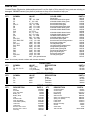
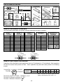
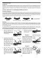
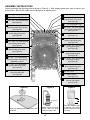
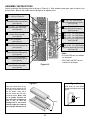
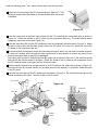
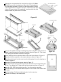
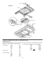
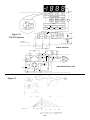
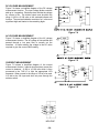
DIGITAL MULTIMETER KIT
MODEL M-1005K
Assembly and Instruction Manual
Elenco Electronics, Inc.
Copyright © 1996 Elenco Electronics, Inc.
REV-J
Revised 2000
753042
PARTS LIST
Contact Elenco Electronics (address/phone/e-mail is at the back of this manual) if any parts are missing or
damaged. DO NOT contact your place of purchase as they will not be able to help you.
RESISTORS
QTY
1
1
1
1
2
1
1
1
1
1
1
1
1
2
3
1
2
2
1
1
1
1
1
2
1
SYMBOL
VALUE
COLOR CODE
PART #
R0
R8
R7
R9
R10, R*
R6
R5
R13
R18
R11
R4
R12
R3
R16, R26
R2A, R2B, R2C
R15
R21, R22
R1A, R1B
R14
R25
R23
R24
R17
R19, R20
VR1
.01Ω
.99Ω .5% 1/4W
9Ω .5% 1/4W
10Ω 5% 1/4W
100Ω 5% 1/4W
100Ω .5% 1/4W
900Ω .5% 1/4W
900Ω 1% 1/4W
2kΩ PTC1
9kΩ 1% 1/4W
9kΩ .5% 1/4W
20kΩ 1% 1/4W
90kΩ .5% 1/4W
100kΩ 5% 1/4W
117kΩ 1% 1/4W
180kΩ 5% 1/4W
220kΩ 5% 1/4W
274kΩ 1% 1/4W
300kΩ 5% 1/4W
470kΩ 5% 1/4W
510kΩ 5% 1/4W
820kΩ 5% 1/4W
1.2MΩ 5% 1/4W
2.2MΩ 5% 1/4W
200Ω (201) potentiometer
Shunt Wire
black-white-white-silver-green
white-black-black-silver-green
brown-black-black-gold
brown-black-brown-gold
brown-black-black-black-green
white-black-black-black-green
white-black-black-black-brown
100160
109950
119000
121000
131000
131050
139050
139030
142069
149030
149050
152030
159050
161000
161130
161800
162200
162730
163000
164700
165100
168200
171200
172200
191310
white-black-black-brown-brown
white-black-black-brown-green
red-black-black-red-brown
white-black-black-red-green
brown-black-yellow-gold
brown-brown-violet-orange-brown
brown-gray-yellow-gold
red-red-yellow-gold
red-violet-yellow-orange-brown
orange-black-yellow-gold
yellow-violet-yellow-gold
green-brown-yellow-gold
gray-red-yellow-gold
brown-red-green-gold
red-red-green-gold
Note: Your kit may contain a resistor with a better tolerance.
CAPACITORS
QTY
1
4
1
SYMBOL
VALUE
DESCRIPTION
C1
C2, C3, C4, C6
C5
100pF (101)
.1µF (104)
.1µF (104/100n)
Disc
Mylar Small
Mylar Large
SYMBOL
VALUE
DESCRIPTION
D1
IC1
Q1
Q2
1N4007
7106
9013
9014
Diode
IC 40-Pin
Transistor
Transistor
PART #
221017
251018
251019
SEMICONDUCTORS
QTY
1
1
1
1
PART #
314007
337106
339013
339014
MISCELLANEOUS
QTY
2
1
1
1
1
1
1
1
1
1
1
2
2
2
DESCRIPTION
Zebra
PC Board
Fuse .25A 250V
Battery 9V
Battery Snap
LCD
Selector Knob
Case Top (Black)
Case Bottom (Black)
LCD Cover
LCD Frame
Screw 2.3mm x 6mm
Screw 2.3mm x 10mm
Fuse Clip
PART #
QTY
1
1
3
2
6
2
1
1
1
1
1
1
1
500003H
516100H
533003
590009
590098
621016H
622100H
623110H
623208H
621040H
629008H
643439E
643447E
663100E
-1-
DESCRIPTION
Socket Transistor
Socket 40-pin
Input Socket
Ball Bearing
Slide Contact
Spring 1/4” (Selector Knob)
Spring 1/2” (Shield)
Label Shield
Label Front
Manual Assembly
Grease
Solder Tube
Test Lead Set
PART #
664007
664040
664101H
666400E
680013E
680014E
680015E
723007H
724007H
753042
790004
9ST4
RWTL1000B
PARTS IDENTIFICATION
Battery Snap
Resistors
LCD Assembly
Zebras/LCD/Frame/Cover
Integrated Circuit
and Socket
Transistor
Test Socket
IC
Shunt Wire
PTC
Springs Potentiometer
Ball
Bearing
Fuse
Clip
Zebras
Slide
Contact
Fuse
Input Socket
LCD
Socket
Selector Knob
Capacitors
Transistor
Frame
Diode
C5
Cover
Mylar
Discap
IDENTIFYING RESISTOR VALUES
Use the following information as a guide in properly identifying the value of resistors.
BAND 1
1st Digit
Color
Black
Brown
Red
Orange
Yellow
Green
Blue
Violet
Gray
White
Digit
0
1
2
3
4
5
6
7
8
9
BAND 2
2nd Digit
Color
Black
Brown
Red
Orange
Yellow
Green
Blue
Violet
Gray
White
Digit
0
1
2
3
4
5
6
7
8
9
Color
Black
Brown
Red
Orange
Yellow
Green
Blue
Violet
Gray
White
Resistance
Tolerance
Color
Multiplier
Black
1
Brown
10
Red
100
Orange
1,000
Yellow
10,000
Green
100,000
Blue
1,000,000
Silver
0.01
Gold
0.1
Digit
0
1
2
3
4
5
6
7
8
9
Color
Silver
Gold
Brown
Red
Orange
Green
Blue
Violet
Tolerance
+10%
+5%
+1%
+2%
+3%
+.5%
+.25%
+.1%
5 Bands
4 Bands
1 2
Multiplier
BAND 3
(If Used)
1
Multiplier
2 3 Multiplier
Tolerance
Tolerance
IDENTIFYING CAPACITOR VALUES
Capacitors will be identified by their capacitance value in pF (picofarads) or µF (microfarads). Most capacitors
will have their actual value printed on them. Some capacitors may have their value printed in the following
manner.
Second Digit
First Digit
Multiplier
Tolerance
Multiplier
For the No.
0
1
2
3
Multiply By
1
10
100
1k
4
5
8
10k 100k .01
9
0.1
Note: The letter “R” may be used at times to
signify a decimal point; as in 3R3 = 3.3
The above value is 10 x 1,000 = 10,000pF or .01µF
The letter K indicates a tolerance of +10%
The letter J indicates a tolerance of +5%
-2-
CONSTRUCTION
Introduction
Assembly of your M-1005K Digital Multimeter Kit will prove to be an exciting project and give you much satisfaction and personal
achievement. If you have experience in soldering and wiring techniques, then you should have no problem with the assembly of this kit.
Care must be given to identifying the proper components and in good soldering habits. Above all, take your time and follow these easy
step-by-step instructions. Remember, “An ounce of prevention is worth a pound of cure”. Avoid making mistakes and no problems will
occur.
CAUTION: WEAR SAFETY GLASSES WHEN ASSEMBLING THIS KIT.
Assemble Components
In all of the following assembly steps, the components must be installed on the top side of the PC board unless otherwise indicated. The
top legend shows where each component goes. The leads pass through the corresponding holes and the board is turned to solder the
component leads on the foil side. Solder immediately unless the pad is adjacent to another hole which will interfere with the placement
of the other component. Cut excessive leads with a diagonal cutter. Then, place a check mark in the box provided next to each step to
indicate that the step is completed. Be sure to save the extra leads for use as jumper wires if needed.
Foil Side
Rx - 100Ω 5% 1/4W Resistor
(brown-black-brown-gold)
Mount Part
Bend Leads to Hold Part
Solder and Cut Off Leads
Soldering
The most important factor in assembling your digital multimeter is good soldering techniques. Using the proper soldering iron is of prime
importance. A small pencil type soldering iron of 25 - 40 watts is recommended. The tip of the iron must be kept clean at all times
and well tinned. Many areas on the PC board are close together and care must be given not to form solder shorts. Size and care of
the tip will eliminate problems.
For a good soldering job, the areas being soldered must be heated sufficiently so that the solder flows freely. Apply the solder
simultaneously to the component lead and the component pad on the PC board so that good solder flow will occur. Be sure that the
lead extends through the solder smoothly indicating a good solder joint. Use only rosin core solder of 60/40 alloy.
DO NOT USE ACID CORE SOLDER! Do not blob the solder over the lead because this can result in a cold solder joint.
1.
Solder all components from
the copper foil side only.
Push the soldering iron tip
against both the lead and the
circuit board foil.
Soldering Iron
4.
Component Lead
Foil
Here is what a good solder
connection looks like. Cut
off excess leads.
Example 1
Circuit Board
2.
3.
First apply a small amount of
solder to the iron tip. This
allows the heat to leave the
iron and onto the foil.
Immediately apply solder to
the opposite side of the
connection, away from the
iron.
Allow the heated
component and the circuit
foil to melt the solder.
Allow the solder to flow
around the connection.
Then, remove the solder and
the iron and let the
connection cool. The solder
should have flowed smoothly
and not lump around the wire
lead.
Poor solder connections occur
when the lead is not heated
sufficiently. The solder will not
flow onto the lead as shown. To
correct. reheat the connection
and, if necessary, apply a small
amount of additional solder to
obtain a good connection.
Soldering Iron
Solder
Foil
Example 2
Solder
Soldering Iron
Foil
-3-
A solder bridge occurs when
solder runs between circuit
paths and creates a short
circuit. This is usually caused
by using too much solder. To
correct this, simply drag your
soldering iron across the
solder bridge as shown.
Solder does not flow onto the
lead. A hard rosin bead
surrounds and insulates the
connection.
Poor solder
connection
Soldering iron
positioned incorrectly.
ASSEMBLY INSTRUCTIONS
Identify and install the following parts as shown in Figure 4-1. After soldering each part, mark a check in the
box provided. Be sure that solder has not bridged to an adjacent pad.
C3 - .1µF (104) Mylar Small
C4 - .1µF (104) Mylar Small
C2 - .1µF (104) Mylar Small
R14 - 300kΩ 5% 1/4W Resistor
(orange-black-yellow-gold)
(see Figure B)
VR1 - 200Ω (201) Potentiometer
(see Figure A)
C5 - .1µF (104) Mylar Large
R13 - 900Ω 1% 1/4W Resistor
(white-black-black-black-brown)
(see Figure B)
R23 - 510kΩ 5% 1/4W Resistor
(green-brown-yellow-gold)
(see Figure B)
R15 - 180kΩ 5% 1/4W Resistor
(brown-gray-yellow-gold)
(see Figure B)
Q2 - 9014 Transistor
(see Figure C)
R25 - 470kΩ 5% 1/4W Resistor
(yellow-violet-yellow-gold)
(see Figure B)
C1 - 100pF (101) Discap
R26 - 100kΩ 5% 1/4W Resistor
(brown-black-yellow-gold)
(see Figure B)
R20 - 2.2MΩ 5% 1/4W Resistor
(red-red-green-gold)
(see Figure B)
R16 - 100kΩ 5% 1/4W Resistor
(brown-black-yellow-gold)
(see Figure B)
C6 - .1µF (104) Mylar Small
R24 - 820kΩ 5% 1/4W Resistor
(gray-red-yellow-gold)
(see Figure B)
R8 - .99Ω .5% 1/4W Resistor
(black-white-white-silver-green)
(Standard Location)
R19 - 2.2MΩ 5% 1/4W Resistor
(red-red-green-gold)
(see Figure B)
R* - 100Ω 5% 1/4W Resistor
(brown-black-brown-gold)
(see Figure B)
R9 - 10Ω 5% 1/4W Resistor
(brown-black-black-gold)
(see Figure B)
R21 - 220kΩ 5% 1/4W Resistor
(red-red-yellow-gold)
(see Figure B)
R18 - 2kΩ PTC1
D1 - 1N4007 Diode
(see Figure E)
R22 - 220kΩ 5% 1/4W Resistor
(red-red-yellow-gold)
(see Figure B)
Figure A
Figure B
White Circle
Mount the potentiometer to the PC board
as shown.
Stand resistor on end as
shown with the body
inside the white circle
-4-
Figure C
1/8”
Mount the transistor with
the flat side in the same
direction marked on the
PC board.
ASSEMBLY INSTRUCTIONS
Identify and install the following parts as shown in Figure 4-2. After soldering each part, mark a check in the
box provided. Be sure that solder has not bridged to an adjacent pad.
IC - Socket 40-pin
IC - 7106 (see Figure D)
R11 - 9kΩ 1% 1/4W Resistor
(white-black-black-brown-brown)
(see Figure B)
R4 - 9kΩ .5% 1/4W Resistor
(white-black-black-brown-green)
(see Figure B)
R12 - 20kΩ 1% 1/4W Resistor
(red-black-black-red-brown)
(see Figure B)
R3 - 90kΩ .5% 1/4W Resistor
(white-black-black-red-green)
(see Figure B)
R17 - 1.2MΩ 5% 1/4W Resistor
(brown-red-green-gold)
(see Figure B)
R2A - 117kΩ 1% 1/4W Resistor
R2B - 117kΩ 1% 1/4W Resistor
R2C - 117kΩ 1% 1/4W Resistor
(brown-brown-violet-orange-brown)
(see Figure B)
Q1 - 9013 Transistor
(see Figure C)
R1A - 274kΩ 1% 1/4W Resistor
R1B - 274kΩ 1% 1/4W Resistor
(red-violet-yellow-orange-brown)
(see Figure B)
R6 - 100Ω .5% 1/4W Resistor
(brown-black-black-black-green)
(see Figure B)
R5 - 900Ω .5% 1/4W Resistor
(white-black-black-black-green)
(see Figure B)
* Note:
• R1A and R1B are not marked
on the board.
R7 - 9Ω .5% 1/4W Resistor
(white-black-black-silver-green)
(see Figure B)
• R2A, R2B, and R2C are not
marked on the board.
R10 - 100Ω 5% 1/4W Resistor
(brown-black-brown-gold)
(see Figure B)
Figure 4-2
Figure D
Figure E
Stand diode on end. Mount
with band as shown on the top
legend.
Align the socket notch (if any)
with the notch marked on the
PC board. Solder the socket to
the PC board. Insert the IC
into the socket with the notch
as shown below. Note: If the
IC is already inserted into
the socket, do not attempt to
pull it out, as this will
damage the IC and socket.
Instead, solder the socket to
the PC board with the IC in it.
Band
Notch
-5-
Install the following parts. Then, place a check mark in the box provided.
Solder the 1/2 inch spring to the PC board as shown in Figure 4-3. This
spring will contact the metal shield on the case bottom when the bottom
is installed.
Spring
Figure 4-3
Insert the narrow end of the three input sockets into the PC board from the component side, as shown in
Figure 4-4. Solder the sockets to the PC board on the components side only. The solder should extend
completely around the socket (see Figure 4-4).
Insert the shunt wire (R0) into the PC board holes from the component side as shown in Figure 4-4. Adjust
the wire so that it sticks out the other (solder) side of the PC board 3/16 of an inch. Solder the wire to the
PC board on the component side only.
Be sure that the 8 pin transistor socket will slide easily through its hole in the top case from either direction.
If it does not, carefully slide it through the hole several times in each direction to remove any burrs. Do not
push on the socket leads or they may be damaged.
Insert the socket into the PC board holes from the solder side as shown in Figure 4-4. Be sure that the tab
lines up with the hole as shown in the figure. Solder the socket to the PC board on the component side of
the PC board as shown in the figure and cut off excess leads.
Feed the battery snap wires up through the hole in the PC board from the solder side as shown in Figure 4-4.
Insert the red wire into the hole marked (V+) and black wire into hole marked (V--) as shown. Solder the wires
to the PC board.
Insert the two fuse clips into the PC board holes as shown in Figure 4-4. Be sure that the tabs are on the
outside as shown in the figure. Solder the clips to the PC board.
Input Sockets
Fuse Clips
Figure 4-4
Solder Side
Tab
Shunt Wire
Solder Side
Solder
Input
Socket
Battery Snap
Red Wire
Black Wire
Transistor
Socket
-6-
Close-up view of the
transistor socket and
PC board.
Remove the clear protective film from the front of the LCD (Note:
DO NOT remove the silver backing). Place the LCD and zebras in
the LCD frame as shown in Figure 4-5. Be sure that the LCD tab is
in the same direction as shown in the figure. Insert the square pins
of the LCD frame into the PC board holes, from the solder side, and
snap the frame into place on the PC board.
Clear Protective Film
Figure 4-5
Snap tab into place.
Zebras
PC Board
LCD
Square
Pins
Tab
1/4” Springs
Spring Holes
LCD Frame
Beveled Pins
Cut open the plastic envelope containing the grease and put a small amount of
grease in each spring hole of the selector knob as shown in Figure 4-6. Then, insert
a 1/4” spring into each hole as shown in the figure.
Figure 4-6
Put the bearings into two opposite indents in the case top as shown in Figure 4-7.
Place the six slide contactors on the selector knobs as shown in Figure 4-7.
Place the selector knob into the case top so that the springs fit over the bearings as
shown in Figure 4-7.
Place the LCD cover into the case as shown in Figure 4-7.
Place the PC board over the selector knob. Be sure that the 8-pin socket slides into
its hole. Then fasten the PC board with two 6mm screws as shown in Figure 4-7.
Insert the .25A, 250V fuse into the fuse clips. Your fuse may be unmarked.
Peel the backing off of the shield label and place it in the inside of the bottom case
as shown.
Peel the backing off of the front label and place it on the case top.
Connect a 9V battery to the battery snap.
-7-
Shield
6mm Screws
Figure 4-7
PC Board
Selector Knob
LCD Cover
Rib
Slide Contactor
Close-up View
Case Top
Bearings
Battery Compartment
TESTING, CALIBRATION, AND TROUBLESHOOTING
TESTING OF LCD
With no test leads connected to the meter, move the selector switch around the dial. You should obtain the following
readings. A (--) sign may also be present or blinking.
4) Ohms, Diode and hFE Ranges: B indicates blank.
200
1 B B.B
1) DCV Range:
200m
0 0.0
2000
1
BBB
2000m
000
20k
1
B.B B
20
0.0 0
200k
1
B B.B
200
0 0.0
2000k
1
B
BB
1000
000
Diode (
)
1BBB
2) ACV Range:
200
0 0.0
000
hFE
750
000
3) DCA,10A Ranges:
200µ
2000µ
20m
200m
10A
0 0.0
000
0.0 0
0 0.0
0.0 0
-8-
If any of these tests fail:
a) Check that the battery is good.
b) Check that IC1 is installed according to Figure 4-2 of the assembly instructions. Check for bent pins that do not extend
into the IC socket. Check for good contact between the leads of the IC and the pins of the socket.
c) Check the values of resistors R14, R15, R19, R20, R23 - R25.
d) Check the values of capacitors C1 - C5.
e) Check that Q2 is installed according to Figure 4-1 of the assembly instructions.
f) Check the PC board for solder bridges and bad solder connections.
g) Check that the slide contactors are seated correctly.
h) Check that the LCD and zebras are seated correctly.
CALIBRATION
Refer to the METER OPERATION section for test lead connections and measurement procedure.
A/D CONVERTER CALIBRATION
Turn the range selector switch to the 20V position and connect the test leads. Using another meter of known accuracy,
measure a DC voltage of less than 20 volts (such as a 9V battery). Calibrate the kit meter by measuring the same voltage
and adjusting VR1 until the kit meter reads the same as the accurate meter (do not use the kit meter to measure its own
battery). When the two meters agree, the kit meter is calibrated. Turn the knob to the OFF position and remove the voltage
source.
SHUNT WIRE CALIBRATION
To calibrate the shunt wire, you will need a 5 amp current source such as a
5V power supply and a 1 ohm, 25 watt resistor. If a 5 amp source is not
available, you can use a lower current (2 amps). If no supply is available, it is
not important to do this test. Set the range switch to the 10A position and
connect the test leads as shown in Figure 5-1. If the meter reads higher than
5A, resolder the shunt wire so that there is less wire between the 10A DC and
COM sockets.
If the meter reads low, resolder the shunt wire so that there is more wire
between the sockets.
10ADC
VΩMA
COM
Figure 5-1
If the calibration fails:
a) Check the PC board for solder bridges and bad solder connections.
b) Check that Q1 is installed according to Figure 4-2 of the assembly instructions.
c) Check the values of resistor R10 - R13, R26, and potentiometer VR1.
DC VOLTS TEST
1) If you have a variable power supply, set the supply to about the midpoint of each of the DCV ranges and compare the
kit meter reading to a meter known accuracy.
2) If you do not have a variable power supply, make the following two tests:
a) Set the range switch to 2000mV and measure the voltage across the 100 ohm resistor of Figure 5-2A. You should
get about 820mV. Compare the reading to a meter of known accuracy.
b) Set the range switch to 200mV and measure the voltage across the 100 ohm resistor of Figure 5-2B. You should
get about 90mV. Compare the reading to a meter of known accuracy.
If any of these tests fail:
a) Recheck the meter calibration.
b) Check the value and the soldering
of resistors R1-R6, R16.
Figure 5-2B
10ADC
10ADC
Figure 5-2A
VΩMA
10k ohm
1k ohm
VΩMA
COM
COM
-9-
AC VOLTS TEST
To test the ACV ranges, we will need a source of AC voltage. The AC power line is the most convenient.
CAUTION: Be very careful when working with 120VAC. Be sure that the range switch is in the 200 or 750VAC
position before connecting the test leads to 120VAC.
1) Set the range to 200VAC and measure the AC power line. The voltage should be about 120VAC. Compare
the reading to a meter of known accuracy.
2) Set the range to 750VAC and measure the AC power line. The voltage should be about 120VAC. Compare
the reading to a meter of known accuracy.
If either if the above tests fail:
a) Check the values and the soldering of resistors R1 - R6, R16.
b) Check that diode D1 is mounted as shown in the assembly instructions.
DC AMPS TEST
1) Set the range switch to 200µA and connect the meter as in Figure 5-3. With RA equal to 100kΩ the current
should be about 90µA. Compare the reading to a known accurate meter.
2) Set the range switch and RA as in the following table. Read the currents shown and compare to a known
accurate meter.
RANGE SWITCH
2000µA
20mA
200mA
RA
10kΩ
1kΩ
470Ω
CURRENT (approx.)
900µA
9mA
19mA
If any of the above tests fail:
a) Check the fuse.
b) Check the value and soldering of resistors R7, R8, and R*.
10ADC
VΩMA
COM
Figure 5-3
RESISTANCE/DIODE TEST
1) Measure a resistor of about half of the full scale value of each resistance range. Compare the kit meter
readings to those from a meter of known accuracy.
2) Measure the voltage drop of a good silicon diode. You should read about 700mV. Power diodes and the
base to emitter junction of power transistors may read less.
If any of these tests fail:
a) Check the values and the soldering of resistors R1 - R6, and R18.
b) Check that transistor Q1 is mounted as shown in the assembly instructions.
hFE
1) Set the range switch to hFE and insert a small transistor into the appropriate NPN or PNP holes in the
transistor socket.
2) Read the hFE of the transistor. The hFE of transistors varies over a wide range, but you will probably get a
reading between 100 and 300.
If this check fails:
a) Check that the transistor socket is aligned according to Figure 4-4.
b) Check the value and soldering of resistors R9, R21, and R22
-10-
FINAL ASSEMBLY
Snap the case bottom onto the case top and fasten with the two 10mm screws as shown in Figure 6-1.
Screws
Figure 6-1
Case
Bottom
Battery
Case Top
THEORY OF OPERATION
A block diagram of the M-1005K is shown in Figure 7-1. Operation centers around a custom LSI chip. This chip
contains a dual slope A/D (analog to digital) converter, display latches, seven segment decoder and display
drivers. A block diagram of the IC functions is shown in Figure 7-2. The input voltage or current signals are
conditioned by the selector switches to produce an output DC voltage with a magnitude between 0 and 199mV.
If the input signal is 100VDC, it is reduced to 100mVDC by selecting a 1000:1 divider. Should the input be
100VAC, it is first rectified and then divided down to 100mVDC. If current is to be read, it is converted to a DC
voltage by internal shunt resistors.
Figure 7-1
-11-
For resistance measurements, an internal voltage source drives the test resistor in series with a known resistor.
The ratio of the test resistor voltage to the known resistor voltage is used to determine the value of the test
resistor.
The input of the 7106 IC is fed to an A/D converter. Here the DC voltage is changed to a digital format. The
resulting signals are processed in the decoders to light the appropriate LCD segments.
Timing for the overall operation of the A/D converter is derived from an external oscillator whose frequency is
selected to be 25kHz. In the IC, this frequency is divided by four before it clocks the decade counters. It is then
further divided to form the three convert-cycles phases. The final readout is clocked at about two readings per
second.
The digitized measurements are presented to the display as four decoded digits (seven segments) plus polarity.
The decimal point position on the display is determined by the selector switch setting.
A/D CONVERTER
A simplified circuit diagram of the analog portion of the A/D converter is shown in Figure 7-3. Each of the
switches shown represent analog gates which are operated by the digital section of the A/D converter. The
basic timing for switch operation is keyed by the external oscillator. The conversion process is continuously
repeated. A complete cycle is shown in Figure 7-3.
Any given measurement cycle performed by the A/D converter can be divided into three consecutive time
periods, autozero (AZ), integrate (INTEG) and read. A counter determines the length of the time periods. The
integrate period is fixed at 1000 clock pulses. The read period is a variable time that is proportional to the
unknown input voltage. It can vary from zero counts for zero input voltage to 2000 counts for a full scale input
voltage. The autozero period varies from 1000 to 3000 counts. For an input voltage less than full scale autozero
gets the unused portion of the read period. The value of the voltage is determined by counting the number of
clock pulses that occur during the read period.
During autozero a ground reference is applied as an input to the A/D converter. Under ideal conditions, the
output of the comparator would also go to zero. However, input-offset-voltage errors accumulate in the amplifier
loop and appear at the comparator output as an error voltage. This error is impressed across the AZ capacitor
where it is stored for the remainder of the measurement cycle. The stored level is used to provide offset voltage
correction during the integrate and read periods.
The integrate period begins at the end of the autozero period. As the period begins, the AZ switch opens and
the INTEG switch closes. This applies the unknown input voltage to the input of the A/D converter. The voltage
is buffered and passed on to the integrator to determine the charge rate (slope) on the INTEG capacitor At the
end of the fixed integrate period, the capacitor is charged to a level proportional to the unknown input voltage.
During the read period, this voltage is translated to a digital indication by discharging the capacitor at a fixed
rate and counting the number of clock pulses that occur before it returns to the original autozero level.
As the read period begins, the INTEG switch opens and the read switch closes. This applies a known reference
voltage to the input to the A/D converter. The polarity of this voltage is automatically selected to be opposite
that of the unknown input voltage, thus causing the INTEG capacitor to discharge at a fixed rate (slope). This
rate is determined by the known reference voltage. When the charge is equal to the initial starting point
(autozero level), the read period is ended. Since the discharge slope is fixed during the read period, the time
required for discharge is proportional to the unknown input voltage. Specifically, the digital reading displayed is
1000 (VIN / VREF).
The autozero period and thus a new measurement cycle begins at the end of the read period. At the same time
the counter is released for operation by transferring its contents (the previous measurement value) to a series of
latches. This stored data is then decoded and buffered before being used to drive the LCD display.
-12-
a
f
a
b
g
b
e
c
d
BACKPLANE
21
LCD PHASE DRIVER
7 Segment
Decode
7 Segment
Decode
TYPICAL SEGMENT OUTPUT
V+
7 Segment
Decode
200
0.5mA
LATCH
Segment
Output
2mA
Thousand
Tens
Hundreds
Units
Internal Digital Ground
To Switch Drivers
From Comparator Output
V+
CLOCK
Figure 7-2
7106 IC Functions
6.2V
LOGIC CONTROL
-4
*
37
TEST
Internal Digital Ground
1V
500Ω
* Three inverters.
One inverter shown for clarity.
26
40
39
OSC 3
OSC 2
OSC 1
CREF
CREF+
REF HI
34
V+
A-Z &
Z1
35
33
A-Z &
Z1
Z1
31
IN LO
30
INT
29
6.2V
INT
INTEGRATOR
27
+
+
A-Z
COMPARATOR
ZERO
CROSSING
DETECTOR
POLARITY
FLIP/FLOP
TO
DIGITAL
SECTION
+
DE (+)
32
1
CINT
DE (+)
A-Z
COMMON
28
2.8V
DE (-)
CAZ
AUTO
ZERO
V+
+
10µA
INT
IN HI
DIGITAL SECTION
RINT
REF LO CREF BUFFER
36
V
38
ANALOG SECTION of 7106
DE (-)
A-Z & DE(+)
& Z1
26
V
Figure 7-3
-13-
DC VOLTAGE MEASUREMENT
Figure 7-4 shows a simplified diagram of the DC voltage
measurement function. The input voltage divider resistors
add up to 1 megaohm. Each step down divides the voltage
by a factor of ten. The divider output must be within the
range -0.199 to +0.199 volts or the overload indicator will
function. The overload indication consists of a 1 in the most
significant digit and blanks in the remaining digits.
Figure 7-4
AC VOLTAGE MEASUREMENT
Figure 7-5 shows a simplified diagram of the AC voltage
measurement function. The AC voltage is first rectified and
passed through a low pass filter to smooth out the
waveform. A scaler reduces the voltage to the DC value
required to give the correct RMS reading.
Figure 7-5
CURRENT MEASUREMENT
Figure 7-6 shows a simplified diagram of the current
measurement function. Internal shunt resistors convert the
current to between -0.199 to +0.199 volts which is then
processed in the 7106 IC to light the appropriate LCD
segments. When current in the range of 10A is to be read,
it is fed to the 10A input and does not pass through the
selector switch.
Figure 7-6
e
b
c
e
e
b
c
e
NPN PNP
-14-
RESISTANCE MEASUREMENT
Figure 7-7 shows a simplified diagram of the resistance measurement
function. A simple series circuit is formed by the voltage source, a
reference resistor from the voltage divider (selected by the selector
switches), and the test (unknown) resistor. The ratio of the two resistors
is equal to the ratio of their respective voltage drops. Therefore, since
the value of one resistor is known, the value of the second can be
determined by using the voltage drop across the known resistor as a
reference. This determination is made directly by the A/D converter.
Overall operation of the A/D converter during a resistance
measurement is basically as described earlier with one exception. The
reference voltage present during a voltage measurement is replaced by
the voltage drop across the reference resistor. This allows the voltage
across the unknown resistor to be read during the read period.
Figure 7-7
hFE MEASUREMENT
Figure 7-8 shows a simplified diagram of the hFE measurement function.
Internal circuits in the 7106 IC maintain the COMMON line at 2.8 volts
below V+. When a PNP transistor is plugged into the transistor socket,
base to emitter current flows through resistor R21. The voltage drop in
resistor R10 due to the collector current is fed to the 7106 and indicates
the hFE of the transistor. For an NPN transistor, the emitter current
through R10 indicates the hFE of the transistor.
Figure 7-8
SPECIFICATIONS
GENERAL
DC CURRENT
DISPLAY
OVERRANGE INDICATION
MAXIMUM COMMON MODE
VOLTAGE
STORAGE ENVIRONMENT
TEMPERATURE COEFFICIENT
POWER
DIMENSIONS
3 1/2 digit LCD, with polarity
3 least significant digits blanked.
RANGE
200µA
2000µA
20mA
200mA
10A
500V peak.
-15oC to 50oC.
(0oC to 18oC and 28oC to 50oC) less
than 0.1 x applicable accuracy
specification per oC.
9V alkaline or carbon zinc battery.
128 x 75 x 24mm.
OVERLOAD PROTECTION
RESOLUTION
0.1mV
1mV
10mV
100mV
1V
MAXIMUM ALLOWABLE INPUT
INPUT IMPEDANCE
ACCURACY
+1% rdg + 2d
+1% rdg + 2d
+1% rdg + 2d
+1.2% rdg + 2d
+2% rdg + 3d
.25A/250V fuse (mA input only).
AC VOLTAGE
RANGE
200V
750V
DC VOLTAGE
RANGE
200mV
2000mV
20V
200V
1000V
RESOLUTION
0.1µA
1µA
10µA
100µA
10mA
ACCURACY
+0.5% rdg + 2d
+0.5% rdg + 2d
+0.5% rdg + 2d
+0.5% rdg + 2d
+0.5% rdg + 2d
RESOLUTION
100mV
1V
ACCURACY
+1.2% rdg + 10d
+1.2% rdg + 10d
MAXIMUM ALLOWABLE INPUT
FREQUENCY
750Vrms.
45 - 450Hz.
RESISTANCE
RANGE
200Ω
2000Ω
20kΩ
200kΩ
2000kΩ
1000VDC or peak AC.
1MΩ.
RESOLUTION
0.1Ω
1Ω
10Ω
100Ω
1kΩ
ACCURACY
+0.8% rdg + 2d
+0.8% rdg + 2d
+0.8% rdg + 2d
+0.8% rdg + 2d
+1% rdg + 2d
MAXIMUM OPEN CIRCUIT VOLTAGE
2.8V.
DIODE CHECK
RANGE
DIODE
RESOLUTION
1mV
MAX TEST CURRENT
1.4mA
MAX OPEN CIRCUIT VOLTAGE
2.8V
TEST RANGE
0 - 1000
TEST CURRENT
Ib = 10µA
TEST VOLTAGE
Vce 3V
TRANSISTOR hFE TEST
RANGE
NPN/PNP
-15-
METER OPERATION
PRECAUTIONS AND PREPARATIONS FOR MEASUREMENT
1) Be sure the battery is connected to the battery snap and correctly placed in the battery compartment.
2) Before connecting the test leads to the circuit, be sure the range switch is set to the correct position.
3) Be sure that the test leads are connected to the correct meter terminals before connecting them to the
circuit.
4) Before changing the range switch, remove one of the test leads from the circuit.
5) Operate the instrument only in temperatures between 0 and 50OC and in less than 80% RH.
6) Pay careful attention to the maximum rated voltage of each range and terminal.
7) When finished making measurements, set the switch to OFF. Remove the battery when the instrument will
not be used for a long period of time.
8) Do not use or store the instrument in direct sunlight or at high temperature or humidity.
VOLTAGE MEASUREMENTS
1) Connect the black test lead to the “COM” terminal.
2) Connect the red test lead to the “VΩMA” terminal.
3) Set the range switch to the desired “V
the switch to the highest range.
” or “V~” position. If the magnitude of the voltage is not known, set
4) Connect the leads across the points to be measured and read the display. If the range switch is too high,
reduce it until a satisfactory reading is obtained.
DCA MEASUREMENTS
HIGH CURRENTS (200mA to 10A)
1) Connect the black test lead to the “COM” terminal.
2) Connect the red test lead to the 10ADC terminal.
3) Set the range switch to the 10A
position.
4) Open the circuit to be measured and connect the leads in series with the load to be measured.
5) Read the display. If the display read less than 200mA, follow the low current procedure below.
6) Turn off all of the power to the circuit being tested and discharge all of the capacitors before disconnecting
the test leads.
LOW CURRENTS (less than 200mA)
7) Connect the black test lead to the “COM” terminal.
8) Connect the red test lead to the VΩMA terminal.
9) Set the range switch to the desired A position. If the magnitude of the current is not known, set the switch
to the highest position.
10) Open the circuit to be measured and connect the leads in series with the load to be measured.
11) Read the display. If the range switch is too high, reduce it until a satisfactory reading is obtained.
12) Turn off all power to the circuit being tested and discharge all capacitors before disconnecting the test leads.
-16-
RESISTANCE MEASUREMENTS
1)
2)
3)
4)
Connect the black test lead to the “COM” terminal.
Connect the red test lead to the “VΩMA” terminal.
Set the range switch to the desired “Ω” position.
If the resistance being measured is connected to a circuit, turn off the power to the circuit being tested and
discharge all of the capacitors.
5) Connect the leads across the resistor to be measured and read the display. When measuring high
resistance, be sure not to contact adjacent points even if insulated. Some insulators have relatively low
resistance and will cause the measured resistance to be lower than the actual resistance.
DIODE CHECK
1) Connect the black test lead to the “COM” terminal.
2) Connect the red test lead to the “VΩMA” terminal.
3) If the diode being measured is connected to a circuit, turn off all power to the circuit and discharge all
capacitors.
4) Set the range switch to “
”.
Forward Voltage Check
5) Connect the red lead to the anode and the black lead to the cathode of the diode. Normally the forward
voltage drop of a good silicon diode reads between 450 and 900mV.
Reverse Voltage Check
6) Reverse the leads to the diode. If the diode is good, an overrange indication is given (a 1 in the most
significant digit and blanks in the remaining digits). If the diode is bad, “000” or some other value is
displayed.
hFE MEASUREMENTS
1) Set the range switch to hFE and insert the test transistor into the appropriate NPN or
PNP holes in the transistor socket.
2) Read the hFE of the transistor.
BATTERY & FUSE REPLACEMENT
If “ + ” appears on the display, it indicates that the battery should be replaced.
To replace battery and fuse (250mA/250V), remove the 2 screws in the bottom of the case.
Simply remove the old fuse/battery and replace with a new fuse/battery.
QUIZ
1. The function of the A/D converter is to . . .
A) convert digital to analog.
B) divide the analog signal by 2.
C) convert analog to digital.
D) convert AC to DC.
2. The divider used for DC voltage measurements is a . . .
A) divide by 20.
B) capacitance divider.
C) divide by 5.
D) resistor divider.
3. When the AC voltage is measured, it is first . . .
A) divided by 2.
B) rectified.
C) divided by 100.
D) sent to a high pass filter.
4. When measuring current, the shunt resistors convert the
current to . . .
A) -0.199 to +0.199 volts.
B) -1.199 to +1.199 volts.
C) -0.099 to +0.099 volts.
D) -199 to +199 volts.
5. The DC voltage divider resistors add up to . . .
A) 100Ω.
B) 1000Ω.
C) 100kΩ.
D) 1MΩ.
e
b
c
e
e
b
c
e
NPN PNP
6. Resistance measurements are made by . . .
A) comparing voltage drops in the unknown resistor and a
reference resistor.
B) measuring the current in the unknown resistor.
C) measuring the current in the reference resistor.
D) equalizing the voltage drops in the unknown and the
reference resistors.
7. The measurement cycle performed by the A/D converter can be
divided into time periods known as . . .
A) long and short.
B) autozero, integrate and read.
C) zero, read and interphase.
D) convert, integrate and display.
8. A resistor with the band colors green-black-green-brown-green is . . .
A) 50.5kΩ +5%.
B) 5.15kΩ +10%.
C) 5.05kΩ +.5%.
D) 5.05kΩ +1%.
9. The M-1005K has . . .
A) A 3 digit display.
B) A 3 1/2 digit display.
C) A 4 1/2 digit display.
D) None of the above.
10.When measuring 450mA, the meter leads should be connected to . . .
A) COM and VΩmA.
B) COM and 10A.
C) 10A and VΩmA.
D) COM and Building GND.
-17-
Answers: 1. C, 2. D, 3. B, 4. A,
5. D, 6. A, 7. B, 8. C, 9. B, 10. B
TEST
REF HI
INPUT LO
AUTO-ZERO
BUFFER
(--) SUPPLY
G (TENS)
C (100’s)
G (100’s)
BACKPLANE
36
32
31
30
29
28
27
26
25
24
23
22
21
5
6
7
8
9
A (UNITS)
F (UNITS)
G (UNITS)
E (UNITS)
D (TENS)
C (TENS) 10
B (TENS) 11
A (TENS) 12
F (TENS) 13
E (TENS) 14
D (100’s) 15
B (100’s) 16
F (100’s) 17
E (100’s) 18
AB (1000) 19
POLARITY 20
(MINUS)
7106
OSC 3
37
4
B (UNITS)
-- REF CAP
34
33
A (100’s)
INTEGRATOR
INPUT HI
COMMON
REF LO
+ REF CAP
35
OSC 2
38
3
OSC 1
C (UNITS)
40
D (UNITS)
39
1
2
(+) SUPPLY
SCHEMATIC DIAGRAM
-18-
Elenco Electronics, Inc.
150 W. Carpenter Avenue
Wheeling, IL 60090
(847) 541-3800
www.elenco.com
e-mail: [email protected]