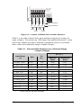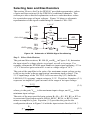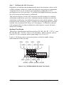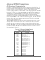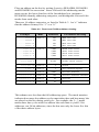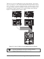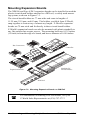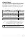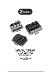
1
XP8 500 Exp -A/D 12 XP8500 and Exp-A/D12 Analog-to-Digital Conversion Expansion Boards Users Manual Revision B XP8500 and Exp-A/D12 Users Manual Part Number 019-0055 Revision B Last revised on April 9, 1999 Printed in U.S.A. Copyright © 1999 Z-World All rights reserved. Z-World reserves the right to make changes and improvements to its products without providing notice. Trademarks ® Dynamic C is a registered trademark of Z-World ® Windows is a registered trademark of Microsoft Corporation PLCBus is a trademark of Z-World ® Hayes Smart Modem is a registered trademark of Hayes Microcomputer Products, Inc. Notice to Users When a system failure may cause serious consequences, protecting life and property against such consequences with a backup system or safety device is essential. The buyer agrees that protection against consequences resulting from system failure is the buyers responsibility. This device is not approved for life-support or medical systems. All Z-World products are 100 percent functionally tested. Additional testing may include visual quality control inspections or mechanical defects analyzer inspections. Specifications are based on characterization of tested sample units rather than testing over temperature and voltage of each unit. Z-World may qualify components to operate within a range of parameters that is different from the manufacturers recommended range. This strategy is believed to be more economical and effective. Additional testing or burn-in of an individual unit is available by special arrangement. Company Address Z-World 2900 Spafford Street Davis, California 95616-6800 USA Telephone: Facsimile: Web Site: E-Mail: (530) 757-3737 (530) 753-5141 http://www.z w orld.com [email protected] TABLE OF CONTENTS About This Manual vii XP8500 Chapter 1: Overview 13 Chapter 2: Getting Started 15 Chapter 3: I/O Configurations 19 Chapter 4: Software Reference 33 XP8500 Components ........................................................................... 16 Connecting Expansion Boards to a Z-World Controller ...................... 17 Setting Expansion Board Addresses .................................................... 18 XP8500 Addresses .......................................................................... 18 Power ................................................................................................... 18 XP8500 Pin Assignments ..................................................................... 20 Operating Modes ................................................................................. 20 Using Analog-to-Digital Converter Boards ......................................... 21 How to Set Up An XP8500 .................................................................. 22 Conditioned Inputs (CH0CH3) ..................................................... 22 Excitation Resistors ...................................................................... 24 EEPROM ...................................................................................... 24 Unconditioned Inputs (AIN4AIN10) ............................................ 25 Internal Test Voltages ...................................................................... 25 Power-Down Mode ......................................................................... 25 Drift ................................................................................................. 26 Selecting Gain and Bias Resistors ....................................................... 27 Expansion Board Addresses ................................................................ 34 XP8500 Software ................................................................................. 35 Dynamic C Libraries ....................................................................... 35 Initialization Software ..................................................................... 36 XP8500 Drivers .............................................................................. 37 Other XP8500 Drivers .................................................................. 39 Correcting Readings ..................................................................... 44 Sample Program .............................................................................. 44 Advanced XP8500 Programming ........................................................ 47 PLCBus-Level Communication ...................................................... 47 XP8500 and Exp-A/D12 Contents s iii Exp-A/D12 Chapter 5: Overview 51 Chapter 6: Getting Started 53 Chapter 7: I/O Configurations 59 Chapter 8: Software Reference 65 Exp-A/D12 Components ...................................................................... 54 Connecting Expansion Boards to a Z-World Controller ...................... 55 Setting Expansion Board Addresses .................................................... 56 Exp-A/D12 Addresses ..................................................................... 56 Power ................................................................................................... 56 Exp-A/D12 Pin Assignments ............................................................... 60 Using Analog-to-Digital Converter Boards ......................................... 60 How to Set Up An Exp-A/D12 ............................................................ 61 The Multiplexers ............................................................................. 62 The Op-Amps .................................................................................. 62 The A/D Converter .......................................................................... 63 Expansion Board Addresses ................................................................ 66 Logical Addresses ........................................................................... 66 Exp-A/D12 Software ........................................................................... 67 The Signal Table ............................................................................. 67 Constants and Data Types ............................................................... 67 A/D Conversion Modes .................................................................. 68 General Exp-A/D12 Functions ........................................................ 69 A/D Conversion .............................................................................. 69 Accessing EEPROM ....................................................................... 70 Sample Program .............................................................................. 71 iv s Contents XP8500 and Exp-A/D12 APPENDICES Appendix A: PLCBus 75 Appendix B: Specifications 87 Appendix C: Connecting and Mounting Multiple Boards 93 Appendix D: Simulated PLCBus Connection 97 Appendix E: Technical Circuit Details 99 PLCBus Overview ............................................................................... 76 Allocation of Devices on the Bus ........................................................ 80 4-Bit Devices .................................................................................. 80 8-Bit Devices .................................................................................. 81 Expansion Bus Software ...................................................................... 81 XP8500 Hardware Specifications ........................................................ 88 Exp-A/D12 Hardware Specifications .................................................. 90 Connecting Multiple Boards ................................................................ 94 Mounting Expansion Boards ................................................................ 96 BL1400 and BL1500 ........................................................................... 98 XP8500 .............................................................................................. 100 Voltage Reference ......................................................................... 100 Conversion Modes ........................................................................ 100 Data Conversion ............................................................................ 101 Limitations on Output Range ........................................................ 101 Exp-A/D12 ......................................................................................... 102 Input Stability ................................................................................ 102 Effects of the OP6300 on Stability ................................................ 102 Multiplexer Settling Time ............................................................. 102 Index XP8500 105 and Exp-A/D12 Contents s v Blank vi s Contents XP8500 and Exp-A/D12 ABOUT THIS MANUAL This manual provides instructions for installing, testing, configuring, and interconnecting the Z-World XP8500 and Exp-A/D12 analog-to-digital conversion expansion boards. Instructions are also provided for using Dynamic C functions. Assumptions Assumptions are made regarding the user's knowledge and experience in the following areas: Ability to design and engineer the target system that is controlled by a controller with analog-to-digital conversion expansion boards. Understanding of the basics of operating a software program and editing files under Windows on a PC. Knowledge of the basics of C programming. $ The C Programming Language by Kernighan and Ritchie C: A Reference Manual by Harbison and Steel Knowledge of basic Z80 assembly language and architecture for controllers with a Z180 microprocessor. $ For a full treatment of C, refer to the following texts. For documentation from Zilog, refer to the following texts. Z180 MPU User's Manual Z180 Serial Communication Controllers Z80 Microprocessor Family User's Manual Knowledge of basic Intel assembly language and architecture for controllers with an Intel386 EX processor. $ XP8500 and For documentation from Intel, refer to the following texts. Intel386 EX Embedded Microprocessor Users Manual Intel386 SX Microprocessor Programmers Reference Manual Exp-A/D12 About This Manual s vii Acronyms Table 1 lists and defines the acronyms that may be used in this manual. Table 1. Acronyms Acronym Meaning EPROM Erasable Programmable Read-Only Memory EEPROM Electronically Erasable Programmable Read-Only Memory LCD Liquid Crystal Display LED Light-Emitting Diode NMI Nonmaskable Interrupt PIO Parallel Input/Output Circuit (Individually Programmable Input/Output) PRT Programmable Reload Timer RAM Random Access Memory RTC Real-Time Clock SIB Serial Interface Board SRAM Static Random Access Memory UART Universal Asynchronous Receiver Transmitter Icons Table 2 displays and defines icons that may be used in this manual. Table 2. Icons Icon $ ( Meaning Refer to or see ! Please contact Caution )' Icon Meaning Note High Voltage 7LS Tip Factory Default viii s About This Manual XP8500 and Exp-A/D12 Conventions Table 3 lists and defines the typographical conventions that may be used in this manual. Table 3. Typographical Conventions Example Description while Courier font (bold) indicates a program, a fragment of a program, or a Dynamic C keyword or phrase. // IN-01… Program comments are written in Courier font, plain face. Italics Indicates that something should be typed instead of the italicized words (e.g., in place of filename, type a file’s name). Edit Sans serif font (bold) signifies a menu or menu selection. ... An ellipsis indicates that (1) irrelevant program text is omitted for brevity or that (2) preceding program text may be repeated indefinitely. [ ] Brackets in a C function’s definition or program segment indicate that the enclosed directive is optional. ‹ › Angle brackets occasionally enclose classes of terms. a | b | c A vertical bar indicates that a choice should be made from among the items listed. Pin Number 1 A black square indicates pin 1 of all headers. Pin 1 J1 Measurements All diagram and graphic measurements are in inches followed by millimeters enclosed in parenthesis. XP8500 and Exp-A/D12 About This Manual s ix Blank x s About This Manual XP8500 and Exp-A/D12 XP8500 Blank CHAPTER 1: OVERVIEW Chapter 1 provides an overview and description of the XP8500 analog-todigital conversion expansion boards. XP8500 Overview s 13 The XP8500 provides 11 channels of 12-bit analog-to-digital (A/D) conversion, with onboard signal conditioning for four of these channels to match the input voltage range between 0 V and 10 V. Gain and bias resistors may be selected and installed by the user to determine the voltage ranges of the conditioned input signals. The XP8500 may be operated either in a ratiometric mode (a mode that reduces errors arising from power-supply variations) or in an absolute mode (where an onboard precision voltage reference assures accurate measurements). The printed circuit board has space for optional sensorexcitation resistors. Each XP8500 has its zero offset and gain for the four conditioned channels stored in an onboard, serial EEPROM. An application can use library functions to access the EEPROMs calibration constants to correct measurements for offset and gain error. The XP8500 receives its power from the PLCBus +24 V and +5 V. An onboard voltage regulator develops a clean +5 V supply for the boards analog circuitry from the +24 V PLCBus. The same version of the XP8500 works with both +12 V and +24 V controllers. Like other Z-World expansion boards, the XP8500 boards can be installed in modular plastic circuit-board holders attached to a DIN rail. The XP8500 boards can also be mounted, with plastic standoffs, on any surface that will accept screws. Up to 16 XP8500 boards addresses are possible on a single PLCBus. ( For ordering information, call your Z-World Sales Representative at (530) 757-3737. 14 s Overview XP8500 CHAPTER 2: GETTING STARTED Chapter 2 provides instructions for connecting XP8500 expansion boards to a Z-World controller. The following sections are included. XP8500 Components Connecting Expansion Boards to a Z-World Controller Setting Expansion Board Addresses Power XP8500 Getting Started s 15 XP8500 Components The XP8500 boards offer eleven channels of 12-bit analog-to-digital conversion. Figure 2-1 illustrates the basic layout and orientation of components, headers, and connectors. Regulator J5 J4 U8 U9 J3 C11 U7 PAL U6 U5 H2 P1 P2 U3 U2 RP4 U1 RP3 Gain and Bias Resistors H1 J2 J1 Figure 2-1. XP8500 Board Layout 16 s Getting Started XP8500 Connecting Expansion Boards to a Z-World Controller Use the 26-conductor ribbon cable supplied with an expansion board to connect the expansion board to the PLCBus on a Z-World controller. See Figure 2-2. The expansion boards two 26-pin PLCBus connectors, P1 and P2, are used with the ribbon cable. Z-World recommends using the cable supplied to avoid any connection problems. Controller PLCBus Port U8 U9 C11 J3 U7 PAL Pin 1 U6 U5 P1 H2 1 U3 U2 U1 P2 H1 XP8500 Controller With PLCBus Figure 2-2. Connecting XP8500 Expansion Board to Controller PLCBus Be sure power to the controller is disconnected before adding any expansion board to the PLCBus. Follow these steps to connect an expansion board to a Z-World controller. 1. Attach the 26-pin ribbon cable to the expansion boards P2 PLCBus header. 2. Connect the other end of the ribbon cable to the PLCBus port of the controller. Be sure pin 1 of the connector cable matches up with pin 1 of both the controller and the expansion board(s). 3. If additional expansion boards are to be added, connect header P2 on the new board to header P1 of the board that is already connected. Lay the expansion boards side by side with headers P1/H1 and P2/H2 on adjacent boards close together, and make sure that all expansion boards are facing right side up. $ XP8500 See Appendix C, Connecting and Mounting Multiple Boards, for more information on connecting multiple expansion boards. Getting Started s 17 4. Each expansion board comes with a factory-default board address. If more than one expansion board of each type is to be used, be sure to set a unique address for each board. $ The following section on Setting Expansion Board Addresses, and Chapter 4, Software Reference, provide details on how to set and use expansion board addresses. 5. Power may be applied to the controller once the controller and the expansion boards are properly connected using the PLCBus ribbon cable. $ See Appendix D, Simulated PLCBus Connection, for details on the special connections that enable XP8500 expansion boards to be used with BL1400 and BL1500 controllers. Setting Expansion Board Addresses Z-World has established an addressing scheme for the PLCBus on its controllers to allow multiple expansion boards to be connected to a controller. ! Remember that each expansion board must have a unique PLCBus address if multiple boards are to be connected. If two boards have the same address, communication problems will occur that may go undetected by the controller. XP8500 Addresses XP8600 expansion boards are shipped from the factory with no pins on header J4 or J5 connected. Four different PALs are available. There are four different ways to configure the pair of pins on header J4 and J5, and so up to 16 XP8500s may be addressed individually over a single PLCBus. $ See Chapter 4, Software Reference, for further details on how to determine the physical address for XP8500 expansion boards based on whether the pins on header J4 or header J5 are connected. Power Z-Worlds expansion boards receive power from the controller over the +24 V line of the PLCBus. An onboard regulator converts this to the +5 V reference used by the XP8500. The XP8500 draws 32 mA at +24 V. The XP8500 may be used with +12 V controllers without having any modifications. 18 s Getting Started XP8500 CHAPTER 3: I/O CONFIGURATIONS Chapter 3 describes the built-in flexibility of the XP8500 expansion boards, and describes how to configure the available inputs/outputs. The following sections are included. XP8500 Pin Assignments Operating Modes Using A/D Converter Boards How to Set Up an XP8500 Selecting Gain and Bias Resistors XP8500 I/O Configurations s 19 XP8500 Pin Assignments The XP8500s eleven 12-bit analog-to-digital converter channels are accessed through Wago connector H1 (conditioned channels CH0CH3) and header H2 (unconditioned channels AIN4AIN10), as shown in Figure 3-1. The bias voltage set by J1, VREF+, is available on header H2, and +5 V (analog) is available on both Wago connector H1 and header H2. CH0 GND CH3 +5ANA GND CH1 CH2 GND GND 1 2 AIN10 GND 3 GND 5 4 AIN9 6 AIN8 GND 7 8 AIN7 GND 9 10 AIN6 VREF+ 11 12 AIN5 +5ANA 13 14 AIN4 H2 H1 Figure 3-1. XP8500 Pin Assignments Operating Modes The XP8500 operates in an absolute mode (as configured in the factory), or in a ratiometric mode. Jumpers J1 and J2 configure the XP8500 to operate in either the absolute or ratiometric mode. J1 selects the reference voltage supplied to the op-amps bias networks, and J2 selects the reference voltage supplied to the A/D converter chip. Figure 3-2 summarizes the jumper connections. J2 J1 J2 J1 Absolute Mode FD Ratiometric Mode Figure 3-2. XP8500 Jumper Settings for Absolute or Ratiometric Modes 20 s I/O Configurations XP8500 Jumpers pins 12 of both headers J1 and J2 are used to select the absoluteconversion mode where the input signal is compared against an accurate fixed voltage reference. With this setting, 2.5 V from the precision voltage reference goes to both the A/D converter chip and to the op-amp bias networks. Jumper pins 23 on both headers J1 and J2 are used to select the ratiometric conversion mode where both the voltage reference and the input will fluctuate with fluctuations in power because they both use the same power source. With this setting, a voltage divider derives 2.5 V from the analog +5 V supply for the A/D converter chip, and the analog +5 V now goes to the op-amp bias networks. (The 2.5 V from the voltage divider cannot power the op-amp bias networks directly because it is not a low-impedance source and the op-amp bias networks would put too large a load on the divider.) Using Analog-to-Digital Converter Boards These steps summarize how to use the A/D converter boards. 1. Send a reset command to all boards on the PLCBus. 2. Place the address of the A/D converter board on the PLCBus. 3. Read an input channel, allowing time for the multiplexer to settle and for the digital output to be determined. 4. Allow the controller to use the digital information to calculate a meaningful value for the quantity measured. 5. Use the data to control relays, switches, or other devices with the controller. These steps rely on software drivers in Dynamic C function libraries. Use DRIVERS.LIB and PLC_EXP.LIB for controllers with a PLCBus port. The XP8500 will also work with BL1400 and BL1500 controllers. XP8500 I/O Configurations s 21 How to Set Up An XP8500 Conditioned Inputs (CH0CH3) Signals from devices connected to a conditioned input channel on H1 go to an inverting input on one of the four op-amps in U2, as shown in Figure 3-3. User-selectable precision resistors R1 through R8 (Rg and Rbias) set the gain and bias voltages of the op-amps to match the voltage range of the input to the fixed 2.5 V range of the A/D converter chip. 0.01 µF +5ANA Rg RP2 RP3 RP4 CH0–CH3 10 kΩ U3 +5ANA VRnVRn+ – U2 A/D converter + RP3 RP4 VREF+ VREF+ 10 kΩ AIN0AIN3 Rbias +5ANA Figure 3-3. Schematic of XP8500 Signal Conditioning The 10 kΩ input resistors, RP3 or RP4, are fixed; 0.01 µF feedback capacitors roll off the high-frequency response of the op-amps to attenuate noise. Equation (3-1) gives the 3 dB corner frequency. f 3db = 1 2π × R g × 0.01 µF (3-1) For the factory default, where the gain is 0.25 using Rg = 2370 Ω, the 3 dB corner frequency is 6715 Hz. Strip sockets accommodate resistors R1R8, as shown in Figure 3-4. The factory-installed gain resitors and bias resistors are 2370 Ω and 39.2 kΩ, respectively, and provide a range of 0 V to 10 V for the inputs to be conditioned. ( Z-World offers the XP8500 with customer-specified surfacemounted gain and bias resistors installed at R1R8. For ordering information, call your Z-World Sales Representative at (530) 757-3737. 22 s I/O Configurations XP8500 R2 R1 R4 R6 R8 R3 R5 CH1 CH2 CH3 CH0 R7 Bias Resistors Gain Resistors Figure 3-4. Location of XP8500 Gain and Bias Resistors Table 3-1 provides values for the gain and bias resistors for a range of input voltages. The section on Selecting Gain and Bias Resistors at the end of this chapter provides a detailed explanation on how to calculate these values for a particular range of input voltages. Table 3-1. Gain and Bias Resistors for a Selected Range of Input Voltages Rbias (kΩ) Input Range (V) Gain Rg (kΩ) Absolute Mode Ratiometric Mode -10.0 to +10.0 -5.0 to +5.0 0.125 0.250 1.18 2.37 8.06 6.65 2.87 2.49 -2.5 to +2.5 -2.0 to +2.0 0.500 0.625 4.75 5.90 4.99 4.53 2.00 1.82 -1.0 to +1.0 -0.5 to +0.5 1.250 2.500 11.8 23.7 2.87 1.69 1.27 0.787 -0.25 to +0.25 -0.10 to +0.10 5.000 12.500 47.5 118 0.931 0.392 0.442 0.196 0 to + 10.0* 0 to +5.0 0.250* 0.500 0 to +2.5 0 to +1.0 1.000 2.500 * XP8500 2.37* 4.75 9.53 23.2 39.2* 20.0 6.49 4.99 10.0 4.02 3.32 1.69 These are the factory defaults. I/O Configurations s 23 Excitation Resistors Some transducers, such as thermistors, require an excitation voltage, particularly in some ratiometric applications. These excitation voltages are set using excitation resistors in the RP2 sockets, as shown in Figure 3-5. Either a resistor pack or individual resistors may be used. +5 V +5 V +5 V +5 V CH0 CH1 CH2 CH3 RP2 RP2 RP2 RP2 Figure 3-5. Optional XP8500 Excitation Resistors EEPROM The jumpers on header J3 write-protect the calibration contents stored in the upper half of the EEPROMthe lower half cannot be write-protected. Figure 3-6 shows the jumper settings for the EEPROM. J3 Write-Protect FD J3 Write-Enable Figure 3-6. XP8500 EEPROM Jumper Settings for Header J3 $ See Chapter 4, Software Reference, for details on how to read and write the EEPROM contents. 24 s I/O Configurations XP8500 Unconditioned Inputs (AIN4AIN10) The seven unconditioned input channels, AIN4AIN10, use 10 kΩ pulldown resistors at R9R15 as shown in Figure 3-7 to keep the inputs from floating when they are not being used. U3 A/D Converter AIN [4 –10] 10 kΩ VREF+ +5ANA Figure 3-7. Schematic of XP8500 Unconditioned Inputs These channels are accessed with software by inserting the desired channel number in the library functions that control the XP8500. These channels are located on header H2. For optimum results, drive these channels with low-impedance (< 50 Ω) voltage sources such as LM660 op-amps. Highimpedance signal sources are susceptible to coupled noise and will become distorted when loaded by the 10 kΩ pulldown resistors. In addition, only a low-impedance source can charge the sampling capacitors accurately within the A/D converter. When designing the signal sources to drive the extra channels, be sure to consider whether the op-amps can handle the capacitance of the cable used to connect them to header H2. Internal Test Voltages In addition to the 11 external input channels of the A/D converter chip, three additional internal channels exist to measure reference points within the chip. The A/D converter compares its internal nodes to REF+ and REF- so the conversions yield either all 1s or all 0s. These channels are accessed using ordinary library routines by specifying the appropriate channel address when calling the functions. $ See Chapter 4, Software Reference, for further details on Channels 11, 12, 13, and 14. Power-Down Mode If Channel 14 on the A/D converter chip is called by the software, the chip enters a power-down mode in which all circuits in the chip go into a lowcurrent, standby mode. The chip also goes into the power-down mode when it is first powered on and before the first A/D conversion. The chip remains in the power-down mode until a channel other than Channel 14 is XP8500 I/O Configurations s 25 selected. The normal operating current of the A/D converter chip is 1 mA to 2.5 mA. This consumption drops to 4 µA to 25 µA when the chip is in a power-down mode. The reduction represents only about 1020 percent of the XP8500 boards analog supply current and none of its digital supply current Drift The AD680JT voltage reference experiences a voltage drift of 10 ppm/°C (typ) to 30 ppm/°C (max). This drift corresponds to 25 mV/°C to 75 mV/°C, or 1.75 mV to 5.25 mV over the temperature range of 0°C to 70°C. The LMC660C op-amp has an offset-voltage drift of 1.3 µV/°C (typ), or 91 µV over the temperature range of 0°C to 70°C. A greater contribution to overall drift arises from differences in the temperature coefficients of the gain and bias resistors, and the fixed 10 kΩ resistors in resistor packs RP3 and RP4. These resistor networks and the one used for the ratiometric voltage divider have a temperature coefficient of 200 ppm/°C. Because the packages are small, the resistors within each package are always at essentially the same temperature and their deviations track closely. 26 s I/O Configurations XP8500 Selecting Gain and Bias Resistors The section How to Set Up An XP8500 provided representative values of gain and bias resistors for the XP8500s conditioned channels. This section provides a detailed explanation on how to calculate these values for a particular range of input voltages. Figure 3-8 shows a schematic representation of the signal conditioning for channels CH0CH3. 0.01 µF +5ANA Rg RP2 RP3 RP4 CH0–CH3 10 kΩ VRnVRn+ – U2 AIN0AIN3 A/D converter + RP3 RP4 VREF+ VREF+ 10 kΩ U3 +5ANA Rbias +5ANA Figure 3-8. Schematic of XP8500 Signal Conditioning Step 1. Select Gain Resistor The gain and bias resistors, R1R8 (Rg and Rbias in Figure 3-8), determine the input signals voltage relative to ground, as well as its range. For example, assume the XP8500 must handle an input signal spanning -5 V to +5 V. First select gain resistor R1 to suit a voltage range of 10 V. The gain of the amplifier is the ratio of its maximum output-voltage swing to the swing in the software applications maximum input voltage. The 2.5 V input range of the TLC2543 A/D converter chip (U3) limits the LMC660 (U2) op-amps output swings to 2.5 V. Therefore. Equation (3-1) expresses an amplifiers gain in terms of the range of its input voltage. g= 2.5 V VIN max − VIN min (3-1) where g is the gain, VINmax is the maximum input voltage, and VINmin is the minimum input voltage. The ratio of the user-specified gain resistor R g (Rg = R1, R3, R5, or R7) to its associated fixed input resistor (RP4A, RP4C, RP3A, or RP3C) determines an amplifiers gain. Equation (3-2) provides the gain for the configuration shown in Figure 3-8 with the input resistor fixed at 10 kΩ. g= XP8500 Rg 10,000 Ω (3-2) I/O Configurations s 27 Given a range of 10 V for the input voltage, Equation (E-1) fixes the amplifiers gain at 0.25. This gain correctly scales the input signals range to the op-amps 2.5 V maximum output range. Therefore, Rg must be 2500 Ω. Step 2. Calculate Bias Resistance Next, if the op-amp is to servo its output properly around the desired center voltage, the appropriate bias voltage needs to be established at the op-amps noninverting input. Select the bias resistor, Rbias, to position the input-voltage range correctly with respect to groundin this example, 5 V to +5 V. The value for Rg has already been selected, and so the maximum input voltage, VINmax, determines the maximum voltage seen at the amplifiers summing junction (inverting input)circuit nodes VR0 to VR4. Compute VR0 to VR4 using Equation (3-3). g (E-3) VRn− = VIN max × 1+ g The bias voltage, Vbias, must equal its corresponding VRn for each opamp. A voltage divider, which consists of a bias resistor, Rbias (Rbias = R2, R4, R6, or R8), and a fixed 10 kΩ resistor (RP4B, RP4D, RP3B or RP3D), derive this bias voltage, Vbias (Vbias = VR0+, VR1+, VR2+, or VR3+), from VREF+. Note that VREF+ is not necessarily the same as REF+. (REF+ is the positive reference voltage the A/D converter chip uses.) The XP8500s conversion mode determines which reference voltage the op-amps uses. When the XP8500 operates in the absolute mode, VREF+ is 2.5 V and Rbias is R bias = Vbias × 10,000 Ω 2.5 V - Vbias . (3-4a) When the XP8500 operates in the ratiometric mode, VREF+ is +5 V, and R bias = Vbias × 10,000 Ω 5.0 V - Vbias . (3-4b) Continuing the example, the gain is 0.25 and VINmax = +5 V; Vbias is then 1.0 V using Equation (3-3) Rbias, therefore, is 6667 Ω in the absolute mode and 2500 Ω in the ratiometric mode. Step 3. Choose Best Standard Resistor Values The calculated resistor values, of course, will not always be available. In these cases, use the nearest standard resistor value. For example, use 6650 Ω (1% resistors) instead of 6667 Ω, or use 6800 Ω (5% resistors). 28 s I/O Configurations XP8500 Step 4. Bracket Input Range To be sure of measuring signals accurately at the extremes of the range of input voltages, be aware of the interaction between the 10 kΩ fixed resistors, RP3RP4, and the gain and bias resistors, R1R8. Ideally, a signal at the minimum input level would be output to the A/D converters input at the maximum expected value of 2.5 V (remember that U2 is an inverting op-amp). But real-world resistor values vary within their rated tolerances. Thus, if the fixed input resistor has a resistance lower than its nominal value, and the installed resistors have a resistance slightly higher than their nominal value, the actual input to the A/D converter chip would be greater than 2.5 V. A loss of accuracy then results because the A/D converter input would reach its maximum input value before the true signal input reaches the minimum expected input level. Similarly, a deviation from nominal values in the bias network could skew the A/D converters input voltage away from the theoretically computed value. For example, a small positive or negative deviation of the bias voltage arising from variances in the resistor divider would offset the A/D converters input voltage. This offset would be positive or negative, tracking the deviations sign, and would be equal to the bias deviation multiplied by the amplifiers gain plus one. Both of these effects could occur in the same circuit. Step 5. Pick Proper Tolerance Use care when compensating for discrepancies. For example, if standard 5% resistors are used for R1R8, the values are spaced approximately 10% apart. If the gain is too high by just a small amount, then going to the next smallest standard 5% value could decrease the gain, and there would be an A/D converter excursion approaching 10%. The same caveat applies to the bias network. Use 1% resistors to have a more precise choice of values. Figure E-2 shows the result of adjusting the resistor values such that the input to the A/D converter stays within its specified 2.5 V range. Step 6. Confirm Performance For critical measurements, always check the setup after installing resistors by measuring test signals at and near the input-voltage limits. See if the U2 op-amp output voltages fall within the A/D converters input range or if accuracy is lost because of over-excursions at the A/D converter input. The resistance of the 10 kΩ fixed input resistors can be measured after installing the gain and bias resistors by measuring the voltages at the opamps inputs and outputs. Using Channel 0 as an example, ground the CH0 input at pin 2 of Wago connector H1. XP8500 I/O Configurations s 29 Out of range 2.5 A/D Converter Input (V) A/D converter's input voltage limit Op-amp output voltage deviation arising from resistor variations Out of range 0 XP8500 Input (V) 10 Figure 3-9. Effects on A/D Converter Input from Adjusting Resistor Values Then measure the voltages at VR0- and at the U2 op-amp output. Because the currents through the input resistor and Rg are essentially identical, the ratio of the voltages across the resistors is equivalent to the ratio of the resistances. Therefore, the gain is g= V(U2) OUT − VR0 - R g = VR0 R IN . Again using Channel 0 as an example, measure the voltage VREF and the voltage at VR0+ (see Figure 3-8). Because the current into the op-amp input is negligible, the resistance ratio of the two resistors in the voltage divider alone determines VR0+. The value of the fixed resistor in the divider can then be calculated based on Rbias and the value of VR0+. 30 s I/O Configurations XP8500 Step 7. Calibrate the A/D Converter Regardless of whether the mathematically derived resistance values or the scaled resistance values are found, the inherent component-to-component variations of 5% or 1% resistors can completely swamp the 0.25% resolution of the A/D converter. To achieve the highest accuracy possible, the A/D converter itself must be calibrated. The software drivers for the A/D converter provide routines to compute calibration coefficients, given two reference points, and then to store the calibration coefficients in a defined location in nonvolatile memory. Each reference point consists of a pair of values: the actual applied test voltage and the raw converted A/D value (a 12-bit integer). Z-Worlds software will automatically use these calibration coefficients to correct all subsequent A/D readings. Op-Amp Test Points The factory-installed gain and bias resistors (R1, R3, R5, R7 = 2370 Ω and R2, R4, R6, R8 = 39.2 kΩ) have a 2% tolerance. These resistors yield a gain of 0.25 for a unipolar input-signal range of 0 V to 10 V. Figure 3-10 shows some convenient points at which to make voltage measurements of the op-amp. VR0- VR1- VR0+ AN0 VR2- VR1+ AN1 VR3- VR2+ AN2 VR3+ AN3 AGND AGND AGND AGND Figure 3-10. XP8500 LMC660 Op-Amp Test Points XP8500 I/O Configurations s 31 Step 8. Recalibrate the XP8500 To recalibrate an XP8500, apply two known test voltages to each channel, chan, to be used. Get the converted reading for each test voltage and pass the readings and the test voltages, to the function adc4_compute to calculate the conversion coefficients, zero_offset and invgain, for that channel. adc4_compute will automatically store the coefficients in an adc4coeff structure (be sure to declare an adc4coeff structure for each channel to be calibrated). Lastly, pass the new conversion coefficients to the function adc4_writecoeff to store them in the appropriate locations in the XP8500s EEPROM. The sample program ADC4SMP3.C in the Dynamic C SAMPLES\PLCBUS subdirectory shows how to calibrate the first four channels of an XP8500 board manually, assuming test voltages of 1.00 V and 9.00 V. 32 s I/O Configurations XP8500 CHAPTER 4: SOFTWARE REFERENCE Chapter 4 describes the Dynamic C functions used to initialize the XP8500 expansion boards and to control the resulting analog-to-digital conversions. The following major sections are included. Expansion Board Addresses XP8500 Software Advanced XP8500 Programming XP8500 Software Reference s 33 Expansion Board Addresses Up to 16 XP8500s may be addressed individually over a single PLCBus. Each XP8500 has a 12-bit address. The address is determined by the encoding of PAL chip U9 on the board and by the jumper connections on headers J4 and J5. Four different PALs are available and the jumpers can be set four different ways, giving 16 unique addresses in the form 0000 1100 pqxy where the PAL determines pq while and the jumper connections on headers J5 and J4 determine x and y, respectively. x and y are zero when their corresponding jumpers are installed on the headers, and are one when the jumpers are removed. The address can be placed on the bus using 4-bit addressing. The functions set12adr, read12data, and write12data (in DRIVERS.LIB) use 12-bit bus addresses. When using these, and certain other functions, swap the first and third nibbles of the address before passing the address to the function. For example, if the address is 0x125, pass 0x521. The function eioPlcADC4Addr in EZIOPBDV.LIB is available to do this swap. unsigned _eioPlcADC4Addr(char BrdAddr) Swaps bit pattern from 0000 0000 pqxy to pqxy 1100 0000. PARAMETERS: BrdAddr is the logical address (4*PAL# + Jumper_number) with a bit pattern of 0000 pqxy, where pq is determined by the PAL, and xy is determined by the jumper setting. 34 s Software Reference XP8500 XP8500 Software This section describes a set of simple software functions to use when controlling the XP8100 Series expansion board inputs/outputs. Dynamic C Libraries Several Dynamic C function libraries need to be used with the routines defined in this chapter. There are specific libraries designed for certain controllers and there are three common libraries used by all Z-World controllers. Table 4-1 identifies which libraries must be used with particular Z-World controllers. Table 4-1. Dynamic C Libraries Required by Z-World Controllers Library Controller VDRIVER.LIB All controllers EZIOCMMN.LIB All controllers EZIOPBDV.LIB All controllers EZIOTGPL.LIB BL1000 EZIOLGPL.LIB BL1100 EZIOMGPL.LIB BL1400, BL1500 EZIOPLC.LIB BL1200, BL1600, PK2100, PK2200, ZB4100 EZIOPLC2.LIB BL1700 PLC_EXP.LIB BL1200, BL1600, PK2100, PK2200 ! The Dynamic C library EZIOPLC.LIB replaces PLC_EXP.LIB, and is planned to support most Z-World controllers introduced in the future. Before using one of these libraries in an application, first include the library name in a #use command. For example, to use functions in the library EZIOPLC.LIB, be sure there is a line at the beginning of the program in the following format. #use ezioplc.lib XP8500 Software Reference s 35 Initialization Software These Dynamic C functions are used to initialize the PLCBus. Call these functions before using other expansion board functions. VdInit() Initializes the timer mechanism. LIBRARY: VDRIVER.LIB void eioResetPlcBus() Resets all expansion boards connected to the PLCBus. When using this function, initialize timers with VdInit() before resetting the PLCBus. All PLCBus devices must reset before performing any subsequent operations. LIBRARY: EZIOPLC.LIB void eioPlcRstWait() Provides a delay long enough for the PLCBus to reset. This function provides a delay of 12 seconds to ensure devices on the PLCBus reset. This function should be called after resetting the PLCBus. LIBRARY: EZIOPBDV.LIB long int eioErrorCode The global variable lso needs to be defined. eioErrorCode represents a global bit-mapped variable whose flags reflect error occurrences. This register for this variable is initially set to 0. If the application tries to access an invalid channel, the flag EIO_NODEV (the first bit flag) is set in this register. The other bits in EIO_NODEV deal with networked controllers. 36 s Software Reference XP8500 XP8500 Drivers Use the software drivers in this section to interface with the XP8500. int plcXP85Init( unsigned Addr ) Resets the selected XP8500 and reads back the associated calibration coefficients into an internal array. PARAMETER: Addr is the jumper-selected address of the board (0 7). RETURN VALUE: 0 if the reset is successful, -1 if the board cannot be found. LIBRARY: EZIOPBDV.LIB int plcXP85In( unsigned int address ) Reads an XP8500 A/D converter channel. Note that this function reads back only the raw valueuse plcXP85InC to read back a calibrated value. PARAMETER: address is 16*board_address + channel_number. board_address ranges from 03, depending on the address jumpers, and channel_number ranges from 010, depending on the A/D channel number. RETURN VALUE: whole number from 0 to 4095, 1 if the XP8500 board is not found. The global variable eioErrorCode is bit-ored with EIO_NODEV if the board is not found. LIBRARY: EZIOPBDV.LIB float plcXP85InC( unsigned int address ) Reads an XP8500 A/D converter channel and converts the value to a calibrated value using the constants read by eioAdc4Init. Note that eioAdc4Init must be called before plcXP85InC. Use plcXP85In to read back a raw value. PARAMETER: address is 16*board_address + channel_number. board_address ranges from 03, depending on the address jumpers, and channel_number ranges from 010, depending on the A/D channel number. RETURN VALUE: floating-point number that represents the calibrated value read by the A/D channel. The global variable eioErrorCode is bit-ored with EIO_NODEV if the board is not found. LIBRARY: EZIOPBDV.LIB XP8500 Software Reference s 37 int eioAdcMakeCoeff( struct _eioAdcCalib *cnvrsn, unsigned d1, unsigned d2, float f1, float f2 ) Takes raw values and actual values of two data points, and computes the calibration coefficients. The function assumes the data points are linear. PARAMETERS: cnvrsn is a pointer to a calibration structure that stores the coefficients. d1 is the raw value for the first data point. d1 should be a whole number from 0 to 4095. d2 is the raw value for the second data point. d2 should be a whole number from 0 to 4095. f1 is the actual value for the first data point. f1 is a floating-point number. f2 is the actual value for the second data point. f2 is a floating-point number. RETURN VALUE: 0 if the operation is successful, 1 if the calibration coefficients cannot be computed. LIBRARY: EZIOCMMN.LIB int plcXP85RdCalib( int Addr, struct _eioAdcCalib *pCalib ) Reads the calibration structure of an A/D converter channel on an XP8500. PARAMETERS: Addr is 16*board_address + channel_number. board_address ranges from 03, depending on the address jumpers, and channel_number ranges from 010, depending on the A/D channel number. pCalib points to a calibration structure used to compute the actual output for a given value. RETURN VALUE: 0 if the operation is successful, otherwise a negative number. LIBRARY: EZIOPBDV.LIB 38 s Software Reference XP8500 int plcXP85WrCalib( int Addr, struct _eioAdcCalib *pCalib ) Writes a calibration structure to the EEPROM storage corresponding to a channel on the XP8500. PARAMETERS: Addr is 16*board_address + channel_number. board_address ranges from 03, depending on the address jumpers, and channel_number ranges from 010, depending on the A/D channel number. pCalib points to a calibration structure, which should be initialized by calling eioAdcMakeCoeff. LIBRARY: EZIOPBDV.LIB Other XP8500 Drivers The following software drivers from the PLC_EXP.LIB library are still supported by Z-World. Z-World recommends using the newer drivers from the EZIOCMMN.LIB, EZIOPBDV.LIB, and EZIOPLC.LIB libraries. int adc4_init( unsigned int board_adr ) Determines if an XP8500 board is on the PLCBus. If the function call finds the board, the A/D chip TLC2543 is initialized by enabling its chip-select line. The chip-select line remains enabled until the board powers down. PARAMETER: board_adr is the physical address of the XP8500 board, defined as 0000 1100 ppxy, where pp is the portion of the boards address set by a particular PAL and xy is the portion of the boards address set with jumpers. RETURN VALUE: 1 if the specified XP8500 board is on the PLCBus; 0 if it cannot be found. int adc4_read( unsigned int board_adr, int chan ) Enables an analog-input channel, chan, and reads the A/D data conversion for the specified channel. PARAMETERS: board_adr is the physical address of the XP8500 board, defined as 0000 1100 ppxy. chan ranges from 0 to 10, corresponding to the boards 11 A/D channels. In addition, passing channel numbers above 10 will access the A/D chips internal nodes: passing chan = 11 will return (VREF+ VREF)/2, passing chan = 12 will return VREF, and passing chan = 13 will return VREF+. All data defaults to 12 bits unipolar mode, with the most significant bit first. The nominal zero point is 4095 for unipolar input and 2047 for bipolar input. RETURN VALUE: whole number from 0 to 4095, 1 if the specified XP8500 board cannot be found. XP8500 Software Reference s 39 int adc4_set( unsigned int board_adr, int chan ) Sets the A/D converter chip to the specified channel (chan). PARAMETERS: board_adr is the physical address of the XP8500 board, defined as 0000 1100 ppxy. chan ranges from 0 to 10, corresponding to the boards 11 A/D channels. Passing chan = 11 will return (VREF+ VREF)/2, passing chan = 12 will return VREF, passing chan = 13 will return VREF+, and passing chan = 14 will put the boards A/D chip, a TLC2543, into software power-down mode. All data defaults to 12 bits unipolar mode with MSB first. The returned datas nominal zero point is 4095 for unipolar conversion and 2047 for bipolar conversion. RETURN VALUE: whole number from 0 to 4095 from the last A/D conversion (caller should be aware of which A/D channel was set previously); 1 if the specified XP8500 board cannot be found. Because the A/D converter chip is hardwired to return a converted value while accepting new settings, adc4_set returns a value converted with the chips previous settings. Therefore, subsequent calls to adc4_set using the same arguments will return conversions using the new settings. ! The key to understanding the difference between adc4_read and adc4_set is the pipelined nature of the A/D converter. By design, shifting a command into the A/D converter simultaneously shifts a reading out. However, the A/D converter made this shifted-out reading according to the previous commands setup. So to return a correct reading for a single function call, the adc4_read command shifts a command into the A/D converter, discards the resulting reading, and makes a second read from the now properly set up A/D converter. The faster adc4_set function simply returns the first reading. Succeeding adc4_set calls will return proper readings with the same arguments. 40 s Software Reference XP8500 int adc4_sample( unsigned int board_adr, int chan, int count, int *buf, unsigned int divider ) Samples data from an A/D chan at uniform intervals of time. PARAMETERS: board_adr is the physical address of the XP8500 board, defined as 0000 1100 ppxy. chan ranges from 0 to 10, corresponding to the boards 11 A/D channels. In addition, passing channel numbers above 10 will access the A/D chips internal nodes: passing chan = 11 will return (VREF+ VREF)/2, passing chan = 12 will return VREF, and passing chan = 13 will return VREF+. count specifies the number of samples to collect. buf points to a buffer where the samples will be stored. divider specifies the sample rate based on the formula sample rate = sysclock/(20 * divider) , or divider = sysclock * (sample period/20) . All data default to 12 bits unipolar mode with MSB first. The minimum value for divider depends on the clock speed, the number of I/O wait states, and the number of memory wait states. The number of states is approximately 12 * ( 131 + 4 * IOWait + 38 * Mwait) . For example, a 9 MHz clock with 4 I/O wait states and 0 memory wait states has a sample period of approximately 192 µs; for 1 memory wait state, the sample period is approximately 240 µs. For a 6 MHz clock with 4 I/O wait states and 0 memory wait states, the sample period is approximately 290 µs; with 1 memory wait state the sample period becomes approximately 357 µs. RETURN VALUE: 0 if the data collection is successful, 1 if the XP8500 board cannot be found, 2 if the sampling rate is too fast. The function will not collect data if the sampling rate is set too fast. ! XP8500 This function turns off the interrupts for the duration of each sampling period. Software Reference s 41 float adc4_convert( int data, struct adc4coeff *cnvrsn ) Converts A/D data read by adc4_read( ) or adc4_set ( ) into voltage equivalent. An adc4coeff structure pointed to by cnvrsn stores the conversion constants for this function. The voltage is voltage = cnvrsn->invgain * ( cnvrsn->zero_offset data). RETURN VALUE: voltage value of the A/D data. int adc4_readcoeff( unsigned int board_adr, int chan, struct adc4coeff *cnvrsn ) Reads the constants for converting A/D data to voltages. PARAMETERS: board_adr is the physical address of the XP8500 board, defined as 0000 1100 ppxy. chan ranges from 0 to 10, corresponding to the boards 11 A/D channels. cnvrsn is a pointer to the adc4coeff structure that stores the constant zero_offset and the data-to-voltage conversion constant invgain. The structure stores the constants as 6 continuous bytes in reserved spaces of the XP8500s EEPROM. RETURN VALUE: 0 if the constants are read successfully from the EEPROM, 1 if the XP8500 board cannot be found, 2 if a problem occurs while accessing the EEPROM. int adc4_writecoeff( unsigned int board_adr, int chan, struct adc4coeff *cnvrsn ) Stores the constants for converting A/D data to voltages. PARAMETERS: board_adr is the physical address of the XP8500 board, defined as 0000 1100 ppxy. chan ranges from 0 to 10, corresponding to the boards 11 A/D channels. cnvrsn is a pointer to an adc4coeff structure that stores the constant zero_offset and the data-to-voltage conversion constant invgain. The structure stores the constants as 6 continuous bytes in reserved spaces of the XP8500s EEPROM. RETURN VALUE: 0 if the constants are stored successfully in the EEPROM, 1 if the XP8500 board cannot be found, -2 if a problem occurs while accessing the EEPROM, 3 if the upper 256 bytes of the EEPROM are write-protected. 42 s Software Reference XP8500 int adc4_compute( struct adc4coeff cnvrsn, int data1, float volt1, int data2, float volt2 ) Computes the zero_offset and invgain for the adc4coeff structure pointed to by cnvrsn. The function computes the constants zero_offset and invgain based on A/D readings of two known input voltages to allow input data to be corrected later using the formula voltage = invgain * ( zero_offset data) . data1 is the raw A/D reading for the known input voltage volt1. data2 is the raw A/D reading for the known input voltage volt2. RETURN VALUE: 0 if the constants are computed successfully, 1 if the data used resulted in divide by zero while computing the constants. int adc4_eerd( unsigned int board_adr, int address ) Reads byte data from EEPROM data address. board_adr is the physical address of the XP8500 board, defined as 0000 1100 ppxy. Addresses range from 0 to 511 for the 512 bytes of EEPROM memory storage. RETURN VALUE: non-negative value for data, 1 if the XP8500 board cannot be found, 2 if a problem occurs while accessing the EEPROM. int adc4_eewr( unsigned int board_adr, int address, char data ) Writes byte data to EEPROM data address. board_adr is the physical address of the XP8500 board, defined as 0000 1100 ppxy. address is 0 to 511 for the 512 bytes of EEPROM memory storage. The top 256 bytes can be write-protected using with jumpers on header J3. RETURN VALUE: 0 if the data is successfully written to the EEPROM, 1 if the XP8500 board cannot be found, 2 if a problem occurs while accessing the EEPROM, 3 if a write to the top 256 bytes of EEPROM was attempted while the write-protect jumper is connected. XP8500 Software Reference s 43 Correcting Readings The structure adc4coeff that holds the constants for correcting readings is defined as follows. struct adc4coeff { int zero_offset; float invgain; } This structure must be declared in an application. The following equation, which the function adc4_convert uses, adjusts A/D data from any channel voltage to correct for gain and offset errors. voltage = invgain * ( zero_offset A/D data). The top sixty six bytes (addresses 446 to 511) of the XP8500 boards EEPROM are reserved to store the calibration constants for the boards eleven A/D channels (six bytes per channel). The factory will calibrate Channels 0 to 3 based on the installed resistors and store the constants in their appropriate locations in the EEPROM. Channels 4 to 10 will come with nominal calibration constants of: zero_offset = 0 and invgain = -0.0006105 stored in their respective locations in the EEPROM. Sample Program The sample program ADC4SMP1.C in PLC_EXP.LIB reads data from an XP8500 board over the PLCBus. The program reads the first four (conditioned) channels of the XP8500 board, then displays the data showing both the raw A/D readings and their equivalent voltages. The program converts the raw readings to voltages based on the calibration constants stored in the EEPROM. The XP8500 board stores these calibration constants in the last 66 bytes (6 bytes/channel) of its EEPROM. Use the following steps to run the sample program. 1. Compile the program by pressing F3 or by choosing Compile from the COMPILE menu. Dynamic C compiles and downloads the program into the controllers memory. During compilation, Dynamic C rapidly displays several messages in the compiling window, which is normal. 2. Run the program by pressing F9 or by choosing Run from the RUN menu. It is also possible to single-step through the program with F7 or F8. 3. To halt the program, press <CTRL-Z>. 4. To restart the program, press F9. 44 s Software Reference XP8500 ADC4SMP1.C #if (BOARD_TYPE == CPLC_BOARD) || (BOARD_TYPE==L_STAR) #use cplc.lib // Program runs on PK2200 // and PK2100 controllers // only. #endif main(){ struct struct struct struct adc4coeff adc4coeff adc4coeff adc4coeff adc4conv0; adc4conv1; adc4conv2; adc4conv3; // Structs needed // only if you // use calibration // constants to // convert raw A/D // data to voltages. int data0, data1, data2, data3;// Raw data. unsigned int adc4_board; // Brd address. int i; #if (BOARD_TYPE == CPLC_BOARD) || (BOARD_TYPE==L_STAR) uplc_init(); #endif reset_pbus(); // reset the PLCBus reset_pbus_wait(); if(sysclock() > 0x1e00) reset_pbus_wait(); // wait double if the // clock is faster than // 9 MHz // find the first available // XP8500 board on the PLCBus for(i=0;i<4;i++) { if(adc4_init(0x0c0+i)) { adc4_board = 0x0c0 + i; break; } } if( i >= 4) { printf(“No XP8500 Board detected.\n”); while(1) runwatch(); } printf(“XP8500 board %x has been detected.\n”, adc4_board); printf(“Reading XP8500 board calibration constants...\n”); adc4_readcoeff(adc4_board, 0, &ADC4conv0); // read cal for chan0 adc4_readcoeff(adc4_board, 1, &ADC4conv1); // read cal for chan1 continued… XP8500 Software Reference s 45 adc4_readcoeff(adc4_board, 2, &ADC4conv2); // read cal for chan2 adc4_readcoeff(adc4_board, 3, &ADC4conv3); // read cal for chan3 printf(“Chan0 Calibration, zero_offset = %d, invgain = %f\n”, ADC4conv0.zero_offset, ADC4conv0.invgain); printf(“Chan1 Calibration, zero_offset = %d, invgain = %f\n”, ADC4conv1.zero_offset, ADC4conv1.invgain); printf(“Chan2 Calibration, zero_offset = %d, invgain = %f\n”, ADC4conv2.zero_offset, ADC4conv2.invgain); printf(“Chan3 Calibration, zero_offset = %d,invgain = %f\n”, ADC4conv3.zero_offset, ADC4conv3.invgain); printf(“Toggle F4 (DOS only) to make keyboard input active as STDIO.\n”); printf(“Hit any key to read A/D data from XP8500 board.\n”); for(;;) { while(!kbhit()) runwatch(); // wait for // key from the PC getchar(); // get the key data0 = adc4_read(adc4_board, 0); // read A/D Channel 0 data1 = adc4_read(adc4_board, 1); // read A/D channel 1 data2 = adc4_read(adc4_board, 2); // read A/D channel 2 data3 = adc4_read(adc4_board, 3); // read A/D channel 3 printf(“\nData for ADC4 channels 0-3 !!!\n”); printf(“chan 0 >> %6d, %8.3f volts\n”,data0, adc4_convert(data0, &ADC4conv0)); printf(“chan 1 >> %6d, %8.3f volts\n”, data1, adc4_convert(data1, &ADC4conv1)); printf(“chan 2 >> %6d, %8.3f volts\n”, data2, adc4_convert(data2, &ADC4conv2)); printf(“chan 3 >> %6d, %8.3f volts\n”, data3, adc4_convert(data3, &ADC4conv3)); } } ! Sample program ADC4SMP3.C also shows how to recalibrate an XP8500 channel and how to store the new calibration constants in the EEPROM. ! Check the board jumpers, PLCBus connections, and the PC/ controller communications if an error message appears. $ See the Dynamic C Technical Reference manual for more detailed instructions. 46 s Software Reference XP8500 Advanced XP8500 Programming PLCBus-Level Communication Dynamic C functions perform the bus-level operations described here. A program controls and communicates with an XP8500 though the PLCBus interface register, a reserved memory location. This global register occupies a single address on the PLCBus. After the program has selected a particular XP8500 (by calling set12addr with the XP8500s address as an argument), the program may write data to the XP8500s EEPROM or A/D converter chip via BUSWR cycles to the bus interface register. Similarly, the program can fetch EEPROM data or retrieve converted A/D results via BUSRD0 cycles via the bus interface register. The bus interface register allows the control program and a selected XP8500 to exchange only one 4-bit nibble per cycle. The EEPROM and the A/D converter are both serial I/O devices. Consequently, the IC control lines can be set or cleared only one bit at a time, and only one bit at a time may be read or written from/to the data lines. During a BUSWR cycle, each 4-bit nibble transmitted via the bus interface register through the PLCBus to an XP8500 board sets or resets a control line according to Table 4-2. Table 4-2. Effects of Nibbles Passed Over PLCBus to XP8500 Nibble XP8500 Function 0000 A/D Clock = 0 0001 A/D Clock = 1 0010 A/D Write Data = 0 0011 A/D Write Data = 1 0100 A/D Chip Select = 0 0101 A/D Chip Select = 1 0110 EEPROM SDA = 0 0111 EEPROM SDA = 1 1000 EEPROM SCL = 0 1001 EEPROM SCL = 1 1010 Not Used 1011 Not Used 1100 Not Used 1101 Not Used 1110 Not Used 1111 Not Used Software Reference s 47 The control program must input a series of 4-bit nibbles to read a converted value from a selected XP8500s serial A/D converter chip or serial EEPROM. Again, each nibble can carry only one bit of data or control information. Each 4-bit nibble read back from an XP8500 during a BUSRD0 cycle has the following format. Bit 3: ENDCA/D end of conversion 1 = conversion cycle is not in process; OK to send/receive data 0 = conversion cycle is in process; do not send or receive data Bit 2: SDAEEPROM serial data out Bit 1: DOUTA/D serial data out Bit 0: Board present 0 = selected board actually present 1 = selected board not found. The standard Dynamic C library functions for the XP8500 will probably suffice for all applications. Refer to the manufacturers data sheets for the 24C04 EEPROM and the TLC2543 A/D converter if there is a need to write other routines using the BUSWR and BUSRD cycles. 48 s Software Reference XP8500 EXP-A/D12 Blank CHAPTER 5: OVERVIEW Chapter 5 provides an overview and description of the Exp-A/D12 analogto-digital conversion expansion boards. Exp-A/D12 Overview s 51 The Exp-A/D12 provides eight channels of 12-bit analog-to-digital (A/D) conversion. The eight channels can be read as eight differential signals with software-selectable gain, or as 16 single-ended signals with unity gain. In addition to unity gain, programmable gains of 2, 6, 22, 42, 102, and 202X may be selected. Each Exp-A/D12 board is factory-calibrated. Compensation coefficients for all A/D channels are stored in the boards EEPROM. The EEPROM can be read or written by an application. The Exp-A/D12 receives its power from the PLCBus +24 V. An onboard voltage regulator (U10) provides +5 V up to 1 A. U6 and U14 provide V, a regulated -5 V up to 50 mA. U1, an LT1019, provides a precision 2.5 V reference (VREF+) up to 10 mA. A version of the Exp-A/D12 is available for use with +12 V controllers. Like other Z-World expansion boards, the Exp-A/D12 can be installed in modular plastic circuit-board holders attached to a DIN rail. The Exp-A/D12 boards can also be mounted, with plastic standoffs, on any surface that will accept screws. Up to 64 Exp-A/D12 addresses are possible on a single PLCBus. ( For ordering information, call your Z-World Sales Representative at (530) 757-3737. 52 s Overview Exp-A/D12 CHAPTER 6: GETTING STARTED Chapter 6 provides instructions for connecting Exp-A/D12 expansion boards to a Z-World controller. The following sections are included. Exp-A/D12 Components Connecting Expansion Boards to a Z-World Controller Setting Expansion Board Addresses Power Exp-A/D12 Getting Started s 53 Exp-A/D12 Components The Exp-A/D12 expansion boards offers eight channels of analog-todigital conversion. Figure 6-1 shows the basic layout and orientation of components, headers, and connectors. J1 U8 U7 PAL U9 J3 Latch EEPROM RP1 U13 RP3 C3 U1 Prec. +2.5 V C14 U11 R10 R11 R8 R13 J4 R12 MUX Op Amps U2 R9 Op Amps C10 C11 MUX RN2 C2 ADC J5 Power +5 V J2 C1 U4 P1 U10 PAL C13 U12 RN3 U5 High-Side Switch (not used) RP2 C4 U6 C5 U3 C12 P2 U14 -5 V C6 C50 H1 H2 H5 Figure 6-1. Exp-A/D12 Board Layout 54 s Getting Started Exp-A/D12 Connecting Expansion Boards to a Z-World Controller Use the 26-conductor ribbon cable supplied with an expansion board to connect the expansion board to the PLCBus on a Z-World controller. See Figure 6-2. The expansion boards two 26-pin PLCBus connectors, P1 and P2, are used with the ribbon cable. Z-World recommends using the cable supplied to avoid any connection problems. Controller PLCBus Port PAL Latch PAL Pin 1 C3 ADC P1 MUX MUX 1 Exp-A/D12 P2 Controller With PLCBus Figure 6-2. Connecting XP8500 Expansion Board to Controller PLCBus surepower powertotothe thecontroller controlleris isdisconnected disconnectedbefore beforeadding BeBesure adding any expansion board to the PLCBus. any expansion board to the PLCBus. Follow these steps to connect an expansion board to a Z-World controller. 1. Attach the 26-pin ribbon cable to the expansion boards P2 PLCBus header. 2. Connect the other end of the ribbon cable to the PLCBus port of the controller. surepin pin1 1ofofthe theconnector connectorcable cablematches matchesupupwith withpin pin1 1of BeBesure of both the controller andexpansion the expansion board(s). both the controller and the board(s). 3. If additional expansion boards are to be added, connect header P2 on the new board to header P1 of the board that is already connected. Lay the expansion boards side by side with headers P1/H1 and P2/H2 on adjacent boards close together, and make sure that all expansion boards are facing right side up. $ Exp-A/D12 See Appendix C, Connecting and Mounting Multiple Boards, for more information on connecting multiple expansion boards. Getting Started s 55 4. Each expansion board comes with a factory-default board address. If more than one expansion board of each type is to be used, be sure to set a unique address for each board. $ The following section on Setting Expansion Board Addresses, and Chapter 8, Software Reference, provide details on how to set and use expansion board addresses. 5. Power may be applied to the controller once the controller and the expansion boards are properly connected using the PLCBus ribbon cable. Setting Expansion Board Addresses Z-World has established an addressing scheme for the PLCBus on its controllers to allow multiple expansion boards to be connected to a controller. ! Remember that each expansion board must have a unique PLCBus address if multiple boards are to be connected. If two boards have the same address, communication problems will occur that may go undetected by the controller. Exp-A/D12 Addresses Exp-A/D12 expansion boards are shipped from the factory with no pins on header J1 connected. Sixteen different PALs are available. There are four different ways to configure the four pins on header J1, and so up to 64 Exp-A/D12s may be addressed individually over a single PLCBus. $ See Chapter 4, Software Reference, for further details on how to determine the physical address for Exp-A/D12 expansion boards based on which pins on header J1 are connected. Power Z-Worlds expansion boards receive power from the controller over the +24 V line of the PLCBus. An onboard regulator converts this to the +2.5 V/-5 V reference used by the Exp-A/D12 expansion boards. The Exp-A/D12 draws 100 mA at +24 V. ! The Exp-A/D12 may be used with 12 V controllers by replacing the 470 Ω resistor at R2 with a wire jumper, and removing the 1N5250 zener diode at C50. 56 s Getting Started Exp-A/D12 ( Exp-A/D12 Exp-A/D12 expansion boards are available with the modifications for a +12 V controller done at the factory. For more information, call your Z-World Sales Representative at (530) 757-3737. Getting Started s 57 Blank 58 s Getting Started Exp-A/D12 CHAPTER 7: I/O CONFIGURATIONS Chapter 7 describes the built-in flexibility of the Exp-A/D12 expansion boards, and describes how to configure the available inputs/outputs. The following sections are included. Exp-A/D12 Pin Assignments Using A/D Converter Boards How to Set Up an Exp-A/D12 Exp-A/D12 I/O Configurations s 59 Exp-A/D12 Pin Assignments The Exp-A/D12s eight 12-bit analog-to-digital converter channels are accessed through Wago Connectors H1 and H2, as shown in Figure 7-1. GND V– VREF VCC V+ DCIN EX4 EX1 AN0 AN1 AN2 AN3 AN4 AN5 AN6 AN7 GND + – + – + – + – + – + – + – + – H1 H2 H5 Figure 7-1. Exp-A/D12 Wago Connectors H1, H2, and H3 Wago connector H5 provides excitation voltages for devices connected to the Exp-A/D12. The +24 V (or +12 V) from the PLCBus and EX1/EX4 voltages associated with resistor networks are also accessible through the Wago connectors. Using Analog-to-Digital Converter Boards These steps summarize how to use the A/D converter boards. 1. Send a reset command to all boards on the PLCBus. 2. Place the address of the A/D converter board on the PLCBus. 3. Read an input channel, allowing time for the multiplexer to settle and for the digital output to be determined. 4. Allow the controller to use the digital information to calculate a meaningful value for the quantity measured. 5. Use the data to control relays, switches, or other devices with the controller. These steps rely on software drivers in Dynamic C function libraries. Use DRIVERS.LIB and PLC_EXP.LIB for controllers with a PLCBus port. 60 s I/O Configurations Exp-A/D12 How to Set Up An Exp-A/D12 The Exp-A/D12 has four headers for jumper connections, J1J4 (J5 is unused). Jumpers are used on header J1 to set the boards PLCBus address, as explained in Chapter 4, Software Reference. Jumpers on header J2 specify the +5 V power supply for the boards analog circuits, which is normally derived from the +24 V on the PLCBus. When a +12 V controller is used, power cannot be obtained from U10, and connecting pins 12 on header J2 then routes VCC to the analog circuits. Header J3 is used for an upgraded EEPROM, described in Chapter 4, Software Reference. Jumpers on header J4 route a reference voltage to the A/D converter chip at U4. The jumper settings for headers J2 and J4 are summarized in Figure 7-2. A/D CONVERTER REFERENCE VOLATGE ANALOG VOLTAGE J2 J4 Route precision +2.5 V to A/D converter chip V+ connected to VCC J2 V+ connected to + 5 V from U10 FD J4 Route ratiometric voltage to A/D converter chip Figure 7-2. Exp-A/D12 Jumper Settings Exp-A/D12 I/O Configurations s 61 The Exp-A/D12s eight inputs (ANx+ and ANx) are routed to the U4 A/D converter chip by two analog multiplexers (MUX) and several differential amplifiers, as shown in Figure 7-3. Gains of unity, 2, 6, 22, 42, 102, and 202X can be software selected. AN[0-3]+ AN[0-3]– MUX + – U11 AN[4-7]+ AN[4-7]– + MUX CH0 CH1 IN+ IN– 2X – EEPROM A/D Converter G1 +V Reg -5 V –V Reg CH2 U12 202X G2 22X G3 42X G4 102X G5 6X G6 +V +5 V CH3 +2.5 V VREF CH4 REF+ CH5 Ratiometric Reference J4 CH6 CH7 U4 Figure 7-3. Exp-A/D12 Analog Inputs The Multiplexers The Exp-A/D12s multiplexer circuit consists of two DG509A chips, U11 and U12. Only one can be enabled at a time. The output lines IN+ and IN route the selected input signal directly to the A/D converter chips input pins CH0 and CH1, providing unity gain. They also pass the signal to a multistage differential input amplifier. The Op-Amps Outputs from the various amplifier stages (lines G1G6) are directed to the A/D converter chips input pins CH2CH7. The gain on each line is shown in Figure 3-10. 62 s I/O Configurations Exp-A/D12 The A/D Converter The A/D converter chip, a 12-bit LTC1294, can be programmed to convert a signal at one of its input pins in either of two modes: bipolar or unipolar. Bipolar Modeinput range -2.5 V to +2.5 V, output range -2048 to +2047. Unipolar Modeinput range 0 V to +2.5 V, output range 0 to 4095. If necessary, a resistor network can be used to scale a voltage input to the required range. Otherwise, when an input voltage falls outside the range, the chip will report its maximum or minimum value. If the onboard resistor networks, RN2 and RN3 (which are not normally installed), are used, connect EX1 (on Wago connector H1) and EX4 (on Wago connector H2) to GND, and connect the input voltage source to the input header with an appropriate resistor. The A/D converter chips reference voltage comes from either a precise 2.5 V reference (from U1), or from the ratiometric reference voltage. (When R7 = 0 and R3 is absent, the ratiometric voltage is equal to VQ+, which is very close to V+. This is the factory setup.) Exp-A/D12 I/O Configurations s 63 Blank 64 s I/O Configurations Exp-A/D12 CHAPTER 8: SOFTWARE REFERENCE Chapter 8 describes the Dynamic C functions used to initialize the Exp-A/D12 expansion boards and to control the resulting analog-to-digital conversions. The following major sections are included. Expansion Board Addresses Exp-A/D12 Software Exp-A/D12 Software Reference s 65 Expansion Board Addresses The 12-bit address of a particular Exp-A/D12 is determined by the encoding of PAL U7 and by jumpers on header J1. Sixteen different PALs are available and J1 can be set four different ways, giving 64 unique addresses in the form 000p 10px ppRy where R = 0 for register S3A, 1 for register S3B y = 1 when J1 pins 34 are not connected x = 1 when J1 pins 12 are not connected and pppp is determined by the PAL. PALS are numbered FP04600 for pppp = 0000 through FP046F0 for pppp = 1111. The address can be placed on the bus using 4-bit addressing. The functions set12adr, read12data, and write12data (in DRIVERS.LIB) use 12-bit bus addresses. When using these, and certain other functions, swap the first and third nibbles of the address before passing the address to the function. For example, if the address is 0x125, pass 0x521. For a given board, the R bit selects one of two hardware registersS3A or S3Bcoded on the PAL chip. S3A is a MUX control register that selects one of the boards eight input channels. S3B is the serial communication control register, which controls signals SDA, SCLK, ADI, and /ADCS that connect the PAL at U8 with the A/D converter chip and the EEPROM. The library functions select register S3A and S3B automatically. There is no need to write code to do so, unless there is a specific need. Logical Addresses Exp-A/D12s have 64 logical addresses with possible values of 063. The formula mapping the physical address to logical address is logical address = pppp × 4 + xy where pppp (PAL encoding), x, and y (jumper bits) were defined above. For example, an Exp-A/D12 with the FP04650 PAL (pppp = 0101) and J1 pins 3 and 4 connected (xy = 10) has a physical address of 000p 10px ppRy = 0000 1011 0100 = 0x0B4 for register S3A (R = 0). The Exp-A/D12s logical address is 0101B × 4 + 10B = 22 = 0x1C. Certain library functions expect a logical Exp-A/D12 address. 66 s Software Reference Exp-A/D12 Exp-A/D12 Software The Exp-A/D12 expansion board can only be used with a BL1200, BL1600, PK2100, or PK2200 controller with the PLCBus functions in DRIVERS.LIB and functions specific to the Exp-A/D12 in PLC_EXP.LIB. Software drivers are not available for the remaining controllers. The Signal Table To use the functions in PLC_EXP.LIB, create a signal table by declaring an array as shown here. struct signal_rec adtab[size]; The array must be named adtab and it must be global. The constant size is the number of signals in the table. Plug in the size that the application needs. Constants and Data Types The function library PLC_EXP.LIB defines these constants. #define BREG 0x0200 //add to address for S3B #define BIPOLAR 0 #define UNIPOLAR 1 The structure signal_rec for defining signal tables is also declared in PLC_EXP.LIB. struct{ int byte byte byte byte float address zero_offset input_ch mode comp cal_coef } signal_rec; Exp-A/D12 // // // // // // // 12-bit PLCBus address A/D output value at 0v Input channel to select conversion mode: 1 of 18 0=no comp. 1=do compensate. Calibration coeff. for channel Software Reference s 67 A/D Conversion Modes When reading the Exp-A/D12, specify the desired gain and polarity (unipolar or bipolar) by selecting a particular A/D Mode from Table 8-1. There are 18 different A/D modes listed. ANx is one of the eight multiplexed input signals, where x ranges from 0 to 7. Table 8-1. Exp-A/D12 A/D Conversion Modes Mode Gain 0 1 2 3 4 5 6 7 8 9 10 11 12 13 14 15 16 17 1X 1X 2X 202X 22X 42X 102X 6X 1X 1X 2X 202X 22X 42X 102X 6X 1X 1X A/D Converter Chip Reads... ANx+ unamplified, bipolar mode ANx– unamplified, bipolar mode difference between ANx+ and ANx–, bipolar difference between ANx+ and ANx–, bipolar difference between ANx+ and ANx–, bipolar difference between ANx+ and ANx–, bipolar difference between ANx+ and ANx–, bipolar difference between ANx+ and ANx–, bipolar ANx+ unamplified, unipolar mode ANx– unamplified, unipolar mode difference between ANx+ and ANx–, unipolar difference between ANx+ and ANx–, unipolar difference between ANx+ and ANx–, unipolar difference between ANx+ and ANx–, unipolar difference between ANx+ and ANx–, unipolar difference between ANx+ and ANx–, unipolar difference between IN+ and IN–, bipolar difference between IN+ and IN–, unipolar When reading a differential input signal, connect the device output to both ANx+ and ANx. When reading a single-ended signal (A/D modes 27 or 1017), connect the device output to ANx+ and connect ANx to ground. No ground is necessary when reading a single-ended signal (A/D modes 0, 1, 8 or 9). Simply connect the device output to the desired terminal (ANx+ or ANx). 68 s Software Reference Exp-A/D12 General Exp-A/D12 Functions There are several functions specific to Exp-A/D12 boards in PLC_EXP.LIB. Use the higher level functions that reference the signal table. int add_sig_table( int entry, int addr, int in_ch, int mode, int comp ) Fills in an entry in the signal table. PARAMETERS: entry selects table entry. addr is the 12-bit PLCBus address of Exp-A/D12. in_ch is the input channel to read (07). mode is the conversion mode (gain and polarity) (017). 1 = use EEPROM compensation coefficients, 0 = no compensation. comp RETURN VALUE: 0 signal data successfully entered in table 1 EEPROM hardware error 2 EEPROM write-protect error 3 invalid parameter used int plcad_addr( int board ) Returns the 12-bit (nibble-interchanged) bus address for an Exp-A/D-12 board identified by board, a logical address (063). A/D Conversion float ad_conv( int entry, int value ) Returns the voltage represented by a 12-bit A/D input value, assuming a 2.5 V scale. The term entry identifies the signal in the signal table. If the signal table entry specifies compensation for the signal, the function computes its value using the entrys calibration coefficients, otherwise it uses a standard set of coefficients. int plad_rd12( int mode ) Returns a 12-bit A/D value read from the A/D converter chip. mode specifies one of the A/D conversion modes (017) to use. To use this function, make sure that (1) the address of the Exp-A/ D12s B register is placed on the bus and (2) one of the eight input channels has been selected. Higher level functions are available. Exp-A/D12 Software Reference s 69 int slow_plad12( int entry ) Reads the Exp-A/D12 for the signal identified by the signal table entry entry. This function handles all the overhead. This function is slow (~1 ms execution), but relatively easy to use. void an_input_ch( int board, int channel ) Switches the Exp-A/D12 addressed so that it begins reading the input channel (07) specified. This function does not wait for the analog circuitry to settle. Call mxdel before doing the A/D conversion. void set_mux( int entry ) Sets the Exp-A/D12 multiplexers according to the signal entry in the signal table. This function does not wait for the analog circuitry to settle. Call mxdel before doing the A/D conversion. int adch( int entry ) Returns the conversion mode (017) for a signal entry in the signal table. void mxdel18() void mxdel9() void mxdel20() Generates a 450 µs delay for 18 MHz, 9 MHz, and 20 MHz processors, respectively. These functions offer a simple way to let the circuitry settle after the multiplexers have been switched. A delay of 450 µs (202X gain) is the maximum needed. Not all A/D modes require this much time. int polarity( int mode ) Returns the polarity of an A/D mode (017): either 1 (bipolar) or 0 (unipolar). Accessing EEPROM int adee_rd( int board, int addr ) Reads the EEPROM on the Exp-A/D12 at the specified bus address. The byte at addr is returned as an int. The first argument in adee_rd is not used. Place the address of the boards B register on the PLCBus before calling adee_rd: set12adr( board+BREG ); adee_rd( unused, addr, value ); The function return value indicates its success or failure. $0 successful read 1 EEPROM hardware error 70 s Software Reference Exp-A/D12 int adee_wr( int board, int addr, int value ) Writes the EEPROM on the Exp-A/D12 at the specified bus address. The byte value is written at addr. The first argument to adee_wr is not used. Place the address of the boards B register on the PLCBus before calling adee_wr: set12adr( board+BREG ); adee_wr( unused, addr, value ); The function return value indicates its success or failure: 0 1 2 successful write EEPROM hardware error EEPROM write-protect error Sample Program The following sample program demonstrates how to read an input signal on the Exp-A/D12. In this example, the input signal is obtained from the TEMP pin on U1 and is connected to AN0+ on Wago connector H1. The TEMP voltage output is proportional to ambient temperature (near the chip). At room temperature, the pins potential is about 620 mV. The program reads AN0+ and prints voltages and temperatures, in the Dynamic C STDIO window. The first step is to create a signal table, which uses compensation coefficients stored in EEPROM for accurate readings. Only one sample program is given since Exp-A/D12 functions are not part of any other library. These step-by-step instructions explain how to set up the Exp-A/D12, write and compile the program, and run the sample program to operate the ExpA/D12s on a bus. Use the following steps to run the sample program. 1. Power up the controller and make sure it is working properly. If there are any problems, consult the controller users manual. Now disconnect power from the controller. 2. Connect the Exp-A/D12 to the controller. See Chapter 2, Getting Started, for details. 3. Check jumpers J1J4 on the Exp-A/D12. Leave header J1 unjumpered. Connect pins 23 on headers J2, J3, and J4. 4. Connect a 4" to 6" jumper wire to terminal AN0+ on Wago connector H1. Push the other end of the wire into the hole for pin 1 of connector H8. H8 is not normally installed in the board, but you will find the 10 holes for it beside the A/D chip U4. The right-most hole is pin 1 which is connected to the TEMP output of U1. With a second wire, connect AN0 to GND (both on H1). Exp-A/D12 Software Reference s 71 5. Power up the controller and bring up Dynamic C on a PC. Consult the controllers users manual if there are any problems re-establishing communications between the PC and the controller. 6. Open and run the sample program ADSAMPL1.C. 7. Dynamic C will begin displaying voltage output from the TEMP pin. 8. Place a finger on the U1 chip (LT1019) case. The voltage and temperature readings should increase after a few seconds; the readings will decrease when the finger is removed. ADSAMPL1.C #define AN0 0 // global(!) signal table - one entry #define TEMP 0 struct signal_rec adtab[1]; main(){ int i, board; int mode = 10; int comp = 1; float avg, tempC, sum; Reset_PBus(); Reset_PBus_Wait(); board = plcad_addr(3); // A/D mode 10 (gain=2, unipolar) // use EEPROM compensation // Always do this! // PAL 0, J1 unjumpered // Make entry in signal table add_sig_table( TEMP, board, AN0, mode, comp ); // Set mux for this signal, allow MUX to settle set_mux(TEMP); mxdel18(); while( 1 ){ // loop forever // Read signal 1000 times, take average sum=0.0; for( i=0; i<1000; i++ ){ sum += ad_conv( TEMP, plad_rd12(adch(TEMP)) ); } avg = sum / 1000; // convert to temperature, display on screen tempC = (avg / 0.0021) - 273; printf(“%f Volts %5.2f Degrees\n”,avg,tempC ); } } ! $ Check the board jumpers, PLCBus connections, and the PC/ controller communications if an error message appears. See the Dynamic C Technical Reference manual for more detailed instructions. 72 s Software Reference Exp-A/D12 APPENDICES Blank APPENDIX A: PLCBUS Appendix A provides the pin assignments for the PLCBus, describes the registers, and lists the software drivers. XP8500 and Exp-A/D12 PLCBus s 75 PLCBus Overview The PLCBus is a general-purpose expansion bus for Z-World controllers. The PLCBus is available on the BL1200, BL1600, BL1700, PK2100, and PK2200 controllers. The BL1000, BL1100, BL1300, BL1400, and BL1500 controllers support the XP8300, XP8400, XP8600, and XP8900 expansion boards using the controllers parallel input/output port. The BL1400 and BL1500 also support the XP8200 and XP8500 expansion boards. The ZB4100s PLCBus supports most expansion boards, except for the XP8700 and the XP8800. The SE1100 adds expansion capability to boards with or without a PLCBus interface. Table A-1 lists Z-Worlds expansion devices that are supported on the PLCBus. Table A-1. Z-World PLCBus Expansion Devices Device Description Exp-A/D12 Eight channels of 12-bit A/D converters SE1100 Four SPDT relays for use with all Z-World controllers XP8100 Series 32 digital inputs/outputs XP8200 “Universal Input/Output Board” —16 universal inputs, 6 high-current digital outputs XP8300 Two high-power SPDT and four high-power SPST relays XP8400 Eight low-power SPST DIP relays XP8500 11 channels of 12-bit A/D converters XP8600 Two channels of 12-bit D/A converters XP8700 One full-duplex asynchronous RS-232 port XP8800 One-axis stepper motor control XP8900 Eight channels of 12-bit D/A converters Multiple expansion boards may be linked together and connected to a Z-World controller to form an extended system. Figure A-1 shows the pin layout for the PLCBus connector. GND A0X LCDX D1X D3X D5X D7X GND GND GND GND +24 V (+5 V) VCC 26 24 22 20 18 16 14 12 10 8 6 4 2 25 23 21 19 17 15 13 11 9 7 5 3 1 VCC (+5 V) /RDX /WRX D0X D2X D4X D6X A1X A2X A3X strobe /STBX attention /AT GND Figure A-1. PLCBus Pin Diagram 76 s PLCBus XP8500 and Exp-A/D12 Two independent buses, the LCD bus and the PLCBus, exist on the single connector. The LCD bus consists of the following lines. LCDXpositive-going strobe. /RDXnegative-going strobe for read. /WRXnegative-going strobe for write. A0Xaddress line for LCD register selection. D0X-D7Xbidirectional data lines (shared with expansion bus). The LCD bus is used to connect Z-Worlds OP6000 series interfaces or to drive certain small liquid crystal displays directly. Figure A-2 illustrates the connection of an OP6000 interface to a PLCBus header. Yellow wire on top PLCBus Header Note position of connector relative to pin 1. From OP6000 KLB Interface Card Header J2 Pin 1 Figure A-2. OP6000 Connection to PLCBus Header The PLCBus consists of the following lines. /STBXnegative-going strobe. A1XA3Xthree control lines for selecting bus operation. D0XD3Xfour bidirectional data lines used for 4-bit operations. D4XD7Xfour additional data lines for 8-bit operations. /ATattention line (open drain) that may be pulled low by any device, causing an interrupt. The PLCBus may be used as a 4-bit bus (D0XD3X) or as an 8-bit bus (D0XD7X). Whether it is used as a 4-bit bus or an 8-bit bus depends on the encoding of the address placed on the bus. Some PLCBus expansion cards require 4-bit addressing and others (such as the XP8700) require 8-bit addressing. These devices may be mixed on a single bus. XP8500 and Exp-A/D12 PLCBus s 77 There are eight registers corresponding to the modes determined by bus lines A1X, A2X, and A3X. The registers are listed in Table A-2. Table A-2. PLCBus Registers Register Address A3 A2 A1 Meaning BUSRD0 C0 0 0 0 Read data, one way BUSRD1 C2 0 0 1 Read data, another way BUSRD2 C4 0 1 0 Spare, or read data BUSRESET C6 0 1 1 Read this register to reset the PLCBus BUSADR0 C8 1 0 0 First address nibble or byte BUSADR1 CA 1 0 1 Second address nibble or byte BUSADR2 CC 1 1 0 Third address nibble or byte BUSWR CE 1 1 1 Write data Writing or reading one of these registers takes care of all the bus details. Functions are available in Z-Worlds software libraries to read from or write to expansion bus devices. To communicate with a device on the expansion bus, first select a register associated with the device. Then read or write from/to the register. The register is selected by placing its address on the bus. Each device recognizes its own address and latches itself internally. A typical device has three internal latches corresponding to the three address bytes. The first is latched when a matching BUSADR0 is detected. The second is latched when the first is latched and a matching BUSADR1 is detected. The third is latched if the first two are latched and a matching BUSADR2 is detected. If 4-bit addressing is used, then there are three 4-bit address nibbles, giving 12-bit addresses. In addition, a special register address is reserved for address expansion. This address, if ever used, would provide an additional four bits of addressing when using the 4-bit convention. If eight data lines are used, then the addressing possibilities of the bus become much greatermore than 256 million addresses according to the conventions established for the bus. 78 s PLCBus XP8500 and Exp-A/D12 Place an address on the bus by writing (bytes) to BUSADR0, BUSADR1 and BUSADR2 in succession. Since 4-bit and 8-bit addressing modes must coexist, the lower four bits of the first address byte (written to BUSADR0) identify addressing categories, and distinguish 4-bit and 8-bit modes from each other. There are 16 address categories, as listed in Table A-3. An x indicates that the address bit may be a 1 or a 0. Table A-3. First-Level PLCBus Address Coding First Byte Mode Addresses Full Address Encoding – – – – – – – – – – – – – – – – 0 0 0 0 0 0 0 0 0 0 1 1 0 1 0 1 4 bits × 3 256 256 256 256 0000 0001 0010 0011 xxxx xxxx xxxx xxxx – – – – – – – – – – – – x x x x 0 0 0 0 1 1 1 1 0 0 1 1 0 1 0 1 5 bits × 3 2,048 2,048 2,048 2,048 – – x x 1 0 0 0 – – x x 1 0 0 1 6 bits × 3 16,384 16,384 – – x x 1 0 1 0 6 bits × 1 4 xx1010 – – – – 1 0 1 1 4 bits × 1 1 1011 (expansion register) x x x x 1 1 0 0 8 bits × 2 4,096 x x x x 1 1 0 1 8 bits × 3 1M x x x x 1 1 1 0 8 bits × 1 16 xxxx1110 x x x x 1 1 1 1 8 bits × 1 16 xxxx1111 x0100 x0101 x0110 x0111 xxxx xxxx xxxx xxxx xxxxx xxxxx xxxxx xxxxx xxxxx xxxxx xxxxx xxxxx xx1000 xxxxxx xxxxxx xx1001 xxxxxx xxxxxx xxxx1100 xxxxxxxx xxxx1101 xxxxxxxx xxxxxxxx This scheme uses less than the full addressing space. The mode notation indicates how many bus address cycles must take place and how many bits are placed on the bus during each cycle. For example, the 5 × 3 mode means three bus cycles with five address bits each time to yield 15-bit addresses, not 24-bit addresses, since the bus uses only the lower five bits of the three address bytes. XP8500 and Exp-A/D12 PLCBus s 79 Z-World provides software drivers that access the PLCBus. To allow access to bus devices in a multiprocessing environment, the expansion register and the address registers are shadowed with memory locations known as shadow registers. The 4-byte shadow registers, which are saved at predefined memory addresses, are as follows. SHBUS0 Bus expansion SHBUS0+1 BUSADR0 SHBUS1 SHBUS0+2 BUSADR1 SHBUS1+1 SHBUS0+3 BUSADR2 Before the new addresses or expansion register values are output to the bus, their values are stored in the shadow registers. All interrupts that use the bus save the four shadow registers on the stack. Then, when exiting the interrupt routine, they restore the shadow registers and output the three address registers and the expansion registers to the bus. This allows an interrupt routine to access the bus without disturbing the activity of a background routine that also accesses the bus. To work reliably, bus devices must be designed according to the following rules. 1. The device must not rely on critical timing such as a minimum delay between two successive register accesses. 2. The device must be capable of being selected and deselected without adversely affecting the internal operation of the controller. Allocation of Devices on the Bus 4-Bit Devices Table A-4 provides the address allocations for the registers of 4-bit devices. Table A-4. Allocation of Registers A1 A2 A3 Meaning 000j 000j xxxj digital output registers, 64 registers 64 × 8 = 512 1-bit registers 000j 001j xxxj analog output modules, 64 registers 000j 01xj xxxj digital input registers, 128 registers 128 × 4 = 512 input bits 000j 10xj xxxj analog input modules, 128 registers 000j 11xj xxxj 128 spare registers (customer) 001j xxxj xxxj 512 spare registers (Z-World) j controlled by board jumper x controlled by PAL 80 s PLCBus XP8500 and Exp-A/D12 Digital output devices, such as relay drivers, should be addressed with three 4-bit addresses followed by a 4-bit data write to the control register. The control registers are configured as follows bit 3 A2 bit 2 A1 bit 1 A0 bit 0 D The three address lines determine which output bit is to be written. The output is set as either 1 or 0, according to D. If the device exists on the bus, reading the register drives bit 0 low. Otherwise bit 0 is a 1. For digital input, each register (BUSRD0) returns four bits. The read register, BUSRD1, drives bit 0 low if the device exists on the bus. 8-Bit Devices Z-Worlds XP8700 and XP8800 expansion boards use 8-bit addressing. Expansion Bus Software The expansion bus provides a convenient way to interface Z-Worlds controllers with expansion boards or other specially designed boards. The expansion bus may be accessed by using input functions. Follow the suggested protocol. The software drivers are easier to use, but are less efficient in some cases. Table A-5 lists the libraries. Table A-5. Dynamic C PLCBus Libraries Library Controller VDRIVER.LIB All controllers EZIOTGPL.LIB BL1000 EZIOLGPL.LIB BL1100 EZIOMGPL.LIB BL1400, BL1500 EZIOPLC.LIB BL1200, BL1600, PK2100, PK2200, ZB4100 EZIOPLC2.LIB BL1700 PBUS_TG.LIB BL1000 PBUS_LG.LIB BL1100, BL1300 PLC_EXP.LIB BL1200, BL1600, PK2100, PK2200 XP8500 and Exp-A/D12 PLCBus s 81 There are 4-bit and 8-bit drivers. The 4-bit drivers employ the following calls. void eioResetPlcBus() Resets all expansion boards on the PLCBus. When using this call, make sure there is sufficient delay between this call and the first access to an expansion board. LIBRARY: EZIOPLC.LIB, EZIOPLC2.LIB, EZIOMGPL.LIB. void eioPlcAdr12( unsigned addr ) Specifies the address to be written to the PLCBus using cycles BUSADR0, BUSADR1, and BUSADR2. PARAMETER: addr is broken into three nibbles, and one nibble is written in each BUSADRx cycle. LIBRARY: EZIOPLC.LIB, EZIOPLC2.LIB, EZIOMGPL.LIB. void set16adr( int adr ) Sets the current address for the PLCBus. All read and write operations access this address until a new address is set. PARAMETER: adr is a 16-bit physical address. The high-order nibble contains the value for the expansion register, and the remaining three 4-bit nibbles form a 12-bit address (the first and last nibbles must be swapped). LIBRARY: DRIVERS.LIB. void set12adr( int adr ) Sets the current address for the PLCBus. All read and write operations access this address until a new address is set. PARAMETER: adr is a 12-bit physical address (three 4-bit nibbles) with the first and third nibbles swapped. LIBRARY: DRIVERS.LIB. void eioPlcAdr4( unsigned addr ) Specifies the address to be written to the PLCBus using only cycle BUSADR2. PARAMETER: addr is the nibble corresponding to BUSADR2. LIBRARY: EZIOPLC.LIB, EZIOPLC2.LIB, EZIOMGPL.LIB. 82 s PLCBus XP8500 and Exp-A/D12 void set4adr( int adr ) Sets the current address for the PLCBus. All read and write operations access this address until a new address is set. A 12-bit address may be passed to this function, but only the last four bits will be set. Call this function only if the first eight bits of the address are the same as the address in the previous call to set12adr. PARAMETER: adr contains the last four bits (bits 811) of the physical address. LIBRARY: DRIVERS.LIB. char _eioReadD0( ) Reads the data on the PLCBus in the BUSADR0 cycle. RETURN VALUE: the byte read on the PLCBus in the BUSADR0 cycle. LIBRARY: EZIOPLC.LIB, EZIOPLC2.LIB, EZIOMGPL.LIB. char _eioReadD1( ) Reads the data on the PLCBus in the BUSADR1 cycle. RETURN VALUE: the byte read on the PLCBus in the BUSADR1 cycle. LIBRARY: EZIOPLC.LIB, EZIOPLC2.LIB, EZIOMGPL.LIB. char _eioReadD2( ) Reads the data on the PLCBus in the BUSADR2 cycle. RETURN VALUE: the byte read on the PLCBus in the BUSADR2 cycle. LIBRARY: EZIOPLC.LIB, EZIOPLC2.LIB, EZIOMGPL.LIB. char read12data( int adr ) Sets the current PLCBus address using the 12-bit adr, then reads four bits of data from the PLCBus with BUSADR0 cycle. RETURN VALUE: PLCBus data in the lower four bits; the upper bits are undefined. LIBRARY: DRIVERS.LIB. XP8500 and Exp-A/D12 PLCBus s 83 char read4data( int adr ) Sets the last four bits of the current PLCBus address using adr bits 8 11, then reads four bits of data from the bus with BUSADR0 cycle. PARAMETER: adr bits 811 specifies the address to read. RETURN VALUE: PLCBus data in the lower four bits; the upper bits are undefined. LIBRARY: DRIVERS.LIB. void _eioWriteWR( char ch) Writes information to the PLCBus during the BUSWR cycle. PARAMETER: ch is the character to be written to the PLCBus. LIBRARY: EZIOPLC.LIB, EZIOPLC2.LIB, EZIOMGPL.LIB. void write12data( int adr, char dat ) Sets the current PLCBus address, then writes four bits of data to the PLCBus. PARAMETER: adr is the 12-bit address to which the PLCBus is set. dat (bits 03) specifies the data to write to the PLCBus. LIBRARY: DRIVERS.LIB. void write4data( int address, char data ) Sets the last four bits of the current PLCBus address, then writes four bits of data to the PLCBus. PARAMETER: adr contains the last four bits of the physical address (bits 811). dat (bits 03) specifies the data to write to the PLCBus. LIBRARY: DRIVERS.LIB. The 8-bit drivers employ the following calls. void set24adr( long address ) Sets a 24-bit address (three 8-bit nibbles) on the PLCBus. All read and write operations will access this address until a new address is set. PARAMETER: address is a 24-bit physical address (for 8-bit bus) with the first and third bytes swapped (low byte most significant). LIBRARY: DRIVERS.LIB. 84 s PLCBus XP8500 and Exp-A/D12 void set8adr( long address ) Sets the current address on the PLCBus. All read and write operations will access this address until a new address is set. PARAMETER: address contains the last eight bits of the physical address in bits 1623. A 24-bit address may be passed to this function, but only the last eight bits will be set. Call this function only if the first 16 bits of the address are the same as the address in the previous call to set24adr. LIBRARY: DRIVERS.LIB. int read24data0( long address ) Sets the current PLCBus address using the 24-bit address, then reads eight bits of data from the PLCBus with a BUSRD0 cycle. RETURN VALUE: PLCBus data in lower eight bits (upper bits 0). LIBRARY: DRIVERS.LIB. int read8data0( long address ) Sets the last eight bits of the current PLCBus address using address bits 1623, then reads eight bits of data from the PLCBus with a BUSRD0 cycle. PARAMETER: address bits 1623 are read. RETURN VALUE: PLCBus data in lower eight bits (upper bits 0). LIBRARY: DRIVERS.LIB. void write24data( long address, char data ) Sets the current PLCBus address using the 24-bit address, then writes eight bits of data to the PLCBus. PARAMETERS: address is 24-bit address to write to. data is data to write to the PLCBus. LIBRARY: DRIVERS.LIB. void write8data( long address, char data ) Sets the last eight bits of the current PLCBus address using address bits 1623, then writes eight bits of data to the PLCBus. PARAMETERS: address bits 1623 are the address of the PLCBus to write. data is data to write to the PLCBus. LIBRARY: DRIVERS.LIB. XP8500 and Exp-A/D12 PLCBus s 85 Blank 86 s PLCBus XP8500 and Exp-A/D12 APPENDIX B: XP8500 and Exp-A/D12 SPECIFICATIONS Specifications s 87 XP8500 Hardware Specifications Table B-1 summarizes the specifications for the XP8500 expansion board. Table B-1. XP8500 Specifications Board Size 2.835" × 2.125" × 0.75" (72 mm × 54 mm × 19 mm) Operating Temperature Range -40°C to +70°C Humidity 5% to 95%, noncondensing Power (quiescent, no output) 24 V DC, 32 mA Inputs Eleven 12-bit analog inputs • 4 channels with signal conditioning • 7 unconditioned channels 88 s Specifications XP8500 and Exp-A/D12 0.125 typ (3.2) 1.0 (25) 2.835 (72) Figure B-1 shows the dimensions of the XP8500 expansion board. 0.187 dia, 4x (4.7) 2.125 (54) ~0.6 (15) 0.3 (7.6) ~0.75 (19) 0.125 typ (3.2) Figure B-1. XP8500 Board Dimensions XP8500 and Exp-A/D12 Specifications s 89 Exp-A/D12 Hardware Specifications Table B-2 summarizes the specifications for the Exp-A/D12 expansion board. Table B-2. Exp-A/D12 Specifications Board Size 2.835" × 3.525" × 0.75" (72 mm × 90 mm × 19 mm) Operating Temperature Range -40°C to +70°C Humidity 5% to 95%, noncondensing Power Consumption 24 V DC, 100 mA Outputs • 8 configurable channels OR • 16 single-ended channels with unity gain 90 s Specifications XP8500 and Exp-A/D12 Figure B-2 shows the dimensions of the Exp-A/D12 expansion board. 0.15 typ (3.8) 2.835 (72) C3 3.525 (90) ~0.75 (19) 0.187 dia, 4x (4.7) ~0.6 (15) 0.15 typ (3.8) Figure B-2. Exp-A/D12 Board Dimensions XP8500 and Exp-A/D12 Specifications s 91 Blank 92 s Specifications XP8500 and Exp-A/D12 APPENDIX C: CONNECTING AND MOUNTING MULTIPLE BOARDS XP8500 and Exp-A/D12 Connecting and Mounting Multiple Boards s 93 Connecting Multiple Boards Eight or more expansion boards can be connected (daisy chained) at one time. The actual number of expansion boards may be limited by capacitative loading on the PLCBus. Be sure that each expansion board has a unique address to prevent communication problems between the controller and the expansion board. Follow these steps to install several expansion boards on a single PLCBus. 1. Place all expansion boards right side up. 2. Use the ribbon cable supplied with the boards. 3. Connect one board to the main controller. 4. Connect another expansion board to the first expansion board, connecting each boards header P1 to the adjacent boards header P2. Figure C-1 illustrates a controller with expansion boards attached. P2 P1 P2 EPROM Z180 Relay 6 Relay 7 Relay 4 RAM Relay 5 Relay 1 Relay 0 XP8500 Relay 2 H2 Relay 3 C11 J3 P1 XP8400 PIO Controller Figure C-1. Connecting Multiple Expansion Boards Do not twist the ribbon cable or mount the expansion boards upside down! Damage may occur. Be sure Pin 1 of P1 and P2 of each board matches up with Pin 1 of the previous board. Pin 1 should be at the lower right when the expansion board is right side up, that is, the board markings are right side up. When several expansion boards are connected, there may be a voltage drop along the network of expansion boards. No action is necessary as long as the digital voltage, VCC, is greater than 4.9 V on the last board. ! VCC can be measured at pin 2 on header P1, and GND is pin 1 on header P1. 94 s Connecting and Mounting Multiple Boards XP8500 and Exp-A/D12 There are two ways to compensate for the voltage dropoff. The easiest way is to connect +5 V DC and ground from the host controller to pins 2 and 1 of header P1 on the last expansion board. Another solution, which can approximately double the number of boards that could otherwise be connected to a single controller, is a Y cable available from Z-World. Figure C-2 illustartes the use of the Y cable. P1 P1 J3 J3 C11 C11 H2 H2 P2 P2 Relay 2 Relay 4 P1 Relay 1 Relay 2 Relay 3 Relay 4 Relay 6 P1 Relay 1 Relay 3 Relay 6 Relay 5 Relay 5 P2 Relay 7 P2 RAM Relay 7 Relay 0 EPROM Relay 0 PIO Z180 Controller Figure C-2. Use of Y Cable to Connect Multiple Expansion Boards ( XP8500 and For more information, call your Z-World Technical Support Representative at (530) 757-3737. Exp-A/D12 Connecting and Mounting Multiple Boards s 95 Mounting Expansion Boards The XP8500 and Exp-A/D12 expansion boards can be installed in modular plastic circuit-board holders attached to a DIN rail, a widely used mounting system, as shown in Figure C-3. The circuit-baord holders are 77 mm wide and come in lengths of 11.25 mm, 22.5 mm, and 45 mm. The holders, available from Z-World, snap together to form a tray of almost any length. Z-Worlds expansion baords are 72 mm wide and fit directly in these circuit-board holders. Z-Worlds expansion boards can also be mounted with plastic standoffs to any flat surface that accepts screws. The mounting holes are 0.125 inches (1/8 inch) in from the edge of a board, and have a diameter of 0.190 inches. Bus Connectors Controller Modular PC Board Holders Expansion Boards DIN Rail Figure C-2. Mounting Expansion Boards on DIN Rail ( For information on ordering DIN rail mounts, call your Z-World Sales Representative at (530) 757-3737. 96 s Connecting and Mounting Multiple Boards XP8500 and Exp-A/D12 APPENDIX D: SIMULATED PLCBUS CONNECTION XP8500 and Exp-A/D12 Simulated PLCBus Connection s 97 BL1400 and BL1500 XP8500 expansion boards may be connected to header H3 on the BL1400 and BL1500. The signals, listed in Table D-1, are laid out differently from those on the other controllers, and so the special cable used for the BL1000, the BL1100, or the BL1300 controllers will not work. The user may either make a custom cable or use an adapter board available from Z-World. Software from the Dynamic C EZIOMGPL.LIB library may be used. Table D-1. PIO Header to PLCBus Signal Map BL1400/BL1500 Expansion Board Header H3 Pin PIO Port Signal Header P1/P2 Pin PLCBus Signal 1 2 3 4 5 6 7 8 9 10 +5 V PA0 PA1 PA2 PA3 PA4 PA5 PA6 PA7 GND 2 5 19 20 17 18 11 9 7 10 +5 V /STBX D0X D1X D2X D3X A1X A2X A3X GND ! ( Use an external power supply with expansion boards connected to the BL1400 or BL1500 because there is no provision to supply power from the controller to header P1 or P2 on the expansion boards. The adapter board has a jack and a screw terminal for the external +12 V/+24 V. For more information on the adapter board, call your Z-World Sales Representative at (530) 757-3737. 98 s Simulated PLCBus Connection XP8500 and Exp-A/D12 APPENDIX E: TECHNICAL CIRCUIT DETAILS XP8500 and Exp-A/D12 Technical Circuit Details s 99 XP8500 Quad op-amp U2 buffers the four analog inputs received via Wago connector H1. U2s four op-amp outputs go to the first four inputs of the A/D converter U3s eleven analog inputs. The A/D converter, a TLC2543, is a 12-bit, switched-capacitor, successive-approximation converter. The A/D converters internal multiplexer samples and converts one input channel at a time in response to commands received from the PLCBus. The A/D converter sends converted data out serially. The converter also receives commands serially. The A/D converter communicates via data line DATAIN, clock line CLK, and chip-select line /ADSEL. Note that the schematic shows these signals as DIN, CLOCK, and /ADCS, respectivelyafter they pass through anti-latchup resistors R19R22. PAL U9 manages these lines by selecting U6s appropriate control-signal output according to the state of PLCBus data lines D0D3. U6 has eight, singlebit latches, each individually addressable. Following the conversion period, the A/D converter shifts the resulting digital data out one bit at a time through octal, noninverting bus driver U5B and over the PLCBus to the controller. Also, the controller shifts in one bit of a command word into the converter via the PLCBus and U6 (PAL U9 also controls U6) during each shift-clock period. This command word specifies the converters next operation. Dynamic C library routines take care of all the low-level details of communicating with the A/D converter. The protocol for controlling the serial A/D converter over the PLCBus is complex. Z-World strongly recommends using the Dynamic C library functions to control the converter. Voltage Reference The A/D converter chips two reference inputs, REF+ and REF-, establish the voltage limits for analog inputs to produce the maximum and minimum conversion values, respectively. Inputs higher than REF+ will return the maximum conversion value while inputs less than REF- will return the minimum conversion value. Conversion Modes The A/D converter operates in one of two conversion modes, absolute and ratiometric, based on the jumper settings on headers J1 and J2 (see Figure 3-2). In the absolute-conversion mode, the A/D converter compares the input signal being measured against an accurate and stable reference. The ratiometric-conversion mode uses a reference derived from the analog supply voltage. Ratiometric conversion suits signal voltages derived from, or directly related to, the analog supply voltage such as a resistive sensor 100 s Technical Circuit Details XP8500 and Exp-A/D12 in a bridge circuit. In such cases, the ratiometric conversion will track any drift or errors in the reference, permitting a more accurate conversion. REF- is hard-wired to analog ground. REF+ connects to one of two sources of 2.5 V. REF+ connects to a precision voltage referenceusually an AD680 or alternatively an LM385for absolute conversion. The voltage divider RP1RP2 derives a 2.5 V reference voltage for ratiometric conversion using the +5 V analog supply. Data Conversion The U2 op-amps gain and bias resistors scale the four conditioned inputs signal ranges to conform to the A/D converters input range of 0 V to +2.5 V. Because of the inverting configuration of the U2 op-amps, the maximum conditioned input translates to a minimum input voltage at the converter. Conversely, the minimum conditioned input translates to the maximum input voltage at the converter. ! In the unipolar conversion mode, a signal at the U2 op-amp input that is lower than the minimum input voltage range will cause the output of the op-amp to rise above 2.5 V. But the converter will output only all ones. A signal at the U2 op-amp input that exceeds the maximum input signal voltage will not drive the op-amp output below 0 V because the op-amps do not have a negative supply. Excessively low input signals are converted to all zeros. The A/D converter chip outputs a 12-bit digital value representing the converted value of the input voltage. An input voltage at the A/D chip equal to 0 V converts to all zeros, while an input at 2.5 V converts to all ones. The A/D converter can operate in either a unipolar or a bipolar mode. Z-Worlds Dynamic C functions will return a reading in the appropriate mode based on the arguments supplied to the function. Dynamic C functions return 16-bit sign-extended values. Limitations on Output Range In actual practice, the U2 op-amp outputs can only approach ground (0 V) but cannot actually reach it. The output low-voltage limit is about 10 mV to 20 mV. The practical effect of this limitation is that approximately 0.4%0.8% of the upper end of the input-signal range is unusable. For example, if the input signal range is selected as 0 V to 10 V, the useful range is actually 0 V to about 9.92 V to 9.96 V. XP8500 and Exp-A/D12 Technical Circuit Details s 101 Exp-A/D12 Input Stability Grounded input signals were used to calculate the standard deviations of A/D converter channels. Tests of 1000 samples per channel were performed on typical boards in both the unipolar and bipolar modes. Under these conditions, the standard deviation of the lower gain channels (gains of 1, 6, 22, and 42) in bipolar mode was typically 0.10.4 (out of 2047). The standard deviation for the higher gain channels (gains of 102 and 202) was typically 0.60.8. All channels consistently had a standard deviation under 1.0, although the standard deviation for the 202X channel occasionally ranged up to 0.95. Predictably, the numbers in unipolar mode were about double those acquired in bipolar mode. The lower gain channels consistently had a standard deviation under 1.0, typically 0.20.9. The standard deviation for the higher gain channels ranged from 1.2 to 1.9. Effects of the OP6300 on Stability Z-Worlds OP6300 operator interfaces can significantly affect the stability of the high-gain channels on the Exp-A/D12. This is because of the VCC noise generated by the switching negative power supply used for the graphic LCD. With an OP6300 attached to the Exp-A/D12, the standard deviation rose from 0.6 to 3.2 for 1000 samples. When capacitor C1 on the OP6300 graphic board was changed from 10 µF at 16 V to 100 µF at 16 V, the standard deviation fell to approximately 0.8. The interference can also be eliminated by connecting the OP6300 between the Exp-A/D12 and the controller rather than at the end of the PLCBus chain. This requires special cabling. A character-display board can be attached to the Exp-A/D12 with no adverse effect on the stability of inputs. Multiplexer Settling Time When switching multiplexers, be sure to allow the circuitry to settle before attempting to read the A/D output. Capacitors C10C14 (330 pF) attached to the feedback on gain amplifiers U2D and U3AU3D are the greatest contributors of settling delay. The time constant formed by this RC combination increases as the gain increases. For the worst case, the 202X channel, RC = 330 pF × 100 kΩ = 33 µs. The time constant on this channel was measured by scope to be 50 µs. Since it takes 9 time constants for the signal to settle to within ±1 LSB for the LTC1294, the maximum settling time is 450 µs. 102 s Technical Circuit Details XP8500 and Exp-A/D12 Settling times were also measured for other channels. Reducing the size of the feedback capacitor reduced the settling time at the expense of reduced noise filtering. When C10 (202X gain) was replaced with a 150 pF capacitor, the time constant on this channel was reduced to 35 µs. The stability of the channels suffered disproportionately. XP8500 and Exp-A/D12 Technical Circuit Details s 103 Blank 104 s Technical Circuit Details XP8500 and Exp-A/D12 INDEX Symbols /AT ............................................. 77 /RDX .......................................... 77 /STBX ........................................ 77 /WRX ......................................... 77 4-bit bus operations ..... 77, 78, 80 5 × 3 addressing mode ............... 79 8-bit bus operations ..... 77, 79, 81 A A/D conversion Exp-A/D12 ............................. 52 XP8500 .................................. 14 A/D converter chip Exp-A/D12 ............................. 63 XP8500 ........................... 22, 25 A0X ........................................... 77 A1X, A2X, A3X ................. 77, 78 absolute mode XP8500 .................................. 20 ad_conv .................................... 69 adc4_compute ......................... 43 adc4_convert .................. 42, 44 adc4_eerd ................................ 43 adc4_eewr ................................ 43 adc4_init ................................ 39 adc4_read .................. 39, 40, 42 adc4_readcoeff ..................... 42 adc4_sample ........................... 41 adc4_set ........................... 40, 42 adc4_writecoeff ................... 42 adc4coeff ......................... 42, 44 ADC4SMP1.C ...................... 44, 45 adch .......................................... 70 add_sig_table ....................... 69 addresses encoding ................................. 79 Exp-A/D12 ...................... 56, 66 XP8500 and Exp-A/D12 addresses logical Exp-A/D12......................... 66 XP8500 .............................. 34 modes ..................................... 79 physical XP8500 .............................. 34 PLCBus ............. 18, 56, 78, 79 XP8500 ........................... 18, 34 adee_rd ............................. 70, 71 adee_wr .................................... 71 ADSAMPL1.C ............................. 72 an_input_ch ........................... 70 analog inputs Exp-A/D12 reading ............................... 69 selecting ............................. 70 XP8500 reading ............................... 39 sampling ............................. 41 selecting ............................. 40 attention line .............................. 77 B background routine .................... 80 bias resistors XP8500 .................................. 28 bias voltage calculation XP8500 .................................. 28 bidirectional data lines ............... 77 board layout Exp-A/D12 ............................. 54 XP8500 .................................. 16 bus control registers ..................... 81 expansion ......... 76, 77, 78, 79, 80, 81 4-bit drivers ....................... 82 8-bit drivers ....................... 84 Index s 105 bus expansion addresses ............................ 80 devices ........................ 80, 81 functions ....... 82, 83, 84, 85 rules for devices ................. 80 software drivers ................. 81 LCD ....................................... 77 operations 4-bit ...................... 77, 78, 80 8-bit ............................. 77, 81 BUSADR0 .......................... 78, 79 BUSADR1 .......................... 78, 79 BUSADR2 .......................... 78, 79 BUSADR3 .......................... 84, 85 BUSRD0 ............... 81, 82, 83, 85 BUSRD1 ............................. 81, 82 BUSWR ..................................... 82 C cabling special ............................. 17, 55 calibrated readings XP8500 .................................. 44 calibration Exp-A/D12 ............................. 52 XP8500 ............. 14, 31, 32, 43 calibration coefficients XP8500 ........................... 32, 42 conditioned channels gain and bias resistors ............ 23 XP8500 .................................. 22 connecting nonPLCBus controllers +24 V ..................................... 98 adapter board ......................... 98 BL1400 .................................. 98 BL1500 .................................. 98 connections XP8500 .................................. 25 connectors 26-pin pin assignments .................. 76 control register ........................... 81 106 s Index conversion modes XP8500 ....................... 100, 101 conversion time XP8500 .................................. 14 D D0XD7X .................................. 77 daisy chaining .............. 18, 56, 94 digital inputs .............................. 81 dimensions Exp-A/D12 ............................. 91 XP8500 .................................. 89 DIN rails .................................... 96 DIP relays .................................. 76 display liquid crystal .......................... 77 drift XP8500 .................................. 26 drivers expansion bus ........................ 81 4-bit .................................... 82 8-bit .................................... 84 relay ....................................... 81 DRIVERS.LIB ...... 21, 60, 67, 81 E EEPROM XP8500 ............. 14, 24, 43, 44 jumper settings ................... 24 write-protect ....................... 24 EIO_NODEV ................................ 36 eioAdcMakeCoeff ................... 38 eioErrorCode ......................... 36 eioPlcADC4Addr ..................... 34 eioPlcAdr12 ........................... 82 eioPlcRstWait ....................... 36 eioReadD0 ................................ 83 eioReadD1 ................................ 83 eioReadD2 ................................ 83 eioResetPlcBus .............. 36, 82 eioWriteWR ............................. 84 error messages ........................... 44 XP8500 and Exp-A/D12 EX1 Exp-A/D12 ............................. 63 EX4 Exp-A/D12 ............................. 63 excitation resistors XP8500 .................................. 24 Exp-A/D12 .......................... 52, 76 +5 V ....................................... 52 addresses ................................ 66 calibration .............................. 52 constants ................................ 67 conversion modes .................. 68 gain ........................................ 52 input stability ....................... 102 inputs ..................................... 62 jumper settings J1 ....................................... 61 J2 ....................................... 61 J3 ....................................... 61 J4 ....................................... 61 J5 ....................................... 61 logical addresses .................... 66 modes ..................................... 61 multiplexer .................... 62, 102 multiplexer settling time ...... 102 PAL encoding ......................... 66 pin assignments ...................... 60 sample program ..................... 71 signal table ...................... 67, 69 software ................................. 67 V+ .......................................... 63 VQ+ ....................................... 63 VREF+ ................................... 52 expansion boards connection to PLCBus .... 17, 55 reset ........................................ 82 expansion bus ...................... 7681 4-bit drivers ........................... 82 8-bit drivers ........................... 84 addresses ................................ 80 devices ............................ 80, 81 functions .......................... 8285 rules for devices ..................... 80 software drivers ..................... 81 XP8500 and Exp-A/D12 expansion register ...................... 80 EZIOLGPL.LIB ......................... 81 EZIOMGPL.LIB ......................... 81 EZIOPBDV.LIB ......................... 34 EZIOPL2.LIB ........................... 81 EZIOPLC.LIB ........................... 81 EZIOTGPL.LIB ......................... 81 F filters XP8500 .................................. 22 frequency response XP8500 .................................. 22 function libraries .................. 35, 78 G gain Exp-A/D12 ............................. 52 XP8500 ........................... 27, 29 gain calculation XP8500 .................................. 27 gain resistors XP8500 .................................. 27 I initializing XP8500 .................................. 39 inport ........................ 82, 83, 84 input range XP8500 .................................. 29 input stability Exp-A/D12 ........................... 102 inputs digital ..................................... 81 Exp-A/D12 ............................. 62 installation expansion boards ... 17, 55, 94, 95 interrupts ............................. 77, 80 routines .................................. 80 XP8500 .................................. 41 invgain .................................... 44 Index s 107 J jumper settings Exp-A/D12 ............................. 61 XP8500 ...................... 21, 24, 34 L LCD ........................................... 77 LCD bus ..................................... 77 LCDX ........................................ 77 libraries function ............................ 35, 78 liquid crystal display .................. 77 logical addresses XP8500 .................................. 34 M memory-mapped I/O register ..... 78 mode addressing .............................. 79 modes Exp-A/D12 ...................... 61, 68 XP8500 ........................... 20, 21 mounting DIN rails ................................ 96 end caps ................................. 96 mounting expansion boards ....... 96 multiplexer Exp-A/D12 .................... 62, 102 mxdel18 .................................... 70 mxdel20 .................................... 70 mxdel9 ...................................... 70 O offsets XP8500 .................................. 29 op-amps Exp-A/D12 ............................. 62 XP8500 ................................ 101 OP6300 and the Exp-A/D12 .... 102 other channels XP8500 .................................. 25 108 s Index outport ...................... 82, 83, 84 overview Exp-A/D12 ............................. 52 XP8500 .................................. 14 P P1 ............................................... 94 P2 ............................................... 94 PAL encoding Exp-A/D12 ............................. 66 XP8500 .................................. 34 PBUS_TG.LIB ........................... 98 pin assignments Exp-A/D12 ............................. 60 XP8500 .................................. 20 plad_rd12 ................................ 69 PLC_EXP.LIB ...... 21, 44, 60, 67 plcad_addr ............................. 69 PLCBus .......... 76, 77, 78, 80, 81 26-pin connector pin assignments .................. 76 4-bit operations ............... 77, 79 8-bit operations ............... 77, 79 addresses ......................... 78, 79 installing boards ....... 17, 55, 94 interface register XP8500 .............................. 47 reading data ........................... 78 ribbon cables .......................... 94 special cabling ................ 17, 55 writing data ............................ 78 Y cable ................................... 95 plcXP85In ................................ 37 plcXP85InC ............................. 37 plcXP85Init ........................... 37 plcXP85RdCalib ..................... 38 polarity ....................................... 70 power consumption ............. 18, 56 power-down mode XP8500 .................................. 25 XP8500 and Exp-A/D12 R ratiometric mode XP8500 .................................. 20 read12data ............... 34, 66, 83 read24data ............................. 85 read4data ................................ 84 read8data ................................ 85 reading data on the PLCBus ..78, 83 relays DIP ......................................... 76 drivers .................................... 81 reset expansion boards ................... 82 resistor tolerance ........................ 29 ribbon cables .............................. 94 S sample program Exp-A/D12 ............................. 71 XP8500 ........................... 32, 45 select PLCBus address ............... 82 set_mux .................................... 70 set12adr .................... 34, 66, 82 set16adr .................................. 82 set24adr .................................. 84 set4adr .................................... 83 set8adr .................................... 84 settling time Exp-A/D12 ........................... 102 shadow registers ......................... 80 signal conditioning XP8500 .................................. 14 signal table Exp-A/D12 ...................... 67, 69 signal_rec ............................. 67 slow_plA/D12 ......................... 70 software Exp-A/D12 ............................. 67 functions ................................ 35 libraries ........................... 35, 78 XP8500 .................................. 35 calibration .......................... 31 conversion .......................... 42 XP8500 and Exp-A/D12 specifications Exp-A/D12 ............................. 90 XP8500 .................................. 88 standard resistor values XP8500 .................................. 28 T test points XP8500 ........................... 25, 31 tolerance resistor ................................... 29 U unconditioned channels XP8500 .................................. 25 using D/A converter boards .. 21, 60 V VdInit ...................................... 36 voltage reference XP8500 ................................ 100 W write12data ............. 34, 66, write24data ........................... write4data ............................. write8data ............................. 84 85 84 85 writing data on the PLCBus . 78, 84 X XP8100 ...................................... 76 XP8200 ...................................... 76 XP8300 ...................................... 76 XP8400 ...................................... 76 XP8500 ............................... 14, 35 absolute mode ............... 28, 100 addresses ................................ 34 AIN410 ................................ 25 bias resistors ................... 21, 28 bias voltage calculation ......... 28 board layout ........................... 54 calibrated readings ................. 44 Index s 109 XP8500 calibration ......... 14, 31, 32, 43 calibration coefficients .... 32, 42 calibration software ............... 31 configurations ........................ 22 connections ............................ 25 conversion modes ................ 100 data conversion .................... 101 drift ........................................ 26 EEPROM .......... 14, 24, 43, 44 excitation resistors ................. 24 frequency response ................ 22 gain ................................. 27, 29 gain calculation ...................... 27 gain resistors .......................... 27 headers H1 .................................... 100 H2 ...................................... 25 initializing .............................. 39 input filtering ......................... 22 input range ............................. 29 jumper settings J1 ....................................... 21 J2 ....................................... 21 J3 ....................................... 24 J4 ....................................... 34 J5 ....................................... 34 low-pass filter ........................ 22 modes ..................................... 20 offsets ..................................... 29 op-amp limitations ............... 101 PAL encoding ......................... 34 pin assignments ...................... 20 power-down mode ................. 25 110 s Index XP8500 R1R8 ............................. 22, 27 R9R15 .................................. 25 ratiometric mode .................. 100 reading inputs ........................ 39 REF+ .................................... 100 REF .................................... 100 RP3 ........................................ 22 RP4 ........................................ 22 sample programs .................... 32 sampling ................................. 41 selecting analog input channel .... 40 setting up H1 ...................................... 22 software ................................. 35 test points ........................ 25, 31 theory of operation ............... 100 unconditioned channels ......... 25 voltage reference .................. 100 VR0 ........................................ 28 VR4 ........................................ 28 VREF ..................................... 30 Wago connector H1 ...................................... 20 XP8600 ...................................... 76 XP8700 ............................... 76, 77 XP8800 ...................................... 76 XP8900 ...................................... 76 Y Y cables ..................................... 95 Z zero_offset .................... 44, 67 XP8500 and Exp-A/D12 Z-World 2900 Spafford Street Davis, California 95616-6800 USA Telephone: Facsimile: Web Site: E-Mail: (530) 757-3737 (530) 753-5141 http://www.z w orld.com [email protected] Part No. 019-0055 Revision B Printed in U.S.A.