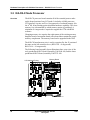
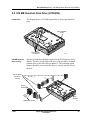
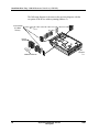
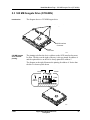
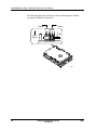
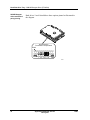
1
X
Application Module Service
AX13-510
Application ModuleX
X
Application Module Service
AX13-510
Release 110/200
CE Compliant
12/01
Copyright, Notices, and Trademarks
Copyright 1995-1999 by Honeywell Inc.
Revision 05 – December 13, 2001
While this information is presented in good faith and believed to be accurate, Honeywell
disclaims the implied warranties of merchantability and fitness for a particular purpose and makes
no express warranties except as may be stated in its written agreement with and for its customers.
In no event is Honeywell liable to anyone for any indirect, special or consequential damages. The
information and specifications in this document are subject to change without notice.
This publication supports TotalPlant Solution (TPS) system software release 500 and later, and
CE Compliant hardware.
Honeywell, TotalPlant, and TDC 3000 are U.S. registered trademarks of Honeywell Inc.
Other brand or product names are trademarks of their respective owners.
The following standard document conventions may be used in this document. Check Section 1
for the conventions that are unique to this document.
Item
Convention
Meaning
<KEYCAPS>
Pointed brackets around a term
A keyboard key
[TARGET]
Square brackets around a term
For touchscreen monitors,
an area that can be touched
to invoke a system action.
entry data
Courier bold text
Data that you enter into the
system.
Screen/program data
Courier text
Screen or program data
Honeywell Inc.
Industrial Automation and Control
Automation College
2820 West Kelton Lane
Phoenix, AZ 85023
1-800-852-3211
Contents
1.
INTRODUCTION............................................................................................................................. 7
1.1
About This Document ............................................................................................................... 7
1.2
References ................................................................................................................................. 8
X
2.
APPLICATION MODULE .............................................................................................................. 9
X
2.1
A M Functionality ...................................................................................................................... 9
2.2
Hardware Organization ........................................................................................................... 11
2.3
Board Slot Definition ............................................................................................................... 13
2.4
Power Supply ........................................................................................................................... 16
3.
HARDWARE DESCRIPTION OF LCN NODE PROCESSORS................................................... 17
3.1
K2LCN-X Node Processor ...................................................................................................... 17
3.2
K4LCN-X Node Processor ...................................................................................................... 22
3.3
HMPU Processor and Associated Boards ............................................................................ 29
3.4
CLCN A/B I/O Board (or LCN I/O Board) ............................................................................... 34
3.5
Node Processor Related Board Replacement ...................................................................... 36
4.
HARDWARE DESCRIPTION OF COPROCESSOR.................................................................... 37
4.1
WSI2 Board Description.......................................................................................................... 37
4.2
WSI2 I/O Board Description.................................................................................................... 50
4.3
Media Access Unit (MAU) Description .................................................................................. 50
4.4
WSI2 Board Replacement ....................................................................................................... 53
4.5
WSI2 I/O Board replacement .................................................................................................. 56
5.
HARD DISK DRIVE TRAY ........................................................................................................... 59
5.1
Drive Tray Description ............................................................................................................ 59
5.2
525 MB Quantum Disk Drive (LPS525S)................................................................................ 65
5.3
525 MB Seagate Drive (ST3600N)........................................................................................... 67
5.4
GB Digital Equipment Corp. Drive (DSP3107L) .................................................................... 72
5.5
GB Quantum Drive (LPS1080S).............................................................................................. 74
5.6
GB Quantum Drive (VP31110) ................................................................................................ 76
5.7
GB Seagate Drive (ST31200) .................................................................................................. 78
5.8
2 GB Quantum Drive (VP32210) ............................................................................................. 82
5.9
2 GB Seagate Drive (ST32430N)............................................................................................. 84
5.10
2 GB Hewlett Packard Drive (C3325A) ............................................................................... 86
5.11
4 GB Seagate Drive (ST34572N) ......................................................................................... 89
12/01
Application ModuleX Service
Honeywell
iii
Contents
5.12
HDDT I/O Board ....................................................................................................................91
5.13
Disk Drive/Drive Tray Replacement....................................................................................92
5.14
HDDT I/O Board Replacement.............................................................................................95
6.
COPROCESSOR CONSOLE .......................................................................................................97
6.1
Overview ...................................................................................................................................97
6.2
Coprocessor Terminal Description and Configuration........................................................99
6.3
Coprocessor Console Terminal Connection.......................................................................100
7.
TAC ACCESS TO COPROCESSOR..........................................................................................105
7.1
Overview .................................................................................................................................105
7.2
Communications Modem Description and Configuration .................................................107
7.3
Modem Connection................................................................................................................110
8.
HP 712/60 PA RISC DESKTOP WORKSTATION .....................................................................113
8.1
9.
DAT DRIVE .................................................................................................................................115
9.1
Introduction ............................................................................................................................115
9.2
DAT Drive Indicators .............................................................................................................116
9.3
Preventive Maintenance ........................................................................................................117
9.4
DAT Drive Physical Configuration and Cabling..................................................................118
9.5
DAT Replacement ..................................................................................................................123
10.
SECTION 10—CD-ROM DRIVE .................................................................................................125
10.1
Introduction.........................................................................................................................125
10.2
CD-ROM Physical Configuration and Cabling.................................................................126
10.3
CD-ROM Replacement .......................................................................................................130
11.
iv
X
HP 712/60 Workstation in A M Environment.......................................................................113
SPARE PARTS ...........................................................................................................................133
11.1
Overview..............................................................................................................................133
11.2
Basic 5-Slot Module Parts .................................................................................................134
11.3
Basic 10-Slot Module Parts ...............................................................................................136
11.4
LCN Node Processor Parts ...............................................................................................137
11.5
Coprocessor and Related Parts........................................................................................138
11.6
Hard Disk Drive Tray and Drive Parts ..............................................................................141
11.7
DAT Tape and Associated Parts .......................................................................................142
11.8
CD-ROM and Associated Parts .........................................................................................145
Application ModuleX Service
Honeywell
12/01
Tables
Tables
Table 2-1 Five-Slot Chassis Board Locations (32/64/128 MB Coprocessor Memory Sizes) ................. 13
Table 2-2 Five-Slot Chassis Board Locations (with 256 MB Coprocessor Memory).............................. 14
Table 2-3 Ten-Slot Chassis Board Locations ......................................................................................... 15
Table 2-4 Ten-Slot Chassis Board Locations (with 256 MB Coprocessor Memory) .............................. 15
Table 3-1 K2LCN Board Indicators ......................................................................................................... 19
Table 3-2 K4LCN Board Indicators ......................................................................................................... 25
Table 3-3 HMPU Error Indicators............................................................................................................ 30
Table 3-4 LLCN Indicators ...................................................................................................................... 32
Table 3-5 QMEM Memory Capacities..................................................................................................... 32
Table 3-6 QMEM Indicator ...................................................................................................................... 33
Table 3-7 Board Replacement Procedure .............................................................................................. 36
Table 4-1 Procedure to Obtain a Replacement Kinet License Key. ....................................................... 49
Table 4-2 LTX-2 Indicators and Switches ............................................................................................... 51
Table 4-3 WSI2 Board Replacement Procedure .................................................................................... 54
Table 4-4 WSI2 I/O Board Replacement Procedure............................................................................... 57
Table 5-1 Disk Drives Currently Available .............................................................................................. 62
Table 5-2 Drive Tray/Disk Drive Replacement Procedure...................................................................... 93
Table 5-3 HDDT I/O Board Replacement Procedure ............................................................................. 96
Table 6-1 Terminal Connection Procedure ........................................................................................... 103
Table 6-2 Cable/Connector Definition for Connecting Console Terminals. .......................................... 104
Table 7-1 U.S. Robotics 9600 Configuration Switch Positions ............................................................. 107
Table 7-2 U.S. Robotics 9600 Configuration Register Data ................................................................. 109
Table 7-3 Modem Connection Procedure ............................................................................................. 112
Table 9-1 DAT Drive Indicator Definitions............................................................................................. 116
Table 9-2 DAT Drive Head Cleaning Procedure................................................................................... 117
Table 9-3 DAT Replacement Procedure............................................................................................... 124
Table 10-1 CD-ROM Replacement Procedure ..................................................................................... 131
Table 11-1 5-Slot Module Parts List for Normal Production Units ........................................................ 134
Table 11-2 Basic 10-Slot Module Parts List for Normal Production Units ............................................ 136
Table 11-3 LCN Node Processor Related boards Parts List ................................................................ 137
Table 11-4 WSI2 and WSI2 I/O Boards ................................................................................................ 138
Table 11-5 Coprocessor Memory Boards and Battery ......................................................................... 139
Table 11-6 PIN Connection Hardware .................................................................................................. 140
Table 11-7 Coprocessor Console Terminal/Modem Interface Cables.................................................. 140
Table 11-8 Drive Tray and Related Parts List....................................................................................... 141
Table 11-9 DAT Drive and Associated Spare Parts ............................................................................. 142
Table 11-10 DAT Drive and Associated Spare Parts ........................................................................... 143
Table 11-11 DAT Drive and Associated Spare Parts ........................................................................... 144
Table 11-12 CD-ROM and Associated Spare Parts ............................................................................. 145
Table 11-13 CD-ROM and Associated Spare Parts ............................................................................. 146
Table 11-14 CD-ROM and Associated Spare Parts ............................................................................. 146
12/01
Application ModuleX Service
Honeywell
v
Tables
vi
Application ModuleX Service
Honeywell
12/01
1. Introduction
1.1 About This Document
Basics
Purpose
This manual provides instructions for maintenance and repair of
X
the Application Module .
Intended All personnel that are expected to perform hardware installation,
Audience troubleshooting, and repair activities on the Application ModuleX.
For Product This publication supports TotalPlant Solution (TPS) system
Release software release 500 and later, and CE Compliant hardware.
Product description
The Application ModuleX is an LCN node that combines the Application Module
(AM) functionality with an HP-UX-based coprocessor.
CE Compliant hardware
Any equipment designated as "CE Compliant" complies with the European Union
EMC and Health and Safety Directives. All equipment shipping into European
Union countries after January 1, 1996 require this type of compliance—denoted by
the "CE Mark
12/01
Application ModuleX Service
Honeywell
7
Introduction – References
1.2 References
For more information
The following documentation is referenced from within this document:
Publication Title
Publication
Number
Binder Title
Binder
Number
X
AX11-300
Application Module
X
3094
X
AX13-300
Application Module
X
3094
Application Module User Guide
X
AX09-300
Application Module
X
3094
Five/Ten-Slot Service
LC13-500
LCN Service
Application Module System
Administration
Application Module
Troubleshooting
3060-2
X
Licensing Installation and
X
Administration A M
LA20-200
Application Module
Universal Station Service
US13-500
LCN Service-1
3060-1
Universal Station (Ergonomic)
Service
US13-520
LCN Service-1
3060-1
UX13-510
Universal Station
X
Universal Station Service
8
Application ModuleX Service
Honeywell
X
3094
3095
12/01
2. Application ModuleX
2.1 AXM Functionality
General
introduction
Supports existing
AM functionality
12/01
The Application ModuleX (AXM) provides the functionality of a
standard Application Module (AM) coupled with an HP-UX-based
coprocessor.
This hardware combination provides the capability for delivering
powerful higher level control schemes to the TDC 3000X. It also
provides the capability of adapting and utilizing third party control
solutions.
Two performance levels of the coprocessor are available. The basic
coprocessor operates at 64 MHz and a high performance coprocessor
will operate at 100 MHz.
The AXM continues to provide the full functionality of the existing
Application Modules (AM). This is accomplished by the LCN node
processor portion in the AXM
Application ModuleX Service
Honeywell
9
Application ModuleX – AXM Functionality
Functionality
Diagram
The following diagram illustrates that there are two distinct processors
in the AXM node. A standard LCN node processor is coupled to an HPUX-based coprocessor.
The total AXM software responsibility of both processors is identified by
the dotted lines.
Notice that both processors must work through their respective portions
of the communication software to successfully pass information between
them.
X applications will be executed in the coprocessor. Access to LCN point
data is done through the LCN node processor. The Control Language
(CL) running in the node processor has been modified to include
mechanisms for calling and starting solutions resident in the
coprocessor.
Plant Information
Network (PIN)
Coprocessor
(UNIX)
Software
HP-UX
X Application
LCN Server
Hard
Drive(s)
Communication
Interface
LCN
Node
Processor
AM
- AM (CL)
- Points
- Custom Data
Segments
Local Control
Network (LCN)
10
Application ModuleX Service
Honeywell
40000
12/01
Application ModuleX – Hardware Organization
2.2 Hardware Organization
AXM Hardware
block diagram
Two versions of AXM hardware will be available. One uses the K2LCN
(or K4LCN) board as the LCN node processor and the other uses the
HMPU/ LLCN/QMEM combination of boards as the LCN node
processor.
The diagrams on the following two pages show the major hardware
components that make up the AXM hardware. Pay particular attention to
the following:
•
Names and acronyms of the components
•
Interconnection between components
•
External connections to:
– Local Control Network (LCN)
– Plant Information Network (PIN)
– “Console terminal” (when required for initial configuration or
troubleshooting). A console terminal is a simple keyboard and
display device that has no processing capability. Several device
types can be used to satisfy this requirement. They are addressed
later in this manual.
– Modem for Technical Assistance Center (TAC) access (if
required for complex problem isolation activities).
– DAT drive (optional) to support hard disk backup, restore, and
software update activities. It is also used for recovery activities in
the event of some hard disk drive failures.
– CD-ROM (optional) provides access to the HP-UX online
software documentation.
12/01
Application ModuleX Service
Honeywell
11
Application ModuleX – Hardware Organization
K2LCN/K4LCN
hardware version
Local Control Network
(LCN)
A
B
CLCN A/B
I/O *
Plant Information Network
(PIN)
WSI2 I/O
HDDT I/O
Backplane
Connection
CLCN A/B
I/O *
HDDT
SCSI
Interface Cable
Plant Information Network
(PIN)
DAT
Drive
(Optional)
Connection for
Console Terminal
or TAC Access
Modem
WSI2 I/O
Backplane Connection
LLCN
HMPU
LCN
Interface
Node
Processor
QMEM
Additional
Memory
(For HMPU)
WSI2
Coprocessor
* Non-CE compliant nodes use an LCN I/O
12
Hard Disk
Drive Tray
40134
The following diagram illustrates the HMPU version of hardware.
Local Control Network
(LCN)
A
B
CD-ROM
(Optional)
Connection for
Console Terminal
or TAC Access
Modem
K4LCN
WSI2
(or K2LCN)
Coprocessor
Node
Processor
* Non-CE compliant nodes use an LCN I/O
HMPU hardware
version
DAT
Drive
(Optional)
Application ModuleX Service
Honeywell
CD-ROM
(Optional)
HDDT I/O
HDDT
SCSI
Interface Cable
Hard Disk
Drive Tray
40021
12/01
Application ModuleX – Board Slot Definition
2.3 Board Slot Definition
Overview of
chassis types
Five-Slot board
placement
The AXM will appear in two types of LCN node hardware chassis. They
are
Five-slot chassis (when using a K2LCN/K4LCN node processor)
Ten-slot chassis (when using an HMPU node processor)—This specific
Ten-slot chassis has a split backplane with 6 slots (bottom) dedicated to
one LCN node and 4 slots (top) for another LCN node. This Ten-slot
chassis has been used in other special LCN applications. A second node
in slots 7-10 is not allowed in the case of an AXM.
The following tables show the AXM board placement for the Five-slot
chassis using the K4LCN or K2LCN node processor.Two versions of
board placement are used depending on the size of the coprocessor
memory which is located on the WSI2 board. The 256 megabyte size
requires additional space above the WSI2 board.
Table 2-1 Five-Slot Chassis Board Locations (32/64/128 MB Coprocessor Memory Sizes)
Slot
Front
5
Optional Application Board
4
Hard Disk Drive Tray
(occupies two slots)
3
2
1
12/01
WSI2 *
K2LCN-8
or
K4LCN-8 ( or -16)
Rear
HDDT I/O
WSI2 I/O
CLCN A/B
or
LCN I/O **
Application ModuleX Service
Honeywell
13
Application ModuleX – Board Slot Definition
Table 2-2 Five-Slot Chassis Board Locations (with 256 MB Coprocessor Memory)
Slot
5
Front
Hard Disk Drive Tray
(occupies two slots)
4
3
HDDT I/O
(Space for extra WSI2 Memory)
WSI2 *
2
1
Rear
WSI2 I/O
K2LCN-8
or
K4LCN-8 ( or -16)
CLCN A/B
or
LCN I/O **
* Two versions of the WSI2 board are available to provide the 64 MHz and 100
MHz coprocessors.
** Non-CE Compliant versions use the LCN I/O.
Ten-slot board
placement
14
The following two tables show the AXM board placement for the 10-slot
chassis using the HMPU node processor. Two versions of board
placement are used depending on the size of the coprocessor memory
which is located on the WSI2 board. The 256 megabyte size requires
additional space above the WSI2 board.
Slots 7 through 10 do not share a common backplane for interconnection
with slots 1 through 6.
The Hard Drive Disk tray does not depend on the backplane for signal
interconnection with other slots. It only uses the slots it occupies to
obtain power, which is common to all slots.
Application ModuleX Service
Honeywell
12/01
Application ModuleX – Board Slot Definition
Table 2-3 Ten-Slot Chassis Board Locations
Slot
Front
10
Unusable slot
9
Unusable slot
8
Hard Disk Drive Tray
7
(occupies two slots)
6
WSI2 *
5
Optional Application board
4
Optional memory board
3
QMEM-4
2
LLCN
1
HMPU
Rear
HDDT I/O
WSI2 I/O
CLCN A/B
or
LCN I/O **
* Two versions of the WSI2 board are available to provide the 64 MHz and 100
MHz coprocessors.
** Non-CE Compliant versions use the LCN I/O.
Table 2-4 Ten-Slot Chassis Board Locations (with 256 MB Coprocessor Memory)
Slot
Front
10
Unusable slot
9
Unusable slot
8
Hard Disk Drive Tray
7
(occupies two slots)
6
(Space for extra WSI2 memory)
5
WSI2 *
4
Optional Application board
3
QMEM-4
2
LLCN
1
HMPU
Rear
HDDT I/O
WSI2 I/O
CLCN A/B
or
LCN I/O **
* Two versions of the WSI2 board are available to provide the 64 MHz and 100
MHz coprocessors.
** Non-CE Compliant versions use the LCN I/O.
12/01
Application ModuleX Service
Honeywell
15
Application ModuleX – Power Supply
2.4 Power Supply
The AXM node contains a power supply (55 amp) that is used in many
other LCN node types.
It is capable of producing output voltage margins of +5% and -5% that,
in some cases, are used in factory test and troubleshooting activities. This
margining is controlled by the jumper on the face of the power supply.
See the following diagram.
Similar power supplies are used in both the K2LCN/K4LCN (Five-slot)
and HMPU (Ten-slot) versions of AXM.
Introduction
Node power
margin
restrictions
WARNING
The low power margin (-5%) must never be used in the
X
A M. The coprocessor and hard disk drive design allows
for only a -2.5% margin. Using -5% margins will produce
unpredictable results.
The high (+5%) power margin can be used by factory test
and during troubleshooting activities. Honeywell does not
recommend using any power margins while a node is on
process.
Node power
supply diagram
The following diagram shows the power supply in a Five-slot chassis
(K2LCN/K4LCN version). A similar power supply is used in the Tenslot chassis (HMPU version).
5
4
3
2
1
5-Slot
Chassis
Norm
Lo
Power
Supply
16
Error
Power
OK
Reset
Button
Hi
Margins Test
Jumper
Application ModuleX Service
Honeywell
Power On/Off
Switch
Fan
Module
40047
12/01
3. Hardware Description of LCN Node Processors
3.1 K2LCN-X Node Processor
Overview
K2LCN indicators
The K2LCN processor board contains all of the essential parts to make
up the kernel portion of any LCN node. It includes a 68020 processor,
LCN interface circuits, and 6 or 8 megawords of on-board memory (for
AXM). It does not have floating point calculation hardware capability.
The exact memory size is determined by which option is purchased. A
minimum of 6 megawords is required to support R500 software.
Changing memory size requires the replacement of the current K2LCN
board with a board containing the proper memory complement. This
board cannot be upgraded in the field.
The K2LCN board memory size is easily recognized by the -X portion of
the name on the left extraction lever; i.e., K2LCN-6 = 6 megawords or
K2LCN-8 = 8 megawords.
The K2LCN board indicators are visible from thefree edge of the board
while the board is installed in a module chassis. The indicators provide a
visual indication regarding the present condition of the board.
Two illustrations of the indicators follow. The first illustration shows the
indicator layout on an early production K2LCN board, assembly
51401551-x00. The second illustration shows the indicators on the latest
production K2LCN board, assembly 51402615-x00.
The indicators provide identical information on both boards.
The indicators on the early production K2LCN board, assembly
51401551-x00, are shown in the following illustration.
Data
DTAK BGAK
RST/PWR Self-Test Compare Time Time
Fail
Error
Error
Out
Out
Self-Test
Pass
(Green)
Data
Parity
Error
Bus
Error
EDAC
Multi-Bit
Error
LCN
Transaction
Error
Node
Address/Error
Display
TX
(Yellow)
Red LEDs
12/01
EDAC
Single-Bit
Error
Application ModuleX Service
Honeywell
40022
17
Hardware Description of LCN Node Processors – K2LCN-X Node Processor
The indicators on the latest production K2LCN borad, assembly 51402615-x00, are
shown in the following illustration.
Self-Test
Error
RST/PWR
Fail
DTAK
Time
Out
Data
Compare
Error
Data
Parity
Error
BGAK
Time
Out
TX
(Yellow)
Red LEDs
18
EDAC
Multi-Bit
Error
LCN
Transaction
Error
Node
Address/Error
Display
Self-Test
Pass
(Green)
Bus
Error
EDAC
Single-Bit
Error
Application ModuleX Service
Honeywell
34054
12/01
Hardware Description of LCN Node Processors – K2LCN-X Node Processor
The following table provides descriptions of the indicators on the
K2LCN board. Reference the preceding diagrams.
Indicator
description
Table 3-1 K2LCN Board Indicators
LED
Description
Suspected cause if abnormal
Self-Test Pass
On after board passes self-test.
Normally on.
K2LCN
TX
On when transmitting on the
LCN. Normally on or flashing
rapidly.
K2LCN
RST/PWR fail
On when a reset operation
caused by the reset button or
power on is in progress.
Normally off.
K2LCN
Self-Test Error
On to indicate a board self-test
error. Normally off.
K2LCN
Data Compare Error
On to indicate an on-board data
compare error. Normally off.
K2LCN
DTAK Time Out
On to indicate a Data Transfer
Acknowledge failure. Normally
off.
K2LCN
BGAK Time Out
On to indicate a Bus Grant
Acknowledge failure. Normally
off.
K2LCN or other board(s) in
chassis
Data Parity Error
On to indicate an on-board data
parity error. Normally off.
K2LCN
Bus Error
On to indicate a detected
backplane bus parity error.
Normally off.
K2LCN, other board(s) in
chassis, or backplane
EDAC Single-Bit Error
On to indicate a single-bit
(correctable) RAM error.
Normally off.
K2LCN
EDAC Multiple-Bit Error
On to indicate a multiple-bit
(uncorrectable) RAM error.
Normally off.
K2LCN
LCN Transaction Error
On to indicate communication
K2LCN or CLCN A/B (LCN I/O)
problems with the LCN. Normally or
off.
LCN network
12/01
Application ModuleX Service
Honeywell
19
Hardware Description of LCN Node Processors – K2LCN-X Node Processor
K2LCN Pinning
The K2LCN board has an LCN node number pinning feature on the
board itself. This feature is duplicated on the CLCN A/B I/O or LCN I/O
board that is installed directly behind the K2LCN board in the AXM
Five-Slot Module chassis.
ATTENTION
The address pinning jumpers must all be removed from the
K2LCN board when it is used in conjunction with an CLCN
A/B I/O (or LCN I/O) board. The node number pinning must be
done on the CLCN A/B I/O (or LCN I/O) board in this case.
The K2LCN board pinning requirement for the AXM is shownin the
following two illustrations.
The first illustration shows the location of the address pinning lbock on
the early production K2LCN board, assembly 51401551-x00. The second
illustration shows the location of the address pinning block on the latest
production K2LCN board, assembly 51402615-x00.
20
Application ModuleX Service
Honeywell
12/01
Hardware Description of LCN Node Processors – K2LCN-X Node Processor
NOTE: This text is not on the board.
Binary
Weight
Parity
5 6 P
TS2
64
3 4
32
9C
16
0 1 2
8
9D
4
2
1
9F
9H
Jumper Removed = "1"
K2LCN
40002
6 P
Binary
Weight
Parity
NOTE: This text is not on the board.
TS1
5
64
5C
3 4
32
7A
16
1 2
8
4
0
2
1
Jumper Removed = "1"
K2LCN
16572
12/01
Application ModuleX Service
Honeywell
21
Hardware Description of LCN Node Processors – K4LCN-X Node Processor
3.2 K4LCN-X Node Processor
Overview
The K4LCN processor board contains all of the essential parts to make
up the kernel portion of any LCN node. It includes a 68040 processor,
LCN interface circuits, and 8 or 16 megawords of on-board memory (for
the AXM). It has floating point calculation hardware capability. The exact
memory size is determined by which memory option is purchased. A
minimum of 6 megawords is required to support the AXM with R500
software.
Changing memory size requires the replacement of the existing memory
daughter board or mezzanine board with a board that contains the proper
memory complement. The memory board can be upgraded in the field.
The K4LCN board memory size is easily recognized by the -X portion of
the name on the left extraction lever. (K4LCN-8 = 8 megawords,
K4LCN-16 = 16 megawords).
The following board assembly layout illstrations show a top view of the
early production K4LCN board, assembly 51401946-100, and the latest
production K4LCN board, assembly 51402755-100.
LCN Address Pinning
Memory Board
ASSY.
51401946-100
52521
22
Application ModuleX Service
Honeywell
12/01
Hardware Description of LCN Node Processors – K4LCN-X Node Processor
Memory Board
K4LCN
LCN Address Pinning
ASSY. NO.
51402755-100
16571
12/01
Application ModuleX Service
Honeywell
23
Hardware Description of LCN Node Processors – K4LCN-X Node Processor
K4LCN indicators
The K4LCN board indicators are visible at the free edge of the board
while it is installed in the module chassis. They provide visual indication
of the existing conditions of the board. See the illustration below.
Data
DTAK BGAK
RST/PWR Self-Test Compare Time Time
Fail
Error
Error
Out
Out
Self-Test
Pass
(Green)
Data
Parity
Error
Bus
Error
EDAC
Multi-Bit
Error
EDAC
Single-Bit
Error
LCN
Transaction
Error
Node
Address/Error
Display
TX
(Yellow)
Red LEDs
Indicator
description
24
40022
The following table provides a description of the indicators on the
K4LCN board. Reference the preceding diagram.
Application ModuleX Service
Honeywell
12/01
Hardware Description of LCN Node Processors – K4LCN-X Node Processor
Table 3-2 K4LCN Board Indicators
LED
Description
Suspected cause if abnormal
Self-Test Pass
On after board passes self-test.
Normally on.
K4LCN
TX
On when transmitting on the
LCN. Normally on or flashing
rapidly.
K4LCN
RST/PWR fail
On when a reset operation
caused by the reset button or
power on is in progress.
Normally off.
K4LCN
Self-Test Error
On to indicate a board self-test
error. Normally off.
K4LCN
Data Compare Error
On to indicate an on-board data
compare error. Normally off.
K4LCN
DTAK Time Out
On to indicate a Data Transfer
Acknowledge failure. Normally
off.
K4LCN
BGAK Time Out
On to indicate a Bus Grant
Acknowledge failure. Normally
off.
K4LCN or other board(s) in
chassis
Data Parity Error
On to indicate an on-board data
parity error. Normally off.
K4LCN
Bus Error
On to indicate a detected
backplane bus parity error.
Normally off.
K4LCN, other board(s) in
chassis, or backplane
EDAC Single-Bit Error
On to indicate a single-bit
(correctable) RAM error.
Normally off.
K4LCN
EDAC Multiple-Bit Error
On to indicate a multiple-bit
(uncorrectable) RAM error.
Normally off.
K4LCN
LCN Transaction Error
On to indicate communication
K4LCN or CLCN A/B I/O
problems with the LCN. Normally (LCN I/O) or LCN network
off.
See Five/Ten-Slot Module
This 3-digit display normally
Service manual for multiple
displays the pinned LCN node
possible causes. Reference
address. It will display error
>>Alpha Numeric Displays in
codes for further problem
Appendix A.
definition in error situations.
Node Address/Error display
12/01
Application ModuleX Service
Honeywell
25
Hardware Description of LCN Node Processors – K4LCN-X Node Processor
K4LCN Pinning
The K4LCN board has an LCN node number pinning feature on the
board itself. This feature is duplicated on the CLCN A/B I/O or LCN I/O
board that is installed directly behind the K4LCN board in the AXM
Five-Slot Module chassis.
ATTENTION
The address pinning jumpers must all be removed from the
K4LCN board when it is used in conjunction with a CLCN
A/B I/O (or LCN I/O) board. The node number pinning must be
done on the CLCN A/B I/O (or LCN I/O) board in this case.
The following illustration shows the LCN address pinning for a K4LCN
board when used in the AXM’s Five-Slot Module chassis.The illustration
shows the location of the pinning block, TS2, on the early production
K4LCN board, assembly 51401946-100.
NOT ON BOARD
P
LCN Address
Pinning
1 2 3 4 5 6
LCN ADDRESS
PARITY
64
32
16
BINARY
WEIGHT
8
4
0
2
1
1
0
52585-A
The pinning requirements are the same for the latest production K4LCN
board, assembly 51402755-100. Refer to the previous illustration of the
board’s assembly layout for the approximate location of the pinning block,
TS1.
26
Application ModuleX Service
Honeywell
12/01
Hardware Description of LCN Node Processors – K4LCN-X Node Processor
K4LCN Memory
Memory for the K4LCN board is provided by a vertically pluggable
daughter board on the early production K4LCN board, assembly
51401946-100, and a horizontally pluggable DIMM (Dual Iline Memory
Module) style mezzanine board on the latest production K4LCN board,
assembly 51402755-100.
The memory daughter board is also sometimes referred to as a mezzanine
board.
The memory boards are available in three memory sizes, 4, 8, and 16
megawords.
When a replacement K4LCN board is ordered from Honeywell logistics, it
is provided without a memory board. The appropriate size memory board
should also be ordered separately to prevent the possibility of moving a
defective memory board from the failed K4LCN board to the replacement
board.
The size of the memory on the K4LCN board is upgraded in the field by
replacing the memory board.
Earlier memory boards, such as EMEM, PMEM, or QMEM, that were
used with earlier node processor boards cannot be used with the K4LCN
board.
The following illustrations show the installation of the memory boards on
the early and latest production K4LCN boards.
LCN Address Pinning
Memory Board Location
Screws
52584
12/01
Application ModuleX Service
Honeywell
27
Hardware Description of LCN Node Processors – K4LCN-X Node Processor
Memory Board
K4LCN
LCN Address Pinning
ASSY. NO.
51402755-100
16570
28
Application ModuleX Service
Honeywell
12/01
Hardware Description of LCN Node Processors – HMPU Processor and Associated Boards
3.3 HMPU Processor and Associated Boards
Overview
The HMPU node processor has a 68020 microprocessor and includes
floating point calculation hardware capability. It also has 2 megawords of
on-board memory.
Additional memory for the HMPU processor in the AXM node is provided
by a QMEM board. A minimum of 6 megawords is required to support
R500 software.
The HMPU board does not have LCN interface circuits and consequently
must always have an LLCN board as its partner to form the kernel for the
AXM LCN node.
HMPU Indicators
The HMPU board indicators are visible from the free edge of the board
while it is installed in a chassis. They provide visual indications
regarding the existing conditions on the board.
An indicator diagram follows:
The HMPU indicators are illustrated in the following diagram:
Data
RST/PWR Self-Test Compare
Fail
Error
Error
DTAK BGAK
Time Time
Out
Out
Data
Parity
Error
Bus
Error
EDAC
Multi-Bit
Error
Pass MOD
Test
(Green)
Node
Address/Error
Display
Red LEDs
12/01
EDAC
Access
Single-Bit
Violation
Error
(HMPU Only)
Application ModuleX Service
Honeywell
40023
29
Hardware Description of LCN Node Processors – HMPU Processor and Associated Boards
The following table gives a description of the indicators on the HMPU
board. Reference the preceding diagram.
Indicator
description
Table 3-3 HMPU Error Indicators
LED
Description
Suspected cause if abnormal
Pass Module Test
On after board passes self-test.
Normally on.
HMPU
RST/PWR Fail
On when a reset operation
caused by the reset button or
power on is in progress.
Normally off.
HMPU
Self-Test Error
On to indicate a board self-test
error. Normally off.
HMPU
Data Compare Error
On to indicate an on-board data
compare error. Normally off.
HMPU
DTAK Time Out
On to indicate a Data Transfer
Acknowledge failure. Normally
off.
HMPU
BGAK Time Out
On to indicate a Bus Grant
Acknowledge failure. Normally
off.
HMPU or other board(s) in
chassis
Data Parity Error
On to indicate an on-board data
parity error. Normally off.
HMPU
Bus Error
On to indicate a detected
backplane bus parity error.
Normally off.
HMPU, other board(s) in chassis,
or backplane
EDAC Single-Bit Error
On to indicate a single-bit
(correctable) RAM error.
Normally off.
HMPU
EDAC Multiple-Bit Error
On to indicate a multiple-bit
(uncorrectable) RAM error.
Normally off.
HMPU
Access Violation
On to indicate a memory access
violation. Normally off.
(Frequently on with Bus error or
EDAC Multiple bit error
indicators.)
HMPU or another board in the
chassis.
Node Address/Error display
This 3-digit display normally
displays the pinned LCN node
address. It will display error
codes for further problem
definition in error situations.
See Five/Ten-Slot Service
manual for multiple possible
causes. Reference >>Alpha
Numeric Displays in appendix A.
30
Application ModuleX Service
Honeywell
12/01
Hardware Description of LCN Node Processors – HMPU Processor and Associated Boards
LLCN board
functionality
LLCN board
indicators
The LLCN board provides the LCN interface functionality used by the
HMPU node processor. The actual connection to the LCN cables is
through the CLCN A/B I/O (or LCN I/O) board which is inserted in the
I/O card chassis immediately behind the LLCN board (same board slot).
The LCN node address is pinned on the CLCN A/B I/O (or LCN I/O)
board and is covered later in this section.
The LLCN board indicators are visible from the free edge of the board
when it is installed in a chassis. They provide visual indications
regarding the existing conditions on the board. An illustration is provided
below.
The LLCN indicators are illustrated below.
LLCN
Self
Test/Error
12/01
Pass
Mod Test
Bus
Trans Error
TX
Application ModuleX Service
Honeywell
40024
31
Hardware Description of LCN Node Processors – HMPU Processor and Associated Boards
LLCN indicator
description
The following table gives a description of the indicators on the LLCN
board. Reference the preceding diagram.
Table 3-4 LLCN Indicators
LED
Description
Suspected cause if abnormal
Self-Test/Error
On to indicate a board self-test
error. Normally off.
LLCN
Pass module test
On after board passes self-test.
Normally on.
LLCN
Bus Trans Error
On to indicate a detected
backplane bus parity error.
Normally off.
LLCN, other board(s) in chassis,
or backplane
Tx
Transmission on LCN from this
board is taking place. Normally
on or blinking rapidly (on a
loaded node).
LLCN, HMPU, or LCN cable
problems.
QMEM-X board
This board is used to provide additional memory for the HMPU node
processor. The 4 megaword version is required in the AXM with R500. A
total of 6 megawords of node processor memory is required to support
R500 (HMPU=2 + QMEM-4 = 4).
The memory size of any QMEM can quickly be determined by looking at
the last digit of the name on the left board extraction lever.
Example:
Table 3-5 QMEM Memory Capacities
Board name
Memory capacity
QMEM-2
2 Megawords
QMEM-3
3 Megawords
QMEM-4
4 Megawords
32
Application ModuleX Service
Honeywell
12/01
Hardware Description of LCN Node Processors – HMPU Processor and Associated Boards
QMEM indicators
The QMEM board indicators are visible from the free edge of the board
while it is installed in a chassis. They provide visual indications
regarding the existing conditions on the board. An illustration is provided
below.
QMEM-X
Pass
Mod Test
QMEM indicator
description
Data
Par
Sing
Bit
MULT
40025
The following table gives a description of the QMEM indicators.
Reference the preceding diagram.
Table 3-6 QMEM Indicator
LED
Description
Suspected cause if abnormal
Pass Mod test
On after board passes self-test.
Normally on.
Data Par
Parity error detected on incoming Another board in node,
data from the backplane module backplane, or QMEM
bus. Normally off.
Sing Bit
On to indicate a single bit
(recoverable) error exists.
Normally off.
QMEM
Mult
On to indicate a multiple bit
(unrecoverable) error exists.
Normally off.
QMEM
12/01
Application ModuleX Service
Honeywell
QMEM
33
Hardware Description of LCN Node Processors – CLCN A/B I/O Board (or LCN I/O Board)
3.4 CLCN A/B I/O Board (or LCN I/O Board)
Overview
This board provides the physical interface to the LCN cables. It is used
with both versions of node processors (K2LCN/K4LCN and HMPU).
The AXM LCN address pinning feature for defining the LCN physical
node number is located on this board. These address jumpers must be
properly configured at the time of hardware installation.
See the Five/Ten-Slot Service manual for additional pinning
details.Reference: >> LCN I/O Pinning (Section 2.8)
LCN address
pinning
CAUTION
Conflict in pinning possible—The K2LCN (or K4LCN)
processor board has a duplicate LCN node pinning feature.
The address jumpers on the K2LCN/K4LCN must all be
removed when it is used in conjunction with an CLCN A/B I/O
(or LCN I/O) board.
The LCN node address pinning on a LCN I/O board is illustrated in the
diagram below. The pinning is identical on the CLCN A/B board.
Not on Board
Jumper Out = 1
Jumper In = 0
CLCN A/B I/O
Board
P
Sample is 43
2 3 4 5 6
LCN Address
PARITY
64
32
16
8
4
0
2
1
1
34
Note that addresses 0-127 could be set, but
software will allow only node addresses 1-64.
1
Binary
Weight
The overall number of jumpers out, including
the parity jumper, must be an odd number.
0
The 1 and 0 refer to DIP switch positions when
a switch assembly is installed in place of the
40027
jumper block.
Application ModuleX Service
Honeywell
12/01
Hardware Description of LCN Node Processors – CLCN A/B I/O Board (or LCN I/O Board)
LCN cable
connections
The AXM node processor is connected to the LCN cable network. These
LCN cables (A and B) are connected to the CLCN A/B I/O (or LCN I/O)
board as shown in the following diagram. This cabling scheme is the same
for each LCN node that uses the CLCN A/B I/O (or LCN I/O) board.
K2LCN, K4LCN, or LLCN Board
MODULE BUS
CLCN A/B I/O BOARD
LCN Node Address
Jumpers
LCN B Coax
LCN A Coax
40130
12/01
Application ModuleX Service
Honeywell
35
Hardware Description of LCN Node Processors – Node Processor Related Board Replacement
3.5 Node Processor Related Board Replacement
Overview
Node power must be turned off for the purpose of changing circuit
boards in the AXM node.
WARNING
Damage can result—Circuit board damage can result if you
do not practice proper ESD procedures or attempt to remove/
insert a circuit board with node power applied.
CAUTION
Mandatory steps—It is mandatory that appropriate software
X
shutdown procedures are followed for the A M coprocessor
prior to removing power from the node.
Failure to do so can cause damage to the HP-UX file structure
on the coprocessor hard disk.
ATTENTION
It is also highly recommended that you perform a node
processor software shutdown when preparing to power off the
X
A M node. This provides for an orderly departure from the
LCN network.
Locating
shutdown
procedure
Software shutdown procedures for the AXM coprocessor are documented
in Section 3 of the Application ModuleX System Administration manual.
Reference >> Application ModuleX System Administration manual
(Section 3.5).
Board Removal/ Replacement Procedure
Table 3-7 Board Replacement Procedure
Step
1
Turn off power using the switch on the node power supply.
2
Remove the board .
3
Verify that the replacement board pinning matches the existing board.
4
Insert the replacement board .
5
The node is now ready for power on and loading.
X
Perform the node loading procedures. Reference: >> A M System
Administration manual (Section 3).
6
36
Action
Application ModuleX Service
Honeywell
12/01
4. Hardware Description of Coprocessor
4.1 WSI2 Board Description
Overview
WSI2 board
illustration
The basic WSI2 board contains the coprocessor interface circuits
required to adapt the coprocessor into the AXM node hardware.
Reference the diagram below.
A coprocessor daughter board connects to the WSI2 mother board
through a specially provided connector on the WSI2 board. Several small
cables are also used to complete the total coprocessor to WSI2 board
connections.
The WSI2 board is normally referred to as a board assembly which
includes the coprocessor daughter board (with its associated memory)
and all on board cables.
Neither coprocessor (daughter board) nor the WSI2 (mother board) is
separately field replaceable. The complete WSI2 assembly will be
available as a single spare part.
The coprocessor memory (mounted on the coprocessor daughter board)
is ordered separately. The Spare Parts section of this manual supports
this ordering concept. Reference: Coprocessor Memory and Battery.
The diagram below illustrates how the WSI2 board assembly is
organized.
WSI2
Circuit Board
WSI2
Board
Assembly
Coprocessor
(Daughter Board)
LAN Cable
12/01
Serial Port 1
Cable
51147
Application ModuleX Service
Honeywell
37
Hardware Description of Coprocessor – WSI2 Board Description
WSI2 Board
indicators (LEDs)
and switch
The diagram below shows two indicators and a switch at the left. These
are the WSI2 board indicators. These indicators are directly visible with
the chassis front cover in place. The indicators are described as follows:
•
Transaction error (red LED)
Indicates that a data parity error or bus error was encountered during
normal operation on the backplane module bus.
•
WSCPU running (yellow LED)
When on indicates that the coprocessor software (HP-UX) is up and
running.
•
Shutdown Switch
The switch can be used to force a coprocessor (HP-UX) shutdown. It is
recommended that the keyboard method (as documented in the AXM
System Administration manual) be used whenever possible. Reference:
>>AXM System Administration manual (Section 3.5).
The positions of this switch are defined as follows:
To the left = Shutdown
To the right = Normal
•
38
The remainder of the diagram shows the connectors and indicators
on the coprocessor daughter board free edge. They are defined in a
later diagram.
Application ModuleX Service
Honeywell
12/01
Hardware Description of Coprocessor – WSI2 Board Description
WSI2 board
indicators
The diagram below describes the indicators on the WSI2 mother board.
The coprocessor daughter board portion is covered later in this section.
WSI2 Board
Indicators
Model 743
PS/2
1
A
B
R
S
2
3
2
PS/2
0
V
A
A
U
I
/
V
I
D
S
C
S
I
Boot...
Model 743
H Run...
P
P
a
r
a
l
l
e
l
Abt.
Sys.
Fail
Rst.
WSI2
Speaker
hp
Coprocessor Free Edge
Shutdown Switch (Left = Shutdown, Right = Normal)
WSCPU (Coprocessor) Running (Yellow)
Transaction Error (Red)
WSI2 board
pinning
51148
The WSI2 board has only one pinned option. The pinning defines if an
HMPU board or a K2LCN/K4LCN board is used as the node processor.
The interface to the HMPU node processor is somewhat different from
the K2LCN/K4LCN node processors.
WSI2
Circuit
Board
WSI2 Board
Assembly
Board Revision
Pinning
(Do Not Touch)
Coprocessor
(Daughter
Board)
12/01
16/32 Bit DMA
Operations
(Single Jumper)
Remove this
jumper for all
applications of
this board
(16 Bit).
40065
Application ModuleX Service
Honeywell
39
Hardware Description of Coprocessor – WSI2 Board Description
Calender clock
battery
Coprocessor
battery location
The coprocessor contains a time of day clock circuit which has a battery
backup. The clock circuits are maintained by this battery whenever node
power is removed.
This battery has a very long life (years), but it will eventually have to be
replaced.
Note the location of this battery on the coprocessor daughter board
shown in the diagram below. It is a separately listed item in the parts
list.
The following diagram illustrates the location of the coprocessor
battery. It may not be as clearly visible as shown here because an
additional memory board may be installed on your coprocessor. The
battery will be covered by the additional memory board, if it exists, it
must be removed to change the battery.
WSI2
Board
Assembly
Coprocessor
Battery
51162
40
Application ModuleX Service
Honeywell
12/01
Hardware Description of Coprocessor – WSI2 Board Description
Coprocessor
memory
The coprocessor, which plugs into the WSI2 board, itself can have one or
more daughter boards. These are the coprocessor memory boards. The
diagram below illustrates the position of these boards. The coprocessor
memory can be upgraded in the field by changing these boards.
The coprocessor memory daughter boards are mounted with two Phillips
screws threaded into standoffs on the coprocessor board. These screws
and associated washers must be removed to change the memory boards.
Exercise care when pushing on the replacement memory board to ensure
proper mating of the pins and sockets in the connectors.
Coprocessor
Memory
Boards
51149
12/01
Application ModuleX Service
Honeywell
41
Hardware Description of Coprocessor – WSI2 Board Description
Coprocessor
memory option
(32 megabytes)
The following two illustrations show the two methods of providing the
minimum 32 megabyte memory option in position on the coprocessor
board. Memory board availability at the time of manufacture will
determine which method is used.The first method consists of two 16
megabyte boards.
16 Megabytes
(Each Board)
51163
Second method
The illustration below shows the second method of providing the 32
megabyte memory option. It consists of only one 32 megabyte memory
board.
No Board
Installed
32 Megabytes
(Single Board)
52500
42
Application ModuleX Service
Honeywell
12/01
Hardware Description of Coprocessor – WSI2 Board Description
Coprocessor
memory option
(64 megabytes)
The following two illustrations show the two methods of providing the
64 megabyte memory option in position on the coprocessor board.
Memory board availability at the time of manufacture will determine
which method is used.The first method consists of two 32 megabyte
boards.
32 Megabytes
(Each Board)
52517
Second method
The illustration below shows the second method of providing the 64
megabyte memory option. It consists of only one 64 megabyte memory
board.
No Board
Installed
64 Megabytes
(Single Board)
51164
12/01
Application ModuleX Service
Honeywell
43
Hardware Description of Coprocessor – WSI2 Board Description
Coprocessor
memory option
(128 megabyte)
The illustration below shows the 128 megabyte memory option in
position on the coprocessor board.
64 Megabytes
(Each Board)
51165
44
Application ModuleX Service
Honeywell
12/01
Hardware Description of Coprocessor – WSI2 Board Description
Coprocessor
memory option
(265 megabyte)
The illustration below shows the 256 megabyte memory option in
position on the coprocessor board. Notice that there are two 64 megabyte
memory daughter boards stacked in two locations. The 64 megaword
memory daughter boards (4 each) make up 256 megabytes of total
memory.
The stacking of these memory daughter boards requires additional
clearence on the top side of the WSI2 board. The 256 megabyte version
of board placement must be used (described in Section 2 of this
document). The card slot above the WSI2 must remain empty to provide
the required space.
64 megabytes
(each board)
Total of four
boards (two
each stacked at
both locations)
54415
12/01
Application ModuleX Service
Honeywell
45
Hardware Description of Coprocessor – WSI2 Board Description
•
Boot/Run—(Green indicator) Blinks during the boot process and
turns on (steady) when the boot is completed.
•
SCSI—It is the interface used for connecting the coprocessor SCSI
(disk drive) interface to the disk drive tray through a cable.
•
AUI/VID-A—Provides the interface to the Plant Information
Network (PIN). The PIN is Honeywell’s terminology for the Local
Area Network (LAN).
•
RS-232-A—Commonly referred to as Serial Port 1. It provides the
interface for the coprocessor console (terminal) or TAC access
modem.
The diagram illustrates the coprocessor free edge and identifies the
components that apply to the AXM application of this board.
Coprocessor
Free Edge
Model 743
PS/2
1
A
B
R
S
2
3
2
PS/2
0
V
A
Model 743
Not Used for AX M
A
U
I
/
V
I
D
Boot...
H Run...
P
Abt.
Sys.
Fail
Rst.
Speaker
WSI2
Sys Fail—(Red indicator) Comes on at power on and turns off after
internal test routines complete successfully.
Not Used for AX M
hp
WSI2 Board
Indicators
•
S
C
S
I
Coprocessor free
edge illustration
The illustration below shows several items. Some of these are not used
in the AXM application and are identified as such. The following
describes the ones that are used.
P
a
r
a
l
l
e
l
Coprocessor free
edge
Serial Port 1
(Connected to WSI2
with Onboard Cable)
System Fail Indicator (Red)
Boot/Run Indicator (Green)
PIN (LAN) Interface
(Connected to WSI2
with Onboard Cable)
SCSI Interface
(to Hard Disk Drive Tray)
46
Application ModuleX Service
Honeywell
51166
12/01
Hardware Description of Coprocessor – WSI2 Board Description
Coprocessor PIN
connection details
The coprocessor is connected to the PIN network as shown in the
diagram.
The PIN connection is made at the coprocessor free edge. The PIN
connection is routed from this point:
•
Through a cable to the WSI2 mother board,
•
Through the mother board, chassis backplane, and on to the WSI2
I/O board,
•
To a cable connector on the WSI2 I/O board,
•
Through a cable to the Media Access Unit (MAU),
•
And the MAU connects to the PIN network.
(Transceiver)
AUI
J6
WSI2 I/O
Media Access
Unit
P
I
N
Backplane Connection
WSI2
WSI2 Circuit Board
Coprocessor
Pin Interface Connection
12/01
Application ModuleX Service
Honeywell
40028
47
Hardware Description of Coprocessor – WSI2 Board Description
Coprocessor SCSI
interface details
The coprocessor SCSI (hard disk drive) interface connection is made at
the coprocessor board free edge. From there it is routed:
•
Through a cable to the Hard Disk Drive tray (HDDT) internal circuit
board,
•
Through the internal HDDT circuit board to disk drive interface
cables and also through the backplane to the HDDT I/O board,
•
Through the HDDT I/O board to a cable connector.
The SCSI interface connector on the HDDT I/O board has a terminator
assembly installed if no optional DAT drive or optional CD-ROM is
connected. If one or both of the optional devices is connected, the device
at the end of the cable must be pinned to provide the bus termination.
SCSI Terminator or
Optional SCSI Device
(DAT/CD-ROM)
Connection
Backplane
Connection
WSI2 I/O
WSI2
HDDT
I/O
HDDT
Hard Disk Drive
Tray (Located
above WSI2
Board)
HDDT Circuit
Board
Coprocessor
First Hard
Disk Drive
SCSI Interface
Cable
Second Hard
Disk Drive
(Optional)
40029
Coprocessor
hardware
identification
number
48
Each coprocessor has a unique software visible hardware identification
number manufactured into the board. This hardware identification number is
tied directly to the user of the optional Honeywell Kinet software license.
Only users requiring DECnet communications support will have Kinet
software installed on the coprocessor system.
Application ModuleX Service
Honeywell
12/01
Hardware Description of Coprocessor – WSI2 Board Description
License key
Honeywell provides the appropriate Kinet license key (correlated to the
coprocessor hardware identification number) to the customer with the
Kinet software at the time of shipment. The customer must enter this
provided license key into the Kinet software configuration data.
Replacement of a WSI2 board assembly due to failure (or any other
reason) also changes the hardware identification number. This makes the
existing Kinet license key (originally provided) unusable and a new
Kinet license key must be obtained when the WSI2 board is changed.
The replacement Kinet license key is obtained in the following manner.
Table 4-1 Procedure to Obtain a Replacement Kinet License Key.
Step
Action
1
Install the new WSI2 board assembly as outlined in the replacement
procedure provided later in this section.
2
Power on the node and allow the coprocessor to complete its software
boot.
3
Sign on as a user.
This can be accomplished from any HP-UX compatible
X
device on the PIN (Workstation or U S) or the coprocessor
console (terminal).
4
Enter the command “/etc/lanscan”.
The last 12 characters after “0x” under Station Address is the new
coprocessor hardware identification number.
5
Having obtained the new hardware identification number, call the
Honeywell Technical Assistance Center (TAC) using telephone number
800-822- 7673.
Inform them that you have changed your Application
X
Module coprocessor hardware and give them the new
hardware identification number.
6
12/01
Honeywell will in turn, provide a new Kinet license key
which must be entered into the Kinet software configuration
X
data of your system. Reference >>A M System
Administration manual, Installing and Updating Software
(Section 5).
Application ModuleX Service
Honeywell
49
Hardware Description of Coprocessor – WSI2 I/O Board Description
The Honeywell license key information (correlated to the Internet
Protocol address) is obtained from Honeywell prior to system
installation. The customer creates a license file based on this information.
This license file is not affected by replacement of a WSI2 board
assembly. This activity is not required for AXM R110.
4.2 WSI2 I/O Board Description
The WSI2 I/O board provides the coprocessor connection to the PIN
(LAN) network. A connection for Serial Port 1 (coprocessor console
terminal or modem connection - J1) is also provided. The Video output
is not used in the AXM application.
BAR CODE
WSI2 I/O board
cable connections
ASSY NO.
51304924-200
REV C
WSI2 I/O
LAN
J6
Video
J3
Terminal J1
53352
4.3 Media Access Unit (MAU) Description
The Media Access Unit is the device that connects the AXM to the Plant
Information Network (PIN). It contains a transceiver device that adapts
the LAN interface of the coprocessor to the LAN (ethernet) cable.
There are many vendors that produce this type of device. The one shown
in the diagram is just one of the many available.
Power for the device is supplied from the AXM through the PIN interface
cable which is connected to the WSI2 I/O board J6.
Media Access Unit The following drawing illustrates one of the many types of MAU.
Purpose
diagram
50
Application ModuleX Service
Honeywell
12/01
Hardware Description of Coprocessor – Media Access Unit (MAU) Description
End View
Top View
LTX-2
Thin Coax Transceiver
IEEE 802.3 10Base2
To
Coprocessor
(WSI2 I/O)
1 0
RCV
RCV
HBE
To PIN
(Ethernet)
HBE
LANTRONIX
Heartbeat
Power
HBE
Switches
1 0
PWR
Indicators
Media Access unit
indicators
40044
Many of the MAU devices have indicators on them. The
following indicator and switch explanation is specifically for
the MAU shown in the previous diagram.
Table 4-2 LTX-2 Indicators and Switches
LED
Description
PWR (green)
“On” to indicate +12 volt power is applied from the WSI board through the
WS2 I/O board and interface cable. Normally “on.”
HBE (AMBER)
This feature (heartbeat) is not used with the Application ModuleX
coprocessor. Normally “off.”
Switch
12/01
Position Required
Comment
RCV
0
(Feature not used)
HBE
0
(Feature not used)
Application ModuleX Service
Honeywell
51
Hardware Description of Coprocessor – Media Access Unit (MAU) Description
Media Access Unit
connection
The following WSI2 I/O diagram identifies the MAU connection (J6).
Power is supplied to the MAU from the WSI2 I/O board through the
interface cable.
BAR CODE
ASSY NO.
51304924-200
REV C
WSI2 I/O
LAN
J6
To MAU
(PIN
Cable)
52
Video
J3 Terminal J1
Video
(Not used
for AX M)
Serial
Port 1
(Terminal
or Modem)
Application ModuleX Service
Honeywell
40046
12/01
Hardware Description of Coprocessor – WSI2 Board Replacement
4.4 WSI2 Board Replacement
Overview
Node power must be turned off for the purpose of changing circuit
boards in the AXM node.
WARNING
Damage Can Result—Circuit board damage can result if you
do not practice proper ESD procedures or attempt to
remove/insert a circuit board with node power applied.
CAUTION
Mandatory Steps—It is mandatory that appropriate software
X
shutdown procedures are followed for the A M coprocessor
X
prior to removing power from the A M node.
Failure to do so can cause damage to the HP-UX file
structure on the coprocessor hard disk.
ATTENTION
It is also highly recommended that you perform a
node processor software shutdown when
X
preparing to power off the A M node. This
provides for an orderly departure from the LCN
network.
Locating
shutdown
procedure
12/01
Software shutdown procedures for both the AXM coprocessor and node
processor are documented in the Application ModuleX System
Administration manual.
Application ModuleX Service
Honeywell
53
Hardware Description of Coprocessor – WSI2 Board Replacement
WSI2 Board
Replacement
Procedure
Table 4-3 WSI2 Board Replacement Procedure
Step
Action
1
Turn off the power using the switch on the node power supply.
2
Disconnect the SCSI interface cable from the coprocessor free edge. (It
runs between the WSI2 and the drive tray above it.) This may require
removal of an additional cable to gain access (PIN interface). Note the
position of both cables as you remove them.
3
Remove the WSI2 assembly by using the extraction/ insertion levers.
4
Verify that the replacement WSI2 assembly pinning matches the existing
board.
5
Ensure that the replacement WSI2 assembly has the proper size
coprocessor memory (complement of board/s) properly mounted on the
coprocessor board. These boards are plugged into sockets on the
coprocessor board and then fastened with two screws each.
Remember that the WSI2 and coprocessor memory are ordered
separately.
6
Insert the replacement WSI2 assembly using the extraction/insertion
levers.
7
Reconnect the cables removed in step 2. (SCSI and PIN interface
cables).
The node is ready for power on and loading. Turn on the power switch
X
located on the A M node power supply.
8
X
9
Perform the node loading procedures. Reference: >> A M System
Administration manual (Section 3).
10
The following steps (11 –13) are not required if your coprocessor system
does not use licensed software options.
11
The new coprocessor hardware identification number (unique to each
coprocessor board) must be obtained to start the process of replacing
your Kinet software license key.
The new coprocessor hardware identification number is obtained by
performing the following steps:
•
Sign on as a user using a network connected station or the
coprocessor console terminal.
•
Enter the command “/etc/lanscan”.
The 12 characters after “0x” under Station Address is the new
coprocessor hardware identification number.
54
Application ModuleX Service
Honeywell
12/01
Hardware Description of Coprocessor – WSI2 Board Replacement
Table 4-3 WSI2 Board Replacement Procedure
Step
12
Action
Having obtained the new hardware identification number, call the
Honeywell Technical Assistance Center (TAC), using telephone number
800-822- 7673.
Inform them that you have changed your Application Module
coprocessor hardware and give them the new hardware
identification number.
X
Honeywell will then provide a new Kinet license key that is correlated to
the new hardware identification number.
13
12/01
Enter the new Kinet license key information into the Kinet software
configuration data for your system.
Application ModuleX Service
Honeywell
55
Hardware Description of Coprocessor – WSI2 I/O Board replacement
4.5 WSI2 I/O Board replacement
Overview
Node power must be turned off for the purpose of changing circuit
boards in the AXM node.
WARNING
Damage Can Result—Circuit board damage can result if you
do not practice proper ESD procedures or attempt to
remove/insert a circuit board with node power applied.
CAUTION
Mandatory Steps—It is mandatory that appropriate software
X
shutdown procedures are followed for the A M coprocessor
X
prior to removing power from the A M node.
Failure to do so can cause damage to the HP-UX file
structure on the coprocessor hard disk.
ATTENTION
It is also highly recommended that you perform a node
processor software shutdown when preparing to power off
X
the A M node. This provides for an orderly departure from
the LCN network.
Locating
shutdown
procedure
56
X
Software shutdown procedures for both the A M coprocessor and node
X
processor are documented in the Application Module System Administration
X
manual. Reference: >>A M System Administration manual, Shutting down
HP-UX (Section 3.5).
Application ModuleX Service
Honeywell
12/01
Hardware Description of Coprocessor – WSI2 I/O Board replacement
WSI2 I/O Board
Replacement
Procedure
Table 4-4 WSI2 I/O Board Replacement Procedure
Step
12/01
Action
1
Turn off the power using the switch on the node power supply.
2
Disconnect the cables from the WSI2 I/O board. Pay attention to the
marking on the cables. These cables must be returned to their
appropriate positions after installing the new board.
3
Remove the board using the two screws which secure the faceplate to
the chassis. (Extraction/ insertion levers exist in place of screws on nonCE Compliant units.
4
Insert the replacement board and secure the screws. (Extraction/insertion
levers exist in place of screws on non-CE Compliant units.)
5
Reconnect the cables removed in step 2.
6
The node is ready for power on and loading. Turn on the power switch
X
located on the A M node power supply.
7
Perform the node loading procedures. Reference: >> A M System
Administration manual (Section 3).
X
Application ModuleX Service
Honeywell
57
Hardware Description of Coprocessor – WSI2 I/O Board replacement
58
Application ModuleX Service
Honeywell
12/01
5. Hard Disk Drive Tray
5.1 Drive Tray Description
Overview
Hard disk drive
tray (front view)
The Hard Disk Drive Tray (HDDT) contains the coprocessor hard disk
drive(s). A maximum of two drives can exist in this tray.
The primary (first) drive is always mounted on the right side. This is
done for cooling reasons and must be adhered to in all cases. This drive
will always have device address 6 (physical pinning).
An optional second drive is mounted on the left side. This drive will
always have device address 5 (physical pinning).
A printed circuit board in the tray is used to provide a means of
connecting the SCSI bus to each drive as well as routing it through the
backplane to the HDDT I/O board. DC power from the backplane is also
routed through this board to the disk drives.
Disk drives are separately replaceable in the event of failure. The drive
tray (including internal circuit board) is only replaceable as a single unit.
When ordering a replacement drive tray, it will be supplied without
drives. Disk drives are ordered separately.
The spare parts section of this manual supports this replacement strategy.
The following illustration shows the hard disk drive tray as you would
see it after removing it from the node chassis. Notice the placement of
the disk drives. The primary drive is always mounted on the right side of
the tray.
Tray Cover
Optional 2nd Drive Slot to View
(Address 5)
Drive Indicators
12/01
SCSI Interface Cable
(From Coprocessor)
Application ModuleX Service
Honeywell
Primary Drive
(Address 6)
51172
59
Hard Disk Drive Tray – Drive Tray Description
Disk drive
physical
placement and
connections
Hard disk drive
tray (rear view)
The diagram below shows the drive tray from the opposite end when
compared to the diagram above. Notice the following:
•
Physical position of each drive
•
Drive tray internal circuit board
•
SCSI interface ribbon cable for each drive
Disk drives currently originate from several different manufacturing
sources. Their drive mounting and electrical connection properties are
identical.
Each available disk drive is described later in this section.
This is a view of the hard disk drive tray from the rear side of the board.
Notice the SCSI interface cables. The SCSI interface originates at the
free edge of the coprocessor board on the WSI2 assembly.
SCSI Interface
from Coprocessor
Optional 2nd Drive
(Address 5)
Primary Drive
(Address 6)
Circuit Board
60
SCSI Interface Cables
Application ModuleX Service
Honeywell
51171
12/01
Hard Disk Drive Tray – Drive Tray Description
Drive connection
detail
The following illustration gives greater detail to show the drive SCSI
interface cable and power harness.
Power
Harness
SCSI Interface Cable
Drive mounting
details
51170
The following illustration gives the drive mounting hardware detail. All
four mounting screws (one at each corner of the drive) are identical.
Nut
Washer
Shock Mount
Washer
Screw
51169
12/01
Application ModuleX Service
Honeywell
61
Hard Disk Drive Tray – Drive Tray Description
Disk drives
Several types of disk drives are available for use in the drive tray. The
following table identifies the drive types currently available. The drives
of the same capacity (although from different manufacturers) are
functionally the same. An order for a specific size spare drive will be
filled with one from a vendor listed in the following table.
It is imperative that you can identify the different drive types by looking
at the physical drive and the markings on it. Each drive type will have
uniquely different physical pinning requirements associated with it.
Drive pinning details are separately defined in the information following
the table below.
Table 5-1 Disk Drives Currently Available
Capacity
525 MB
Manufacturer
Quantum
Identification Marking on Drive
Hewlett Packard model no. A4280A
Quantum model no. LPS525S
525 MB
Seagate
Hewlett Packard model no. A4280A
Seagate model no. ST3600N
1.2 GB
Digital
Hewlett Packard model no. A2398A
Digital model no. DSP 3107L
1.2 GB
Quantum
Hewlett Packard model no. A2398A
Quantum model no. LPS1080S
1.2GB
Quantum
Hewlett Packard model no. A2398A
Quantum model no. VP31110
1.2 GB
Seagate
Hewlett Packard model no. A2398A
Seagate model no. ST31200
2 GB
Quantum
Hewlett Packard model no. S1164A
Seagate model no. VP32210
2GB
Seagate
Hewlett Packard model no.S1164A
Seagate model no. ST32430N
2GB
Hewlett Packard
Hewlett Packard model no. S1164A
Seagate model no. C3325A
62
Application ModuleX Service
Honeywell
12/01
Hard Disk Drive Tray – Drive Tray Description
Considerations for
ordering
replacement
drives
Replacement
drives taken from
X
another A M or
X
U S
12/01
The only thing to consider when ordering a replacement disk drive is
drive capacity.
The spare drive is supplied properly formatted, but without HP-UX
software.
If the primary drive is the one being replaced, the appropriate recovery
procedure must be used to boot from “HP-UX Install” DAT tape on an
alternate boot source such as a DAT drive connected locally or remote
DAT drive accessible over the network. Upon successful boot, a
complete software restore must be performed from a previously customer
generated DAT drive “Backup Tape” (or other available source). This
will restore the coprocessor file system to reflect conditions that existed
when the “Backup Tape” was generated.
If the second (optional drive) is being replaced, the coprocessor will boot
successfully from the primary drive. The new replaced second drive can
be put under system control using the “mount” command without any
preparation steps. A software restore must be performed from a
previously customer generated DAT drive “Backup Tape” (or other
available source). This will restore the coprocessor file system to reflect
conditions that existed when the “Backup Tape” was generated.
The parts list in the last section of this manual provides the drive part
numbers.
Procedures for booting from a DAT drive to recover from a failed
primary hard drive are provided in the AXM System Administration
manual. Procedures for creating “Backup tapes” and software restore
operations are provided in the same manual.
Appropriate care must be exercised when a replacement disk drive does
not come directly from Honeywell spare parts (from hot spares or
training system).
If the primary drive is replaced with a drive containing files from another
system, it may have to have the proper files resident to allow a software
boot operation; (i.e., it was the primary drive in the previous system).
The coprocessor will boot from this replacement device and assume the
exact configuration that existed on the previous system. After making the
appropriate configuration changes to access the PIN network, a complete
software restore from customer generated DAT drive “Backup Tape” (or
other available source) is required to get the coprocessor file structure to
reflect conditions existing prior to drive replacement.
Application ModuleX Service
Honeywell
63
Hard Disk Drive Tray – Drive Tray Description
If the primary drive is replaced by a drive that was the second drive on
another system, the appropriate recovery procedure must be used to boot
operating software from an alternate boot source such as a DAT drive.
This DAT drive may be locally connected or accessible over the
network. A complete software restore is required to get the coprocessor
file structure to reflect conditions existing prior to drive replacement.
If the optional second drive is replaced with a drive containing files from
another system, the existing files must be discarded by initializing the
drive and then performing a software restore operation from customer
generated DAT drive “Backup Tape” (or other available source) before
returning the replaced drive under system control using the “mount”
command.
64
Application ModuleX Service
Honeywell
12/01
Hard Disk Drive Tray – 525 MB Quantum Disk Drive (LPS525S)
5.2 525 MB Quantum Disk Drive (LPS525S)
Introduction
The diagram shows a 525 MB Quantum drive. Notice the identified
parts.
Busy Indicator
(LED)
Drive Pinning
Locations
525 MB Quantum
drive pinning
40030
The only pinning that should be required is the SCSI interface device
address. The drive on the right of the tray is always address 6 and the
optional drive on the left is always address 5. The remaining option
jumpers should be correct from the factory. A quick check is always
advised.
Pin as Shown
(For Both
Drives)
Device
Address
2
2 1
2 0
2
No
Jumpers
Address 6 Shown
12/01
40031
Application ModuleX Service
Honeywell
65
Hard Disk Drive Tray – 525 MB Quantum Disk Drive (LPS525S)
The following diagram is the same as the previous diagram with the
exception of the device address pinning (address 5).
Pin as Shown
(For Both
Drives)
Device
Address
2
2 1
2 0
2
No
Jumpers
Address 5 Shown
66
40032
Application ModuleX Service
Honeywell
12/01
Hard Disk Drive Tray – 525 MB Seagate Drive (ST3600N)
5.3 525 MB Seagate Drive (ST3600N)
Introduction
The diagram shows a 525 MB Seagate drive.
Drive Pinning Locations
SCSI Interface
Connector
Power
Connector
40033
525 MB Seagate
drive address
pinning
The pinning to define the device address on the SCSI interface bus must
be done. The drive on the right of the tray is always pinned for address 6
and the optional drive on the left is always pinned for address 5.
The diagram at the right illustrates the pinning for address 6. Notice that
the drive is shown upside down.
0
Address 6
Shown
21
22
2
No
Jumpers
PWB
Drive
Bottom
1 2 3 4 5 6
40034
12/01
Application ModuleX Service
Honeywell
67
Hard Disk Drive Tray – 525 MB Seagate Drive (ST3600N)
The following diagram is the same as the previous diagram with the
exception of address 5 instead of 6.
0
Address 5
Shown
21
22
2
No
Jumpers
PWB
Drive
Bottom
1 2 3 4 5 6
40035
68
Application ModuleX Service
Honeywell
12/01
Hard Disk Drive Tray – 525 MB Seagate Drive (ST3600N)
525 MB Seagate
drive SCSI
interface
termination
The Seagate drives have the capability to provide termination for the
SCSI interface cable. This feature is not needed for the AXM application
since a terminator is placed at the end of the SCSI cable network on the
HDDT I/O board.
The diagram illustrates the missing termination resistor modules on the
drive. Replacement drives may have these resistor modules in place.
Remove them if they are present. This applies to both possible drives in
the disk tray.
Notice that the drive is shown upside down. You cannot see the
terminator resistor module locations once the drive is installed.
No SCSI Bus
Termination
Resistor Modules
40036
12/01
Application ModuleX Service
Honeywell
69
Hard Disk Drive Tray – 525 MB Seagate Drive (ST3600N)
525 MB Seagate
drive termination/
parity pinning
Both drives 5 and 6 should have these options pinned as illustrated in
the diagram.
Active/Passive
Termination Jumper Block
PWB
1 23 4 5 67 8
40037
70
Application ModuleX Service
Honeywell
12/01
Hard Disk Drive Tray – 525 MB Seagate Drive (ST3600N)
525 MB Seagate
drive unused
pinning
There are no option jumpers required in this location as illustrated in the
diagram. This applies to both possible drives in the disk tray.
No Jumpers
Drive
Bottom
PWB
3 2 1
40038
12/01
Application ModuleX Service
Honeywell
71
Hard Disk Drive Tray – GB Digital Equipment Corp. Drive (DSP3107L)
5.4 GB Digital Equipment Corp. Drive (DSP3107L)
Introduction
The diagram shows a 1.2 GB Digital Equipment Corporation disk. The
drive is shown upside down. Notice the identified pinning locations and
indicators.
Device Pinning Locations
Busy (LED)
Fault (LED)
40045
1.2 GB DEC drive
SCSI address
pinning
(address 6)
The illustration below shows the proper drive pinning for SCSI address
6.
Busy (LED)
Fault (LED)
(Under Board)
Option
Pinning
10
9
8
76
5
4 3
2 1
20
21
22
SCSI
Address 6
40059
72
Application ModuleX Service
Honeywell
12/01
Hard Disk Drive Tray – GB Digital Equipment Corp. Drive (DSP3107L)
1.2 GB DEC drive
SCSI address
pinning
(address 5)
The illustration below is identical to the previous diagram with the
exception of SCSI address 5.
Busy (LED)
Fault (LED)
(Under Board)
Option
Pinning
10
9
8
7 6
5
3
4
21
20
21
22
SCSI
Address 5
40060
1.2 GB DEC drive
SCSI termination
pinning
The SCSI termination pinning options provided on the drive are not used
in the AXM. They should all be removed if they are present. This applies
to both possible drives in the disk tray.
Busy (LED)
Fault (LED)
(Under Board)
No
Jumpers
The first three jumpers (1, 2, and 3)
are the SCSI ID jumpers. The only
option jumper that should be in
place is 7. All other jumpers should
be removed.
10
9
8
7 6
5
4 3
2
1
20
21
22
SCSI
Address
40061
12/01
Application ModuleX Service
Honeywell
73
Hard Disk Drive Tray – GB Quantum Drive (LPS1080S)
5.5 GB Quantum Drive (LPS1080S)
Introduction
The diagram below illustrates the 1.2 GB Quantum disk drive. The drive
is shown upside down. Notice the identified pinning locations and
“Busy” indicator.
Busy Indicator
(LED)
Drive Pinning
Locations
1.2 GB Quantum
drive SCSI
address pinning
(address 6)
40030
The diagram below identifies the pinning required for SCSI address 6.
LED
SCSI
Address 6
20
21
22
40062
74
Application ModuleX Service
Honeywell
12/01
Hard Disk Drive Tray – GB Quantum Drive (LPS1080S)
SCSI address
pinning
(address 5)
The diagram below is identical to the one above with the exception for
the SCSI address 5.
LED
SCSI
Address 5
20
21
22
40063
1.2 GB Quantum
drive option
pinning
The following diagram illustrates the drive option pinning for use in the
AXM. Both drives must have the options pinned as shown.
LED
I/O
INT
SS
TE
EP
WS
Note:
The jumpers TE, SS,
WS, and I/O should
be removed, and the
jumper EP and INT
should be in place
40064
12/01
Application ModuleX Service
Honeywell
75
Hard Disk Drive Tray – GB Quantum Drive (VP31110)
5.6 GB Quantum Drive (VP31110)
Introduction
The diagram below illustrates the 1.2 GB Quantum (VP31110) disk
drive. The drive is shown upside down. Notice the identified pinning
locations and “Busy” indicator.
SCSI Terminator
Location
(Not Used)
10
9
8
7 6
5
4
1
3 2
20
21
22
Option Pinning
Busy (LED)
1.2 GB Quantum
drive (VP31110)
SCSI address
pinning
(address 6)
Fault (LED)
Option Pinning
SCSI
Address
Pinning
54377
The diagram below identifies the pinning required for SCSI address 6.
SCSI Terminator
Location
(Not Used)
10
Option
Pinning
Busy (LED)
Fault (LED)
9
87
6
5
4 3
2
1
20
21
22
SCSI
Address 6
Option Pinning
54378
76
Application ModuleX Service
Honeywell
12/01
Hard Disk Drive Tray – GB Quantum Drive (VP31110)
SCSI address
pinning
(address 5)
The diagram below is identical to the one above with the exception for
the SCSI address 5.
SCSI Terminator
Location
(Not Used)
10
Option
Pinning
Busy (LED)
1.2 GB Quantum
drive (VP31110)
option pinning
Fault (LED)
9
6
8 7
5
4
3 2
1
20
21
22
Option Pinning
SCSI
Address 5
54379
The following diagram illustrates the drive option pinning for use in the
AXM. Both drives must have the options pinned as shown.
SCSI Terminator
Location
(Not Used)
10
7
9 8
6
5
4
3 2
1
20
21
22
Option Pinning
(No jumpers)
Busy
(LED)
12/01
Fault
(LED)
Option Pinning
(Pin as shown)
Application ModuleX Service
Honeywell
SCSI
Address 6
54133
77
Hard Disk Drive Tray – GB Seagate Drive (ST31200)
5.7 GB Seagate Drive (ST31200)
Introduction
The diagram shows a 1.2 GB Seagate drive. The drive is shown upside
down. Notice the identified pinning locations and SCSI terminator
resistor module locations.
Drive Pinning Locations
SCSI Interface
Connector
Power
Connector
40033
78
Application ModuleX Service
Honeywell
12/01
Hard Disk Drive Tray – GB Seagate Drive (ST31200)
1.2 GB Seagate
drive address
pinning
The pinning to define the device address on the SCSI interface bus must
be done. The drive on the right of the tray is always pinned for address 6
and the optional drive on the left is always pinned for address 5.
The following diagram illustrates the pinning for address 6. Notice that
the drive is shown upside down.
0
Address 6
Shown
21
22
2
No
Jumpers
PWB
Drive
Bottom
1 2 3 4 5 6
40034
Drive address 5
The diagram below illustrates the same drive pinned for address 5.
0
Address 5
Shown
21
22
2
No
Jumpers
PWB
Drive
Bottom
1 2 3 4 5 6
40035
12/01
Application ModuleX Service
Honeywell
79
Hard Disk Drive Tray – GB Seagate Drive (ST31200)
1.2 GB Seagate
drive termination/
parity pinning
Both drives 5 and 6 should have these options pinned as illustrated in
the diagram.
Active/Passive
Termination Jumper Block
PWB
1 23 4 5 67 8
40037
80
Application ModuleX Service
Honeywell
12/01
Hard Disk Drive Tray – GB Seagate Drive (ST31200)
1.2 GB Seagate
drive unused
pinning
There are no option jumpers allowed in this location as illustrated in the
diagram.
No Jumpers
Drive
Bottom
PWB
3 2 1
40038
12/01
Application ModuleX Service
Honeywell
81
Hard Disk Drive Tray – 2 GB Quantum Drive (VP32210)
5.8 2 GB Quantum Drive (VP32210)
Introduction
The diagram below illustrates the 2 GB Quantum (VP32210) disk drive.
The drive is shown upside down. Notice the identified pinning locations
and “Busy” indicator.
SCSI Terminator
Location
(Not Used)
10
9
8
7 6
5
4
1
3 2
20
21
22
Option Pinning
Busy (LED)
2 GB Quantum
drive (VP32210)
SCSI address
pinning
(address 6)
Fault (LED)
Option Pinning
SCSI
Address
Pinning
54377
The diagram below identifies the pinning required for SCSI address 6.
SCSI Terminator
Location
(Not Used)
10
Option
Pinning
Busy (LED)
Fault (LED)
9
87
6
5
4 3
2
1
20
21
22
SCSI
Address 6
Option Pinning
54378
82
Application ModuleX Service
Honeywell
12/01
Hard Disk Drive Tray – 2 GB Quantum Drive (VP32210)
SCSI address
pinning
(address 5)
The diagram below is identical to the one above with the exception for
the SCSI address 5.
SCSI Terminator
Location
(Not Used)
10
Option
Pinning
Busy (LED)
2 GB Quantum
drive (VP32210)
option pinning
Fault (LED)
9
6
8 7
5
4
3 2
1
20
21
22
Option Pinning
SCSI
Address 5
54379
The following diagram illustrates the drive option pinning for use in the
AXM. Both drives must have the options pinned as shown.
SCSI Terminator
Location
(Not Used)
10
7
9 8
6
5
4
3 2
1
20
21
22
Option Pinning
(No jumpers)
Busy
(LED)
12/01
Fault
(LED)
Option Pinning
(Pin as shown)
Application ModuleX Service
Honeywell
SCSI
Address 6
54133
83
Hard Disk Drive Tray – 2 GB Seagate Drive (ST32430N)
5.9 2 GB Seagate Drive (ST32430N)
Introduction
The diagram below illustrates the 2 GB Seagate (ST23430N) disk drive.
The drive is shown upside down. Notice the identified pinning locations
and “Busy” indicator.
Option Pinning
Busy (LED)
Option
Pinning
1
Additional
Pinning
2
5
34
6
7
8
9 10
Cover
(leave in place)
22
21
20
Option Pinning
2 GB Seagate
drive (ST32430N)
SCSI address
pinning
(address 6)
SCSI
Address
Pinning
54374
The diagram below identifies the pinning required for SCSI address 6.
Option Pinning
Busy (LED)
Option
Pinning
1
Additional
Pinning
2 3
4 5
6
7
Option Pinning
84
Application ModuleX Service
Honeywell
8
0
91
Cover
(leave in place)
22
21
20
SCSI
Address 6
54375
12/01
Hard Disk Drive Tray – 2 GB Seagate Drive (ST32430N)
SCSI address
pinning
(address 5)
The diagram below is identical to the one above with the exception for
the SCSI address 5.
Option Pinning
Busy (LED)
Option
Pinning
3
1 2
Additional
Pinning
45
6
7 8
0
91
Cover
(leave in place)
22
21
20
Option Pinning
2 GB Seagate
drive (ST32430N)
option pinning
SCSI
Address 5
54376
The following diagram illustrates the drive option pinning for use in the
AXM. Both drives must have the options pinned as shown.
Option Pinning (Pin as shown)
Busy (LED)
Option
Pinning
(no jumpers)
Additional
Pinning
(leave all
jumpers as is)
12/01
1 2
5
34
6 7
Option Pinning
(no jumpers)
Application ModuleX Service
Honeywell
8
91
0
Cover
(leave in place)
22
21
20
SCSI
Address 6
54132
85
Hard Disk Drive Tray – 2 GB Hewlett Packard Drive (C3325A)
5.10 2 GB Hewlett Packard Drive (C3325A)
Introduction
The diagram below illustrates the 2 GB Hewlett (C3325A) disk drive.
The drive is shown upside down. Notice the identified pinning locations
and “Busy” indicator.
Option Pinning
Additional Pinning
12
11
9
10
8
7
6 5
4
3
2
1
Option Pinning
2
Activity (LED)
86
2
1
2
0
2
Application ModuleX Service
Honeywell
SCSI Address Pinning
54380
12/01
Hard Disk Drive Tray – 2 GB Hewlett Packard Drive (C3325A)
2 GB HP drive
SCSI address
pinning
(address 6)
The diagram below identifies the pinning required for SCSI address 6.
Option Pinning
Additional Pinning
12
11 1
09
8
7
6
5 4
3
2
1
Option Pinning
2
Activity (LED)
12/01
Application ModuleX Service
Honeywell
2
1
2
0
2
SCSI Address 6
54381
87
Hard Disk Drive Tray – 2 GB Hewlett Packard Drive (C3325A)
SCSI address
pinning
(address 5)
The diagram below is identical to the one above with the exception for
the SCSI address 5.
Option Pinning
Additional Pinning
12
9
10
11
8
7
6 5
4
3
2
1
Option Pinning
2
2
1
2
20
Activity (LED)
2 GB HPdrive
(C3325A) option
pinning
SCSI Address 5
54382
The following diagram illustrates the drive option pinning for use in the
AXM. The option pinning also incorporates the proper SCSI termination
(unterminated). Both drives must have the options pinned as shown.
Option Pinning
(No jumpers)
12
09
111
Additional Pinning
(Leave as is)
8
5
76
2
Activity (LED)
88
Application ModuleX Service
Honeywell
2
1
2
0
2
4
3
2
1
Option Pinning
(Pin as shown)
SCSI Address
54134
12/01
Hard Disk Drive Tray – 4 GB Seagate Drive (ST34572N)
5.11 4 GB Seagate Drive (ST34572N)
4 GB Seagate
drive (ST34572N)
SCSI pinning
(address 6)
12/01
The diagram below illustrates the pinning for address 6 with no
termination.
Application ModuleX Service
Honeywell
89
Hard Disk Drive Tray – 4 GB Seagate Drive (ST34572N)
4 GB Seagate
drive (ST34572N)
SCSI pinning
(address 5)
90
The diagram below illustrates the pinning for address 5 with no
termination.
Application ModuleX Service
Honeywell
12/01
Hard Disk Drive Tray – HDDT I/O Board
5.12 HDDT I/O Board
Description
The HDDT I/O board interfaces with the Hard Disk Drive Tray through
the module backplane.
The coprocessor SCSI (disk drive) interface normally stops at connector
J1.
If an optional DAT tape or CD-ROM device exists on your AXM, one
end of the daisy-chain device interface cable connects to J1 of the HDDT
I/O board. The device at the far end of this cable must be pinned to
provide the SCSI interface termination.
If neither of the optional devices (DAT/CD-ROM) exists, an external
terminator must be installed on J1 as illustrated.
BAR CODE
ASSY NO.
51304913-200
REV B
HDDT-I/O
J1
or
SCSI Interface
Terminator Assembly
Cable to Optional
DAT/CD-ROM Devices
40039
12/01
Application ModuleX Service
Honeywell
91
Hard Disk Drive Tray – Disk Drive/Drive Tray Replacement
5.13 Disk Drive/Drive Tray Replacement
Overview
Node power must be turned off for the purpose of removing the disk drive
tray from the AXM node.
WARNING
Damage Can Result—Circuit board damage can result if
you do not practice proper ESD procedures or attempt to
remove/insert a circuit board with node power applied.
CAUTION
Mandatory Steps—It is mandatory that appropriate
X
software shutdown procedures are followed for the A M
X
coprocessor prior to removing power from the A M node.
Failure to do so can cause damage to the HP-UX file
structure on the coprocessor hard disk.
ATTENTION
It is highly recommended that you perform a
node
processor software shutdown when preparing
to power off
X
the A M node. This provides for an orderly
departure from the LCN network.
Tray removal/
replacement
procedure
92
The drive tray is plugged into the Five- (or Ten-slot) chassis and
occupies two board slots. It must be removed if a disk drive is to be
inspected or replaced for any reason. The following procedure is
summarized as follows:
Steps 1-5 in the following procedure cover the preparation steps for
power off.
Steps 6-9 cover the disk drive tray removal.
Steps 10-15 cover the drive replacement.
Steps 16-18 cover the replacement of the disk drive tray.
Step19 covers power on and node loading.
A brief description of software recovery actions follows the table.
Application ModuleX Service
Honeywell
12/01
Hard Disk Drive Tray – Disk Drive/Drive Tray Replacement
Table 5-2 Drive Tray/Disk Drive Replacement Procedure
Step
Action
1
Determine if the primary or optional second disk drive is to be replaced.
2
If it is the optional second drive that is to be replaced, use the proper software
command to unmount the drive (umount).
3
Perform a coprocessor software shutdown using the appropriate software command.
X
Reference:>>A M System Administration manual , Shutting down HP-UX (Section 3.5).
4
Perform an A M node processor shutdown from the LCN AM Status display.
5
Perform a second A M node processor shutdown from the LCN AM Status display.
X
X
This makes the shutdown node appear as failed and prevents the rest of the LCN
nodes from labeling it isolated.
X
6
Turn off power, using the switch on the A M node power supply after the yellow
indicator on the WSI2 board turns off.
7
Disconnect the SCSI interface cable from the coprocessor free edge. (It runs between
the WSI2 and the drive tray above it.) It requires removal of two Phillips screws
securing the cable strain relief bracket.
8
Remove the drive tray.
9
Remove the tray cover by removing three Phillips screws and eight lock nuts.
10
Remove the power connector from the drive to be replaced.
11
Remove the SCSI ribbon connector from the drive to be replaced.
12
Remove the desired disk drive by removing 4 large drive mounting screws.
13
Ensure the replacement drive is pinned correctly.
14
Mount the replacement disk drive using the same hardware that held the original drive.
15
Reconnect the drive cables removed in steps 5 and 6.
16
Replace the drive tray cover removed in step 4.
Be sure none of the cables are pinched between the cover and the tray at any point.
Failing to do so can cause damage to the cable.
12/01
17
Insert the drive tray into the chassis.
18
Reconnect the SCSI cable disconnected in step 2.
19
The node is ready for power on and loading. Turn on the power switch located on the
X
X
A M node power supply. Reference:>> A M System Administration manual (Section 3)
Application ModuleX Service
Honeywell
93
Hard Disk Drive Tray – Disk Drive/Drive Tray Replacement
A coprocessor software recovery activity must be performed at this point.
The work to be done differs depending on which hard drive was
replaced.
If the primary drive is replaced with a spare from Honeywell logistics
(formatted but no data files), the operating software is no longer
available for boot purposes. This requires special procedures to boot
from a local DAT drive or from a DAT drive accessed over the PIN
network. A successful boot must be followed by a complete software
restore from a previously customer created “Backup tape”. These
procedures are found in the AXM System Administration manual.
If the primary drive is replaced with a primary drive from another AXM/
UXS, The coprocessor will boot and assume the environment that existed
in the original system. A complete software restore operation and reboot
will be required to recover.
If the secondary drive is replaced, the coprocessor will boot successfully
from the primary drive. The Honeywell provided spare drive is already
properly formatted for use. If the replacement drive was obtained from
another system (used drive), use the “mediainit” command to destroy any
previous file structure that may exist on the drive prior to mounting the
drive. After mounting the drive using the “mount” command, a complete
software restore from a previously created “Backup tape” and reboot is
required to recover.
94
Application ModuleX Service
Honeywell
12/01
Hard Disk Drive Tray – HDDT I/O Board Replacement
5.14 HDDT I/O Board Replacement
Overview
Node power must be turned off for the purpose of changing circuit
boards in the AXM node.
WARNING
Damage Can Result—Circuit board damage can result if
you do not practice proper ESD procedures or attempt to
remove/insert a circuit board with node power applied.
CAUTION
Mandatory Steps—It is mandatory that appropriate
X
software shutdown procedures are followed for the A M
X
coprocessor prior to removing power from the A M node.
Failure to do so can cause damage to the HP-UX file
structure on the coprocessor hard disk.
ATTENTION
It is highly recommended that you perform a node
processor software shutdown when preparing to power off
X
the A M node. This provides for an orderly departure from
the LCN network.
Locating
shutdown
procedure
12/01
Software shutdown procedures for both the AXM coprocessor and node
processor are documented in the Application ModuleX System
Administration manual. Reference: >>AXM System Administration
manual (Section 3)
Application ModuleX Service
Honeywell
95
Hard Disk Drive Tray – HDDT I/O Board Replacement
HDDT I/O Board
Removal/
Replacement
Procedure
Table 5-3 HDDT I/O Board Replacement Procedure
Step
96
Action
1
Turn off power using the switch on the node power supply.
2
Disconnect the item connected to J1 on the HDDT I/ O board. This is the SCSI interface
cable to the optional DAT/CD-ROM devices if they exist. It is a terminator assembly if the
optional devices do not exist.
3
Remove the board by removing the two screws that secure the face plate to the chassis.
Non-CE Compliant HDDT I/O boards have extraction/insertion levers instead of screws.
4
Insert the replacement board. Make sure it is properly seated.
5
Reconnect the cable (or terminator assembly) onto J1 of the new HDDT I/O board. This
item was removed in step 2.
6
The node is ready for power on and loading. Turn on the power switch located on the A M
node power supply.
7
Perform the node loading procedures. Reference: >> A M System Administration manual
(Section 3).
X
X
Application ModuleX Service
Honeywell
12/01
6. Coprocessor Console
6.1 Overview
Requirements for
coprocessor
console
A console terminal connection to the coprocessor Serial Port 1 is
required to initially configure the coprocessor software in PIN connected
AXMs. This (terminal) will serve as a “console” to the coprocessor HPUX software environment.
The fundamental coprocessor software configuration task is to make the
AXM conversant with appropriate other nodes on the PIN (LAN). Once
the communications over the PIN are established, further configuration
and implementation tasks can be directed from a work station or UXS
connected to the PIN.
A “console” terminal connection is normally not required after the initial
PIN (LAN) configuration has been performed and a suitable work station
or UXS is available on the PIN.
Troubleshooting some coprocessor related problems will require direct
access with a “console” terminal for the purpose of problem isolation and
recovery.
Some AXMs will be used on systems where the AXM is in a stand-alone
mode. This means the AXM has a connection to the LCN, but no
connection to the PIN. In this case, the coprocessor “console” terminal is
needed only for troubleshooting and recovery activities. It is not
envisioned that users of stand-alone AXMs will be developing solutions.
A System Administration and Development workstation (HP 712/60) or
UXS can be used as a console terminal.
A personal computer running terminal emulator software that is
compatible with the Digital Equipment Corporation (DEC) VT-100
protocol can also be used as a console terminal.
Overview of
activities to be
performed
There are several distinct tasks required to connect a console terminal to
the coprocessor as a console.
12/01
•
Select the proper terminal options.
•
Connect the terminal to the WSI2 I/O board.
•
The coprocessor software defaults to the proper configuration of
Serial Port 1 and no coprocessor configuration actions are required.
•
Apply power to the terminal.
Application ModuleX Service
Honeywell
97
Coprocessor Console – Overview
•
Ensure the terminal emulation software is activated (if using a
personal computer or HP 712/60 PA-RISC workstation or UXS) to
perform the coprocessor console operations through serial port 1 of
the AXM coprocessor.
•
Initiate communications using the keyboard on the terminal.
The usage of this console terminal is defined in the procedures provided
in the AXM System Administration and AX M Troubleshooting manuals.
An illustration of a coprocessor console connection is shown below.
OR
RS-232
Port
Serial
Port
Serial
Port
RS-232
Port
Terminal
Interface
Cable
WSI2
J1
I/O
WSI2
HP 712/60
Work Station
X
U S
Personal
Computer
VT-100
Compatible
Terminal
Coprocessor
40040
98
Application ModuleX Service
Honeywell
12/01
Coprocessor Console – Coprocessor Terminal Description and Configuration
6.2 Coprocessor Terminal Description and Configuration
Recommended
terminal
Required terminal
options
12/01
Honeywell recommends the Digital Equipment Corporation (DEC) VT100 terminal (or any simple terminal with equivalent functionality) for
use as a “console” terminal connected to the coprocessor. This terminal
is needed for initial configuration of PIN connected AXMs and for
troubleshooting coprocessor related problems.
A UXS, or System Administration and Development workstation
(HP 712/60), can be used as a coprocessor console. The serial port of
these devices must be connected to the serial port of the AXM
coprocessor using the provided terminal cable to support this
functionality.
You may also use a PC running suitable terminal emulation software
(such as Microsoft Windows Terminal) to provide compatible terminal
functionality.
The terminal must be set to provide the following functionality to
successfully communicate with the coprocessor serial port 1:
•
Asynchronous operation
•
9600 bits per second
•
8 bits/character
•
No parity
Application ModuleX Service
Honeywell
99
Coprocessor Console – Coprocessor Console Terminal Connection
6.3 Coprocessor Console Terminal Connection
Overview
A direct connect interface cable must be connected between the
coprocessor console terminal device and the WSI2 I/O board (Serial Port
1).
Several different devices can be used to provide this coprocessor console
connection. The following diagram illustrates this.
Terminal
connection
diagram
OR
RS-232
Port
Serial
Port
Serial
Port
RS-232
Port
Terminal
Interface
Cable
WSI2
J1
I/O
WSI2
HP 712/60
Work Station
X
U S
Personal
Computer
VT-100
Compatible
Terminal
Coprocessor
40040
100
Application ModuleX Service
Honeywell
12/01
Coprocessor Console – Coprocessor Console Terminal Connection
Coprocessor
console terminal
interface cable
schematic
Examples of the direct connect terminal interface cable wiring details are
shown in the following diagrams.
Notice that two cable types are described. One is a 9 to 25 pin direct
connect cable and the other is a 9 to 9 pin direct connect cable.
The 9 to 25 pin cable (in the first diagram ) is available from Honeywell
logistics using the part number 51196218-300. This is an optional cable
type. It is not supplied with the AXM.
The 9 to 9 pin cable (in the second diagram) is available from Honeywell
logistics using the part number MP-XLLPLK. It is the cable type
provided with the AXM.9 to 25 pin cable
U XS Connector
(WSI2 I/O J1)
1
Transmitted Data 2
Received Data 3
4
Ground 5
6
7
8
9
D-9 Female
Terminal
Connector
1 Frame Ground
2 Transmitted Data
3 Received Data
4 Request to Send
5 Clear to Send
6 Data Set Ready
7 Signal Ground
8 Data Carrier Detect
20 Data Terminal Ready
D-25 Male
Notes:
1. Dashed connections may or may not be required by
your terminal.
2. Connections on pins 2 and 3 may need to be reversed
at one end and/or the D-25 may need to be a female
connector, depending on the characteristics of your
40041
terminal.
12/01
Application ModuleX Service
Honeywell
101
Coprocessor Console – Coprocessor Console Terminal Connection
9 to 9 pin cable
AX M
(WSI2 I/O
Board J1)
Coprocessor
Console Terminal
(RS-232 Port)
1
2
3
"X" End 4
5
6
7
8
9
Female
1
2
3
4
5 "Y" End
6
7
8
9
Female
Outer Shield
Pinning Table
"X" End "Y" End
1
7&8
2
3
3
2
4
6
5
5
6
4
7
1
8
1
9
9
Shield
Shield
40070
Note: The dashed lines shown in the 9 to 9 cable diagram above are required
connections. The dashed notation for some of the connections is used to make
the specific wiring easier to read on screen.
Coprocessor
console terminal
connection
procedure
The following table describes the connection details for a console
terminal. The usage of this terminal is defined in procedures provided in
the AXM System Administration and AXM Troubleshooting manuals.
CAUTION
The terminal can be connected while power is applied to
X
the A M and the terminal. Proper care should be
exercised to ensure the cable ends do not come in contact
with other electrically charged components.
102
Application ModuleX Service
Honeywell
12/01
Coprocessor Console – Coprocessor Console Terminal Connection
Table 6-1 Terminal Connection Procedure
Step
Action
1
Make sure the terminal is properly configured (switches/jumpers/etc.).
2
Connect the direct connect terminal interface cable to the terminal. See the diagram
following this table for the proper connection (depends on which device you are using as the
console terminal).
3
Connect the terminal interface cable to the WSI2 I/O board connector for Serial Port 1
(connector J1).
X
You must disconnect the modem cable from J1 if a modem is currently connected to the A M
coprocessor.
4
Make sure the terminal is powered on.
5
If you are using a PC as the coprocessor console, invoke the emulation software and
configure it for the following characteristics:
•
9600 bits/second
•
8 bits/character
•
no parity
6
The procedure for using a VT-100 compatible terminal (simple terminal, Personal Computer,
X
HP 712/60 workstation, or U S) as a coprocessor console is provided in the Application
X
X
Module System Administration manual. Reference: >>A M System Administration manual,
X
A M Setup
(Section 2.3).
7
Establish communications using the terminal keyboard.
8
The activities that require the coprocessor console terminal are documented in the A M
X
X
System Administration manual. Reference: >>A M System Administration manual, A M
Setup (Section 2.3).
X
The following diagram illustrates how the different terminals would be
connected as a console.
OR
RS-232
Port
Serial
Port
Serial
Port
RS-232
Port
Terminal
Interface
Cable
WSI2
J1
I/O
WSI2
HP 712/60
Work Station
X
U S
Personal
Computer
VT-100
Compatible
Terminal
Coprocessor
40040
12/01
Application ModuleX Service
Honeywell
103
Coprocessor Console – Coprocessor Console Terminal Connection
X
Note: The cable connection to the U S is different depending on if it is Release
X
100 or 200 hardware. The U S-100 connection is to the WSI I/O board J2
X
(normally used for printer). The U S-200 connection is to the WSI2 I/O board J1
X
(normally used for U S coprocessor console terminal).
The following table defines the different cable types available for
connecting coprocessor terminals.
Table 6-2 Cable/Connector Definition for Connecting Console Terminals.
Applicable Terminal Devices
Terminal Connector
HP 712/60 Workstation
RS-232
Cable Part Number
51305069-100
9 pin(F) to 9 pin(F)
X
U S-100
WSI I/O board (J2)
51305069-100
9 pin(F) to 9 pin(F)
X
U S-200
WSI2 I/O board (J1)
51305069-100
9 pin(F) to 9 pin(F)
Other VT-100 compatible devices
with 9 pin RS-232 connector.
Serial port
Other VT-100 compatible devices
with 25 pin RS-232 connector. *
Serial port
51305069-100
9 pin(F) to 9 pin(F)
51196218-300
9 pin(F) to 25 pin(M)
X
* This cable is not supplied with the A M. It is available by separate order.
104
Application ModuleX Service
Honeywell
12/01
7. TAC Access to Coprocessor
7.1 Overview
TAC support for
coprocessor
problems
The Technical Assistance Center (TAC) has the capability of providing
assistance with troubleshooting coprocessor related problems.
Troubleshooting some problems may require direct access to the
coprocessor. A telephone communications link must be connected to the
coprocessor to allow direct access from TAC.
The diagram below illustrates this communications link.
TAC connection
illustration
Modem Interface Cable
WSI2
Switched (Dialable)
Telephone Network
TAC
Terminal
M
o
d
e
m
J1
I/O
WSI2
M
o
d
e
m
Coprocessor
40042
12/01
Application ModuleX Service
Honeywell
105
TAC Access to Coprocessor – Overview
Overview of
activities to
enable TAC
access
106
There are several distinct tasks required to establish the TAC
communications link to the coprocessor.
•
Configure the modem options using switches and internal registers.
•
Connect the modem to the WSI2 I/O board.
•
Connect the modem to a switched (dialable) telephone line.
•
The coprocessor software defaults to the proper configuration of
Serial Port 1 and no coprocessor configuration actions are required.
•
Apply power to the modem.
•
Establish the telephone connection with TAC under direction of the
TAC engineer.
Application ModuleX Service
Honeywell
12/01
TAC Access to Coprocessor – Communications Modem Description and Configuration
7.2 Communications Modem Description and Configuration
Recommended
modem
Modem
configuration
switches
Honeywell recommends the following modem for the TAC access
communications link.
U.S. Robotics Sportster 9600
This is a commercially available device and is not supplied by
Honeywell. The configuration switches and registers for this modem are
given later in this section.
Other modems that are fully compatible with the U. S. Robotics Sportster
9600 and its configuration may work.
The proper functionality of the communications link to TAC must be
verified at the time of AXM hardware installation. Failing to do so can
drastically effect the availability/efficiency of TAC support when it is
needed.
Some of the modem functionality is determined by setting configuration
switches.
The following table identifies the required setting of the modem switches
to make it function as a TAC access modem.
Table 7-1 U.S. Robotics 9600 Configuration Switch Positions
Switch
Position
Description
1
DOWN
DTR override
2
DOWN
Verbal result codes
3
UP
Suppress result codes
4
DOWN
No echo, offline commands
5
UP
Auto Answer on ring
6
DOWN
Carrier detect override
7
UP
Load NVRAM defaults
8
DOWN
Smart mode
12/01
Application ModuleX Service
Honeywell
107
TAC Access to Coprocessor – Communications Modem Description and Configuration
Modem
configuration
registers
Terminal
requirements for
setting modem
configuration
registers
108
The internal configuration registers of the U.S. Robotics Sportster 9600
modem must be properly loaded to finish the modem configuration task.
This is done by connecting a terminal to the modem and then entering
the required configuration data into the registers.
The configuration data for the U.S. Robotics 9600 modem is provided in
a table following in this section.
Once the registers are configured, the modem registers will retain the
information. This information is retained even if power is turned off and
on again.
The terminal used for setting the internal configuration registers of the
U.S. Robotics 9600 modem must have the following configuration
characteristics:
•
Asynchronous operation
•
9600 baud rate
•
8 bits/no parity character format
Application ModuleX Service
Honeywell
12/01
TAC Access to Coprocessor – Communications Modem Description and Configuration
Required modem
configuration
register data
The following table contains the required configuration register data to
make it support the TAC access connection.
Table 7-2 U.S. Robotics 9600 Configuration Register Data
Register
Description
B0
Needed to answer above 4800
E0
Local echo off
F1
Local echo of transmitted data off (full duplex)
M1
Speaker on until carrier established
Q1
Result codes suppressed
V0
Numeric result codes
X0
Result code messages (min)
&A0
Disable additional ARQ result codes
&B1
Serial port remains fixed at last AT command (during configuration of the modem)
&C0
CD override
&D0
Coprocessor must set DTR before modem will accept commands
&G0
No guard tone
&H1
Hardware flow control
&I0
Flow control disabled
&K1
Auto data compression enabled
&M0
Normal mode, error control disabled
&N0
Variable link operations
&P0
Pulse dialing US/Canada
&R1
Ignore RTS
&S0
DSR override
&T5
Prohibit RDL
&Y1
Break handling, destructive expedited
CAUTION
Be certain to perform a save/write (AT&W) to NVRAM
registers after entering the register data.
Modem register
configuration
procedure
12/01
The procedure for configuring the U.S. Robotics Sportster 9600 registers
is defined in the product manual supplied from the manufacturer with the
modem.
Application ModuleX Service
Honeywell
109
TAC Access to Coprocessor – Modem Connection
7.3 Modem Connection
Overview
An interface cable must be connected between the optional modem and
the WSI2 I/O board J1 (Serial Port 1). Locate J1 in the diagram below.
BAR CODE
ASSY NO.
51304924-200
REV C
WSI2 I/O
LAN
J6
To MAU
(PIN
Cable)
110
Video
J3 Terminal J1
Video
(Not used
for AX M)
Serial
Port 1
(Terminal
or Modem)
Application ModuleX Service
Honeywell
40046
12/01
TAC Access to Coprocessor – Modem Connection
Modem interface
cable schematic
An example of the modem interface cable internal wiring details are
shown in the diagram below.
This cable is available from Honeywell logistics with the part number
51305073-100. It must be ordered separately.
U XS Connector
(WSI2 I/O J1)
Modem
Connector
1 Frame Ground
1
Transmitted Data 2
2 Transmitted Data
Received Data 3
3 Received Data
4
4 Request to Send
Ground 5
6
6 Data Set Ready
7
7 Signal Ground
8
8 Data Carrier Detect
9
20 Data Terminal Ready
D-9 Female
Modem
connection
procedure for U.S.
Robotics
Sportster 9600
12/01
5 Clear to Send
D-25 Male
40043
CAUTION
The modem can be connected while power is applied to the
X
A M and the modem. Proper care should be exercised to
ensure the cable ends do not come in contact with other
electrically charged components.
Application ModuleX Service
Honeywell
111
TAC Access to Coprocessor – Modem Connection
Table 7-3 Modem Connection Procedure
Step
Action
1
Make sure the modem is properly configured (switches and internal configuration registers).
2
Connect one end of the modem interface cable to the modem.
3
Connect the other end of the modem interface cable to the WSI2 I/O board for serial Serial
Port 1 (connector J1).
You will have to disconnect the coprocessor console terminal cable from this jack if the
terminal is currently connected.
112
4
Make sure the telephone connection to the modem is properly made.
5
Ensure modem power is on.
6
The communications link hardware is ready for making the telephone connection and
subsequent sign-on by TAC.
Application ModuleX Service
Honeywell
12/01
8. HP 712/60 PA RISC Desktop Workstation
8.1 HP 712/60 Workstation in AXM Environment
Overview of HP
712/60
workstation
functionality
X
supporting A M
The optional System Administration and Development workstation (HP
712/60) provides several functions that support the AXM environment.
They are as follows:
•
Provides an HP-UX workstation connected to the PIN (LAN). AXM
system administration and application development can be
accomplished through this PIN connection.
•
Can be used as a coprocessor console terminal for the purposes of
initial AXM coprocessor configuration and coprocessor
troubleshooting when the need arises. This is done through the
RS232 (serial port) connector of the workstation.
•
Provides a DAT tape drive accessible over the PIN. A DAT drive is
required to support AXM hard drive save/restore activities. Some
AXMs may have their own directly connected DAT drive (optional).
The DAT drive also supports installation of optional software and
software upgrade activities.
•
Provides a CD-ROM reader accessible from the PIN. Some AXMs
may have their own directly connected CD-ROM (optional). It
provides access to the HP-UX documentation (online).
This optional workstation is not required if the customer has alternative
means to accomplish the functions mentioned above (i.e., has a
combination of UXS/ HP-UX workstations/simple terminals/etc.)
The following diagram illustrates how the optional workstation is
connected.
12/01
Application ModuleX Service
Honeywell
113
HP 712/60 PA RISC Desktop Workstation – HP 712/60 Workstation in AXM Environment
HP 712/60
workstation
connection
Plant Information Network
(Ethernet Cable)
Media Access Unit
(51191782-100)
51191783-100A
Media Access Unit
(51191782-100)
51191783-100A
*
The following diagram illustrates the connections required to provide all
of the AXM support functionality as described earlier in this section.
Coprocessor Console Connection
J1
LAN/AUI
Connector
HP 712/60
Workstation
Coprocessor
console interface
cable
HP712/60
workstation
documentation
HP 712/60
workstation
technical support
HP 712/60
workstation spare
parts
114
RS-232
Connector
WSI2
Ethernet Cable must be
* The
terminated at these points if
DAT
Drive
CD-ROM
Drive
only a workstation and A X M
exist on the PIN.
*
J6
I/O
WSI2
Coprocessor
40068
The cable required to make the coprocessor console connection between
the HP712/60 workstation and the AXM is an RS-232 direct connect
cable. It is provided with the AXM. See the Coprocessor Console
Terminal section of this manual for the part number and additional
details, if required. Reference:6.3 Coprocessor Console Terminal
Connection, page 88.
The HP 712/60 PA RISC workstation is a standard product of the
Hewlett Packard company. The supporting documentation is provided
with the product as it ships from their factory.
Technical support services for this product are handled through the
Honeywell Technical Assistance Center (TAC). The toll free number
within the United States is (800) 822-7673. For calls within Arizona, the
number is (602) 313-5558.
Repair services and spare parts for the HP 712/60 workstation are
supplied through the Honeywell Field Service Organization.
Application ModuleX Service
Honeywell
12/01
9. DAT DRIVE
9.1 Introduction
DAT drive purpose
A directly connected Digital Audio Tape (DAT) drive is an optional
feature for the AXM. It provides the capability to perform software
“Backup” and “Restore” operations without a communication
connection over the PIN network. It may also be used for software
installation and software updates.
This locally connected DAT tape can also be utilized to recover from a
catastrophic failure of the coprocessor primary hard drive.
The maximum capacity of the DAT tape media is 2 gigabytes.
DAT drive location
This optional device is available only if the AXM node is mounted in
TDC3000 console furniture which has sufficient available space to
accommodate a DAT drive in the removable media tray (two devices
maximum per station).
Cartridge drives for the LCN and DAT drive for the possible UXS in
the same furniture will also require space in the removable media trays
of a system console (cluster of stations). A table top cabinet adjacent to
the station with a slide tray for removable media is also available.
Operation and media The procedures for operating the DAT tape drive and media handling
handling
precautions are provided in the vendor provided users brochure that is
supplied with the equipment.
ATTENTION
The DAT tape cassettes are a high-density storage
medium that is sensitive to dirt, dust, magnetism and
humidity.
Be sure to read the media handling brochure provided
with the equipment.
Spare parts
12/01
The spare parts list for the DAT drive and associated parts is provided
in the last section of this document. 11.7 DAT Tape and Associated
Parts, page 127
Application ModuleX Service
Honeywell
115
DAT DRIVE – DAT Drive Indicators
9.2 DAT Drive Indicators
DAT indicator
definition
The DAT drive front panel has two bicolored indicators (left and right).
The two colors are green and amber. Green is used to indicate normal
conditions whereas amber is used to indicate that operator intervention is
required or that an error has occurred. The table below identifies the
possible indicator patterns and the associated definitions.
Table 9-1 DAT Drive Indicator Definitions
State
Read/Write
Write-Protect
Error
116
Left
Right
Definition
Green Blinking
Green Blinking
Cassette (un)loading
Green On
Green On
Cassette loaded/ Online
Green On
Green Blinking
Cassette loaded/ Activity
Green On
Off
Cassette loaded/ OffLine
Amber Blinking
Green On
Cassette (un)loading
Amber On
Green On
Cassette loaded/ Online
Amber On
Green
Blinking
Cassette loaded/ Activity
Amber On
Off
Cassette loaded/ OffLine
Green On
Green/Amber
Blinking
Media wear (Caution - dirty head,
bad tape, or worn head)
Amber On
Amber On
High humidity or no termination on
SCSI interface
Amber Blinking
Amber Blinking
Cassette Loaded/ Activity
Amber Blinking
Amber On
Self test (failure)
Application ModuleX Service
Honeywell
12/01
DAT DRIVE – Preventive Maintenance
9.3 Preventive Maintenance
DAT head cleaning
Head cleaning
procedure
The DAT drive heads require cleaning:
•
after every 28 hours of actual operation.
•
when the “Caution” indicator status on front of the drive is
displayed. See the table above for details.
The following table provides the procedure for using the DAT
cleaning cassette. This cassette is available from Honeywell logistics
under the number 51196257-200 (HP 92283K).
Table 9-2 DAT Drive Head Cleaning Procedure
Step
12/01
Action
1
Insert the cleaning cassette into the drive.
2
The drive will automatically load the cassette and clean the heads.
3
The drive will automatically eject the cassette when the cleaning
cycle is complete.
4
Update the usage count on the label of the cleaning cassette.
5
Discard the cleaning cassette after 28 uses, it is worn out at that
point.
Application ModuleX Service
Honeywell
117
DAT DRIVE – DAT Drive Physical Configuration and Cabling
9.4 DAT Drive Physical Configuration and Cabling
The SCSI address for the DAT drive must be pinned for an address of 1.
The pinning is done in binary fashion as shown at the bottom right of the
following diagram.
This SCSI address pinning must be checked, and corrected if necessary,
when installing a DAT drive as a new option or a replacement drive.
51196257-100
TERM
PWR
SCSI 2
SCSI 1
Terminators
(Plugged in Behind Ribbon Connector)
Terminator
Power Jumper
SCSI 0
NC
DAT SCSI address
pinning
51304837-100
Option Switches Located
on Bottom
ON
1 2 3 4 5 6 7 8
(All Switches On)
118
Jumper
Sets
Address=1
Power Harness
to 5-Slot
Backplane (J9)
51304836-100
Application ModuleX Service
Honeywell
40050
12/01
DAT DRIVE – DAT Drive Physical Configuration and Cabling
The termination for the coprocessor SCSI bus must be provided by the
device at the end of the cable when external peripherals are connected to
the coprocessor. The DAT drive will always be at the end of the SCSI
cable if a DAT exists.
The terminator assemblies that provide this function within the DAT
drive are mounted immediately above the SCSI interface cable
connection. See the identified terminator assemblies on the following
diagram.
A power jumper at the bottom right is required to provide power for the
terminator assemblies. See the terminator power jumper in the diagram.
These SCSI interface terminators and power jumper must be checked,
and added if necessary, when installing a DAT drive as a new option or a
replacement drive.
51196257-100
TERM
PWR
SCSI 2
SCSI 1
Terminators
(Plugged in Behind Ribbon Connector)
Terminator
Power Jumper
SCSI 0
NC
DAT SCSI
interface
termination
51304837-100
Option Switches Located
on Bottom
ON
1 2 3 4 5 6 7 8
(All Switches On)
12/01
Jumper
Sets
Address=1
Power Harness
to 5-Slot
Backplane (J9)
51304836-100
Application ModuleX Service
Honeywell
40050
119
DAT DRIVE – DAT Drive Physical Configuration and Cabling
Internal DAT drive options are selected by 8 switches located on the
bottom of the drive. The connection of the DAT drive to the AXM
requires that these switches all be placed in the ON position. See the
following diagram.
These switches must be checked, and turned on if necessary, when
installing a DAT drive as a new option or a replacement drive.
51196257-100
TERM
PWR
SCSI 2
SCSI 1
Terminators
(Plugged in Behind Ribbon Connector)
Terminator
Power Jumper
SCSI 0
NC
DAT option
switches
51304837-100
Option Switches Located
on Bottom
ON
1 2 3 4 5 6 7 8
(All Switches On)
DAT drive cabling
120
Jumper
Sets
Address=1
Power Harness
to 5-Slot
Backplane (J9)
51304836-100
40050
The optional DAT drive connection may coexist with an optional CDROM drive connection to the coprocessor.
The possible SCSI interface cable connection schemes are illustrated in
the following two diagrams.
The device connected to the far end of the cable (multi drop) must be the
device that provides the SCSI interface termination.
Application ModuleX Service
Honeywell
12/01
DAT DRIVE – DAT Drive Physical Configuration and Cabling
The following diagram illustrates the SCSI cable connection for an
optional AXM connected DAT drive without an optional AXM connected
CD-ROM. Notice that the optional AXM connected DAT drive shares the
common Universal Station drive enclosure. The cartridge drive shown
would be connected to the US node in the common station furniture.
WSI2 I/O
WSI2
SCSI Cable
51192054-100
HDDT
HDDT
I/O
SCSI Cable
51305070-103
SCSI Cable
51305070-202
DAT
Backplane
Connection
Cart
DAT connection
(no CD-ROM)
Drive Enclosure
Hard Disk Drive Tray
(Located above WSI2 Board)
HDDT Circuit Board
Coprocessor
First Hard Disk Drive
Second Hard Disk Drive (Optional)
SCSI Cable 51304918-100
40168
12/01
Application ModuleX Service
Honeywell
121
DAT DRIVE – DAT Drive Physical Configuration and Cabling
DAT connection
(with CD-ROM)
The following diagram illustrates the SCSI cable connections for both an
optional AXM connected DAT and optional AXM connected CD-ROM
drive.
Notice that the optional AXM connected drives consume the entire drive
enclosure (both drive positions). The US node in the common station
furniture would not be able to have a cartridge drive in this case.
Backplane
Connection
SCSI Cable
51192054-100
WSI2
HDDT
HDDT
I/O
DAT
WSI2 I/O
SCSI Cable
51305070-202
CD
SCSI Cable
51305070-103
Drive Enclosure
Hard Disk Drive Tray
(Located above WSI2 Board)
HDDT Circuit Board
Coprocessor
First Hard Disk Drive
Second Hard Disk Drive (Optional)
SCSI Cable 51304918-100
122
Application ModuleX Service
Honeywell
40169
12/01
DAT DRIVE – DAT Replacement
9.5 DAT Replacement
Overview
Node power must be turned off for the purpose of changing circuit
boards in the AXM node.
WARNING
Damage can result—Circuit board damage can result if
you do not practice proper ESD procedures or attempt to
remove/ insert a circuit board with node power applied.
CAUTION
Mandatory steps—It is mandatory that appropriate
X
software shutdown procedures are followed for the A M
coprocessor prior to removing power from the node.
Failure to do so can cause damage to the HP-UX file
structure on the coprocessor hard disk.
ATTENTION
It is also highly recommended that you perform a node
processor software shutdown when preparing to power off
the AXM node. This provides for an orderly departure from
the LCN network.
Locating
shutdown
procedure
Replacement
procedure
12/01
Software shutdown procedures for both the AXM coprocessor and node
processor are documented in the Application ModuleX System
Administration manual. Reference: >> AXM System Administration
manual (Section 3)
The following procedure outlines the steps that are required to replace a
DAT drive.
Application ModuleX Service
Honeywell
123
DAT DRIVE – DAT Replacement
Table 9-3 DAT Replacement Procedure
Step
Action
1
Perform an orderly shutdown of the coprocessor HP- UX software.
2
3
Perform an orderly shutdown of the A M node processor using the Node Status display. This
includes a checkpoint save if required.
X
Power off the A M node power supply.
4
Remove the appropriate console furniture components to allow access to the DAT device.
X
Access is from the rear for Classic console furniture and from the front for Ergonomic console
furniture.
5
Remove the power connector from the rear of the device.
6
Remove SCSI interface cable from the rear of the device.
7
Remove the drive from its mounting hardware.
8
Check that the SCSI address for the new drive is pinned for address 1. Compare to the old
drive if needed.
9
Check that the SCSI terminator power pinning is correct (enabled) in the new drive.
10
Check for the presence of the SCSI terminator assemblies in the new drive.
11
Check that all eight option switches on bottom of the drive are ON.
12
Install the new drive into its mounting on the station removable media tray.
13
Connect the SCSI interface cable to the rear of the drive (removed in step 6).
14
Connect the power connector to the rear of the drive (removed in step 5).
15
Power on the A M node power supply.
Allow sufficient time for the HP-UX software to boot. (yellow indicator on WSI2 board lights).
16
17
18
X
X
Load the A M node personality using the “Autoload Net” target on the Node Status display.
The DAT drive is now ready for checkout using normal HP-UX tools. Suggest using the tools
provided under the HP-UX “xstm” command.
Reference the Man Page online feature or
HP-UX documentation for additional information on the “xstm” command.
124
Application ModuleX Service
Honeywell
12/01
10. Section 10—CD-ROM Drive
10.1 Introduction
CD-ROM purpose
CD-ROM drive
location
Physical drive
A directly connected CD-ROM drive is an optional feature for the AXM.
It provides the capability to access HP software documentation.
Future uses may include installing software and software updates.
This optional device is available only if the AXM node is mounted in
TDC 3000X console furniture (station) which has sufficient available
space to accommodate a DAT drive in the removable media tray (two
devices maximum).
Cartridge drives for the LCN and DAT drives for the AXM and UXSwill
also require space in the removable media trays of a system console
(cluster of stations). A table top cabinet (immediately adjacent to the
station) with a slide tray for removable media is also available.
The following illustration shows the front view of the CD-ROM drive.
The button at the left is a power on/off switch and the control on the
right is the media eject button. A non-functional audio output jack and
volume control are located at the bottom center. The software does not
support the audio feature.
51898
Operation and
media handling
Spare parts
12/01
The procedures for operating the CD-ROM drive and media handling
instructions are provided in the vendor provided users brochure that is
supplied with the equipment.
The spare parts list for the CD-ROM drive and associated parts is
provided in the last section of this document.
Application ModuleX Service
Honeywell
125
Section 10—CD-ROM Drive – CD-ROM Physical Configuration and Cabling
10.2 CD-ROM Physical Configuration and Cabling
CD-ROM pinning
(without DAT
drive)
The SCSI interface must be terminated by placing termination resistor
assemblies at the drive located at the end of the cable (farthest from
HDDT I/O board). The following illustration shows the proper pinning
(device address 2) and terminators for the CD-ROM when the
configuration does not include a DAT drive.
Termination Resistors
Installed (Use 51192039-122)
Jumpers Installed
(Use 51190624-900
If Needed)
SCSI Address 2 and Termination
126
Application ModuleX Service
Honeywell
51894
12/01
Section 10—CD-ROM Drive – CD-ROM Physical Configuration and Cabling
CD-ROM pinning
(with DAT drive)
The SCSI interface must be terminated by placing termination resistor
assemblies at the drive located at the end of the cable (farthest from
HDDT I/O board). The following illustration shows the proper pinning
(device address 2) and terminators for the CD-ROM when the
configuration includes a DAT drive.
Termination
Resistors
Removed
Jumpers
Installed
SCSI Address 2 and No Termination
12/01
Application ModuleX Service
Honeywell
51893
127
Section 10—CD-ROM Drive – CD-ROM Physical Configuration and Cabling
CD-ROM power
CD-ROM drive
SCSI cabling
CD-ROM
connection (no
DAT)
Power to the CD-ROM drive is supplied by the AXM node power supply.
This is done through a wire harness connected to J9 on the rear of the
AXM node backplane.
The optional CD-ROM drive connection may coexist with an optional
DAT drive connection to the coprocessor.
The possible SCSI interface cable connection schemes are illustrated in
the following two diagrams.
The device connected to the far end of the cable (daisy chain) must be
the device that provides the SCSI interface termination.
The following diagram illustrates the SCSI cable connection for an
optional AXM connected CD-ROM drive without an optional AXM
connected DAT drive. Notice the AXM connected CD-ROM shares the
common Universal Station drive enclosure. In this case, the AXM
connected CD-ROM must have the termination resistor assemblies
present to provide the SCSI interface termination. The cartridge drive
shown would be connected to the US node in the common station
furniture.
Backplane
Connection
SCSI Cable
51192054-100
SCSI Cable
51305070-103
WSI2
HDDT
HDDT
I/O
CD
WSI2 I/O
Cart
SCSI Cable
51305070-202
Drive Enclosure
Hard Disk Drive Tray
(Located above WSI2 Board)
HDDT Circuit Board
Coprocessor
First Hard Disk Drive
Second Hard Disk Drive (Optional)
SCSI Cable 51304918-100
40170
128
Application ModuleX Service
Honeywell
12/01
Section 10—CD-ROM Drive – CD-ROM Physical Configuration and Cabling
CD-ROM
connection (with
DAT drive)
The following diagram illustrates the SCSI cable connections for an
optional AXM connected CD-ROM drive coexisting with an otional AXM
connected DAT drive. In this case, the CD-ROM must not have the
termination resistors present. The DAT drive will provide the SCSI
interface termination.
Notice that the optional AXM connected drives consume the entire drive
enclosure (both drive positions). The US node in the common station
furniture would not be able to have a cartridge drive in this case.
Backplane
Connection
SCSI Cable
51192054-100
WSI2
HDDT
HDDT
I/O
DAT
WSI2 I/O
SCSI Cable
51305070-202
CD
SCSI Cable
51305070-103
Drive Enclosure
Hard Disk Drive Tray
(Located above WSI2 Board)
HDDT Circuit Board
Coprocessor
First Hard Disk Drive
Second Hard Disk Drive (Optional)
SCSI Cable 51304918-100
12/01
Application ModuleX Service
Honeywell
40169
129
Section 10—CD-ROM Drive – CD-ROM Replacement
10.3 CD-ROM Replacement
Overview
Node power must be turned off for the purpose of changing circuit
boards in the AXM node.
WARNING
Damage can result—Circuit board damage can result if
you do not practice proper ESD procedures or attempt to
remove/ insert a circuit board with node power applied.
CAUTION
Mandatory steps—It is mandatory that appropriate
X
software shutdown procedures are followed for the A M
coprocessor prior to removing power from the node.
Failure to do so can cause damage to the HP-UX file
structure on the coprocessor hard disk.
ATTENTION
It is also highly recommended that you perform a node
processor software shutdown when preparing to power off
the AXM node. This provides for an orderly departure from
the LCN network.
Locating
shutdown
procedure
130
Software shutdown procedures for both the AXM coprocessor and node
processor are documented in the Application ModuleX System
Administration manual. Reference: >> AXM System Administration
manual (Section 3)
Application ModuleX Service
Honeywell
12/01
Section 10—CD-ROM Drive – CD-ROM Replacement
Replacement
procedure
The following procedure outlines the steps that are required to replace a
CD-ROM drive.
Table 10-1 CD-ROM Replacement Procedure
Step
1
Action
Perform an orderly shutdown of the coprocessor HP- UX software using the shutdown
command.
2
Perform an orderly shutdown of the A M node processor using the Node Status display. This
includes performing a checkpoint save if required.
3
Power off the A M node power supply.
4
Remove the appropriate console furniture components to allow access to the CD-ROM
device.
X
X
Access is from the rear for Classic console furniture and from the front for Ergonomic
console furniture.
5
Remove the power connector from the rear of the device.
6
Remove SCSI interface cable from the rear of the device.
7
Remove the drive from its mounting hardware.
8
Check that the new drive pinning and SCSI terminators are correct. Compare to the old drive
if required. (Remember there is a difference with and without the DAT drive.)
9
Install the new drive into its mounting in the station removable media tray.
10
Connect the SCSI interface cable to the rear of the drive (removed in step 6).
11
Connect the power connector to the rear of the drive (removed in step 5).
X
Power on the A M node power supply.
12
13
Allow sufficient time for the HP-UX software to boot. (yellow indicator on WSI2 board comes
on).
14
Load the A M node personality using the “Autoload Net” target on the Node Status display.
15
The new CD-ROM drive is now ready for checkout using normal HP-UX tools. Suggest
using the tools provided under the HP-UX “xstm” command.
X
Reference the Man Page online feature or HP-UX documentation for additional information
on the “xstm” command.
12/01
Application ModuleX Service
Honeywell
131
Section 10—CD-ROM Drive – CD-ROM Replacement
132
Application ModuleX Service
Honeywell
12/01
11. Spare Parts
11.1 Overview
Organization of this
section
CE Compliant/nonCompliant hardware
New technology
12/01
This section lists the field replaceable parts for both versions of AXM
node hardware.
It is divided into the following categories:
•
Basic 5-Slot Module (does not include circuit boards).
•
Basic 10-Slot Module (does not include circuit boards).
•
Node processor related boards
•
WSI2 (coprocessor)
•
Hard Disk Drive Tray (includes disk drives)
•
DAT drive (optional feature)
•
CD-ROM drive (optional feature)
Both CE Compliant and initial non-CE Compliant AXM hardware
exists in the field. Spare parts differences exist between these versions.
It is mandatory that the user of this parts section be aware of the
specific AXM node hardware version when ordering parts.
It is conceivable that multiple AXMs with different hardware versions
(Compliant/non-Compliant) can exist on the same system if later AXM
upgrades are added to systems that had early AXM hardware.
The easy way to recognize a CE Compliant node is that the I/O boards
are bolted into the chassis and have no extraction/insertion levers.
Non-CE Compliant nodes have I/O boards with extraction/insertion
levers.
The Hewlett Packard corporation continuously upgrades their product
and Honeywell will follow suit. New parts and technology will be
made available as old parts become obsolete.
This evolution to newer technology will be most prevelent in the area
of hard disks drives and coprocessor memory daughter boards. New
vendors and capacities will be phased in as needed to support the
evolving AXM requirements and to accomodate the evolving
technology of our suppliers.
Application ModuleX Service
Honeywell
133
Spare Parts – Basic 5-Slot Module Parts
11.2 Basic 5-Slot Module Parts
Basic 5-slot parts
list
The table on the following page identifies the basic parts for an AXM
node in a 5-slot chassis.
Table 11-1 5-Slot Module Parts List for Normal Production Units
Assembly Number
Description
CE Compliant
51196692-100
Non-CE Compliant
Five-Slot Module assembly (card file) for use in classic furniture or rackmounted applications
51195499-100
CE Compliant
51196729-100
Non-CE Compliant
Five-Slot Module assembly (card file) for use in ergonomic furniture
51197068-100
51400646-100
Five-Slot Module fan assembly
51400918-100
Module cover (classic furniture or rack-mounted)
CE Compliant
51305293-100
Non-CE Compliant
Module cover (ergonomic furniture)
51401486-100
51400646-100
Module fan assembly
CE Compliant
51196653-100
Non-CE Compliant
Five-Slot Module power supply
51195066-100
CE-Compliant
51308093-300
Power cord 120 V 50/60 Hz (classic furniture)
Non-CE Compliant
51303508-100
CE Compliant
51308094-300
Non-CE Compliant
Power cord 220 V 50/60 Hz (classic furniture)
51303508-200
CE Compliant
51308092
Non-CE Compliant
134
Power cord 120V/220V 50/60 Hz (ergonomic furniture)
Power cord 120 V 50/60 Hz (ergonomic furniture)
Application ModuleX Service
Honeywell
12/01
Spare Parts – Basic 5-Slot Module Parts
Table 11-1 5-Slot Module Parts List for Normal Production Units
Assembly Number
Description
51308019-200
Non-CE Compliant
51308066-200
Power cord 220 V 50/60 Hz (ergonomic furniture)
51305282-100
Empty card slot filler plate (used in CE Compliant notes only)
12/01
Application ModuleX Service
Honeywell
135
Spare Parts – Basic 10-Slot Module Parts
11.3 Basic 10-Slot Module Parts
Basic 10-Slot
parts list
The following table identifies the basic parts for an AXM node in a 10slot chassis.
Table 11-2 Basic 10-Slot Module Parts List for Normal Production Units
Assembly Number
Description
CE Compliant
51196736-100
Non-CE Compliant
10-Slot Module assembly (card file) for rack mounting or classic
furniture.
51108893-100
51400647-100
10-Slot Module fan assembly
51400919-100
10-Slot Module cover assembly
CE Compliant
51196654-100
Non-CE Compliant
10-Slot Module power supply
51195066-200
CE Compliant
51308093-300
Non-CE Compliant
Power cord 120 V 50/60 Hz
51303508-100
CE Compliant
51308094-300
Non-CE Compliant
Power cord 220 V 50/60 Hz
51303508-200
51305282-100
136
Empty card slot filler plate (used in CE Compliant notes only)
Application ModuleX Service
Honeywell
12/01
Spare Parts – LCN Node Processor Parts
11.4 LCN Node Processor Parts
Node processor
parts list
The following table provides the part numbers for the Node processor
components.
Table 11-3 LCN Node Processor Related boards Parts List
Assembly Number
Description
51401551-801
K2LCN (with 8 megawords of on-board memory)
51402615-800
K2LCN (with 8 megawords of on-board memory)
51401946-100
K4LCN (does not include memory daughter (mezzanine)
board—order separately below)
51201759-160
16 megaword K4LCN memory daughter (mezzanine) board
51201645-800
8 megaword K4LCN memory daughter (mezzanine) board
51402755-100
K4LCN (does not include DIMM memory board— order
separately)
51201793-160
16 megaword K4LCN DIMM memory board
51201793-800
8 megaword K4LCN DIMM memory board
51400978-100
HMPU (node processor board)
51401072-400
QMEM-4 (additional memory for HMPU)
51401072-200
QMEM-2 (additional memory for HMPU)
51401291-100
LLCN Board
CE Compliant
CLCN A/B Board (provides LCN connection)
51305072-100
Non-CE Compliant
LCN I/O Board (provides LCN connection)
51107403-100
12/01
Application ModuleX Service
Honeywell
137
Spare Parts – Coprocessor and Related Parts
11.5 Coprocessor and Related Parts
WSI2 and WSI2 I/O
Table 11-4 WSI2 and WSI2 I/O Boards
Assembly Number
Description
51402083-100
WSI2 Board, includes 64 MHz coprocessor with no memory
(requires the appropriate coprocessor memory daughter boards—
ordered separately).
51402083-200
WSI2 Board, includes 100 MHz coprocessor with no memory
(requires the appropriate coprocessor memory daughter boards—
ordered separately).
CE Compliant
51304924-200
Non-CE Compliant
WSI2 I/O Board
51304924-100
Coprocessor
Memory and
Battery
The following page contains a table which provides the part numbers for
the optional sizes of coprocessor memory and the coprocessor battery
ATTENTION
Two methods of providing the 32 megabyte and 64 megabyte memory are used depending on
memory board availability at the time of manufacture. The possible memory configurations are as
follows.
•
32 megabyte -- provided by two 16 megabyte memory daughter boards
•
32 megabyte -- provided by one 32 megabyte memory daughter board
•
64megabyte --provided by two 32 megabyte memory daughter boards
•
64 megabyte -- provided by one 64 megabyte memory daughter board
•
128 megabyte -- provided by two 64 megabyte memory daughter boards
•
256 megabyte -- provided by four 64 megabyte memory daughter boards
138
Application ModuleX Service
Honeywell
12/01
Spare Parts – Coprocessor and Related Parts
The optional coprocessor memory sizes and coprocessor battery part
numbers are listed below.
Table 11-5 Coprocessor Memory Boards and Battery
Assembly Number
Description
51196418-300 (order quantity of 2)
16 megabyte coprocessor memory daughter board.
51196418-301
32 megabyte coprocessor memory daughter board.
(order quantity of 2 for 64 megabytes)
51196418-302
64 megabyte coprocessor memory daughter board.
(order quantity of 2 for 128
megabytes)
(order quantity of 4 for 256
megabytes)
51196418-400
12/01
Time of day clock battery (on coprocessor daughter board,
which is part of the WSI2 board).
Application ModuleX Service
Honeywell
139
Spare Parts – Coprocessor and Related Parts
Coprocessor PIN
connection
hardware
Table 11-6 PIN Connection Hardware
Assembly Number
Description
51191783-100
PIN (LAN) interface cable [between WSI2 I/O and the Media
Access Unit]
51191782-100
Media Access Unit (MAU) [connects to the PIN (LAN) cable
network]
Coprocessor
console terminal/
modem cables
Table 11-7 Coprocessor Console Terminal/Modem Interface Cables
Assembly Number
Description
51305069-100
Serial Port interface cable (for connecting
coprocessor console terminal with 9-pin RS-232
X
connector). Supplied with initial A M through the
MP-XLLPLK model number.
51196218-300
Optional Serial Port interface cable (for
connecting coprocessor console terminal with
25-pin RS-232 connector). Not supplied with
X
A M.
51305073-100
140
Serial Port interface cable (for connecting TAC access
modem with 25-pin RS-232 connector). Must be ordered
separately.
Application ModuleX Service
Honeywell
12/01
Spare Parts – Hard Disk Drive Tray and Drive Parts
11.6 Hard Disk Drive Tray and Drive Parts
Tray and Drive
Parts list
The following table provides the part numbers for the Hard Disk Drive
Tray and the disk drives.
Table 11-8 Drive Tray and Related Parts List
Assembly Number
Description
51402176-100
Hard Disk Drive Tray (includes internal circuit board and drive
cables. Does not include disk drives—ordered separately)
51196433-100
525 Megabyte Hard Disk Drive (applicable for primary and
second drive)
51196432-100
1.2 Gigabyte Hard Disk Drive (applicable for primary and
second drive)
51196479-100
2 Gigabyte Hard Disk Drive (applicable for primary and
second drive)
51304921-100
Disk drive power cable/harness (inside HDDT)
51304918-100
SCSI cable (between coprocessor on WSI2 board and
HDDT)
CE Compliant
51304913-200
Non-CE Compliant
HDDT I/O board (interfaces to the rear of the HDDT)
51304913-100
51191982-100
12/01
SCSI terminator (for SCSI termination on HDDT I/O board)
Application ModuleX Service
Honeywell
141
Spare Parts – DAT Tape and Associated Parts
11.7 DAT Tape and Associated Parts
Introduction
ATTENTION
The DAT drive may be mounted in one of three (3) possible cabinet configurations. They are:
•
Ergonomic furniture Station
•
Classic furniture Station
•
Table-top work surface (adjacent to Station containing the A M node)
X
There are part differences associated with these configurations. Separate parts lists for each
possible cabinet arrangement are provided. Be certain you are using the appropriate parts list when
ordering parts.
DAT drive in
Ergonomic
furniture station
The following table provides the part numbers for the optional DAT tape
drive and its associated parts when it is installed in the ergonomic style
console furniture.
Table 11-9 DAT Drive and Associated Spare Parts
Assembly Number
Description
51196257-100
Digital Audio Tape (DAT) drive--2 GB
51196257-200
Head cleaning cassette
51191814-100
Scratch tape media (4mm/2GB)
51192054-101
DAT/CD-ROM SCSI interface cable [runs between the HDDT
I/O board and ESD shield (feedthrough) into drive enclosure]
51305070-200
DAT/CD-ROM SCSI interface cable [runs between the ESD
shield (feedthrough) into drive enclosure] and the device
inside
51305070-100
DAT/CD-ROM SCSI interface cable (Replaces 51305070-200
above if a Cartridge drive is also installed in the same drive
enclosure.)
51308080-200
Device DC power cable
51304769-100
Device DC power cable (Replaces
51308080-200 above if a cartridge drive is also installed in the
same drive enclosure.)
51192107-300
Ferrite ESD shield (feedthrough connector assembly of drive
enclosure)
See cartridge drive option in the US
X
or U S Service manual.
Peripheral Power Supply
142
Application ModuleX Service
Honeywell
12/01
Spare Parts – DAT Tape and Associated Parts
DAT drive in
Classic furniture
station
The following table provides the part numbers for the optional DAT tape
drive and its associated parts as it appears in a Classic Furniture style
station.
Table 11-10 DAT Drive and Associated Spare Parts
Assembly Number
Description
51196257-100
Digital Audio Tape (DAT) drive--2 GB
51196257-200
Head cleaning cassette
51191814-100
Scratch tape media (4mm/2GB)
51304769-201
Drive DC power cable
51192054-102
DAT/CD-ROM SCSI interface cable [runs between the HDDT
I/O board and ESD shield (feedthrough) into drive enclosure]
51305070-200
DAT/CD-ROM SCSI interface cable [runs between the ESD
shield (feedthrough) into drive enclosure) and the device
inside]
51195124-100
Fan assembly/with power cable
51201201-500
See cartridge drive option in the US
X
or U S Service manual.
Air filter
12/01
Peripheral power supply
Application ModuleX Service
Honeywell
143
Spare Parts – DAT Tape and Associated Parts
DAT drive in
Ergonomic or
Classic table-top
work surface
The following table provides the part numbers for the optional DAT tape
drive and its associated parts as it appears in a table-top work surface
which is adjacent to the station containing the AXM node.
Table 11-11 DAT Drive and Associated Spare Parts
Assembly Number
Description
51196257-100
Digital Audio Tape (DAT) drive--2 GB
51196257-200
Head cleaning cassette
51191814-100
Scratch tape media (4mm/2GB)
51304769-301
Drive DC power cable
51192054-103
DAT/CD-ROM SCSI interface cable [runs between the HDDT
I/O board and ESD shield (feedthrough) into drive enclosure]
51305070-100
DAT/CD-ROM SCSI interface cable [runs between the ESD
shield (feedthrough) into drive enclosure] and the device
inside
51195124-100
Fan assembly/with power cable
144
Application ModuleX Service
Honeywell
12/01
Spare Parts – CD-ROM and Associated Parts
11.8 CD-ROM and Associated Parts
Introduction
ATTENTION
The CD-ROM drive may be mounted in one of three (3) possible cabinet configurations. They are:
•
Ergonomic furniture Station
•
Classic furniture Station
•
Table-top work surface (adjacent to Station containing the A M node)
X
There are part differences associated with these configurations. Separate parts lists for each
possible cabinet arrangement are provided. Be certain you are using the appropriate parts list when
ordering parts.
CD-ROM in
ergonomic
furniture station
The following table provides the part numbers for the optional CD-ROM
and its associated parts as they appear in a Ergonomic furniture style
station.
Table 11-12 CD-ROM and Associated Spare Parts
Assembly Number
Description
51196480-100
CD-ROM drive
51190624-900
Pinning jumper (several required for termination power & SCSI
device address)
51192039-122
SCSI interface termination resistor (need 2)
51192054-101
DAT/CD-ROM SCSI interface cable [runs between the HDDT
I/O board and ESD shield (feedthrough) into drive enclosure].
51305070-200
DAT/CD-ROM SCSI interface cable [runs between the ESD
shield (feedthrough) into drive enclosure] and the device
inside.
51308080-200
Drive DC power cable
51192107-300
Ferrite ESD shield (feedthrough connector assembly of drive
enclosure)
See cartridge drive option in US or
X
U S Service manual.
Removable media tray assembly (includes fan and power
supply)
12/01
Application ModuleX Service
Honeywell
145
Spare Parts – CD-ROM and Associated Parts
CD-ROM in classic
furniture station
The following table provides the part numbers for the optional CD-ROM
and its associated parts as they appear in a Classic furniture style station.
Table 11-13 CD-ROM and Associated Spare Parts
Assembly Number
Description
51196480-100
CD-ROM drive
51190624-900
Pinning jumper (several required for termination power & SCSI
device address)
51192039-122
SCSI interface termination resistor (need 2)
51192054-104
DAT/CD-ROM SCSI interface cable [runs between the HDDT
I/O board and ESD shield (feedthrough into drive enclosure)].
Not required if mounted with another UNIX device (i. e. DAT)
in the same enclosure.
51305070-200
DAT/CD-ROM SCSI interface cable [runs between the ESD
shield (feedthrough) into drive enclosure] and the device
inside. Not required if mounted with another UNIX device (i. e.
DAT) in the same enclosure.
51304769-201
Drive DC power cable
51195124-100
Fan assembly
51201201-500
Air filter
CD-ROM in
ergonomic or
classic table-top
work surface
The following table provides the part numbers for the optional CD-ROM
and its associated parts as they appear in a Classic table-top work
surface.
Table 11-14 CD-ROM and Associated Spare Parts
Assembly Number
Description
51196480-100
CD-ROM drive
51190624-900
Pinning jumper (several required for termination power &
SCSI device address)
51192039-122
SCSI interface termination resistor (need 2)
51192054-103
DAT/CD-ROM SCSI interface cable [runs between the HDDT
I/O board and ESD shield (feedthrough) into drive enclosure)].
51305070-200
DAT/CD-ROM SCSI interface cable [runs between the ESD
shield (feedthrough) into drive enclosure] and the device
inside.
51304769-301
Drive DC power cable
51195124-100
Fan assembly (includes power harness)
146
Application ModuleX Service
Honeywell
12/01
Index
Dat drive purpose, 115
DAT drive replacement, 123
DAT drive replacement procedure, 123
DAT drive SCSI address pinning, 118
DAT drive SCSI interface termination, 119
DAT drive spare parts, 115
DAT option switches, 120
DAT Tape and Associate Parts, 142
1
10-Slot board placement, 14
10-Slot board replacement, 14
5
5-Slot board replacement, 13
F
A
Functionality Diagram, 10
AXM functionallity, 9
AXM Hardware block diagram, 11
H
Hard Disk Drive Tray and Drive Parts List, 141
HMPU hardware version, 12
HMPU indicators, 29
HP 712/60 PA RISC desktop workstation, 113
HP 712/60 workstation connection, 114
HP 712/60 workstation documentation, 114
HP712/60 service, 114
B
Basic 10-Slot Module Parts, 136
Basic 5-Slot Module Parts, 134
battery location, coprocessor, 40
Battery, calender clock, 40
Board Slot Definition, 13
I
C
Calender clack battery, 40
Calender clock battery, 40
CD-ROM drive, 125
CD-ROM drive SCSI cabling, 128
CD-ROM drive SCSI Cabling (no DAT drive), 128
CD-ROM power, 128
CLCN I/O/LCN I/O board pinning, 34
Connecting coprocessor console, 97
Coprocessor and Related Parts, 138
coprocessor battery location, 40
Coprocessor console terminal connection, 100
Coprocessor console terminal connection procedure, 102
Coprocessor console terminal interface cable schematic,
101
coprocessor free-edge description, 46
Coprocessor hardware ideentification number, 48
Coprocessor memory, 41, 42
Coprocessor PIN coneection, 47
Coprocessor SCSI connection, 48
D
DAT drice cabling, 120
DAT drive, 115
DAT drive cabling (no CD-ROM), 121
DAT drive cabling (with CD-ROM, 122
DAT drive head cleaning, 117
DAT drive indicator definition, 116
DAT drive location, 115
DAT drive physical configuration and cabling, 118
12/01
Indicators, 38
K
K2LCN hardware version, 12
K2LCN indicators, 18
K2LCN Indicators, 17
K2LCN pinning, 21
K2LCN-X node processor, 17
K4LCN LCN address pinning, 26
K4LCN memory, 22, 27
K4LCN -X processor, 22
Kinet license key, 49
L
LCN cable connection, 35
LCN Node Processor Parts, 137
LED indicators, 38
LLCN board indicators, 32
Locating shudown procedures, 123
M
Media access unit diagram, 50
media access unit indicators, 51
Modem configuration switches, 107
Modem connection, 110
modem connection procedure for US Robotics
Sportser 9600, 111
Application ModuleX Service
Honeywell
147
Requirements for coprocessor console, 97
Modem interface cable schematic, 111
N
S
Node power margin restrictions, 16
Shutdown procedure, 36
Spare parts, 133
Spare Parts, 133
Supports existing AM functionality, 9
O
Operation and media handling, 115, 125
Overview of chassis types, 13
Overview of HP 712/60 workstation functionality
supporting AXM, 113
P
TAC access to coprocessor, 105
W
Power Supply, 16
Preventive maintenance, 117
Procedure to to obtain a replacement Kinet license, 49
R
T
WSI board indicators, 39
WSI I/O boars replacement procedure, 56
WSI2 board decription, 37
WSI2 board pinning, 39
WSI2 Board replacement procedure, 53
WSI2 cable connections, 48, 53
Recommended modem, 107
148
Application ModuleX Service
Honeywell
12/01
Fax Transmittal
Fax No.:
(602) 313-4212
Reader Comments
To:
Information Development
From: Name
Date:
Title:
Company:
Address:
City:
State:
Telephone:
Zip:
Fax:
Application ModuleX Service, AX13-510, 12/01
Comments:
You may also call 800-343-0228 (available in the 48 contiguous), or write to:
Honeywell
Industrial Automation and Control
16404 North Black Canyon Highway
Phoenix, AZ 85053
Knowledge Building Tools
Industrial Automation and Control
Honeywell
16404 North Black Canyon Highway
Phoenix, AZ 85053