1
Digital Alpha VME 4/224 and
4/288 Single-Board Computers
User Guide and Technical Description
Order Number: EK–DAVME–TD. B01
This manual describes the Digital Alpha VME 4 module. It provides
configuration and installation procedures and describes the module’s
built-in features, including the console code and diagnostics.
Revision/Update Information:
Digital Equipment Corporation
Maynard, Massachusetts
This manual supersedes the Digital
Alpha VME 4/224 and 4/288
Single-Board Computers User
Guide and Technical Description,
EK–DAVME–TD. A01.
First Printing, July 1996
Revised, September 1996
Printed in U.S.A.
The information in this document is subject to change without notice and should not be construed
as a commitment by Digital Equipment Corporation. Digital Equipment Corporation assumes no
responsibility for any errors that may appear in this document.
FCC Notice:
This equipment has been tested and found to comply with the limits for a Class A digital device,
pursuant to Part 15 of the FCC Rules. These limits are designed to provide reasonable protection
against harmful interference when the equipment is operated in a commercial environment. This
equipment generates, uses, and can radiate radio frequency energy and, if not installed and used in
accordance with the instruction manual, may cause harmful interference to radio communications.
Operation of this equipment in a residential area is likely to cause harmful interference, in which
case the user will be required to correct the interference at his own expense.
Warning!
This is a Class A product. In a domestic environment this product may cause radio interference in
which case the user may be required to take adequate measures.
Achtung!
Dieses ist ein Gerät der Funkstörgrenzwertklasse A. In Wohnbereichen können bei Betrieb
dieses Gerätes Rundfunkstörungen auftreten, in welchen Fällen der Benutzer für entsprechende
Gegenmaßnahmen verantwortlich ist.
Attention!
Ceci est un produit de Classe A. Dans un environment domestique, ce produit risque de créer des
interférences radioélectriques, il appartiendra alors à l’utilisateur de prendre les mesures spécifiques
appropriées.
Canadian EMC Notice:
‘‘This Class [A] Digital apparatus meets all requirements of the Canadian Interference-Causing
Equipment Regulations.’’
‘‘Cet appareil numerique de la class [A] respecte toutes les exigences du Reglement sur le materiel
broilleur du Canada.’’
© Digital Equipment Corporation 1996.
All Rights Reserved.
The following are trademarks of Digital Equipment Corporation: Alpha AXP, DECchip, DECnet,
DECpc, Digital, OpenVMS, ThinWire, ULTRIX, VAX, and the DIGITAL logo.
The following are third-party trademarks:
DALLAS is a registered trademark of Dallas Systems Corporation.
Futurebus/Plus is a registered trademark of Force Computers GMBH, Germany.
IBM is a registered trademark of International Business Machines Corporation.
Intel is a trademark of Intel Corporation.
NCR is a registered trademark of National Cash Register Company.
OSF and OSF/1 are registered trademarks of Open Software Foundation, Inc.
UNIX is a registered trademark licensed exclusively by X/Open Company Ltd.
VIC64 is a trademark of Cypress Semiconductor Corporation.
VxWorks is a registered trademark of Wind River Systems, Inc.
All other trademarks and registered trademarks are the property of their respective holders.
S3320
Contents
Preface . . . . . . . . . . . . . . . . . . . . . . . . . . . . . . . . . . . . . . . . . . . . . . . .
xxi
1 Product Overview
1.1
1.2
1.3
Product Description . . . . . . . . . . . . . . . . . . . . . . . . . . . . . .
Functional Specifications . . . . . . . . . . . . . . . . . . . . . . . . . .
Physical and Environmental Requirements . . . . . . . . . . . .
1–1
1–1
1–4
2 Installation Procedures
2.1
2.2
2.2.1
2.3
2.4
2.5
2.5.1
2.5.2
2.5.2.1
2.5.2.2
2.5.2.3
2.5.2.4
2.5.2.5
2.5.2.6
2.5.3
2.5.4
Unpacking . . . . . . . . . . . . . . . . . . . . . . . . . . . . . .
Installation . . . . . . . . . . . . . . . . . . . . . . . . . . . . .
Installing the PMC I/O Companion Card . . . .
Diagnostics . . . . . . . . . . . . . . . . . . . . . . . . . . . . . .
Troubleshooting . . . . . . . . . . . . . . . . . . . . . . . . . .
Repair and Warranty Information . . . . . . . . . . . .
Return to Digital Hardware Maintenance . . .
Hardware Warranty . . . . . . . . . . . . . . . . . . . .
Availability . . . . . . . . . . . . . . . . . . . . . . . .
Return-to-Digital Process . . . . . . . . . . . . .
Response Time . . . . . . . . . . . . . . . . . . . . .
Eligible Parts . . . . . . . . . . . . . . . . . . . . . .
Purchaser Responsibility . . . . . . . . . . . . .
Pre-Call Checklist . . . . . . . . . . . . . . . . . .
Software Maintenance . . . . . . . . . . . . . . . . . .
Field Replaceable Units and Order Numbers .
.
.
.
.
.
.
.
.
.
.
.
.
.
.
.
.
.
.
.
.
.
.
.
.
.
.
.
.
.
.
.
.
.
.
.
.
.
.
.
.
.
.
.
.
.
.
.
.
.
.
.
.
.
.
.
.
.
.
.
.
.
.
.
.
.
.
.
.
.
.
.
.
.
.
.
.
.
.
.
.
.
.
.
.
.
.
.
.
.
.
.
.
.
.
.
.
.
.
.
.
.
.
.
.
.
.
.
.
.
.
.
.
2–1
2–6
2–23
2–27
2–29
2–32
2–32
2–32
2–32
2–33
2–33
2–33
2–33
2–34
2–34
2–35
iii
3 Operating the Digital Alpha VME 4 Computer
3.1
3.2
3.2.1
3.2.2
3.3
3.4
3.5
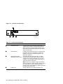
Controls and Indicators . . . . .
Console Mode . . . . . . . . . . . . .
Entering Console Mode . .
Exiting Console Mode . . .
Environment Variables . . . . . .
Booting an Operating System
Updating Firmware . . . . . . . .
.
.
.
.
.
.
.
.
.
.
.
.
.
.
.
.
.
.
.
.
.
.
.
.
.
.
.
.
.
.
.
.
.
.
.
.
.
.
.
.
.
.
.
.
.
.
.
.
.
.
.
.
.
.
.
.
.
.
.
.
.
.
.
.
.
.
.
.
.
.
.
.
.
.
.
.
.
.
.
.
.
.
.
.
.
.
.
.
.
.
.
.
.
.
.
.
.
.
.
.
.
.
.
.
.
.
.
.
.
.
.
.
.
.
.
.
.
.
.
.
.
.
.
.
.
.
.
.
.
.
.
.
.
.
.
.
.
.
.
.
.
.
.
.
.
.
.
.
.
.
.
.
.
.
3–1
3–3
3–3
3–3
3–3
3–7
3–7
Overview . . . . . . . . . . . . . . . . . . . . . . . . . . . . . . . .
Operating Environments . . . . . . . . . . . . . . . . . . . .
POST Diagnostics . . . . . . . . . . . . . . . . . . . . . .
Console Prompt Diagnostics . . . . . . . . . . . . . . .
Diagnostic Test Descriptions . . . . . . . . . . . . . . . . .
Available Console Diagnostics . . . . . . . . . . . . .
SROM Initialization Countdown . . . . . . . . . . .
Console POST Descriptions . . . . . . . . . . . . . . .
POST Non-Volatile RAM Diagnostic . . . . . . . . . . .
POST Memory Diagnostic . . . . . . . . . . . . . . . . . . .
Console Diagnostic Test Descriptions . . . . . . . .
Heartbeat Timer Test . . . . . . . . . . . . . . . . . . . . . . .
Interval Timer Tests . . . . . . . . . . . . . . . . . . . . . . .
DECchip 21040 Ethernet Controller Tests . . . . . . .
DALLAS DS1386 RAMified Watchdog Timekeeper
Tests . . . . . . . . . . . . . . . . . . . . . . . . . . . . . . . . . . . .
Local Area Network Address ROM Test . . . . . . . . .
NCR 53C810 PCI-SCSI I/O Processor Tests . . . . . .
Watchdog Timer Interrupt Test . . . . . . . . . . . . . . .
VME Interface Tests . . . . . . . . . . . . . . . . . . . . . . .
Initialization Sequence . . . . . . . . . . . . . . . . . . . . . .
.
.
.
.
.
.
.
.
.
.
.
.
.
.
.
.
.
.
.
.
.
.
.
.
.
.
.
.
.
.
.
.
.
.
.
.
.
.
.
.
.
.
.
.
.
.
.
.
.
.
.
.
.
.
.
.
.
.
.
.
.
.
.
.
.
.
.
.
.
.
.
.
.
.
.
.
.
.
.
.
.
.
.
.
4–1
4–1
4–1
4–2
4–2
4–2
4–4
4–5
4–6
4–7
4–8
4–9
4–10
4–16
.
.
.
.
.
.
.
.
.
.
.
.
.
.
.
.
.
.
.
.
.
.
.
.
.
.
.
.
.
.
.
.
.
.
.
.
4–18
4–22
4–24
4–27
4–28
4–30
4 Diagnostics
4.1
4.2
4.2.1
4.2.2
4.3
4.3.1
4.3.2
4.3.3
4.3.4
4.4
iv
5 System Address Mapping
CPU Address Mapping to PCI Space . . . . . . . . . . . . .
Cacheable Memory Space (0x000000000 to
0x0FFFFFFFF) . . . . . . . . . . . . . . . . . . . . . . . . . .
5.1.2
Noncacheable Memory Space (0x100000000 to
0x17FFFFFFF) . . . . . . . . . . . . . . . . . . . . . . . . . .
5.1.3
DECchip 21071-CA CSR Space (0x180000000 to
0x19FFFFFFF) . . . . . . . . . . . . . . . . . . . . . . . . . .
5.1.4
DECchip 21071-DA CSR Space (0x1A0000000 to
0x1AFFFFFFF) . . . . . . . . . . . . . . . . . . . . . . . . . .
5.1.5
PCI Interrupt Acknowledge/Special Cycle Space
(0x1B0000000 to 0x1BFFFFFFF) . . . . . . . . . . . . .
5.1.6
PCI Sparse I/O Space (0x1C0000000 to
0x1DFFFFFFF) . . . . . . . . . . . . . . . . . . . . . . . . . .
5.1.7
PCI Configuration Space (0x1E0000000 to
0x1FFFFFFFF) . . . . . . . . . . . . . . . . . . . . . . . . . .
5.1.7.1
PCI Configuration Cycles to Primary Bus
Targets . . . . . . . . . . . . . . . . . . . . . . . . . . . . . .
5.1.7.2
PCI Configuration Cycles to Secondary Bus
Targets . . . . . . . . . . . . . . . . . . . . . . . . . . . . . .
5.1.8
PCI Sparse Memory Space (0x200000000 to
0x2FFFFFFFF) . . . . . . . . . . . . . . . . . . . . . . . . . .
5.1.9
PCI Dense Memory Space (0x300000000 to
0x3FFFFFFFF) . . . . . . . . . . . . . . . . . . . . . . . . . .
5.2
PCI-to-Physical Memory Addressing . . . . . . . . . . . . .
5.1
5.1.1
....
5–1
....
5–4
....
5–4
....
5–4
....
5–5
....
5–5
....
5–5
....
5–8
....
5–9
....
5–10
....
5–11
....
....
5–14
5–15
6 Cache and Memory Subsystem
6.1
6.1.1
6.1.2
6.1.3
6.2
6.3
6.3.1
6.3.2
6.3.3
6.3.4
6.3.5
6.3.6
6.3.7
6.4
System Bus Interface . . . . . . . . . . . .
Arbitration on the System Bus . .
System Bus Controller . . . . . . . .
Decoding Addresses . . . . . . . . . .
Bcache Control . . . . . . . . . . . . . . . . .
Memory Controller . . . . . . . . . . . . . .
Memory Organization . . . . . . . .
Memory Address Generation . . .
Support for Memory Page Mode
Minimizing Read Latency . . . . .
Transaction Scheduler . . . . . . . .
Programmable Memory Timing .
Presence Detect Logic . . . . . . . .
Error Handling . . . . . . . . . . . . . . . .
.
.
.
.
.
.
.
.
.
.
.
.
.
.
.
.
.
.
.
.
.
.
.
.
.
.
.
.
.
.
.
.
.
.
.
.
.
.
.
.
.
.
.
.
.
.
.
.
.
.
.
.
.
.
.
.
.
.
.
.
.
.
.
.
.
.
.
.
.
.
.
.
.
.
.
.
.
.
.
.
.
.
.
.
.
.
.
.
.
.
.
.
.
.
.
.
.
.
.
.
.
.
.
.
.
.
.
.
.
.
.
.
.
.
.
.
.
.
.
.
.
.
.
.
.
.
.
.
.
.
.
.
.
.
.
.
.
.
.
.
.
.
.
.
.
.
.
.
.
.
.
.
.
.
.
.
.
.
.
.
.
.
.
.
.
.
.
.
.
.
.
.
.
.
.
.
.
.
.
.
.
.
.
.
.
.
.
.
.
.
.
.
.
.
.
.
.
.
.
.
.
.
.
.
.
.
.
.
.
.
.
.
.
.
.
.
.
.
.
.
.
.
.
.
.
.
.
.
.
.
.
.
.
.
.
.
.
.
6–4
6–4
6–4
6–4
6–5
6–5
6–6
6–7
6–7
6–7
6–7
6–7
6–8
6–8
v
6.5
Address Space of Control/Status Registers . . . . . . . .
6.6
Description of CSRs . . . . . . . . . . . . . . . . . . . . . . . . .
6.6.1
General Control Register . . . . . . . . . . . . . . . . . .
6.6.2
Error and Diagnostic Status Register . . . . . . . .
6.6.3
Tag Enable Register . . . . . . . . . . . . . . . . . . . . . .
6.6.4
Error Low Address Register . . . . . . . . . . . . . . . .
6.6.5
Error High Address Register . . . . . . . . . . . . . . .
6.6.6
LDx_L Low Address Register . . . . . . . . . . . . . . .
6.6.7
LDx_L High Address Register . . . . . . . . . . . . . .
6.6.8
Memory Control Registers . . . . . . . . . . . . . . . . .
6.6.8.1
Presence Detect Low-Data Register . . . . . . .
6.6.8.2
Presence Detect High-Data Register . . . . . .
6.6.8.3
Base Address Registers . . . . . . . . . . . . . . . .
6.6.8.4
Configuration Registers . . . . . . . . . . . . . . . .
6.6.8.5
Bank Set Timing Registers . . . . . . . . . . . . .
6.6.8.6
Global Timing Register . . . . . . . . . . . . . . . .
6.6.8.7
Refresh Timing Register . . . . . . . . . . . . . . .
6.7
Data Path . . . . . . . . . . . . . . . . . . . . . . . . . . . . . . . .
6.7.1
Memory Read Buffer . . . . . . . . . . . . . . . . . . . . .
6.7.2
I/O Read Buffer and Merge Buffer . . . . . . . . . . .
6.7.3
I/O Write and DMA Read Buffer . . . . . . . . . . . .
6.7.4
DMA Write Buffer . . . . . . . . . . . . . . . . . . . . . . .
6.7.5
Memory Write Buffer . . . . . . . . . . . . . . . . . . . . .
6.7.6
Error Handling . . . . . . . . . . . . . . . . . . . . . . . . .
.
.
.
.
.
.
.
.
.
.
.
.
.
.
.
.
.
.
.
.
.
.
.
.
.
.
.
.
.
.
.
.
.
.
.
.
.
.
.
.
.
.
.
.
.
.
.
.
.
.
.
.
.
.
.
.
.
.
.
.
.
.
.
.
.
.
.
.
.
.
.
.
.
.
.
.
.
.
.
.
.
.
.
.
.
.
.
.
.
.
.
.
.
.
.
.
.
.
.
.
.
.
.
.
.
.
.
.
.
.
.
.
.
.
.
.
.
.
.
.
6–8
6–11
6–11
6–13
6–16
6–18
6–19
6–19
6–20
6–20
6–20
6–21
6–21
6–22
6–24
6–27
6–28
6–30
6–31
6–31
6–31
6–31
6–32
6–32
Interface to the System Bus . . . . . . . . . . . . . . . . . . . . .
Decoding Physical Addresses . . . . . . . . . . . . . . . . .
Buffering System Bus Transactions . . . . . . . . . . . .
Burst Length and Prefetching for the System Bus .
Interface to the PCI bus . . . . . . . . . . . . . . . . . . . . . . . .
Decoding PCI Addresses . . . . . . . . . . . . . . . . . . . .
Buffering PCI Transactions . . . . . . . . . . . . . . . . . .
Burst Length and Prefetching for PCI bus . . . . . . .
Features . . . . . . . . . . . . . . . . . . . . . . . . . . . . . . . . . . . .
Burst Order . . . . . . . . . . . . . . . . . . . . . . . . . . . . . .
Parity Support . . . . . . . . . . . . . . . . . . . . . . . . . . .
Data Coherency . . . . . . . . . . . . . . . . . . . . . . . . . . .
Interrupts . . . . . . . . . . . . . . . . . . . . . . . . . . . . . . .
Exclusive Access . . . . . . . . . . . . . . . . . . . . . . . . .
Bus Parking . . . . . . . . . . . . . . . . . . . . . . . . . . . . . .
Retry Timeout . . . . . . . . . . . . . . . . . . . . . . . . . . . .
.
.
.
.
.
.
.
.
.
.
.
.
.
.
.
.
.
.
.
.
.
.
.
.
.
.
.
.
.
.
.
.
.
.
.
.
.
.
.
.
.
.
.
.
.
.
.
.
7–2
7–2
7–3
7–3
7–3
7–3
7–3
7–4
7–4
7–4
7–4
7–5
7–6
7–6
7–6
7–7
7 PCI Host Bridge
7.1
7.1.1
7.1.2
7.1.3
7.2
7.2.1
7.2.2
7.2.3
7.3
7.3.1
7.3.2
7.3.3
7.3.4
7.3.5
7.3.6
7.3.7
vi
7.3.8
PCI Master Timeout . . . . . . . . . . . . . . . . .
7.3.9
Address Stepping in Configuration Cycles .
7.4
Address Space of Control/Status Registers . . . .
7.5
Description of CSRs . . . . . . . . . . . . . . . . . . . . .
7.5.1
Diagnostic Control/Status Register . . . . . .
7.5.2
PCI Error Address Register . . . . . . . . . . . .
7.5.3
System Bus Error Address Register . . . . . .
7.5.4
Dummy Registers 1 Through 3 . . . . . . . . .
7.5.5
Translated Base Registers 1 and 2 . . . . . . .
7.5.6
PCI Base Registers 1 and 2 . . . . . . . . . . . .
7.5.7
PCI Mask Registers 1 and 2 . . . . . . . . . . .
7.5.8
Host Address Extension Register 0 . . . . . .
7.5.9
Host Address Extension Register 1 . . . . . .
7.5.10
Host Address Extension Register 2 . . . . . .
7.5.11
PCI Master Latency Timer Register . . . . . .
7.5.12
TLB Tag Registers 0 Through 7 . . . . . . . . .
7.5.13
TLB Data Registers 0 Through 7 . . . . . . . .
7.5.14
Translation Buffer Invalidate All Register:
0x1A0000400 . . . . . . . . . . . . . . . . . . . . . . .
.
.
.
.
.
.
.
.
.
.
.
.
.
.
.
.
.
.
.
.
.
.
.
.
.
.
.
.
.
.
.
.
.
.
.
.
.
.
.
.
.
.
.
.
.
.
.
.
.
.
.
.
.
.
.
.
.
.
.
.
.
.
.
.
.
.
.
.
.
.
.
.
.
.
.
.
.
.
.
.
.
.
.
.
.
.
.
.
.
.
.
.
.
.
.
.
.
.
.
.
.
.
.
.
.
.
.
.
.
.
.
.
.
.
.
.
.
.
.
.
.
.
.
.
.
.
.
.
.
.
.
.
.
.
.
.
.
.
.
.
.
.
.
.
.
.
.
.
.
.
.
.
.
7–7
7–7
7–7
7–9
7–9
7–13
7–14
7–15
7–15
7–16
7–17
7–18
7–18
7–19
7–20
7–20
7–21
.........
7–22
.
.
.
.
.
.
.
.
.
.
.
.
.
.
.
.
.
.
.
.
.
.
.
.
.
.
.
.
.
.
.
.
.
.
.
.
.
.
.
.
.
.
.
.
.
.
.
.
.
.
.
.
.
.
.
.
.
.
.
.
.
.
.
.
.
.
.
.
.
.
.
.
.
.
.
.
.
.
.
.
.
.
.
.
.
.
.
.
.
.
.
.
.
.
.
.
.
.
.
.
.
.
.
.
.
.
.
.
8–3
8–3
8–4
8–5
8–6
8–6
8–6
8–7
8–7
8–7
8–8
8–11
9.1
Nbus Address Space . . . . . . . . . . . . . . . . . . . . . .
9.1.1
SIO Chip PCI Configuration Space . . . . . . .
9.1.1.1
PCI Control Register . . . . . . . . . . . . . . .
9.1.1.2
ISA Controller Recovery Timer Register
9.1.1.3
ISA Clock Divisor Register . . . . . . . . . . .
9.2
Module Registers . . . . . . . . . . . . . . . . . . . . . . . .
.
.
.
.
.
.
.
.
.
.
.
.
.
.
.
.
.
.
.
.
.
.
.
.
.
.
.
.
.
.
.
.
.
.
.
.
.
.
.
.
.
.
.
.
.
.
.
.
9–1
9–2
9–3
9–4
9–4
9–4
8 PCI bus
8.1
8.1.1
8.1.2
8.1.3
8.1.4
8.2
8.2.1
8.2.2
8.2.3
8.2.4
8.2.5
8.3
Ethernet Controller . . . . . . . . . . .
PCI Configuration Registers .
Ethernet Controller CSRs . . .
PCI Cycles . . . . . . . . . . . . . . .
Ethernet Address . . . . . . . . . .
SCSI Controller . . . . . . . . . . . . . .
Connection and Termination .
SCSI ID . . . . . . . . . . . . . . . . .
Programming . . . . . . . . . . . . .
PCI Configuration Registers .
SCSI Control Status Registers
PCI I/O Companion Card . . . . . . .
.
.
.
.
.
.
.
.
.
.
.
.
.
.
.
.
.
.
.
.
.
.
.
.
.
.
.
.
.
.
.
.
.
.
.
.
.
.
.
.
.
.
.
.
.
.
.
.
.
.
.
.
.
.
.
.
.
.
.
.
.
.
.
.
.
.
.
.
.
.
.
.
.
.
.
.
.
.
.
.
.
.
.
.
.
.
.
.
.
.
.
.
.
.
.
.
.
.
.
.
.
.
.
.
.
.
.
.
.
.
.
.
.
.
.
.
.
.
.
.
9 Nbus
vii
9.2.1
9.2.2
9.2.3
9.2.4
9.2.5
9.2.6
9.2.7
9.2.8
9.3
9.4
9.4.1
9.4.2
9.5
9.6
9.6.1
9.6.2
9.7
9.7.1
9.7.2
9.7.3
9.7.4
9.7.5
9.8
9.9
Module Display Control Register . . . . . . . . . . . . . . . .
Module Configuration Register . . . . . . . . . . . . . . . . . . .
Interrupt and Interrupt Mask Registers 1, 2, 3, 4 . . . .
Memory Configuration Registers 0, 1, 2, 3 and Memory
Identification Register . . . . . . . . . . . . . . . . . . . . . . . . .
Reset Reason Registers . . . . . . . . . . . . . . . . . . . . . . . .
Heartbeat Register . . . . . . . . . . . . . . . . . . . . . . . . . . . .
Module Control Register 1 . . . . . . . . . . . . . . . . . . . . .
Bcache Configuration Register . . . . . . . . . . . . . . . . . . .
ROM . . . . . . . . . . . . . . . . . . . . . . . . . . . . . . . . . . . . . . . . .
Super I/O Chip . . . . . . . . . . . . . . . . . . . . . . . . . . . . . . . . . .
Serial Port Channels A and B . . . . . . . . . . . . . . . . . . .
Super I/O Register Address Space . . . . . . . . . . . . . . . .
Keyboard and Mouse Controller . . . . . . . . . . . . . . . . . . . . .
TOY Clock . . . . . . . . . . . . . . . . . . . . . . . . . . . . . . . . . . . . .
TOY Clock Timekeeping Registers . . . . . . . . . . . . . . . .
TOY Clock Command Register . . . . . . . . . . . . . . . . . . .
Interval Timing Registers . . . . . . . . . . . . . . . . . . . . . . . . .
Interval Timing Control Register . . . . . . . . . . . . . . . . .
Timer Registers . . . . . . . . . . . . . . . . . . . . . . . . . . . . . .
Timer Modes . . . . . . . . . . . . . . . . . . . . . . . . . . . . . . . .
Interrupts . . . . . . . . . . . . . . . . . . . . . . . . . . . . . . . . . .
Timer Interrupt Status Registers . . . . . . . . . . . . . . . . .
Watchdog Timer . . . . . . . . . . . . . . . . . . . . . . . . . . . . . . . . .
Nonvolatile RAM . . . . . . . . . . . . . . . . . . . . . . . . . . . . . . . .
9–5
9–6
9–8
9–8
9–12
9–14
9–14
9–16
9–17
9–18
9–18
9–19
9–21
9–22
9–23
9–24
9–25
9–26
9–28
9–29
9–31
9–32
9–33
9–36
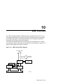
10 VME Interface
10.1
VMEbus Master . . . . . . . . . . . . . . . . . .
10.1.1
Outbound Scatter-Gather Mapping
10.1.1.1
Address Modifier . . . . . . . . . . .
10.1.1.2
Read-Modify-Write . . . . . . . . . .
10.1.2
Data Transfers . . . . . . . . . . . . . . . .
10.1.2.1
Single Mode Transfers . . . . . . .
10.1.2.2
Block Mode Transfers . . . . . . . .
10.1.3
Requesting the VMEbus . . . . . . . . .
10.2
VMEbus Slave . . . . . . . . . . . . . . . . . .
10.2.1
Decoding Addresses . . . . . . . . . . .
10.2.2
Inbound Scatter-Gather Entries . . .
viii
.
.
.
.
.
.
.
.
.
.
.
.
.
.
.
.
.
.
.
.
.
.
.
.
.
.
.
.
.
.
.
.
.
.
.
.
.
.
.
.
.
.
.
.
.
.
.
.
.
.
.
.
.
.
.
.
.
.
.
.
.
.
.
.
.
.
.
.
.
.
.
.
.
.
.
.
.
.
.
.
.
.
.
.
.
.
.
.
.
.
.
.
.
.
.
.
.
.
.
.
.
.
.
.
.
.
.
.
.
.
.
.
.
.
.
.
.
.
.
.
.
.
.
.
.
.
.
.
.
.
.
.
.
.
.
.
.
.
.
.
.
.
.
.
.
.
.
.
.
.
.
.
.
.
.
.
.
.
.
.
.
.
.
.
.
10–2
10–4
10–6
10–6
10–7
10–7
10–7
10–9
10–9
10–10
10–12
Interprocessor Communication . . . . . . . . . . . . . . . . . . .
Interprocessor Communication Registers . . . . . . . .
Interprocessor Communication Global Switches . . .
Interprocessor Communication Module
Switches . . . . . . . . . . . . . . . . . . . . . . . . . . . . . . . . .
10.3
System Controller Operation . . . . . . . . . . . . . . . . . . . . . . .
10.3.1
Arbitrating the VMEbus . . . . . . . . . . . . . . . . . . . . . . .
10.3.1.1
Requesting the VMEbus . . . . . . . . . . . . . . . . . . . . .
10.3.1.2
Releasing the VMEbus . . . . . . . . . . . . . . . . . . . . . .
10.3.2
System Clock Output . . . . . . . . . . . . . . . . . . . . . . . . . .
10.3.3
Timeout Timers . . . . . . . . . . . . . . . . . . . . . . . . . . . . . .
10.3.3.1
Arbitration Timers . . . . . . . . . . . . . . . . . . . . . . . . .
10.3.3.2
VMEbus Transfer Timers . . . . . . . . . . . . . . . . . . . .
10.3.3.3
Local Bus Transfer Timer . . . . . . . . . . . . . . . . . . .
10.3.4
VMEbus Interrupt Handling . . . . . . . . . . . . . . . . . . . .
10.4
Byte Swapping . . . . . . . . . . . . . . . . . . . . . . . . . . . . . . . . . .
10.4.1
DC7407 Byte Swapping . . . . . . . . . . . . . . . . . . . . . . . .
10.4.2
VIC64 Byte Swapping . . . . . . . . . . . . . . . . . . . . . . . . .
10.5
Initializing the VME Interface . . . . . . . . . . . . . . . . . . . . . .
10.5.1
VME PCI Configuration Registers . . . . . . . . . . . . . . . .
10.5.2
Programming Scatter-Gather RAM . . . . . . . . . . . . . . .
10.5.3
Configuring the VIC64 . . . . . . . . . . . . . . . . . . . . . . . . .
10.6
Summary of VME Interface Registers . . . . . . . . . . . . . . . .
10.7
VME Subsystem Restrictions (as of 03-Jun-94) . . . . . . . . .
10.7.1
Collision of VIC64 Master Write Posting with Master
Block Transfers . . . . . . . . . . . . . . . . . . . . . . . . . . . . . .
10.7.2
VIC64 Errata: A16 Master Cycles During
Interleave . . . . . . . . . . . . . . . . . . . . . . . . . . . . . . . . . . .
10.2.3
10.2.3.1
10.2.3.2
10.2.3.3
10–14
10–14
10–14
10–15
10–17
10–18
10–18
10–19
10–21
10–21
10–21
10–22
10–23
10–23
10–26
10–26
10–27
10–30
10–30
10–31
10–32
10–37
10–40
10–40
10–40
11 System Interrupts
11.1
System Interrupts . . . . . . . . . . . . . . . . . . . . . . . . . . . . . . .
11.1.1
Xilinx Interrupt Controller . . . . . . . . . . . . . . . . . . . . . .
11.1.2
VIC64 Chip System Interrupt Controller . . . . . . . . . . .
11.1.2.1
Basic Operation . . . . . . . . . . . . . . . . . . . . . . . . . . .
11.1.3
VIC64 Chip Interrupt Sources . . . . . . . . . . . . . . . . . . .
11.1.3.1
Local Device Interrupts . . . . . . . . . . . . . . . . . . . . .
11.1.3.2
VMEbus Interrupt Requests . . . . . . . . . . . . . . . . .
11.1.3.3
Status/Error Interrupts . . . . . . . . . . . . . . . . . . . . .
11.1.4
SIO Chip Programmable Interrupt Controller . . . . . . .
11.1.4.1
Nonmaskable System Events . . . . . . . . . . . . . . . . .
11.1.4.2
NMI Status and Control Register . . . . . . . . . . . . .
11.1.4.3
EPIC Interrupt . . . . . . . . . . . . . . . . . . . . . . . . . . .
11–1
11–2
11–4
11–5
11–6
11–6
11–7
11–8
11–11
11–11
11–12
11–13
ix
11.2
Module Reset . . . . . . . . . . . . . . . . . . . . . . . . . . . . . . . . . . .
11–13
12 Console Primer
12.1
12.1.1
12.1.2
12.1.3
12.1.4
12.2
12.3
12.4
12.4.1
12.4.2
12.5
12.6
12.7
12.7.1
12.7.2
12.8
12.9
About the Console . . . . . . . . . . . . . . . . . . . . . . . . . . . . . . .
Console Features . . . . . . . . . . . . . . . . . . . . . . . . . . . .
Command Overview . . . . . . . . . . . . . . . . . . . . . . . . . .
Shell Operators . . . . . . . . . . . . . . . . . . . . . . . . . . . . . .
Using Flow Control . . . . . . . . . . . . . . . . . . . . . . . . . . .
Getting Information About the System . . . . . . . . . . . . . . .
Getting Help . . . . . . . . . . . . . . . . . . . . . . . . . . . . . . . . . . .
Examining and Depositing to Memory or System Registers
..............................................
Accessing Memory . . . . . . . . . . . . . . . . . . . . . . . . . . . .
Examining Registers . . . . . . . . . . . . . . . . . . . . . . . . . .
Using Pipes and grep to Filter Output . . . . . . . . . . . . . . . .
Using I/O Redirection (>) . . . . . . . . . . . . . . . . . . . . . . . . .
Running Commands in Background . . . . . . . . . . . . . . . . .
Monitoring Status . . . . . . . . . . . . . . . . . . . . . . . . . . . .
Killing a Process . . . . . . . . . . . . . . . . . . . . . . . . . . . . .
Creating Scripts . . . . . . . . . . . . . . . . . . . . . . . . . . . . . . . .
Copying Scripts Over the Network . . . . . . . . . . . . . . . . . .
12–1
12–1
12–2
12–3
12–4
12–5
12–6
12–7
12–9
12–10
12–12
12–12
12–13
12–13
12–14
12–14
12–15
13 Console Commands
13.1
Console Commands . . . . . . . . . . . .
13.1.1
Special Keys . . . . . . . . . . . . . . .
13.1.2
Command Line Characteristics
13.1.3
Radix Control . . . . . . . . . . . . . .
13.1.4
Console Command Dictionary .
alloc . . . . . . . . . . . . . . . . . . . . . . .
boot . . . . . . . . . . . . . . . . . . . . . . . .
break . . . . . . . . . . . . . . . . . . . . . . .
cat . . . . . . . . . . . . . . . . . . . . . . . . .
chmod . . . . . . . . . . . . . . . . . . . . . .
chown . . . . . . . . . . . . . . . . . . . . . .
clear . . . . . . . . . . . . . . . . . . . . . . .
clear_log . . . . . . . . . . . . . . . . . . . .
date . . . . . . . . . . . . . . . . . . . . . . . .
deposit . . . . . . . . . . . . . . . . . . . . .
dynamic . . . . . . . . . . . . . . . . . . . .
x
.
.
.
.
.
.
.
.
.
.
.
.
.
.
.
.
.
.
.
.
.
.
.
.
.
.
.
.
.
.
.
.
.
.
.
.
.
.
.
.
.
.
.
.
.
.
.
.
.
.
.
.
.
.
.
.
.
.
.
.
.
.
.
.
.
.
.
.
.
.
.
.
.
.
.
.
.
.
.
.
.
.
.
.
.
.
.
.
.
.
.
.
.
.
.
.
.
.
.
.
.
.
.
.
.
.
.
.
.
.
.
.
.
.
.
.
.
.
.
.
.
.
.
.
.
.
.
.
.
.
.
.
.
.
.
.
.
.
.
.
.
.
.
.
.
.
.
.
.
.
.
.
.
.
.
.
.
.
.
.
.
.
.
.
.
.
.
.
.
.
.
.
.
.
.
.
.
.
.
.
.
.
.
.
.
.
.
.
.
.
.
.
.
.
.
.
.
.
.
.
.
.
.
.
.
.
.
.
.
.
.
.
.
.
.
.
.
.
.
.
.
.
.
.
.
.
.
.
.
.
.
.
.
.
.
.
.
.
.
.
.
.
.
.
.
.
.
.
.
.
.
.
.
.
.
.
.
.
.
.
.
.
.
.
.
.
.
.
.
.
.
.
.
.
.
.
.
.
.
.
.
.
.
.
.
.
.
.
13–1
13–1
13–2
13–2
13–3
13–4
13–6
13–14
13–15
13–16
13–18
13–19
13–20
13–21
13–23
13–28
echo . . . . . . . . .
eval . . . . . . . . .
examine . . . . .
exer . . . . . . . . .
exit . . . . . . . . .
false . . . . . . . .
free . . . . . . . . .
grep . . . . . . . . .
hd . . . . . . . . . .
help . . . . . . . . .
init_ev . . . . . . .
initialize . . . . .
kill . . . . . . . . .
line . . . . . . . . .
ls . . . . . . . . . . .
memexer . . . . .
memtest . . . . .
net . . . . . . . . .
ps . . . . . . . . . .
pwrup . . . . . . .
rm . . . . . . . . . .
sa . . . . . . . . . .
semaphore . . . .
set . . . . . . . . . .
set led . . . . . . .
set reboot srom
set toy sleep . .
sh . . . . . . . . . .
show . . . . . . . .
show config . . .
show device . . .
show hwrpb . . .
show led . . . . .
show map . . . .
show_log . . . . .
sleep . . . . . . . .
sort . . . . . . . . .
.
.
.
.
.
.
.
.
.
.
.
.
.
.
.
.
.
.
.
.
.
.
.
.
.
.
.
.
.
.
.
.
.
.
.
.
.
.
.
.
.
.
.
.
.
.
.
.
.
.
.
.
.
.
.
.
.
.
.
.
.
.
.
.
.
.
.
.
.
.
.
.
.
.
.
.
.
.
.
.
.
.
.
.
.
.
.
.
.
.
.
.
.
.
.
.
.
.
.
.
.
.
.
.
.
.
.
.
.
.
.
.
.
.
.
.
.
.
.
.
.
.
.
.
.
.
.
.
.
.
.
.
.
.
.
.
.
.
.
.
.
.
.
.
.
.
.
.
.
.
.
.
.
.
.
.
.
.
.
.
.
.
.
.
.
.
.
.
.
.
.
.
.
.
.
.
.
.
.
.
.
.
.
.
.
.
.
.
.
.
.
.
.
.
.
.
.
.
.
.
.
.
.
.
.
.
.
.
.
.
.
.
.
.
.
.
.
.
.
.
.
.
.
.
.
.
.
.
.
.
.
.
.
.
.
.
.
.
.
.
.
.
.
.
.
.
.
.
.
.
.
.
.
.
.
.
.
.
.
.
.
.
.
.
.
.
.
.
.
.
.
.
.
.
.
.
.
.
.
.
.
.
.
.
.
.
.
.
.
.
.
.
.
.
.
.
.
.
.
.
.
.
.
.
.
.
.
.
.
.
.
.
.
.
.
.
.
.
.
.
.
.
.
.
.
.
.
.
.
.
.
.
.
.
.
.
.
.
.
.
.
.
.
.
.
.
.
.
.
.
.
.
.
.
.
.
.
.
.
.
.
.
.
.
.
.
.
.
.
.
.
.
.
.
.
.
.
.
.
.
.
.
.
.
.
.
.
.
.
.
.
.
.
.
.
.
.
.
.
.
.
.
.
.
.
.
.
.
.
.
.
.
.
.
.
.
.
.
.
.
.
.
.
.
.
.
.
.
.
.
.
.
.
.
.
.
.
.
.
.
.
.
.
.
.
.
.
.
.
.
.
.
.
.
.
.
.
.
.
.
.
.
.
.
.
.
.
.
.
.
.
.
.
.
.
.
.
.
.
.
.
.
.
.
.
.
.
.
.
.
.
.
.
.
.
.
.
.
.
.
.
.
.
.
.
.
.
.
.
.
.
.
.
.
.
.
.
.
.
.
.
.
.
.
.
.
.
.
.
.
.
.
.
.
.
.
.
.
.
.
.
.
.
.
.
.
.
.
.
.
.
.
.
.
.
.
.
.
.
.
.
.
.
.
.
.
.
.
.
.
.
.
.
.
.
.
.
.
.
.
.
.
.
.
.
.
.
.
.
.
.
.
.
.
.
.
.
.
.
.
.
.
.
.
.
.
.
.
.
.
.
.
.
.
.
.
.
.
.
.
.
.
.
.
.
.
.
.
.
.
.
.
.
.
.
.
.
.
.
.
.
.
.
.
.
.
.
.
.
.
.
.
.
.
.
.
.
.
.
.
.
.
.
.
.
.
.
.
.
.
.
.
.
.
.
.
.
.
.
.
.
.
.
.
.
.
.
.
.
.
.
.
.
.
.
.
.
.
.
.
.
.
.
.
.
.
.
.
.
.
.
.
.
.
.
.
.
.
.
.
.
.
.
.
.
.
.
.
.
.
.
.
.
.
.
.
.
.
.
.
.
.
.
.
.
.
.
.
.
.
.
.
.
.
.
.
.
.
.
.
.
.
.
.
.
.
.
.
.
.
.
.
.
.
.
.
.
.
.
.
.
.
.
.
.
.
.
.
.
.
.
.
.
.
.
.
.
.
.
.
.
.
.
.
.
.
.
.
.
.
.
.
.
.
.
.
.
.
.
.
.
.
.
.
.
.
.
.
.
.
.
.
.
.
.
.
.
.
.
.
.
.
.
.
.
.
.
.
.
.
.
.
.
.
.
.
.
.
.
.
.
.
.
.
.
.
.
.
.
.
.
.
.
.
.
.
.
.
.
.
.
.
.
.
.
.
.
.
.
.
.
.
.
.
.
.
.
.
.
.
.
.
.
.
.
.
.
.
.
.
.
.
.
.
.
.
.
.
.
.
.
.
.
.
.
.
.
.
.
.
.
.
.
.
.
.
.
.
.
.
.
.
.
.
.
.
.
.
.
.
.
.
.
.
.
.
.
.
.
.
.
.
.
.
.
.
.
.
.
.
.
.
.
.
.
.
.
.
.
.
.
.
.
.
.
.
.
.
.
.
.
.
.
.
.
.
.
.
.
.
.
.
.
.
.
.
.
.
.
.
.
.
.
.
.
.
.
.
.
.
.
.
.
.
.
.
.
.
.
.
.
.
.
.
.
.
.
.
.
.
.
.
.
.
.
.
.
.
.
.
.
.
.
.
.
.
.
.
.
.
.
.
.
.
.
.
.
.
.
.
.
.
.
.
.
.
.
.
.
.
.
.
.
.
.
.
.
.
.
.
.
.
.
.
.
.
.
.
.
.
.
.
.
.
.
.
.
.
.
.
.
.
.
.
.
.
.
.
.
.
.
.
.
.
.
.
.
.
.
.
.
.
.
.
.
.
.
.
.
.
.
.
.
.
.
.
.
.
.
.
.
.
.
.
.
.
.
.
.
.
.
.
.
.
.
.
.
.
.
.
.
.
.
.
.
.
.
.
.
.
.
.
.
.
.
.
.
.
.
.
.
.
.
.
.
.
.
.
.
.
.
.
.
.
.
.
.
.
.
.
.
.
.
.
.
.
.
.
.
.
.
13–30
13–32
13–34
13–40
13–49
13–50
13–51
13–52
13–55
13–57
13–59
13–60
13–61
13–62
13–63
13–64
13–65
13–72
13–75
13–76
13–77
13–78
13–79
13–80
13–83
13–84
13–85
13–86
13–88
13–90
13–91
13–93
13–94
13–95
13–96
13–98
13–99
xi
sp . . .
start .
stop . .
update
.
.
.
.
.
.
.
.
.
.
.
.
.
.
.
.
.
.
.
.
.
.
.
.
.
.
.
.
.
.
.
.
.
.
.
.
.
.
.
.
.
.
.
.
.
.
.
.
.
.
.
.
.
.
.
.
.
.
.
.
.
.
.
.
.
.
.
.
.
.
.
.
.
.
.
.
.
.
.
.
.
.
.
.
.
.
.
.
.
.
.
.
.
.
.
.
.
.
.
.
.
.
.
.
.
.
.
.
.
.
.
.
.
.
.
.
.
.
.
.
.
.
.
.
.
.
.
.
.
.
.
.
.
.
.
.
.
.
.
.
.
.
.
.
.
.
.
.
.
.
.
.
.
.
.
.
.
.
.
.
13–100
13–101
13–102
13–103
CPU Connector Pinouts . . . . . . . . . . . . . . . . . . . . .
I/O Type 1 Card Connector Pinouts . . . . . . . . . . . .
VMEbus (J1) Connector Pinouts . . . . . . . . . . .
Console (J6) and Serial (J7) Connector Pinouts
Ethernet (J9) Connector Pinouts . . . . . . . . . . .
Primary Breakout Module Connector Pinouts . . . .
Secondary Breakout Module Connector Pinouts . . .
Keyboard and Mouse (J1) Connector Pinouts . .
Parallel Port (J6) Connector Pinouts . . . . . . . .
PMC I/O Companion Card Connector Pinouts . . . .
.
.
.
.
.
.
.
.
.
.
.
.
.
.
.
.
.
.
.
.
.
.
.
.
.
.
.
.
.
.
.
.
.
.
.
.
.
.
.
.
.
.
.
.
.
.
.
.
.
.
.
.
.
.
.
.
.
.
.
.
A–1
A–1
A–2
A–3
A–4
A–4
A–6
A–7
A–8
A–9
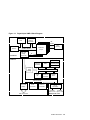
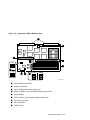
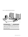
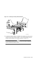
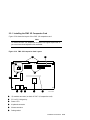
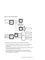
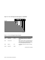
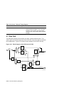
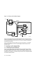
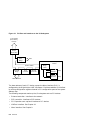
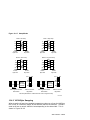
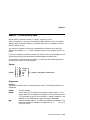
Digital Alpha VME 4 Block Diagram . . . . . . . . . . . . .
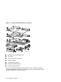
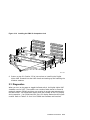
Digital Alpha VME 4 Module Components . . . . . . . . .
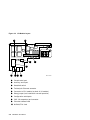
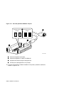
Digital Alpha VME 4 Module Layout . . . . . . . . . . . . .
I/O Module Layout . . . . . . . . . . . . . . . . . . . . . . . . . . .
Installing the Main Memory Modules . . . . . . . . . . . .
Cache Memory Modules . . . . . . . . . . . . . . . . . . . . . . .
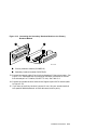
Installing the Digital Alpha VME 4 Module . . . . . . . .
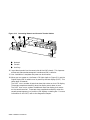
Alpha VME 4 Primary Breakout Module . . . . . . . . . .
Primary Breakout Module Jumpers . . . . . . . . . . . . . .
Connecting the SCSI Cable to the Primary Breakout
Module . . . . . . . . . . . . . . . . . . . . . . . . . . . . . . . . . . . .
Installing the Primary Breakout Module . . . . . . . . . .
Secondary Breakout Module Jumpers . . . . . . . . . . . .
Connecting the Secondary Breakout Module to the
Primary Breakout Module . . . . . . . . . . . . . . . . . . . .
Connecting Network and Console Terminal Cables . .
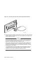
PMC I/O Companion Card Layout . . . . . . . . . . . . . . .
.
.
.
.
.
.
.
.
.
1–3
2–2
2–7
2–8
2–11
2–13
2–15
2–16
2–17
.
.
.
2–18
2–19
2–20
.
.
.
2–21
2–22
2–23
A Module Connector Pinouts
A.1
A.2
A.2.1
A.2.2
A.2.3
A.3
A.4
A.4.1
A.4.2
A.5
Index
Figures
1–1
2–1
2–2
2–3
2–4
2–5
2–6
2–7
2–8
2–9
2–10
2–11
2–12
2–13
2–14
xii
2–15
2–16
3–1
4–1
4–2
4–3
4–4
4–5
5–1
5–2
5–3
5–4
5–5
5–6
6–1
6–2
6–3
6–4
6–5
6–6
6–7
6–8
6–9
6–10
6–11
6–12
6–13
6–14
6–15
6–16
6–17
6–18
6–19
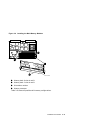
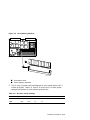
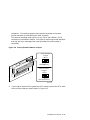
Connecting the PMC I/O Companion Card . . . . . . . . . .
Installing the PMC I/O Companion Card . . . . . . . . . . .
Controls and Indicators . . . . . . . . . . . . . . . . . . . . . . . .
Loopback Descriptions for Interval Timer Test 3 and
4. . . . . . . . . . . . . . . . . . . . . . . . . . . . . . . . . . . . . . . . . .
LAN Address ROM Format . . . . . . . . . . . . . . . . . . . . .
SROM Test Flows . . . . . . . . . . . . . . . . . . . . . . . . . . . . .
Console POST Flows . . . . . . . . . . . . . . . . . . . . . . . . . .
Console POST Flows . . . . . . . . . . . . . . . . . . . . . . . . . .
System Bus Address Map . . . . . . . . . . . . . . . . . . . . . .
PCI Sparse I/O Space Address Translation . . . . . . . . .
PCI Memory Space Address Translation . . . . . . . . . . .
PCI Target Window Compare Scheme . . . . . . . . . . . . .
Scatter-Gather Map Page Table Entry in Memory . . . .
Scatter-Gather Map Translation of PCI Bus Address to
System Bus Address . . . . . . . . . . . . . . . . . . . . . . . . . .
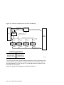
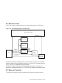
Cache and Memory Subsystem . . . . . . . . . . . . . . . . . .
Address and Data Paths of Cache and Memory . . . . . .
21071-CA Block Diagram . . . . . . . . . . . . . . . . . . . . . . .
Cache Subsystem for a 2 MB Cache . . . . . . . . . . . . . . .
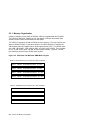
Maximum and Minimum DIMM Bank Layouts . . . . . .
General Control Register: 0x180000000 . . . . . . . . . . . .
Error and Diagnostic Status Register:
0x180000020 . . . . . . . . . . . . . . . . . . . . . . . . . . . . . . . .
Tag Enable Register: 0x180000060 . . . . . . . . . . . . . . .
Error Low Address Register: 0x180000080 . . . . . . . . .
Error High Address Register: 0x1800000A0 . . . . . . . .
LDx_L Low Address Register: 0x1800000C0 . . . . . . . .
LDx_L High Address Register: 0x1800000E0 . . . . . . .
Presence Detect Low-Data Register: 0x180000280 . . .
Presence Detect High-Data Register: 0x180000260 . . .
Bank 0 Base Address Register: 0x180000800 . . . . . . .
Configuration Registers for Bank Set 0:
0x180000A00 . . . . . . . . . . . . . . . . . . . . . . . . . . . . . . . .
Bank Set 0 Timing Register A: 0x180000C00 . . . . . . . .
Bank Set 0 Timing Register B: 0x180000E00 . . . . . . . .
Global Timing Register: 0x180000200 . . . . . . . . . . . . .
2–26
2–27
3–2
4–15
4–23
4–30
4–31
4–32
5–2
5–6
5–12
5–17
5–19
5–21
6–1
6–2
6–3
6–5
6–6
6–11
6–14
6–16
6–19
6–19
6–20
6–20
6–21
6–21
6–22
6–22
6–25
6–26
6–28
xiii
6–20
6–21
7–1
7–2
7–3
7–4
7–5
7–6
7–7
7–8
7–9
7–10
7–11
7–12
7–13
7–14
8–1
8–2
8–3
8–4
9–1
9–2
9–3
9–4
9–5
9–6
9–7
9–8
9–9
9–10
9–11
9–12
9–13
xiv
Refresh Timing Register: 0x180000220 . . . . . . . . . .
Block Diagram of the DECchip 21071-BA . . . . . . . .
PCI Host Bridge . . . . . . . . . . . . . . . . . . . . . . . . . . . .
DECchip 21071-DA Block Diagram . . . . . . . . . . . . .
Diagnostic Control/Status Register: 0x1A0000000 . .
PCI Error Address Register: 0x1A0000020 . . . . . . .
System Bus Error Address Register: 0x1A0000040 .
Translated Base Registers 1, 2: 0x1A00000C0,
0x1A00000E0 . . . . . . . . . . . . . . . . . . . . . . . . . . . . . .
PCI Base Registers 1 and 2: 0x1A0000100,
0x1A0000120 . . . . . . . . . . . . . . . . . . . . . . . . . . . . . .
PCI Mask Registers 1 and 2: 0x1A0000140,
0x1A0000160 . . . . . . . . . . . . . . . . . . . . . . . . . . . . . .
Host Address Extension Register 0: 0x1A0000180 . .
Host Address Extension Register 1: 0x1A00001A0 .
Host Address Extension Register 2: 0x1A00001C0 .
PCI Master Latency Timer Register: 0x1A00001E0 .
TLB Tag Registers 0 Through 7: 0x1A0000200 to
0x1A00002E0 . . . . . . . . . . . . . . . . . . . . . . . . . . . . . .
TLB Data Registers 0 Through 7: 0x1A0000300 to
0x1A00003E0 . . . . . . . . . . . . . . . . . . . . . . . . . . . . . .
PCI Bus and Interfaces to the I/O Subsystem . . . . .
PCI Configuration Registers . . . . . . . . . . . . . . . . . .
DECchip 21040-AA CSR9 (ENET ROM Register) . .
PCI Configuration Block . . . . . . . . . . . . . . . . . . . . .
Nbus and Nbus Resources . . . . . . . . . . . . . . . . . . . .
SIO Configuration Block . . . . . . . . . . . . . . . . . . . . .
Module Display Control Register . . . . . . . . . . . . . . .
Display Character Set . . . . . . . . . . . . . . . . . . . . . . .
Module Configuration Register . . . . . . . . . . . . . . . . .
Memory Configuration Registers 0-3 . . . . . . . . . . . .
Memory Identification Register . . . . . . . . . . . . . . . .
Reset Reason Registers . . . . . . . . . . . . . . . . . . . . . .
Module Control Register 1 . . . . . . . . . . . . . . . . . . . .
Bcache Configuration Register . . . . . . . . . . . . . . . . .
Flash ROM Layout/Addressing . . . . . . . . . . . . . . . .
TOY Clock Command Register . . . . . . . . . . . . . . . . .
82C54 Control Byte . . . . . . . . . . . . . . . . . . . . . . . . .
.
.
.
.
.
.
.
.
.
.
.
.
.
.
6–29
6–30
7–1
7–2
7–10
7–14
7–14
..
7–15
..
7–16
.
.
.
.
.
.
.
.
.
.
7–17
7–18
7–18
7–19
7–20
..
7–21
.
.
.
.
.
.
.
.
.
.
.
.
.
.
.
.
.
.
7–21
8–2
8–4
8–6
8–8
9–1
9–3
9–6
9–6
9–7
9–9
9–10
9–13
9–15
9–16
9–18
9–24
9–26
.
.
.
.
.
.
.
.
.
.
.
.
.
.
.
.
.
.
9–14
9–15
9–16
9–17
9–18
9–19
9–20
10–1
10–2
10–3
10–4
10–5
10–6
10–7
10–8
10–9
10–10
10–11
10–12
10–13
10–14
10–15
10–16
10–17
10–18
11–1
11–2
11–3
11–4
11–5
11–6
11–7
11–8
11–9
11–10
82C54 Timer Data Access . . . . . . . . . . . . . . . . . .
Timer Clocking . . . . . . . . . . . . . . . . . . . . . . . . . . .
Timer Interrupt Status Register . . . . . . . . . . . . .
Watchdog Timer Registers . . . . . . . . . . . . . . . . . .
Watchdog Timer TOY Clock Command Register .
Watchdog Timer Module Control Register . . . . . .
NVRAM Access . . . . . . . . . . . . . . . . . . . . . . . . . .
VME Interface Block Diagram . . . . . . . . . . . . . . .
Mapping Window_1 and Window_2 . . . . . . . . . . .
Mapping Pages From PCI to VME . . . . . . . . . . .
Outbound Scatter-Gather Entry . . . . . . . . . . . . . .
VIC Block Transfer Control Register . . . . . . . . . .
Mapping Pages of Memory from VMEbus to PCI
Bus . . . . . . . . . . . . . . . . . . . . . . . . . . . . . . . . . . . .
Address Decoding . . . . . . . . . . . . . . . . . . . . . . . . .
Base and Mask Register . . . . . . . . . . . . . . . . . . .
Inbound Scatter-Gather Entry With A32 Address
Mapping . . . . . . . . . . . . . . . . . . . . . . . . . . . . . . . .
VME Interface Processor Page Monitor CSR . . . .
VIC Arbiter/Requester Configuration Register . .
VIC Release Control Register . . . . . . . . . . . . . . . .
VMEbus Transfer Timeout Register . . . . . . . . . . .
VIC Interrupt Request/Status Register . . . . . . . .
VMEbus Interrupt Vector Base Registers . . . . . .
VMEbus Interrupter Interrupt Control Register .
Swap Modes . . . . . . . . . . . . . . . . . . . . . . . . . . . . .
Big Endian VME Byte Lane Formats . . . . . . . . .
Block Diagram of the Interrupt Logic . . . . . . . . .
Interrupt/Mask Register #1 . . . . . . . . . . . . . . . . .
Interrupt/Mask Register #2 . . . . . . . . . . . . . . . . .
Interrupt/Mask Register #3 . . . . . . . . . . . . . . . . .
Interrupt/Mask Register #4 . . . . . . . . . . . . . . . . .
Generic ICR . . . . . . . . . . . . . . . . . . . . . . . . . . . . .
Device ICRs . . . . . . . . . . . . . . . . . . . . . . . . . . . . .
VIC Local Interrupt Vector Base Register . . . . . .
VME IRQ* ICRs . . . . . . . . . . . . . . . . . . . . . . . . . .
DMA Status ICR . . . . . . . . . . . . . . . . . . . . . . . . .
.
.
.
.
.
.
.
.
.
.
.
.
.
.
.
.
.
.
.
.
.
.
.
.
.
.
.
.
.
.
.
.
.
.
.
.
9–28
9–31
9–32
9–34
9–34
9–35
9–36
10–1
10–3
10–4
10–5
10–8
....
....
....
10–10
10–11
10–11
.
.
.
.
.
.
.
.
.
.
.
.
.
.
.
.
.
.
.
.
10–12
10–13
10–18
10–20
10–22
10–24
10–25
10–25
10–27
10–28
11–2
11–3
11–3
11–4
11–4
11–5
11–7
11–7
11–8
11–9
.
.
.
.
.
.
.
.
.
.
.
.
.
.
.
.
.
.
.
.
.
.
.
.
.
.
.
.
.
.
.
.
.
.
.
.
.
.
.
.
.
.
.
.
.
.
.
.
.
.
.
.
.
.
.
.
.
.
.
.
.
.
.
.
.
.
.
.
.
.
.
.
xv
11–11
11–12
11–13
11–14
A–1
A–2
A–3
A–4
A–5
A–6
A–7
VIC Error Group ICR . . . . . . . . . . . . . . . . . . . . . . . . .
VMEbus Interrupter ICR . . . . . . . . . . . . . . . . . . . . . .
VIC Error Group Interrupt Vector Base Register . . . .
NMI Status and Control Register . . . . . . . . . . . . . . .
Console (J6) and Serial (J7) Connector Pinouts . . . . .
Ethernet (J9) Connector Pinouts . . . . . . . . . . . . . . . .
Primary Breakout Module Connector Pinouts . . . . . .
Secondary Breakout Module Connector Pinouts . . . . .
Keyboard and Mouse (J1) Pinouts . . . . . . . . . . . . . . .
Parallel Port (J6) Connector Pinouts . . . . . . . . . . . . .
PMC I/O Companion Card Mouse (J2) and Keyboard
(J3) Connector Pinouts . . . . . . . . . . . . . . . . . . . . . . . .
.
.
.
.
.
.
.
.
.
.
11–10
11–10
11–11
11–12
A–3
A–4
A–6
A–7
A–8
A–9
.
A–10
..
..
1–2
1–4
.
.
.
.
.
.
.
.
.
.
1–5
2–3
2–4
2–4
2–5
..
2–9
..
2–9
.
.
.
.
.
.
.
.
.
2–10
2–12
2–13
2–14
2–28
2–29
2–31
2–32
2–35
Tables
1–1
1–2
1–3
2–1
2–2
2–3
2–4
2–5
2–6
2–7
2–8
2–9
2–10
2–11
2–12
2–13
2–14
2–15
xvi
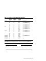
Digital Alpha VME 4 Functional Specifications . . . .
Physical and Environmental Specifications . . . . . . .
Typical Peak Power Supply Current and Module
Power Dissipation . . . . . . . . . . . . . . . . . . . . . . . . . .
Digital Alpha VME 4 Hardware Kit Items . . . . . . . .
Digital Alpha VME 4 Memory Modules . . . . . . . . . .
Digital Alpha VME 4 Cache Memory Modules . . . . .
Additional Hardware Installation Items . . . . . . . . .
Digital Alpha VME 4 Module Configuration
Switches . . . . . . . . . . . . . . . . . . . . . . . . . . . . . . . . . .
Supported Switch Settings for Digital Alpha VME 4
Modules in Slot 1 (System Controller) . . . . . . . . . . .
Supported Switch Settings for Digital Alpha VME
4 Modules in Other Than Slot 1 (Nonsystem
Controller) . . . . . . . . . . . . . . . . . . . . . . . . . . . . . . . .
Digital Alpha VME 4 Memory Configurations . . . . .
J9 Cache Jumper Settings . . . . . . . . . . . . . . . . . . . .
J10 Cache Jumper Settings . . . . . . . . . . . . . . . . . . .
SROM Test Numbers and Descriptions . . . . . . . . . .
Console Code Test Letters and Names . . . . . . . . . . .
Troubleshooting . . . . . . . . . . . . . . . . . . . . . . . . . . . .
Products With a 1 Year Return to Digital Warranty .
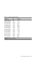
Field Replaceable Units and Order Numbers . . . . . .
.
.
.
.
.
.
.
.
3–1
3–2
4–1
5–1
5–2
5–3
5–4
5–5
5–6
5–7
5–8
6–1
6–2
6–3
6–4
6–5
6–6
6–7
6–8
6–9
6–10
7–1
7–2
7–3
7–4
7–5
7–6
7–7
7–8
7–9
7–10
7–11
7–12
8–1
8–2
9–1
Controls and Indicators . . . . . . . . . . . . . . . . . . . . . . . .
Environment Variable Summary . . . . . . . . . . . . . . . . .
Console Diagnostic Tests . . . . . . . . . . . . . . . . . . . . . . .
System Bus Address Space Description . . . . . . . . . . . .
PCI Sparse I/O Space Byte Enable Generation . . . . . .
PCI Configuration Space Definition . . . . . . . . . . . . . . .
PCI Address Decoding for Primary Bus Configuration
Accesses . . . . . . . . . . . . . . . . . . . . . . . . . . . . . . . . . . . .
PCI Sparse Memory Space Byte Enable Generation . .
PCI Target Window Enables . . . . . . . . . . . . . . . . . . . .
PCI Target Address Translation—Direct Mapped . . . .
Scatter-Gather Map Address . . . . . . . . . . . . . . . . . . . .
CSR Register Addresses for DECchip 21071-CA . . . . .
General Control Register . . . . . . . . . . . . . . . . . . . . . . .
Error and Diagnostic Status Register . . . . . . . . . . . . .
Cache Size Tag Enable Values . . . . . . . . . . . . . . . . . . .
Maximum Memory Tag Enable Values . . . . . . . . . . . . .
Configuration Register for Banks 0 and 1 . . . . . . . . . .
Timing Register A . . . . . . . . . . . . . . . . . . . . . . . . . . . .
Timing Register B . . . . . . . . . . . . . . . . . . . . . . . . . . . .
Global Timing Register . . . . . . . . . . . . . . . . . . . . . . . .
Refresh Timing Register . . . . . . . . . . . . . . . . . . . . . . .
DECchip 21071-DA CSR Addresses . . . . . . . . . . . . . . .
Diagnostic Control/Status Register . . . . . . . . . . . . . . .
PCI Error Address Register . . . . . . . . . . . . . . . . . . . . .
System Bus Error Address Register . . . . . . . . . . . . . . .
Translated Base Registers 1 and 2 . . . . . . . . . . . . . . . .
PCI Base Registers 1 and 2 . . . . . . . . . . . . . . . . . . . . .
PCI Mask Registers 1 and 2 . . . . . . . . . . . . . . . . . . . .
Host Address Extension Register 1 . . . . . . . . . . . . . . .
Host Address Extension Register 2 . . . . . . . . . . . . . . .
PCI Master Latency Timer Register . . . . . . . . . . . . . . .
TLB Tag Registers 0 Through 7 . . . . . . . . . . . . . . . . . .
TLB Data Registers 0 Through 7 . . . . . . . . . . . . . . . . .
Ethernet Controller CSRs . . . . . . . . . . . . . . . . . . . . . .
SCSI Controller CSRs . . . . . . . . . . . . . . . . . . . . . . . . .
PCI Control Register . . . . . . . . . . . . . . . . . . . . . . . . . .
3–2
3–4
4–3
5–3
5–7
5–8
5–9
5–13
5–16
5–18
5–20
6–9
6–12
6–14
6–17
6–18
6–23
6–25
6–27
6–28
6–29
7–7
7–10
7–14
7–15
7–16
7–16
7–18
7–19
7–19
7–20
7–21
7–22
8–5
8–9
9–3
xvii
9–2
9–3
9–4
9–5
9–6
9–7
9–8
9–9
9–10
9–11
9–12
9–13
9–14
9–15
9–16
9–17
9–18
9–19
10–1
10–2
10–3
10–4
10–5
10–6
10–7
10–8
10–9
10–10
10–11
10–12
10–13
10–14
10–15
10–16
xviii
Module Configuration Register . . . . . . . . . . . . . . . . . . .
DIMM Identification . . . . . . . . . . . . . . . . . . . . . . . . . .
Presence Detect . . . . . . . . . . . . . . . . . . . . . . . . . . . . . .
ID Bits . . . . . . . . . . . . . . . . . . . . . . . . . . . . . . . . . . . . .
Memory DIMM Configuration Bit . . . . . . . . . . . . . . . .
Reset Reason Registers . . . . . . . . . . . . . . . . . . . . . . . .
Module Control Register . . . . . . . . . . . . . . . . . . . . . . .
Bcache Size and Speed Decode . . . . . . . . . . . . . . . . . . .
Super I/O Register Address Space Map . . . . . . . . . . . .
Integrated Device Electronics Register Addresses . . . .
Keyboard and Mouse Controller Addresses . . . . . . . . .
TOY Clock Timekeeping Registers . . . . . . . . . . . . . . . .
TOY Clock Command Register . . . . . . . . . . . . . . . . . . .
Timer Interface Registers . . . . . . . . . . . . . . . . . . . . . . .
Interval Timing Control Register . . . . . . . . . . . . . . . . .
Timer Modes . . . . . . . . . . . . . . . . . . . . . . . . . . . . . . . .
Timer Interrupt Status Register . . . . . . . . . . . . . . . . .
Watchdog Timer TOY Clock Command Register . . . . .
Formation of Address Modifier Codes from
Scatter-Gather Entry . . . . . . . . . . . . . . . . . . . . . . . . . .
VIC Block Transfer Control Register . . . . . . . . . . . . . .
VME Address . . . . . . . . . . . . . . . . . . . . . . . . . . . . . . . .
PCI Address . . . . . . . . . . . . . . . . . . . . . . . . . . . . . . . . .
VME Interface Processor Page Monitor CSR . . . . . . . .
Interprocessor Communication Register Map Through
VIF_ABR . . . . . . . . . . . . . . . . . . . . . . . . . . . . . . . . . . .
Arbiter/Requester Configuration Register . . . . . . . . . .
VIC Release Control Register . . . . . . . . . . . . . . . . . . . .
VMEbus Transfer Timeout Register . . . . . . . . . . . . . . .
VIC Interrupt Request/Status Register . . . . . . . . . . . .
VMEbus Interrupter Interrupt Control Register . . . . .
Swap Modes . . . . . . . . . . . . . . . . . . . . . . . . . . . . . . . . .
PCI BE# to Local A1,0 and SIZ1,0 Translation for
Various Swap Modes . . . . . . . . . . . . . . . . . . . . . . . . . .
Local Bus A1,0 and SIZ1,0 to PCI BE# Translation . . .
Access to PCI Memory Addresses . . . . . . . . . . . . . . . . .
VME_IF_BASE + . . . . . . . . . . . . . . . . . . . . . . . . . . . . .
9–7
9–9
9–11
9–12
9–12
9–13
9–15
9–17
9–19
9–21
9–22
9–23
9–24
9–26
9–27
9–29
9–32
9–35
10–6
10–8
10–12
10–13
10–14
10–15
10–19
10–20
10–22
10–24
10–25
10–26
10–29
10–30
10–31
10–37
11–1
11–2
11–3
11–4
12–1
12–2
12–3
A–1
A–2
A–3
A–4
A–5
A–6
A–7
A–8
Table of CPU Interrupt Assignments . . . . . . . . . . . .
VIC64 Chip Interrupt Ranking . . . . . . . . . . . . . . . .
VME IRQ ICR Priority Assignments . . . . . . . . . . . .
NMI Status and Control Register Bits . . . . . . . . . . .
Commonly Used Commands . . . . . . . . . . . . . . . . . . .
Console Shell Operators . . . . . . . . . . . . . . . . . . . . .
Digital Alpha VME 4 Console Command Summary
.........................................
VMEbus (J1) Connector . . . . . . . . . . . . . . . . . . . . . .
Console (J6) and Serial (J7) Connector Pinouts . . . .
Ethernet (J9) Connector Pinouts . . . . . . . . . . . . . . .
Primary Breakout Module Connector Pinouts . . . . .
Keyboard and Mouse (J1) Connector . . . . . . . . . . . .
Parallel Port (J6) Connector . . . . . . . . . . . . . . . . . . .
PMC I/O Companion Card Mouse (J2) Connector . .
PMC I/O Companion Card Keyboard (J3)
Connector . . . . . . . . . . . . . . . . . . . . . . . . . . . . . . . . .
.
.
.
.
.
.
.
.
.
.
.
.
11–1
11–6
11–8
11–12
12–2
12–3
.
.
.
.
.
.
.
.
.
.
.
.
.
.
.
.
12–18
A–2
A–3
A–4
A–4
A–8
A–8
A–10
..
A–10
xix
Preface
Purpose of this Manual
This manual describes the Digital Alpha VME 4 module. It provides configuration
and installation procedures and describes the module’s built-in features, including
the console code and diagnostics.
Intended Audience
This manual is for OEM system integrators who have extensive knowledge of
single-board computers (SBCs). Their task is to integrate Digital Alpha VME 4
modules into their own systems. The system integrators need information about
the Digital Alpha VME 4 module’s physical and environmental specifications
and performance. They also need information, such as register descriptions, to
program the module.
A secondary audience consists of manufacturing technicians who install the
module and field technicians who diagnose problems and replace modules.
This manual does not explain how to use specific operating system programming
interfaces. For this information, see the appropriate operating system
documentation.
Structure of this Manual
This manual consists of 13 chapters, an appendix, and an index.
•
Chapter 1, Product Overview, provides a general product description, lists
product features and functional specifications, and identifies physical and
environmental requirements.
•
Chapter 2, Installation Procedures, explains how to unpack and install the
Digital Alpha VME 4 module. This chapter also introduces diagnostics and
troubleshooting and provides repair and warranty information.
xxi
•
Chapter 3, Operating the Digital Alpha VME 4 Computer, explains how to
use the Digital Alpha VME 4 module’s controls and indicators, introduces
console mode and environment variables, and provides pointers to information
on booting operating systems and updating firmware.
•
Chapter 4, Diagnostics, describes the Digital Alpha VME 4 power-on self-test
(POST) diagnostics and ROM based diagnostics (RBDs).
•
Chapter 5, System Address Mapping, describes the mapping of 34-bit
processor physical address space to memory and I/O space addresses. This
chapter also includes discussions on address translations.
•
Chapter 6, Cache and Memory Subsystem, describes the cache and memory
subsystem. This chapter includes discussions on error handling and describes
the subsystem’s address space and registers.
•
Chapter 7, PCI Host Bridge, describes the PCI host bridge that resides
between the PCI local bus and the system bus. This chapter discusses the
interfaces to the system bus and PCI bus and describes the related address
space and registers.
•
Chapter 8, PCI bus, describes the PCI bus, the base of the I/O subsystem.
The chapter describes the various I/O devices and their registers.
•
Chapter 9, Nbus, decribes the Digital Alpha VME 4 module’s Nbus. The
discussion includes the Nbus address space and registers. This chapter also
includes information on ROM, the Super I/O chip, the keyboard and mouse
controller, the time-of-year (TOY) clock, interval timer registers, the watchdog
timer, and nonvolatile RAM (NVRAM).
•
Chapter 10, VME Interface, describes the interface that handles the VMEbus
and its interacations with the PCI bus. The chapter describes master and
slave address spaces, address mapping, registers, and communication. The
chapter also discusses system controller operation, byte swapping addressing,
and interface initialization.
•
Chapter 11, System Interrupts, describes Digital Alpha VME 4 system
interrupts and how the module can be reset.
•
Chapter 12, Console Primer, introduces you to the Digital Alpha VME 4
console and explains how to use basic console commands.
•
Chapter 13, Console Commands, describes the Digital Alpha VME 4 console
commands.
•
Appendix A, Module Connector Pinouts, provides pinout information for the
Digital Alpha VME 4 module connectors.
xxii
Conventions
This section defines terminology, abbreviations, and other conventions used in
this manual.
Abbreviations
•
Register access
The following list describes the register bit and field abbreviations:
•
Bit/Field Abbreviation
Description
MBZ (must be zero)
Bits and fields specified as MBZ must be zero.
RO (read only)
Bits and fields specified as RO can be read but not
written.
RW (read/write)
Bits and fields specified as RW can be read and
written.
WO (write only)
Bits and fields specified as WO can be written but not
read.
Binary multiples
The abbreviations K, M, and G (kilo, mega, and giga) represent binary
multiples and have the following values:
K
= 210 (1024)
M
= 220 (1,048,576)
G
= 230 (1,073,741,824)
For example:
2 KB
= 2 kilobytes
4 MB
= 4 megabytes
8 GB
= 8 gigabytes
= 2 3 210 bytes
= 4 3 220 bytes
= 8 3 230 bytes
Addresses
Unless otherwise noted, addresses and offsets are hexadecimal values.
Bit Notation
Multiple-bit fields can include contiguous and noncontiguous bits contained in
angle brackets ( <> ). Multiple contiguous bits are indicated by a pair of numbers
separated by a colon ( : ). For example, <9:7,5,2:0> specifies bits 9, 8, 7, 5, 2, 1,
and 0. Similarly, single bits are frequently indicated with angle brackets. For
example, <27> specifies bit 27.
xxiii
Caution
Cautions indicate potential damage to equipment or loss of data.
Data Field Size
The term INTnn, where nn is one of 2, 4, 8, 16, 32, or 64, refers to a data field
of nn contiguous NATURALLY ALIGNED bytes. For example, INT4 refers to a
NATURALLY ALIGNED longword.
Data Units
The following data unit terminology is used throughout this manual.
Term
Words
Bytes
Bits
Other
Byte
1/2
1
8
—
Word
1
2
16
—
Longword/Dword
2
4
32
Longword
Quadword
4
8
64
2 Longwords
Octaword
8
16
128
2 Quadwords
Hexword
16
32
256
2 Octawords
Examples
The prompts, input, and output in examples are shown in a monospaced font.
Interactive input is differentiated from prompts and system output with bold
type. For example:
>>> echo This is a test.
This is a test.
Ellipsis points indicate that a portion of an example is omitted.
Keyboard Keys
The following keyboard key conventions are used throughout this manual.
Convention
Example
Control key sequences are represented as Ctrl/x. Press
Ctrl while you simultaneously press the x key.
Ctrl/C
In plain text, key names match the name on the actual
key.
Return key
In tables, key names match the name of the actual key
and appear in a box.
xxiv
Return
Names and Symbols
The following table lists typographical conventions used for names of various
items throughout this manual.
Items
Example
Bits
sysBus<32:2>
Commands
boot command
Command arguments
address argument
Command options
-sb option
Environment variables
AUTO_ACTION
Environment variable values
HALT
Files and pathnames
/usr/foo/bar
Pins
LIRQ pin
Register symbols
VIP_ICR register
Signals
iogrant signal
Variables
n, x, mydev
Note
Notes emphasize particularly important information.
Numbering
Numbers are decimal or hexadecimal unless otherwise indicated. The prefix
0x indicates a hexadecimal number. For example, 19 is decimal, but 0x19 and
0x19A are hexadecimal (see also Addresses). Otherwise, the base is indicated by
a subscript; for example, 1002 is a binary number.
Ranges and Extents
Ranges are specified by a pair of numbers separated by two periods ( .. ) and are
inclusive. For example, a range of integers 0..4 includes the integers 0, 1, 2, 3,
and 4.
Extents are specified by a pair of numbers in angle brackets ( <> ) separated by a
colon ( : ) and are inclusive. Bit fields are often specified as extents. For example,
bits <7:3> specifies bits 7, 6, 5, 4, and 3.
Register and Memory Figures
Register figures have bit and field position numbering starting at the right
(low-order) and increasing to the left (high-order).
Memory figures have addresses starting at the top and increasing toward the
bottom.
xxv
Syntax
The following syntax elements are used throughout this manual. Do not type the
syntax elements when entering information.
Element
Example
Description
[]
[-file filename]
The enclosed items are optional.
|
- | + | =
Choose one of two or more items. Select
one of the items unless the items are
optional.
{}
{- | + | =}
You must specify one (and only one) of the
enclosed items.
()
—
You must specify the enclosed items
together.
arg . . .
You can repeat the preceding item one or
more times.
...
UNPREDICTABLE and UNDEFINED
In this manual, the terms UNPREDICTABLE and UNDEFINED are used. Their
meanings are different and must be carefully distinguished.
In particular, only privileged software (that is, software running in kernel mode)
can trigger UNDEFINED operations. Unprivileged software cannot trigger
UNDEFINED operations. However, either privileged or unprivileged software can
trigger UNPREDICTABLE results or occurrences.
UNPREDICTABLE results or occurrences do not disrupt the basic operation
of the processor. The processor continues to execute instructions in its normal
manner. In contrast, UNDEFINED operations can halt the processor or cause it
to lose information.
The terms UNPREDICTABLE and UNDEFINED can be further described as
follows:
•
UNPREDICTABLE
Results or occurrences specified as UNPREDICTABLE might vary from
moment to moment, implementation to implementation, and instruction
to instruction within implementations. Software can never depend on
results specified as UNPREDICTABLE.
An UNPREDICTABLE result might acquire an arbitrary value subject
to a few constraints. Such a result might be an arbitrary function of the
input operands or of any state information that is accessible to the process
in its current access mode. UNPREDICTABLE results may be unchanged
from their previous values.
xxvi
Operations that produce UNPREDICTABLE results might also produce
exceptions.
An occurrence specifed as UNPREDICTABLE might happen or not based
on an arbitrary choice function. The choice function is subject to the same
constraints as are UNPREDICTABLE results and, in particular, must not
constitute a security hole.
Specifically, UNPREDICTABLE results must not depend upon, or be
a function of the contents of memory locations or registers that are
inaccessible to the current process in the current access mode.
Also, operations that might produce UNPREDICTABLE results must not
write or modify the contents of memory locations or registers to which the
current process in the current access mode does not have access. They
must also not halt or hang the system or any of its components.
For example, a security hole would exist if some UNPREDICTABLE
result depended on the value of a register in another process, on the
contents of processor temporary registers left behind by some previously
running process, or on a sequence of actions of different processes.
•
UNDEFINED
Operations specified as UNDEFINED can vary from moment to moment,
implementation to implementation, and instruction to instruction within
implementations. The operation can vary in effect from nothing, to
stopping system operation.
UNDEFINED operations can halt the processor or cause it to lose
information. However, UNDEFINED operations must not cause the
processor to hang, that is, reach an unhalted state from which there is no
transition to a normal state in which the machine executes instructions.
Only privileged software (that is, software running in kernel mode) can
trigger UNDEFINED operations.
xxvii
For More Information
Document
Order Number
CY7C9640 Specification
Company
Cypress
Semiconductor
Corp.
DECchip 21040–AA Specification
EC–N0752–72
Digital Equipment
Corp.
DECchip 21064–AA Microprocessor Hardware
Reference Manual
EC–N0079–72
Digital Equipment
Corp.
DECchip 21072–AA Core Logic Chip Set
EC–N0648–72
Digital Equipment
Corp.
Digital UNIX Installation Guide
AA–PS2DD–TE
Digital Equipment
Corp.
Intel SIO82378 Chip Specification
Intel Corp.
Internetworking with TCP/IP, Vol I,
Principles, Protocols and Architecture, Second
edition, Prentice Hall.
PCI Local Bus Specification
Intel Corp.
NCR 53C810 Specification
National Cash
Register Co.
NCR 53C720 Programming Guide
National Cash
Register Co.
SIO Chip (82378ZB) and 8259 Data Sheets
Intel Corp.
VIC64 Specification
Cypress
Semiconductor
Corp.
VxWorks Digital AXPvme Single-Board
Computers Hardware Supplement
AA-QA5HA-TE
Digital Equipment
Corp.
VxWorks Programmer’s Guide
AA–Q3YLB–TE
Digital Equipment
Corp.
xxviii
1
Product Overview
1.1 Product Description
The Digital Alpha VME 4/224 and 4/288 MHz single-board computers are based
on the 21064A Alpha processor chip. The Digital Alpha VME 4/224 comes
preconfigured with 512 KB cache, and the Digital Alpha VME 4/288 comes
preconfigured with 2 MB cache.
The board utilizes the Peripheral Component Interconnect (PCI) as the on-board
bus for the interconnection of high performance SCSI, Ethernet, and VME
interfaces, as well as the connection of industry-standard PCI mezzanine cards
(PMCs—IEEE P1386.1 standard).
The Digital Alpha VME 4 processors are supported by the VxWorks for Alpha and
Digital UNIX operating systems.
1.2 Functional Specifications
Table 1–1 lists the Digital Alpha VME 4 processor functional specifications.
Figure 1–1 is a block diagram of the Digital Alpha VME 4 processor.
Product Overview 1–1
Table 1–1 Digital Alpha VME 4 Functional Specifications
Item
Description
Alpha AXP processor
21064A Alpha processor with on-chip 16 KB instruction and 16
KB data caches IEEE and VAX floating point.
Peformance
At 288 MHz, 238.51 SPECfp92, 188.84 SPECint92, 5.44
SPECfp95, and 4.69 SPECint95.
Network features
DECchip 21040 PCI Ethernet controller DMA (bus master),
256 byte send and receive FIFO, double bandwidth with full
duplex Ethernet (PCI based).
Network Interconnect
10BASE-T Ethernet (twisted pair).
Memory
Cache - 512 KB or 2 MB using cache modules.
Main memory ECC protected 8, 16, 32, 64, and 128 MB using
memory DIMMS on 128-bit data bus with single-bit error
detection. Accessible from the CPU, PCI, and VMEbus.
4 MB flash EPROM.
32 KB NVRAM.
SCSI-2
NCR 53C810 PCI based SCSI-2 processor single-ended 8-bit
with DMA, up to 10 MB transfer rate with connection through
the VMEbus P2 connector.
Serial and parallel
interfaces
Two asynchronous DEC423 ports, 75 to 19200 baud through
front panel MMJ connectors.
Keyboard and mouse support for graphics options on either the
secondary breakout module or the PMC I/O companion card.
Extended parallel port through the secondary breakout module.
Clocks and timers
Real-time clock with battery backup.
Three 16-bit timers.
Watchdog timer with programmable reset.
VMEbus
High performance PCI to VME64 interface chip capable of
DMA transfers, implemented with the VIC64 interface chip.
PCI expansion
Accepts one double-width or two single-width PCI mezzanine
card (PMC) modules with optional I/O companion card.
Physical
6U VME form factor requiring two adjacent slots. Three
adjacent slots are required with the optional PMC I/O
companion card.
1–2 Product Overview
Figure 1–1 Digital Alpha VME 4 Block Diagram
Cache and
Memory
Controller
CPU
128
memdata
64
Bcache
CPU Board
Data Path
4 chips
sysBus 128 Bits
PCI Host
Bridge
(21071-DA)
Main
Memory
32
epiData
(DS1386)
I/O Board
TOY Clock
Interrupt
Controller
PCI to
Nbus
Bridge
Flash
Watchdog Timer
NVRAM
Nbus 8 Bits
Keyboard
and Mouse
Controller
Super
I/O
Interval
Timer
PCI Bus 32 Bits
PCI-VME
Bridge
SCSI
Controller
Ethernet
Controller
PCI to
PCI Bridge
PCI/PMC
option 0 slot
VME Connectors
PCI/PMC
option 1 slot
PMC Expander Card
ML013270
Product Overview 1–3
1.3 Physical and Environmental Requirements
The Digital Alpha VME 4 module requires a VME chassis with sufficient cooling.
You must have at least 200 linear feet/minute (lfm) of airflow at an ambient
temperature of not more than 40°C (104°F) across the processor heatsink.
Table 1–2 shows the physical and environmental specifications for the Digital
Alpha VME 4 module. Table 1–3 shows the power supply current and power
dissipation for the Digital Alpha VME 4 module. Stresses beyond those specified
may cause permanent damage to the module.
Table 1–2 Physical and Environmental Specifications
Characteristic
Specification
Industry standard
VME 6U module
Operating temperature
0°C to 40°C (32°F to 104°F)
Storage temperature
–40°C to 66°C (–40°F to 151°F)
Temperature change
20°C/hour (36°F/hour)
Relative humidity
5% to 95% (noncondensing)
Airflow
200 lfm minimum at 40°C ambient inlet air temperature,
over the large square processor heatsink and cache
Vibration:
Operating in a suitable enclosure
0.5 g Pk 22.1–260 Hz
0.25 g Pk 200–500 Hz
1–4 Product Overview
Table 1–3 Typical Peak Power Supply Current and Module Power Dissipation
CPU Modules
w/128 MB Memory
Amps
@5V
Amps @ 12 V
(note 1)
Amps
@012 V
Module Heat
Dissipation
Alpha VME 4/224
12.0 A
0.2 A
0.01 A
62 W
Alpha VME 4/288
13.5 A
0.2 A
0.01 A
70 W
Options
Amps
@5V
Amps
@ 12 V
Amps
@012 V
Power
Dissipation
SCSI Termination
0.8 A max.
0.0 A
N/A
4 W max.
PMC Option Slot
Budget
3.0 A max.
N/A
N/A
15 W max.
Notes
Power and heat dissipation assumes nominal voltages (5.0 V, 12.0 V, and
012 V). Power numbers are based on actual measured data. Add 10% to
the current and power values for a worst-case power and heat scenario.
SCSI Termination is enabled by default. You can disable this option by
resetting the jumper on the primary breakout module as explained in
Section 8.2.1.
For more information about the PMC option slot budget, see the
documentation supplied with your PMC option.
Product Overview 1–5
2
Installation Procedures
This chapter describes how to unpack, configure, install, and verify proper
operation of the Digital Alpha VME 4 module.
2.1 Unpacking
Your Digital Alpha VME 4 hardware kit contains the items listed in Table 2–1.
Save the original packing material in case a factory return is necessary.
Caution
You must install the primary breakout module (54-24663-01) included
in your hardware kit (see Figure 2–7). Applying power to the Digital
Alpha VME 4 module WITHOUT that primary breakout module in place,
or WITH the breakout module included with the AXPvme 160, 166, or
230 (P/N 54–22605–01) in place may damage your backplane, the Digital
Alpha VME 4 module, or both.
Figure 2–1 shows the Digital Alpha VME 4 module and its options.
Installation Procedures 2–1
Figure 2–1 Digital Alpha VME 4 Module Components
1
2
3
4
7
5
!
"
#
$
%
&
'
6
MLO-013240
Optional PMC I/O companion card
I/O module
Digital Alpha VME 4 module
Memory modules
Cache memory modules
Secondary breakout module
Primary breakout module
Table 2–1 lists Digital Alpha VME 4 hardware kit items. The kits in Table 2–1
contain hardware only. The option you receive may also include software licenses
or software, depending on what is ordered.
2–2 Installation Procedures
Table 2–1 Digital Alpha VME 4 Hardware Kit Items
Item
Part Number
Digital Alpha VME 4/224 Kit
Digital Alpha VME 4 module I/O assembly
Digital Alpha VME 4 Primary breakout module
70–32976–04 (includes 512 KB cache)
(54–24325–04 + 54–24319–01)
1
54–24663–01
Digital Alpha VME 4 Secondary breakout module
54–24729–01
Alpha VME 4/228 and 4/288 Single-Board
Computers User’s Guide and Technical
Description
EK–DAVME–TD
Antistatic wriststrap
12–36175–01
Digital Alpha VME 4/288 Kit
Digital Alpha VME 4 module I/O assembly
Digital Alpha VME 4 Primary breakout module
70-32976-02 (includes 2 MB cache)
(54–24325–02 + 54–24319–01)
1
54–24663–01
Digital Alpha VME 4 Secondary breakout module
54–24729–01
Alpha VME 4/228 and 4/288 Single-Board
Computers User Guide and Technical Description
EK–DAVME–TD
Antistatic wriststrap
12–36175–01
Optional PMC I/O Companion Card
PMC I/O Companion Card
54–24665–01
Y cable
17-04230-01
1
Installation necessary for operation of VME 4 module I/O assembly.
To install the Digital Alpha VME 4 module, you must also have one or more of the
memory and cache module sets listed in Tables 2–2 and 2–3. Each kit contains
two modules.
Installation Procedures 2–3
Table 2–2 Digital Alpha VME 4 Memory Modules
Memory Size
(MB)
Kit Number
Part Number
16
EBMXM-DB
54–24659–AB
32
EBMXM-EB
54–24659–AA
64
EBMXM-FB
54–24645–AA
Table 2–3 Digital Alpha VME 4 Cache Memory Modules
Memory Size
Kit Number
Part Number
Quantity
512 KB
EBMXC–BA
54–24685–AA
2
2 MB
EBMXC–DB
54–24683–AA
2
Depending on how you plan to use the Digital Alpha VME 4 system, you may
need one or more of the items listed in Table 2–4 that are not part of the Digital
Alpha VME 4 kit.
In order to attach a local disk, a 50-pin IDC SCSI cable is required and must be
properly terminated. The exact cable requirements depend upon the enclosure,
disk mounting, and so forth. A PC ‘‘internal SCSI cable’’ will work if you are
connecting to an internal disk and the cable has a SCSI terminator, or if the last
disk (or other SCSI device) has an internal terminator. You can use the Digital
SCSI cables listed in Table 2–4 for this purpose.
To attach a printer to the parallel port of the secondary breakout module (5424729-01), use any standard parallel port printer cable that has a 26 pin IDC
connector on one end (for example, 17-04060-01). When you connect the cable,
make sure pin 1 of the cable is on pin 1 of the connector that is mounted on the
breakout module.
2–4 Installation Procedures
Table 2–4 Additional Hardware Installation Items
Item
Supplier
Part Number
Serial line cable for console and auxiliary
terminals
Digital
BC16E– nn1
IEEE 802.3 Twisted-pair transceiver to ThinWire
Digital
DETTR–AA
IEEE 802.3 Twisted-pair transceiver to twistedpair
Digital
DETTR–BB
10BASET loopback connector
Digital
12-35619-01
(H4082-AA)
SCSI 20.32 cm (8 in), 30.48 cm (12 in), or 53.34
cm (21 in) cable with a 50-pin female IDC
connector for connection to the Alpha VME
breakout module and a female IEEE (Champ)
connector for connection to external drives2
Digital
17-01244-01, -02, -03
SCSI 102.87 cm (40.5 in) cable with six 50-pin
female IDC connectors and an included 50-pin
IDC SCSI terminator for connection to the Alpha
VME breakout module and up to 4 internal drives
with the terminator on the last connector
Digital
17–03459–02
SCSI 220.98 cm (87 in) cable with five 50-pin
female IDC connectors for connection to the
Alpha VME breakout module and up to 4 internal
drives and a female IEEE (Champ) connector for
connection to external drives2
Digital
17-03036-01
Parallel port cable (example)
Digital
17-04060-01
1
The nn = cable length.
2
A Champ SCSI terminator (PN H8574-A) might be required if external drives are not connected.
Installation Procedures 2–5
2.2 Installation
To install the Digital Alpha VME 4 module, perform the following steps:
1. Select two adjacent slots in your VME backplane for the Digital Alpha VME
4 module. If you are installing a PMC I/O companion card, you will need to
select three adjacent slots. Refer to Section 2.2.1 for instructions on how to
install the PMC I/O companion card.
Caution
Static electricity can destroy the circuits on the modules in your Digital
Alpha VME 4 kit. When you handle modules wear the antistatic
wriststrap with the wire clipped to the frame of your VME chassis. Also,
place the modules on top of the conductive plastic bags they came in while
you work.
Note
There must be sufficient space on the back of the VME backplane slot or
slots selected to install the primary breakout module. The Digital Alpha
VME 4 primary breakout module requires a minimum of 38.1 mm (1.5
in).
Figure 2–2 and Figure 2–3 show the layout of Digital Alpha VME 4 and the
I/O modules.
2–6 Installation Procedures
Figure 2–2 Digital Alpha VME 4 Module Layout
8
9
7
1
2 MB
C
B
A
2
6
512 KB
5
4
3
512 KB
C
B
A
D
C
B
A
2 MB
D
C
B
A
MLO-013237
!
"
#
$
%
&
'
(
)
Cache memory connectors
Memory connectors
Cache configuration select jumper (J9)
Power and VME slave activity/watchdog timeout LEDs
Status display
Cache memory size and speed select jumper (J10)
I/O module connector
VME connectors
SROM (8 pin)
Installation Procedures 2–7
Figure 2–3 I/O Module Layout
5
6
7
OPEN
OFF
4
9
3
2
1
ON
8
10
4
!
"
#
$
%
&
'
(
)
+>
3
1
2
MLO-013238
Console serial port
Auxiliary serial port
Reset/halt switch
Twisted pair Ethernet connector
Connector to CPU module (on back of I/O module)
Debug jumper (not installed for normal operation)
Configuration switchpack
PMC I/O companion card connector
Ethernet Address ROM
NVRAM/TOY clock
2–8 Installation Procedures
2. Set the configuration switches on the I/O module as outlined in Table 2–5,
Table 2–6, and Table 2–7. Also refer to Figure 2–3 for the configuration
switch location.
Table 2–5 Digital Alpha VME 4 Module Configuration Switches
Switch
Setting
Function
1
Closed
Supplies +5 V from the VMEbus +5 V Standby signal to the timeof-year (TOY) clock and the nonvolatile random-access memory
(NVRAM) to supplement the internal battery when the Digital
Alpha VME 4 module is turned off.
Open
Does not supply power from the VMEbus +5 V Standby signal. The
internal battery will last for about 10 years with the Digital Alpha
VME 4 module power turned off.
Closed
Enables writing of flash ROMs under program control.
Open
Disables writing of flash ROMs.
Closed
Resets the Digital Alpha VME 4 module on VMEbus Reset signal.
Open
Does not reset the Digital Alpha VME 4 module on VMEbus Reset
signal.
Closed
Digital Alpha VME 4 module is VMEbus system controller.
Open
Digital Alpha VME 4 module is not VMEbus system controller.
2
3
4
Table 2–6 Supported Switch Settings for Digital Alpha VME 4 Modules in Slot 1
(System Controller)
Switch
Setting
1
Closed
2
Open
3
Open1
4
Closed1
1
These switches are required to be in the indicated positions for reliable system operation during a
VMEbus Reset.
Installation Procedures 2–9
Table 2–7 Supported Switch Settings for Digital Alpha VME 4 Modules in Other
Than Slot 1 (Nonsystem Controller)
Switch
Setting
1
Closed
2
Open
3
Closed1
4
Open1
1
These switches are required to be in the indicated positions (one opened, one closed) for reliable
system operation during a VMEbus Reset.
3. Install the memory module on your Digital Alpha VME 4 module (Figure 2–4)
in the following manner:
•
Populate bank 0 first, then bank 1, if necessary.
•
Memory installed in a bank must be the same size and speed.
•
Align pin 1 of the memory module with pin 1 on the connector. The
position of the orientation notches (see
in Figure 2–4) assure proper
connectivity.
2–10 Installation Procedures
#
Figure 2–4 Installing the Main Memory Modules
1
2
4
3
MLO-013246
!
"
#
$
Memory bank 0 slots A and B
Memory bank 1 slots A and B
Orientation notches
Memory connector
Table 2–8 shows all possible valid memory configurations.
Installation Procedures 2–11
Table 2–8 Digital Alpha VME 4 Memory Configurations
Memory Size
(MB)
Bank 0
Slot A
Bank 0
Slot B
Bank 1
Slot A
Bank 1
Slot B
16
8
8
32
8
8
32
16
16
8
8
48
8
8
16
16
64
16
16
16
16
64
32
32
96
16
16
32
32
96
32
32
16
16
128
32
32
32
32
4. Cache memory DIMMs are installed on your Digital Alpha VME 4 module by
Digital. Pin 1 of the DIMM is aligned with pin 1 on the cache connector. The
position of the orientation notch on the cache memory DIMM in Figure 2–5
(see ) denotes the location of pin 1.
!
2–12 Installation Procedures
Figure 2–5 Cache Memory Modules
1
2
MLO-013245
!
"
Orientation notch
Cache memory connector
5. The J9 and J10 jumpers are preconfigured for your Digital Alpha VME 4
module by Digital. Table 2–9, Table 2–10, and Figure 2–2 show jumper
settings and locations for informational purposes only.
Table 2–9 J9 Cache Jumper Settings
Size
A
B
C
D
512 KB
Out
Out
In
In
2 MB
Out
Out
In
In
Installation Procedures 2–13
Table 2–10 J10 Cache Jumper Settings
A
B
C
Total Size
In
In
In
Disable cache
In
In
Out
Reserved
In
Out
In
2 MB
In
Out
Out
Reserved
Out
In
In
512 KB
Out
In
Out
Reserved
Out
Out
In
Reserved
Out
Out
Out
Reserved
Speed
12 ns
15 ns
Note
If you are installing the PMC I/O companion card, proceed to Section 2.2.1
later in this chapter and complete the installation instructions before
continuing on to step 6.
6. Install the Digital Alpha VME 4 module into the VME chassis (refer to
Figure 2–6). Note that the module requires two adjacent backplane slots.
Secure the module with screws as shown in callout .
!
2–14 Installation Procedures
Figure 2–6 Installing the Digital Alpha VME 4 Module
1
MLO-013236
Caution
You must install the primary breakout module (54-24663-01) included
in your hardware kit (see Figure 2–7). Applying power to the Digital
Alpha VME 4 module WITHOUT that primary breakout module in place,
or WITH the breakout module included with the AXPvme 160, 166, or
230 (P/N 54–22605–01) in place may damage your backplane, the Digital
Alpha VME 4 module, or both. Also, do not press on the LED window
when you install the module.
Installation Procedures 2–15
2
4
6
3
5
!
1
Figure 2–7 Alpha VME 4 Primary Breakout Module
Part Number: 54-24663-01
Part Number: 54-22605-01
MLO-013263
7. Set the SCSI termination jumper on the breakout module (refer to
Figure 2–8).
The SCSI bus must be terminated at each end. In most installations, the
breakout module is one end of the SCSI bus and the far end of the SCSI
ribbon cable is the other end of the SCSI bus. In this case, enable the SCSI
termination by placing the jumper across pins 1 and 3 (default).
If the breakout module is not at the end of the SCSI bus, disable the SCSI
termination by placing the jumper across pins 3 and 5.
8. Set the watchdog signal jumper on the breakout module (refer to Figure 2–8).
The Digital Alpha VME 4 module supplies an external watchdog reset signal
that you can connect to a monitoring device. If you make no connection to
this external signal, the setting of the jumper makes no difference.
Setting the jumper across pins 4 and 6 (default) provides an internal 2 kOhm
to +5 V pullup for this signal. Setting the jumper across pins 2 and 4 provides
no pullup. This allows you to attach a monitoring device that operates at a
different voltage level. The monitoring device must provide voltage and
a pullup resistor that do not exceed the output specifications of a 74LS05
2–16 Installation Procedures
component. The monitoring device must also be connected to the same
ground reference as the Digital Alpha VME 4 module.
The external watchdog reset signal is on pin C10 of the VMEbus J3 (P2)
connector on the breakout module. This signal is low during normal operation
and high during a watchdog timer reset (provided that pullup power is
connected).
Figure 2–8 Primary Breakout Module Jumpers
SCSI Termination
Enabled
5 3 1
6 4 2
Watchdog Pullup
SCSI Termination
Disabled
5 3 1
6 4 2
Watchdog No Pullup
MLO-013261
9. If your Digital Alpha VME 4 system has SCSI devices, connect the SCSI cable
to the primary breakout module (refer to Figure 2–9).
Installation Procedures 2–17
Figure 2–9 Connecting the SCSI Cable to the Primary Breakout Module
MLO-013241
10. Install the primary breakout module (refer to Figure 2–10). Ensure that the
breakout module is installed behind the slots occupied by the Digital Alpha
VME 4 module (as shown).
Caution
Running the Digital Alpha VME 4 module when it is not in the same slots
as the correct breakout module (refer to Figure 2–10) may damage your
backplane, the Digital Alpha VME 4 module, or both.
Never insert a module other than an Digital Alpha VME 4 module into a
slot opposite the breakout module. The breakout module feeds power to
several of the user-defined pins on the P2 backplane connector. This may
damage another VME module.
It is recommended that the slot number and type of breakout module be
recorded to ensure that the Digital Alpha VME 4 modules are always
installed into a slot with the appropriate breakout module.
2–18 Installation Procedures
Figure 2–10 Installing the Primary Breakout Module
MLO-013264
11. A secondary breakout module is included in the hardware kit, which you can
connect to the primary breakout module. If you use the secondary breakout
module, set the jumpers on that module as shown in Figure 2–11.
Note
An incremental clearance of at least 56.25 mm (2.25 inches) is required to
install the secondary breakout module.
Installation Procedures 2–19
Figure 2–11 Secondary Breakout Module Jumpers
Keyboard / Mouse
Disabled
3
Keyboard / Mouse
Enabled
3 1
3 1
3 1
3 1
4 2
4 2
4 2
4 2
2
1
4
MLO-013353
!
"
#
$
Mouse and keyboard connector
Mouse and keyboard Y cable (17-04230-01)
Keyboard and mouse jumper configurations
Parallel port (see Appendix A for pinouts)
12. Connect the secondary breakout module to the primary breakout module as
shown in Figure 2–12.
2–20 Installation Procedures
Figure 2–12 Connecting the Secondary Breakout Module to the Primary
Breakout Module
1
2
MLO-013266
!
"
Primary breakout module (54-24663-01)
Secondary breakout module (54-24729-01)
13. Connect the network cable (if any) to the twisted-pair Ethernet connector. See
Figure 2–13. Associated with the Ethernet connector are devices to convert
from twisted pair to ThinWire (P/N DETTR–AA). See Table 2–4.
14. Connect the console terminal cable to the Digital Alpha VME 4 module (refer
to Figure 2–13).
15. If you have an auxiliary terminal, connect it now. Set your console terminal
to a speed of 9600 bits/second, an 8-bit data word, and no parity.
Installation Procedures 2–21
Figure 2–13 Connecting Network and Console Terminal Cables
1
2
3
MLO-013352
!
"
#
Network
Console
Auxiliary
16. Insert blank panels into the vacant slots of the VME chassis. This improves
airflow and reduces electromagnetic interference (EMI) radiation.
17. Your installation is complete and power can be turned on.
18. When you turn power on, the Power LED lights (refer to Figure 3–1) and the
Digital Alpha VME 4 module runs its power-up self-test display (POST). This
takes about 30 seconds.
The POST runs a number of tests that show their status on the LED display.
These tests complete successfully when the display counts down to zero.
The POST then runs a number of additional tests that display their status
on the console terminal. These tests have completed successfully when the
console prompt appears (>>>) and the LED displays a rotating bar. For more
information on the POST, refer to the diagnostics chapter.
2–22 Installation Procedures
2.2.1 Installing the PMC I/O Companion Card
Figure 2–14 shows the layout of the PMC I/O companion card.
Note
To install the PMC I/O companion card with the Digital Alpha VME 4,
you must have three adjacent slots available.
Figure 2–14 PMC I/O Companion Card Layout
9
10
7
3.3 V
5.0 V
8
6
5
4
3
2
1
MLO-013366
!
"
#
$
%
&
I/O module connector (on back of PMC I/O companion card)
PCI-to-PCI bridge chip
Power LED
Keyboard connector
Mouse connector
Debug socket
Installation Procedures 2–23
'
(
)
+>
Signaling level jumper (jumper MUST be set to 5.0 V)
PMC option slots
VME connectors
I/O-to-P2 signal connector
Caution
Perform the following steps gently to avoid damage to the modules.
1. Make sure the signaling-level jumper on the PMC I/O companion card is set
for 5.0 V, as show in Figure 2–14.
2. Install any user-supplied PMC options.
3. Carefully, align the ball connector on the bottom edge of the PMC I/O
companion card handle into the slot on the top edge of the Digital Alpha
VME 4 handle as shown in Figure 2–15. Note the orientation of the heat
sink.
4. Raise the PMC I/O companion card up at a slight angle from the I/O module
and slide the connecting edges together until the connector on the bottom of
the PMC I/O companion card is aligned with its mating connector on the top
side of the I/O module as shown in Figure 2–15.
Caution
You must align the connector precisely. If the alignment is not precise,
the force required for normal connector mating is sufficient to damage the
connector housing and pins.
5. Carefully press down on the module causing the two connectors to mate and
four standoffs to anchor as shown in Figure 2–15.
6. Install the Digital Alpha VME 4 module into three adjacent slots in the VME
chassis as shown in Figure 2–16.
Caution
Digital recommends that you back out the captive screws on the front
panel until they are fully engaged by the press-fit shoulder washer before
2–24 Installation Procedures
seating the Alpha VME module in the VME chassis. If you do not retract
the screws completely:
•
The Alpha VME module might not seat properly.
•
The press-fit shoulder washer that holds the screw washer in
place might become disengaged if you apply excessive pressure to
the front panel.
7. Tighten the six screws on the handles as shown in Figure 2–16.
8. If being used, connect the mouse and keyboard cables at the locations shown
in Figure 2–14.
Installation Procedures 2–25
Figure 2–15 Connecting the PMC I/O Companion Card
MLO-013265
2–26 Installation Procedures
Figure 2–16 Installing the PMC I/O Companion Card
1
MLO-013411
9. Return to step 6 in Section 2.2 for instructions on installing the Digital
Alpha VME 4 module into the VME chassis and setting up and installing the
breakout modules.
2.3 Diagnostics
When you turn on the power or toggle the Reset switch, the Digital Alpha VME
4 module runs its POST. The module runs a series of tests stored in the serial
read-only memory (SROM) and then runs a series of console code tests stored in
the flash ROMs. The SROM tests display their test number on the LED display
during execution. If an SROM test fails, the LED display flashes the failing test
number. Refer to Table 2–11 for a list of SROM test numbers and functions.
Installation Procedures 2–27
Table 2–11 SROM Test Numbers and Descriptions
LED Display
COM1
Meaning
8
-
Nbus bus has been reset and SIO configured.
7
7..
COM1 port has been initialized (9600 baud).
6
6..
BIU_CTL register has been programmed according to
the cache configuration jumpers, but Bcache is not on
line.
5
5..
Main memory DIMMs have been configured according to
PD bits. Memory is alive but not scrubbed.
4
4..
Bcache has been initialized and put on line.
3
3..
Bcache and all memory has been scrubbed to valid error
checking/correction (ECC).
2
2..
Firmware image has been loaded from the flash ROM.
Image starts at 0X8000.
1
1..
The debug jumper is about to be checked. If the
jumper is IN, then the initialization process traps to
the minidebugger.
0
0
Written by the PAL reset entry point. This indicates that
the firmware has been decompressed and is starting.
Note
Use of a graphic mode console option may preclude the display of initial
POSTs. See the documentation supplied with your graphics option for
details.
The console code tests display their test names and results on the console
terminal. The console code tests also display their test letter on the LED display
as they are being executed. If a console code test fails, the LED display flashes
the letter of the failing test. Table 2–12 lists console code test letters and test
names.
2–28 Installation Procedures
Table 2–12 Console Code Test Letters and Names
Test Letter
Test Name
A
SCSI control and status register (CSR) test
B
Heartbeat timer test
C
Interval timer test
D
DS1386 nonvolatile RAM tests
E
Auxiliary Universal Asynchronous Receiver/Transmitter (UART) test
F
Ethernet address ROM test
G
Ethernet internal and external loopback tests
H
Watchdog timer test
I
VME interface processor/VIC64 test
After the POST completes and the system is idle, the console outputs a ‘‘rotating
bar’’ to the LED display.
Refer to Chapter 4 for more information about these tests.
2.4 Troubleshooting
The Digital Alpha VME 4 modules include extensive diagnostic (POST)
capabilities that are normally executed on power-up. These include both
SROM and flash ROM-based code.
SROM-based diagnostics are always executed on power-up and use decreasing
numeric codes (8, 7, ...1) to indicate status on the dot matrix display. All SROMbased tests must pass successfully before the flash ROM-based diagnostics and
console diagnostics are run. If one or more SROM diagnostics fail, the flash
ROM-based diagnostics and the console diagnostics will not be loaded and a
single > prompt will be displayed on the console terminal. The code of the failing
diagnostic will be on the dot matrix display. Additional information appears on
the console terminal if present.
Once the SROM diagnostics complete successfully, the flash ROM diagnostics will
be loaded, decompressed and executed. Flash ROM diagnostics use an ascending
(A, B, ..., I) character-based code to indicate progress. If one or more flash ROMbased diagnostics fail, the code representing the FIRST error will remain on the
dot matrix display and alternate between dim and bright intensity.
Installation Procedures 2–29
If all SROM and flash ROM-based diagnostics pass, and an auto_action1 boot
command has been set, the >>> console prompt appears on the console terminal
and the dot matrix display will display a ‘‘rotating bar.’’
Note that a problem in the PMC I/O companion card that hangs the PCI bus
signal lines could cause diagnostics to report problems throughout the I/O
subsystem and in the PCI controller of the processor chip. If you have a PMC I/O
companion card installed and you are experiencing diagnostic failures, remove it
and repeat the POST.
It is important to remember that the dot matrix display is useable by operating
system software and by user applications as well. Once the system is booted, the
dot matrix display is no longer under control of the console code and may change.
The console will automatically clear the display before booting any image.
Table 2–13 lists symptoms and corrective actions that can be used for
troubleshooting the Digital Alpha VME 4 modules. Refer to the Troubleshooting
chapter of this manual for more information about troubleshooting procedures.
1
See Table 3–2
2–30 Installation Procedures
Table 2–13 Troubleshooting
Symptom
Corrective Action
No LEDs lit, no console prompts.
Check power. If 5 V power is out of
specification, the module will be held in reset.
Green LED on, blank dot matrix display,
and no console prompts
Check the seating of SROM (8-pin socketed
device near PCI port). See Figure 2–2.
Green LED on, dot matrix displays the
number 5 on power-up.
Check the seating of the memory modules.
Green LED on, dot matrix displays the
number 0 on power-up.
Ensure that the console terminal is not in
‘‘hold screen’’ mode.
Green LED on, dot matrix displays a
flashing letter A on power-up.
Check the SCSI termination, the seating of
the Digital Alpha VME 4 module, the seating
of the breakout module, the seating of the
SCSI cable, and the seating of other SCSI
devices.
Green LED on, dot matrix displays a
flashing letter D on power-up.
Check that the TOY/NVRAM device is seated
properly (see Figure 2–3).
Green LED on, dot matrix displays a
flashing letter F on power-up.
Check the seating of the Network Address
ROM (see Figure 2–3).
Green LED on, dot matrix displays a
flashing letter G on power-up.
Check the seating of the twisted pair cable
and the nearest network transceiver.
Green LED on, dot matrix displays a
flashing letter I on power-up.
Check the seating of the Digital Alpha VME
4 module, the seating of the breakout module,
and the seating of other VME devices.
Diagnostics pass but the SCSI tests take
an inordinate amount of time (greater
than 10 seconds).
Check the SCSI termination, the seating of
the Digital Alpha VME 4 module, the seating
of the breakout module, the seating of the
SCSI cable, and the seating of other SCSI
devices.
Diagnostics pass but there are no (or
unreadable) characters displayed on the
console.
Check the console terminal connections, and
settings (9600 baud, 8-bits, no parity). The
terminal should be plugged into the (CON)
port.
Installation Procedures 2–31
2.5 Repair and Warranty Information
2.5.1 Return to Digital Hardware Maintenance
The following products come with a 1 year Return to Digital warranty as
described in the following sections:
Table 2–14 Products With a 1 Year Return to Digital Warranty
Product
Order Number
Alpha VME 4/224, SBC
EBV14-AA
Alpha VME 4/224, UNIX Development
EBV14-ZA
Alpha VME 4/224, UNIX Runtime
EBV14-RA
Alpha VME 4/224, VxWorks Runtime
EBV14-XA
Alpha VME 4/288, SBC
EBV14-AE
Alpha VME 4/288, UNIX Development
EBV14-ZE
Alpha VME 4/288, UNIX Runtime
EBV14-RE
Alpha VME 4/288, VxWorks Runtime
EBV14-XE
16 MB Memory DIMM, 80-bits, 70 ns
EBMXM-DB
32 MB Memory DIMM, 80-bits, 70 ns
EBMXM-EB
64 MB Memory DIMM, 80-bits, 70 ns
EBMXM-FB
PMC I/O Companion Card
EBV1P-AA
2.5.2 Hardware Warranty
Your Digital Alpha VME 4 system comes with a limited warranty, consisting
of Return to Digital hardware support. The warranty provides free repair or
replacement of the system or option field replaceable unit through the Digital
Customer Support Center.
2.5.2.1 Availability
Warranty support is available worldwide. Proof of purchase or ownership of
equipment, including serial numbers, may be required.
2–32 Installation Procedures
2.5.2.2 Return-to-Digital Process
To return products under warranty, contact the Digital Customer Support Center
in your particular geography. The Customer Support Center provides you with
a Return Material Authorization (RMA#) and an address to which to send the
defective material. You are responsible for sending the product to the address
provided and for prepaying transportation costs associated with returning the
product to the nearest Digital return center. Digital pays transportation costs
when the product is returned to you.
In the U.S., call 1-800-354-9000 to get information on returning the product.
Elsewhere in the world, contact the nearest Digital Customer Support Center.
2.5.2.3 Response Time
Digital uses an advanced exchange replacement process through the Customer
Support Center. Turnaround is two days from receipt at the Customer Support
Center.
A defective field replaceable unit must be received by the Digital Support Center
within 10 days of shipment of the unit. If the unit is not received within 10 days,
you will be billed for the replacement part at full country list price.
2.5.2.4 Eligible Parts
Field replaceable units, as defined by Digital, are the only parts eligible for
coverage. Field replaceable units in need of repair due to improper treatment or
use are not eligible for return. Improper treatment includes, but is not limited to,
lifted or burnt etches or delamination due to non-Digital repair or modification.
If you return a field replaceable unit that is not eligible for repair, Digital may
demand return of any replacement unit or charge you for full list price value of
the replacement unit. Digital will return the ineligible field replaceable unit to
you upon receipt of payment or the replacement unit.
Replacement field replaceable units will be at the current revision level and may
be refurbished. In the event that newly installed field engineering change orders
cause an incompatibility or other interference within your system, you accept
responsibility of such incompatibility or interference.
2.5.2.5 Purchaser Responsibility
It is your responsibility to:
•
Install the equipment.
•
Diagnose faults and disassemble equipment on returns of field replaceable
units.
•
Properly package and prepay transportation costs of field replaceable units
sent to Digital.
Installation Procedures 2–33
•
Assume all risk of loss or damage to field replaceable units in transit to
Digital.
2.5.2.6 Pre-Call Checklist
To allow Digital to assist you quickly and efficiently, consult the following
checklist before calling Digital or your authorized reseller:
1. Consult your product user documentation to assure that your system features
are properly configured.
2. Execute the customer diagnostics provided with the product, if applicable, and
record the information.
3. Consult your user documentation for more details on operation of the product.
4. Determine the product model number and serial number to enable processing
of warranty support.
2.5.3 Software Maintenance
Digital software products are warranted to conform to the applicable Software
Product Description. This means that Digital will remedy any conformance that
you report during the warranty period.
Warranty of third party software products sold by Digital is as designated in
the Software Product Description. The term of the warranty, and the manner
in which Digital will remedy any non-conformance is specified in the Software
Product Description or the price list. All other software is provided "as is". Digital
does not warranty that the execution of the software shall be uninterrupted
or error free. Digital does not warranty the form or content of third party
distributed software or documentation, both of which Digital provides "as is".
Certain third party distributed software is warranted by the third party.
2–34 Installation Procedures
2.5.4 Field Replaceable Units and Order Numbers
Table 2–15 lists the available field replacable units and their associated order
numbers.
Table 2–15 Field Replaceable Units and Order Numbers
Saleable Number1
Order Number
Description
70-32976-04
224 MHz Single Board Computer — 2 board
set, 512 KB cache
54-24729-01
VME Secondary Breakout Module
54-24663-01
VME Primary Breakout Module
70-32976-02
288 MHz Single Board Computer — 2 board
set, 2 MB cache
54-24729-01
VME Secondary Breakout Module
54-24663-01
VME Primary Breakout Module
54-24665-01
PMC I/O Companion Card
17-04230-01
Cable, Y-Adapter, IBM ThinkPAD
EBMXM-DB
54-24659-AB
16 MB (2x8) DIMM Set
EBMXM-EB
54-24659-AA
32 MB (2x16) DIMM Set
EBMXM-FB
54-24645-AA
64 MB (2x32) DIMM Set
EBV14-*A
EBV14-*E
EBV1P-AA
1
An asterisk (*) indicates any of the four possible letters (A, Z, R, or X).
Installation Procedures 2–35
3
Operating the Digital Alpha VME 4
Computer
3.1 Controls and Indicators
Figure 3–1 shows the front panel controls and indicators of the Digital Alpha
VME 4 module and Table 3–1 describes their function.
Operating the Digital Alpha VME 4 Computer 3–1
Figure 3–1 Controls and Indicators
1
2
3
4
MLO-013262
Table 3–1 Controls and Indicators
!
Control or Indicator
Description
Reset/Halt switch
"
A switch that resets the Digital Alpha VME 4
system when pressed in the Reset (up) direction.
When pressed in the Halt (down) direction this
switch halts the operating system and the module
enters console mode.
Status display
A display that shows which test is running during
the POST. After that, the display is under the
software control of the operating system or an
application program.
VME Slave Activity
/Watchdog Timeout LED
An amber LED with two functions. The LED
flashes when the Digital Alpha VME 4 module
is accessed as a slave by another device on the
VMEbus. The LED lights continuously when the
watchdog timer has timed out.
#
$
Note: The LED can appear to light continuously
when the module is receiving slave accesses. Since
the LED glows for 1/3 of a second each time it
flashes, three slave accesses per second could make
the LED light continuously.
Power LED
A green LED that is lit when the power is on.
3–2 Operating the Digital Alpha VME 4 Computer
3.2 Console Mode
Sections 3.2.1 and 3.2.2 explain how a Digital Alpha VME 4 system enters and
exits console mode.
3.2.1 Entering Console Mode
A Digital Alpha VME 4 module enters console mode automatically when the
POST is finished. A Digital Alpha VME 4 module also enters console mode when:
•
You press the Reset/Halt switch on the front panel.
Caution
Depending on the operating system and applications running at the time,
this could damage application files that are open and have not been saved.
•
The module receives a VMEbus Reset signal and configuration switch 3 on
the module is enabled.
Caution
Depending on the operating system and applications running at the time,
this could damage application files.
•
You use the operating system command to enter console mode.
•
The operating system executes a HALT instruction.
•
The operating system encounters a fatal error.
3.2.2 Exiting Console Mode
You can exit console mode by issuing the boot, start, or continue command. For
more information, use the help command or see Chapter 13.
3.3 Environment Variables
From the console, you can configure your Digital Alpha VME 4 system by setting
the values of environment variables. You set the values of environment variables
by using the console command set. You can also display the current settings of
environment variables by using the show command.
Operating the Digital Alpha VME 4 Computer 3–3
Note
Do not change the settings of the environment variables without
understanding the implications of the changes.
Table 3–2 lists the environment variables with descriptions.
Table 3–2 Environment Variable Summary
Variable
Description
AUTO_ACTION
Defines the action of the console following an error, halt, or
power-up.
BOOT_DEV
Specifies the device list to be used by the last, or currently in
progress, bootstrap attempt.
BOOT_FILE
Specifies the file name to be used when a bootstrap requires
a file name, when the bootstrap is not the result of a boot
command, or when no file name is specified with the boot
command.
BOOT_OSFLAGS
Specifies arguments to be passed to system software when
the bootstrap is not the result of a boot command or when no
arguments are specified with the boot command.
BOOTDEF_DEV
Specifies the device list from which bootstrapping is to be
attempted when no path is specified with the boot command.
BOOTED_DEV
Specifies devices to be used by the last or currently in progress
bootstrap attempt.
BOOTED_FILE
Specifies the file name to be used by the last or currently in
progress bootstrap attempt.
BOOTED_OSFLAGS
Specifies arguments to be passed to system software during the
last or currently in progress bootstrap attempt.
CHAR_SET
Specifies current console terminal character-set encoding.
CONSOLE
Specifies whether console input and output are to use the
console serial line or a graphics console, if present.
D_BELL
Specifies whether the bell is to sound on error.
D_CLEANUP
Specifies whether cleanup code is to be executed at the end of
diagnostics.
D_COMPLETE
Specifies whether a diagnostic completion message is to be
displayed.
(continued on next page)
3–4 Operating the Digital Alpha VME 4 Computer
Table 3–2 (Cont.) Environment Variable Summary
Variable
Description
D_EOP
Specifies whether end-of-pass messages are to be displayed.
D_GROUP
Specifies the diagnostic group to be executed.
D_HARDERR
Defines the action that is to be taken following a hard error
detection.
D_OPER
Specifies whether an operator is present.
D_PASSES
Specifies the diagnostic pass count.
D_REPORT
Specifies the level of information to be provided by diagnostic
error reports.
D_SOFTERR
Defines the action that is to be taken following soft error
detection.
D_STARTUP
Specifies whether a diagnostic startup message is to be
displayed.
D_TRACE
Specifies whether trace messages are to be displayed.
DUMP_DEV
Specifies that a device is to write operating system crash
dumps.
ENABLE_AUDIT
Specifies whether audit trail messages are to be generated
during bootstrap.
EWA0_ARP_TRIES
Specifies the number of transmissions to be attempted before
the Internet Address Resolution Protocol (ARP) fails.
EWA0_BOOTP_FILE
Specifies a generic file name to be included in an Internet Boot
Protocol (BOOTP) request.
EWA0_BOOTP_
SERVER
Specifies a server name to be included in a BOOTP request.
EWA0_BOOTP_TRIES
Specifies the number of transmissions that are to be
attempted before BOOTP fails.
EWA0_DEF_GINETADDR Specifies the initial value for EWA0_GINETADDR when
the interface’s internal Internet database is initialized from
BOOTP (EWA0_INET_INIT is set to BOOTP).
EWA0_DEF_INETADDR
Specifies the initial value for EWA0_INETADDR when the
interface’s internal Internet database is initialized from
BOOTP (EWA0_INET_INIT is set to BOOTP).
EWA0_DEF_INETFILE
Specifies the initial value for EWA0_INETFILE when the
interface’s internal Internet database is initialized from
BOOTP (EWA0_INET_INIT is set to BOOTP).
(continued on next page)
Operating the Digital Alpha VME 4 Computer 3–5
Table 3–2 (Cont.) Environment Variable Summary
Variable
Description
EWA0_DEF_SINETADDR Specifies the initial value for EWA0_SINETADDR when
the interface’s internal Internet database is initialized from
BOOTP (EWA0_INET_INIT is set to BOOTP).
EWA0_INET_INIT
Specifies whether the interface’s internal Internet database is
to be initialized from non-volatile RAM (NVRAM) or from a
network server (by way of BOOTP).
EWA0_LOOP_COUNT
Specifies the number of times each message is looped.
EWA0_LOOP_INC
Specifies the amount the message size is to be increased from
message to message.
EWA0_LOOP_PATT
Specifies the type of data pattern that is to be used for
loopback.
EWA0_LOOP_SIZE
Specifies the size of the loop data to be used.
EWA0_LP_MSG_NODE
Specifies the number of messages to be sent to each node
originally.
EWA0_MODE
Specifies the operating mode of the embedded Ethernet
controller. Valid settings include TWISTED-PAIR and FULL
(full-duplex twisted pair).
EWA0_PROTOCOLS
Specifies the network protocol to be enabled for booting and
other functions.
EWA0_TFTP_TRIES
Specifies the number of transmissions that are to be attempted
before the Trivial File Transfer Protocol (TFTP) fails.
LANGUAGE
Specifies the current console terminal language (integer ID).
LANGUAGE_NAME
Specifies the current console terminal language.
LICENSE
Specifies whether a software license is in effect.
MODE
Specifies whether diagnostics are to be run when the firmware
is initialized. Set to FASTBOOT or NOFASTBOOT.
PAL
Specifies versions of VMS and OSF PALcode in the firmware.
TGA_SYNC_GREEN
Specifies a hexadecimal byte indicating whether video
synchronization should be driven on the green channel for
up to eight TGA video cards. Video card 0 corresponds to
bit 0, card 1 to bit 1, and so on. Used with the CONSOLE
environment variable.
TTY_DEV
Specifies the current console terminal unit.
VERSION
Specifies the version of the console code firmware.
(continued on next page)
3–6 Operating the Digital Alpha VME 4 Computer
Table 3–2 (Cont.) Environment Variable Summary
Variable
Description
VME_A32_BASE
Specifies the base address of VMEbus A32 space.
VME_A32_SIZE
Specifies the size of VMEbus A32 space.
VME_A24_BASE
Specifies the base address of VMEbus A24 space.
VME_A24_SIZE
Specifies the size of VMEbus A24 space.
VME_A16_BASE
Specifies the base address of VMEbus A16 space.
VME_CONFIG
Specifies the VME setup mode.
VX_BOOTLINE
Specifies the name of the file to be used for the VxWorks
bootstrap.
3.4 Booting an Operating System
For information on booting the Digital UNIX operating system or VxWorks for
Alpha kernel, see the operating system documentation. If you are booting the
Digital UNIX operating sytem, see the Digital UNIX Installation Guide. If you
are booting the VxWorks for Alpha kernel, see the VxWorks: Digital Alpha VME
Single-Board Computers Hardware Supplement and the VxWorks Programmer’s
Guide.
3.5 Updating Firmware
For information on updating the Digital Alpha VME 4 firmware, see the
Digital Alpha VME 4/244 and 4/288 Single-Board Computer Firmware Update
Procedures shipped with the firmware release and either the VxWorks Digital
Alpha VME Single-Board Computers Hardware Supplement or the Digital UNIX
Installation Guide.
Operating the Digital Alpha VME 4 Computer 3–7
4
Diagnostics
4.1 Overview
This chapter describes the Digital Alpha VME 4 power-on self-test (POST)
diagnostics and additional ROM-based diagnostics (RBDs).
Diagnostics for the Digital Alpha VME 4 system provide a fast, high coverage
suite of POSTs to be invoked automatically at power-on and system reset. In
addition to the POSTs, there are RBDs that provide additional testing and fault
isolation. You invoke RBDs at the console prompt from the console terminal.
You can use diagnostic environment variables to gain more control of the test
environment.
4.2 Operating Environments
The Digital Alpha VME 4 diagnostics are invoked under two distinct mechanisms:
•
Power-on and/or system reset
•
By an operator at the console prompt
4.2.1 POST Diagnostics
The diagnostic reset environment is entered as a result of power being applied to
the system or, reset being applied to a previously running system. In this mode,
a sequence of RBDs is executed without user intervention.
Once the SROM code has been loaded into the 8 KB internal instruction cache,
a very basic system initialization is performed in preparation for starting the
console firmware. After enough of the system has been initialized, the flash ROMbased console is loaded into system memory and execution is transferred to it.
During this phase of console startup, several more diagnostics are automatically
invoked and executed without operator intervention.
The system LED display indicates progress of the SROM initialization. The
display counts down from 8 to 1.
Diagnostics 4–1
Failures detected by the SROM-based tests are indicated by the test sequence
halting and the LED display permanently showing the failing test number.
A detailed dump of internal registers, program counter, expected and actual
data is performed either through the serial port of the 21064 or through the
console Universal Asynchronous Receiver/Transmitter (UART). If the Intel SIO is
successfully configured and the console UART test passes, the SROM does all I/O
through the console UART; otherwise, it is through the 21064 serial port/pin.
Failures detected beyond the SROM do not halt the reset sequence, but rather,
the display freezes at the first failing test, and the sequence attempts to continue
to console mode. An attempt is also made to write the diagnostic log to the
console terminal.
You can affect the POST sequence by using certain user-selectable, control
parameters (implemented as environment variables) that allow the initialization
to continue, despite the existence of some errors that you may not wish to treat
as fatal.
4.2.2 Console Prompt Diagnostics
You can invoke some diagnostics directly from the console terminal, and you can
control them by using command options and diagnostic environment variables.
These tests may require operator intervention.
4.3 Diagnostic Test Descriptions
4.3.1 Available Console Diagnostics
Table 4–1 shows the console diagnostic tests and the commands you can use to
invoke them. You can invoke the majority of these tests at the console prompt.
4–2 Diagnostics
Table 4–1 Console Diagnostic Tests
HW Under Test
Command
Memory and Cache
- Memory exerciser test
memtest or mem_ex
Network Interface
- DECchip 21040 network interface
internal loopback test
niil_diag -t 1
- DECchip 21040 network interface
external loopback test
niil_diag -t 2
- DECchip 21040 network interface control
/status register (CSR) test
nicsr_diag -t 1
- DECchip 21040 network interface CSR
test
nicsr_diag -t 2
- DECchip 21040 network interface CSR
test
nicsr_diag -t 3
NVRAM + TOY Clock
- NVRAM test
ds1386_diag -t 1
- NVRAM test
ds1386_diag -t 2
- NVRAM test
ds1386_diag -t 3
- Time-of-year (TOY) clock register test
ds1386_diag -t 4
- TOY clock register test
ds1386_diag -t 5
SCSI
- SCSI device test
ncr810 -t 1
- SCSI device test
ncr810 -t 2
- SCSI device test
ncr810 -t 3
- SCSI device test
ncr810 -t 4
- SCSI device test
ncr810 -t 5
- SCSI device test
ncr810 -t 6
- SCSI device test
ncr810 -t 7
(continued on next page)
Diagnostics 4–3
Table 4–1 (Cont.) Console Diagnostic Tests
HW Under Test
Command
- SCSI device exer
exer dk
Timers
- Heartbeat timer test
hbeat_diag -t 1
- Interval timer test
i8254 -t 1
- Interval timer test
i8254 -t 2
- Interval timer test
i8254 -t 3*
- Interval timer test
i8254 -t 4*
- Interval timer test
i8254 -t 5
- Interval timer test
i8254 -t 6
- Watchdog timer test
wdog_diag -t 1
* Requires external loopback connector
configured as shown in Figure 4–1.
VMEbus Interface Tests
- VIP PCI configuration register test
vip_diag -t 1
- VIP register write/read test
vip_diag -t 2
- VIC register write/read test
vip_diag -t 3
- Scatter-gather RAM test
vip_diag -t 4
MISC
- Ethernet hardware address test
enet_diag -t 1
- Ethernet hardware address test
enet_diag -t 2
4.3.2 SROM Initialization Countdown
During SROM initialization, the LED ASCII display executes a countdown that
indicates the progress of the initialization. The console serial output also reports
this countdown if the CONSOLE environment variable is set to SERIAL. The
countdown is structured as follows:
4–4 Diagnostics
LED Display
Output on
Console
Meaning
8
–
Nbus bus has been reset and system I/O (SIO) configured.
7
7..
COM1 port has been initialized (9600 baud).
6
6..
BIU_CTL register has been programmed according to the
cache configuration jumpers, but Bcache was not enabled.
5
5..
Main memory controller has been configured according
to the DIMM PD/ID bits. Memory is alive but was not
scrubbed.
4
4..
Bcache has been initialized and enabled.
3
3..
Bcache and main memory have been scrubbed to valid
error checking/correction (ECC).
2
2..
Firmware image has been loaded from the flash ROM.
Image starts at 0x8000.
1
1..
Debug jumper is about to be checked. If jumper is IN,
then trap to the mini-debugger.
0
0
Written by the console firmware in PAL reset entry point.
Indicates that the firmware has been decompressed and is
starting.
4.3.3 Console POST Descriptions
This section provides details on the POST that are run during system
initialization.
Diagnostics 4–5
POST Non-Volatile RAM Diagnostic
POST Non-Volatile RAM Diagnostic
The POST Non-Volatile RAM (NVRAM) diagnostic test verifies the module’s
NVRAM. It performs a data integrity test, through power cycles, and a write
/read/compare of specific NVRAM locations used for diagnostics. It also checks
for uninitialized NVRAM by comparing the stored checksum with the calculated
checksum.
Description
This test executes at the beginning of console boot before the console drivers and
devices have been initialized.
Test Name: None; executes on power-on
4–6 Diagnostics
POST Memory Diagnostic
POST Memory Diagnostic
The POST memory diagnostic test verifies system memory. It runs with ECC
enabled. If the test detects a memory error that cannot be corrected with ECC, it
logs the error in the error logging area of NVRAM.
Description
See also memtest in Chapter 13.
Note
This test is dependent upon the setting of the console MODE environment
variable. Setting mode to FASTBOOT evokes a quick verify test of the
memory, and NOFASTBOOT evokes a full test of memory.
This test executes at the beginning of console boot before the console drivers and
devices have been initialized.
This test provides the following coverage:
Memory bits
Decoder logic
Sense amplifier logic
Component and path coverage
Stuck bits, bit transition fault, or bit
coupling fault.
An address selects no memory, two or
more addresses select the same memory
cell, or one address selects more than one
cell.
Stuck fault or coupling fault.
The CPU memory control logic, etch from
the CPU to the daughter card connectors,
etch from the CPU backup cache control
to the backup cache and from backup
cache to the memory bus. The daughter
card is assumed good since it is tested
separately in manufacturing.
Test Name: None; executes on power-on.
Diagnostics 4–7
4.3.4 Console Diagnostic Test Descriptions
This section provides details on the tests, which are available to the console, that
you might run during system initialization testing or run from the console.
4–8 Diagnostics
Heartbeat Timer Test
Heartbeat Timer Test
The heartbeat timer diagnostic test verifies that a heartbeat interrupt is
generated at the correct interval (1024 Hz) and is properly dismissed by way
of the module clear heartbeat register.
This test checks the following logic:
•
Heartbeat timer and interrupt delivery mechanism
•
Module clear heartbeat register
Heartbeat Timer Test
Console Command: hbeat_diag -t 1
Command Option:
-dd: print detailed test information on each pass.
Miscellaneous Notes
•
This is a POST diagnostic.
•
The test expects timer interrupts to be enabled. If they are not enabled, an
interrupt count of zero results.
•
You cannot run this test concurrently with other tests.
Diagnostics 4–9
Interval Timer Tests
Interval Timer Tests
The interval timer tests test the functionality of the 8254 interval timer chip and
surrounding external circuitry, including latches, programmable-array logic (PAL)
devices and printed circuit board module etch.
Since all three interval timers of the 8254 chip have different external
configurations, several tests are required for complete test coverage.
The intent of the tests is to verify that timers 0, 1, and 2 can generate a CPU
interrupt, if properly enabled, at the programmed frequency.
These tests require that you properly program both timer 0 and 1 and connect
them externally for successful operation.
Timer 2 Terminal Count Test
This test exercises Timer 2 with the timer interrupts enabled. In the Digital
Alpha VME 4 design, the gate input for Timer 2 is always enabled and the clock
input is connected to a 10 MHz (100 ns period) clock source.
Timer 2 is programmed to mode 0, interrupt on terminal count. After the timer is
initially programmed to mode 0 and loaded with a count value, the OUT output is
low and remains low until the internal count value reaches zero. When the count
value reaches zero, OUT output is asserted high and remains high until timer
2 is reprogrammed. The event of OUT transitioning from low to high should
generate a CPU interrupt.
The interrupt service routine (ISR) invoked due to the timer generated interrupt
sets a global flag indicating the interrupt took place and that software was
dispatched to the correct point.
Console Command: i8254_diag -t 1
Miscellaneous Notes
•
The interrupt enable bits for timers 0 and 2 (bits 4 and 5 of the interrupt
status register at address 0x4010) are not writable directly. Bit 4 is toggled
by writing to address 0x4010; bit 5 is toggled by writing to address 0x4014.
In both cases, the data written is Don’t Care.
•
A read of the interrupt status register at address 0x4014 causes both
interrupt status bits (bits 0 and 1) to be cleared.
•
Due to hardware limitations on interrupt detection, the value programmed
into timer 2 must be greater than 2.
4–10 Diagnostics
Interval Timer Tests
•
See the Intel 8254 interval timer sheet for more details.
Timer 2 Square Wave Test
This test exercises timer 2. In the Digital Alpha VME 4 design, the gate input for
timer 2 is always enabled and the clock input is connected to a 10 MHz (100 ns
period) clock source.
Timer 2 is programmed to mode 3, square wave mode. After the timer is initially
programmed for mode 3 and then loaded with a count value, the OUT output
produces a continuous, square wave output whose period is equal to the count
value multiplied by the period of the clock input. The count values are chosen
such that they check stuck NDATA lines.
The event of OUT transitioning from low to high should generate a CPU
interrupt, provided the timer 2 interrupt enable bit is set.
The ISR invoked due to the timer generated interrupt increments an interrupt
counter and sets a global flag indicating the interrupt took place and that
software was dispatched to the correct point. The test verifies that the
interrupt count is within a certain range, based on the count value the timer
was programmed with and the duration of time that interrupts were enabled.
Console Command: i8254_diag -t 2
Miscellaneous Notes
•
The interrupt enable bits for timers 0 and 2 (bits 4 and 5 of the interrupt
status register at address 0x4010) are not directly writable. Bit 4 is toggled
by writing to address 0x4010; bit 5 is toggled by writing to address 0x4014.
In both cases, the data written is Don’t Care.
•
A read of the interrupt status register at address 0x4014 causes both
interrupt status bits (bits 0 and 1) to be cleared.
•
Due to hardware limitations on interrupt detection, the value programmed
into timer 2 must be greater than 2.
•
See the Intel 8254 interval timer sheet for more details.
3 Timers Loopback Test
This test exercises timer 2, timer 1, and timer 0. In the Digital Alpha VME 4
design, the gate input for timer 2 and timer 1 is always enabled and the clock
input is connected to a 10 MHz (100 ns period) clock source. Timer 0 accepts its
input through a P2 loopback connector to which the outputs of timers 1 and 2 are
tied. Timer 2 is the gate input and timer 1 provides the clock.
Diagnostics 4–11
Interval Timer Tests
This test essentially emulates the realtime time provider and slave scheme found
in the Realtime Clock and Interval Device Driver functional specification.
Note
A VMEbus P2 loopback connector is required. See Figure 4–1 for a
description of the loopback connections.
Using the -lp option enables the timers indefinitely, making the module the
master time provider for test #4.
Timer 2 and timer 1 are programmed to mode 3, square wave mode. Timer 0
is programmed to mode 1. After the timers are initially programmed with the
appropriate mode and then loaded with a count value, the OUT output produces
a continuous, square wave output whose period is equal to the count value
multiplied by the period of the clock input. In this test timer 2 provides a major
clock which basically provides the start time of timer 0, and timer 1 produces
a much faster clock called the minor clock, which controls the rate that timer 0
counts down.
Timer 0 is the only interrupt that is enabled during this test. The event of OUT
transitioning from low to high should generate a CPU interrupt.
The ISR invoked due to the timer generated interrupt increments an interrupt
counter and sets a global flag indicating the interrupt took place and that
software was dispatched to the correct point. The test verifies that the interrupt
occurs, and that no more than one interrupt occurs per major clock cycle.
Console Command: i8254_diag -t 3
Command Options:
•
-np: no print option; if specified no P2 connector message is printed
•
-lp: prevents timers from being stopped at the end of the test; required before
invoking Test #4.
Timer 0 Loopback Test
This test exercises only timer 0. Timer 0 accepts its clock and gate input from the
P2 loopback connector. In this test, the Timer 0 inputs on the P2 connector can
be driven by a master Alpha VME board running test 3 with -lp specified on the
command line. See Figure 4–1.
This test essentially emulates the slave system found in the Realtime Clock and
Interval Device Driver functional specification.
4–12 Diagnostics
Interval Timer Tests
This test enables only timer 0 as done in test 3 but does not use timer 1 or
timer 2. The clock and gate come from the timers on the master Digital Alpha
VME 4 module. Timer 0 interrupts when the gate is received and its count is
decremented to 0.
Note
A VMEbus P2 loopback connector is required. See Figure 4–1 for a
description of the loopback connections.
Console Command: i8254_diag -t 4
Command Option:
-np: no print option; if specified no P2 connector message is printed
Miscellaneous Note
Test #3 must be invoked, with the -lp option, on the master module prior to
invoking this test.
Timer 2 Interrupt Test
This test exercises timer 2 with the timer interrupt disabled. In the Digital Alpha
VME 4 design, the gate input for timer 2 is always enabled and the clock input is
connected to a 10 MHz (100 ns period) clock source.
Timer 2 is programmed to mode 0, interrupt on terminal count. After the timer is
initially programmed to mode 0 and loaded with a count value, the OUT output is
low and remains low until the internal count value reaches zero. When the count
value reaches zero, OUT output is asserted high and remains high until timer 2
is reprogrammed. The event of OUT transitioning from low to high should set the
timer 2 status bit and not generate a CPU interrupt.
The ISR global flag is checked verifying that the ISR was not invoked. The timer
2 status bit is checked to indicate the interrupt took place.
Console Command: i8254_diag -t 5
Miscellaneous Notes
•
The interrupt enable bits for timers 0 and 2 (bits 4 and 5 of the interrupt
status register at address 0x4010) are not directly writable. Bit 4 is toggled
by writing to address 0x4010; bit 5 is toggled by writing to address 0x4014.
In both cases, the data written is Don’t Care.
•
A read of the interrupt status register at address 0x4014 causes both
interrupt status bits (bits 0 and 1) to be cleared.
Diagnostics 4–13
Interval Timer Tests
•
Due to hardware limitations on interrupt detection, the value programmed
into timer 2 must be greater than 2.
•
See the Intel 8254 interval timer sheet for more details.
Timer 1 Interrupt Test
This test verifies the interrupt path of timer 1 (periodic RT timer).
Timer 1 is programmed to mode 3, square wave mode. After the timer is initially
programmed to mode 3 and loaded with a count value, the OUT output is low
and remains low until the internal count value reaches zero. When the count
value reaches zero, OUT output is asserted high and remains high until timer 1
is reprogrammed.
A global interrupt count flag is checked verifying whether the interrupt service
routine was invoked.
Console Command: i8254_diag -t 6
4–14 Diagnostics
Interval Timer Tests
Figure 4–1 Loopback Descriptions for Interval Timer Test 3 and 4
Configuration for Interval Timer test 3
To make a loopback for test 3 connect pin C11 to C14. With a second jumper,
connect C12 to C13.
(VMEbus P2 Connector)
row C
B
A
14 13
12 11
Configuration for Interval Timer test 4 (MASTER/SLAVE Alpha VME)
For test 4, the MASTER signals must be the input for the second Alpha VME
module. Connect pins C11 and C14 of the MASTER to C14 of the SLAVE.
With a second jumper, connect C12 and C13 of the MASTER to C13 of the
SLAVE.
(VMEbus P2 Connector, SLAVE)
row C
B
A
14 13
(VMEbus P2 Connector, MASTER)
C
B
A
14 13
12 11
ML013463
Diagnostics 4–15
DECchip 21040 Ethernet Controller Tests
DECchip 21040 Ethernet Controller Tests
These diagnostics verify that the internal and external loopback mechanisms
are properly operating in the DECchip 21040 Ethernet controller chip as well as
performing writes and reads to all configuration registers.
Ethernet Internal Loopback Test
The NI internal loopback test transmits Ethernet packets from the transmit ring
in main memory, loops them back at the MAC layer and returns them to the
receive ring in main memory. No traffic is put on the network cable.
The NI external loopback test transmits Ethernet packets from the transmit ring
in main memory and places them on the network medium (twisted pair cable). It
concurrently listens to the line which carries its own transmissions and returns
them to the receive ring in main memory. Received packets not identified as test
packets are discarded for the duration of the test.
Note
To run the external loopback test, you must use a 10baseT loopback
connector (H4082-AA). The external loopback test does not run if the
device is connected to an open network.
These two tests check the following logic respectively:
•
The device’s internal logic up to but not including the Ethernet transmission
logic.
•
The on-chip transmit/receive circuitry and the passive external components
that connect to the twisted pair interface.
Console Command
•
For internal loopback: niil_diag -t 1
•
For external loopback: niil_diag -t 2
Command Option:
-dd: print detailed test information on each pass.
4–16 Diagnostics
DECchip 21040 Ethernet Controller Tests
DECchip 21040 PCI Configuration Register Dump
This test reads the PCI configuration registers of the DECchip 21040 and prints
them to the standard output.
Console Command: nicsr_diag -t 1
DECchip 21040 Control/Status Register Dump
This test reads the CSRs of the DECchip 21040 and prints them to the standard
output.
Console Command: nicsr_diag -t 2
DECchip 21040 Configuration Register Test
This test performs writes and reads to the chip’s configuration registers with data
patterns of all 1s, all 0s, and alternating 1s and 0s. Upon exiting, the test returns
the configuration registers to their initial values.
Console Command: nicsr_diag -t 3
Command Option:
-dd: print detailed test information on each pass.
Miscellaneous Note
This test runs only on power-on.
Diagnostics 4–17
DALLAS DS1386 RAMified Watchdog Timekeeper Tests
DALLAS DS1386 RAMified Watchdog Timekeeper Tests
The DS1386 consists of 32 KB of NVRAM and a realtime clock. This diagnostic
tests each of these features on an individual basis. The diagnostic tests the
DS1386, decoders, and printed circuit board module etch.
The functionality of the watchdog feature is to be tested in a separate diagnostic.
No alarm features are tested, since the alarms are not used.
Tests 1 through 3 exercise the NVRAM. Tests 4 and 5 exercise the realtime clock.
The NVRAM is tested on a page basis; there are 128 pages each containing 256
bytes. The NVRAM, therefore, contains 128 pages. However, the first page has
reserved addresses for the realtime clock registers.
NVRAM March I Test
This test writes, reads, and compares all 32 KB of NVRAM with data patterns
of all 1s, all 0s, alternating 1s and 0s, and shifting 1s and 0s. If the quick verify
option is set (default) only the first location of each page is tested. The no quick
verify option tests every location (32 KB) of the NVRAM.
Note
The contents of the NVRAM are overwritten by this diagnostic and
restored on test completion. If the module is reset during this test, the
NVRAM contents are undefined.
Console Command: ds1386_diag -t 1
Command Options:
•
-dd: print detailed test information on each pass.
•
-nqv: test every location in NVRAM, default is to test 1 location per 256 byte
page.
Miscellaneous Note
This diagnostic is an extended test.
4–18 Diagnostics
DALLAS DS1386 RAMified Watchdog Timekeeper Tests
NVRAM Address-On-Address Test
The NVRAM locations in the DS1386 are byte wide. Therefore, you do not
have enough room to write the unique address into each corresponding location.
However, this test writes the unique page offset to its corresponding location in
NVRAM.
This test writes, reads, and compares all 32 KB of NVRAM using this unique
page offset for test data. If the quick verify option is set (default) only the first
location of each page is tested. The no quick verify option tests every location (32
KB) of the NVRAM.
Note
The contents of the NVRAM are overwritten by this diagnostic and
restored on test completion. If the module is reset during this test the
NVRAM contents are undefined.
Console Command: ds1386_diag -t 2
Command Options:
•
-dd: print detailed test information on each pass.
•
-nqv: test every location in NVRAM, default is to test 1 location per 256 byte
page.
Miscellaneous Note
This diagnostic is an extended test.
NVRAM March II Test
This test verifies NVRAM addressing by marching (write, read, and compare) a
0x00 byte value through a field of 0xFF. Each iteration reads the entire 32 KB
for background pattern of 0xFF. If the quick verify option is set (default) only the
first location of each page is tested. The no quick verify, -nqv, option tests every
location (32 KB) of the NVRAM.
Note
The contents of the NVRAM are overwritten by this diagnostic and
restored on test completion. If the module is reset during this test the
NVRAM contents are undefined.
Diagnostics 4–19
DALLAS DS1386 RAMified Watchdog Timekeeper Tests
Console Command: ds1386_diag -t 3
Command Options:
•
-dd: print detailed test information on each pass.
•
-nqv: test every location in NVRAM, default is to test 1 location per 256 byte
page.
Miscellaneous Note
This diagnostic is an extended test.
TOY Clock Bitwalk Test
This diagnostic does a walking 1, walking 0, and A5 register test on the time-ofyear (TOY) clock registers. It also tests the rollover cases associated with keeping
time.
The watchdog reset enable bit in the module control register is set to zero to
ensure that a watchdog expiration does not cause a hardware reset to occur.
Secondly, the contents of the command register is saved and the transfer enable
bit is set to 0 to disable updates to the registers while the diagnostic is in
progress.
The diagnostic bit patterns are then walked through all 14 registers. Next, the
seconds, minutes, hours, day, month, and year registers are programmed such
that the next clock tick rolls over for each of these parameters. The updates to
the registers are started and updated for a three second time period. After the
three second update period, the registers are then examined to verify that each
parameter did indeed roll over to the appropriate value.
The diagnostic cleans up by reenabling the watchdog reset bit in the module
control register and restoring the original contents of the TOY clock command
register.
Note
The current date and time has to be reset after invoking this diagnostic
test since approximately 3 seconds of time is lost for each pass.
4–20 Diagnostics
DALLAS DS1386 RAMified Watchdog Timekeeper Tests
Console Command: ds1386_diag -t 4
Command Option:
-dd: print detailed test information on each pass.
Miscellaneous Note
This diagnostic is an extended test.
TOY Clock Time Advancement Test
This diagnostic is a power-on diagnostic. It verifies that the TOY clock registers
are advancing with clock ticks.
The test reads the current value of the seconds register. Then the test sleeps for
1.2 seconds and reads the seconds register again expecting it to have incremented
with the exception of the rollover case. The rollover case is where the seconds
register advanced from 59 to 0. If the rollover case is encountered, the test sleeps
for another second and reads the register again. This is repeated four times.
Console Command: ds1386_diag -t 5
Command Option:
-dd: print detailed test information on each pass.
Miscellaneous Note
This diagnostic is a POST diagnostic.
Diagnostics 4–21
Local Area Network Address ROM Test
Local Area Network Address ROM Test
This diagnostic tests the integrity of the Local Area Network (LAN) address
ROM, decoders, and printed circuit board module etch. The LAN address ROM
contains the Ethernet station address of the module.
LAN Address ROM Dump
This diagnostic dumps the contents of the 32 octets within the LAN address ROM
to the screen. No verification of the data is performed.
Console Command: enet_diag -t 1
Command Options:
•
-dd: enables printing LAN address ROM to screen
•
-np: no print, if specified, LAN address ROM is not printed to screen
Miscellaneous Notes
•
The LAN address ROM octets must be read by using longword aligned byte
accesses.
•
This diagnostic is an extended test.
LAN Address ROM Verification Test
This test verifies the format of the data in the LAN address ROM. It verifies
that the octets are ordered appropriately and that the checksums are correctly
calculated based on the LAN address.
Console Command: enet_diag -t 2
Command Option:
-dd: enables printing LAN ROM address to screen
Miscellaneous Notes
•
The LAN address ROM octets must be read by using longword aligned byte
accesses.
•
This test is considered a POST diagnostic.
4–22 Diagnostics
Local Area Network Address ROM Test
Figure 4–2 LAN Address ROM Format
Address Octet 0
Address Octet 1
Address Octet 2
Address Octet 3
Address Octet 4
Address Octet 5
Checksum Octet 1
Checksum Octet 2
Checksum Octet 2
Checksum Octet 1
Address Octet 5
Address Octet 4
Address Octet 3
Address Octet 2
Address Octet 1
Address Octet 0
Address Octet 0
Address Octet 1
Address Octet 2
Address Octet 3
Address Octet 4
Address Octet 5
Checksum Octet 1
Checksum Octet 2
Test Pattern = FF
Test Pattern = 00
Test Pattern = 55
Test Pattern = AA
Test Pattern = FF
Test Pattern = 00
Test Pattern = 55
Test Pattern = AA
Diagnostics 4–23
NCR 53C810 PCI-SCSI I/O Processor Tests
NCR 53C810 PCI-SCSI I/O Processor Tests
These tests check the NCR810 SCSI controller chip. The tests do not require a
drive to be attached to the SCSI port and are meant to be a power-on check of the
NCR810 chip’s low-level modes through programmed I/O issued from the CPU.
There are no NCR810 scripts executing during these tests.
All tests set up the diagnostic support environment, allocate memory, set up the
PCI configuration registers, and check for the default values in the command
/status registers as defined by the NCR810 53C810 chip specification (SW Fail
point 1,2).
Note
If any of these tests fail, the console SCSI driver does not restart after the
test. This causes SCSI devices connected to the system to be removed
from the device list, and any attempts to run the disk exerciser or
boot from a disk fails. (The command show device lists the currently
installed devices.)
NCR810 PCI Configuration Register Test
This test prints the current setting of the NCR810 PCI configuration registers to
the console screen using a formatted output.
Console Command: ncr810_diag -t 1
Command Option:
Print the config register if -np option is NOT specified.
NCR810 Command/Status Register Dump
This test displays the contents of all of the command/status registers on your
screen. No test of the contents is performed.
Console Command: ncr810_diag -t 2
Command Option:
Print the config register if -np option is NOT specified.
4–24 Diagnostics
NCR 53C810 PCI-SCSI I/O Processor Tests
NCR810 Command/Status Register Test
This test writes, reads, and compares all of the NCR810 command/status registers
that are feasible to test. When the test finishes, it returns the registers to their
initialized values.
Console Command: ncr810_diag -t 3
Command Option:
-lp: loop on write/read if the -lp option is specified.
NCR810 Command/Status Register Reset Value Test
This test checks that a reset of the NCR810 sets the command/status registers to
their default values as defined by the NCR810 53C810 chip specification.
Console Command: ncr810_diag -t 4
NCR810 Internal Loopback Test
This test performs a SCSI loopback internal to the NCR810 chip. The following
data patterns are used: all 1s, all 0s, alternating 1s and 0s. The test also verifies
parity checking and that the SCSI reset control lines can be toggled internally.
Console Command: ncr810_diag -t 5
NCR810 Internal Live Bus Loopback Test
This test performs an internal SCSI loopback that also drives the signal lines on
the SCSI bus.
All devices must be removed from the SCSI bus before running this test. Devices
on the bus interfere with the test and cause false error reports. Also, the test
data may produce illegal device instructions and cause the devices to hang.
First the SCSI bus is placed in a high impedance state by loading a data pattern
that causes the output drivers to draw no current. Then the output latches are
checked for the correct data. The test also verifies parity checking and that the
SCSI reset control lines can be toggled internally. The following data patterns are
used: all 1s, all 0s, alternating 1s and 0s.
Console Command: ncr810_diag -t 6
Diagnostics 4–25
NCR 53C810 PCI-SCSI I/O Processor Tests
NCR810 Interrupt Test
This test verifies the interrupt connection between the NCR810 and the SIO
controller to the CPU. A general purpose timer is enabled which generates an
interrupt that is dispatched to the CPU through the SIO controller. The console
PALcode dispatches to the NCR810_diag ISR, which clears the interrupt.
Console Command: ncr810_diag -t 7
Miscellaneous Notes
•
These tests do not run in parallel with the SCSI exerciser tests.
•
No external loopback connectors are needed for the loopback tests.
•
References - NCR 53C810 PCI-SCSI I/O Processor specification Revision 2.1
4–26 Diagnostics
Watchdog Timer Interrupt Test
Watchdog Timer Interrupt Test
This test verifies the functionality of the watchdog timeout by its ability to handle
a user programmed watchdog reset.
This test checks the following logic:
•
Watchdog timer
•
Some reset logic
•
DS1386 TOY clock
Watchdog Timer Interrupt Test
The diagnostic-in-progress bit is set and a watchdog timeout is invoked by loading
a short time value into the watchdog timeout register. The user is queried to be
sure the watchdog LED is off. Upon expiration of the watchdog, a HALT interrupt
is expected. After the expected time, the reset reason register is evaluated. If
the HALT interrupt did not occur, or the watchdog reason was not set, an error
callout is made. Also, the user is asked to verify the watchdog LED is now on.
At the end of the test, the watchdog timer and diagnostic-in-progress bit are
disabled.
Console Command: wdog_diag -t 1
Command Options:
•
-dd: print detailed test information on each pass.
•
-nc: no confirmation; user is not prompted to verify state of LED
•
-np: no print; overrides the -nc option, no user prompts
Miscellaneous Note
The purpose of setting the diagnostic-in-progress bit is to avoid an actual system
reset when the watchdog timer expires. The watchdog expiration first causes
a HALT interrupt. Approximately 300 ms later an actual system reset occurs,
unless the diagnostic-in-progress bit is set. The reset reason register shows
a watchdog reset reason whether or not the diagnostic-in-progress bit is set.
The HALT interrupt and the reset reason are used for this diagnostic. User
interaction can be suppressed with the -nc option (no confirmation).
Diagnostics 4–27
VME Interface Tests
VME Interface Tests
These tests verify the VME interface logic on the Digital Alpha VME 4
module, including the VME interface processor (VIP), the Cypress VIC064,
the scatter/gather RAMs, and some of the interrupt paths from the VME corner
to the Alpha processor. No VMEbus transactions are performed by these tests
and therefore require no additional VMEbus modules.
VIP PCI Configuration Register Test
This test reads the first 8 longwords of VIP PCI configuration space. Only
the device and vendor ID, and base address 0, 1, 2, and 3 are compared to an
expected value. The remaining longwords are always read and displayed only if
the -dd option is present.
Console Command: vip_diag -t 1
Command Option:
-dd: print detailed test information.
VIP Register Write/Read Test
This test ensures that the bits of a VIP register can be written and read correctly;
verifying the data path and internal access.
Console Command: vip_diag -t 2
Command Option:
-dd: print detailed test information.
VIC Register Write/Read Test
This test ensures that the bits of a VIC register can be written and read correctly;
verifying the data path and internal access.
Console Command: vip_diag -t 3
Command Option:
-dd: print detailed test information.
4–28 Diagnostics
VME Interface Tests
VME Scatter-Gather RAM Test
This test verifies the integrity of the scatter/gather RAM by performing write,
read, and verify of various patterns to the entire scatter/gather RAM.
Console Command: vip_diag -t 4
Command Option:
-dd: print detailed test information on each pass.
Diagnostics 4–29
4.4 Initialization Sequence
The diagnostic test sequence for a full power-on reset and initialization is shown
in Figures 4–3, 4–4, and 4–5.
Figure 4–3 SROM Test Flows
Power-on/Reset
Notes
Initialize 21064 and 21072 chipset
Serial ROM
8
Initialize SIO chip
Serial ROM
7
Console serial port initialization
Serial ROM
6
Bcache configuration
Serial ROM
5
Main memory configuration
Serial ROM
4
Bcache initialization
Serial ROM
3
Bcache and main memory scrubbed to valid ECC
Serial ROM
2
Firmware loaded from flash ROM to
main memory at 8000
1
Check debug jumper, jump to SROM mini-debugger
if jumper installed, else start the console firmware
LED
Display
B
ML013408
4–30 Diagnostics
Figure 4–4 Console POST Flows
B
Notes
LED
Display
A
SCSI Test
Console test
B
Heartbeat Test
Console test
C
Interval Timer Tests
Console test
D
Time-of-Year Tests
Console test
E
Serial Com Port Tests
Console test
F
Ethernet ROM Tests
Console test
G
Ethernet Internal Loopback
Tests
Console test
C
ML013409
Diagnostics 4–31
Figure 4–5 Console POST Flows
C
LED
Display
Notes
H
Watchdog Test
Console test
I
VIP-VIC Tests
Console test
Console Prompt
Console test
ML013410
4–32 Diagnostics
5
System Address Mapping
This chapter describes the mapping of the 34-bit processor physical address space
into memory and I/O space addresses. It also includes the translations of the
processor-initiated address into a PCI address, and PCI-initiated addresses into
physical memory addresses.
5.1 CPU Address Mapping to PCI Space
The 34-bit physical system bus (sysBus) address space is composed of the
following:
•
Memory address space
•
Local I/O space, for registers residing on the system bus (that is, registers in
the 21071-CA and 21071-DA chips)
•
PCI space
Note
The system bus represents the 21064A pin bus as well as control signals
between the 21071-CA and 21071-DA chips.
The PCI defines three physical address spaces:
•
PCI memory space (for memory residing on the PCI)
•
PCI I/O space
•
PCI configuration space
In addition to these address spaces, the system bus I/O space is also used to
generate PCI interrupt acknowledge cycles and PCI special cycles. Figure 5–1
shows the address space. Table 5–1 provides a summary description of the
spaces.
System Address Mapping 5–1
Figure 5–1 System Bus Address Map
2 0000 0000
Flash ROM
Ethernet
SCSI
PMC Module
VIP/VME
Window
VIP/VIC CSR
VME S/G
2 000F FFFF
Programmed
by Firmware
Programmed
by Firmware
Programmed
by Firmware
Programmed
by Firmware
64 MB
Programmed
by Firmware
512 Byte
Programmed
by Firmware
128 KB
Programmed
by Firmware
384 MB
Programmed
VIP/VME
by Firmware
Window
512 MB
Programmed
PCI-System
by Firmware
Direct Mapped
2 GB
Programmed
Other Map I/O by Firmware
2 GB
General Use
1 C000 0000
0 0000 0000
Cacheable
Memory Space 0 FFFF FFFF
Noncacheable
Memory
21071-CA CSR
21071-DA CSR
PCI Interrupt
Acknowledge
Special Cycle
PCI Sparse I/O
PCI
Configuration
PCI Sparse
Memory
PCI Dense
Memory
1 0000 0000
1 7FFF FFFF
1 8000 0000
1 9FFF FFFF
1 A000 0000
SIO
Timers
NVRAM
(TOY)
1 C001 FFFF
1 C008 0000
1 C00B FFE0
1 C010 0000
1 C01F FFE0
SCSI
Programmed
by Firmware
1 B000 0000
Ethernet
Programmed
by Firmware
1 BFFF FFFF
1 C000 0000
Programmed
PMC Module by Firmware
1 AFFF FFFF
1 DFFF FFFF
1 E000 0000
1 E000 0000
1 FFFF FFFF
2 0000 0000
VME
2 FFFF FFFF
3 0000 0000
Ethernet
3 FFFF FFFF
SCSI
1 E000 1FE0
1 E001 0000
1 E001 1FE0
1 E002 0000
1 E002 1FE0
1 E003 0000
SIO
PMC Module
1 E003 1FE0
1 E004 0000
1 E004 1FE0
ML013272
5–2 System Address Mapping
Table 5–1 System Bus Address Space Description
sysAdr
<33:32>
sysAdr
<31:28>
00
Address Space
Description
xxxx
Cacheable memory
space
Accessed by the CPU instruction stream
(Istream) or data stream (Dstream).
Accessed by direct memory access
(DMA).
01
0xxx
Noncacheable
memory space
Accessed by the CPU (Istream or
Dstream). Accessed by DMA. Can be
used for a frame buffer on the DRAM
bus.
01
100x
21071-CA CSRs
The 21071-CA responds to all addresses
in this space. Dstream access only.
01
1010
21071-DA CSRs
The 21071-DA responds to all addresses
in this space. Dstream access only.
01
1011
PCI interrupt
acknowledge or
PCI special cycle
The 21071-CA expects the 21071-DA to
respond to all addresses in this space.
A read transaction causes a PCI
interrupt acknowledge; a write
transaction causes a special cycle.
Dstream access only.
01
110x
I/O space
16 MB of PCI space. The lower 256 KB
of this space must be used for addressing
the PCI bus and Nbus devices. The
remainder of the space can be used for
other devices. Dstream access only.
01
111x
PCI configuration
space
A read or write transaction to this
address space causes a configuration
read or write cycle on the PCI. Dstream
access only.
(continued on next page)
System Address Mapping 5–3
Table 5–1 (Cont.) System Bus Address Space Description
sysAdr
<33:32>
sysAdr
<31:28>
10
xxxx
Address Space
Description
PCI sparse memory
space
128 MB addressable PCI space. The
lower address bits are used to determine
byte masks and transaction length
information. The 4 GB space is reduced
to a 128 MB sparse space. Use this
space when byte or word granularity is
required.
Read or write length is no more than
a quadword. Reading other than the
requested data is harmful. Prefetching
read data is prohibited. Dstream access
only.
11
xxxx
PCI dense memory
space
4 GB of PCI space. Used for devices
with access granularity greater than one
longword. Read transactions do not have
side effects; prefetching data from PCI
devices is allowed. Typically used for
data buffers. Dstream access only.
5.1.1 Cacheable Memory Space (0x000000000 to 0x0FFFFFFFF)
The 21071-CA recognizes the 4 GB of quadrant 0 (corresponding to
sysBus<33:32> = 00) as cacheable memory space. The 21071-CA responds
to all read and write accesses in this space. Some or all of main memory can be
programmed to be in cacheable space.
5.1.2 Noncacheable Memory Space (0x100000000 to
0x17FFFFFFF)
The 21071-CA recognizes the lower 2 GB of quadrant 1 (corresponding to
sysBus<33:32> = 01) as noncacheable memory space. The L2 cache is bypassed
by the 21071-CA on accesses to this space. Some or all of main memory can be
programmed to be in this space. If a frame buffer is supported in system memory,
it should be addressed in this space.
5.1.3 DECchip 21071-CA CSR Space (0x180000000 to
0x19FFFFFFF)
The DECchip 21071-CA responds to all CSR accesses in this space. Section 6.5
specifies the registers and associated register addresses.
5–4 System Address Mapping
5.1.4 DECchip 21071-DA CSR Space (0x1A0000000 to
0x1AFFFFFFF)
The DECchip 21071-DA responds to all accesses in this space. Section 7.4
specifies the registers and associated register addresses. Section 7.5 contains the
register descriptions.
5.1.5 PCI Interrupt Acknowledge/Special Cycle Space
(0x1B0000000 to 0x1BFFFFFFF)
A read access to this space causes an interrupt acknowledge cycle on the PCI.
Bits sysBus<6:3> are used to generate the byte enables on the PCI as specified
in Table 5–2. Bits sysBus<26:7> are in a don’t care state during this transaction.
A write access to this space causes a special cycle on the PCI. The address and
byte enables are in a don’t care state during this transaction.
Note
Software must use an STL instruction to initiate these transactions.
5.1.6 PCI Sparse I/O Space (0x1C0000000 to 0x1DFFFFFFF)
The PCI sparse I/O space is a 512 MB system bus address space that maps to 16
MB of PCI I/O address space. A read or write transaction to this space causes a
PCI I/O read or PCI I/O write command respectively.
Bits sysBus<33:29> identify the various address spaces on the system bus.
Bits sysBus<6:3> generate the length of the PCI transaction in bytes, the byte
enables, and ad<2:0> on the PCI bus (see Table 5–2).
Bits sysBus<28:8> correspond to the quadword PCI addresses and are sent out
on ad<23:3> during the address phase on the PCI. Bits ad<31:24> are obtained
from one of two host address extension registers (HAXR0 and HAXR2). The
HAXR0 register (which is hardcoded as 0) is used for system bus addresses
between 0x1C0000000 and 0x1C07FFFFF (that is, when bits sysBus<28:23> are
0).
The HAXR2 register maps system bus addresses between 0x1C0800000 and
0x1DFFFFFFF (that is, when bits sysBus<28:23> are nonzero anywhere in the
PCI address space). The HAXR2 register is a CSR in the 21071-DA chip and
is fully programmable. This allows Nbus devices that require their I/O space
to be in the lower 256 KB to coexist with other devices that do not have that
restriction. The lower 256 KB of I/O space have fixed mapping (HAXR0 to 0), and
the remaining I/O space (64 MB minus 64 KB) can be programmed anywhere in
PCI space.
System Address Mapping 5–5
Figure 5–2 shows the translation of system bus addresses to PCI bus I/O
addresses. Table 5–2 shows how the byte enable bits and PCI ad<2:0> are
generated from bits sysBus<6:3>.
Figure 5–2 PCI Sparse I/O Space Address Translation
33
29 28
23 22
08 07
05 04 03 02
00
sysBus Address
0 1 1 1 0 0 0 0 0 0 0
Length in Bytes
HAXR0
Byte Offset
31
24 23
03 02
00
PCI I/O Address
0 0 0 0 0 0 0 0
Address Translation for Lower 256K Bytes of PCI I/O Space
33
29 28
0 1 1 1 0
31
24 23
23 22
08 07
05 04 03 02
00
sysBus Address
Non-Zero
HAXR2
Length in Bytes
00
Byte Offset
31
24 23
03 02
00
PCI Memory Space
Address Translation for Remaining 64M bytes - 64K Bytes of PCI Memory Space
LJ03953A.AI
5–6 System Address Mapping
Table 5–2 PCI Sparse I/O Space Byte Enable Generation
Length
CPU
Address
<6:5>
CPU
Address
<4:3>
PCI Byte
Enable1
PCI ad<2:0>
Byte
00
00
1110
CPU address<7>, 00
01
00
1101
CPU address<7>, 01
10
00
1011
CPU address<7>, 10
11
00
0111
CPU address<7>, 11
00
01
1100
CPU address<7>, 00
01
01
1001
CPU address<7>, 01
10
01
0011
Word
Tribyte
Longword
Longword
CPU address<7>, 10
2
11
01
Illegal
—
00
10
1000
CPU address<7>, 00
01
10
0001
CPU address<7>, 01
2
—
10
10
Illegal
11
10
Illegal2
—
00
11
0000
CPU address<7>, 00
01
11
2
—
2
Illegal
Longword
10
11
Illegal
—
Quadword
11
11
0000
000
1
Byte enable set to 0 indicates that byte lane carries meaningful data.
2
These combinations are architecturally illegal. If there is an access with this combination of
address<6:3>, the 21071-DA responds to the transactions but the results are UNPREDICTABLE.
Caution
Quadword accesses to this PCI sparse I/O space cause a 2-longword burst
on the PCI. PCI devices cannot support bursting in I/O space.
System Address Mapping 5–7
5.1.7 PCI Configuration Space (0x1E0000000 to 0x1FFFFFFFF)
A read or write access to this space causes a configuration read or write cycle on
the PCI. There are two classes of targets: devices on the primary PCI bus and
devices on the secondary PCI buses that are accessed through PCI-to-PCI bridge
chips.
During PCI configuration cycles, the meanings of the address fields vary
depending on the intended target of the configuration cycle. Bits ad<1:0>,
which are supplied by the HAXR2 register, indicate the target bus:
Bits ad<1:0> equal to 00 indicate the primary PCI bus.
Bits ad<1:0> equal to 01 indicate a secondary PCI bus.
Table 5–3 defines the various fields of PCI ad<31:0> during the address phase of
a configuration read or write cycle.
Table 5–3 PCI Configuration Space Definition
Target Bus
ad Bits
Definition
<31:11>
Decoded from sysAdr<20:16> according to
Table 5–4.
Primary PCI Bus
Can be used for IDSEL# or don’t care states.
Typically, the IDSEL# pin of each device is
connected to a unique ad line.
<10:8>
Function select (1 of 8) from sysAdr<15:13>
<7:2>
Register select from sysAdr<12:7>
<1:0>
00 from HAXR2<1:0>
Secondary PCI Buses
(Must pass through a PCI-to-PCI bridge)
<31:24>
Forced to 0 by the 21071-DA chip
<23:16>
Secondary bus number from sysAdr<28:21>
<15:11>
Device number from sysAdr<20:16>
<10:8>
Function select (1 of 8) from sysAdr<15:13>
<7:2>
Register select from sysAdr<12:7>
<1:0>
01 from HAXR2<1:0>
Table 5–4 translates bits sysAdr<20:16> to PCI primary bus addresses.
5–8 System Address Mapping
Table 5–4 PCI Address Decoding for Primary Bus Configuration Accesses
Device Number (sysAdr<20:16>)
PCI ad<31:11>
00000
0000 0000 0000 0000 0000 1
00001
0000 0000 0000 0000 0001 0
00010
0000 0000 0000 0000 0010 0
00011
0000 0000 0000 0000 0100 0
00100
0000 0000 0000 0000 1000 0
00101
0000 0000 0000 0001 0000 0
00110
0000 0000 0000 0010 0000 0
00111
0000 0000 0000 0100 0000 0
01000
0000 0000 0000 1000 0000 0
01001
0000 0000 0001 0000 0000 0
01010
0000 0000 0010 0000 0000 0
01011
0000 0000 0100 0000 0000 0
01100
0000 0000 1000 0000 0000 0
01101
0000 0001 0000 0000 0000 0
01110
0000 0010 0000 0000 0000 0
01111
0000 0100 0000 0000 0000 0
10000
0000 1000 0000 0000 0000 0
10001
0001 0000 0000 0000 0000 0
10010
0010 0000 0000 0000 0000 0
10011
0100 0000 0000 0000 0000 0
10100
1000 0000 0000 0000 0000 0
10101 to 11111
0000 0000 0000 0000 0000 0
5.1.7.1 PCI Configuration Cycles to Primary Bus Targets
Primary PCI bus devices are selected during a PCI configuration cycle if:
•
Their IDSEL# pin is asserted
•
The PCI bus command indicates a configuration read or write transaction
•
Bits ad<1:0> are 00
Bits ad<7:2>, which are taken from bits sysAdr<12:7>, select a longword register
in the device’s 256-byte configuration address space. Configuration accesses
can use byte masks, which may be derived by following the method shown in
Table 5–2.
System Address Mapping 5–9
Peripherals that integrate multiple functional units (for example, SCSI, Ethernet,
and so on) can provide configuration spaces for each function. Bits ad<10:8>,
which are taken from bits sysAdr<15:13>, can be decoded by the peripheral to
select one of eight functional units.
Bits <31:11> are used to generate the IDSEL signals. Typically, the IDSEL# pin
of each PCI peripheral is connected to a unique address line. Bits ad<31:11>, are
decoded from bits sysAdr<20:16> according to Table 5–4, ensuring that only one
bit of ad<31:11> is asserted for any given configuration space transaction on the
primary PCI bus. Bits sysAdr<28:21> are ignored.
5.1.7.2 PCI Configuration Cycles to Secondary Bus Targets
If the PCI cycle is a configuration read or write cycle but bits ad<1:0> are 01, a
device on a secondary PCI bus is being selected across a PCI-to-PCI bridge. This
cycle will be accepted by a PCI-to-PCI bridge for propagation to its secondary PCI
bus. During this cycle, bits sysAdr<28:7> generate PCI ad<23:2>, which has
four fields, as listed here:
Bits
Taken From
Operation
ad<23:16>
sysAdr<28:21>
Select a unique bus number.
ad<15:11>
sysAdr<20:16>
Select a device on the PCI (typically decoded
by the target bridge to generate IDSEL#
signals).
ad<10:8>
sysAdr<15:13>
Select one of eight functional units per
device.
ad<7:2>
sysAdr<12:7>
Select a longword in the device’s configuration register space.
Each PCI-to-PCI bridge device can be configured using PCI configuration cycles
on its primary PCI interface. Configuration parameters in the PCI-to-PCI bridge
will identify the bus number for its secondary PCI interface and a range of bus
numbers that may exist hierarchically behind it.
If the bus number of the configuration cycle matches the bus number of the
bridge chip secondary PCI interface, it will intercept the configuration cycle,
decode it, and generate a PCI configuration cycle with ad<1:0> equal to 01
on its secondary PCI interface. If the bus number is within the range of bus
numbers that may exist hierarchically behind its secondary PCI interface, the
PCI configuration cycle passes, unmodified (leaving ad<1:0> = 01), through the
bridge. The configuration cycle will be intercepted and decoded by a downstream
bridge.
5–10 System Address Mapping
5.1.8 PCI Sparse Memory Space (0x200000000 to 0x2FFFFFFFF)
Access to PCI sparse memory space can have byte, word, tribyte, longword, or
quadword granularity. The Alpha architecture does not provide byte, word, or
tribyte granularity, which the PCI requires. To provide this granularity, the byte
enable and byte length information is encoded in the lower address bits of this
space (ad<7:3>).
Bits sysBus<31:8> generate quadword addresses on the PCI, resulting in a
sparse 4 GB space that maps to 128 MB of PCI address space. An access to this
space causes a memory read or write access on the PCI.
Bits sysBus<33:32> identify the various address spaces on the system bus.
Bits sysBus<7:3> generate the length of the PCI transaction in bytes, the byte
enables, and ad<2:0> (see Table 5–5). Bits sysBus<31:8> correspond to the
quadword PCI addresses and are sent out on ad<26:3> during the address phase
on the PCI.
Bits ad<31:27> are obtained from one of two host address extension registers
(HAXR0 and HAXR1). HAXR0 (which is hardcoded as 0) is used for system bus
addresses 0x200000000 to 0x21FFFFFFF (that is, when bits sysBus<31:29>
are 0). The HAXR1 register maps system bus addresses 0x220000000 to
0x2FFFFFFFF (that is, when bits sysBus<31:29> are nonzero anywhere in
the PCI address space).
HAXR1 is a CSR in the 21071-DA and is fully programmable. This allows Nbus
devices that require memory to be mapped in the lower 16 MB to coexist with
other devices that do not have that restriction. The lower 16 MB have a fixed
mapping (HAXR0) to 0, and the remaining 112 MB can be programmed anywhere
in PCI space.
Figure 5–3 shows the translation of system bus addresses to PCI memory
addresses. Table 5–5 shows the generation of the byte enables and PCI address
ad<2:0> from bits sysBus<6:3>.
System Address Mapping 5–11
Figure 5–3 PCI Memory Space Address Translation
33 32 31
29 28
08 07 06 05 04 03 02
00
1 0 0 0 0
Length in Bytes
HAXR0
31
Longword Address
27 26
Byte Offset
03 02 01 00
0 0 0 0 0
0 0
Address Translation for Lower 16M Bytes of PCI Memory Space
33 32 31
29 28
08 07 06 05 04 03 02
00
1 0 Non-Zero
31
HAXR1
27 26
Length in Bytes
00
Byte Offset
Longword Address
31
27 26
03 02 01 00
0 0
Address Translation for Remaining 112M Bytes of PCI Memory Space
LJ03938A.AI
Table 5–5 shows the generation of the byte enables and PCI address ad<2:0>
from bits sysBus<6:3>.
Bits sysBus<33:5> are directly available from the CPU. Bits sysBus<4:3> are
derived from the longword masks (cpucwmask<7:0>). On read transactions, the
CPU sends out sysBus<4:3> on cpucwmask<1:0>.
5–12 System Address Mapping
Table 5–5 PCI Sparse Memory Space Byte Enable Generation
Length
PCI Byte
CPU
CPU
Address<6:5> Address<4:3> Enable1
PCI ad<2:0>2
Byte
00
00
1110
CPU address<7>, 00
01
00
1101
CPU address<7>, 00
10
00
1011
CPU address<7>, 00
11
00
0111
CPU address<7>, 00
00
01
1100
CPU address<7>, 00
01
01
1001
CPU address<7>, 00
10
01
0011
CPU address<7>, 00
11
01
Illegal3
—
00
10
1000
CPU address<7>, 00
01
10
0001
Word
Tribyte
Longword
CPU address<7>, 00
3
—
10
10
Illegal
11
10
Illegal3
—
00
11
0000
CPU address<7>, 00
3
—
Longword
01
11
Illegal
Longword
10
11
Illegal3
—
Quadword
11
11
0000
000
1
Byte enable set to 0 indicates that byte lane carries meaningful data.
2
In PCI sparse memory space, PCI ad<1:0> are always 00.
3
These combinations are architecturally illegal. If there is an access with this combination of
address<6:3>, the 21071-DA will respond to the transactions but the results are UNPREDICTABLE.
On write transactions, the relationship between cpucwmask<7:0> and
sysBus<4:3> is as follows:
If
If
If
If
cpucwmask<1:0>
cpucwmask<3:2>
cpucwmask<5:4>
cpucwmask<7:6>
is
is
is
is
nonzero,
nonzero,
nonzero,
nonzero,
sysBus<4:3>
sysBus<4:3>
sysBus<4:3>
sysBus<4:3>
is
is
is
is
00.
01.
10.
11.
Accesses in this space are no more than a quadword. Software must ensure that
the processor does not merge consecutive write transactions in its write buffers
by using memory barriers after each write transaction. Architecturally, if a byte,
word, tribyte, or longword is written on the PCI, an STL instruction must be
executed to the lower longword in the corresponding quadword address. An STQ
or STL instruction to the upper longword is not allowed.
System Address Mapping 5–13
One bit pair of cpucwmask<1:0>, <3:2>, <5:4>, and <7:6> must have a value
of 01 (binary). The other fields must be 00. The location of the 01 field indicates
whether the data reference is byte, word, tribyte, or longword (respectively).
Similarly, if a quadword is written to the PCI, software must execute an
STQ instruction to the corresponding address. The only legal value on
cpucwmask<7:6> in sparse space is 11000000.
If a byte, word, tribyte, or longword is read from the PCI, an LDL instruction
must be executed to the lower longword in the corresponding quadword address.
An LDL instruction to the upper longword or LDQ instruction returns the wrong
data. If a quadword is read from the PCI, software must use an LDQ instruction.
An LDL instruction returns wrong data.
5.1.9 PCI Dense Memory Space (0x300000000 to 0x3FFFFFFFF)
PCI dense memory space is typically used for data buffers on the PCI and has the
following characteristics:
•
There is a one-to-one mapping between CPU addresses and PCI addresses.
A longword address from the CPU maps to a longword on the PCI (thus, the
name dense space as opposed to PCI sparse memory space).
•
Byte or word accesses are not allowed in this space. Minimum access
granularity is a longword. The maximum transfer length implemented by the
21072 chipset is a cache line (32 bytes) on write transactions, and a quadword
on read transactions.
•
Read prefetching is allowed in this space; additional read transactions
have no side effects. The 21064A does not specify a longword address
on read transactions; it only specifies a quadword address. Therefore,
read transactions in this space are always performed as a quadword read
transaction with a burst length of two on the PCI.
•
Write transactions to addresses in this space can be buffered in the 21064A.
The 21072 chipset supports a maximum burst length of 8 on the PCI
corresponding to a cache line of data.
The address generation in dense space is as follows:
•
Bits sysBus<31:5> are sent out on ad<31:5>.
•
On read transactions, ad<4:3> is generated from cpucwmask<1:0>; ad<2>
is always 0.
5–14 System Address Mapping
•
On write transactions, ad<4:2> is generated from cpucwmask<7:0>. If the
lower longword is to be written, ad<2> is 0; if the lower longword is masked
out and the upper longword is to be written, ad<2> is 1. The number of
longwords written on the PCI is directly obtained from cpucwmask<7:0>.
Any combination of cpucwmask<7:0> is allowed by the 21072 chipset.
Note
If the cache line written by the processor has holes, that is, if some of the
longwords are masked out, the corresponding transfer is still performed
on the PCI bus with disabled byte enables. Downstream bridges must
be able to deal with disabled byte enables on the PCI bus during write
transactions.
5.2 PCI-to-Physical Memory Addressing
Incoming 32-bit memory addresses are mapped to the 34-bit physical memory
addresses. The 21071-DA allows two regions in PCI memory space to be mapped
to system memory with two programmable address windows. The mapping from
the PCI address to the physical address can be direct (physical mapping with
an extension register) or scatter-gather mapped (virtual). These two address
windows are referred to as the PCI target windows.
Each window has three registers associated with it:
•
PCI base register
•
PCI mask register
•
Translated base register
The PCI mask register provides a mask corresponding to ad<31:20> of an
incoming PCI address. The size of each window can be programmed from 1 MB
to 4 GB (in powers of 2) by masking bits of the incoming PCI address, using the
PCI mask register as specified in Table 5–6.
System Address Mapping 5–15
Table 5–6 PCI Target Window Enables
PCI_MASK<31:20>1
Window Size
Value of n2
0000 0000 0000
1 MB
20
0000 0000 0001
2 MB
21
0000 0000 0011
4 MB
22
0000 0000 0111
8 MB
23
0000 0000 1111
16 MB
24
0000 0001 1111
32 MB
25
0000 0011 1111
64 MB
26
0000 0111 1111
128 MB
27
0000 1111 1111
256 MB
28
0001 1111 1111
512 MB
29
0011 1111 1111
1 GB
30
0111 1111 1111
2 GB
31
1111 1111 1111
1
3
4 GB
32
Combinations of bits not shown in PCI_MASK<31:20> are not supported.
2
Depending on the target window size, only the incoming address bits <31:n> are compared with bits
<31:n> of the PCI base registers as shown in Figure 5–4. If n = 20 to 32, no comparison is performed;
n is also used in Figure 5–6.
3
When this combination is chosen, the WENB bit in the other PCI base register must be cleared;
otherwise, the two windows will overlap.
Based on the value of the PCI mask register, the unmasked bits of the incoming
PCI address are compared with the corresponding bit of each window’s PCI base
register. If the base registers and the incoming PCI address match, the incoming
PCI address has hit that target window; otherwise, it missed that window. A
window enable bit (WENB) is provided in the PCI base register of each window to
allow them to be independently enabled and disabled.
The PCI target windows must be programmed such that the PCI address ranges
do not overlap. The compare scheme between the incoming PCI address and the
PCI base register (together with the PCI mask register) is shown in Figure 5–4.
Note
The window base addresses must be on naturally aligned address
boundaries, depending on the size of the window.
5–16 System Address Mapping
Figure 5–4 PCI Target Window Compare Scheme
n n -1
31
PCI Address
20 19
13 12
Peripheral Page Number
Compare
n n -1
31
PCI Base
Register
Offset
Hit
20
XXX
n n -1
31
PCI Mask
Register
00
0000000
20
111
(Determines n )
LJ-03955.AI
When an address match occurs with a PCI target window, the 21071-DA
translates the 32-bit PCI address ad<31:0> to a 34-bit processor byte address
(actually a 29-bit hexword address). The translated address is generated in one of
two ways as determined by the scatter-gather enable (SGEN) bit of the PCI base
register of the associated window.
If SGEN is cleared, the DMA address is direct mapped. The translated address
is generated by concatenating bits from the matching window translated base
register with bits from the incoming PCI address. The PCI mask register
determines which bits of the translated base register and PCI address are used to
generate the translated address as shown in Table 5–7.
The unused bits of the translated base register must be cleared for correct
operation. Because system memory is located in the lower half of the CPU
address space, bit sysBus<33> is always zero. Bits sysBus<32:5> are obtained
from the translated base register.
System Address Mapping 5–17
Table 5–7 PCI Target Address Translation—Direct Mapped
PCI_MASK<31:20>
Translated Base <32:5>
0000 0000 0000
T_BASE<32:20>:PCI ad<19:5>
0000 0000 0001
T_BASE<32:21>:PCI ad<20:5>
0000 0000 0011
T_BASE<32:22>:PCI ad<21:5>
0000 0000 0111
T_BASE<32:23>:PCI ad<22:5>
0000 0000 1111
T_BASE<32:24>:PCI ad<23:5>
0000 0001 1111
T_BASE<32:25>:PCI ad<24:5>
0000 0011 1111
T_BASE<32:26>:PCI ad<25:5>
0000 0111 1111
T_BASE<32:27>:PCI ad<26:5>
0000 1111 1111
T_BASE<32:28>:PCI ad<27:5>
0001 1111 1111
T_BASE<32:29>:PCI ad<28:5>
0011 1111 1111
T_BASE<32:30>:PCI ad<29:5>
0111 1111 1111
T_BASE<32:31>:PCI ad<30:5>
1111 1111 1111
T_BASE<32>:PCI ad<31:5>
If the SGEN bit is set, the translated address is generated by a table lookup.
The incoming PCI address indexes a table stored in system memory. The table
is referred to as a scatter-gather map. The translated base register specifies the
starting address of the scatter-gather map. Bits of the incoming PCI address are
used as an offset from the base of the map. The map entry provides the physical
address of the page.
Each scatter-gather map entry maps an 8 KB page of PCI address space into
an 8 KB page of processor address space. Each scatter-gather map entry is a
quadword. Each entry has a valid bit in position 0. Address bit ad<13> is at bit
position 1 of the map entry. Because the 21072 implements only valid memory
addresses up to 6 GB, bits ad<63:21> of the scatter-gather map entry must be
programmed to 0. Bits ad<21:1> of the scatter-gather entry generate the physical
page address. This is appended to bits ad<12:5> of the incoming PCI address to
generate the memory address placed on the system bus. Figure 5–5 shows the
scatter-gather map entry.
5–18 System Address Mapping
Figure 5–5 Scatter-Gather Map Page Table Entry in Memory
63
32
MBZ
31
21 20
MBZ
01
Page Address <32:13>
00
Valid
LJ03956A.AI
The size of the scatter-gather map table is determined by the size of the PCI
target window as defined by the PCI mask register (see Table 5–8). Because the
scatter-gather map is located in system memory, bit sysBus<33> is always zero.
Bits sysBus<32:2> are obtained from the translated base register and the PCI
address.
System Address Mapping 5–19
Table 5–8 Scatter-Gather Map Address
PCI_MASK<31:20>
Scatter-Gather
Map
Table Size
Scatter-Gather
Map Address<32:3>
0000 0000 0000
1 KB
T_BASE<32:10>:PCI ad<19:13>
0000 0000 0001
2 KB
T_BASE<32:11>:PCI ad<20:13>
0000 0000 0011
4 KB
T_BASE<32:12>:PCI ad<21:13>
0000 0000 0111
8 KB
T_BASE<32:13>:PCI ad<22:13>
0000 0000 1111
16 KB
T_BASE<32:14>:PCI ad<23:13>
0000 0001 1111
32 KB
T_BASE<32:15>:PCI ad<24:13>
0000 0011 1111
6 KB
T_BASE<32:16>:PCI ad<25:13>
0000 0111 1111
128 KB
T_BASE<32:17>:PCI ad<26:13>
0000 1111 1111
256 KB
T_BASE<32:18>:PCI ad<27:13>
0001 1111 1111
512 KB
T_BASE<32:19>:PCI ad<28:13>
0011 1111 1111
1 MB
T_BASE<32:20>:PCI ad<29:13>
0111 1111 1111
2 MB
T_BASE<32:21>:PCI ad<30:13>
1111 1111 1111
4 MB
T_BASE<32:22>:PCI ad<31:13>
Figure 5–6 shows the entire translation process from the PCI address to the
physical address on a window implementing scatter-gather mapping. The
following list describes the translation operation:
1. Bits ad<12:5> of the PCI address directly generate the page offset.
2. The relevant bits of the PCI address (as specified by the window mask
register, depending on the size of the window) generate the offset into the
scatter-gather map.
3. The relevant bits of the translated base register indicate the base address of
the scatter-gather map.
4. The map base is appended to the map offset to generate the address of the
corresponding scatter-gather entry.
5. Bits <20:1> of the map are used to generate the physical page address, which
is appended to the page offset to generate the PCI address.
5–20 System Address Mapping
Figure 5–6 Scatter-Gather Map Translation of PCI Bus Address to System Bus
Address
n
31
PCI Address
13 12
Peripheral Page Number
05 04
00
Offset
Compare
sysBus Base
Address
(Translated
Base Register)
Scatter-Gather
Map Address
Driven on sysBus
n -10 n -11
33
07
T_Base
0000
n -10 n -11
33
20
03
01
Scatter-Gather Entry
Scatter-Gather
Map in Main
Memory
Physical Memory
Location Driven
on sysBus
33 32
13 12
sysBus Page Number
05
Offset
LJ03957A.AI
6. Bit <0> is the valid bit for the page table entry.
System Address Mapping 5–21
6
Cache and Memory Subsystem
The cache and memory subsystem serves as the memory controller and the
system bus (sysBus) controller.
Figure 6–1 Cache and Memory Subsystem
CPU
Bcache
Cache and
Memory
Controller
System Bus (sysBus)
Data Path
4 chips
Main
Memory
ML013274
The components of the cache and memory subsystem are distributed between
the DECchip 21071-CA and the DECchip 21071-BA. Together, the chips are the
interface between the system bus, main memory, and the Bcache (see Figure 6–2).
Cache and Memory Subsystem 6–1
Figure 6–2 Address and Data Paths of Cache and Memory
Tag Adr Ctrl
L2 Cache Ctrl
SysAdr
CPU
Cache
21071-CA
Memory Address and Control
sysData <15:0>
Memory
DRAMs
sysData <127:0> Check <21:0>
32 Bits
21071-BA0
32 Bits
32 Bits
21071-BA1
32 Bits
21071-BA2
32 Bits
32 Bits
32 Bits
21071-BA3
32 Bits
memData <127:0>
memECC <21:0>
21071-DA Data Path Bit Assignments
sysData Lines
memData Lines
21071-BA0 <31:0>
21071-BA1 <63:32>
21071-BA2 <95:64>
21071-BA3 <127:96>
memData <31:0>
memData <63:32>
memData <95:64>
memData <127:96>
ML013273
The DECchip 21071-CA provides Bcache and memory control functions and also
controls the data paths located in the 21071-BA chips. The DECchip 21071-CA
arbitrates between the CPU and the PCI host bridge when they request use of
the system bus and Bcache.
Figure 6–3 shows a block diagram of the DECchip 21071-CA.
6–2 Cache and Memory Subsystem
Figure 6–3 21071-CA Block Diagram
tagadr<31:17>
adr<33:5>
Write Address
Tag
Compare
Address Read Address
Generation
Write
Buffer
Address
Row
Row and
Column
Generation
Col
b0<3:0>_adr<11:0>
48
b<3:0>_ras<1:0>_l
SysBus Control
L2 Cache Control
Dath Path Control
SysBus
and
L2 Cache
Control
Write Bank
Memory
Bank
Generation Read Bank
8
b<3:0>_ras<1:0>b_l
Memory
Control
8
b<1:0>_cas<3:0>b_l
8
b0<3:0>_we_l
4
b<3:0>_we_l
4
ML013275
The following list summarizes the functions of the DECchip 21071-CA:
•
Arbitrates between the CPU and the 21071-DA for control of the system bus.
•
Controls filling the Bcache and extracting victims on CPU-initiated
transactions.
•
Controls probing the Bcache on direct-memory access (DMA) transactions and
invalidating the Bcache on DMA write hits.
•
Controls the loading of the I/O write buffer and the DMA read buffer.
•
Uses fast-page mode on the DRAMs to improve performance on DMA burst
reads and memory write transactions.
Cache and Memory Subsystem 6–3
6.1 System Bus Interface
The CPU, DECchip 21071-CA, PCI host bridge, cache, and memory communicate
with each other through the system bus. The system bus is the processor pin
bus with additional signals for DMA transaction control, arbitration, and cache
control.
6.1.1 Arbitration on the System Bus
The DECchip 21071-CA arbitrates between the CPU and 21071-DA chip when
these components request use of the system bus or the Bcache. The CPU owns
the system bus by default so it has access to the Bcache whenever the 21071-DA
(PCI Host Bridge) is not requesting the system bus.
6.1.2 System Bus Controller
The system bus controller consists of:
•
A sequencer that receives CPU and DMA command fields for decode
•
Results from the system bus arbiter logic
•
Status from the memory controller logic
The sequencer then supplies machine state signals that are used to:
•
Generate requests for Bcache control and read to the memory controller
•
Load data from the system bus into the read, merge, and write buffers
•
Acknowledge cycles to the CPU and 21071-DA chip
The system bus controller supports wrapping on the system bus.
6.1.3 Decoding Addresses
The system bus interface logic decodes the system bus address for both CPU
and DMA requests to determine the action to take. It supports cacheable and
noncacheable memory accesses as well as accesses to its control/status register
(CSR) space.
6–4 Cache and Memory Subsystem
6.2 Bcache Control
Figure 6–4 shows the implementation of a cache subsystem with a 2 MB cache.
Figure 6–4 Cache Subsystem for a 2 MB Cache
Bcache SIMMs (2 MB)
AlphaPC64.10
FCT162244ET
21071-DA
Address
Tag, Tag V, D, P
CPU
Cache/Memory
Control
21071-CA
CPU Cache Control
128-Bit Data
System
Cache
Control
PAL
Arrays
Data Path
21071-BA
ML013276
The Bcache controller provides control for the secondary cache on CPU-initiated
memory read and write transactions that miss, and on all CPU-initiated memory
LDx_L and STx_C transactions (hits and misses).
On DMA-initiated transactions, the Bcache controller probes the cache and
extracts or invalidates the cache line. The 21071-CA supports a write-back cache.
6.3 Memory Controller
This section summarizes memory organization and memory controller features.
Cache and Memory Subsystem 6–5
6.3.1 Memory Organization
A bank of memory is one width of DRAMs, 128 bits, implemented with DIMMs.
The DECchip 21071-CA supports one or two banks of DRAM where each bank
consists of two DIMMs of the same size and speed.
The 21071-CA supports 16 MB to 128 MB of main memory. The chip controls two
banks of DRAM DIMMs. Each bank contains two 80-bit DIMMs to support the
128-bit data path and longword error checking/correction (ECC). The DIMM sizes
are 1 MB x 80 (8 MB), 2 MB x 80 (16 MB), and 4 MB x 80 (32 MB). This provides
for 16, 32, 48, 64, 80, 96 or 128 MB of total system memory. Figure 6–5 shows
the maximum and minimum DIMM bank layouts.
Figure 6–5 Maximum and Minimum DIMM Bank Layouts
Maximum 128 MB DRAM Layout Populated with 4 MB x 80 DIMMS
Bank 1:
DRAM 0 - 32 MB DIMM memdata 0 - 63 + ECC
Bank 0:
DRAM 0 - 32 MB DIMM memdata 0 - 63 + ECC
Bank 1:
DRAM 1 - 32 MB DIMM memdata 64 - 127 + ECC
Bank 0:
DRAM 1 - 32 MB DIMM memdata 64 - 127 + ECC
Maximum 16 MB DRAM Layout Populated with 1 MB x 80 DIMMS
Bank 1:
DRAM - Unpopulated
Bank 0:
DRAM 0 - 8 MB DIMM memdata 0 - 63 + ECC
Bank 1:
DRAM 1 - Unpopulated
Bank 0:
DRAM 1 - 8 MB DIMM memdata 64 - 127 + ECC
ML013277
6–6 Cache and Memory Subsystem
6.3.2 Memory Address Generation
Each bank has a programmable base address and size. The incoming physical
address is compared with the memory ranges of all banks. The number of bits
that are compared depends on the size of the bank.
The programmable base address of a bank set must be aligned to the natural size
boundary. For example, an 8 MB bank set must start on an 8 MB boundary.
6.3.3 Support for Memory Page Mode
The DECchip 21071-CA supports page mode optimization on the memory banks
within a transaction. Between transactions, page mode is supported on DMA
read burst transactions and on memory write transactions.
6.3.4 Minimizing Read Latency
To minimize the read latency seen by devices on the system bus, the memory
controller optimizes the way it selects transactions. In general, the memory
controller gives priority to read transactions over write transactions because
write transactions can go into a deep write buffer. In some cases, this priority
means the memory controller waits for a read transaction to execute even if there
are write transactions queued in the write buffer.
6.3.5 Transaction Scheduler
The memory interface does memory refresh, cache-line read and write
transactions. The memory controller has a scheduler that prioritizes all
transactions and selects one to be serviced. If the selected transaction is waiting
for row address strobe (RAS) precharge, and another higher priority transaction
is initiated, the scheduler deselects the current transaction and selects the higher
priority transaction.
6.3.6 Programmable Memory Timing
The memory control state machine performs its sequence of steps through all
memory transactions. On memory read and write transactions, it communicates
with the 21071-BA chips so that data may be latched from the memory data
(memData) bus or driven onto the memory data bus, respectively.
The memory control state machine is actually two state machines (master, and
read and write). The master state machine performs the RAS and column address
strobe (CAS) assertions, and controls when the other state machine starts. The
read and write state machine performs the sequencing for generating the memory
command to read or write memory data. The read and write state machine is
started by the master and runs through its sequence independently.
Cache and Memory Subsystem 6–7
6.3.7 Presence Detect Logic
The DECchip 21071-CA supports loading the status of 32 presence detect bits
from the memory configuration registers 0 to 3 and the memory identification
register after reset.
6.4 Error Handling
During CPU and DMA transactions, the DECchip 21071-CA detects the following
errors:
•
Bcache tag address parity error
•
Bcache tag control parity error
•
Nonexistent memory error
When an error is detected, the DECchip 21071-CA acknowledges a hard
error condition on the cack<2:0> or iocack<1:0> signal lines at the end of
the transaction to signal the error to the CPU or the 21071-DA. The current
sysadr<33:5> is logged in the error address register, and the error status is
logged in the error and diagnostic status register. These CSRs are locked until
the CPU clears all the error status bits by writing to the error register.
If errors occur on a transaction while the error address and status are locked, the
following occurs:
•
The transaction is acknowledged with a hard error condition on the
cack<2:0> or iocack<1:0> fields.
•
The LOSTERR bit in the error and diagnostics status register is set.
•
The lost error address and status are not recorded.
The hard error condition overrides STx_C transaction fail. The lock bit is
UNPREDICTABLE after LDx_L transactions complete with errors.
6.5 Address Space of Control/Status Registers
CPU address: 0x180000000 - 0x19FFFFFFF
This section describes the control/status registers (CSRs) of the
DECchip 21071-CA. The DECchip 21071-CA responds to all CSR accesses in this
space.
The CSRs are 16 bits wide and are addressed on cache-line boundaries. Write
transactions to read-only registers could result in UNPREDICTABLE behavior;
read transactions are nondestructive. Only bits <15:0> of each register are
defined. Zeros must be written to unspecified bits within a CSR. CSRs are
initialized as shown in the Type column of the register tables.
6–8 Cache and Memory Subsystem
Table 6–1 identifies all banks; only Bank 0 and 1 are used.
Table 6–1 CSR Register Addresses for DECchip 21071-CA
Address16
Register Name
1 8000 0000
General control register
1 8000 0020
Reserved
1 8000 0040
Error and diagnostic status register
1 8000 0060
Tag enable register
1 8000 0080
Error low address register
1 8000 00A0
Error high address register
1 8000 00C0
LDx_L low address register
1 8000 00E0
LDx_L high address register
1 8000 0200
Global timing register
1 8000 0220
Refresh timing register
1 8000 0240
Video frame pointer register
1 8000 0260
Presence detect low-data register
1 8000 0280
Presence detect high-data register
1 8000 0800
Bank 0 base address register
1 8000 0820
Bank 1 base address register
1 8000 0840
Bank 2 base address register
1 8000 0860
Bank 3 base address register
1 8000 0880
Bank 4 base address register
1 8000 08A0
Bank 5 base address register
1 8000 08C0
Bank 6 base address register
1 8000 08E0
Bank 7 base address register
1 8000 0900
Bank 8 base address register
1 8000 0A00
Bank 0 configuration register
1 8000 0A20
Bank 1 configuration register
(continued on next page)
Cache and Memory Subsystem 6–9
Table 6–1 (Cont.) CSR Register Addresses for DECchip 21071-CA
Address16
Register Name
1 8000 0A40
Bank 2 configuration register
1 8000 0A60
Bank 3 configuration register
1 8000 0A80
Bank 4 configuration register
1 8000 0AA0
Bank 5 configuration register
1 8000 0AC0
Bank 6 configuration register
1 8000 0AE0
Bank 7 configuration register
1 8000 0B00
Bank 8 configuration register
1 8000 0C00
Bank 0 timing register A
1 8000 0C20
Bank 1 timing register A
1 8000 0C40
Bank 2 timing register A
1 8000 0C60
Bank 3 timing register A
1 8000 0C80
Bank 4 timing register A
1 8000 0CA0
Bank 5 timing register A
1 8000 0CC0
Bank 6 timing register A
1 8000 0CE0
Bank 7 timing register A
1 8000 0D00
Bank 8 timing register A
1 8000 0E00
Bank 0 timing register B
1 8000 0E20
Bank 1 timing register B
1 8000 0E40
Bank 2 timing register B
1 8000 0E60
Bank 3 timing register B
1 8000 0E80
Bank 4 timing register B
1 8000 0EA0
Bank 5 timing register B
1 8000 0EC0
Bank 6 timing register B
1 8000 0EE0
Bank 7 timing register B
1 8000 0F00
Bank 8 timing register B
6–10 Cache and Memory Subsystem
6.6 Description of CSRs
6.6.1 General Control Register
The general control register contains status information that affects the memory,
cache, and system bus controllers. The register is shown in Figure 6–6 and is
defined in Table 6–2.
Figure 6–6 General Control Register: 0x180000000
15 14 13 12 11 10 09 08 07 06 05 04 03 02 01 00
MBZ
MBZ
BC_BADAP
BC_FRCP
BC_FRCV
BC_FRCD
BC_FRCTAG
BC_IGNTAG
BC_LONGWR
BC_NOALLOC
BC_EN
WIDEMEM
MBZ
SYSARB
MBZ
LJ-04178.AI
Cache and Memory Subsystem 6–11
Table 6–2 General Control Register
Field
Name
Type
<15:14>
Reserved
MBZ
Description
—
1
<13>
BC_BADAP
RW, 0
Bcache force bad address parity. When set,
the tag address parity is loaded as an invalid
address, independent of the value of the BC_
FRCTAG bit.
<12>
BC_FRCP
RW, 0
Bcache force parity. Sets the parity bit on the
next cache fill.
<11>
BC_FRCV
RW, 0
Bcache force valid. Sets the valid bit on the
next cache fill.
<10>
BC_FRCD
RW, 0
Bcache force dirty. Sets the dirty bit on the
next cache fill.
<9>
BC_FRCTAG
RW, 0
Bcache force tag. When set, the Bcache is
probed for victims, and the line is invalidated
using the values in the BC_FRCD, BC_FRCV,
and BC_FRCP fields. CSRs are used as the
tag controls. Although the line is invalidated
(assuming BC_FRCV is reset), the data is
loaded into the cache, and is returned to the
CPU as cacheable.
Used for diagnostic testing of the cache RAM
and for flushing the cache, clearing BC_FRCV,
and cycling through the address range in the
cache.
<8>
BC_IGNTAG
RW, 0
Bcache ignore tag. When set, the probes of the
Bcache act as if the valid bit was invalid. All
tag results are ignored and any victims are
lost. Tag and address parity are ignored. This
field can be used to fill the cache with valid
data.
<7>
BC_LONGWR
RW, 0
Bcache long write transactions. When set,
write transactions to the cache data RAMs
require two system bus cycles.
<6>
BC_NOALLOC
RW, 0
Bcache no allocate mode. When set, CPU write
transactions to cacheable memory space are not
allocated into the cache.
1
Content of register field after a reset operation.
(continued on next page)
6–12 Cache and Memory Subsystem
Table 6–2 (Cont.) General Control Register
Field
Name
Type
Description
<5>
BC_EN
RW, 0
Bcache enable. When clear, the L2 cache is
disabled and the cache state machine does not
probe the cache.
<4>
WIDEMEM
RO
Wide memory size. Reads the status of the
widemem input pin. Returns 1 for the 128-bit
memory interface.
<3>
Reserved
MBZ
—
<2:1>
SYSARB
RW, 0
DMA arbitration mode. Determines arbitration
scheme for system bus transactions.
<0>
Reserved
MBZ
Value
Meaning
0X
CPU priority
10
DMA priority
11
DMA strong priority
—
6.6.2 Error and Diagnostic Status Register
The error and diagnostic register contains read-only status information for
diagnostics and error analysis. The register is shown in Figure 6–7 and is defined
in Table 6–3.
When an error occurs, it sets one or more error bits (BC_TAPERR, BC_TCPERR,
NXMERR) and locks the address of the error. After the address is locked, any
additional error sets LOSTERR and does not affect the address or other error
bits. Clearing all of the error bits except the LOSTERR bit unlocks the address.
Cache and Memory Subsystem 6–13
Figure 6–7 Error and Diagnostic Status Register: 0x180000020
15 14 13 12 11 10 09 08 07 06 05 04 03 02 01 00
WRPEND
LDXLLOCK
PASS 2
MBZ
CREQCAUSE
VICCAUSE
DMACAUSE
NXMERR
BC_TCPERR
BC_TAPERR
LOSTERR
LJ-04179.AI
Table 6–3 Error and Diagnostic Status Register
Field
Name
Type
Description
<15>
WRPEND
RO, O
Write pending. When set, indicates that
valid write data is stored in the write
buffer.
<14>
LDXLLOCK
—
LDx_L locked. When set, indicates that the
lock bit for LDx_L is set and that the next
STx_C may succeed. Writing to any CSR or
I/O space location clears this lock bit.
<13>
PASS 2
RO
Chip version reads low on pass 1 and high
on pass 2.
<12:9>
Reserved
MBZ
—
(continued on next page)
6–14 Cache and Memory Subsystem
Table 6–3 (Cont.) Error and Diagnostic Status Register
Field
Name
Type
Description
<8:6>
CREQCAUSE
RO
Cycle request caused error. Indicates the
DMA or CPU cycle request type that caused
the error. Contains a copy of either the
cpucreq or iocmd signal lines, depending
on DMACAUSE<4>. Locked with the
error address. Only valid when an error is
indicated on BC_TAPERR, BC_TCPERR, or
MEMERR.
<5>
VICCAUSE
RO
Victim write caused error. When set,
indicates that a victim write transaction
caused an NXMERR error. Undefined for
other types of errors. Locked with the
error address. Valid only when an error is
indicated on BC_TAPERR, BC_TCPERR, or
MEMERR.
<4>
DMACAUSE
RO
DMA transaction caused error. When set,
indicates that a DMA transaction caused a
BC_TAPERR, BC_TCPERR, or NXMERR
error. Locked with the error address. Valid
only when an error is indicated on BC_
TAPERR, BC_TCPERR, or MEMERR.
<3>
NXMERR
RW1C, 0
Nonexistent memory error. When set,
indicates that a read or write transaction
occurred for an address that does not map
to any memory bank, CSR, or I/O quadrant.
Set only when address is unlocked.
<2>
BC_TCPERR
RW1C, 0
Bcache tag control parity. When set,
indicates that a tag probe encountered
bad parity in the tag control RAM. Set only
when address is unlocked.
<1>
BC_TAPERR
RW1C, 0
Bcache tag address parity. When set,
indicates that a tag probe encountered bad
parity in the tag address RAM. Set only
when address is unlocked.
<0>
LOSTERR
RW1C, 0
Lost error, multiple errors. When set,
indicates that additional errors occurred
after an error address was locked. No
address or cause information is latched for
the error.
Cache and Memory Subsystem 6–15
6.6.3 Tag Enable Register
The tag enable register (TAGEN), shown in Figure 6–8, indicates which bits of
the cache tag are compared to sysadr<33:5>:
•
If a bit is 1, the bits in sysadr<33:5> and systag<31:17> are compared. Bits
<15:1> in the register represent systag<31:17>.
•
If a bit is 0, no comparison is made, and the systag bit is assumed to be tied
low on the module through a resistor.
This register is not initialized.
Figure 6–8 Tag Enable Register: 0x180000060
15 14 13 12 11 10 09 08 07 06 05 04 03 02 01 00
TAGEN<31:17>
MBZ
LJ-04180.AI
The upper bits of TAGEN<31:17> are not required to be set. Therefore, an
implementation that does not allow the full 4 GB cacheable memory to be
installed has the option to mask the upper bits of TAGEN<31:17> and so is
not required to store a bit of the tag address in the tag address RAM.
To construct TAGEN<31:17>, refer to Tables 6–4 and 6–5. The value shown in
Table 6–4 (based on the cache size) is ANDed with the value in Table 6–5 (based
on the maximum cacheable system memory). For example, a system with a 16
MB cache, and a maximum of 1 GB cacheable memory would program:
1111 1111 0000 000X
ANDed with
0011 1111 1111 111X
gives
0011 1111 0000 000X
which is put into TAGEN.
6–16 Cache and Memory Subsystem
Table 6–4 Cache Size Tag Enable Values
TAGEN<15:0>
Compared
Bits
0000 0000 0000 00001
None
4 GB
1000 0000 0000 0000
<31>
2 GB
1100 0000 0000 0000
<31:30>
1 GB
1110 0000 0000 0000
<31:29>
512 MB
1111 0000 0000 0000
<31:28>
256 MB
1111 1000 0000 0000
<31:27>
128 MB
1111 1100 0000 0000
<31:26>
64 MB
1111 1110 0000 0000
<31:25>
32 MB
1111 1111 0000 0000
<31:24>
16 MB
1111 1111 1000 0000
<31:23>
8 MB
1111 1111 1100 0000
<31:22>
4 MB
1111 1111 1110 0000
<31:21>
2 MB
1111 1111 1111 0000
<31:20>
1 MB
1111 1111 1111 1000
<31:19>
512 KB
1111 1111 1111 1100
<31:18>
256 KB
1111 1111 1111 1110
<31:17>
128 KB
1
Cache Size
TAGEN<0> is reserved and must be zero.
Cache and Memory Subsystem 6–17
Table 6–5 Maximum Memory Tag Enable Values
TAGEN<15:0>
Compared
Bits
1111 1111 1111 11101
<31:17>
Memory Size
4 GB
0111 1111 1111 1110
<30:17>
2 GB
0011 1111 1111 1110
<29:17>
1 GB
0001 1111 1111 1110
<28:17>
512 MB
0000 1111 1111 1110
<27:17>
256 MB
0000 0111 1111 1110
<26:17>
128 MB
0000 0011 1111 1110
<25:17>
64 MB
0000 0001 1111 1110
<24:17>
32 MB
0000 0000 1111 1110
<23:17>
16 MB
0000 0000 0111 1110
<22:17>
8 MB
0000 0000 0011 1110
<21:17>
4 MB
0000 0000 0000 1110
<19:17>
1 MB
0000 0000 0000 0110
<18:17>
512 KB
0000 0000 0000 0010
<17>
256 KB
0000 0000 0000 0000
None
128 KB
1
TAGEN<0> is reserved and must be zero.
6.6.4 Error Low Address Register
When an error sets the BC_TAPERR, BC_TCPERR, or NXMERR bit in the
error and diagnostic status register, the error low address register latches the
low-order bits of the sysadr<20:5> address that caused the error. If a victim read
caused the error, the victim address is not latched. Instead, the address of the
transaction is latched.
The register is shown in Figure 6–9. Bits <15:0> represent sysadr<20:5>. This
register is read-only. It is not initialized and is valid only when an error is
indicated.
6–18 Cache and Memory Subsystem
Figure 6–9 Error Low Address Register: 0x180000080
15 14 13 12 11 10 09 08 07 06 05 04 03 02 01 00
ERR_LADR<20:5>
LJ-04181.AI
6.6.5 Error High Address Register
When an error sets the BC_TAPERR, BC_TCPERR, or NXMERR bit in the error
and diagnostic status register, the error high address register latches the highorder bits of the sysadr<33:21> address that caused the error. If a victim read
caused the error, the victim address is not latched. Instead, the address of the
transaction is latched.
The register is shown in Figure 6–10. Bits <12:0> represent sysadr<33:21>.
Bits <15:13> are reserved and must be zero. This register is read-only. It is not
initialized and is only valid when an error is indicated.
Figure 6–10 Error High Address Register: 0x1800000A0
15 14 13 12 11 10 09 08 07 06 05 04 03 02 01 00
MBZ
ERR_HADR<33:21>
LJ-04182.AI
6.6.6 LDx_L Low Address Register
The LDx_L low address register stores the low-order bits of the last latched
address.
The register is shown in Figure 6–11. Bits <15:0> represent sysadr<20:5>. This
register is read-only and is not initialized.
Cache and Memory Subsystem 6–19
Figure 6–11 LDx_L Low Address Register: 0x1800000C0
15 14 13 12 11 10 09 08 07 06 05 04 03 02 01 00
LDXL_LARD<20:5>
LJ-04183.AI
6.6.7 LDx_L High Address Register
The LDx_L high address register stores the high-order bits of the latched address.
The register is shown in Figure 6–12. Bits <12:0> represent sysadr<33:21>.
This register is read-only and is not initialized.
Figure 6–12 LDx_L High Address Register: 0x1800000E0
15 14 13 12 11 10 09 08 07 06 05 04 03 02 01 00
MBZ
LDXL_HARD<33:21>
LJ-04184.AI
6.6.8 Memory Control Registers
The registers described in this section control memory configuration and timing.
Each bank of memory has one configuration register, one base register, and two
timing registers. The global timing register and refresh timing register apply to
all banks.
6.6.8.1 Presence Detect Low-Data Register
After a reset operation, presence detect data is shifted from the memory
configuration and memory ID. The presence detect low-data register stores the
low-order bits of the presence detect data. The register is shown in Figure 6–13.
Note
After reset, the data becomes valid after 148 system clock cycles.
6–20 Cache and Memory Subsystem
Figure 6–13 Presence Detect Low-Data Register: 0x180000280
15 14 13 12 11 10 09 08 07 06 05 04 03 02 01 00
PRES_DET<15:0>
LJ-04186.AI
6.6.8.2 Presence Detect High-Data Register
After a reset operation, presence detect data are shifted from the memory
configuration and memory ID. The presence detect high-data register stores the
high-order bits of the presence detect data. Bits <15:0> in the register represent
the shifted data bits <31:16>. The register is shown in Figure 6–14.
Note
After reset, the data becomes valid after 148 system clock cycles.
Figure 6–14 Presence Detect High-Data Register: 0x180000260
15 14 13 12 11 10 09 08 07 06 05 04 03 02 01 00
PRES_DET<31:16>
LJ-04187.AI
6.6.8.3 Base Address Registers
Each memory bank set has a base address register, as shown in Figure 6–15.
The bits in the base address register are compared with the incoming address
sysadr<33:23> to determine which bank is being addressed. The contents of this
register are validated by setting the valid bit in the configuration register of that
bank.
Each bank, which has a minimum size of 2 MB and an 11-bit field, compares bits
<15:5> in the register to sysadr<33:23>.
Cache and Memory Subsystem 6–21
Figure 6–15 Bank 0 Base Address Register: 0x180000800
15 14 13 12 11 10 09 08 07 06 05 04 03 02 01 00
S0_BASEADR<33:23>
MBZ
LJ-04188.AI
The base address of each bank must begin on a naturally aligned boundary. For
example, for a bank with 2n addresses, the n least significant bits must be zero.
Register bits <4:0> are reserved and must be zero.
6.6.8.4 Configuration Registers
Each memory bank set has a configuration register that contains mode bits,
memory address generation bits, and bank decoding bits. The configuration
registers for banks 0 and 1 have the same format and the same limits for size
and type of DRAMs used. The registers are shown in Figure 6–16 and are defined
in Table 6–6.
Figure 6–16 Configuration Registers for Bank Set 0: 0x180000A00
15 14 13 12 11 10 09 08 07 06 05 04 03 02 01 00
MBZ
S0_COLSEL
S0_SUBENA
S0_SIZE
S0_VALID
LJ-04189.AI
6–22 Cache and Memory Subsystem
Table 6–6 Configuration Register for Banks 0 and 1
Field
Name1
Type
Description
<15:9> Reserved
MBZ
—
<8:6>
RW
Column address selection. Indicates the number of
valid column bits expected at the DRAMs. Used with
memory width information to generate row or column
addresses. Memory interface width is set at 128 bits.
The field codes for S0_COLSEL<2:0> are:
<5>
1
S0_COLSEL
S0_SUBENA
RW, 0
S0_COLSEL<2:0>
Row, Column Bits
000
12, 12
001
12, 10 or 11, 11
010
Reserved
011
10, 10
1XX
Reserved
Enables subbanks, defined by S0_SIZE. When clear,
subbanks are disabled and the <3:0>_rasb0_l pins are
asserted only during refreshes.
Field names are for Bank 0.
(continued on next page)
Cache and Memory Subsystem 6–23
Table 6–6 (Cont.) Configuration Register for Banks 0 and 1
Field
Name1
Type
Description
<4:1>
S0_SIZE
RW
Bank size in Mbytes. Indicates the size of the bank and
any subbanks. The size defines which bits are used in
comparing the base address with the physical address
(PA) and for generating the subset. S0_SIZE<3> must
be set to 0. The field codes for S0_SIZE<3:0> are:
<0>
1
S0_VALID
RW, 0
S0_SIZE
<3:0>
Compared
Subset
Set Size
0000
—
—
Reserved
0001
PA<33:29>
PA<28>
512 MB
0010
PA<33:28>
PA<27>
256 MB
0011
PA<33:27>
PA<26>
128 MB
0100
PA<33:26>
PA<25>
64 MB
0101
PA<33:25>
PA<24>
32 MB
0110
PA<33:24>
PA<23>
16 MB
0111
PA<33:23>
PA<22>
8 MB
1XXX
—
—
Reserved
Bank valid. When set, all timing and configuration
parameters for the bank are valid, and access to the
bank is allowed.
Field names are for Bank 0.
6.6.8.5 Bank Set Timing Registers
Each bank has two timing registers, A and B. These registers contain the
parameters for performing memory read and write transactions. The format
of the timing registers is identical for all banks.
A reset operation sets all parameters to their maximum values. However, this
can cause incorrect operation. Therefore, the software must program the timing
registers before the bank’s valid bit is set in the configuration register.
All the timing parameters are in multiples of memory clock (memclk) cycles. Most
of the timing parameters have a minimum value that is added to the programmed
value. In a program, subtract this minimum value from the desired value and
then write the value into the register.
6–24 Cache and Memory Subsystem
The description of the parameters also indicates the corresponding DRAM
parameter. Bank 0’s timing register A is shown in Figure 6–17 and is defined
in Table 6–7.
Figure 6–17 Bank Set 0 Timing Register A: 0x180000C00
15 14 13 12 11 10 09 08 07 06 05 04 03 02 01 00
MBZ
S0_RDLYCOL
S0_RDLYROW
S0_COLHOLD
S0_COLSETUP
S0_ROWHOLD
S0_ROWSETUP
ML013278
Table 6–7 Timing Register A
Field
Name
Type
Description
<15>
Reserved
MBZ
—
<14:12>
S0_RDLYCOL
RW, 1
Read delay from column address. Used only
when starting in page mode. Delay from
column address to latching first valid read
data.
P rogrammed value = desired value 0 2.
<11:9>
S0_RDLYROW
RW, 1
Read delay from row address. Delay from
row address to latching first valid read data.
P rogrammed value = desired value 0 4.
<8:7>
S0_COLHOLD
RW, 1
Column hold (tCAH ) from b0_cas<1:0>_l
assertion. Used to determine when the
current column address can be changed to
the next column or row address.
P rogrammed value = desired value 0 1.
(continued on next page)
Cache and Memory Subsystem 6–25
Table 6–7 (Cont.) Timing Register A
Field
Name
Type
Description
<6:4>
S0_COLSETUP
RW, 0
Column address setup (tASC ) to first CAS
assertion and write enable setup (tCWL ) to
CAS assertion. Used to determine first
b0_cas<1:0>_l assertion after column
address and b<1:0>_cas<1:0>_l assertion
after b0_l<3:0>_we_l. The maximum of the
two setup values must be programmed. A
programmed value of 7 is illegal.
P rogrammed value = desired value 0 1.
<3:2>
S0_ROWHOLD
—
Row address hold. Used to switch memadr
from row to column after b<1:0>_ras_l
assertion.
P rogrammed value = desired value 0 1.
<1:0>
S0_ROWSETUP
RW, 1
Row address setup. Used to generate
b<1:0>_ras0_l assertion from row address.
P rogrammed value = desired value 0 1.
Timing register B is shown in Figure 6–18 and is defined in Table 6–8.
Figure 6–18 Bank Set 0 Timing Register B: 0x180000E00
15 14 13 12 11 10 09 08 07 06 05 04 03 02 01 00
MBZ
S0_WHOLD0COL
S0_WHOLD0ROW
S0_TCP
S0_WTCAS
S0_RTCAS
ML013279
6–26 Cache and Memory Subsystem
Table 6–8 Timing Register B
Field
Name
Type
Description
<15:14>
Reserved
MBZ
—
<13:11>
S0_WHOLD0COL
RW, 1
Write hold time from column address.
Used only for the first data when starting
in page mode. Write data is valid with
the column address and is held valid for
S8_WHOLD0COL + 2 cycles after the column
address.
P rogrammed value = desired value 0 2.
<10:8>
S0_WHOLD0ROW
RW, 1
Write hold time from row address. Hold
time of first write data from first row
address. Used when not starting in page
mode. The first write data is valid with
the row address and is held valid for
S8_WHOLD0ROW + 2 cycles after the row
address. A programmed value of zero is
illegal.
P rogrammed value = desired value 0 2.
<7:6>
S0_TCP
RW, 1
CAS precharge (tCP ). Delay from
b0_cas<1:0>_l deassertion to the next
assertion of b0_cas<1:0>_l in page mode.
P rogrammed value = desired value 0 1.
<5:3>
S0_WTCAS
RW, 1
Write CAS width (tCAS ). Used on write
transactions to generate the b0_cas<1:0>_l
deassertion from the assertion of
b0_cas<1:0>_l.
The sum of S8_WTCAS and S0_TCP must not
be greater than 5.
P rogrammed value = desired value 0 2.
<2:0>
S0_RTCAS
RW, 1
Read CAS width (tCAS ). Used on read transactions to generate the b0_cas<1:0>_l deassertion from the assertion of b0_cas<1:0>_l.
The sum of S8_RTCAS and S0_TCP must not
be greater than 5.
P rogrammed value = desired value 0 2.
6.6.8.6 Global Timing Register
The global timing register contains parameters that are common to all bank sets.
Each parameter counts memory clock cycles. All pins on the memory interface
refer to memclk rising. The global timing register is shown in Figure 6–19 and is
defined in Table 6–9.
Cache and Memory Subsystem 6–27
Figure 6–19 Global Timing Register: 0x180000200
15 14 13 12 11 10 09 08 07 06 05 04 03 02 01 00
MBZ
GTR_MAX_RAS_WIDTH
GTR_RP
LJ-04193.AI
Table 6–9 Global Timing Register
Field
Name
Type
Description
<15:6>
Reserved
MBZ
—
<5:3>
GTR_MAX_RAS_WIDTH
—
Maximum RAS assertion width as a
multiple of 128 memory clock cycles.
When this count is reached, the
signal b<3:0>_ras0_l is deasserted at
the end of the ongoing transaction.
This value must be programmed to
allow the timer to overflow during a
transaction. Corresponds to DRAM
parameter tRAS . When programmed
to 0, page mode between transactions
is disabled.
<2:0>
GTR_RP
—
Minimum number of RAS precharge
cycles. Cycles extend from b<3:0>_
cas0_l deassertion to next assertion
of the same b<3:0>_cas0_l pin.
Corresponds to DRAM parameter tRP .
P rogrammed value = desired value 0
2.
6.6.8.7 Refresh Timing Register
The refresh timing register contains information used to refresh all bank sets
simultaneously using CAS-before-RAS refresh. Therefore, these parameters must
be programmed to the most conservative values for all bank sets.
All the timing parameters are in multiples of memclk cycles. The parameters
have a minimum value that is added to the programmed value. In the program,
subtract this minimum value from the desired value before writing the value to
the register.
6–28 Cache and Memory Subsystem
The refresh timing register is shown in Figure 6–20 and is defined in Table 6–10.
Figure 6–20 Refresh Timing Register: 0x180000220
15 14 13 12 11 10 09 08 07 06 05 04 03 02 01 00
FORCE_REF
MBZ
REF_INTERVAL
REF_RASWIDTH
REF_CAS2RAS
DISREF
LJ-04194.AI
Table 6–10 Refresh Timing Register
Field
Name
Type
Description
<15>
FORCE_REF
RW, 1
Force refresh. Reads as 0. Writing a 1 to this
bit causes a single memory refresh. Resets
the internal refresh interval counter.
<14:13>
Reserved
MBZ
—
<12:7>
REF_INTERVAL
RW,
000001
Indicates the extent of the refresh interval.
Multiplied by 64 to get the number of
memclk cycles between refresh requests.
A programmed value of zero is illegal.
<6:4>
REF_RASWIDTH
RW, 1
Refresh RAS width. Refresh RAS assertion
width from b<3:0>_ras0_l assertion to
b<3:0>_ras0_l deassertion. b<3:0>_cas0_l
is deasserted with b<3:0>_ras0_l for refresh.
Corresponds to DRAM parameter tRAS .
P rogrammed value = desired value 0 3.
<3:1>
REF_CAS2RAS
RW, 1
Refresh CAS assertion to RAS assertion
cycles. Corresponds to DRAM parameter
tCSR .
P rogrammed value = desired value 0 2.
(continued on next page)
Cache and Memory Subsystem 6–29
Table 6–10 (Cont.) Refresh Timing Register
Field
Name
Type
Description
<0>
DISREF
RW, 0
Disable refresh. Refresh operations are not
performed when DISREF is set. The other
timings in this register must not change
while this bit is set. FORCE_REF overrides
DISREF.
6.7 Data Path
The data path consists of the buffers and their communications buses. This
section gives a functional overview of the 21071-BA chips that make up the data
bus configuration. Figure 6–21 shows a block diagram of the 21071-BA chip.
Figure 6–21 Block Diagram of the DECchip 21071-BA
Memory
Read
Buffer
sysData
<127:0>
Memory
Write
Buffer
Merge
I/O
Read
Buffer
memData
<127:0>
PAD
Latch
ECC
Check
DMA
Write
Buffer
DMA
Read
Buffer
I/O
Write
Buffer
6–30 Cache and Memory Subsystem
ECC
Generator
epiData <31:0>
ML013459
6.7.1 Memory Read Buffer
The memory read buffer stores data from memory before the data is sent to the
CPU or returned to DMA in the DMA read buffer. Each chip stores 4 longwords
of data and the corresponding ECC bits in the memory read buffer.
6.7.2 I/O Read Buffer and Merge Buffer
On CPU-initiated memory transactions, the buffer acts as the merge buffer.
On CPU-initiated I/O read transactions addressed to or through the PCI host
bridge (the 21071-DA chip), the buffer acts as the I/O read buffer. The memory
and cache controller (21071-CA) and the PCI host bridge (21071-DA) control the
loading of data into the buffer.
Each chip stores four longwords of data and the corresponding ECC bits. The
ECC bits are only meaningful for merge data; the ECC bits are unpredictable for
I/O read data.
6.7.3 I/O Write and DMA Read Buffer
This buffer stores up to four entries of data for each chip: two entries for I/O
write data and two entries are for read data. Each entry has four longwords but
only two longwords are used; the extra storage is not accessible.
The memory and cache controller (21071-CA) handles the loading of the buffer
using the address provided on iolinesel<1:0> by the PCI host bridge (21071-DA).
Each entry can be loaded separately, allowing maximum flexibility in allocating
the entries.
The PCI host bridge controls unloading of the buffer. Data from this buffer is
sent out on the epiData bus.
6.7.4 DMA Write Buffer
In addition to storing DMA write data, the DMA write buffer stores PCI byte
masks. The buffer has four entries for each chip. Each entry has four longwords
and their byte mask but only two longwords are used; the extra storage is not
accessible. The byte masks are used to merge the valid bytes of data from the
buffer with the background data from the cache line, which may be obtained from
Bcache or memory.
On DMA write transactions, the PCI host bridge loads the buffer and the memory
and cache controller unloads it to the system bus.
Cache and Memory Subsystem 6–31
6.7.5 Memory Write Buffer
The memory write buffer has four entries for each chip. Each entry has four
longwords and corresponding ECC bits. The system bus interface loads the buffer
and the memory controller unloads it (both are 21071-CA functions).
6.7.6 Error Handling
The data path chips perform ECC on DMA transactions. The data is checked for
ECC errors during a DMA read transaction or a DMA-masked write transaction.
If the data contains a correctable error, the data path chips send corrected data
to its destination: DMA read buffer for DMA read transactions, memory write
buffer for DMA write transactions.
If the data contains an uncorrectable error (dual-bit ECC error), the data path
chips notify the PCI host bridge (21071-DA) and writes the bad ECC error in the
memory write buffer.
In case of a DMA-masked write transaction, ECC is generated for the merged
data going into the memory write buffer.
6–32 Cache and Memory Subsystem
7
PCI Host Bridge
The 21071-DA chip is the bridge between the PCI local bus and the system bus,
as shown in Figure 7–1.
Figure 7–1 PCI Host Bridge
EpiData bus 32 Bits
PCI Host
Bridge
(21071-DA)
PCI BUS 32 Bits
ML013280
As a PCI host bridge, the 21071-DA chip contains all control functions of the
bridge and some data path functions.
Figure 7–2 shows a block diagram of the 21071-DA chip.
PCI Host Bridge 7–1
Figure 7–2 DECchip 21071-DA Block Diagram
adr<33:5>
Address
MUX and
Merge Logic
DMA Write
I/O Read Data
DMA Read
I/O Write Data
I/O
Address
8-Entry
TLB
PCI cbe<3:0>
PCI Window
Hit Detection
Parity Check
Generation
PCI par
epiErr<31:0>
CSRs and
Error Logging
DMA Read Address
Read
Bypass
MUX
DMA Write
Address
4-Entry
DMA Write
Address
FIFO
PCI ad<31:0>
3 LW DMA
Read I/O
Write Buffer
epiData<31:0>
ML013460
The PCI host bridge serves as the interface between the PCI local bus and the
21064A microprocessor’s Bcache and main memory. It acts as a master during the
CPU-initiated transactions that use the PCI bus and is a target of transactions
initiated by other devices.
The PCI host bridge controls the buffers for various transactions. The address
and control mechanism is in the PCI host bridge; the data is stored in the
21071-BA chips.
7.1 Interface to the System Bus
7.1.1 Decoding Physical Addresses
The PCI host bridge provides address decode logic to translate from the CPU’s
34-bit physical address space to the 32-bit PCI address space. Chapter 5 shows
the address mapping and translation scheme that the address decode logic uses
to generate a PCI address. All systems using the 21071-DA are required to follow
this address mapping scheme.
7–2 PCI Host Bridge
7.1.2 Buffering System Bus Transactions
Write-and-run I/O write transactions use a 1-entry write buffer. One I/O read
transaction is initiated by the CPU. The I/O read buffer is a temporary buffer and
is invalidated at the end of each I/O read transaction.
To function correctly, the CPU must be configured in wrap mode. The PCI host
bridge supports wrapped mode only on transactions initiated by the CPU. The
requested quadword is the only one that is returned on I/O read transactions.
7.1.3 Burst Length and Prefetching for the System Bus
On write transactions directed toward main memory, the PCI host bridge
supports a maximum burst length of 16 longwords. For the maximum burst, the
write transaction must start on an even cache-line boundary with PCI ad<5> =
0 and PCI ad<4:2> = 0. The transaction is terminated using a PCI disconnect
after the sixteenth longword has been received. In all other cases, the burst is
less than 16 longwords.
On CPU-initiated write transactions, a maximum burst length of two is supported
in sparse memory and I/O spaces, and a maximum burst length of eight is
supported in dense memory space.
On CPU-initiated read transactions, a maximum burst length of two is supported.
7.2 Interface to the PCI bus
7.2.1 Decoding PCI Addresses
When an entry in the DMA write buffer is unloaded, the PCI host bridge
translates the 32-bit PCI address into a 34-bit physical address, using either
direct or scatter-gather mapping. The PCI host bridge provides two windows that
are mapped to regions within the PCI address space. In a program, each address
region can be mapped by either method, independently of each other.
7.2.2 Buffering PCI Transactions
The DMA write buffer consists of four entries. Each entry contains the cache-line
address, eight longwords of data, the byte enables for each longword, and a valid
bit for the entry.
The DMA read buffer stores up to 16 longwords of data organized as two cache
lines. A valid bit is implemented with each longword. When data is loaded into
the DMA read buffer, the data’s valid bit is set. The PCI host bridge then unloads
the data.
PCI Host Bridge 7–3
7.2.3 Burst Length and Prefetching for PCI bus
On write transactions directed toward main memory, the PCI host bridge
supports a maximum burst length of 16 longwords. For the maximum burst, the
write transaction must start on an even cache-line boundary with PCI ad<5> =
0 and PCI ad<4:2> = 0. The transaction is terminated using a PCI disconnect
after the sixteenth longword has been received. In all other cases, the burst is
less than 16 longwords.
On DMA read transactions, the PCI host bridge supports a maximum burst
length of 16 longwords if DMA prefetching is enabled in the 21071-DA and the
requesting device uses a PCI read multiple command. If DMA prefetching is not
enabled and the requesting device does not use a PCI read multiple command,
the maximum burst length is eight longwords.
7.3 Features
7.3.1 Burst Order
In memory transactions, the master specifies the burst order. The PCI host
bridge stores the burst order in PCI address bits ad<1:0>. When the PCI host
bridge is a master of the PCI local bus, it always specifies a linear-incrementing
burst order ad<1:0> = 0.
On DMA transactions, the PCI host bridge supports burst transfers only if a
linear-incrementing burst order is specified. If the master specifies a different
burst order, that is, ad<1:0> is nonzero, the PCI host bridge disconnects the
transaction after one data transfer.
7.3.2 Parity Support
According to the Local PCI Bus Specification, all PCI devices generate parity
across PCI data and address lines (ad<31:0>) and across command and byte
enables (cbe#<3:0>). The PCI host bridge complies with this specification and,
when it is master of the PCI bus, it also checks:
•
The incoming parity on I/O read transactions
•
Interrupt vector read transactions
•
Configuration read transactions during data phases
On memory write transactions, when the PCI host bridge is a target, it checks
parity during the address phase and data phases.
7–4 PCI Host Bridge
7.3.3 Data Coherency
The two agents that must synchronize their data transfers are the CPU and any
PCI device. The PCI host bridge maintains data coherency and synchronization
between the agents using the following mechanisms:
•
Maintains strict ordering of DMA write transactions initiated on the PCI bus.
•
Allows DMA read transactions to bypass write transactions that are not to
the same address (double cache line) but maintains strict ordering between
read and write transactions to the same address.
•
Performs I/O transfers from the CPU to the PCI host bridge in order. This
policy guarantees a coherent view of PCI I/O space from the CPU.
•
Flushes DMA write data to memory before acknowledging a memory barrier
command from the CPU. The memory barrier command is used to order CPU
and DMA accesses because explicit ordering commands are absent on the PCI
bus.
•
Flushes the I/O write buffer to the PCI bus before acknowledging a memory
barrier command. This policy maintains the order between CPU I/O accesses
and CPU memory accesses.
•
Clears the system lock flag on read and write transactions to system memory
that are exclusive to the PCI bus.
Some data transfers require both the system bus and the PCI bus to complete.
For example, CPU I/O transfers require ownership of the system bus followed by
ownership of the PCI bus. In the same way, PCI bus masters’ DMA transactions
with the memory subsystem require ownership of the PCI followed by ownership
of the system bus.
During read transfers (I/O or DMA), both buses must be held at the same time
for the transfer to complete. During write transfers (I/O or DMA), only one bus
must be held because the PCI host bridge features write-and-run style buffering.
However, when a write buffer is full, both buses must be held at the same time so
that some data from the write buffer can be flushed before new data is accepted.
The PCI host bridge resolves the deadlock by forcing the CPU to give up
ownership of the system bus, using a preemption request. Once the system
bus is released, the PCI host bridge gives priority to a PCI device for use of the
system bus.
The PCI host bridge provides the system designer flexibility in the choice of
PCI devices, that is, it supports devices that use the PCI disconnect in handling
deadlock situations.
PCI Host Bridge 7–5
7.3.4 Interrupts
When the PCI host bridge has errors to report, it uses the int_hw0 signal to
interrupt the CPU. It does not distinguish between hard and soft errors when
asserting the interrupt signal.
The PCI host bridge does not provide an interval timer interrupt so this
functionality must be provided to the CPU by some other device in the system.
In addition, interrupts from other PCI devices or from a PCI interrupt controller
must be sent directly to the CPU without intervention.
The PCI host bridge participates in the interrupt acknowledge process. When the
CPU sends read block commands to the interrupt acknowledge address space, the
PCI host bridge performs an interrupt acknowledge transaction on the PCI bus.
The interrupt vector from the PCI bus is returned to the CPU through the system
bus by the PCI host bridge.
7.3.5 Exclusive Access
The PCI host bridge uses the lock_l signal to conform to the PCI Exclusive
Access protocol. When the PCI bus detects a latched transaction to main memory,
the PCI host bridge locks out all main memory accesses.
The PCI host bridge disconnects the transaction without completing any data
transfers. Until the lock is cleared, only the PCI bus master that sent the latched
transaction is allowed to complete transactions to main memory (see the PCI
Local Bus Specification).
In the system bus interface, the lock causes the system lock flag to be cleared by
using the ioclrlock command encoded on the iocmd<2:0>. The system lock flag
stays cleared until all latched transactions have been completed and the lock is
cleared.
7.3.6 Bus Parking
When no devices are requesting bus mastership, that is, the PCI host bridge is
not the target of any transaction, Digital recommends that the PCI host bridge
asserts its iogrant signal to gain ownership of the PCI local bus. This reduces
the latency for CPU-initiated transfers to the PCI bus when the bus is idle.
When the PCI host bridge owns the PCI bus, it drives ad<31:0>, cbe_l<3:0>,
and par signals. The PCI Local Bus Specification refers to this practice of giving
ownership of the PCI bus as bus parking.
The PCI host bridge also supports PCI bus parking during reset. If the iogrant
signal is asserted by the system arbiter (req_l is always tristated by the 21071DA chip during reset), the PCI host bridge drives ad<31:0>, cbe<3:0>, and (one
clock cycle later) par. When the iogrant signal is deasserted, the 21071-DA chip
tristates these signals.
7–6 PCI Host Bridge
7.3.7 Retry Timeout
The PCI host bridge implements a timeout mechanism to terminate CPU-initiated
transactions that do not complete on the PCI bus because of too many disconnects
or retries. When it initiates a CPU transaction on the PCI bus, the PCI host
bridge counts the number of times it is retried or disconnected. If the number
exceeds 224 , it flags an error to the CPU and aborts the transaction.
7.3.8 PCI Master Timeout
The PCI Local Bus Specification specifies a mechanism to limit the duration of
a PCI bus master’s burst sequence. The mechanism requires a PCI master to
implement a latency timer that counts the number of cycles since the assertion
of a frame#. If the master latency timer has expired, the master is required to
surrender the bus. The PCI host bridge implements a programmable master
latency timer.
This mechanism is intended to prevent masters from holding bus ownership for
extended periods of time, and selects low latency instead of high throughput.
7.3.9 Address Stepping in Configuration Cycles
To provide flexibility and reduce design complexity when using the addressstepping feature, the PCI host bridge performs address stepping on configuration
read and write transactions. For these transactions, the PCI host bridge drives
the PCI bus for two clock cycles during the address phase for the idsel# pins of
all PCI devices to reach a valid logic level. The PCI host bridge does not perform
address or data stepping in any other case.
7.4 Address Space of Control/Status Registers
CPU address: 0x1A0000000 through 0x1AFFFFFFF
This section describes the control/status registers (CSRs) of the DECchip 21071DA. The DECchip 21071-DA responds to all accesses in this space. Table 7–1
specifies the registers and associated register addresses.
Table 7–1 DECchip 21071-DA CSR Addresses
Address16
Register Name
1 A000 0000
21071-DA control/status register (DCSR)
1 A000 0020
PCI bus error address register (PEAR)
(continued on next page)
PCI Host Bridge 7–7
Table 7–1 (Cont.) DECchip 21071-DA CSR Addresses
Address16
Register Name
1 A000 0040
System bus error address register (SEAR)
1 A000 0060
Dummy register 1
1 A000 0080
Dummy register 2
1 A000 00A0
Dummy register 3
1 A000 00C0
Translated base 1 register
1 A000 00E0
Translated base 2 register
1 A000 0100
PCI base 1 register
1 A000 0120
PCI base 2 register
1 A000 0140
PCI mask 1 register
1 A000 0160
PCI mask 2 register
1 A000 0180
Host address extension register 0 (HAXR0)
1 A000 01A0
Host address extension register 1 (HAXR1)
1 A000 01C0
Host address extension register 2 (HAXR2)
1 A000 01E0
PCI master latency timer register
1 A000 0200
TLB tag 0 register
1 A000 0220
TLB tag 1 register
1 A000 0240
TLB tag 2 register
1 A000 0260
TLB tag 3 register
1 A000 0280
TLB tag 4 register
1 A000 02A0
TLB tag 5 register
1 A000 02C0
TLB tag 6 register
1 A000 02E0
TLB tag 7 register
1 A000 0300
TLB 0 data register
1 A000 0320
TLB 1 data register
1 A000 0340
TLB 2 data register
1 A000 0360
TLB 3 data register
1 A000 0380
TLB 4 data register
1 A000 03A0
TLB 5 data register
1 A000 03C0
TLB 6 data register
(continued on next page)
7–8 PCI Host Bridge
Table 7–1 (Cont.) DECchip 21071-DA CSR Addresses
Address16
Register Name
1 A000 03E0
TLB 7 data register
1 A000 0400
Translation buffer invalidate all register (TBIA)
7.5 Description of CSRs
The CSRs are 16 bits wide and are addressed on cache-line boundaries. Write
transactions to read-only registers could result in UNPREDICTABLE behavior;
read transactions are nondestructive. Only bits <15:0> of each register are
defined. Only zeros should be written to unspecified bits within a CSR. CSRs are
initialized as shown in the Type column.
All CSRs are addressed on cache line boundaries, that is, address bits <4:2> must
be zero. In the implementation, address bits <27:11> are treated as a don’t care
state. Therefore, accesses to addresses with nonzero address bits <27:11> map to
the CSR address with address bits <27:11> equal to zero.
7.5.1 Diagnostic Control/Status Register
The diagnostic control/status register (DCSR) controls the operational and
diagnostic modes, and reports status and error conditions. The register is shown
in Figure 7–3 and is defined in Table 7–2.
PCI Host Bridge 7–9
Figure 7–3 Diagnostic Control/Status Register: 0x1A0000000
31 30 29 28 27 26 25 24 23 22 21 20 19 18 17 16 15 14 13 12 11 10 09 08 07 06 05 04 03 02 01 00
PASS2
MBZ
PCMD
D_BYP<1:0>
MERR
IPTL
UMRD
CMRD
NDEV
TABT
IOPE
DDPE
MBZ
LOST
IORT
DPEC
DCEI
PENB
MBZ
TENB
LJ-04195.AI
Table 7–2 Diagnostic Control/Status Register
Field
Name
Type
Description
<31>
PASS2
RO
Pass 2. Chip version reads low on pass 1 and high
on pass 2.
<30:22>
Reserved
MBZ
—
<21:18>
PCMD
RO
PCI command. Indicates the PCI type when a PCIinitiated error is logged. Valid only when IPTL,
NDEV, TABT, and IOPE are set.
(continued on next page)
7–10 PCI Host Bridge
Table 7–2 (Cont.) Diagnostic Control/Status Register
Field
Name
Type
Description
<17:16>
D_
BYP<1:0>
RW, 0
Disable read bypass. Controls the order of PCIinitiated memory read transactions with respect to
PCI-initiated memory write transactions. The three
modes are shown in the following table.
<15>
MERR
RW, 0
Value
Mode
Description
00
Full
bypass
PCI-initiated memory read
transactions bypass buffered
DMA write transactions if the
double hexword address of
the read transaction does not
match that of the buffered
write transactions. The
address comparison is done
across address bits <31:6>.
01
—
Reserved
10
Partial
bypass
DMA read transactions
bypass buffered memory
write transactions, if the
address within the page does
not match that of the buffered
DMA write transactions. The
address comparison is done
across bits <12:6>.
11
No
bypass
DMA read bypassing
is disabled. DMA read
transactions are ordered
with respect to DMA write
transactions originating on
the PCI bus.
Memory error. Set when the PCI host bridge
receives an error code in the iocack<1:0> field
in response to a memory access. Bits sysadr<35:5>
are logged in system bus error address register bits
<31:4>. This bit is not logged if the system bus
error address register is locked by a previous error.
In this case, the lost error bit is set.
(continued on next page)
PCI Host Bridge 7–11
Table 7–2 (Cont.) Diagnostic Control/Status Register
Field
Name
Type
Description
<14>
IPTL
RWC, 0
Invalidate page table lookup. This bit is set when
the longword scatter-gather map entry being
accessed is invalid. Bits ad<31:0> are logged in
the PCI error address register, if it is not already
locked.
<13>
UMRD
RWC, 0
Uncorrectable memory read data. This bit is set
when an uncorrectable error is encountered by the
21071-DA chip in the data read from the DMA read
buffer in the 21071-BA chip to the 21071-DA chip
on a DMA read or a scatter-gather read transaction.
Bits sysadr<33:6> are logged in system bus error
address register bits <31:4> if it is not locked.
<12>
CMRD
RWC, 0
Correctable memory read data (CMRD) is set when
a correctable error is encountered by the 21071-DA
chip. The error is encountered when the data read
from the DMA read buffer in the 21071-BA reaches
the 21071-DA on a DMA read or scatter-gather read
transaction.
<11>
NDEV
RWC, 0
No device. This bit is set when devsel# signal is
not asserted in response to an I/O read or write
transaction initiated on the PCI by the 21071-DA.
Bits ad<31:0> are logged in the PCI error address
register.
<10>
TABT
RWC, 0
Target abort. This bit is set when a PCI slave device
ends an I/O read or write transaction using the PCI
target abort protocol. Bits ad<31:0> are logged in
the PCI error address register.
<9>
IOPE
RWC, 0
I/O parity error. This bit is set when a parity error
occurs in the data phase of an I/O read or write
transaction. Bits ad<31:0> are logged in the PCI
error address register.
<8>
DDPE
RWC, 0
DMA data parity error. This bit is set when a parity
error occurs in the data phase of a DMA transaction.
Bits ad<31:0> for this transaction are logged in the
PCI error address register.
<7>
Reserved
MBZ
—
(continued on next page)
7–12 PCI Host Bridge
Table 7–2 (Cont.) Diagnostic Control/Status Register
Field
Name
Type
Description
<6>
LOST
RWC, 0
Lost error. This bit is set by a 21071-DA error
condition when the address register for that error
is locked because of a previous error. In this case,
error information for the second error is lost. The
logged address information in the system bus Error
Address register or the PCI error address register
remains valid for the initial error condition.
<5>
IORT
RWC, 0
I/O retry timeout. This bit is set when a retry
timeout error occurs on CPU-initiated read or write
transactions on the PCI. Bits ad<31:0> are logged
in the PCI error address register.
<4>
DPEC
RW, 0
Disable parity error checking. When set, parity
checking is not performed on the PCI bus (address
and data cycles, DMA and I/O transactions). Parity
generation is not affected.
<3>
DCEI
RW, 0
Disable correctable error interrupt. When set,
correctable errors on DMA read data are not logged
in the CMRD bit (DCSR12), and the address is not
updated in the system bus error address register.
This bit determines only whether the error is logged
and if the processor is interrupted.
<2>
PENB
RWC, 0
Prefetch enable bit. When set, the system bus
master state machine enables prefetching on DMA
read transactions.
<1>
Reserved
MBZ
—
<0>
TENB
RW, 0
TLB enable. When set, the entire TLB is enabled.
When cleared, the TLB is turned off and subsequent
scatter-gather read transactions do not result in
allocation of TLB entries. Entries that were valid
when the TENB bit was cleared remain valid. To
invalidate entries, software must write to the TBIA
register.
7.5.2 PCI Error Address Register
The PCI error address register holds the PCI address ad<31:0> that was being
used when an error happened. The register is shown in Figure 7–4 and is defined
in Table 7–3.
PCI Host Bridge 7–13
Figure 7–4 PCI Error Address Register: 0x1A0000020
31 30 29 28 27 26 25 24 23 22 21 20 19 18 17 16 15 14 13 12 11 10 09 08 07 06 05 04 03 02 01 00
PCI_ERR<31:0>
LJ-04197.AI
Table 7–3 PCI Error Address Register
Field
Name
Type
Description
<31:0>
PCI_ERR<31:0>
RO
PCI error. Stores the address sent out on
the PCI bus ad<1:0> as a result of an I/O
transaction. The field logs the address of the
errors indicated by the NDEV, TABT, IOPE,
DDPE, IPTL, and IORT bits in the DCSR.
The register is valid only when one of these
error bits is set. If one of the bits is set, a
subsequent error of the same type will not
update the address logged in this register and
the LOST bit is set in DCSR.
7.5.3 System Bus Error Address Register
The system bus error address register holds the system bus address that was
being used when an error happened. The register is shown in Figure 7–5 and is
defined in Table 7–4.
Figure 7–5 System Bus Error Address Register: 0x1A0000040
31 30 29 28 27 26 25 24 23 22 21 20 19 18 17 16 15 14 13 12 11 10 09 08 07 06 05 04 03 02 01 00
SYS_ERR<33:5>
MBZ
LJ-04196.AI
7–14 PCI Host Bridge
Table 7–4 System Bus Error Address Register
Field
Name
Type
Description
<31:3>
SYS_ERR<33:5>
RO
System bus error address. Stores the address
sent on system bus sysadr<33:5> as a result
of a DMA transaction. The field logs errors
indicated by the MERR, UMRD, or CMRD
bits in the DCSR, and is valid only when one
of these bits is set. If an error bit is set, a
subsequent error of the same type does not
update the address logged in this register and
the LOST bit is set in the DCSR.
<2:0>
Reserved
MBZ
—
7.5.4 Dummy Registers 1 Through 3
Dummy registers 1 through 3 have no side effects on write transactions and
they return zero on read transactions. Use write transactions to these registers
to pack the CPU’s write buffers to prevent merging of sparse space I/O write
transactions. If this mechanism is used, software is not required to use memory
barrier instructions between write transactions.
7.5.5 Translated Base Registers 1 and 2
The translated base registers 1 and 2 provide the base address when mapping is
enabled or disabled. The registers are shown in Figure 7–6 and are defined in
Table 7–5.
Figure 7–6 Translated Base Registers 1, 2: 0x1A00000C0, 0x1A00000E0
31 30 29 28 27 26 25 24 23 22 21 20 19 18 17 16 15 14 13 12 11 10 09 08 07 06 05 04 03 02 01 00
T_BASE<32:10>
MBZ
LJ-04198.AI
PCI Host Bridge 7–15
Table 7–5 Translated Base Registers 1 and 2
Field
Name
Type
Description
<31:9>
T_BASE<32:10>
RW
Translated base. If scatter-gather mapping
is disabled, T_BASE specifies the base CPU
address of the translated PCI address for the
PCI target window. If scatter-gather mapping
is enabled, T_BASE specifies the base CPU
address for the scatter-gather map table for the
PCI target window.
<8:0>
Reserved
MBZ
—
7.5.6 PCI Base Registers 1 and 2
PCI base registers 1 and 2 provide the base address of the target window. The
registers are shown in Figure 7–7 and are defined in Table 7–6.
Figure 7–7 PCI Base Registers 1 and 2: 0x1A0000100, 0x1A0000120
31 30 29 28 27 26 25 24 23 22 21 20 19 18 17 16 15 14 13 12 11 10 09 08 07 06 05 04 03 02 01 00
PCI_BASE<31:20>
WENB
SGEN
MBZ
LJ-04199.AI
Table 7–6 PCI Base Registers 1 and 2
Field
Name
Type
Description
<31:20>
PCI_BASE<31:20>
RW
PCI base. Specifies the base address of the
PCI target window.
(continued on next page)
7–16 PCI Host Bridge
Table 7–6 (Cont.) PCI Base Registers 1 and 2
Field
Name
Type
Description
<19>
WENB
RW, 0
Window enable. When clear, the PCI target
window is disabled and does not respond to
PCI-initiated transfers. When set, the PCI
target window is enabled and responds to
PCI-initiated transfers that hit in the address
range of the target window. This bit must
be disabled by the processor when modifying
any of the PCI target window registers (base,
mask, or translated base).
<18>
SGEN
RW, 0
Scatter-gather enable. When clear, the
PCI target window uses direct mapping to
translate a PCI address to a CPU address.
When set, the PCI target window uses
scatter-gather mapping to translate a PCI
address to a CPU address.
<17:0>
Reserved
MBZ
—
7.5.7 PCI Mask Registers 1 and 2
PCI mask registers 1 and 2 define the size of the target window. The registers
are shown in Figure 7–8 and are defined in Table 7–7.
Figure 7–8 PCI Mask Registers 1 and 2: 0x1A0000140, 0x1A0000160
31 30 29 28 27 26 25 24 23 22 21 20 19 18 17 16 15 14 13 12 11 10 09 08 07 06 05 04 03 02 01 00
PCI_MASK<31:20>
MBZ
LJ-04200.AI
PCI Host Bridge 7–17
Table 7–7 PCI Mask Registers 1 and 2
Field
Name
Type
Description
<31:20>
PCI_MASK<31:20>
RW
PCI mask. This field specifies the size of
the PCI target window; it is also used in the
PCI-to-CPU address translation.
<19:0>
Reserved
MBZ
—
7.5.8 Host Address Extension Register 0
The host address extension register is hardcoded to zero. A read transaction from
this register returns zero; a write transaction has no effect. The register is shown
in Figure 7–9.
Figure 7–9 Host Address Extension Register 0: 0x1A0000180
31 30 29 28 27 26 25 24 23 22 21 20 19 18 17 16 15 14 13 12 11 10 09 08 07 06 05 04 03 02 01 00
Hardcoded to Zero
LJ-04201.AI
7.5.9 Host Address Extension Register 1
The host address extension register 1 generates ad<31:27> on CPU-initiated
transactions addressing PCI memory space. The register is shown in Figure 7–10
and is defined in Table 7–8.
Figure 7–10 Host Address Extension Register 1: 0x1A00001A0
31 30 29 28 27 26 25 24 23 22 21 20 19 18 17 16 15 14 13 12 11 10 09 08 07 06 05 04 03 02 01 00
EADDR<4:0>
MBZ
LJ-04202.AI
7–18 PCI Host Bridge
Table 7–8 Host Address Extension Register 1
Field
Name
Type
Description
<31:27>
EADDR<4:0>
RW, 0
Extension address. This field is used as the
five high-order PCI address bits (ad<31:27>)
for CPU-initiated transactions to PCI
memory.
<26:0>
Reserved
MBZ
—
7.5.10 Host Address Extension Register 2
The host address extension register 2 generates ad<31:24> on CPU-initiated
transactions addressing PCI I/O space. It also generates ad<1:0> during PCI
configuration read and write transactions. The register is shown in Figure 7–11
and is defined in Table 7–9.
Figure 7–11 Host Address Extension Register 2: 0x1A00001C0
31 30 29 28 27 26 25 24 23 22 21 20 19 18 17 16 15 14 13 12 11 10 09 08 07 06 05 04 03 02 01 00
EADDR<7:0>
MBZ
CONF_ADDR<1:0>
LJ-04203.AI
Table 7–9 Host Address Extension Register 2
Field
Name
Type
Description
<31:24>
EADDR<7:0>
RW, 0
Extended address. Used as the eight highorder PCI address bits ad<31:24> for CPUinitiated transactions to PCI I/O space.
<23:2>
Reserved
MBZ
—
<1:0>
CONF_ADDR<1:0>
RW, 0
Configuration address. Used as the two
low-order PCI address bits ad<1:0> for CPUinitiated transactions to PCI configuration
space.
PCI Host Bridge 7–19
7.5.11 PCI Master Latency Timer Register
The PCI master latency timer register defines the latency timer period. Define a
nonzero value during system configuration. The register is shown in Figure 7–12
and is defined in Table 7–10.
Figure 7–12 PCI Master Latency Timer Register: 0x1A00001E0
31 30 29 28 27 26 25 24 23 22 21 20 19 18 17 16 15 14 13 12 11 10 09 08 07 06 05 04 03 02 01 00
MBZ
PMLC<7:0>
LJ-04204.AI
Table 7–10 PCI Master Latency Timer Register
Field
Name
Type
Description
<31:8>
Reserved
MBZ
—
<7:0>
PMLC<7:0>
—
PCI master latency time. Loaded into the
master latency timer register at the start
of a PCI master transaction initiated by the
21071-DA. The register resets to zero.
7.5.12 TLB Tag Registers 0 Through 7
The TLB tag registers contain the PCI page address associated with the CPU
page address in the TLB data registers. The registers are shown in Figure 7–13
and are defined in Table 7–11.
7–20 PCI Host Bridge
Figure 7–13 TLB Tag Registers 0 Through 7: 0x1A0000200 to 0x1A00002E0
31 30 29 28 27 26 25 24 23 22 21 20 19 18 17 16 15 14 13 12 11 10 09 08 07 06 05 04 03 02 01 00
PCI_PAGE<31:13>
EVAL
MBZ
LJ-04205.AI
Table 7–11 TLB Tag Registers 0 Through 7
Field
Name
Type
Description
<31:13>
PCI_PAGE<31:13>
RO
PCI page. Specifies the PCI page address
(tag) for the translated CPU page address in
the associated TLB data register.
<12>
EVAL
RO
Entry valid. The entry valid bit can be read
and written through this bit. Normally, the
invalid bit contains the value read during a
page table entry read transaction.
<11:0>
Reserved
MBZ
—
7.5.13 TLB Data Registers 0 Through 7
The TLB data registers contain the CPU page address associated with the PCI
page address in the TLB tag registers. The registers are shown in Figure 7–14
and are defined in Table 7–12.
Figure 7–14 TLB Data Registers 0 Through 7: 0x1A0000300 to 0x1A00003E0
31 30 29 28 27 26 25 24 23 22 21 20 19 18 17 16 15 14 13 12 11 10 09 08 07 06 05 04 03 02 01 00
MBZ
CPU_PAGE<32:13>
MBZ
LJ-04206.AI
PCI Host Bridge 7–21
Table 7–12 TLB Data Registers 0 Through 7
Field
Name
Type
Description
<31:21>
Reserved
MBZ
—
<20:1>
CPU_PAGE<32:13> RO
CPU page. Bits <32:13> of the translated
CPU address can be read or written through
this field.
<0>
Reserved
—
MBZ
7.5.14 Translation Buffer Invalidate All Register: 0x1A0000400
The translation buffer invalidate all register (TBIA) is write-only. A write
transaction to this register invalidates all valid entries in the scatter-gather map
TLB.
7–22 PCI Host Bridge
8
PCI bus
The PCI bus is the base for the I/O subsystem. All I/O components are connected
by the 32-bit, 5 V only, PCI implementation and are called PCI devices.
Figure 8–1 shows a block diagram of the I/O subsystem.
PCI bus 8–1
Figure 8–1 PCI Bus and Interfaces to the I/O Subsystem
To the sysBus
(CPU, Memory,
Bcache)
PCI Host
Bridge
(21071-DA)
PCI to
Nbus
Bridge
Nbus
PCI Bus 32 Bits
PCI-VME
Bridge
SCSI
Controller
PCI to PCI
Bridge
21052
Ethernet
Controller
PMC Adapter
Module
Option: PCI
(PMC)
Module 1
Option: PCI
(PMC)
Module 2
VME Connectors
ML013281
The base address of each PCI device, except the Nbus interface (SIO), is
configured by the Digital Alpha VME 4 firmware. Each base address is initialized
by writing configuration registers located in PCI configuration space of the system
address map.
The following components make up the I/O subsystem and are PCI devices:
•
Ethernet controller: interface to the network
•
SCSI controller: interface to SCSI devices
•
PCI Expansion card: optional interface to PCI devices
•
VMEbus interface: See Chapter 10
•
Nbus interface: See Chapter 9
8–2 PCI bus
8.1 Ethernet Controller
The physical connection to the network is the Ethernet twisted-pair connector
located on the front panel of the module.
The Ethernet controller is based on the DECchip 21040-AA. This chip is a PCIbased Ethernet solution that keeps processor intervention in LAN control to a
minimum. The DECchip 21040-AA behaves as a bus slave when communicating
with the PCI bus for access to configuration registers and control/status registers
(CSRs), and behaves as a bus master when communicating with memory.
Refer to the DECchip 21040-AA specification for details of programming and use.
8.1.1 PCI Configuration Registers
CPU Address: 0x1E0010000 - 0x1E0011FE0
PCI Address: 0x00001000 - 0x000010FF
The Ethernet controller responds to PCI configuration reads and writes to
its configuration registers (see Figure 8–2). For full bit definitions of these
registers, refer to the DECchip 21040-AA specification. Figure 8–2 shows the PCI
configuration space addresses of each register.
PCI bus 8–3
Figure 8–2 PCI Configuration Registers
Device ID = 0002h
Vendor ID = 1011h
: 00001000
Status
Command
: 00001004
Class Code
N/S
Don't Care
Rev ID
: 00001008
N/S
: 0000100C
Latency Timer
I/O Base Address (CBIO)
: 00001010
Memory Base Address (CBMA)
: 00001014
Reserved
: 00001018
Reserved
: 00001028
Reserved
: 0000102C
N/S (=Not Supported)
: 00001030
Reserved
: 00001034
Reserved
: 00001038
X
X
Int Pin
Int Line
Driver Area (CFDA)
: 0000103C
: 00001040
Reserved
Reserved
: 00001044 to 000010FC
ML013282
8.1.2 Ethernet Controller CSRs
The Ethernet controller has 16 CSRs that can be accessed by the PCI host bridge.
The address field in Table 8–1 reflects the offset from the CSR base address
(CBIO,CBMA). The CSRs are located in PCI I/O or memory space. The CSRs are
quadword-aligned and can only be accessed using longword instructions. See the
DECchip 21040-AA specifications for more details.
8–4 PCI bus
Table 8–1 Ethernet Controller CSRs
Register
Meaning
Address
CSR0
Bus mode register
xxxx xx00H
CSR1
Transmit poll demand
xxxx xx08H
CSR2
Receive poll demand
xxxx xx10H
CSR3
Rx list base address
xxxx xx18H
CSR4
Tx list base address
xxxx xx20H
CSR5
Status register
xxxx xx28H
CSR6
Serial command register
xxxx xx30H
CSR7
Interrupt mask register
xxxx xx38H
CSR8
Missed frame register
xxxx xx40H
CSR9
ENET ROM register
xxxx xx48H
CSR10
Reserved
xxxx xx50H
CSR11
Full-duplex register
xxxx xx58H
CSR12
SIA status register
xxxx xx60H
CSR13
SIA connectivity register
xxxx xx68H
CSR14
SIA Tx Rx register
xxxx xx70H
CSR15
SIA general register
xxxx xx78H
8.1.3 PCI Cycles
As a slave, the Ethernet controller responds to single longword accesses in I/O
space and configuration space. Burst writes to I/O space cause target-initiated
retry termination of the cycle.
As a master, the Ethernet controller performs DMA operations. Its tenure on the
PCI bus can be programmed by the burst length in the bus mode register (CSR0)
and by the PCI latency timer value in the configuration latency timer register.
The Ethernet controller handles the following types of cycle termination:
•
Target-initiated retry
•
Abort
•
DEVSEL abort
Target-aborted terminations cause an interrupt.
PCI bus 8–5
8.1.4 Ethernet Address
The Ethernet ID address for the Digital Alpha VME 4 assembly is stored in an
on-board SROM, a 20-pin socketed PLCC. The Ethernet controller’s ENET ROM
register (CSR9) can read the SROM. Each read access initiates 8-bit serial read
cycles from the ENET ROM. Writing to the register resets the pointer of the
ENET ROM to its first location.
Figure 8–3 shows the ENET ROM register.
Figure 8–3 DECchip 21040-AA CSR9 (ENET ROM Register)
DECchip 21040 CSR9 (48h)
31 30
08 07 06 05 04 03 02 01 00
Ignored
DN - Data Not Valid
DT - Data
ML013283
8.2 SCSI Controller
The SCSI controller is based on the NCR 53C810 chip. For full operational
programming details, see the specification for the chip and the NCR 53C720
programming guide.
8.2.1 Connection and Termination
The SCSI bus is routed to the VMEbus P2 connector. The pinning for the
user-defined pins of the connector is provided in Appendix A.
An interface to a standard SCSI cable is handled by the primary breakout
module. This module brings the SCSI bus to a standard 50-pin SCSI connector
pinning for direct connection to an unshielded SCSI A-cable.
Active terminators are controlled by a 6-pin jumper block on the primary
breakout module:
•
To enable SCSI termination, jumper pins 1 and 3.
•
To disable SCSI termination, jumper pins 3 and 5.
8–6 PCI bus
8.2.2 SCSI ID
The default SCSI ID is 7. You set the SCSI ID by writing the SCSI controller’s
SCID register (offset 0x04). To do this, use the following console command:
>>> set PKA0_HOST_ID n
For example, if you enter set PKA0_HOST_ID 4, the embedded SCSI controller
assumes a SCSI ID of 4.
8.2.3 Programming
The SCSI controller can affect high-level SCSI operations with very little
intervention from the processor. This is accomplished through its low-level
register interface or by the NCR chip’s SCSI scripts. Once configured in PCI
space, the programming of the NCR 53C810 chip is compatible with the NCR
53C720 chip. For information on programming the NCR 53C720 chip, see its
programming guide.
8.2.4 PCI Configuration Registers
CPU Address: 0x1E0020000 - 0x1E0021FE0
PCI Address: 0x00002000 - 0x000020FF
The SCSI controller has two base address registers: one for I/O and one for
memory space. This allows the 128 bytes of registers to be accessible in both
PCI memory and I/O regions. Figure 8–4 shows the supported fields in the PCI
configuration block.
The SCSI controller supports a latency timer and has a programmable data burst
size through normal registers (not PCI configuration). See DMODE register,
Offset 38h.
PCI bus 8–7
Figure 8–4 PCI Configuration Block
Device ID = 0001h
Vendor ID = 1000h
: 00002000
Status
Command
: 00002004
Class Code
N/S
Don't Care
Latency Timer
Rev ID
: 00002008
N/S
: 0000200C
I/O Base Address (SCSI_IO_BASE)
: 00002010
Memory Base Address (SCSI_MEM_BASE)
: 00002014
Reserved
: 00002028
Reserved
: 0000202C
N/S (=Not Supported)
: 00002030
Reserved
: 00002034
Reserved
: 00002038
X
X
X
X
Operating registers mapped to bytes 80h to FFh.
: 0000203C
: 00002040 to 000020FC
ML013284
8.2.5 SCSI Control Status Registers
The SCSI controller has 128 accessible bytewide CSRs, as shown in Table 8–2.
These registers are accessible starting at the following addresses:
•
SCSI_IO_BASE in PCI I/O space
•
SCSI_MEM_BASE in PCI memory space
For information about how to program these registers, see the PCI local bus
specification.
8–8 PCI bus
Table 8–2 SCSI Controller CSRs
Label
R/W
Description
Offset
SCNTL0
R/W
SCSI Control 0
00
SCNTL1
R/W
SCSI Control 1
01
SCNTL2
R/W
SCSI Control 2
02
SCNTL3
R/W
SCSI Control 3
03
SCID
R/W
SCSI Chip ID
04
SXFER
R/W
SCSI Transfer
05
SDID
R/W
SCSI Destination ID
06
GPREG
R/W
General Purpose
07
SFBR
R/W
1st Byte Rx’ed
08
SOCL
R/W
Output Cntrl Latch
09
SSID
R
Selector ID
0A
SBCL
R/W
Bus Control Lines
0B
DSTST
R
DMA Status
0C
SSTAT0
R
SCSI Status 0
0D
SSTAT1
R
SCSI Status 1
0E
SSTAT2
R
SCSI Status 2
0F
DSA
R/W
Data Structure Addr
10-13
ISTAT
R/W
Interrupt Status
14
RESERVED
15-17
CTEST0
R/W
Chip Test 0
18
CTEST1
R
Chip Test 1
19
CTEST2
R
Chip Test 2
1A
CTEST3
R
Chip Test 3
1B
TEMP
R/W
Temporary Stack
1C-1F
20
CTEST4
R/W
Chip Test 4
21
CTEST6
R/W
Chip Test 5
23
DBC
R/W
DMA Byte Counter
24-26
22
(continued on next page)
PCI bus 8–9
Table 8–2 (Cont.) SCSI Controller CSRs
Label
R/W
Description
Offset
DCD
R/W
DMA Command
27
DNAD
R/W
DMA Next Add for Data
28-2B
DSP
R/W
DMA SCRIPTS Pointer
2C-2F
30-33
ScratchA R/W
General Purpose Scratch Pad
34-37
DMODE
R/W
DMA Mode
38
DIEN
R/W
DMA Interrupt Enable
39
DWT
R/W
DMA Watchdog Timer
3A
DCNTL
R/W
DMA Control
3B
ADDER
R
Sum o/p of internal adder
3C-3F
SIEN0
R/W
SCSI Interrupt Enable 0
40
SIEN1
R/W
SCSI Interrupt Enable 1
41
SIST0
R
SCSI Interrupt Status 0
42
SIST1
R
SCSI Interrupt Status 1
43
SLPAR
R/W
SCSI Longitudinal Parity
44
SWIDE
R
SCSI Wide Residue Data
45
46-47
STIME0
R/W
SCSI Timer 0
48
STIME1
R/W
SCSI Timer 1
49
STEST0
R
SCSI Test 0
4C
STEST1
R
SCSI Test 1
4D
STEST2
R/W
SCSI Test 2
4E
STEST3
R/W
SCSI Test 3
4F
SIDL
R
SCSI Input Data Latch
50-51
SODL
R/W
SCSI Output Data Latch
54-55
SBDL
R
ScratchB R/W
8–10 PCI bus
SCSI Bus Data Lines
58-59
General Purpose Scratch Pad
5C-5F
8.3 PCI I/O Companion Card
You can connect an optional PMC I/O companion card to the I/O module. This
card contains a 21052 PCI-to-PCI bridge chip and two sets of PCI mezzanine card
(PMC) connectors that allow you to add one double-width or two single-width PCI
PMC modules. One of the PMC connector sets includes a third connector that
allows I/O access through the P2 connector.
PCI bus arbitration supports two PCI devices with up to four interrupt request
lines each. The PCI clock is driven from the Digital Alpha VME 4 assembly
at a frequency of 32 MHz. The card connectors provide 3 V and 5 V supply
voltages. Although you can have mixed supply voltages between cards, the PCI
bus signaling voltage must be 5 V. The voltage selector jumper is located on the
PMC I/O companion card and must be configured by the installer.
PCI bus 8–11
9
Nbus
The Nbus is a special case of an ISA bus. The Nbus is a simple 8-bit data,
16-bit address, nonmultiplexed resource bus that interfaces with the PCI bus
through the Super I/O (SIO) chip (Intel 82378IB). The interface translates PCI
I/O references to the Nbus into simple read and write cycles to the resources
hanging off the Nbus lines, as shown in Figure 9–1.
Figure 9–1 Nbus and Nbus Resources
(DS1386)
TOY Clock
Interrupt
Controller
Nbus
Interface
(SIO)
Flash
Watchdog Timer
NVRAM
Nbus 8 Bits
Super
I/O
Keyboard
and Mouse
Controller
Interval
Timer
ML013286
9.1 Nbus Address Space
The bottom 64K of PCI sparse I/O address space is mapped onto the Nbus for use
by the:
•
Keyboard and mouse controller
•
Super I/O
•
Module registers
Nbus 9–1
•
NVRAM
•
Interval timers
The bottom 1 MB in PCI sparse memory space is mapped onto the Nbus for use
by the flash ROM.
These address regions are negatively decoded and are not affected by any other
PCI device that is programmed to positively decode PCI addresses.
The CPU can access the Nbus devices in I/O space on a byte-by-byte basis.
Digital Alpha VME 4 only supports single-byte accesses to all Nbus locations.
Most resources of the Nbus are accessed as the least-significant byte of aligned
longwords. The exceptions are the time-of-year (TOY) clock and the ROM. Both
of these regions are contiguous bytes. When accessing the Nbus, only one PCI
byte enable is asserted.
9.1.1 SIO Chip PCI Configuration Space
CPU Address: 0x1E0030000 - 0x1E0031FE0
PCI Configuration: 0x00004000 - 0x000040FF
The SIO chip does not have any base address registers. Instead, the SIO
chip negatively decodes fixed regions in both PCI I/O and PCI memory space.
However, the following registers are used in PCI bus and Nbus control:
•
PCI control register
•
ISA controller recovery timer register
•
ISA clock divisor register
Figure 9–2 shows the layout of the SIO chip configuration space with these
registers. For more detail, see Intel’s SIO82378 Chip Specification.
9–2 Nbus
Figure 9–2 SIO Configuration Block
Device ID = 0484h
Vendor ID = 8086h
: 00004000
Status
Command
: 00004004
Class Code
Rev ID
: 00004008
: 0000400C to 0000403F
Reserved
PCI Control
: 00004040
MEMCS# Control (not used)
: 00004044
ISA Addr Decode (not used)
: 00004048
ISA Bus Control
: 0000404C
Reserved
: 00004050
MEMCS# Attributes (not used)
: 00004054
: 00004058 to 000040FF
Reserved
ML013285
9.1.1.1 PCI Control Register
The PCI control register enables the SIO chip to respond to PCI IACK cycles and
to set the expected assertion speed of the DEVSEL# signal so that the subtractive
decode sample point can be set. The PCI posted write buffer is also enabled.
Table 9–1 lists the fields of the PCI control register.
Table 9–1 PCI Control Register
Field
Name
Description
<5>
Must be set to a 1 (default)
<4:3>
Must be set to <00> to allow slow sample point
timing for negative decode.
<2>
PCI Posted Write Buffer Enable
Must be set to 1.
All other bits must be 0.
Nbus 9–3
9.1.1.2 ISA Controller Recovery Timer Register
The ISA controller recovery timer register (offset +4Ch) is one of two bytewide
registers used as the Nbus control word.
The I/O recovery mechanism in the SIO chip is used to add recovery delay
between the I/O cycles originating in the PCI bus and directed to the Nbus. Since
only 8-bit cycles are supported, only bits <6:3> of the register are significant.
Bits <6:3> define the number of system-clock ticks inserted between back-to-back
cycles. The required value for Digital Alpha VME 4 is 1001, representing one
additional system-clock tick.
9.1.1.3 ISA Clock Divisor Register
The ISA clock divisor register (offset +4Dh) is one of two bytewide registers used
as the Nbus control word. This register enables positive decode for BIOS ROM
and the PCI-to-ISA clock divisor. For Digital Alpha VME 4, the BIOS ROM
region must not be positively decoded.
Bit <6> must be cleared and bits <2:0> must be 000 for a 32 MHz PCI system.
All other bits must be 0.
9.2 Module Registers
There are 17 miscellaneous registers implemented in module logic for a variety of
read/write functions. These registers are located in PCI Sparse I/O space within
the SIO chip address block and are listed in the following table.
9–4 Nbus
Register
CPU Address
Nbus Offset
Module display control
1 C001 0000
800
Module configuration
1 C001 0020
801
Interrupt register 1
1 C001 0040
802
Interrupt register 2
1 C001 0060
803
Interrupt register 3
1 C001 0080
804
Interrupt register 4
1 C001 00A0
805
Memory configuration 0
1 C001 00C0
806
Memory configuration 1
1 C001 00E0
807
Memory configuration 2
1 C001 0100
808
Memory configuration 3
1 C001 0120
809
Reset reason 1
1 C001 0140
80A
Memory identification
1 C001 0160
80B
Heartbeat (clear-interrupt)
1 C001 0180
80C
Module control
1 C001 01A0
80D
Reset reason 2
1 C001 01C0
80E
Bcache configuration
1 C001 01E0
80F
Reset reason 3
1 C001 05C0
82E
9.2.1 Module Display Control Register
CPU address: 0x1C0010000
Nbus offset: 0x800
The display is a 5x7 dot-matrix intelligent display device, with 96 characters. The
unit is read/writable by the display control register (MOD_DISP_REG), shown in
Figure 9–3.
Nbus 9–5
Figure 9–3 Module Display Control Register
31
08 07 06 05 04 03 02 01 00
MOD_DISP_REG :
Don't Care
Brightness Control
Display Character
ML013287
The display character is stored in bits <6:0>. The most significant bit (bit <7>)
can be set to increase the brightness of the display.
Figure 9–4 shows the character set of the display. The numbers along the lefthand edge are the most-significant hexadecimal digit of the character number,
while the least-significant is along the top. For example, the character ‘‘W’’ is
displayed by writing a value of 0x57 to the display register. A value of 0xD7
displays ‘‘W’’ with full brightness.
After a system reset, the display defaults to character 0x7F (‘‘:::’’) at full
brightness. During a system reset, all dots in the matrix are lit.
Figure 9–4 Display Character Set
0
0,1
2
3
4
5
6
7
1
2
!
0
@
P
‘
p
1
A
Q
a
q
"
2
B
R
b
r
3
4
5
6
7
8
A
B
C
D
E
F
#
B
$
L
A
N K
% & ’
(
)
*
+
,
-
.
/
3
C
S
c
s
4
D
T
d
t
5
E
U
e
u
9
I
Y
i
y
:
J
Z
j
z
;
K
[
k
{
<
L
\
l
|
=
M
]
m
}
>
N
^
n
~
?
O
_
o
:::
6
F
V
f
v
7
G
W
g
w
8
H
X
h
x
9.2.2 Module Configuration Register
CPU address: 0x1C0010020
Nbus offset: 0x801
9–6 Nbus
9
This read-only register contains information relating to module revision, CPU
speed, and SCSI options. The information read from this register is hardwired
on the module and is unaffected by resets. A write of 1 to bit 0 of this register
clears the Periodic Real-Time timer. Figure 9–5 shows the module configuration
register.
Figure 9–5 Module Configuration Register
31
08 07 06 05 04 03 02 01 00
MOD_CONFIG_REG :
Don't Care
Reserved
CPU ID
Module ID
Debug Mode
Reserved
ML013288
Table 9–2 Module Configuration Register
Field
Name
Type
Description
<1:0>
Reserved
<2>
Debug
RO
If 0, the SROM starts the mini-debugger. If 1, the SROM
starts the console.
<4:3>
Module ID
RO
Identifies the I/O module that is installed according to the
following definitions:
<4:3>
Module
00
Type I
01
Type II
10
Reserved
11
Reserved
(continued on next page)
Nbus 9–7
Table 9–2 (Cont.) Module Configuration Register
Field
Name
Type
Description
<6:5>
CPU ID
RO
Determine the speed of the CPU according to the following
table:
<6:5>
Definition
00
224 MHz
01
288 MHz
10
Reserved
11
Reserved
9.2.3 Interrupt and Interrupt Mask Registers 1, 2, 3, 4
See Chapter 11 for descriptions of these registers.
9.2.4 Memory Configuration Registers 0, 1, 2, 3 and Memory
Identification Register
•
Memory configuration 0
CPU address: 0x1C00100C0
Nbus offset: 0x806
•
Memory configuration 1
CPU address: 0x1C00100E0
Nbus offset: 0x807
•
Memory configuration 2
CPU address: 0x1C0010100
Nbus offset: 0x808
•
Memory configuration 3
CPU address: 0x1C0010120
Nbus offset: 0x809
0x1C0010160
0x80B
The memory configuration and memory identification registers store the presence
detect (PD) bits and the ID bits of the main memory DIMMs as shown in Figures
9–6 and 9–7.
9–8 Nbus
These registers are read-only. The values are loaded from memory DIMMs,
identified in Table 2–8 at power-up. A complete description of the memory
DIMMs is in Chapter 6.
Table 9–3 DIMM Identification
DIMM J#
DRAM#
Bank#
Memory Configuration Register
2
0
0
0
3
1
0
1
4
1
1
3
5
0
1
2
DRAM0 refers to the DIMM array containing memory data lines 0 - 63.
DRAM1 refers to the DIMM array containing memory data lines 64 - 127.
Tables 9–4 and 9–5 show the decode of the presence detect and ID bits stored in
these registers.
Figure 9–6 Memory Configuration Registers 0-3
31
MEM_CONFIG_0 :
MEM_CONFIG_1 :
MEM_CONFIG_2 :
MEM_CONFIG_3 :
08 07 06 05 04 03 02 01 00
Don't Care
Presence Detect Bits 1-8
ML013315
Nbus 9–9
Figure 9–7 Memory Identification Register
31
MEM_ID_REG :
08 07 06 05 04 03 02 01 00
Don't Care
Bank 1 DRAM1 ID1
Bank 1 DRAM1 ID0
Bank 1 DRAM0 ID1
Bank 1 DRAM0 ID0
Bank 0 DRAM1 ID1
Bank 0 DRAM1 ID0
Bank 0 DRAM0 ID1
Bank 0 DRAM0 ID0
ML013316
9–10 Nbus
Table 9–4 Presence Detect
Bit
PD Bit
<3:0>
PD 4-1
Description
PD Bits
4321
Configuration
(Parity/ECC)
DRAM
Organization
RE
Address
CE
Address
Refresh
Periods (ms)
Normal Slow
<4>
<6:5>
<7>
PD 5
PD 7-6
PD 8
0100
1M x 72/80
1M x 4/16
10
10
16
128
0101
2M x 72/80
1M x 4/16
10
10
16
128
1011
4M x 72
4M x 4
12
11
64
256
1011
4M x 80
4M x 4
12
10
64
256
Controls data mode access, according to the following values:
PD5
Definition
0
Fast page
1
Fast page with EDO
Controls speed, according to the following values:
PD 7
PD 6
Speed
0
1
80 ns
1
0
70 ns
1
1
60 ns
0
0
50 ns
0
1
40 ns
Used to define memory DIMM configuration (see Table 9–6).
Nbus 9–11
Table 9–5 ID Bits
Bit
ID Bit
Description
<6,4,2,0>
ID 0
Used to define memory DIMM configuration (see Table 9–6).
<7,5,3,17>
ID 1
Sets the refresh mode, according to the following values:
0
Normal
1
Self refresh
Table 9–6 Memory DIMM Configuration Bit
PD8
IDO
Description
1
0
x64
1
1
x72 Parity
0
0
x72 ECC
0
1
x80 ECC
9.2.5 Reset Reason Registers
•
Reset reason 1
CPU address: 0x1C0010140
Nbus offset: 0x80A
•
Reset reason 2
CPU address: 0x1C00101C0
Nbus offset: 0x80E
•
Reset reason 3
CPU address: 0x1C00105C0
Nbus offset: 0x82E
The reset reason registers record the cause of a module reset. The cause can be
one of the following:
•
Power-up
•
VME reset
•
Front panel switch
•
Watchdog timer
9–12 Nbus
These registers are read/pseudowritable registers located at a fixed address on
Nbus in PCI I/O address space. Register 1 is located in Nbus offset 0x80A but
is also aliased in two longwords at 0x80E and 0x82E. The register contains
four reset status bits and one diagnostics in progress (DIP) bit. In reset reason
register 3, at 0x82E, any write operation sets <4:0>. This is for testing only.
Figure 9–8 Reset Reason Registers
31
05 04 03 02 01 00
80A :
Don't Care
R/WC
80E :
Don't Care
RO
82E :
Don't Care
R/WS
DIP Bit
Power-Up
VME Reset
Front Panel Switch
Watchdog
RO = Read Only
R/W = Read/Writable
R/WC = Readable/Write to Clear
R/WS = Readable/Write to Set
ML013290
Table 9–7 Reset Reason Registers
Field
Name
Type
Description
<0>
Watchdog timer
0x80A : R/W to
clear
0x80E : Read
Only
82E : R/W to set
This is set immediately when a watchdog
timer timeout occurs. Available to indicate
the HALT reason before the system actually
resets. In this case, the register forms
part of the halt reason information in the
system.
<1>
Front Panel
Switch
0x80A : R/W to
clear
0x80E : Read
Only
82E : R/W to set
If set, it indicates that the front panel
switch caused a reset.
(continued on next page)
Nbus 9–13
Table 9–7 (Cont.) Reset Reason Registers
Field
Name
Type
Description
<2>
VME reset
0x80A : R/W to
clear
0x80E : Read
Only
82E : R/W to set
If set, it indicates that the module received
a VME reset.
<3>
Power-up
0x80A : R/W to
clear
0x80E : Read
Only
82E : R/W to set
If set, all other bits are ignored.
<4>
DIP
0x80A : Read
Only
0x80E : Read
Only
82E : R/W to set
If set, Digital Alpha VME 4 does not reset.
9.2.6 Heartbeat Register
CPU Address: 0x1C0010180
Nbus offset: 0x80C
When the heartbeat clock is enabled in the TOY clock chip, each active (low to
high, at a frequency of 1024 Hz) transition sets the heartbeat status bit. This bit
is not directly readable but it drives the heartbeat interrupt line into interrupt
register 1<5>.
Writing (data independent) to the heartbeat (clear-interrupt) register clears the
heartbeat status bit and dismisses the interrupt request.
9.2.7 Module Control Register 1
CPU address: 0x1C00101A0
Nbus offset: 0x80D
The module control register 1 is a read/write register for controlling miscellaneous
module functions. This register is reset to 0 on any system reset. Figure 9–9
shows the module control register 1.
9–14 Nbus
Figure 9–9 Module Control Register 1
31
08 07 06 05 04 03 02 01 00
MOD_CNTRL_REG_1 :
Don't Care
Timer 0 Mode Enable
Undefined
Watchdog Reset Enable
Undefined
Flash Switch
Flash Write Enable
Flash Select
Flash Address 20
ML013289
Table 9–8 Module Control Register
Field
Name
<1:0>
Flash Address 20
Flash Select
Type
Description
Divide flash ROM into four 1 MB windows.
Flash Select divides the ROM into two 2 MB
segments and Flash Address 20 divides the
segments in half.
These two bits default to <00> at power-up,
selecting the device containing the console
image in the bottom 512 KB. The remaining
3.5 MB is available for user flash.
<2>
Flash Write Enable
<3>
Flash Switch
<4>
Default at power-up is 0. When set to 1,
this bit asserts write enable to the four flash
ROMs to allow updates. To avoid corrupting
the flash ROMs, keep this bit cleared (0)
when not updating.
Read
only
Indicates the state of the flash ROM update
DIP switch. When set, flash ROM updates
are enabled. When clear, the flash Write
Enable bit is not allowed to enable writes to
flash.
Undefined
(continued on next page)
Nbus 9–15
Table 9–8 (Cont.) Module Control Register
Field
Name
<5>
Watchdog Timer
Reset Enable
Type
When 0, watchdog timer expiration has no
effect. If set, and the DIP bit of the reset
reason register is cleared, a watchdog timer
expiration generates a hardware reset of the
module. Reset default is disabled.
<6>
<7>
Description
Undefined/reserved
Timer 0 Mode 1
Enable
Default at power-up is 0. When 0, Timer 0
in the 82C54 can only operate in modes 0
and 3. When set, the polarity of the TIMER0
gate input of the 8254 timer chip is inverted,
allowing proper operation in modes 1 and 5.
9.2.8 Bcache Configuration Register
CPU address: 0x1C00101E0
Nbus offset: 0x80F
The Bcache configuration register shows the size and speed of the backup cache.
The values in this register are determined at installation by setting jumper J10
on the CPU board. This is a read-only register.
Figure 9–10 Bcache Configuration Register
31
BCACHE_CONFIG_REG :
08 07
03 02
00
Don't Care
Reserved
BC Configuration
ML013313
9–16 Nbus
Table 9–9 Bcache Size and Speed Decode
<2>
<1>
<0>
Bcache Size
Bcache Speed
0
0
0
Disables Bcache
0
0
1
512 KB
15 ns
0
1
0
2 MB
12 ns
0
1
1
Reserved for future use
1
0
0
Reserved for future use
1
0
1
Reserved for future use
1
1
0
Reserved for future use
1
1
1
Reserved for future use
9.3 ROM
The system has two ROM structures:
•
Serial ROM (SROM)
Contains 8 KB of code serially loaded into the 21064A chip’s internal cache
(Icache) on power-up. This 8 KB of SROM is copied into the processor
instruction cache during a reset. Execution control is passed to this code in
PAL mode. The function of the SROM code is as follows:
Verify the processor operation
Identify the reset type
Find 2 MB of good memory
Check the ability to read system ROM (checksum)
Decompress 512 KB of ROM (initialization code) into memory
Transfer control to initialization code
The SROM is socketed to allow future firmware upgrades.
•
System ROM (flash)
CPU address = 0x200000000
PCI sparse memory address = ROM_BASE_ADDR = 0x00000000
The flash ROM is accessible as a contiguous 1 MB in PCI memory space.
Only byte accesses to the ROM are supported. The first 512 KB of flash ROM
are reserved for console use (Figure 9–11). The remaining space in the flash
ROM is reserved for onboard user code. Since the system has a total of 4 MB
of flash ROM, the ROM is segmented into 1 MB windows using bits <1:0> of
the module control register.
Nbus 9–17
Figure 9–11 Flash ROM Layout/Addressing
ROM_BASE_ADDR :
<00>
Start of Console Firmware
512 KB
Start of User Flash
512 KB
<01>
1 MB
<10>
1 MB
<11>
1 MB
ML013291
The flash ROM can be rewritten. To protect the flash ROM from unauthorized
/accidental updates, a hardware switch must be closed before write operations
are enabled. The switch, DIP switch 2 on the Digital Alpha VME 4 assembly,
must always be open unless flash ROM is going to be updated. The state of
the switch is stored in the Flash Switch bit <3> of the module control register.
The flash ROM is also protected by a software enable; the Flash Write Enable
bit <2> and the Flash Switch bit <3> of the module control register must be
set to enable flash updates.
9.4 Super I/O Chip
The FDC37C665GT Super I/O (SIO) chip supports two 16550 UARTS (channel
A and channel B) and one parallel port. It provides FIFO for serial ports and
EPP/ECP modes for the parallel port.
For more information on the SIO chip and its operation, see SMC’s
FDC37C665GT Super I/O Specification.
9.4.1 Serial Port Channels A and B
The SIO chip supports channels A and B. Channel A is used for the Digital Alpha
VME 4 console. It is configured by firmware as an asynchronous line. You can
define the configuration by setting the baud rate, parity, data bits, and stop bit
values that are stored in NVRAM.
In the absence of valid data in NVRAM on power-up, channel A is programmed
with a default of 9600 baud, 8-bits, no parity, and one stop bit.
9–18 Nbus
Channel B is uncommitted and uninitialized by system firmware.
For more information about these serial lines, see Chapter 2.
9.4.2 Super I/O Register Address Space
CPU Address: 0x1C0003E00 - 0x1C0007FE0
Nbus offset: 0x01F0 - 0x03FF
Table 9–10 lists the base address values for the serial port and parallel port
controller.
The general registers are located at addresses 398 (index address) and 399 (data
address). For example, writing an index value of 1 to address 398 selects the
function address register. If a read transaction from address 399 follows, the data
associated with the function address register is returned. If a write transaction
to address 399 follows, the function address register is updated.
Table 9–10 Super I/O Register Address Space Map
Address Offset
Read/Write
Physical
Address
Register
398
1 C000 7300
Index address register
399
1 C000 7320
Data address register
Index
Register
General Registers
0
Function enable register
1
Function address register
2
Power and test register
(continued on next page)
Nbus 9–19
Table 9–10 (Cont.) Super I/O Register Address Space Map
Address Offset
Read/Write
Physical
Address
Register
COM2 Serial Port Registers
2F8-R 0DLAB=0
1 C000 5F00
COM2 receiver buffer register
2F8-W 0DLAB=0
1 C000 5F00
COM2 transmitter holding register
2F8 0DLAB=1
1 C000 5F00
COM2 divisor latch register (LSB)
2F9 1DLAB=0
1 C000 5F20
COM2 interrupt enable register
2F9 1DLAB=1
1 C000 5F20
COM2 divisor latch register (MSB)
2FA-R
1 C000 5F40
COM2 interrupt identification register
2FA-W
1 C000 5F40
COM2 FIFO control register
2FB
1 C000 5F60
COM2 line control register
2FC
1 C000 5F80
COM2 modem control register
2FD
1 C000 5FA0
COM2 line status register
2FE
1 C000 5FC0
COM2 modem status register
2FF
1 C000 5FE0
COM2 scratch pad register
COM1 Serial Port Registers
3F8-R 0DLAB=0
1 C000 7F00
COM1 receiver buffer register
3F8-W 0DLAB=0
1 C000 7F00
COM1 transmitter holding register
3F8 0DLAB=1
1 C000 7F00
COM1 divisor latch register (LSB)
3F9 1DLAB=0
1 C000 7F20
COM1 interrupt enable register
3F9 1DLAB=1
1 C000 7F20
COM1 divisor latch register (MSB)
3FA-R
1 C000 7F40
COM1 interrupt identification register
3FA-W
1 C000 7F40
COM1 FIFO control register
3FB
1 C000 7F60
COM1 line control register
3FC
1 C000 7F80
COM1 modem control register
3FD
1 C000 7FA0
COM1 line status register
3FE
1 C000 7FC0
COM1 modem status register
3FF
1 C000 7FE0
COM1 scratch pad register
(continued on next page)
9–20 Nbus
Table 9–10 (Cont.) Super I/O Register Address Space Map
Address Offset
Read/Write
Physical
Address
Register
3BC-R/W
1 C000 7780
Data register
3BD-R
1 C000 77A0
Status register
3BE-R/W
1 C000 77C0
Control register
3BF
1 C000 77E0
None (tristate bus)
Parallel Port Registers
Table 9–11 lists the addresses for the integrated device electronics (IDE)
registers.
Table 9–11 Integrated Device Electronics Register Addresses
Address
Offset
Physical
Address
Read Function
Write Function
1F0
1 C000 3E00
Data
Data
1F1
1 C000 3E20
Error
Features (write precomp)
1F2
1 C000 3E40
Sector count
Sector count
1F3
1 C000 3E60
Sector number
Sector number
1F4
1 C000 3E80
Cylinder low
Cylinder low
1F5
1 C000 3EA0
Cylinder high
Cylinder high
1F6
1 C000 3EC0
Drive/head
Drive/head
1F7
1 C000 3EE0
Status
Command
3F6
1 C000 7EC0
Alternate status
Device control
3F7
1 C000 7EE0
Drive address
Not used
9.5 Keyboard and Mouse Controller
CPU Address: 0x1C0000C00 - 0x1C0000C80
Nbus offset: 0x0060 - 0x0064
The keyboard/mouse controller function is contained in a single-chip
microcomputer (Intel 82C42PE) programmed to be IBM PC/AT compatible
and can drive DECpc supported keyboards and a PS/2 type mouse. The keyboard
and mouse ports are female 6-pin mini-DIN, PS/2 type connectors. The keyboard/
mouse controller is programmed to allow either device to operate on either port.
Nbus 9–21
Table 9–12 lists the register and memory addresses for the keyboard/mouse
controller.
Table 9–12 Keyboard and Mouse Controller Addresses
Offset
Physical Address
Register
60-R
1 C000 0C00
Auxiliary/keyboard data
60-W
1 C000 0C00
Command data
64-R
1 C000 0C80
Read status
64-W
1 C000 0C80
Command
9.6 TOY Clock
The TOY clock function maintains the timekeeping information: year, month,
date, day, hour, minute, second, 1/10th of a second, and 1/100th of a second. The
date is corrected for months with fewer than 31 days and for leap years. The
time can be maintained in 24-hour format or 12-hour with AM/PM format. The
time is stored in binary code decimal (BCD). For example, a time of 29 minutes is
stored in location (TOY_BASE_ADDR+02) as 0x29.
A Dallas Semiconductor DS1386 chip is used to implement the TOY clock but
does not support the chip’s alarm features. This chip also maintains the watchdog
timer and SRAM functionality, described in Sections 9.8 and 9.9.
The square wave output of the chip generates a fixed 1024 Hz interval interrupt.
Timekeeping accuracy is better than +/-1 minute/month at 25°C.
Timekeeping is maintained in the absence of Vcc by an internal lithium energy
cell, which has an active life of at least 10 years. In addition, the device
internally protects against spurious accesses during power transitions. Some
applications may require the TOY clock (and SRAM) to operate from an external
uninterruptable power supply (UPS). Digital Alpha VME 4 has an onboard switch
(J3 switch 1) to allow a connection to the 5 V standby connection on the VMEbus
(5VSTDBY). When switch 1 is closed, VME 5VSTDBY is connected to the TOY
clock supply through isolation diodes.
The chip is socketed to allow:
•
Replacement when the internal power source is no longer functional
•
Physical removal of the NVRAM
The TOY clock timekeeping registers are updated every 0.01 seconds. Access
to the TOY clock, to examine or set current time, is by nine registers: the
timekeeping registers and the command register.
9–22 Nbus
9.6.1 TOY Clock Timekeeping Registers
CPU Address: 0x1C0100000 - 0x1C01FFFE0
Nbus offset: 0x8000 - 0xFFFF
Time information is contained in eight 8-bit read/write registers offset from the
base address:
Table 9–13 TOY Clock Timekeeping Registers
Field
Register
Description
<0:3>
TOY_BASE_ADDR+00
0.00 sec
<4:7>
0.0 sec
<0:6>
TOY_BASE_ADDR+01
Second
<0:6>
TOY_BASE_ADDR+02
Minute
<0:5>
TOY_BASE_ADDR+04
Hour
<0:3>
TOY_BASE_ADDR+06
Day
<0:5>
TOY_BASE_ADDR+08
Date
<0:4>
TOY_BASE_ADDR+09
Month
<0:7>
TOY_BASE_ADDR+0A
Year
These registers are also used to control the following:
Field
Register
Description
<6>
TOY_BASE_ADDR+04
Specifies the format of the Hour unit. When clear,
hours are stored as BCD from 0x00 to 0x23. When
set, the format is 12-hour, that is, the hours are 01
to 12.
<5>
<6>
Used with <6>=1. When clear, hours are AM. When
set, hours are PM.
TOY_BASE_ADDR+09
Enable Square Wave
Enables/disables the fixed-frequency square wave
output. When clear, the wave output is enabled
and can be used as the heartbeat interval timer
interrupt delivered through the interrupt register
2<5>.
Nbus 9–23
Field
Register
Description
<7>
TOY_BASE_ADDR+09
Enable Oscillator bit.
Enables/disables the TOY clock chip’s internal
oscillator. Use it to conserve the lithium source
during transport, storage, or during any long period
of non-use. When clear, the TOY clock operates.
When set, the internal oscillator is disabled (factory
default).
These registers are not used:
TOY_BASE_ADDR+03
TOY_BASE_ADDR+05
TOY_BASE_ADDR+07
9.6.2 TOY Clock Command Register
The TOY clock command register, located at TOY_BASE_ADDR+0B, controls the
operation of the TOY clock. Figure 9–12 shows this register.
Figure 9–12 TOY Clock Command Register
31
08 07 06 05 04 03 02 01 00
TOY_BASE_ADDR + 0B :
Don't Care
Transfer Enable
Watchdog Select
Watchdog Assertion
Pulse/Level O/P
Watchdog Enable
Watchdog Flag
ML013293
Table 9–14 TOY Clock Command Register
Field
Name
Type
<0>
<1>
Description
Not used
Watchdog Timer
Flag
R/W
(continued on next page)
9–24 Nbus
Table 9–14 (Cont.) TOY Clock Command Register
Field
Name
Type
<2>
Description
Not used
<3>
Watchdog Timer
Enable
R/W
<4>
Pulse/Level O/P
R/W
<5>
Watchdog Timer
Assertion
R/W
<6>
Watchdog Timer
Select
R/W
<7>
Transfer Enable
R/W
Enables/disables changes to the values in the
timekeeping registers. When clear, the current
value in the readable registers is frozen even
though the internal timing continues. This
prevents the update of the registers from
changing the values during a read operation
or from updating the new value during a write
operation.
The 1024 Hz square wave clock output of the TOY clock is fed to interrupt
register 2<5>. Everytime the clock makes a low-to-high transition, the interrupt
register 2<5> is asserted and held asserted. The interrupt request input is only
deasserted by writing to the heartbeat (clear-interrupt) register at address 0x80C
on the Nbus.
9.7 Interval Timing Registers
CPU Address: 0x1C0080000 - 0x1C00BFFE0
Nbus offset: 0x4000 - 0x7FFF
Digital Alpha VME 4’s timer/counters are based on the 82C54 device. For more
detail on the 82C54, see the vendor/DECchip specification.
The 82C54 is made up of three independent but identical 16-bit counter/timers,
implemented by some register/interrupt logic. The programming interface is
bytewide in the Nbus region of PCI I/O space.
On power-up, the chip is in an undefined state and must be initialized before use.
The timer interface takes up the least significant byte of six adjacent longwords
in Nbus space (see Table 9–15). The first four are the standard four bytewide
registers of the 82C54 chip, and the other two bytes are an interrupt status
register.
Nbus 9–25
Table 9–15 Timer Interface Registers
Field
Register
TMR_BASE_ADDR = 4000
Description
<7:0>
TMR_BASE_ADDR+00
Timer#0 Register
TMR_BASE_ADDR+04
Timer#1 Register
TMR_BASE_ADDR+08
Timer#2 Register
TMR_BASE_ADDR+0C
Control Register
TMR_BASE_ADDR+10
Interrupt Status Register
TMR_BASE_ADDR+14
Interrupt Status Register
To program the timer device for initialization or during normal operation, the
control byte (TMR_BASE_ADDR + 0x0C) is written. To access (read or write)
the individual timer count values, the separate timer data registers are used
(TMR_BASE_ADDR +0x00 to +0x08).
9.7.1 Interval Timing Control Register
In the interval timing control register, the control byte shown in Figure 9–13,
defines the mode of operation of and provides access control to each individual
timer.
Because only a single byte in the 82C54 address space is used to access the full
16-bit counter value, two accesses are required to operate on the full 16 bits. The
access can use least-significant bit, most-significant bit, or both.
Figure 9–13 82C54 Control Byte
31
TMR_BASE_ADDR + 0C :
08 07 06 05 04 03 02 01 00
Don't Care
Timer #
Latch Count
011 Continuous
000 Single Shot
Binary 0/BCD 1
ML013295
9–26 Nbus
Table 9–16 Interval Timing Control Register
Field
<7:6>
Name
Type
Description
Specifies which timer is to be configured by this
control byte. When set to ‘‘11’’, the control byte
is a status read command, not a Timer Control
operation.
As a status read command, the control byte can
be used to freeze the state of the timers for readback. Information pertaining to the assertion
state of the output pin, the mode of operation,
the read-write access mode, and so forth, is then
available by reading the timer data register.
<5:4>
<3:1>
<0>
Sets the data interface to accept one or both of
the bytes of the timer’s 16-bit counter whenever
a read or a write operation to that timer occurs.
When set, all operations to the timer register
are in the format set until a new mode is set by
another control byte to the timer, according to
the following values:
Value
Description
00
Latch count for read-back
01
LSB-only access mode
10
MSB-only access mode
11
LSB,MSB access mode
Defines the operational mode of the timer,
according to the following values:
Value
Description
011
Continuous
000
Single shot
Sets the timer’s 16-bit counter to either binary
or BCD. When clear, the format is binary. When
set, the format is BCD.
Figure 9–14 shows a conceptual view of the operation of the timer bytewide data
interface. The ‘‘signal done’’ action is important where the completion of a data
access becomes an implicit start/go command to the timer.
Nbus 9–27
Figure 9–14 82C54 Timer Data Access
Data Rd/Wr (byte)
No
Mode 01 or 11?
Yes
LSB
No
Mode 11?
"Signal Done"
Yes
Data Rd/Wr (byte)
MSB
ML013296
9.7.2 Timer Registers
Each timer element is a 16-bit synchronous down counter. The device asserts
or pulses the corresponding output pin when a counter reaches a 0 count. The
following timers are identical in function but are fully independent:
•
Timer #0 must be clocked externally by P2 pin C13. Optionally, its gate
input can also be driven by P2 pin C14. When Timer #0 makes a low-to-high
transition, its output causes the assertion of an interrupt request (IRQ). The
IRQ can be dismissed by an access to the timer interrupt status register.
•
Timer #1 operates as a rate generator with its output being driven off module
by P2 pin C12. This timer is clocked by a fixed 10 MHz. The output is also
routed directly to VIC local IRQ input <3>.
•
Timer #2 operates as a rate generator with its output connected to P2 pin
C11. This timer is clocked with the same fixed 10 MHz. The output can also
be used on the module to generate an interrupt request. If enabled, Timer
#0’s output during a transition from low-to-high causes the assertion of an
9–28 Nbus
interrupt request (IRQ). The IRQ can be dismissed by an access to the timer
interrupt status register.
9.7.3 Timer Modes
Of the six timer modes of which the 82C54 chip is capable, Digital Alpha VME 4
implements the following counting modes:
Table 9–17 Timer Modes
Mode
Description
Restrictions
Timers
0
Software retriggerable one-shot timer
N3
1, 2
1
Hardware retriggerable one-shot timer
N>=2, CLK<3 MHz
0 only
3
Periodic square wave generator
N>=5
1, 2
5
Hardware triggered strobe
CLK<3 MHz
0 only
Timer #0 Does Not Support Modes 1 and 5
Timer #0 does not function properly in modes 1 and 5. These modes are needed
to support the distributed timer functionality across the VME backplane. The
circuitry supporting timer #0 will be changing to enable modes 1 and 5. When
this change occurs, all modes other than 1 and 5, will be disabled. As a result,
this timer should not be used until this problem has been corrected.
For timers #0 and #2, which can cause timer interrupts through the interrupt
register 3<3> (reported through the timer interrupt status register), an output
low-to-high transition is considered to be the timer expiration that causes a status
bit to be set and, if enabled, the interrupt request to be asserted.
Timer #1 can cause an interrupt through the VIC64 chip local IRQ3 only. Even
though the VIC64 chip can be programmed to accept either assertion level at its
local IRQ input, it is usually configured to generate an interrupt on the rising
edge of timer #1 output.
•
Mode 0 - Software Retriggerable One-Shot
This mode allows a value to be written to the timer, which then counts down,
asserting the output (high) when it reaches 0. In this mode, it takes N+1
clock ticks from the end of the counter value write cycle until the output
makes an active transition.
If a new count value is written during the counting sequence, it is loaded on
the next clock pulse and counting continues from the new value. This means
the count is software retriggerable.
Nbus 9–29
The timer output is initially high. When the timer value is written, the
output is driven low. The counter decrements to 0 where it drives the output
high.
•
Mode 1 - Hardware Retriggerable One-Shot
This mode allows a value to be written to the timer that can be used when
a hardware trigger has been received. TMR_MAJOR_IP L (P2 pin C14)
transitions from a high to a low.
If a new count value is written to the counter during a one-shot pulse, the
current one-shot is not affected unless the counter is retriggered. In that case,
the counter is loaded with the new count and the one-shot pulse continues
until the new count expires.
The timer output is initially high. A trigger results in loading the counter
and setting the output low on the next clock pulse, starting the one-shot. An
initial count of n results in a one-shot pulse of n clock cycles in duration. The
output is driven high when the counter reaches 0.
The one-shot is retriggerable. The output remains low for n clocks after any
trigger. The one-shot pulse can be repeated without rewriting the same count
into the counter.
•
Mode 3 - Continuous, Square Wave Output
This mode generates a square wave output of period n clock ticks. This output
is usually used to generate a rate output or a regular interrupt request to the
CPU. For odd count values, the output is high for (n+1)/2 and low for (n-1)/2
counts. A count value of 1 is illegal.
For timer #0, the gate input in this mode has a synchronizing or reset effect.
If the gate goes low, the counter is reloaded with its original value and the
counting restarts.
•
Mode 5 - Hardware Triggered Strobe
Placing timer #0 in this mode generates a single clock wide pulse delayed
by n+1 clock cycles. The output is initially high. Counting is triggered by
a high-to-low transition of TMR_MAJOR_IP L (P2 pin C14). The output of
timer #0 goes low for one clock period after n+1 clock pulses. The counting
sequence is retriggerable. Timer #0’s output does not strobe low for n+1
clocks after any strobe.
9–30 Nbus
9.7.4 Interrupts
The expiration of timers #0 and #2 are recorded in a timer status register. The
asserted state of either or both of the timer status bits can be enabled to assert
an interrupt request.
The active low outputs of timer #1 and #2 are routed to P2 connector pins. The
active low clock and gate inputs of timer #0 are also tied to P2 connector pins.
TMR1_EXT_OP L = P2 pin C12 (timer #1 output)
TMR2_EXT_OP L = P2 pin C11 (timer #2 output)
TMR_MINOR_IP L = P2 pin C13 (timer #0 clock input)
TMR_MAJOR_IP L = P2 pin C14 (timer #0 gate input)
Figure 9–15 shows the timer inputs and outputs.
Figure 9–15 Timer Clocking
+5
Tmr_minor_ip L
(P2 pin C13)
Clk
+5
Tmr_major_ip L
(P2 pin C14)
Timer
Gat
10MHz
Clk
+5
Gat
Clk
Gat
Tmr_irq
Timer
Tmr1_ext_op L
(P2 pin C12)
Timer
Tmr2_ext_op L
(P2 pin C11)
ML013297
The clock inputs to timer #1 and #2 are a fixed 10 MHz source. The clock input
of timer #0 is from a P2 pin (TMR_MINOR_IP L) only.
The gate inputs for timers #1 and #2 are permanently asserted. This means that
82C54 modes 1 and 5 are disabled on timers #1 and #2.
The timer #0 gate input is driven from P2 pin C13 through synchronization and
edge detect logic. This signal conditioning means that when the gate input to the
module makes a high-to-low transition, a synchronized single clock-tick pulse is
presented to the gate input of the 82C54 (see details of the 26V12 PAL for exact
timing information associated with this gate function).
The main timer interrupt request line from timers #0 and #2 through the timer
interrupt status register logic is routed to interrupt register 2<5>.
Nbus 9–31
The Timer IRQ line is asserted for a low-to-high transition of a timer’s output pin
when that timer is enabled in the CSR to cause an interrupt. The interrupt is
held asserted until the timer status summary register is read (clear on read). The
corresponding timer expiration status bit is always set by a low-to-high on the
timer output but this only causes the IRQ line to be asserted if the corresponding
interrupt enable bit is set.
In addition, the output of timer #1 is brought to the VIC IRQ <3>. As this is
the straight output from the 82C54 chip, the VIC should be programmed for an
edge-sensitive input for this interrupt (all other interrupts in the system are
level).
9.7.5 Timer Interrupt Status Registers
The timer interrupt status register is aliased as the bottom byte in two contiguous
longwords (as shown in Table 9–15). The action of the register is slightly
different, depending on the address at which it is accessed and whether the
access is a read or a write. Figure 9–16 shows the timer interrupt status
register.
Figure 9–16 Timer Interrupt Status Register
31
TOY_BASE_ADDR + 10/14 :
08 07 06 05 04 03 02 01 00
Don't Care
Timer #2 IRQ Enable
Timer #0 IRQ Enable
Timer #2 Status
Timer #0 Status
ML013298
Table 9–18 Timer Interrupt Status Register
Field
Name
<0>
Type
Description
Timer #0 status
When clear, the IRQ is dismissed. The bit
is cleared at the end of the read cycle of a
read operation originating from TMR_BASE_
ADDR+14. A read operation from TMR_BASE_
ADDR+10 has no effect.
(continued on next page)
9–32 Nbus
Table 9–18 (Cont.) Timer Interrupt Status Register
Field
Name
Type
<1>
<2:3>
Description
Timer #2 status
When clear, the IRQ is dismissed. The bit
is cleared at the end of the read cycle of a
read operation originating from TMR_BASE_
ADDR+14. A read operation from TMR_BASE_
ADDR+10 has no effect.
Not used
<4>
Read
Status of Timer #0 IRQ Enable. When set, the
timer output line has made an active transition.
<5>
Read
Status of Timer #2 IRQ Enable. When set, the
timer output line has made an active transition.
Bits <1:0> dismiss the interrupt according to the following combination:
IRQ = (BIT <0> and BIT <4>) or (BIT <1> and BIT <5>)
Bits <5:4> are not writable. However, a write operation to address TMR_BASE_
ADDR+10 toggles bit <4> only and a write operation to TMR_BASE_ADDR+14
toggles bit <5> only. All other bits in the register are unaffected.
9.8 Watchdog Timer
The watchdog timer is included to allow hardware to bring the system back to
some known state when software fails to function correctly. This timer is located
on the same chip as the TOY clock.
The watchdog timer is initialized with some time value (in the range 0.01 to 99.9
seconds). If left unaccessed, the timer decrements towards 0. If allowed to reach
0, the watchdog timer first halts the system (jump to Halt entry firmware) and
then forces the module into hardware reset (some 300 ms later). The module
can be maintained by periodically accessing the watchdog timer registers. Any
access to these registers resets the time back to the initialized value. Therefore,
as long as the worst-case time between watchdog timer access is less than the
programmed timeout value, the module functions normally.
In addition to the hardware support for the watchdog timer operation, console
firmware can be configured to dispatch to user code or continue with its default
reset action on watchdog timer timeout. Firmware can detect the expiration
of the watchdog timer during reset code by examining the hardware reset
reason register (see Section 9.2.5). The ‘‘jump to halt’’ code just before causing
a hardware reset enables firmware to take a snap-shot of the processor state
Nbus 9–33
(general-purpose registers (GPRs), and so forth) at the time the watchdog timer
expires before the full hardware reset.
Watchdog timer operation is controlled by four registers - three in the DS1386
chip and a single enable bit in the module control register. Operation of the
watchdog timer must be configured in the TOY clock command register (TOY_
BASE_ADDR+0x0B) and enabled in the module control register (MOD_CNTRL_
REG).
The watchdog timer timeout time is set in BCD in two bytewide registers in the
TOY clock’s address space, as shown in Figure 9–17.
Figure 9–17 Watchdog Timer Registers
07
TOY_BASE_ADDR + 0C :
TOY_BASE_ADDR + 0D :
06
05
04
03
1/10 Sec
02
01
00
1/100 Sec
Second
ML013299
Within the TOY clock chip, the interrupt line and the pulse/level assertion of that
interrupt line for the watchdog timer are selectable. In addition, the watchdog
function can be enabled or disabled by the TOY clock command byte, bit <4>.
Figure 9–18 shows the required setup of the watchdog timer.
Figure 9–18 Watchdog Timer TOY Clock Command Register
31
TOY_BASE_ADDR + 0B :
08 07 06 05 04 03 02 01 00
Don't Care
Transfer Enable
Watchdog INT Select
Pulse(1)/Level O/P
Watchdog Disable
Watchdog Flag (RO)
ML013300
9–34 Nbus
Table 9–19 Watchdog Timer TOY Clock Command Register
Field
Name
Type
<0>
<1>
Description
Not used
Watchdog timer flag
R/W
<2>
Not used
<3>
Watchdog timer enable
R/W
<4>
Pulse/level O/P
R/W
<5>
Watchdog timer assertion
R/W
<6>
Watchdog timer select
R/W
<7>
Transfer enable
R/W
See description of TOY
clock.
Because there exists the possibility to set up the watchdog timer in such a way
that it would constantly drive the module into reset (by setting the watchdog
timer output to level rather than pulse, for example), an external enable, which
defaults to disabled on power-up, is included. This bit is in the module control
register (see Figure 9–19), and described in Section 9.2.7. When the watchdog
timer has been fully and correctly initialized, this bit should be set to allow
normal watchdog timer operation.
Figure 9–19 Watchdog Timer Module Control Register
31
MOD_CNTRL_REG :
08 07 06 05 04
00
Don't Care
Watchdog Enable
ML013301
The reset generated by the watchdog timer is ‘‘one-shot,’’ because the module
control register is cleared, disabling the watchdog timer reset, when the hardware
reset is asserted.
Nbus 9–35
9.9 Nonvolatile RAM
Digital Alpha VME 4 offers just under 32 KB of battery backed-up on-board
SRAM. The RAM is provided by the DS1386 chip and is held nonvolatile by the
built-in lithium battery source.
The memory is read/write accessible in Nbus space. In effect, the DS1386
chip (TOY clock, watchdog timer, and NVRAM) contains 32 KB read/write
byte elements. The lowest 14 of these bytes have special register functions for
operation of the TOY clock and watchdog timer. The remaining bytes, 32 KB-14,
are usable as general-purpose bytewide read/write RAM.
This RAM is organized as contiguous bytes starting at TOY_BASE_ADDR+0x0E
through TOY_BASE_ADDR+7FFF, as shown in Figure 9–20.
Figure 9–20 NVRAM Access
07
06
05
04
03
TOY_BASE_ADDR + 000E :
Read/Write
TOY_BASE_ADDR + 000F :
Read/Write
02
01
00
.
.
.
TOY_BASE_ADDR + 7FFF :
Read/Write
ML013302
As for the TOY clock operation, module switch 1 allows the VMEbus 5VSTDBY to
be connected to the DS1386 giving RAM backup that is independent of both the
normal 5 V supply and the internal lithium battery.
The firmware uses NVRAM for module parameters and settings, and error and
failure information.
The lowest 16 KB of the battery backed-up RAM is reserved for firmware usage.
Thus, user and O/S code should not access NVRAM below the address of TOY_
BASE_ADDR+0x4000.
9–36 Nbus
10
VME Interface
The VME interface handles the VMEbus and its interactions with the PCI bus.
This chapter describes the functions of the VME interface, which are controlled
by the operating system. See the documentation for the operating system for
instructions on configuring the VME interface.
The VME interface consists of the DC7407 chip, the VIC64 chip, the CY7C964
bus interfaces, and the connectors to the VMEbus on the backplane. Figure 10–1
shows a block diagram of the VME interface.
Figure 10–1 VME Interface Block Diagram
PCI Host Bridge
PCI Bus 32 Bits
DC7407
Other PCI
Devices
Scatter-Gather
RAM
3x8 Bits
CY79C964
3 Chips
VIC64
8 Bits
VME Connectors
ML013375
VME Interface 10–1
The VME interface serves the following purposes:
•
As a VMEbus master, it controls PCI bus-to-VMEbus, or outbound,
transactions
•
As a VMEbus slave, it handles VMEbus-to-PCI bus, or inbound, transactions
and interprocessor communication.
•
It can be configured as the VME system controller, handling functions such as
arbitration of bus ownership.
•
It handles interrupts to the VMEbus, as an interrupter and an interrupt
servicing agent.
The VME interface conforms to the IEC 821, IEEE1014-1987, and D64 sections of
IEEE1014 Rev.D (draft) standards.
This chapter:
•
Describes VME master and slave operation as well as its other roles
•
Describes the procedures for initalizing the VME interface
•
Summarizes all the VME interface registers
10.1 VMEbus Master
Digital Alpha VME 4 supports VME address spaces A16, A24, and A32, using two
address windows to map from PCI memory space to VME address space:
•
VME_WINDOW_1 is a 512 MB address window positioned in PCI memory
space, divided into 2048 KB x 256 KB pages. Each page is mapped to VME
address space by its own scatter-gather entry. The scatter-gather entries of
the first 256 pages are also used to map the VME_WINDOW_2 pages.
•
VME_WINDOW_2 is a 64 MB address window positioned in PCI memory
space, divided into 256 KB x 256 KB pages. These pages are mapped by
the same scatter-gather entries that mapped the first 256 pages in VME_
WINDOW_1. The VME_WINDOW_2 address allows support of "sparse space"
access to the VMEbus.
Each of the first 256 scatter-gather entries maps two pages to the same VME
address: a unique page within the VME_WINDOW_1 address window and an
overlapped page within the VME_WINDOW_2 address window. For example,
Entry 5 of the outbound scatter-gather RAM maps both page 5 of VME_
WINDOW_1 and page 5 of VME_WINDOW_2 to exactly the same VME address.
10–2 VME Interface
Figure 10–2 shows a mapping of Window_1 and Window_2.
Figure 10–2 Mapping Window_1 and Window_2
512 MB
Window_1
64 MB
Window_2
S/G 255
S/G 0
ML013378
Each page can be mapped to any one of the three VMEbus address spaces: A32,
A24, or A16. As shown in Figure 10–3, numerous pages can be mapped to the
same VMEbus address to allow access to the same location with different modes.
The address modifier code is fully programmable for each page.
VME Interface 10–3
Figure 10–3 Mapping Pages From PCI to VME
PCI
VME
4 GB Mem Space
A32
Scatter-Gather
Mapping
A24
512 MB
2048 x 256K
Pages
A16
ML013377
10.1.1 Outbound Scatter-Gather Mapping
The outbound scatter-gather entries control and map all master accesses from
Digital Alpha VME 4 to the VMEbus. Figure 10–4 shows an outbound scattergather entry and how the VMEbus address is formed from the VME page and the
PCI address.
10–4 VME Interface
Figure 10–4 Outbound Scatter-Gather Entry
31
VME Addr <31:0>
18 17
o/b VME Page <31:18>
31
PCI Addr <28:18>
02 01 00
PCI Addr <17:2>
18 17
o/b VME Page
14 13 12 11 10 09 08
X
00
06 05 04
00
MBZ
Function Code <2:1>
Address Size <1:0>
RMW
Swap <2:0> Mode
Valid
ML013328
A PCI memory access in either VME WINDOW_1 or VME WINDOW_2 address
windows causes a lookup for the corresponding scatter-gather entry. That is,
if PCI Address bits <31:29> match the VME_WINDOW_1_BASE register or
if PCI Address bits <31:26> match the VME_WINDOW_2_BASE register, a
scatter-gather lookup occurs.
The scatter-gather entry is identified using either PCI address bits <28:18> or
PCI address bits <25:15>. If the PCI memory cycle addresses VME_WINDOW_1,
the scatter-gather entry is identified by PCI address bits <28:18>. If the PCI
memory cycle addresses VME_WINDOW_2, the scatter-gather entry is identified
by PCI address bits <25:18>.
Bits <31:18> of the scatter-gather entry provide the page address (VME address
bits <31:18>) of the corresponding VMEbus page. PCI address bits <17:2>,
together with the PCI byte enables, specify the byte address within that page.
Once the correct scatter-gather entry is identified, its valid bit, <5>, is checked.
If the valid bit is set, the VME interface forms the VMEbus address from the
scatter-gather entry. If the bit is not set, the scatter-gather entry is invalid
and no VMEbus transaction can occur. Instead, the outbound Error bit in the
VME Interface Processor Bus error/status register (VIP_BESR) is set. If the
corresponding bit is also set in the VME interface processor interrupt control
register (VIP_ICR), this event causes a DC7407 interrupt assertion.
The following sections describe the other fields of the scatter-gather entry.
VME Interface 10–5
10.1.1.1 Address Modifier
The scatter-gather entry has two fields that provide the address modifier used
in the master VMEbus transfer. The address size (ASIZ) and function code (FC)
fields map directly to the VME interface controller’s input for ASIZ and FC.
Table 10–1 shows the use of these fields.
Table 10–1 Formation of Address Modifier Codes from Scatter-Gather Entry
ASIZ1/0
FC2/1
Block Mode
Operation
AM<5:0>
01
(A32)
00
No
User Data
09h
01
No
User Program
0Ah
10
No
Supervisory Data
0Dh
11
No
Supervisory Program
0Eh
0x
Yes
User Page
0Bh (D64 08h)
1x
Yes
Supervisory Page
0Fh (D64 0Ch)
11 (A24)
10
(A16)
00
00
No
User Data
39h
01
No
User Program
3Ah
10
No
Supervisory Data
3Dh
11
No
Supervisory Program
3Eh
0x
Yes
User Page
3Bh (D64 38h)
1x
Yes
Supervisory Page
3Fh (D64 3Ch)
0x
No
User Access
29h
1x
No
Supervisory Access
2Dh
User
Defined
AM codes
VIC_AMSR
10.1.1.2 Read-Modify-Write
When a scatter-gather entry’s read-modify-write (RMW) bit is set, any master
access to that page causes the VME interface to perform the next two accesses as
a single sequence of VMEbus cycles. The two accesses are:
•
The one whose scatter-gather entry has RMW bit set
•
The next PCI cycle that addresses the VMEbus
10–6 VME Interface
The two accesses are handled as an indivisible sequence on the VMEbus by
acquiring VMEbus ownership for the current access and holding it until another
master operation is done by the processor. This is designed for doing atomic
VMEbus RMW cycles.
The VIC interface configuration register must be programmed with VIC_
ICR<7:5> = 001. A value of VIC_ICR<7:5> = 000 disables the RMW mode
regardless of the setting in the scatter-gather map, while any other VIC_
ICR<7:5> value gives UNPREDICTABLE results.
To use the RMW mechanism, software must be able to guarantee sequential
execution of the two PCI cycles to the VMEbus on the PCI bus.
An alternate way of defining a divisible sequence is to use the VIC64 ‘‘bus capture
and hold’’ mechanism, described in Section 10.3.1.
10.1.2 Data Transfers
As a master, data transfers are supported in two ways:
Single transfers: D08, D16, D32 data size
Block transfers: D16, D32, D64 data size
10.1.2.1 Single Mode Transfers
Single D08, D16, and D32 data transfers are executed by individual accesses to
either of the two VME address windows in PCI memory space. The data size for
the VME transfers are derived from the byte-enabling of the corresponding PCI
cycle.
10.1.2.2 Block Mode Transfers
A block-mode DMA engine in the VME interface can be programmed to transfer
up to 64 KB without processor intervention in D16, D32, or D64. The interface
handles the segmentation of the transfer so as not to violate the VMEbus
specification for crossing VME address boundaries.
The following restrictions apply to master block-mode transfers:
•
Master block mode D64 transfers that do not start on naturally-aligned 2K
boundaries on the VMEbus require some special care. If a 2 KB boundary
crossing is enabled (VIC_BTDR<7> = 1), the VME starting address must be
aligned to a 2 KB boundary.
•
The PCI address must not cross a 64 KB aligned boundary. Usually, the
operating system’s DMA interface handles this restriction.
VME Interface 10–7
Because the VMEbus specification prohibits crossing any 256/2 KB boundaries,
any DMA must split into a number of bus transfers. At the interval between
these transfers, the VME interface can be programmed to wait a period of time
before arbitrating again for the VMEbus and proceeding. This delay gives slave
accesses to the Digital Alpha VME 4 the opportunity to complete during a blockmode transfer. This interleave period is programmable in the VIC block transfer
control register, shown in Figure 10–5. Table 10–2 describes the register fields.
Figure 10–5 VIC Block Transfer Control Register
31
VME_IF_BASE+D4 :
08 07 06 05 04 03
Don't Care
VIC_BTCR
0
00
0
Block-Mode Enable
DMA Direction
1 -> Read
0 -> Write
Interleave Period (250 x value)nS
ML013329
Table 10–2 VIC Block Transfer Control Register
Field
Name
Description
<3:0>
Interleave
period
250xValue nanoseconds. Specifies a delay between bus transfers of
blocks to allow arbitration of the bus.
<4>
DMA
direction
When set, the direction is Read. When clear, the direction is Write.
<5>
Not used.
<6>
Block-mode
enable
When set, block mode is enabled. When clear, block mode is
disabled.
The transfer burst length on the VMEbus can be programmed to be less than
the maximum 256/2K burst, using the DMA burst length field of the VIC release
control register (see Figure 10–12).
A block transfer setup consists of defining the:
•
Data size
•
Transfer direction
•
Transfer length in bytes (must be even as D08 block mode is not supported)
10–8 VME Interface
•
Source address
•
Destination address
The mapping of PCI memory to VMEbus addresses is handled as usual through
the scatter-gather mapping mechanism, however, the address modifiers in the
mapping entry are automatically transformed to generate the block-mode version
of the specified address modifier code (except for user-defined address modifier
codes).
The following sequence of steps set up a master DMA:
1. Write the DMA transfer length to the VME byte length registers, VIC_
BTLR0, VIC_BTLR1. PCI deferred writes can be enabled to decouple the
CPU from the holdups on the ‘‘local-bus’’ when setting up DMAs. D64 block
mode operations are distinguished by a write to bit 4 of the VIC64’s block
transfer definition register (BTDR).
2. Write the DMA direction bit (read/write) and DMA enable bit to the VIC block
transfer control register (VIC_BTCR).
3. Write to the desired PCI memory address (that will map to the target
VMEbus address) with the required PCI start address as the write data.
4. Clear the DMA enable bit in the VIC_BTCR.
5. Wait for completion notification. The completion interrupt is enabled in the
VIC status register (VIC_DMAICR) and its vector is generated by the VIC
error group interrupt vector address register (VIC_EGIVBR).
10.1.3 Requesting the VMEbus
When Digital Alpha VME 4 acts as the VMEbus master, the VME interface
must request ownership of the bus. Controlling the manner and level of the
bus request is achieved using the VIC arbiter/requester configuration register
(VIC_ARCR), shown in Figure 10–11. See Section 10.3.1 for information about
this register and VMEbus arbitration.
10.2 VMEbus Slave
The VME interface responds to A32, A24, and A16 accesses. A32 and A24 cycles
are used to access the memory of a Digital Alpha VME 4 system’s memory.
Incoming A32 and A24 transactions are mapped to 8 KB pages by the VME
interface’s inbound scatter-gather maps. A16 cycles provide access to a small
number of byte-wide interprocessor communication registers.
VME Interface 10–9
Incoming slave accesses are mapped and controlled by two incoming scattergather maps:
•
For A32 accesses, a Digital Alpha VME 4 system occupies up to 128 MB of
memory mapped by 16384 scatter-gather entries, each mapping an 8 KB
page.
•
For A24 accesses, a Digital Alpha VME 4 system occupies up to 16 MB
mapped by 2048 scatter-gather entries, each mapping an 8 KB page.
Figure 10–6 Mapping Pages of Memory from VMEbus to PCI Bus
PCI
VME
4 GB
Mem Space
A32
Scatter-Gather
Mapping
8 Kb
A24
A16
ML013376
10.2.1 Decoding Addresses
The VME-to-PCI address decoding is implemented using CY7C964 bus interfaces
within the VME interface. Three CY7C964 bus interfaces are accessed together
in the VMEbus i/f address base (VIF_ABR) and VMEbus i/f address base mask
(VIF_MASK) registers. The registers must be accessed as longwords even though
the individual bytes represent address match data for separate VME address
spaces.
10–10 VME Interface
VIF_ABR (VME_IF_BASE + 184) defines the base address of the Alpha VME 4
system in each VMEbus address space as shown in Figures 10–7 and 10–8.
Figure 10–7 Address Decoding
31
24 23
16 15
08 07
00
VME A32 Addr
VME A24 Addr
VME A16 Addr
= Region of address which can be compared to form base address
ML013341
Associated with each of the top three comparison bytes is a bit mask to control
the number of bits that are checked during a VMEbus address match. These
bits are contained in VIF_MASK at VME_IF_BASE + 0x180. If a bit is set, the
address-to-base register bit is not used in the address comparison. At least the
top five bits of the A32 address match byte must be used for matching.
Bytes 1 through 3 of VIF_ABR and VIF_MASK are contained in CY7C964
elements. These three bytes must be written simultaneously. Byte 0 is not
used and does not affect address recognition. See the CY7C964 specification for
more detail on the comparison and mask registers.
Figure 10–8 Base and Mask Register
Byte 3
VME_IF_BASE + 184:
Byte 1
Byte 2
Byte 0
ICR
VIF_ABR
Comparison for A32 Addr <31:24>
Comparison for A24 Addr <23:16>
Comparison for A16 Addr <15:8>
ML013374
VME Interface 10–11
10.2.2 Inbound Scatter-Gather Entries
The inbound scatter-gather RAM format is shown in Figure 10–9 and described
in Table 10–3.
Figure 10–9 Inbound Scatter-Gather Entry With A32 Address Mapping
31
Memory Addr <31:0>
02 01 00
13 12
0
Memory Page
31
VME Addr <12:2>
14 13 12 11 10 09 08
VME Addr <26:13>
Memory Page
00
06 05 04
Swap
00
MBZ
Inbound Scatter-Gather Page Monitor
I/O Select
Supervisor Access Only
Write Lock
Valid
ML013342
Table 10–3 VME Address
Field
Name
Description
<4:0>
MBZ
<5>
Valid
<8:6>
Swap
<9>
Write Lock
Limits slave accesses to read-only, that is, a page can be
write-locked.
<10>
Supervisor
Access Only
Restricts access to supervisory cycles only.
<11>
PCI I/O Mem
Select
When clear (the default), the VME master uses a PCI memory
cycle to transfer VME data to the mapped main memory
address. When set, it forces a PCI I/O cycle to allow a VME
device access to one of Digital Alpha VME 4 system’s I/O
resources.
(continued on next page)
10–12 VME Interface
Table 10–3 (Cont.) VME Address
Field
Name
Description
<13:12>
Page
Monitor
Specifies how a Digital Alpha VME 4 system checks the scattergather entry for access, according to the following values:
0
No monitoring of the page.
1
Each time the page is accessed, Monitor 1 is incremented.
2
Each time the page is accessed, Monitor 2 is incremented.
3
Each time the page is accessed, Monitor 3 is incremented.
The counters are readable in the VME Interface Processor Page
Monitor CSR, (VIP_PMCSR) shown in Figure 10–10.
<31:14>
Memory
Page
PCI uses C/BE<3:0> signals to specify which bytes are being accessed.
Table 10–4 PCI Address
Field
Description
<1:0>
Set to 00 to pad.
<12:2>
VME Address
<30:13>
Memory Page, that is, bits <31:14> of the VME address.
<31>
Set to 0 to force access to the lower 2GB of PCI memory space. Configuration
cycles are never initiated by the VME interface.
Figure 10–10 VME Interface Processor Page Monitor CSR
31
VME_IF_BASE+118 :
VIP_PMCSR
12 11 10
08 07 06
04 03 02
00
Don't Care
Inbound Scatter-Gather Page Monitor 3
Inbound Scatter-Gather Page Monitor 2
Inbound Scatter-Gather Page Monitor 1
ML013343
VME Interface 10–13
Table 10–5 VME Interface Processor Page Monitor CSR
Field
Name
Description
<2:0>
Monitor 1
Number of access to page.
<3>
Overflow
Overflow for Monitor 1. When a counter overflows, it sets a bit in
VIP_BESR register. If enabled by the VIP_ICR register, the overflow
causes VIP_LIRQ<0> interrupt to be asserted at VIC_LIRQ<2>.
<6:4>
Monitor 1
Number of access to page.
<7>
Overflow
Overflow for Monitor 1
<10:8> Monitor 1
Number of access to page.
<11>
Overflow for Monitor 1
Overflow
10.2.3 Interprocessor Communication
Digital Alpha VME 4 system’s VIC64 chip has two sets of registers,
communication registers and software switches, which allow communication
between processors. The use of these register sets are restricted to only one set
at a time.
The registers are accessible in the VME interface register space mapped in PCI
memory space. When accessed over the VMEbus, they are located in A16 space
by Byte 1 of the VMEbus i/f address base register (VIF_ABR). They are also
accessible from PCI memory space starting at address VME_IF_BASE + 0x60.
The interprocessor communication register map is shown in Table 10–6.
10.2.3.1 Interprocessor Communication Registers
Five of the general-purpose registers, the interprocessor communication registers
(ICRs), are simply 8-bit read/write registers accessible over the VMEbus and in
local PCI memory space. Two others allow VIC64 status and hardware revision
information to be read over the VMEbus.
Bits <4:0> in the final register are set when there is a write access to the
corresponding ICR. See the VIC64 specification for more detail.
10.2.3.2 Interprocessor Communication Global Switches
The Interprocessor Communication Global Switches (ICGSs) are software
switches that may be set over the VMEbus (not locally accessible over the PCI
bus) to interrupt a group of VMEbus modules that share an A16 base address.
10–14 VME Interface
Because the global switches are meant to be issued to several modules, the slave
targets of a global switch access do not acknowledge the cycle, but rather the
master driving the write data transfer acknowledgements (DTACKs) the cycle
itself (the VIF_ABR should be set to generate a self-access by the global-switch
write).
A write to an even address clears the selected switch and a write to an odd
address sets the switch.
If global-switch interrupts are enabled in the VIC64 interprocessor communication global switch interface configuration register (ICGSICR), an interrupt
is generated to the local processor by way of the system interrupt controller.
The vector for the interrupt is generated from the VIC64 interprocessor
communication global switch interface vector base register (ICGSVBR).
Bits <4:0> in the final register are set when there is a write access to the
corresponding interprocessor communication group processor register (ICGPR).
See the VIC64 specification for more complete details.
10.2.3.3 Interprocessor Communication Module Switches
The Interprocessor Communication Module Switches (ICMSs) are softwarewritable switches that can be set over the VMEbus to interrupt a processor. The
module switches, however, are meant to be issued to a specific module.
Because the module switches are meant for a specific module, the cycle is just like
a normal write on the bus (unlike for the global switch interface).
If interprocessor communication module-switch interrupts are enabled in the
VIC64 interprocessor communication module switch interface configuration
register (ICMSICR), an interrupt is generated. The vector for the interrupt is
generated from the VIC64 interprocessor communication module switch vector
base register (ICMSVBR).
Table 10–6 Interprocessor Communication Register Map Through VIF_ABR
<byte 1>+
Register
Interprocessor communication registers (ICR)
01
8-bit general-purpose register 0
R/W
03
8-bit general-purpose register 1
R/W
05
8-bit general-purpose register 2
R/W
(continued on next page)
VME Interface 10–15
Table 10–6 (Cont.) Interprocessor Communication Register Map Through VIF_
ABR
<byte 1>+
Register
Interprocessor communication registers (ICR)
07
8-bit general-purpose register 3
R/W
09
8-bit general-purpose register 4
R/W
0B
VIC revision register
Read-only. Provides VIC64
hardware revision.
0D
VIC status register
Read-only. Provides VIC64 status
revision.
0F
Intercommunication register status
Bits <4:0> are set when there is a
write access to the corresponding
ICR. See the VIC64 specification
for more complete details.
Interprocessor communication global switches (ICGS)
Write Only. A write to an odd address sets the switch; a Write to an even
address clears that switch.
010
Clear global switch 0
011
Set global switch 0
012
Clear global switch 1
013
Set global switch 1
014
Clear global switch 2
015
Set global switch 2
016
Clear global switch 3
017
Set global switch 3
(continued on next page)
10–16 VME Interface
Table 10–6 (Cont.) Interprocessor Communication Register Map Through VIF_
ABR
<byte 1>+
Register
Interprocessor communication module switches (ICMS)
Write-only. A write to an odd address sets the switch; a Write to an even
address clears that switch.
020
Clear module switch 0
021
Set module switch 0
022
Clear module switch 1
023
Set module switch 1
024
Clear module switch 2
025
Set module switch 2
026
Clear module switch 3
027
Set module switch 3
10.3 System Controller Operation
A Digital Alpha VME 4 system can operate as a full VMEbus system controller
(in slot 1). The Digital Alpha VME 4 system is selected as a system controller
at power-up by the state of the module diagnostic-in-progress switch (position 4
closed).
As a system controller, the Digital Alpha VME 4 system provides the following
functions:
•
Causes a global reset to the VME interface logic.
•
Controls VMEbus arbitration (driving BGIOUT*)
Priority (PRI)
Round-Robin (RRS)
Single-level (SGL)
•
Drives the system clock (SYSCLK)
•
Controls timeout timers for data transfers and arbitration
•
Handles VMEbus interrupt control (driving IACK*)
The system controller functions are controlled through byte registers that are
mapped into the lowest byte of an aligned longword in PCI memory space.
VME Interface 10–17
10.3.1 Arbitrating the VMEbus
10.3.1.1 Requesting the VMEbus
Three arbitration schemes — priority, round-robin, and single-level — are
achieved by a combination of setting the arbiter/requester configuration register
(VIC_ABR, offset 0xB0) and using the VMEbus request lines. See Table 10–7 and
Figure 10–11.
The granting of ownership of the VMEbus to a master is passed down the
VMEbus along a daisy-chain. Because of this arrangement, the masters further
down the daisy-chain may be blocked by masters higher up the chain. This
problem (bus starvation) can be minimized if the masters all implement a Fair
Request scheme. If any master does not obey the fairness scheme, it can starve
the masters further along the daisy-chain.
Under the Fair Request scheme, the Digital Alpha VME 4 system does not
request the VMEbus for the duration of a fairness timeout period, if any
other master is requesting the VMEbus. When the timeout period expires,
the Digital Alpha VME 4 system asserts its request regardless of other requests.
The fairness timeout period gives any other masters along the daisy-chain the
opportunity to win the VMEbus.
Figure 10–11 VIC Arbiter/Requester Configuration Register
31
VME_IF_BASE+B0 :
VIC_ARCR
08 07 06 05 04 03
Don't Care
00
0
PRI(1)/RRS(0)VMEbus Arbitration
VMEbus Request Level
Fairness Timeout
ML013372
10–18 VME Interface
Table 10–7 Arbiter/Requester Configuration Register
Field
Name
Description
<3:0>
Fairness
timeout
The fairness timeout field accepts the following values:
<4>
Not used
<6:5>
Request
level
<7>
0
Fair request is not enabled.
Non-zero
Number of 2-microsecond intervals that make up the
fairness timeout period.
F
Fairness timeout period is not enabled, that is, the
Digital Alpha VME 4 system can only request the
VMEbus if no other requests for the VMEbus are being
asserted.
Sets the request level of each device to 0, 1, 2, or 3. The setting works
with the value in <7> to specify the arbitration scheme according to the
following table:
Scheme
Bit 7
Bus request level
Priority
(PRI)
<7>= 1
Level 3 has the highest priority; level 0
has the lowest priority.
Round-robin
(RRS)
<7>= 0
When a request is being handled on a
bus request level n, the next request to
be handled is on level n-1. If a request
is being handled on level 0, the next
request to be handled is on level 3.
Single-level
(SGL)
<7>= 1
All bus requests are set to the same
level.
Works with a device’s request level to specify the arbitration scheme.
When clear, the arbitration scheme is round-robin. When set, other
arbitration types are possible.
10.3.1.2 Releasing the VMEbus
Once a Digital Alpha VME 4 system has acquired ownership of the VMEbus, it is
important to control the manner in which it is relinquished. Four release modes
are supported: release-on-request (ROR), release-when-done (RWD), release-onclear (ROC), and bus capture and hold (BCAP). The release mode is configured in
the VIC release control register (VIC_RCR, offset D0), shown in Figure 10–12 and
Table 10–8.
VME Interface 10–19
In addition to these four bus release modes, the scatter-gather RMW bit (RMC)
can be used to force Digital Alpha VME 4 to hold ownership of the VMEbus for
two accesses before releasing in the programmed ROR, RWD, or ROC fashion.
See Section 10.1.2 for details.
Figure 10–12 VIC Release Control Register
31
08 07 06 05
VME_IF_BASE+D0 :
00
Don't Care
VIC_RCR
VMEbus Release Protocol
DMA Burst Length
ML013330
Table 10–8 VIC Release Control Register
Field
Name
Description
<5:0>
DMA burst
length
Specifies the number of data transfers during a burst on the
VMEbus. For example, a value of 4 means that 4 words are
transferred in D16, or, in D32, it means 4 longwords. For D64
block-mode operation, the burst-length value is multiplied by
four to give the maximum number of data transfers before
giving up the bus. This means a maximum burst length value
of 64 allows 256 (64x4) transfers of D64 data, which is 2048
bytes.
(continued on next page)
10–20 VME Interface
Table 10–8 (Cont.) VIC Release Control Register
Field
Name
Description
<7:6>
Release protocol
Specifies the release mode, according to the following values:
00
Release-on request (ROR)
the Digital Alpha VME 4 system keeps ownership until
another device requests the bus.
01
Release-when-done (RWD)
the Digital Alpha VME 4 system releases the bus
immediately after completion of the cycles for which
it requested ownership.
10
Release-on-clear (ROC)
the Digital Alpha VME 4 system retains ownership of the
bus after completion of the cycles for which it requested
ownership, until the system controller asserts the Bus
Clear signal.
11
Capture and hold (BCAP)
the Digital Alpha VME 4 system claims ownership of the
VMEbus for as long as the BCAP mode is selected. The
VMEbus is only released when the Digital Alpha VME 4
system is reprogrammed to another release mode.
10.3.2 System Clock Output
As the system controller, the Digital Alpha VME 4 system drives the system clock
(SYSCLK) for the VMEbus. The clock is a fixed 16 MHz clock with a nominal
50% (+/- 10%) duty cycle. This 16 MHz timing has no fixed phase relationship
with other bus timings.
10.3.3 Timeout Timers
10.3.3.1 Arbitration Timers
By default, the Digital Alpha VME 4 system operates as an arbitration watchdog
when configured as VMEbus system controller. After issuing a VMEbus grant
to the winning requester, the VME interface monitors the bus and, if it does
not detect activity (BBSY* asserting) within 8 µs, it asserts the BBSY* signal
to terminate the bus ownership and to allow rearbitration of the VMEbus.
This arbitration timeout cannot be disabled. However, the condition can be
used to generate a local interrupt to the processor. Control of this interrupt is
through the VIC error group interrupt control register (VIC_EGICR). For more
information, see Chapter 11.
VME Interface 10–21
10.3.3.2 VMEbus Transfer Timers
When enabled, the VME interface starts the transfer timer whenever the data
phase of a cycle is signaled (DSx* asserting). If the timer expires before the data
cycle is acknowledged or completes in error, the VME interface, as the system
controller, flags a VMEbus error (asserting BERR*). This condition sets a status
bit in the VMEbus error status register (VIC_BESR).
The transfer timeout is configured in the VMEbus transfer timeout register (VIC_
TTR, offset 0xA0), shown in Figure 10–13.
Figure 10–13 VMEbus Transfer Timeout Register
31
08 07
VME_IF_BASE+A0 :
05 04
02 01 00
Don't Care
VIC_TTR
VMEbus Timeout
Local bus Timeout
Arb. Timeout Status
Include VME Time Acquisition
ML013344
Table 10–9 VMEbus Transfer Timeout Register
Field
Name
<0>
Description
When set, the local bus timer includes the time for VMEbus
acquisition
<1>
Arbitration
timeout status
This bit is set when the arbitration timer expires.
<4:2>
Local bus
timeout
Specifies the timeout, according to the following values:
000
4 microseconds
001
16 microseconds
010
32 microseconds
011
128 microseconds
100
256 microseconds
101
512 microseconds
111
Disabled
(continued on next page)
10–22 VME Interface
Table 10–9 (Cont.) VMEbus Transfer Timeout Register
Field
Name
Description
<7:5>
VMEbus
timeout
Specifies the timeout, according to the following values:
000
4 microseconds
001
16 microseconds
010
32 microseconds
011
128 microseconds
100
256 microseconds
101
512 microseconds
111
Disabled
10.3.3.3 Local Bus Transfer Timer
When enabled, the local bus transfer timer starts whenever a data phase is
initiated on the local bus (the bus between the VIC64 and DC7407). If the timer
expires before the data cycle is acknowledged or terminated by an error, the
VME interface signals a local bus timeout. This condition sets a status bit in the
VMEbus error status register (VIC_BESR).
10.3.4 VMEbus Interrupt Handling
A Digital Alpha VME 4 system can act as a VMEbus interrupter as well as
a VMEbus interrupt servicing agent (as described in Chapter 11). As system
controller, the Digital Alpha VME 4 system drives the IACK daisy-chain if the
VIC64 has no VME interrupt pending.
The VIC interrupt request/status register (VME_IF_BASE + 0x80) is used to
control the state of the Digital Alpha VME 4 system’s IRQ1*-7* lines driven
out onto the VMEbus. This register provides the current state of the IRQ lines.
Figure 10–14 shows the form of this register.
VME Interface 10–23
Figure 10–14 VIC Interrupt Request/Status Register
31
08 07 06 05 04 03 02 01 00
VME_IF_BASE + 80 :
Don't Care
VIC_VIRSR
IRQ7
IRQ6
IRQ5
IRQ4
IRQ3
IRQ2
IRQ1
Enable(1)/Disable(0)
ML013345
Table 10–10 VIC Interrupt Request/Status Register
Field
Name
<0>
Description
Controls whether the IRQs are reset or asserted. When <0>
= 1, setting any of the bits <7:1> asserts the corresponding
IRQ. When <0> = 0, setting any of the bits <7:1> clears the
corresponding IRQ. For example, when <0> is set, setting <4>
asserts IRQ4.
<1>
IRQ1
<2>
IRQ2
<3>
IRQ3
<4>
IRQ4
<5>
IRQ5
<6>
IRQ6
<7>
IRQ7
A Digital Alpha VME 4 system uses the Release-On-Acknowledge method for
removal of its interrupt requests. As an alternative, the interrupt requests can be
deasserted by writing to the same VMEbus interrupt request/status register that
is used to assert the IRQ* lines. When a Digital Alpha VME 4 system detects an
IACK cycle on the VMEbus for one of its interrupt requests, it responds with a
vector that is programmable in the VMEbus interrupt vector base registers (see
Figure 10–15), starting at PCI memory address VIF_ABR+0x84.
10–24 VME Interface
Figure 10–15 VMEbus Interrupt Vector Base Registers
31
08
00
Don't Care
Status/ID Vector
ML013346
A local interrupt can be generated to the CPU by the VME interface when it
detects a VMEbus IACK cycle for a VME interrupt that is pending. This interrupt
can be used to inform system software that the VMEbus interrupt request has
been serviced. The VIC interrupter interrupt control register (VME_IF_BASE +
0x00) provides enabling of priority encoding for this interrupt (Figure 10–16).
Figure 10–16 VMEbus Interrupter Interrupt Control Register
31
08 07 06
VME_IF_BASE+00 :
Don't Care
VIC_IICR
03 02
00
1 1 1 1
Mask
Encoded Priority 1-7
ML013347
Table 10–11 VMEbus Interrupter Interrupt Control Register
Field
Name
Description
<2:0>
Priority
Priority 1-7
<6:3>
1111
<7>
Mask
When set, no interrupt is generated.
The vector that is returned when the processor locally IACKs this interrupt comes
from the VIC error group interrupt vector register (VIC_EGIVBR) described in
Chapter 11.
VME Interface 10–25
10.4 Byte Swapping
The Digital Alpha VME 4 interface provides hardware to support byte-swapping
for transfers to and from the VMEbus. Four modes of swapping are supported.
The swap mode is defined for each inbound or outbound page by the related
scatter-gather entry.
10.4.1 DC7407 Byte Swapping
The swap mode for each scatter-gather entry is defined by 3 bits, SWP<2:0>. Bits
<1:0> define mode 0 through 3 and SWP<2> enables D64 swapping, which is only
used in D64 block mode data transfers.
The four swap modes are described in Figure 10–17 with the D64 swap cases
illustrated with mode 3. The following table defines the swap modes.
Table 10–12 Swap Modes
Mode
Type of Swap
Description
0
No Swap
No bytes are swapped, and in transferring bytes from the little
endian PCI to the big endian VMEbus, the address of any byte
as seen on the two buses remains the same.
1
Byte Swap
The bytes within words are swapped.
2
Word Swap
The words within longwords are swapped.
3
Longword Swap
Combination of modes 1 and 2. Byte 11 in a longword becomes
byte 00, 10 becomes 01, 01 becomes 10, and 00 becomes 11.
D64 Swap
Used only in D64 block mode transfers. Swaps the order that
the longwords are taken from or put into memory over the PCI
bus. For example, when enabled with a mode 3 swap, byte
000 in a quadword becomes byte 111, that is, the binary byte
address is inverted.
10–26 VME Interface
Figure 10–17 Swap Modes
Mode 0: No swap
D32
11
00
Mode 1: Byte swap
D32
00
11
10
01
10
01
01
10
01
10
00
11
00
Big
Endian
Byte Add.
Little
Endian
Byte Add.
D0
Little
Endian
Byte Add.
Mode 2: Word swap
D32
11
D0
Big
Endian
Byte Add.
Mode 3: Longword swap
D32
00
11
10
01
10
01
01
10
01
10
11
00
Big
Endian
Byte Add.
Little
Endian
Byte Add.
11
00
D0
Little
Endian
Byte Add.
h 111 d 011 Swapper
g
c
Mode 3,
f
b
D64 swap
e 100 a 000 disabled
A32 d 000
c
b
A0 a
D32 h
g
f
D0 e 111
time
00
11
D0
Big
Endian
Byte Add.
A32 h 000
g
f
A0 e
D32 d
c
b
a
111
D0
h 111 d 011 Swapper
g
c
Mode 3,
f
b
D64 swap
e 100 a 000 enabled
time
PCI longword transfers
Little Endian
D64 BLT transfer
Big Endian
PCI longword transfers
Little Endian
D64 BLT transfer
Big Endian
D64 swap illustrated in combination with mode 3 longword swap.
ML013307
10.4.2 VIC64 Byte Swapping
When transfers of less than complete longwords are done to or from the VMEbus,
the VIC64, as a VMEbus master, drives the data to/from the VMEbus. The data
must be driven to certain VMEbus lanes depending on the data width. This is
shown in Figure 10–18.
VME Interface 10–27
Figure 10–18 Big Endian VME Byte Lane Formats
A31
byte 0
byte 1
byte 2
A0
byte 3
D31
byte 4
byte 5
byte 6
D0
byte 7
byte 0
byte 1
byte 2
byte 3
byte 1
byte 2
byte 3
byte 1
byte 2
byte 1
byte 2
byte 0
byte 0
byte 1
byte 2
byte 3
byte 0
byte 1
byte 2
byte 3
ML013371
The longword transfers, tribyte transfers, and unaligned word transfers all use
the byte lanes in the same way. However, when the low word in a longword is
transferred, the data is switched to or from its usual lanes D<31:16> to or from
D<15:0>. Byte transfers in the low word of a longword are swapped in a similar
way.
The single data transfers, D64, are a special case. The VIC64 chip packs the data
to form quadwords in the CY7C964s and on the VMEbus. Only full quadword
block mode transfers are allowed in D64 mode.
Table 10–13 shows the local bus address and size signals used for the DC7407’s
swap modes when the DC7407 is master of the local bus. When consulting the
table, keep the following in mind:
•
Cycles in which data moves to or from the D0-16 lane are marked with ‘‘L’’.
•
Cycles that would cause a noncontiguous arrangement of bytes on the
VMEbus are not allowed and are aborted on the PCI bus.
•
No cycles are generated for PCI transfers with noncontiguous PCI byte
enables, but these cycles are included in the table for completeness.
10–28 VME Interface
Table 10–13 PCI BE# to Local A1,0 and SIZ1,0 Translation for Various Swap
Modes
PCI
BE#
<3:0>
Mode 0
No Swap
A1,0
SIZ1,0
Mode 1
Byte Swap
A1,0 SIZ1,0
Mode 2
Word Swap
A1,0 SIZ1,0
Mode 3
Longword
Swap
A1,0 SIZ1,0
1111
No cycle
No cycle
No cycle
No cycle
1110
00
01
L
01
01
L
10
01
11
01
1101
01
01
L
00
01
L
11
01
10
01
1011
10
01
11
01
00
01
L
01
01
L
0111
11
01
10
01
01
01
L
00
01
L
00
10
10
10
1100
00
10
1001
01
10
L
Noncontig
Noncontig
0011
10
10
10
00
1000
00
11
Noncontig
0001
01
11
Noncontig
0000
00
00
00
0101
Noncontig
Noncontig
Noncontig
Noncontig
1010
Noncontig
Noncontig
Noncontig
Noncontig
0110
Noncontig
01
10
01
10
Noncontig
0010
Noncontig
01
11
00
11
Noncontig
0100
Noncontig
00
11
01
11
Noncontig
10
00
L
10
10
01
10
00
10
Noncontig
01
11
Noncontig
00
11
00
00
00
10
00
L
L
As a VMEbus slave or during DMA-driven block mode transfers, the VIC64
drives the local bus address lines and the DC7407 generates the byte-enable
combinations to drive onto the PCI bus. In some cases, the translations may
result in noncontiguous byte-enable arrangements on the PCI bus. These are
passed to the PCI bus with the corresponding byte enables asserted. As shown in
Table 10–14, the data for byte and aligned words is always received on the data
lines D[15:0].
VME Interface 10–29
Table 10–14 Local Bus A1,0 and SIZ1,0 to PCI BE# Translation
Local Bus
A1,0 SIZ1,0
Data
Mode 0
BE#
Mode 1
BE#
Mode 2
BE#
Mode 3
BE#
00
00
D[31:0]
0000
0000
0000
0000
00
11
D[31:8]
1000
0100
0010
0001
01
11
D[23:0]
0001
0010
0100
1000
00
10
D[15:0]
1100
1100
0011
0011
01
10
D[23:8]
1001
0110
0110
1001
10
10
D[15:0]
0011
0011
1100
1100
00
01
D[15:8]
L
1110
1101
1011
0111
01
01
D[7:0]
L
1101
1110
0111
1011
10
01
D[15:8]
1011
0111
1110
1101
11
01
D[7:0]
0111
1011
1101
1110
L
10.5 Initializing the VME Interface
The Digital Alpha VME 4 firmware must set up some registers in the VME
interface as fixed configuration values. This section describes these registers and
other VME interface initialization.
The firmware uses the following procedure to set up the VME interface for use
with the default values for the DC7407 registers:
1. Set up the three PCI base registers in the VME interface.
2. Program scatter-gather RAM as needed.
3. Configure the VIC64 for initialization. Some timing control register values
are defined.
4. Operate the VME interface.
10.5.1 VME PCI Configuration Registers
CPU Address: 0x1E0000000 - 0x1E0001FE0
PCI Configuration: 0x00000800 - 0x000008FF
The PCI bus interface to VMEbus must be configured at startup by writing three
base address registers within the DC7407. A fourth register can be used to read
the hardware setting for the second VME window if required. These registers are
accessible only through PCI configuration address space. Once these registers are
initialized, PCI memory space can be used to set up the remainder of the VME
subsystem for access to VME devices.
10–30 VME Interface
The windows defined by these registers must not overlap each other. The
following sections describe these registers and the region of address space they
define.
Table 10–15 Access to PCI Memory Addresses
Register
PCI
Configuration
Address
Space
Purpose
VME_CSR_BASE
00000810
This register gives access to the DC7407,
VIC64, and CY7C964 registers when the
base address of a window in PCI memory
space is written into the register. The
window is a 512-byte address region in
PCI memory space, aligned on a 512-byte
boundary.
<31:9> are writeable.
The locations of the VME interface
registers are identified as VME_CSR_
BASE + xxxx, representing their address in
PCI memory space.
VME_WINDOW_1_BASE
00000814
This register gives access to VME address
space when the base address of a window
in PCI memory space is written into the
register. Only bits <31:29> are writable
because the 512 MB window must be
aligned on a natural boundary.
VME_SG_BASE
00000818
This register gives access to scatter-gather
RAM when the base address of a 128 KB
window in PCI memory space is written
into the register.
VME_WINDOW_2_BASE
0000081C
This register gives access to VME address
space when the base address of a second
window in PCI memory space is written
into the register. Only bits <31:26> are
writable because the 64 MB window must
be aligned on a natural boundary.
10.5.2 Programming Scatter-Gather RAM
To configure the VME interface for both master and slave operation, the scattergather entries for both inbound and outbound accesses must be programmed to
provide address translation between the VMEbus and the PCI bus. The scattergather RAM can be programmed independently of master or slave VMEbus
activity.
VME Interface 10–31
The scatter-gather RAM is an 32K n longword page in memory space. The top
27 bits are read/write; the remaining 5 bits are MBZ. Scatter-gather RAM is
not initialized by hardware and starts up in a random state. Firmware must
initialize this area to a default state before using the VME subsystem.
The scatter-gather RAM is fully programmable over the PCI bus. The mapping of
the scatter-gather RAM takes up 128 KB of PCI memory space and has its own
base address.
The 8K scatter-gather longword entries are in three regions:
Entry
Address
Each Entry Maps:
Index Formed By:
2048 A24
inbound
VME_SG_BASE +
10000h
8K page of A24 VME
address space into PCI
address space
VME A24 <23:13>
16384 A32
inbound
VME_SG_BASE
8K page of A32 VME
address space into PCI
address space
VME A32 <26:13>
2048
outbound
VME_SG_BASE +
1E000h
256K page of PCI
memory into VMEbus
Depends on region
used for master
access:
VME_WINDOW :
PCI <28:18>
VME_SUB_
WINDOW (64 MB) :
PCI <25:18>
10.5.3 Configuring the VIC64
The address map for the VIC64 places the VIC registers in byte 3 of a particular
longword address. As used by a Digital Alpha VME 4 system, the VIC registers
are seen at byte zero in each longword, when accessed over the PCI bus.
VIICR
Bits 2-0
Local interrupt priority level (IPL) setting for VMEbus interrupter
acknowledge received interrupt.
Bits 6-3
Reserved, must read as 1s.
Bit 7
Interrupt mask bit.
VICR1-7
Bits 2-0
Local IPL setting for VMEbus interrupt.
Bits 6-3
Reserved, must read as 1s.
Bit 7
Interrupt mask bit.
10–32 VME Interface
DMASICR
Bits 2-0
Local IPL setting for end of DMA interrupt.
Bits 6-3
Reserved, must read as 1s.
Bit 7
End of DMA interrupt mask bit.
LICR1-7
Bits 2-0
Local IPL setting for LIRQ interrupt line.
Bit 3
Indicates voltage level at LIRQ pin.
Bit 4
Autovector enable. Must be set in the Digital Alpha VME 4 system.
Bit 5
Edge/level enable for LICR2 and LICR7. Must be clear in the Digital
Alpha VME 4 system.
Bit 6
Polarity set for LICR2 and LICR7. Must be clear in Digital Alpha VME
4.
Bit 7
Local interrupt mask bit.
ICGSICR
Bits 2-0
Local IPL for global switch interrupts.
Bit 3
Reserved, must read as 1.
Bits 7-4
Interrupt mask bit for ICGS <3:0>.
ICMSICR
Bits 2-0
Local IPL for module switch interrupts.
Bit 3
Reserved, must read as 1.
Bits 7-4
Interrupt mask bit for ICMS <3:0>.
EGICR
Bits 2-0
Local IPL for error group interrupts.
Bit 3
SYSFAIL asserted (read only).
Bit 4
SYSFAIL interrupt mask.
Bit 5
Arbitration timeout interrupt mask.
Bit 6
VIC/CY write post fail interrupt mask.
Bit 7
AC fail interrupt mask.
ICGSIVBR
Bits 1-0
Read only.
Bits 7-2
User defined. Combines with ICGS switch number to provide vector.
ICMSIVBR
Bits 1-0
Read only.
VME Interface 10–33
Bits 7-2
User defined. Combines with ICMS switch number to provide vector.
LIVBR
Bits 1-0
Read only.
Bits 7-2
User defined. Combines with LIRQ number to provide vector.
EGIVBR
Bits 1-0
Read only.
Bits 7-2
User defined. Combines with fixed codes to provide vector.
ICFSR
Bits 3-0
Module switches.
Bits 7-4
Global switches.
ICR0-4
General-purpose registers. Accessible over the VMEbus or local bus.
ICR5
Read-only register containing the VIC64 revision. Accessible over
VMEbus or local bus.
ICR6
Bits 1-0
Read only from the VMEbus. Must be cleared by the processor after
reset.
Bits 5-2
Reserved, must read as 1s.
Bit 6
Must be cleared by the processor after reset. If enabled by LICR7, this
bit being set asserts SYSFAIL* on the VMEbus.
Bit 7
Read only.
ICR7
Bits 4-0
Read and write from the VMEbus or local bus. These bits are set if the
corresponding ICR is written.
Bit 5
Read only.
Bit 6
HALT and RESET control.
Bit 7
VME SYSFAIL* mask, must be set after reset if resets are not to be
translated into SYSFAIL* assertion.
VIRSR
Bit 0
Enable VMEbus interrupter.
Bits 7-1
If bit 0 is set during the write that sets a bit, the corresponding
VMEbus interrupt is asserted. These bits are cleared if bit 0 is cleared
during the write that sets a bit.
VIVBR1-7
Each register sets the vector returned on VMEbus interrupt
acknowledge cycles at that interrupt level.
TTR
10–34 VME Interface
Bit 0
Set to include VMEbus acquisition time in local bus timeout.
Bit 1
When VME interface is used as system controller, this bit is set to
indicate arbitration timeout.
Bits 4-2
Recommended timeout period for local bus is 64 µs (011).
Bits 7-5
Recommended timeout period for VMEbus is 128 µs (100).
The use of timeout periods depends on the VME environment. When
the Digital Alpha VME 4 system is a system controller and a cycle
times out on the local bus after timing out on the VMEbus, the cycle
hangs. To avoid this condition, set the timeout period for the local bus
first or not at all.
LBTR
Bits 3-0
Minimum PAS assertion time. Keep the default of zero.
Bit 4
Minimum DS deasserted time. Must be set in the Digital Alpha VME
4 system.
Bits 7-5
Minimum PAS deasserted time. Must be binary 110.
BTDR
Bit 0
Dual Path enable. Must be set.
Bit 1
AMSR register. Sets up user-defined address modifier codes for block
mode transfers.
Bit 2
Local bus 256 bus byte boundary. Recommend this be set.
Bit 3
VME 256 bus crossing enabled. Recommend this be set.
Bit 4
Enables D64 master operation.
Bit 5
Enable enhanced turbo mode. Must be clear.
Bit 6
Enables D64 slave operation. Recommend this be set.
Bit 7
Enable 2 KB boundary crossing for D64. If set, software must check
that the D64 block mode transfer start address is 2 KB aligned and
that the transfer does not cross a 64 KB boundary.
ICR
Bit 0
Read-only system controller pin.
Bit 1
Turbo enable. Must be clear.
Bit 2
Metastability delay. Recommend this be clear.
Bits 4,3
Deadlock signaling. Must be clear.
Bits 5-7
RMC Control bits 1 to 3.
ARCR
Bits 3-0
VMEbus fairness timer enable.
Bit 4
DRAM refresh enable. Must be clear.
VME Interface 10–35
Bits 6,5
VMEbus request level.
Bit 7
Arbitration mode.
AMSR
Defines response top and generation of user-defined address modifier
codes.
BESR
All 8 bits are flags set by the VIC after status conditions that must be
cleared by the processor.
DMASR
Bit 0
Block transfer in progress. Once set, must be cleared by processor.
Bit 1
LBERR during DMA transfer.
Bit 2
BERR during DMA transfer.
Bit 3
Local bus error.
Bit 4
VMEbus BERR.
Bits 5,6
Reserved, read as 1s.
Bit 7
Master write post information stored in CYs.
SS0CR0
Bits 1-0
Accelerated transfer mode. Must be set to binary 10.
Bits 3,2
Must be binary 01 for A24 slave selection.
Bit 4
D32 enable. Must be set in the Digital Alpha VME 4 system.
Bit 5
Supervisor access.
Bits 7,6
Periodic timer enable. Must be binary 00.
SS0CR1
Local bus timing values. Must be 0x00.
SS1CR0
Bits 1-0
Must be set to binary 10, accelerated transfer mode.
Bits 3,2
Must be binary 00 for A32 slave selection.
Bit 4
D32 enable. Must be set.
Bit 5
Supervisor access.
Bit 6
VIC/CY master write posting enable. Recommend this be clear.
Bit 7
Slave write post enable. Must be clear.
SS1CR1
Local bus timing values. Must be 0x00.
RCR
Bits 5-0
Block transfer burst length.
Bits 7,6
VMEbus release mode.
BTCR
10–36 VME Interface
Bits 3-0
Interleave period. Recommend a value of 0xF.
Bit 4
Data direction bit: 0=write, 1=read.
Bit 5
MOVEM enable. Recommend this be clear.
Bit 6
BLT with local DMA enable.
Bit 7
Module based DMA transfer enable.
BTLR1-0
Registers for block transfer length for local DMA block mode transfers.
SRR
System reset register.
10.6 Summary of VME Interface Registers
Table 10–16 VME_IF_BASE +
00
VIC_IICR
VMEbus interrupter interrupt control register
04-1C
VIC_ICPR1-7
VMEbus interrupt control registers 1-7
20
VIC_DMASICR
DMA status register
24-3C
VIC_LICR1-7
Local interrupt status register
40
VIC_ICGISR
ICGS interrupt control register
44
VIC_ICMSICR
ICMS interrupt control register
48
VIC_EGICR
Error group interrupt control register
4C
VIC_ICGSIVBR
ICGS vector base register
50
VIC_ICMSVBR
ICMS vector base register
54
VIC_LIVBR
Local interrupt vector base register
58
VIC_EGIVBR
Error group interrupt vector base register
5C
VIC_ICSR
Interprocessor communications switch register
60-70
VIC_ICR0-4
Interprocessor communications registers 0-4
74
VIC_ICR5
Interprocessor communications register 5
78
VIC_ICR6
Interprocessor communications register 6
7C
VIC_ICR7
Interprocessor communications register 7
80
VIC_VIRSR
VMEbus interrupt request/status register
84-9C
VIC_VIVBR1-7
VMEbus interrupt vector base registers 1-7
A0
VIC_TTR
Transfer timeout register
A4
VIC_LBTR
Local bus timing register
(continued on next page)
VME Interface 10–37
Table 10–16 (Cont.) VME_IF_BASE +
A8
VIC_BTDR
Block transfer definition register
AC
VIC_ICR
Interface configuration register
B0
VIC_ARCR
Arbiter/requester configuration register
B4
VIC_AMSR
Address modifier source register
B8
VIC_BESR
Bus error status register
BC
VIC_DMASR
DMA status register
C0
VIC_SS0CR0
Slave select 0/control register 0
The D32 enable must be set in VIC_SS0CR0.
C4
VIC_SS0CR1
Slave select 0/control register 1
C8
VIC_SS1CR0
Slave select 1/control register 0
CC
VIC_SS1CR1
Slave select 1/control register 1
D0
VIC_RCR
Release control register
D4
VIC_BTCR
Block transfer control register
D8
VIC_BTLR1
Block transfer length register 1
DC
VIC_BTLR0
Block transfer length register 0
E0
VIC_SRR
System reset register
E4
BTLR2
Block transfer length register 2
E8-FC
Reserved locations
100
VIP_CR
VME interface processor control register
104
VIP_BESR
VME interface processor bus error/status register
108
VIP_ICR
VME interface processor interrupt control register
10C
VIP_IRR
VME interface processor interrupt reason register
110
VIP_HWIPL
VME interface processor hardware IPL mask register
114
VIP_DIAG CSR
VME interface processor diagnostic register
118
VIP_PMCSR
VME interface processor page monitor CSR
11C
VIP_OBISGABR
VME interface processor outbound internal scatter-gather
entry ABR
120
VIP_OBISGMSK
VME interface processor outbound internal scatter-gather
entry mask
124
VIP_OBISGWORD
VME interface processor outbound internal scatter-gather
entry control word
(continued on next page)
10–38 VME Interface
Table 10–16 (Cont.) VME_IF_BASE +
128
VIP_IBISGMSK
VME interface processor inbound internal scatter-gather
entry mask
12C
VIP_IBISGWORD
VME interface processor inbound internal scatter-gather
entry control word
130
VIP_SGCCHIX
VME interface processor scatter-gather cached index
134
VIP_SGCWRD
VME interface processor scatter-gather cached control
word
138
VIP_PCIERTADR
VME interface processor PCI error target address register
13C
VIP_PCIERTCBE
VME interface processor PCI error target command/byte
enables register
140
VIP_PCIERIADR
VME interface processor PCI error initiator address
register
144
VIP_LERADR
VME interface processor VME/local bus error address
register
148-17C
Reserved locations
180
VIFMASK
VMEbus i/f address base mask register
184
VIFABR
VMEbus i/f address base register
1883FC
Reserved
VME Interface 10–39
10.7 VME Subsystem Restrictions (as of 03-Jun-94)
This section describes limitations on the use of the VME subsystem due to
outstanding hardware constraints. The intention is that these will be eliminated
as new revision hardware components become available. This section will be
updated as restrictions change. Please contact your field application engineer for
the latest status on these constraints.
10.7.1 Collision of VIC64 Master Write Posting with Master Block
Transfers
Write Posting in the VIC64 should not be enabled. Collisions of outbound cycles,
cycles posted in the VIC64, and incoming VME slave cycles may cause a deadlock
condition that is not detected by the VIC64.
If the VIC64 Local Bus timer is enabled, this deadlock condition will generate
a Local Bus timeout error. If the VIC64 Local Bus timer is not enabled, this
deadlock condition will persist, causing the Local Bus and possibly the VMEbus
to hang.
A collision of the following three cycles will cause a bus timeout error:
•
Posted master Write in the VIC64/CY964
•
Alpha VME CPU is being accessed as a VME slave
•
Master block transfer is being initiated by a ‘‘pseudo write’’ to the VIC64 over
the Local bus
10.7.2 VIC64 Errata: A16 Master Cycles During Interleave
The Cypress VIC64-00 Design Considerations document (dated 22 February 1994)
lists the following errata:
‘‘ A16 master cycles during an interleave period with dual path enabled will cause
BERR* and LBERR* to be asserted. ’’
Followup conversations with Cypress (and testing) have determined that a
further statement must be added. Apparently, the problem only occurs if the
DMA enable bit is set (BTCR<6>). The DMA drivers used with the Alpha VME
systems always clear this bit immediately after the ‘‘pseudo-write’’ to avoid any
PIO being taken as another ‘‘pseudo-write.’’ Therefore, BTCR<6> is always clear
by the time an A16 access could get through in an interleave gap.
While this is not a problem for customers using driver software supplied by
Digital, anyone writing their own interface to the VIC64s DMA engine must use
the same sequence to ensure this problem is not encountered.
10–40 VME Interface
11
System Interrupts
11.1 System Interrupts
Figure 11–1 shows a schematic overview of the interrupt structure in the Digital
Alpha VME 4 system. Most interrupts are routed through the VIC64 chip, the
Digital Alpha VME 4 interrupt controller, and the SIO chip.
The 21064A receives six interrupts (CPU_IRQ[5:0]). The six interrupts are
identical, asynchronous, level sensitive, and can be masked by PALcode
individually.
Table 11–1 lists the CPU interrupt assignments during normal operation.
Figure 11–1 shows a block diagram of the interrupt logic.
Table 11–1 Table of CPU Interrupt Assignments
Interrupt
Source
Description
cpu_irq0
Interrupt
registers 3 &
4
PCI device interrupts from SCSI, Ethernet,
multifunction PMC options, SIO chip, and VME
interrupts [3:1]
cpu_irq1
Interrupt
register 2
PCI device INTA from PMC options and VME
interrupts [6:4]
cpu_irq2
Interrupt
register 1
VIP location monitor status and the 1 ms heartbeat
timer
cpu_irq3
Interrupt
register 1
Interval timer, VMEbus reset, and VMEbus
interrupt 7, VIP/VIC error and status, and periodic
real-time timer
cpu_irq4
82378
SIO chip nonmaskable interrupt
cpu_irq5
DC7277
APECS PCI bridge
CPU Interrupt
System Interrupts 11–1
Figure 11–1 Block Diagram of the Interrupt Logic
DC7407 (VIP)
VIPSTATUS IRQ
VIPERROR IRQ
Interrupt Priority
Lines VIC64
VME_IRQ1
through
VME_IRQ7
VME Connectors
(Super I/O) IRQ <7:3>
(Mouse) IRQ12
(Keyboard) KB_IRQ
PCISERR
HALT
SIO
VIC_IPL2
VIC_IPL1
XILINX
Interrupt CPU_IRQ3
VIC_IPL0
Controller
VME Reset
Interval Timer IRQ
Periodic RT Timer
Timer #1 IRQ
CPU_IRQ2
1 ms Heartbeat Timer
PMC0 IRQA
PMC1 IRQA
PMC0 IRQB
CPU_IRQ1
PMC1 IRQB
PMC0 IRQC
PMC1 IRQC
PMC0 IRQD
CPU_IRQ0
PMC1 IRQD
SCSI IRQ
Ethernet IRQ
SIO IRQ
CPU_IRQ4
CPU
21064A
NMI
PCI
Host
Bridge
CPU_IRQ5
ML013320
11.1.1 Xilinx Interrupt Controller
The cpu_irq[3:0] are generated by four interrupt/mask registers contained in a
Xilinx FPGA, as shown in Figures 11–2 through 11–5.
•
cpu_irq3 is controlled by bits [3:0] in interrupt/mask register 1
•
cpu_irq2 is controlled by bits [5:4] in interrupt/mask register 1
•
cpu_irq1 is controlled by bits [2:0] in interrupt/mask register 2
•
cpu_irq0 is controlled by bits [7:0] in interrupt/mask register 3 and bits [1:0]
in the interrupt/mask register 4
11–2 System Interrupts
Each interrupt can be individually masked by setting the appropriate bit in the
interrupt/mask register. Interrupts generated by the VMEbus subsystem also
need to be masked in the VIC64 chip (see Section 11.1.2). An interrupt is disabled
by writing a 1 to the desired position in the interrupt/mask register. An interrupt
is enabled by writing a 0. The interrupt/mask register is write only.
A read of the interrupt/mask register returns the state of the interrupts
regardless of which mask bits are set. A 1 means that the interrupt source
has asserted an interrupt.
Figure 11–2 Interrupt/Mask Register #1
07 06 05 04 03 02 01 00
802 :
Reserved
IMS Heartbeat Timer
VME IPL5
Periodic Heartbeat Timer
Interval Timer
VME IPL6
VME Reset
ML013317
Figure 11–3 Interrupt/Mask Register #2
07
03 02 01 00
803 :
Reserved
PMC1 IRQA
PMC0 IRQA
VME IPL4
ML013318
System Interrupts 11–3
Figure 11–4 Interrupt/Mask Register #3
07 06 05 04 03 02 01 00
804 :
PMC1 IRQ C
PMC0 IRQ C
PMC1 IRQ B
PMC0 IRQ B
SCSI IRQ
ETHER IRQ
SIO IRQ
VME IPL3
ML013319
Figure 11–5 Interrupt/Mask Register #4
07
02 01 00
803 :
Reserved
PMC1 IRQD
PMC0 IRQD
ML013321
11.1.2 VIC64 Chip System Interrupt Controller
The Digital Alpha VME 4 system’s use of the VIC64 chip as an interrupt
controller is modified slightly by the operation of the DC7407, the SIO chip, and
the interrupt/mask registers. VMEbus interrupts are passed to the interrupt
/mask registers by the VIC64 interrupt priority lines.
Vectors returned from the VIC as system interrupt controller are ‘‘pre-pended’’
(using bits <10:8>) with the interrupting IPL.
The VIC64 chip system interrupt controller operation is described in the VIC64
chip documentation.
11–4 System Interrupts
11.1.2.1 Basic Operation
The VIC64 chip handles 19 interrupt sources. Each of these can be individually
programmed to any of the seven IPLs in the controller’s interrupt control registers
(ICRs). The generic form of the ICR is shown in Figure 11–6.
Figure 11–6 Generic ICR
31
08 07 06
03 02 01 00
Don't Care
Disable
Encoded Priority 1-7
ML013305
A fixed relative ranking for requests is defined. This ranking is shown in
Table 11–2, and is used to decide which interrupt is reported if many interrupts
are pending.
When a VME interrupt is identified, the CPU initiates a read of the VMEbus
interface processor interrupt reason register (VIP_IRR), which is read to retrieve
the vector from the VIC/DC7407. The read of the VIP_IRR generates a local
bus IACK cycle at the pins of the VIC64 chip. When the VIC64 chip detects
the IACK cycle, it responds with the vector and IPL of the winning interrupter.
The controller determines the highest ranking active interrupt request to be the
winning interrupt. The vector returned from the VIC64 chip and the current IPL
are concatenated and returned to the processor.
System Interrupts 11–5
Table 11–2 VIC64 Chip Interrupt Ranking
RANK
Interrupt Description
CSRs
19
DC7407 Error
VIC_LICR7, VIC_LIVBR
18
VME Interface Status/Error
VIC_EGICR, VIC_EGIVBR
17
not used
16
not used
15
not used
14
not used
13
DC7407 Status
12
not used
11
Interprocessor Communications
Global Switch
VIC_ICGSICR, VIC_ICGSIVBR
10
Interprocessor Communications
Module Switch
VIC_ICMSICR, VIC_ICMSIVBR
9
VMEbus IRQ7*
VIC_IRQ7ICR
8
VMEbus IRQ6*
VIC_IRQ6ICR
7
VMEbus IRQ5*
VIC_IRQ6ICR
6
VMEbus IRQ4*
VIC_IRQ6ICR
5
VMEbus IRQ3*
VIC_IRQ6ICR
4
VMEbus IRQ2*
VIC_IRQ6ICR
3
VMEbus IRQ1*
VIC_IRQ6ICR
2
DMS status
VIC_DSICR, VIC_EGIVBR
1
VME IACK
VIC_IICR, VIC_EGIVBR
VIC_LICR2, VIC_LIVBR
11.1.3 VIC64 Chip Interrupt Sources
The following sections describe the VIC64 chip interrupt sources.
11.1.3.1 Local Device Interrupts
There are two external/system interrupt sources controlled by the VIC64 chip
interrupt controller (the VIC64 can support up to seven).
•
DC7407 status
•
DC7407 errors
11–6 System Interrupts
Each of the these interrupt sources has an associated ICR that allows the
interrupt to be programmed with an individual IPL or to be disabled. Figure 11–7
shows these ICRs.
Figure 11–7 Device ICRs
31
08 07 06
03 02 01 00
Don't Care
Disable
Encoded Priority 1-7
ML013305
The vectors associated with these seven interrupt inputs have a single common
root that is modified to give a unique vector for each device. Bits <7:3> of this
common 8-bit vector are programmable while bits <2:0> uniquely identify the
winning interrupt.
Figure 11–8 shows the local interrupt vector base register.
Figure 11–8 VIC Local Interrupt Vector Base Register
31
VME_IF_BASE + 54 :
VIC_LIVBR
08 07 06 05 04 03 02 01 00
Don't Care
User Programmable Vector-Base
000 Not Used
001 Not Used
010 DC7407 Status
011 Not Used
100 Not Used
101 Not Used
110 Not Used
111 DC7407 Error
ML013306
11.1.3.2 VMEbus Interrupt Requests
The VIC64 chip handles the standard seven-level prioritized interrupt scheme of
the VMEbus when configured as system controller.
As for the module-based interrupt sources described above, each of the seven
VMEbus interrupt request (IRQ) lines has its own ICR to allow individual disable
and priority assignments (see Figure 11–9 and Table 11–3).
System Interrupts 11–7
Figure 11–9 VME IRQ* ICRs
31
08 07 06
03 02 01 00
Don't Care
Disable
Encoded Priority 1-7
ML013305
Table 11–3 VME IRQ ICR Priority Assignments
Address
Register
Line
:VME_IF_BASE+04
VIC_ICR1
1RQ1
:VME_IF_BASE+08
VIC_ICR2
IRQ2
:VME_IF_BASE+0C
VIC_ICR3
IRQ3
:VME_IF_BASE+10
VIC_ICR4
IRQ4
:VME_IF_BASE+14
VIC_ICR5
IRQ5
:VME_IF_BASE+18
VIC_ICR6
IRQ6
:VME_IF_BASE+1C
VIC_ICR7
IRQ7
Within the system, VMEbus interrupts compete (based on IPL and ranking) with
other system interrupts. If, during a local bus IACK, a VMEbus source is the
IRQ winner, the VIC64 chip initiates a VMEbus IACK cycle to retrieve the bus
interrupter’s vector. The VMEbus vector response is passed back to the DECchip
21064A in response to the system read of the VIP_IRR register.
It is assumed that the VMEbus interrupter releases the IRQ line either on seeing
the VME IACK or because of the action (register write, and so forth) of the
interrupt service routines (ISRs).
11.1.3.3 Status/Error Interrupts
Internal to the VIC itself are a number of conditions and errors that can be
reported by an interrupt request.
The conditions that can be enabled to cause system interrupts are:
•
VMEbus SYSFAIL* assertion
•
VMEbus ACFAIL* assertion
•
VMEbus arbitration timeout
•
VIC write post failure
11–8 System Interrupts
•
DMA completion
•
VMEbus IACK cycle in response to a VMEbus interrupt generated by an
Alpha VME system
These conditions are divided into three cases.
The first ‘‘case’’ is DMA completion. There is an ICR associated with this
event, VIC_DMASICR (see Figure 11–10), which allows the signaling of DMA
completion. If enabled, an interrupt is generated at the programmed IPL upon
DMA completion.
Figure 11–10 DMA Status ICR
31
VME_IF_BASE + 20 :
VIC_DMASICR
08 07 06
03 02 01 00
Don't Care
Disable
Encoded Priority 1-7
ML013309
The second case is a grouping that encompasses the SYSFAIL assertion,
arbitration timeout, write posting failure, and ACFAIL conditions. The ICR
(VIC_EGICR) associated with this group (see Figure 11–11) is different than the
ICRs already discussed. Here, a single IPL is assigned for all of the events, while
the higher order register bits (<7:4>) allow individual conditions to be selectively
disabled.
System Interrupts 11–9
Figure 11–11 VIC Error Group ICR
31
VME_IF_BASE + 48 :
08 07 06 05 04 03 02
00
Don't Care
VIC_EGICR
ACFAIL* Interrupt Mask
Write Post Fail Interrupt Mask
Arb. Timeout Interrupt Mask
SYSFAIL* Interrupt Mask
SYSFAIL* Asserted
IPL for this group of Interrupts
ML013310
Finally, a local (on-board) interrupt is generated by the VIC64 chip when the
VME interface detects a VMEbus IACK cycle to itself. The VIC64 chip can
notify the CPU when the VME interface, as a VMEbus interrupter, has its
interrupt acknowledged. Once again there is an associated ICR, VIC_VIICR
(see Figure 11–12), to set the IPL and allow the condition to be disabled from
generating its local interrupt.
Figure 11–12 VMEbus Interrupter ICR
31
VME_IF_BASE + 00 :
VIC_IICR
08 07 06
03 02 01 00
Don't Care
Disable
Encoded Priority 1-7
ML013311
There is a single interrupt vector base register for the error-group DMA and
‘‘interrupter-sees-IACK’’ interrupts (see Figure 11–13). In a similar way to
the device interrupts outlined above, the vector root (vector bits <7:3>) is user
programmable while the least significant 3 bits are different for each condition.
In this way, there is a unique interrupt vector for each of these error/status
events.
11–10 System Interrupts
Figure 11–13 VIC Error Group Interrupt Vector Base Register
31
VME_IF_BASE + 58 :
VIC_EGVIBR
08 07 06 05 04 03 02 01 00
Don't Care
User Programmable Vector-Base
000 ACFail
001 Write Post Fail
010 Arb. Timeout
011 SYSFAIL
100 VMEbus IACK Received
110 DMA Completion
ML013312
11.1.4 SIO Chip Programmable Interrupt Controller
The 82378 chip is used to deliver interrupts from the mouse, keyboard, and Super
I/O chip (37C665) to the interrupt/mask register.
For programming details of the 8259, see the SIO chip (82378ZB) and 8259 data
sheets.
11.1.4.1 Nonmaskable System Events
In addition to the Nbus device interupts, the SIO chip also sends a nonmaskable
interrupt (NMI) to CPU IRQ line 0.
The front panel HALT button, the watchdog HALT, and a PCI SERR are the
only such nonmaskable events. The two categories of Digital Alpha VME 4
nonmaskable events (halt and SERR) are handled through the SIO chip, which
contains a status register that can be polled to determine the NMI reason. This
register is the NMI status and control register at PCI I/O address 0x00000061.
All NMI events should cause a jump to the console entry point without destroying
the software context, and SERR should report an error. If the interrupt reason
is a HALT, the firmware should also read the reset reason register (PCI I/O
0x80A) to see if the watchdog bit is set. If set, the HALT must be treated as a
‘‘save-software-context’’ watchdog HALT.
The nonmaskable description refers to the processor’s operation. PALcode
never masks the NMI input pin and the events are considered highest priority.
However, the SIO chip, by default, disables the generation of the interrupt to
the processor so they must be enabled by initialization code. Also, firmware can
operate in ‘‘HALT-protected’’ space by disabling the NMI delivery either at the
HIER or SIO chip level.
System Interrupts 11–11
11.1.4.2 NMI Status and Control Register
Figure 11–14 shows the NMI status and control register.
Figure 11–14 NMI Status and Control Register
31
08 07 06 05 04 03 02 01 00
Don't Care
SERR # Status
HALT Status
Ignore on read
HALT Enable
SERR Enable
Ignore on read
ML013458
Table 11–4 contains more details about the settings in the NMI status and control
register.
Table 11–4 NMI Status and Control Register Bits
Field
Name
Type
Description
<7>
SERR# Status
RO
Bit <7> is set if a system SERR has occurred.
The interrupt in response to this event is enabled
by clearing bit <2> of this register to a 0. Bit <7>
can be cleared only by setting the SERR enable
bit (bit <2>) to a 1 and then back to a 0. Always
write this bit as a 0.
<6>
HALT Status
RO
Bit <6> is set when either the watchdog timer
expires (and is enabled) or the HALT switch is
toggled. This interrupt is enabled by clearing bit
<3> of this register to 0. Bit <6> should always
be written as a 0. To clear this status bit, set bit
<3>, and then clear it again to reenable this NMI
event reporting.
<5:4>
-
R/W
Ignore on read. Writes must be 0.
(continued on next page)
11–12 System Interrupts
Table 11–4 (Cont.) NMI Status and Control Register Bits
Field
Name
Type
Description
<3>
HALT Enable
R/W
When set to a one, HALTs are disabled and the
halt status bit in this register is cleared. When
cleared (reset default), HALTs are enabled as
NMI events.
<2>
SERR Enable
R/W
When set to a 1, SERR reporting is disabled and
the SERR status bit in this register is cleared.
When cleared (reset default), SERRs are enabled
as NMI events.
<1:0>
-
R/W
Ignore on read. Writes must be 0.
Note
The SIO chip specification specifies that HALT events are reported by the
SIO chip’s IOCHK# pin.
11.1.4.3 EPIC Interrupt
The 21071-DA interrupts the CPU using the int_hw0 signal when there are
errors to report. The 21071-DA chip does not distinguish between hard and soft
errors when asserting the interrupt signal.
The 21071-DA chip responds to CPU read block commands directly to the
interrupt acknowledge address space, which triggers the 21071-DA chip to
perform an interrupt acknowledge transaction on the PCI bus. The interrupt
vector returned on the PCI bus is returned to the CPU through the sysBus by the
21071-DA chip.
11.2 Module Reset
The Digital Alpha VME 4 module can be reset by four distinct events:
•
Power-up
•
Front panel switch
•
Watchdog timeout
•
VMEbus SYSRESET* assertion (if enabled)
All on-board logic, except the module-level reset reason register, are hardware
reset by all of these reset events.
System Interrupts 11–13
The VMEbus SYSRESET* assertion generates a module reset only if Switch 3
is closed. This prevents a module configured as a VME system controller from
locking into a reset state when it issues a VME SYSRESET* under software
control.
If Switch 3 is open, the VIC64 chip still resets (all internal registers return to
their default state, current transactions are aborted) but the module reset is not
generated. To allow detection of this condition (VIC64 chip only reset), the VME
SYSRESET* signal is tied to interrupt and interrupt mask register 3<0>.
11–14 System Interrupts
12
Console Primer
This chapter describes the Digital Alpha VME 4 console and explains how to use
basic commands to perform console tasks.
The console achieves much of its power and flexibility from its traditional UNIX
functionality. This chapter gives you an understanding of the basic functions
of the UNIX like kernel, various utilities and tools, the user interface, and how
these compare with the structure of the OpenVMS operating system. If you have
a good working knowledge of the OpenVMS operating system, this primer will
help you make a smooth transition from using that operating system to using the
UNIX operating system. Read this chapter and practice some of the examples
before attempting an actual terminal session. If you are already proficient in
using the UNIX operating system, you can start using the console commands
described in Chapter 13.
12.1 About the Console
The Digital Alpha VME 4 console is a hybrid of an OpenVMS console and a
UNIX shell. A shell is a command line interpreter, the interface between the
operator and the firmware. The Digital Alpha VME 4 console’s firmware includes
three OpenVMS components: console, diagnostics, and the virtual monitor boot
(VMB). By cloning some UNIX functions and carrying over some OpenVMS
console functions, the Digital Alpha VME 4 console takes advantage of familiar
commands and avoids, when possible, creating new commands for existing
functions.
12.1.1 Console Features
The console firmware is an extremely powerful, yet simple, environment. It is a
platform of simple tools that handle common services like the following:
•
Operator interface
•
Operating system bootstrap
•
Operating system restarts
Console Primer 12–1
•
Self-test diagnostics and extended functional diagnostics.
You use UNIX command methods to combine these tools to solve complex
problems. The UNIX command methods are piping, I/O redirection, commandlevel scripting, and control functions. Because the console is built around a
multitasking kernel, it can support more complex functions, such as systems
exercisers, the Maintenance Operations Protocol (MOP) listener, and remote
console operations.
All components of the firmware use the same kernel services and I/O drivers.
For example, you use the same drivers when performing diagnostics as when you
perform bootstrap or normal console operations.
12.1.2 Command Overview
The Digital Alpha VME 4 console prompt is a familiar one to OpenVMS users:
the triple angle prompt, >>>.
The set of commands consists of many UNIX like commands, several OpenVMS
like commands, and a unique set of commands specifically developed for
diagnostics and design verification environments. Chapter 13 describes each
of the commands. Table 12–1 shows the most frequently-used commands.
Table 12–1 Commonly Used Commands
OpenVMS like Commands
UNIX like Commands
Unique Commands
boot
cat
edit
examine
echo
exer
deposit
eval
memexer
help
grep
memtest
set
hd
nettest
show
ls
sa
man
ps
sleep
Just as OpenVMS commands use /qualifier syntax to direct a command, the
Digital Alpha VME 4 console commands use the UNIX like -option syntax. For
example, the OpenVMS console command e/b 0 is e -b 0. Notice that a space
separates the option from the command. If you type e-b 0, the console issues an
error message.
12–2 Console Primer
12.1.3 Shell Operators
The UNIX command line makes use of some Bourne shell operators to complete a
command. In OpenVMS, some commands take parameters. The shell operators
are similar but are much more powerful because you can use them to combine
commands. These operators are described in Table 12–2.
Table 12–2 Console Shell Operators
Operator Name
Description
>
Output creation
Writes output to a specified destination, such as a file.
Form: > destination
>>
Output append
Adds output to the destination.
Form: >> destination
<
Input redirection
Reads input from the source.
Form: < source
<<
Here document
Reads input from standard input until the specified
string is found at the beginning of a line.
Form: << string
|
Pipe
Uses output of the first command as the input for the
second command.
Form: cmd1 | cmd2
;
Sequence
Runs the first command to completion before running
second command.
Form: cmd1 ; cmd2
\
Line continuation
Continues the command on the next line. The prompt
changes to _> until the command is completed.
Form: cmd1 \ _> cmd2
#
Line comment
Ignores the text that follows the operator. Used for
embedding comments in command scripts or logs.
Form: # text
&
Background
Runs the command in a background process. The
command line remains available for a new command.
Form: cmd &
&a
Affinity
Runs the process on the CPU allowed by the processor
affinity mask, m. Multiple processors can be specified
using a list or range.
Form: &a m
(continued on next page)
Console Primer 12–3
Table 12–2 (Cont.) Console Shell Operators
Operator Name
Description
( ),{}
Grouping
Shows which commands are grouped together in
complex command lines. These operators override
the [precedence] of pipe, sequence, and background
operators.
Form: {cmd1 ; cmd2} | cmd3
*,?,[...]
Pattern specifiers
Like OpenVMS wildcard characters. Used for matching
patterns in character strings.
* matches any character or characters or none
? matches any single character
[...] matches any of the enclosed characters
$string
Environment variable substitution
Treats the string as a legal environment variable and
translates it.
‘‘xxx’’
String with no
substitution
Passes the string without effect.
‘‘String’’
String with
substitution
Passes the string after expanding wildcards and
environment variables.
‘‘cmd’’
Command
substitution
Treats the string as a command, executes it, and
substitutes it in the resulting output.
12.1.4 Using Flow Control
The console uses the following reserved words: if, then, else, elif, fi, case, in,
esac, for, while, until, do, and done. These words provide a limited number
of flow control structures at the shell command level. The syntax for these
constructions is as follows:
•
while command_sequence done
•
while command_sequence do command_sequence done
•
until command_sequence done
•
until command_sequence do command_sequence done
•
for name do command_sequence done
•
for name in list do command_sequence done
•
case word in case_part_list
pattern ) command_sequence ;;
[ pattern ) command_sequence ;; ]
esac
12–4 Console Primer
•
if command_sequence
then command_sequence
[ elif command_sequence then command_sequence ]
[ else command_sequence ]
fi
Conditional branching in if, while, and until loops is determined by the exit
status of the command sequence following the control structure. In general, an
exit status of zero indicates success and results in the execution of the true path.
In the following example, the eval command is used to extract an exit status
from variable junk. The variable is initialized with the console set command.
>>> set junk 0
>>> show junk
junk
0
>>> eval junk
0
>>> if (eval junk) then (echo true) else (echo false) fi
0
true
>>> set junk 1
>>> if (eval junk) then (echo true) else (echo false) fi
1
false
>>> set junk 2
>>> if (eval junk)
_> then (echo true)
_> else (echo false) fi
2
false
>>>
12.2 Getting Information About the System
The following commands are used to display information about software and
hardware resident in the system:
Command
Description
Example
show version
Displays
version
number
of console
firmware
V1.1-0 Jul 1 1996 10:16:59
Console Primer 12–5
Command
Description
Example
show pal
Displays
version
number of
PALcode
VMS PALcode V5.56-4, OSF PALcode X1.45-8
show device
Displays
known
devices
on system
dkb0.0.0.1.0
DKB0
RZ57
mke0.0.0.4.0
MKE0
TZ85
eza0.0.0.6.0
EZA0
08-00-2B-19-60-31
ezb0.0.0.7.0
EZB0
08-00-2B-1A-2C-06
p_a0.7.0.0.0
Bus ID 7
p_c0.7.0.2.0
Bus ID 7
pkb0.7.0.1.0
PKB0
SCSI Bus ID 7
pke0.7.0.4.0
PKE0
SCSI Bus ID 7
The command show config displays all of this information.
12.3 Getting Help
The Digital Alpha VME 4 console provides online Help in the form of brief help
text in ROM-based images of the console and full help in loadable versions of the
console. The brief help for a command is a one-line description of the command’s
function and all possible options and arguments for the command. With full help,
all the information provided in Chapter 13 for a command is displayed on the
console. However, due to space restrictions in the firmware ROMs, only brief help
is available by default.
To display help text, use either the help or the man command followed by the
command on which you are seeking help. If you do not specify a command after
help or man, the console displays a list of all commands.
You can specify multiple help topics with one command. Separate the topics with
a space, as shown in the following example:
12–6 Console Primer
>>> help examine deposit
NAME
examine
FUNCTION
Display data at a specified address.
SYNOPSIS
examine [-{b,w,l,q,o,h,d}] [-{physical,virtual,gpr,fpr,ipr}]
[-n <count>] [-s <step>]
[<device>:]<address>
NAME
deposit
FUNCTION
Write data to a specified address.
SYNOPSIS
deposit [-{b,w,l,q,o,h}] [-{physical,virtual,gpr,fpr,ipr}]
[-n <count>] [-s <step>]
[<device>:]<address> <data>
The help command supports a type of wildcarding. For example, the command
help st displays any commands that begin with ‘‘st’’, such as start and stop.
If full help is available, the help * command displays all of the information on
all of the commands. However, to control the display of the text, combine the
command with the more command, as shown in the following example:
>>> help * | more
This command sequence causes a screen of text to be displayed. Press the
spacebar to continue the display and press Ctrl/C to terminate the display.
For an explanation of the symbols used to represent syntax, get help on the help
command itself, using the following command:
>>> help help
12.4 Examining and Depositing to Memory or System
Registers
A byte stream is similar in concept to an OpenVMS console address space. It
can represent an extent of memory, a set of registers, a device, or a file. The
console commands manipulate these byte streams by performing typical device
operations: open, read, write, close. Therefore, in this discussion, the term
device refers to any byte stream or address space regardless of its actual physical
implementation. For example, the address space, /P, can be accessed as a device,
PMEM.
Console Primer 12–7
The examine and deposit commands manipulate devices to get access to data
within the system. The default device is physical memory. When another device
is specified, that device becomes the default. A default device is sticky, that is,
all subsequent commands affect that device until another device is explicitly
specified and becomes the new default.
The console uses drivers as the mechanism for referring to various devices. The
console provides drivers for the following Alpha devices:
Device
Description
pmem:
Physical memory
vmem:
Virtual memory
gpr:
General-purpose registers
fpr:
Floating-point registers
ipr:
Internal processor registers
Because Digital Alpha VME 4 is treating address space as a device, the address
argument of an OpenVMS console command becomes a byte offset within a device
in a Digital Alpha VME 4 console command.
For example, pmem:0 refers to the location in physical memory at offset zero,
that is, physical address 0. If no device name is supplied, the offset applies to the
last device referenced (pmem by default). However, in the remaining discussions,
the terms address and offset are used synonymously.
The examine and deposit commands act on a physical address. You can specify
the actual address or use the following symbols to point to the address:
Symbols
Description
+
Next address
*
Current address
-
Previous address
These symbols work because the console keeps track of the last referenced
address. If you issue an examine or a deposit command without an address, the
console firmware uses the next address. The console computes the next address
as the last referenced address plus the current data size.
The options for specifying the size of the accessed data are analogous to those
used for OpenVMS qualifiers, that is, options -b, -w, -l, and -q indicate byte,
word, longword, and quadword, respectively.
12–8 Console Primer
12.4.1 Accessing Memory
Commands are available for gaining access to memory.
Note
Because the console itself and other critical data structures reside in
memory, be careful not to alter them.
Use the alloc command to find an unused 1000-byte block of memory, as shown
in the following example:
>>> alloc 1000
03FFF000
The address of the allocated block is, in this case, 0x03FFF000. Use your
allocated block to test the procedures in this section.
Use the deposit command to add a value of 1 to physical memory:
>>> deposit pmem:3fff000 1
To check the contents of the address, use the examine command:
>>> examine pmem:3fff000
pmem:
3FFF000 00000001
You can abbreviate commands and you do not need to specify the device if you
are referring to the default device. The following example shows the deposit and
examine in an abbreviated form. The current device is still physical memory.
>>> d 3fff000 abcdef12
>>> e 3fff000
pmem:
3FFF000 ABCDEF12
# Deposit new data there.
# Check it out.
The console commands can be qualified, using the UNIX like options. You must
leave a space between the command and each option. The following example
shows how to use the -n option to specify a repeat count. The command is
executed over n+1 successive addresses.
>>> d 3fff000 aaaa5555 -n 3
>>> e 3fff000 -n 3
pmem:
3FFF000 AAAA5555
pmem:
3FFF004 AAAA5555
pmem:
3FFF008 AAAA5555
pmem:
3FFF00C AAAA5555
# Write to 4 locations, yes 4!
# Notice that -n 3 yields n+1 or 4!
Console Primer 12–9
An alternate method for dumping memory (or other devices or files) is the hex
dump command, hd. The -l option specifies the number of bytes to display.
Note
Both -l and -n have the same result, but -l only works with hd and -n
only works with examine. The distinction is caused by the commands;
examine is a VMS like command and hd is a UNIX cloned command.
>>> hd pmem:3fff000 -l 10
# Dump the allocated memory.
00000000 55 55 aa aa 55 55 aa aa 55 55 aa aa 55 55 aa aa UUªªUUªªUUªªUUªª
>>> hd -l 20 show_status
# Dump part of SHOW_STATUS script.
00000000 65 63 68 6f 20 27 64 2f 53 27 20 3e 24 24 73 73 echo ’d/S’ >$$ss
00000010 0a 65 63 68 6f 20 27 2d 2d 2d 27 20 3e 3e 24 24 .echo ’---’ >>$$
12.4.2 Examining Registers
You can use the examine and deposit commands to refer to registers. You must
include the address for the registers in one of the following ways:
•
Symbolically, for example, r0 or ksp
•
Explicitly, as offsets within device address space, for example, gpr:0 or ipr:0
•
Implicitly, as offsets within the current device address space, for example, 0
You can also use the symbolic addresses +, *, -, and the implied address increment
(no address specified). The following examples show the ways to include an
address, as described in each command’s comment.
12–10 Console Primer
>>> e r0
gpr:
0 (
# Examine R0 symbolically,...
R0) 0000000000000002
>>> e gpr:0
gpr:
0 (
#...explicitly as device offset,...
R0) 0000000000000002
>>> e 0
gpr:
0 (
#
...or implicitly as device offset.
R0) 0000000000000002
>>> e 8
gpr:
8 (
# Examine R1...
R1) 000000000000C408
>>> e
gpr:
10 (
#
...and the next R2.
R2) 0000000000000000
>>> e ipr:0
ipr:
0 (
# Examine an IPR...
ASN) 0000000000000000
>>> e
ipr:
#
...and the next...
1 ( ASTEN) 0000000000000000
>>> e +
ipr:
#
...and the next...
2 ( ASTSR) 0000000000000000
>>> e *
ipr:
#
...and the current...
2 ( ASTSR) 0000000000000000
>>> e ipr:
#
...and the previous one.
1 ( ASTEN) 0000000000000000
>>> e ksp
ipr:
12 (
# Examine an IPR by name...
KSP) 0000000000000F30
>>> e
ipr:
13 (
# ...and the next one.
ESP) 0000000000000000
The examine and deposit commands support symbolic representation of the
following processor registers:
Register
Meaning
pc
Program counter
sp
Stack pointer
ps
Process status longword
>>> e pc
PC psr:
0 (
>>> e ps
ipr:
17 (
>>> e sp
gpr:
F0 (
# Program Counter
PC) 0000000000000D30
# Process Status
PS) 0000000000001F00
# Stack Pointer
R30) 0000000000000F30
Console Primer 12–11
12.5 Using Pipes and grep to Filter Output
To search for specific values in a device, use a pipe with the grep command.
A pipe ( | ) enables the output of one command to be the input for the next
command without creating an intermediate file. The grep command filters its
input according to the command argument. Because the grep command requires
input, a pipe is used to channel the output of the examine command into the
grep command.
The following example uses grep to search for a pattern in memory. In this case,
grep parses all the output lines from the examine command, but only permits
lines that contain abcdef12 to reach the display. The grep command also can
be used to search for patterns that do not match the model provided; that is, it
searches for every line that does not contain the input pattern. The following
example sets up the memory and then uses grep to filter the output.
>>> d pmem:3fff000 0 -n 8
>>> d 3fff020 abcdef12
>>> e 3fff000 -n 8
pmem:
3FFF000 0000000000000000
pmem:
3FFF008 0000000000000000
pmem:
3FFF010 0000000000000000
pmem:
3FFF018 0000000000000000
pmem:
3FFF020 00000000ABCDEF12
pmem:
3FFF028 0000000000000000
pmem:
3FFF030 0000000000000000
pmem:
3FFF038 0000000000000000
pmem:
3FFF040 0000000000000000
# Clear some memory.
# Drop in a target.
# Display memory.
>>> e 3fff000 -n 8 | grep ABCDEF12
pmem:
3FFF020 00000000ABCDEF12
# Display only lines with ABCDEF12.
12.6 Using I/O Redirection (>)
By default, output goes to the console. You can redirect output to other devices
or files by using the redirection operator, >. In the following example, the output
of an examine command is redirected to file foo, which is created dynamically
out of the console’s memory heap. The console cat command, similar to the
OpenVMS copy command, is used in this example to display the contents of the
new file. The rm command, similar to the OpenVMS delete command, is used to
remove the foo file.
12–12 Console Primer
>>> ls foo
foo no such file
# Check to see if foo exists.
>>> e 3fff000 -n 1 > foo
>>> ls foo
foo
# Redirect examine output to file foo.
# Check to see if foo exists.
>>> cat foo
pmem:
3FFF000 0000000000000000
pmem:
3FFF008 0000000000000000
>>> rm foo
>>> ls foo
foo no such file
# Display foo.
# Delete (remove) file foo.
# Check to see if foo exists.
12.7 Running Commands in Background
‘‘Running a command in background’’ means that the console creates a subprocess
to execute the command, leaving the main process available for you to enter a
new command. You can execute any command in the background by placing the
background operator & at the end of the command.
In the following example, three processes are started in the background. The
first process, invoked with the console exer command, reads data from block 0
of a disk. Then, two processes of the console memory test are created, using the
memtest command. In all three cases, the console immediately returns with the
console prompt and awaits further commands.
>>> show device
dka0.2.0.1.0
eza0.0.0.0.0
ezb0.0.0.1.0
pka0.7.0.2.0
dka0
EZA0
EZB0
PKA0
>>> exer dka0 -sb 0 -p 0 &
>>> memtest -p 0 &
>>> memtest -p 0 &
>>>
# See what devices are available.
dka0
08-00-2B-1D-02-91
08-00-2B-1D-02-92
SCSI Bus ID 7
# Read block 0 forever.
# Start up the memory test forever.
# Start up another memory test task.
12.7.1 Monitoring Status
The console monitors all the processes while they are executing. To see the status
of all the processes, use the ps command, similar to the OpenVMS show system
command.
To see the status of a specific process, use the grep command with a pipe to filter
the output, as shown at the end of the following example:
Console Primer 12–13
>>> ps
ID
PCB
Pri CPU Time Affinity CPU
-------- -------- --- -------- -------- --0000006c 001423a0 3
2 00000001 0
0000005c 00144b40 2
19253 00000001 0
0000005b 00147a60 2
9 00000001 0
00000059 0014c060 2
21750 00000001 0
00000058 0014edc0 2
5 00000001 0
00000056 00152860 2
3 00000001 0
00000055 00153ae0 2
2 00000001 0
00000054 00181580 2
6 00000001 0
0000004f 00154d60 5
38 ffffffff 0
.
.
.
>>> ps | grep exer
00000056 00152860 2
6 00000001 0
00000055 00153ae0 2
2 00000001 0
# Display
Program
---------ps
memtest
sh_bg
memtest
sh_bg
exer_kid
exer
sh_bg
pke0_poll
complete process status.
State
---------------------running
ready
waiting on 00144B40
ready
waiting on 0014C060
waiting on mscp_rsp
waiting on exer_tqe
waiting on 00153AE0
waiting on tqe
# Check exer.
exer_kid waiting on mscp_rsp
exer waiting on exer_tqe
12.7.2 Killing a Process
To stop a process, use the process ID that you get from using the ps command as
the argument of the kill command.
>>> ps | grep memtest
0000005c 00144b40 2
135733 00000001 0
00000059 0014c060 2
138258 00000001 0
# Find a process to kill.
memtest ready
memtest ready
>>> kill 59
# Kill one of the memtests.
>>> ps | grep memtest
0000005c 00144b40 2
135733 00000001 0
# Display our background tasks.
memtest ready
12.8 Creating Scripts
A script is a file that contains console commands, similar to an OpenVMS
command file. The console firmware contains many scripts, such as the powerup
script, that you can run by typing the name of the script file.
If you have a complex command or a series of commands that you have to use
frequently, you can write a script for your convenience. Use the echo command
and the output creation operator, >, to write characters to a file. The file is the
script. The following example creates the foo script, containing the examine
command.
>>> echo e pmem:3fff000 > foo
# Write "e 0" to file foo.
>>> cat foo
e pmem:3fff000
# List foo.
>>> foo
pmem:
# Execute script foo.
3FFF000 0000000000000000
12–14 Console Primer
To add another command to the script, use the append operator, >>. If the
command you are appending contains characters that could be interpreted by
the echo command, use a grouping character to enclose the appended command.
The following example uses the single quote ’ grouping character to prevent the
command-separator character ( ; ) in the appended command from terminating the
echo command.
>>> echo ’d 3fff000 5 ; e 3fff000’ >> foo
>>> cat foo
e pmem:3fff000
d 3fff000 5 ; e 3fff000
# Append "d 0 5 ; e 0" to foo.
# List foo.
>>> foo
pmem:
pmem:
# Execute foo.
3FFF000 0000000000000000
3FFF000 0000000000000005
You can also use the grouping character to help you create a script that contains
many commands. You have to rearrange the echo command so that the appended
characters are at the end. Then you use the first grouping character to open the
character string and take as many lines as needed to create the script before
entering the closing grouping character. The following example shows how to
create a long script using grouping characters:
>>>
_>
_>
_>
_>
d
e
d
e
echo > foo ’ex 3fff000
3fff000 7
3fff000
3fff000 5
3fff000’
>>> cat foo
ex 3fff000
d 3fff000 7
e 3fff000
d 3fff000 5
e 3fff000
>>> foo
pmem:
pmem:
pmem:
3FFF000 0000000000000000
3FFF000 0000000000000007
3FFF000 0000000000000005
12.9 Copying Scripts Over the Network
The console provides a mechanism for transferring command scripts over the
network. You can create scripts on an OpenVMS system and then fetch them
from the console of an Digital Alpha VME 4 system. Use the following procedure:
1. Create a file of console commands in the familiar OpenVMS environment,
using your favorite editor to create the script. In this simple example, the
OpenVMS create command makes a file called sample..
Console Primer 12–15
$ create sample.
show version
ls -l sample
(Control-Z exit)
$
2. Make the file compatible with the MOP load protocol. To accomplish this,
run the add_header.exe program to append a one-block header to the file,
making it compatible with the MOP load server. This executable program
is on the Firmware Update CD at [ALPHAVME]ADD_HEADER.EXE. If
you prefer, copy the file to the SYS$LOGIN area and define it as a foreign
command, for example, addhead. To run the program, invoke addhead, and
supply the file name as input and a name for the resulting output file.
Note
The current MOP load protocol only supports 15-character file names. To
make use of all 15 characters in the name, do not specify a file extension.
The MOP server defaults to a file extension of .sys.
3. Place the output file in the MOP server’s load file directory, MOP$LOAD.
Whenever MOP gets a request for the script, it searches in its service area.
At this point, the script file is available on the Ethernet segment of the MOP
server. If the Digital Alpha VME 4 system is on the same Ethernet segment as
the MOP server, the following example copies the script file over the network.
The string, mopdl:sample.sys/eza0, specifies that the file, sample.sys, can be
accessed over the Ethernet device, eza0, using the MOP download protocol driver,
mopdl:.
>>> cat mopdl:sample.sys/eza0
show version
ls -l sample
>>>
# Be patient! The MOP protocol is slow.
The redirection ( > ) operator may be used to redirect the output of the cat
command into a local file. In this case, the output is redirected to sample.
>>> cat mopdl:sample/eza0 > sample
# Remember be patient!
Once the >>> prompt returns, the file copy has completed. The resident script
file, sample can then be displayed and executed using the following sequence of
console commands:
12–16 Console Primer
>>> cat sample
show version
ls -l sample
>>> sample
version
rwx-
rd
V1.1-0 Jul 1 1996 10:16:59
512/2048
0
sample
Console Primer 12–17
Table 12–3 Digital Alpha VME 4 Console Command Summary
Command
Options
Parameters
VMS like Console Commands
boot
[-file filename] [-flags root,bitmap] [-halt]
[ boot_device ]
deposit
[-{b,w,l,q,o,h}] [-n val] [-s val]
[ device:]address data
examine
[-{b,w,l,q,o,h,d}] [-n val] [-s val]
[ device:]address
help
initialize
[command]
[-c] [-d device_path]
[slot-id]
show
{ envar, config, device,
error, hwrpb,
memory}
start
address
UNIX like Console Commands
cat
chmod
file...
[{- | + | =}{r | w | x | b | z}]
clear
file...
envar
dynamic
[-h] [-v] [-c] [-z ha]
echo
[-n]
args...
eval
postfix_expression
exit
exit_value
grep
[-{v | c | n | y | x}] [-f filename]
kill
expression [file...]
pid...
ls
[-l]
[file...]
more
[-n pagesize]
file...
ps
In this summary, the following conventions are used:
[ item] - indicates the item is optional.
{a,b,c} - indicates any one of a, b, or c.
{a | b | c} - indicates any combination of a, b, or c.
device: specifies the name of the driver for a device address space and is one of:
pmem:, vmem:, gpr:, fpr:, ipr:, pio:,
eerom:, enet:, ferom:, iic:, ncr0(1,2,3,4):, scram:, tgec0(1): toy:, uart:
envar: specifies the name of an environment variable, for example, BOOT_DEVICE.
(continued on next page)
12–18 Console Primer
Table 12–3 (Cont.) Digital Alpha VME 4 Console Command Summary
Command
Options
Parameters
UNIX like Console Commands
rm
file...
set
envar value
sleep
time
sort
tr
file...
[-{c | d | s}]
string1 [string2]
uniq
wc
file...
[-{l | w | c}]
file...
Unique Console Commands
alloc
[-z heap_address]
size [modulus]
[remainder]
exer
[-sb startblock] [-eb endblock] [-p passcount]
[-l blocks] [-bs blocksize] [-bc block_per_io]
[-d1 buf1_string] [-d2 buf2_string]
[-a action_string] [-sec seconds] [-m] [-v]
[device]...
free
address...
memtest
[-sa address] [-ea address] [-l length] [-bs block
size] [-i inc] [-p n] [-f] [-m] [-z] [-h] [-rs n] [-rb]
[-mb]
net
[-sa] [-s] [-i] [-ri] [-ic] [-se] [-re] [-rc] [-l1] [-l2]
[-els] [-kls] [-l file_name] [-id node_address]
[-lc number] [-l0 node_address]
[-bd burst_interval] [-cm mode_string]
[-sv mop_version]
[port]
nettest
[-f filename] [-mode string] [-p n]
[-sv mop_version] [-to loop_time] [-w number]
[port]
sa
process_id affinity_
mask
semaphore
show_
status
(continued on next page)
Console Primer 12–19
Table 12–3 (Cont.) Digital Alpha VME 4 Console Command Summary
Command
Options
Parameters
Unique Console Commands
sp
process_id new_
priority
stop
device_path
12–20 Console Primer
13
Console Commands
Console mode provides the user interface that you enter when the power-on
self-test (POST) completes. The console prompt is:
>>>
Console mode is entered in any of the following ways:
•
You press the Halt/Reset switch on the front panel. Depending on your
operating system and applications running at the time, this could damage
application files.
•
The module receives a VMEbus reset signal and switch 3 of the configuration
switches on the Digital Alpha VME 4 module is enabled. Depending on your
operating system and applications running at the time, this could damage
application files.
•
You enter the operating system command to go to console mode.
•
The operating system executes a HALT instruction.
•
The operating system encounters a fatal error.
•
The watchdog timer is enabled, and the system software allows the timer to
time out.
To leave console mode, use the boot or start commands.
The code that supports console mode is built into the Digital Alpha VME 4
module and stored in the flash ROMs.
13.1 Console Commands
13.1.1 Special Keys
The following keys perform special functions:
•
Ctrl/U—Ignores the current command line
•
Backspace/Delete—Deletes a character within the command line
Console Commands 13–1
•
Ctrl/S—Suspends output to the console terminal
•
Ctrl/Q—Resumes output to the console
•
Ctrl/C—Aborts the current command, if possible
The console program has no control over this once control has been passed to
another program such as an operating system or loadable diagnostic.
•
Ctrl/R—Retypes the current command line
•
Ctrl/O—Causes the console code to throw away output characters rather than
send them to the terminal
Entering another Ctrl/O resumes sending output characters.
•
Up and Down Arrow—Used for command-line recall
13.1.2 Command Line Characteristics
The character sequence used for the prompt >>> is:
0Dh 0Ah 0Dh 3Eh 3Eh 3Eh 20h
This sequence is <CR>, <LF>, <CR>, >>>, <SP>. Host software executing a
binary load on the console terminal port can look for this character string to
determine when to respond.
Commands are limited to 80 characters. Characters entered after the 80th
character replace the last character in the buffer. Depending on your terminal,
these lost characters may be displayed but they are not included in the actual
command line.
The command interpreter is not case-sensitive. Lowercase ASCII characters a
through z are treated as uppercase characters.
Characters with codes greater than 7Fh are rejected by the parser. These
characters are acceptable in comments.
Type-ahead is not supported. Characters received before the console prompt are
checked for special characters (Ctrl/S, Ctrl/Q, Ctrl/C) but are otherwise discarded.
13.1.3 Radix Control
Numbers that you enter are, by default, interpreted as hexadecimal. You can
change the radix of input by entering %x before a number to specify hexadecimal
or %d for decimal.
13–2 Console Commands
13.1.4 Console Command Dictionary
The following commands are supported by the Digital Alpha VME 4 console
program.
Console Commands 13–3
alloc
alloc — allocate a block of memory
Exports the malloc routine out to the shell so you can allocate a block of memory
from heap. You can then use the block simultaneously with several test routines
(there can be several readers but only one writer).
Syntax
alloc
size [modulus] [remainder] [-flood] [-z heap_address]
Arguments
size
Specifies the size (hexadecimal) in bytes of the requested block.
modulus
Specifies the modulus (hexadecimal) for the beginning address of the requested
block.
remainder
Specifies the remainder (hexadecimal) used in conjunction with the modulus for
computing the beginning address of the requested block.
Options
-flood
Flood memory with 0s. By default, the alloc command does not flood memory.
-z heap_address
Allocate memory from the memory zone starting at address heap_address. You
can get this address from the output of the dynamic command.
Example
>>> alloc 200
00FFFE00
>>> free fffe00
>>> set base ‘alloc 400‘
>>> show base
base
00FFFC00
>>> memtest $base
>>> free $base
>>> clear base
13–4 Console Commands
alloc
See Also
dynamic, free
Console Commands 13–5
boot
boot — bootstrap the system
Initializes the processor, loads a program image from the specified boot device,
and transfers control to that image. If you do not specify a boot device, the
default boot device, defined by the value of the BOOTDEF_DEV environment
variable, is used.
You can specify a list of devices so that a bootstrap is attempted from each device
in order. When one of the devices boots successfully, control passes to that booted
image. Be sure to put network devices at the end of the list because network
bootstraps only terminate if a fatal error occurs or an image is successfully
loaded.
The flags option can pass additional information to the operating system about
the boot that you are requesting.
Use the -protocol option to specify either the DECNET MOP or the TCP/IP
BOOTP network bootstraps. Use the environment variable, EWA0_PROTOCOLS
to set the default protocol for a given port.
Note
Explicitly stating the boot flags or the boot device overrides the current
default value for the current boot request, but does not change the setting
of the corresponding environment variable.
TFTP and BOOTP
For the Internet environment, the console implements Boot Protocol (BOOTP) and
Trivial File Transfer Protocol (TFTP) clients to support network bootstrapping
and file transfers.
BOOTP is a standard protocol in the TCP/IP suite. It operates in the client-server
paradigm and requires only a single packet exchange. The machine that sends
the BOOTP request is the client; any machine that replies is the server. The first
packet sent requests a file transfer and establishes the connection between client
and server.
The packet specifies a file name and whether the file is to be read (transferred to
the client) or written (not currently supported). TFTP performs this operation.
Internet booting is a two-stage operation:
1. BOOTP provides the client with information needed to obtain an image.
13–6 Console Commands
boot
A 300-byte database in the same format as the BOOTP message is used to
store the received packet. Once a BOOTP packet is broadcasted and received,
the database is marked as initialized, ending the first stage of the operation.
2. The client uses TFTP to obtain the image.
TFTP takes the information in the BOOTP packet (or uses a file name
specified in the command string or the environment variable BOOT_FILE and
gets the file from the server. TFTP accepts one parameter: the host address
concatenated to the file name of the remote file to be read.
Both BOOTP and TFTP use UDP (User Datagram Protocol) as the primary
transport mechanism to send datagrams to other application programs. TFTP
depends on UDP, which is an unreliable, connectionless Internet protocol.
Internet Booting Hierarchy
A complete description of Internet protocols is in Douglas Comer’s Internetworking
with TCP/IP, Vol I, Principles, Protocols and Architecture, Second edition,
Prentice Hall.
The following list shows the priority of the different ways of Internet booting from
an initialized system:
1. Specify the file name as the named boot:
>>> boot -file filename ewa0
If the pathname includes a slash ( / ), it must be specified as a double slash
( // ). For example:
>>> boot -file //var//adm//ris//ris0.alpha//vmunix ewa0
Use this method only when using the -file option to specify the named boot or
to load the file name into the environment variable, BOOT_FILE.
2. Assign the file name to the environment variable BOOT_FILE.
This is the same method as the first one but the file name is taken from
BOOT_FILE. For example:
>>> set boot_file //var//adm//ris//ris0.alpha//vmunix
>>> boot ewa0
3. Assign the file name to the environment variable EWA0_INETFILE.
This method uses only the TFTP protocol. The BOOTP packet must already
be initialized. All other fields of the BOOTP packet must contain valid
information from a previous Internet boot.
4. Assign the file name to the environment variable EWA0_BOOTP_FILE.
Console Commands 13–7
boot
The file name defined by this environment variable becomes the file name in
the outgoing BOOTP request packet. For example:
>>> set ewa0_bootp_file /var/adm/ris/ris0.alpha/vmunix.old
5. Do not specify a file name:
>>> boot ewa0
With this method, because none of the environment variables are written, the
boot process runs through both stages. Any server that receives the request
replies.
In the client-server paradigm, the way the firmware acts is affected by the
software running on the server. For example, the format of the file specification
used with TFTP depends on the server: the UNIX server requires a complete
path name. See the operating system documentation for details about server
software.
For BOOTP and TFTP to operate reliably, several network parameters, defined
as environment variables, must be configured properly. If the parameters are
misconfigured, the Internet protocols are robust enough to work intermittently,
making it hard to debug the failures. Use the following procedure to get the
software running. Note that each network interface has a complete set of
variables of its own, prefixed with the name of the interface.
The examples shown here use boot device EWA0.
1. Define the environment variable EWA0_PROTOCOLS with the name of the
boot protocol you want to enable.
You can use BOOTP (TFTP) and MOP. If this variable is not defined, all
protocols are enabled. If both strings are defined, the system tries the
first one, and if that does not work, uses the second one. For example,
the following command enables BOOTP if available, and then MOP if BOOTP
is not available:
>>> set ewa0_protocols bootp,mop
When specifying both protocols, do not use spaces between names.
2. Define the fields of the database.
Each network interface has a small database of information that is required
to operate as is on that network. The database is stored in a 300-byte
structure with the same format as a BOOTP packet. This database can
be directly read and written in binary form through the BOOTP protocol
driver. The four most important fields of the database are accessed through
the following environment variables:
13–8 Console Commands
boot
Environment
Variable
EWA0_INETADDR
Field
Description
Internet address
of the network
interface (EWA0)
Local address. TFTP and the Address
Resolution Protocol (ARP) do not
operate properly without the correct
address.
The address of a server, which may
or may not be on the local network.
Usually, this is the server from which
to boot. This is the default remote
host contacted by TFTP.
The address of an Internet gateway
on the local network. TFTP cannot
communicate beyond the local
network if this gateway address is
not correct.
Use a fully qualified file name,
according to whatever rules are
specified by the TFTP server on the
remote host. This is the default file
name requested by TFTP.
EWA0_SINETADDR Internet address of
the remote server
EWA0_GINETADDR Internet address
of the remote
gateway
EWA0_INETFILE
A file to be booted,
formatted as a
string
The Internet addresses use Internet standard dotted decimal notation, for
example, 16.123.16.53.
3. Initialize the database. The database is marked as initialized on the first
occurrence of any of the following:
Invoking BOOTP
Invoking TFTP
The most common way for initializing the database is the invocation of
TFTP. When TFTP is invoked and the database has not been marked as
initialized, the initialization occurs automatically, based on the definition of
the environment variable EWA0_INET_INIT. If EWA0_INET_INIT is set to
BOOTP (the default), the BOOTP driver broadcasts a BOOTP request and
stores the response in the database, initializing the database. If EWA0_
INET_INIT is set to NVRAM, the database is initialized by copying the
contents of five nonvolatile default variables into the five database fields.
However, these five nonvolatile default variables must be set in advance.
The five nonvolatile default variables are:
EWA0_DEF_INETADDR
Console Commands 13–9
boot
EWA0_DEF_SINETADDR
EWA0_DEF_GINETADDR
EWA0_DEF_SUBNETMASK
EWA0_DEF_INETFILE
These variables are defined in the following example:
>>>
>>>
>>>
>>>
>>>
>>>
set
set
set
set
set
set
EWA0_DEF_INETADDR 16.123.16.53
EWA0_DEF_SINETADDR 16.123.16.242
EWA0_DEF_GINETADDR 16.123.16.242
EWA0_DEF_SUBNETMASK 255.255.255.0
EWA0_DEF_INETFILE bootfiles/vmunix
EWA0_INET_INIT nvram
Another way for the database to be initialized is when BOOTP is invoked,
either explicitly or as a consequence of invoking TFTP. In the usual case,
BOOTP copies the received reply packet into the database, initializing it.
However, if the nobroadcast argument is specified, that is, bootp:nobroadcast
/ewa0, no request is broadcast, no reply can be received, and so nothing is
copied into the database.
The BOOTP database is initialized every time a BOOTP/TFTP boot is performed.
Whether the database is initialized from the response to a BOOTP broadcast or
from the NVRAM environment variables depends on whether the EWA0_INET_
INIT environment variable is set to BOOTP or NVRAM, respectively.
TFTP, BOOTP, and ARP all use retransmission to improve robustness. If
an initial transmission is not answered appropriately, the protocol software
retransmits. Each protocol has an environment variable to control the number
of retries. The variables are named EWA0_ARP_TRIES, EWA0_BOOTP_TRIES,
and EWA0_TFTP_TRIES. The default value of these is 3. If the value of one of
these variables is less than 1, the protocol fails immediately. Machines located
on very busy networks or associated with heavily-loaded servers may need these
variables set higher.
Three retries translates to an average of 12 seconds before failing. The
retransmission algorithms use a randomized exponential backoff delay. If the
first try fails, a second try occurs about 4 seconds later. A third try occurs after
another 8 seconds, a fourth after 16 seconds, and so on, up to 64 seconds. These
times are averages since random jitter of about +/- 50% is added to each delay.
For example, if EWA0_ARP_TRIES is set to 3, ARP fails if it does not get a
response within 12 seconds on average; the actual timeout is between 6 and 18
seconds.
13–10 Console Commands
boot
Protocol Drivers
You normally use BOOTP and TFTP to bootstrap across a network. However,
you can invoke the protocols as protocol drivers. The BOOTP and TFTP protocols
must be followed by a network in the protocol tower.
When a BOOTP request is broadcast, the environment variable EWA0_BOOTP_
SERVER is copied into the sname field of the request packet and the variable
EWA0_BOOTP_FILE is copied into the file field of the request packet. The exact
interpretation of these fields depends on the BOOTP server. The sname field
must be the name of a specific host from which the local machine wants to boot.
If it does not matter which server answers, the variable EWA0_BOOTP_SERVER
must be left empty. The server must use the file field in the request to define
which boot file to specify in the response. For example, the client could supply
a generic name like UNIX or LAT, and the server would respond with the fully
qualified file path to be used with TFTP. If a machine always boots the same file,
EWA0_BOOTP_FILE can be left empty.
Use the TFTP protocol driver to read files across the network. TFTP accepts one
parameter, the host address concatenated to the file name of the remote file to be
read. Specify the host address in dotted decimal notation. Separate the address
from the file with a colon ( : ). A slash ( / ) in a file name must be doubled ( // ). The
following example displays the file /usr/foo/bar on a host with the address of
16.123.16.242:
>>> cat tftp:16.123.16.242://usr//foo//bar/ewa0
For convenience, you can save an address in an environment variable:
>>> set ktrose 16.123.16.242
>>> cat tftp:$ktrose://usr//foo//bar/ewa0
If you do not specify a parameter, TFTP uses the file name and server address
defined in EWA0_INETFILE and EWA0_SINETADDR.
When booting with TFTP, the boot command passes the contents of the
environment variable BOOT_FILE as the parameter for TFTP. If BOOT_FILE
does not have the correct format, TFTP fails. A common practice is to leave
BOOT_FILE undefined so that TFTP defaults to using EWA0_SINETADDR and
EWA0_INETFILE.
Syntax
boot
[-file filename] [-flags longword[, longword]] [-protocols enet_protocol] [-halt] [boot_device]
Console Commands 13–11
boot
Arguments
boot_device
A device path or list of devices from which the firmware attempts to boot, or
a saved boot specification in the form of an environment variable. Use the set
command with the environment variable BOOTDEF_DEV to define the default
boot device. You can specify a list of devices by using commas without spaces.
For example:
>>> set BOOTDEF_DEV ewa0,dka0
Options
-file filename
Specifies the name of a file to load into the system. Use the set command with
the environment variable BOOT_FILE to specify a default boot file.
-flags longword[, longword]
Specifies additional information to the operating system.
-protocols enet_protocol
Specifies the Ethernet protocols to be used for the network boot. You can specify
either MOP or BOOTP. If you specify both, the firmware attempts to use each
protocol to solicit a boot server.
-halt
Forces the bootstrap operation to halt and invoke the console program once the
image is loaded and page tables and other data structures are set up. Console
device drivers are not shut down when you specify this option.
Examples
1.
>>> boot
The system boots from the default boot device. The console program returns
an error message if you have not set a default boot device.
2.
>>> boot ewa0
The system boots from the Ethernet port EWA0.
3.
>>> boot -file avme.sys ewa0
The system boots the file avme.sys from Ethernet port EWA0.
13–12 Console Commands
boot
4.
>>> boot -fi //usr//local//bootfile//alphavme_v1_1-0
-protocol bootp ewa0
The system performs a TCP/IP BOOTP network boot from Ethernet port
EWA0.
5.
>>> boot -flags 0,1
The system boots from the default boot device using boot flag settings 0,1.
6.
>>> boot -halt dka0
The system loads the operating system from the SCSI disk, dka0, but remains
in console mode.
See Also
set, show
Console Commands 13–13
break
break — break from a program loop
Breaks from a for, while, or until loop. Exits the current shell with a status or
returns the status of the last command.
Syntax
break
[break_level]
Arguments
break_level
Specifies the status code to be returned by the shell.
Example
>>> for i in 1 2 3 4 5 ; do echo $i ; break ; done
1
>>>
13–14 Console Commands
cat
cat — copy files
Concatenates files that you specify to the standard output. If you do not specify
files on the command line, the cat command copies standard input to standard
output.
You can also copy or append one file to another by specifying I/O redirection.
Syntax
cat [-l length] file1 [file2 . . . ]
Arguments
file1 [file2 . . . ]
Specifies the name of the input files to be copied.
Options
-l length
Specifies the number of bytes (decimal) of each input file to copy.
Examples
1.
>>> echo > foo ’this is a test.’
>>> cat foo
this is a test.
>>>
Creates the file foo with the echo command, and then uses the cat command
to send the contents of the file to the standard output, the console terminal
screen.
2.
>>> cat -l 6 foo
this i
>>>
Sends the first 6 bytes of the file foo to the standard output, the console
terminal screen.
See Also
echo, ls, rm
Console Commands 13–15
chmod
chmod — change file attributes
Changes the specified attributes of a file. The chmod command is a subset of the
equivalent UNIX command.
Syntax
- chmod
+
=
{r,w,x,b,z} file1 [file2 . . . ]
Arguments
file1 [file2 . . . ]
Specifies the files or inodes to be modified.
Options
–
A minus sign indicates to remove the specified attributes.
+
A plus sign indicates to add the specified attributes.
=
An equals sign indicates to set the specified attributes and clear all other
attributes not included in the command.
r
Sets or clears the read attribute.
w
Sets or clears the write attribute.
x
Sets or clears the execute attribute.
b
Sets or clears the binary attribute.
z
Sets or clears the expand attribute.
13–16 Console Commands
chmod
Examples
1.
>>> chmod +x script
Adds the executable attribute to the file, script.
2.
>>>
chmod =r errlog
Sets the file errlog to read only.
3.
>>> chmod -w dk*
Makes all SCSI disks nonwriteable.
See Also
chown, ls -l
Console Commands 13–17
chown
chown — change ownership of memory block
Changes the ownership of a memory block to the specified process.
Syntax
chown pid address1 [address2 . . . ]
Arguments
pid
Specifies the hexadecimal process identifier (PID) of the new owner. You can
display PIDs with the ps command.
address1 [address2 . . . ]
Specifies the hexadecimal address or list of addresses of allocated blocks for which
ownership is to be changed.
Example
>>> chown ‘ps | grep idle | find 0‘ ‘alloc 200‘
The first argument to the chown command uses the ps command to display
processes and pipes the output to the grep command to find the idle process.
The second argument to the chown command calls alloc 200 to return the
starting address of the first free block of 200 bytes.
See Also
alloc, dynamic, ps
13–18 Console Commands
clear
clear — delete environment variable
Deletes an environment variable from the name space.
Note
Some environment variables, such as BOOTDEF_DEV, are permanent
and cannot be deleted.
Syntax
clear variable_name
Arguments
variable_name
Specifies the name of the environment variable to be deleted.
Example
>>> clear foo
>>>
Deletes the environment variable foo.
See Also
set, show
Console Commands 13–19
clear_log
clear_log — clear error log in NVRAM
Clears and initializes the area of NVRAM used for console error logging. The
entire area of NVRAM where fault information is stored is cleared to zero.
Miscellaneous pointers, counters, and initialization flags used in the error logging
process are reset accordingly.
Notes
The current contents of the NVRAM error log area is destroyed and lost
forever. If you do not want the console to prompt you before the log areas
is cleared, specify the -nc command option.
Console error logging is completely independent of the operating system’s
error logging.
Syntax
clear_log
Options
-nc
No confirmation, when specified; you are not prompted before the NVRAM log
area is cleared.
Example
>>> clear_log
Error Log data in NVRAM will be destroyed!!
Continue (y/n)?
y
Initializing NVRAM Error Log...
The user is prompted to continue, then the NVRAM error log is initialized.
See Also
show_log
13–20 Console Commands
date
date — display or change time
Displays or modifies the current date and time. If you include no arguments, the
command displays the current date and time. If you do include arguments, the
command modifies the current date and time stored in the time-of-year (TOY)
clock.
Note
The date is not preserved if the TOY clock battery has been disabled with
the set TOY SLEEP command. On the next power-on of the module, the
battery is reenabled and the date might need to be reinitialized.
The format of the date and time registers for the console is as described in the
DS1386 specification, except that the year register contains the number of years
1858. This is done to retain compatibility with the openVMS and UNIX operating
systems.
Syntax
date [[[[yyyy]mm]dd]hhmm[.ss]]
Arguments
yyyymmddhhmm.ss
Specifies the new date and time, where:
•
yyyy (0000-9999) is the year
•
mm (01-12) is the two digit month
•
dd (01-31) is the two digit day
•
hh (00-23) is the two digit hour
•
mm (00-59) is the two digit minute
•
ss (00-59) is the two digit second
When you modify the date or time, you must specify at least the hour and minute
fields (4 digits). If you include 6 digits, that is interpreted as the day, hour, and
minute fields. Omitted fields are inherited.
Console Commands 13–21
date
Example
>>> date 199208031029.00
>>> date
10:29:04 August 3, 1992
>>>
13–22 Console Commands
deposit
deposit — write memory data
Writes data to a memory location, a register, a device, or a file.
After initialization, if you have not specified a data address or size, the default
address space is physical memory, the default data size is a quadword, and the
default address is zero.
You specify an address or device by concatenating the device name with the
address, for example, pmem:0, and by specifying the size of the space to which to
write.
If you do not specify an address, the data is written to the current address in the
current data size (the last previously specified address and data size).
If you specify a conflicting device, address, or data size, the console ignores the
command and issues an error response.
Syntax
d[eposit]
2 -b
66 -w
66 -l
46 -q
-o
-h
32
-physical
77 6 -virtual
77 66 -gpr
57 4 -fpr
3
77
75 [-n count] [-s step] [device:]
address data
-ipr
Arguments
[device:]
Specifies the device name or address space to access. The following devices are
supported:
pmem:
vmem:
gpr:
Physical memory.
Virtual memory. All access and protection checking occur. If the
access would not be allowed to a program running with the current
PS, the console issues an error message. If memory mapping is not
enabled, virtual addresses are equal to physical addresses.
General purpose register. The data size defaults to quadword. The
following symbols for address are recognized: r0, r1, . . . r31, ai, ra,
pv, fp, sp, and rz.
Console Commands 13–23
deposit
fpr:
ipr:
pt:
pcicfg:
pcidmem:
pcismem:
pciio:
eerom:
ferom:
toy:
Floating-point register set. The data size defaults to quadword.
The following symbols for address are recognized: f0, f1, . . . f31.
Internal processor register set. The size defaults to quadword. The
following symbols for address are recognized:
ps, asn, asten, astsr, at, fen, ipir, ipl, mces, pcbb, prbr, ptbr, scbb,
sirr, sisr, tbchk, tbia, tbiap, tbis, esp, ssp, usp, and whami.
PAL Temporary register set, PT:0-PT:31 or PT0:-PT31:. The data
size defaults to quadword.
PCI configuration space.
PCI dense memory space.
PCI sparse memory space.
PCI I/O space.
Environment variable and error log NVRAM.
Intel 28F020 firmware FEPROM.
DS1386 registers, clock chip, and NVRAM.
address
Specifies the address into which the data is to be deposited. The address can be
any valid hexadecimal offset in the device’s address space or it can be a symbolic
address.
For hexadecimal addresses that start with ‘‘f’’, you must add a leading zero (0)
to prevent recognition as a floating-point register. For example, 0f0 is a valid
memory address while f0 is not.
You cannot use a symbolic address if you include the device: field. The following
are valid symbolic addresses:
gpr
fpr
ipr
pt
or
pt0 - pt31
PC
General purpose register 0.
Floating-point register 1.
Internal processor register.
PAL Temporary registers 0-31. The data size defaults to quadword;
the address space defaults to pt.
Names the Program Counter (execution address register). The last
address, size, and type are unchanged.
13–24 Console Commands
deposit
+
-
*
@
Names the location immediately following the last location
referenced in an examine or deposit. For references to physical
or virtual memory, the location is the last address plus the size of
the last reference. For other address spaces, the address is the last
address referenced plus one.
Names the location immediately preceding the last location
referenced in an examine or deposit. For references to physical
or virtual memory, the location is the last address minus the size
of the last reference. For other address spaces, the address is the
last address referenced minus one.
Names the location last referenced by an examine or deposit.
Uses the data at the last location referenced by an examine or
deposit as the address.
data
The data to be deposited. If the specified data is larger than the deposit data
size, the console ignores the command and issues an error. If the specified data
is smaller than the deposit data size, it is padded with leading zeros before being
deposited.
Options
-b
The data type is byte.
-w
The data type is word.
-l
The data type is longword.
-q
The data type is quadword.
-o
The data type is octaword (8 words).
-h
The data type is hexaword (16 words).
-d
The data displayed is the decoded macro instruction. Alpha instruction decode
(-d) does not recognize machine-specific PAL instructions.
Console Commands 13–25
deposit
-physical
The address space is physical memory. Using this option is the same as specifying
the pmem: device.
-virtual
The address space is virtual memory. Using this option is the same as specifying
the vmem: device.
-gpr
The address space is general purpose registers. Using this option is the same as
specifying the gpr: device.
-fpr
The address space is floating-point registers. Using this option is the same as
specifying the fpr: device.
-ipr
The address space is internal processor registers. Using this option is the same
as specifying the ipr: device.
-n count
Specifies the number (hexadecimal) of consecutive locations to modify. The
console deposits to the first address, then to the specified number of succeeding
addresses.
-s step
Specifies the address increment size (hexadecimal). The address increment size
defaults to the data size, but is overridden by the presence of this option. This
option is not inherited.
Examples
1.
>>> d -b -n 1FF pmem:0 0
Clears the first 512 bytes of physical memory.
2.
>>> d -l -n 3 vmem:1234 5
Deposits 5 into four longwords starting at virtual memory address 1234.
3.
>>> d -n 8 R0 FFFFFFFF
Loads GPRs R0 through R8 with -1.
13–26 Console Commands
deposit
4.
>>> d -l -n 10 -s 200 pmem:0 8
Deposits 8 into the first longword of each of the first 17 pages in physical
memory.
See Also
examine
Console Commands 13–27
dynamic
dynamic — show memory
Shows the state of dynamic memory. Dynamic memory is split into two main
heaps: the console’s private heap and the remaining memory heap.
Syntax
dynamic
[-c [-r]] [-h] [-p] [-v] [-setsize] [-extend byte_count] [-z heap_address]
Options
-c
Performs a consistency check on the default heap or the heap specified with
option -z.
-r
Repairs a broken heap by flooding free blocks with DYN$K_FLOOD_FREE if and
only if the free blocks have been corrupted. Repairing broken heaps is dangerous
at best, as it masks underlying errors. This flag takes effect only if a consistency
check is being done.
-h
Displays the headers of the blocks in the default heap or the heap specified with
option -z.
-p
Displays dynamic memory statistics on a per process basis.
-v
Performs a validation test on the default heap or the heap specified with option
-z.
-setsize
Sets the total memory in the system to the specified size. Adds the memory to or
subtracts the memory from the end of the memory zone.
-extend byte_count
Extends the default memory zone by the specified byte count at the expense of the
main memory zone. This command assumes that these two zones are physically
adjacent.
-z heap_address
Operates on the heap at the specified address.
13–28 Console Commands
dynamic
Examples
1.
2.
3.
>>> dynamic
zone
zone
address size
-------- ---------00097740 1048576
001D2B80 14805504
used
blocks
------389
1
used
bytes
---------358944
32
free
blocks
------17
1
free
bytes
---------689664
14805504
utilization
------34 %
0 %
high
water
---------371872
0
>>> dynamic -cv -z
zone
zone
address size
-------- ---------00097740 1048576
97740
used
blocks
------398
used
bytes
---------359520
free
blocks
------17
free
bytes
---------689088
utilization
------34 %
high
water
---------371872
>>> dynamic -h
zone
zone
used
used
free
address size
blocks bytes
blocks
-------- ---------- ------- ---------- ------00097740 1048576
392
359136
17
a 00097740 000E1600_001E0600 000E1608_001BF628
f 000E1600 0017E600_00097740 00189E68_00097748
a 0017E600 001823C0_000E1600 001BF448_001B0D6C
.
.
.
>>>
free
utili- high
bytes
zation water
---------- ------- ---------689472
34 % 389280
00000000 00097740 32
FFFFFFFF 000E1600 643072
00000023 0017E600 15808
See Also
alloc, free
Console Commands 13–29
echo
echo — display text output
Sends a line of text that you enter on the command line to the current output
device. The default output device is your console screen. The echo command
separates arguments (words) in the line with blanks and adds a new line
character to the end of the line.
Whenever you specify pipes or I/O redirection, enclose the text within single
quotes.
Syntax
echo
[-n] args...
Arguments
args...
Specifies the character strings to be displayed.
Options
-n
Suppresses new lines from the command output.
Examples
1.
>>> echo this is a test.
this is a test.
>>>
Echo sends the character string to your console screen.
2.
>>> echo -n this is a test.
this is a test.>>>
Echo sends the character string to your console screen, but with no new line
separating the string from the next console prompt (>>>).
3.
>>> echo ’this is a test’ > foo
>>> cat foo
this is a test
>>>
The string is piped to the file foo. Typing the contents of the file foo then
shows the string.
13–30 Console Commands
echo
4.
>>> echo > foo ’this is the simplest way
_>to create a long file. All characters will be echoed
_>to file foo until the closing single quote.’
>>> cat foo
this is the simplest way
to create a long file. All characters will be echoed
to file foo until the closing single quote.
>>>
Shows how you can use echo to create a file that is several lines long.
See Also
cat
Console Commands 13–31
eval
eval — evaluate expression
Evaluates a postfix expression.
Syntax
eval
2 -ib 3 2 -b 3
64 -io 75 64 -o 75 operand1 operand2 operator
-id
-d
-ix
-x
Arguments
operand1
The first numeric value to be evaluated.
operand2
The second numeric value to be evaluated.
operator
One of the following:
•
+ Add the operands.
•
- Subtract operand2 from operand1.
•
* Multiply the operands.
•
/ Divide operand1 by operand2.
Options
-ib
Indicates that the operands are binary values.
-io
Indicates that the operands are octal values.
-id
Indicates that the operands are decimal values.
-ix
Indicates that the operands are hexadecimal values.
13–32 Console Commands
eval
-b
Displays the output as binary values.
-o
Displays the output as octal values.
-d
Displays the output as decimal values.
-x
Displays the output as hexadecimal values.
Examples
1.
>>> eval 5 10 +
15
The sum of 5 plus 10 is 15.
2.
>>> eval -ix -d 5 10 +
21
The sum of 5 plus 0x10 is 21 (decimal).
Console Commands 13–33
examine
examine — display memory data
Displays data located at a specified address: a memory location, a register, a
device, or a file.
After initialization, if you have not specified a data address or size, the default
address space is physical memory, the default data size is a quadword, and the
default address is zero.
You specify an address or device by concatenating the device name with the
address, for example, PMEM:0, and by specifying the size of the data to be
displayed.
If you do not specify an address, the data at the current address is displayed in
the current data size (the last previously specified address and data size).
If you specify a conflicting device, address, or data size, the console ignores the
command and issues an error response.
The display line consists of the device name, the hexadecimal address (or offset
within the device), and the examined data, also in hexadecimal.
The examine command uses the same options as the deposit command.
Additionally, the examine command supports instruction decoding, the -d option,
which disassembles instructions beginning at the current address.
Syntax
e[xamine]
2 -b
66 -w
66 -l
66 -q
46 -o
-h
-d
3
77 2 -physical
77 66 -virtual
77 64 -gpr
57 -fpr
3
77
75 [-n count] [-s step] [device:]
address data
-ipr
Arguments
[device:]
Specifies the device name or address space to access. The following devices are
supported:
pmem:
Physical memory.
13–34 Console Commands
examine
vmem:
gpr:
fpr:
ipr:
pt:
pcicfg:
pcidmem:
pcismem:
pciio:
eerom:
ferom:
toy:
Virtual memory. All access and protection checking occur. If the
access would not be allowed to a program running with the current
PS, the console issues an error message. If memory mapping is not
enabled, virtual addresses are equal to physical addresses.
General purpose register set, R0-R31. The data size defaults to -q.
Floating-point register set, F0-F31. The data size defaults to -q.
Internal processor register set.
PAL Temporary register set, PT0-PT31. The data size defaults to
-q.
PCI configuration space.
PCI dense memory space.
PCI sparse memory space.
PCI I/O space.
Environment variable and error log NVRAM.
Intel 28F020 firmware FEPROM.
DS1386 registers, clock chip, and NVRAM.
address
Specifies the address into which the data is to be deposited. The address may be
any valid hexadecimal offset in the device’s address space or it may be a symbolic
address.
For hexadecimal addresses that start with ‘‘f,’’ you must add a leading zero (0)
to prevent recognition as a floating-point register. For example, 0f0 is a valid
memory address while f0 is not.
You cannot use a symbolic address if you include the device: field.
The following are valid symbolic addresses:
gpr- name
fpr- name
Names a general purpose register. The size defaults to
quadword; the address space defaults to gpr. The following
symbols for name are recognized: r0, r1, . . . r31, ai, ra, pv,
fp, sp, and rz.
Names a floating-point register. The size defaults to
quadword; the address space defaults to fpr. The following
symbols for name are recognized: f0, f1, . . . f31.
Console Commands 13–35
examine
ipr- name
pt- name
PC
+
-
*
@
Names an internal processor register. The size defaults to
quadword; the address space defaults to ipr. The following
symbols for name are recognized: ps, asn, asten, astsr, at,
fen, ipir, ipl, mces, pcbb, prbr, ptbr, scbb, sirr, sisr, tbchk,
tbia, tbiap, tbis, esp, ssp, usp, and whami.
Names a PAL Temporary register. The data size defaults to
quadword; the address space defaults to pt. The following
symbols for name are recognized: pt0, pt1, . . . pt31.
Names the Program Counter (execution address register).
The last address, size, and type are unchanged.
Names the location immediately following the last location
referenced by the examine or deposit command. For
references to physical or virtual memory, the location is the
last address plus the size of the last reference. For other
address spaces, the address is the last address referenced
plus one.
Names the location immediately preceding the last location
referenced by the examine or deposit command. For
references to physical or virtual memory, the location is the
last address minus the size of the last reference. For other
address spaces, the address is the last address referenced
minus one.
Names the location last referenced by the examine or
deposit command.
Uses the data at the last location referenced by the examine
or deposit command as the address.
Options
-b
The data size is byte.
-w
The data size is word.
-l
The data size is longword.
-q
The data size is quadword.
13–36 Console Commands
examine
-o
The data size is octaword.
-h
The data size is hexaword.
-d
The data displayed is the decoded macro instruction. Alpha instruction decode
(-d) does not recognize machine-specific PAL instructions.
-physical
The address space is physical memory. Using this option is the same as specifying
the pmem: device.
-virtual
The address space is virtual memory. Using this option is the same as specifying
the vmem: device.
-gpr
The address space is general purpose registers. Using this option is the same as
specifying the gpr: device.
-fpr
The address space is floating-point registers. Using this option is the same as
specifying the fpr: device.
-ipr
The address space is internal processor registers. Using this option is the same
as specifying the ipr: device.
-n count
Specifies the number of consecutive locations to examine.
-s step
Specifies the address increment size (hexadecimal). Normally this defaults to
the data size, but is overridden by the presence of this option. This option is not
inherited.
Examples
1.
>>> e r0
gpr:
0 (
R0) 0000000000000002
Examine general purpose register (GPR) R0 by symbolic address.
Console Commands 13–37
examine
2.
>>> e -g 0
gpr:
0 (
R0) 0000000000000002
Examine GPR register R0 by address space (-gpr option).
3.
>>> e gpr:0
gpr:
0 (
R0) 0000000000000002
Examine R0 by device name.
4.
>>> examine pc
gpr: 0000000F (
PC) FFFFFFFC
Examine the program counter (PC).
5.
>>> examine sp
gpr: 0000000E (
SP) 00000200
Examine the GPR stack pointer (SP) register.
6.
>>>
gpr:
gpr:
gpr:
gpr:
gpr:
gpr:
examine -n 5 R7
00000007 (
R7) 00000000
00000008 (
R8) 00000000
00000009 (
R9) 801D9000
0000000A ( R10) 00000000
0000000B ( R11) 00000000
0000000C (
AP) 00000000
Examine R7 plus the 5 following GPRs.)
7.
>>> examine ipr:11
ipr: 00000011 ( SCBB) 2004A000
Examine the SCBB, internal processor register (IPR) 17 (decimal).
8.
>>> examine scbb
ipr: 00000011 ( SCBB) 2004A000
Examine the SCBB using the symbolic name.
9.
>>> examine pmem:0
pmem: 00000000 00000000
Examine physical address 0.
10.
>>> examine -d 40000
pmem: 00040000
11 BRB
20040019
Examine address 40000 with macro instruction decode.
13–38 Console Commands
examine
11.
>>> examine
pmem: 20040048
DB MFPR
S^#2B,B^48(R1)
Look at the next instruction.
See Also
deposit
Console Commands 13–39
exer
exer — exercise devices
Exercises one or more devices by performing read, write, and compare operations.
Optionally, reports performance statistics.
A read operation reads from a device into a buffer. A write operation writes from
a buffer to a device. A comparison operation compares the contents of the two
buffers.
The exer command uses two buffers, buffer1 and buffer2. A read or write
operation can be performed using either buffer. A compare operation uses both
buffers.
You can tailor the behavior of the exer command by using options to specify the
following:
•
An address range to test within the devices
•
The packet size, also known as the I/O size, which is the number of bytes read
or written in each I/O operation
•
The number of passes to run
•
The number of seconds to run
•
A sequence of individual operations performed on the test devices. You specify
this with the action string option.
Syntax
exer
[-sb start_block] [-eb end_block] [-p pass_count] [-l blocks] [-bs block_size]
[-bc block_per_io] [-d1 buf1_string] [-d2 buf2_string] [-a action_string] [-sec seconds] [-m]
[-v] [-delay milliseconds] device_name1 [device_name2]
Arguments
device_name1 [device_name2]
Specifies the names of the devices or file streams to be exercised.
Options
-sb start_block
Specifies the starting block number (hexadecimal) within the file stream. The
default is 0.
13–40 Console Commands
exer
-eb end_block
Specifies the ending block number (hexadecimal) within the file stream. The
default is 0.
-p pass_count
Specifies the number of passes to run the exerciser. If you specify 0, the exerciser
runs forever or until you enter Ctrl/C. The default is 1.
-l blocks
Specifies the number of blocks (hexadecimal) to exercise. This option has
precedence over the -eb option. If only reading, and you specify neither l nor
-eb, the exerciser reads until it reaches the end-of-file (EOF). If writing, and
you specify neither l nor -eb, the exerciser writes for the size of the device. The
default is 1.
-bs block_size
Specifies the block size (hexadecimal) in bytes. The default is 0x200 except for
tape drives, which default to 0x800. The maximum block size allowed with
variable length block reads is 0x800 bytes.
-bc block_per_io
Specifies the number of blocks (hexadecimal) per I/O operation. The default is 1.
-d1 buf1_string
Specifies a character string that is processed by the eval command and then
loaded into buffer1 to initialize the buffer. By default, the buffer is loaded with
alternating 5s and As (hexadecimal).
-d2 buf2_string
Specifies a string that is processed by the eval command and then loaded into
buffer2 to initialize the buffer. By default, the buffer is loaded with alternating
5s and As (hexadecimal).
-a action_string
Specifies an exerciser ‘‘action string,’’ which determines the sequence of read,
write, and compare operations on various buffers. The default action string is
‘‘?r.’’ The action string characters are:
r
w
R
W
Read into buffer1
Write from buffer1
Read into buffer2
Write from buffer2
Console Commands 13–41
exer
n
N
c
?
s
Write without lock from buffer1
Write without lock from buffer2
Compare buffer1 with buffer2
Seek to file offset prior to last read or write
First, seek to a random block offset within the specified range of blocks.
Next, call the program random to create each of a set of numbers once.
Then, choose a set that is a power of two and is greater than or equal to
the block range.
Each call to random results in a number that is then mapped to the set of
numbers in the block range. The exer command seeks to that location in
the file stream.
Since the exer command starts with the same random number seed, the
set of random numbers generated is always over the same set of block
range numbers.
Sleep for the number of milliseconds specified by the delay option. If the
delay option is not present, sleep for 1 millisecond.
Note
Times reported in verbose mode are not necessarily accurate
when this action character is used.
-sec seconds
Terminates the exercise after the specified number of seconds have elapsed. By
default, the exerciser continues until the specified number of blocks or passcount
are processed.
-m
Specifies metrics mode and reports throughput at the end of the exercise.
-v
Specifies verbose mode and data read is written to STDOUT. This is not
applicable on write or compare operations.
-delay millisecs
Specifies the number of milliseconds to delay when ‘‘s’’ appears in the action
string.
13–42 Console Commands
exer
Description
Exercises one or more devices. As described in the preceding overview section,
the exer command uses two buffers, buffer1 and buffer2. The buffers are in main
memory in the memory zone heap.
Both buffer1 and buffer2 are initialized to a data pattern before any I/O
operations occur. These buffers are never reinitialized, even after completing
one or more passes.
The data patterns with which the buffers are initialized are 0x5A in every byte
of each buffer. Alternatively, you can specify the patterns by using the string
arguments to the data pattern options -d1 and -d2.
The -d1 and -d2 options use a postfix string argument to initialize a buffer’s
contents. For each byte in the specified buffer, starting with the first byte, this
postfix string is passed to the eval command, which returns a byte value that is
then written to the specified buffer.
The following options specify the amount of device data to be processed:
-sb
-eb
-l
-bs
-bc
Starting block
Ending block
Number of blocks
Block size in bytes
Number of blocks in a packet, where a packet is the amount of data
transferred in one I/O operation
You can specify reading, writing, comparing buffers, and other operations to occur
in various combinations and sequences. These operations are specified by a string
of 1-character command codes known as the ‘‘action string.’’ Specify the action
string as an argument to the action string option, -a.
Each command code character in the action string is processed in a sequence from
left to right. Each time that the exer command completes all of the operations
specified by the action string, the command reduces the remaining amount of
device data to be processed by the size of the last packet processed by the action
string. The exer command processes the action string repeatedly until the
specified amount of device data has been processed.
Lowercase action string characters rwn specify operations that involve buffer1.
Uppercase action string characters RWN specify operations that involve buffer2.
The action string character c involves both buffers. The action string characters
-? do not involve either buffer.
Console Commands 13–43
exer
You can use a random number generator to seek to varying device locations
before performing either a read or write operation. Randomization is achieved by
calling the function random, which uses a linear congruential generator (LCG) to
generate the numbers. This algorithm is not truly random, but it comes closest
to meeting the needs of the exer command. Each time that random is called, it
returns a number from a specified range. If the range of numbers is a power
of two, then each subsequent call to random is guaranteed to return a different
number from the range until all possible numbers within the range have been
chosen. If the range of numbers is not a power of two, then random is used with
an upper bound that is greater than the actual range size but is a power of two.
Then a modulus operation with the range size is performed on the number that
random returns, thereby ensuring that a random number is generated within the
random range size.
The total number of bytes read or written on each pass of the exerciser is specified
by the length in blocks or the starting/ending block address option arguments.
If neither the ending address nor the length options are specified, then on each
pass the number of bytes processed could vary depending on whether or not the
file stream is being written to or just being read.
If the exer command does not write to the file stream, the command reads until
it reaches the EOF.
If the exer command is writing to the file (as specified in the action string), then
the number of bytes processed per pass is equal to the allocation size of the file,
which is usually larger than the length of the file for RAM disk files, but equal to
the length for disk devices.
Note
Disk device I/O fails if the block size is not equal to 1 or a multiple of
512. Partial block read or write operations are not supported; therefore, a
length that is not a multiple of the block size results in no errors, but the
last partial block I/O of data does not occur.
Any combination of writing, reading, or comparing buffer1 and buffer2 can be
executed in the sequence as specified in the action string. Depending on the
option arguments, one or two of these three operations (read/write/compare) can
be omitted without affecting the execution of the other operations.
13–44 Console Commands
exer
The exer command returns an error code immediately after a read, write, or
compare error, if the D_HARDERR environment variable is set to HALT. When
an error occurs and continue or loop on error is specified, then subsequent
operations specified by the action string option occur except for comparisons. For
instance, if a read error occurs, a subsequent comparison is skipped since a read
failure preceding a compare operation guarantees that the comparison fails. If
subsequent block I/O operations succeed, comparisons of those blocks occur.
When the exer command terminates because of completing all passes or by
operator termination, the status returned is that of the last failed write, read, or
compare operation, regardless of subsequent successful I/O operations.
Examples
1.
>>> exer dk*.* -p 0 -secs 36000
Read all SCSI type disks for the entire length of each disk. Repeat this until
36000 seconds (10 hours) have elapsed. All disks are read concurrently. Each
block read occurs at a random block number on each disk.
2.
>>> exer -l 2 dka0
Read block numbers 0 and 1 from device dka0.
3.
>>> exer -sb 1 -eb 3 -bc 4 -a ’w’ -d1 ’0x5a’ dka0
Write 0x5as to every byte of blocks 1, 2, and 3. The packet size is bc * bs, 4 *
512, 2048 for all writes.
4.
>>> ls -l du*.* dk*.*
d**.* no such file
r--- dk
0/0
>>> exer dk*.* -bc 10 -sec 20 -m -a ’r’
dka0.0.0.0.0 exer completed
packet
size
IOs bytes read bytes written
8192 3325
27238400
0
0
dka0.0.0.0.0
IOs
elapsed idle
/sec bytes/sec seconds secs
166 1360288
20
19
Console Commands 13–45
exer
5.
>>> exer -eb 64 -bc 4 -a ’?w-Rc’ dka0
A destructive write test over block numbers 0 through 100 on disk dka0. The
packet size is 2048 bytes. The action string specifies the following sequence of
operations:
1. Set the current block address to a random block number on the disk
between 0 and 97. A four block packet starting at block numbers 98, 99,
or 100 would access blocks beyond the end of the length to be processed
so 97 is the largest possible starting block address of a packet.
2. Write from buffer1 (contains the previously read data) to the current
block address.
3. Set the current block address to what it was just prior to the previous
write operation.
4. From the current block address read a packet into buffer2.
5. Compare buffer1 with buffer2 and report any discrepancies.
6. Repeat steps 1 through 5 until enough packets have been written to
satisfy the length requirement of 101 blocks.
6.
>>> exer -a ’?r-w-Rc’ dka0
A nondestructive write test with packet sizes of 512 bytes. The action string
specifies the following sequence of operations:
1. Set the current block address to a random block number on the disk.
2. From the current block address on the disk, read a packet into buffer1.
3. Set the current block address to the device address where it was just
before the previous read operation occurred.
4. Write a packet of 0x5as from buffer1 to the current block address.
5. Set the current block address to what it was just prior to the previous
write operation.
6. From the current block address on the disk, read a packet into buffer2.
7. Compare buffer1 with buffer2 and report any discrepancies.
8. Repeat the above steps until each block on the disk has been written once
and read twice.
13–46 Console Commands
exer
7.
>>> set myd 0
>>> exer -bs 1 -bc a -l a -a ’w’ -d1 ’myd myd ~ =’ foo
>>> clear myd
>>> hd foo -l a
00000000 ff 00 ff 00 ff 00 ff 00 ff 00 ..........
Use an environment variable myd as a counter. Write 10 bytes of the pattern
ff 00 ff 00... to RAM disk file foo. A packet size of 10 bytes is used. Because
the length specified is also 10 bytes, only one write occurs. Delete the
environment variable myd.
The hd, hexadecimal dump of foo shows the contents of foo after the exer
command is run.
8.
>>> set myd 0
>>> exer -bs 1 -bc a -l a -a ’w’ -d1 ’myd myd 1 + =’ foo
>>> hd foo -l a
00000000 01 02 03 04 05 06 07 08 09 0a ..........
Write a pattern of 01 02 03 . . . 0a to file foo.
9.
>>> set myd 0
>>> exer -bs 1 -bc 4 -l a -a ’w’ -d1 ’myd myd 1 + =’ foo -m
foo exer completed
packet
IOs
elapsed idle
size
IOs bytes read bytes written /sec bytes/sec seconds secs
4
3
0
10 3001
10001
0
0
>>> hd foo
00000000 01 02 03 04 01 02 03 04 01 02 ..........
>>> show myd
myd
4
10.
>>> echo ’0123456789abcdefghijklmnopqrstAB’ -n > foo3
>>> exer -bs 1 -v -m foo3
b2lkfmp8jatsnA1gri54B69o3qdc7eh0foo3 exer completed
packet
IOs
elapsed idle
size
IOs bytes read bytes written /sec bytes/sec seconds secs
1
32
32
0 5333
5333
0
0
Console Commands 13–47
exer
See Also
memexer
13–48 Console Commands
exit
exit — exit current shell
Exits the current shell with the specified status or returns the status of the last
command executed.
Syntax
exit
exit_value
Arguments
exit_value
Specifies the status code to be returned by the shell.
Examples
1.
>>> exit
Exits returning the status of the previously executed command.
2.
>>> exit 0
Exits with success status.
3.
>>> test || exit
Runs test and exits if there is an error.
Console Commands 13–49
false
false — return failure status
Returns a failure status.
Syntax
false
Example
>>> while false ; do echo foo; done
>>>
13–50 Console Commands
free
free — deallocate memory
Frees a block of memory that has been allocated from a heap. The block is
returned to the appropriate heap.
Syntax
free
address1 [address2 . . . ]
Arguments
address1 address2 . . .
Specifies an address (hexadecimal) or list of addresses of allocated blocks to be
returned to the heap.
Example
>>> alloc 200
00FFFE00
>>> free fffe00
>>> free ‘alloc 10‘ ‘alloc 20‘ ‘alloc 30‘
>>>
See Also
alloc, dynamic
Console Commands 13–51
grep
grep — search for regular expressions
Globally searches for regular expressions and prints any lines containing
occurrences of the regular expressions. A regular expression is a shorthand
way of specifying a wildcard type of string comparison. Since the grep command
is line oriented, it only works on ASCII files.
Syntax
grep
[-c] [-i] [-n] [-v]
f expression -f file g [file1] [file2 . . . ]
Arguments
expression
Specifies the regular expression for which to search. If you include
metacharacters, enclose the expression within quotes to avoid interpretation
by the shell.
The grep command supports the following metacharacters:
^
$
.
[]
*
Matches the beginning of a line.
Matches the end of a line.
Matches any single character.
Matches a specified set of characters, for example, [ABC] matches A or B
or C.
The following rules also apply for these sets:
•
A dash other than the first or last character denotes a range of
characters: [A-Z] matches any uppercase letter.
•
If the first character of the set is ^, then the sense of match is
reversed: [^0-9] matches any non-digit.
•
The following characters must be preceded with backslash ( \ ) if they
occur in a set: \, ], -, and ^.
Repeated matching.
When placed after a pattern, the asterisk indicates that the pattern
should match any number of times. For example, [a-z][0-9]* matches a
lowercase letter followed by zero or more digits.
13–52 Console Commands
grep
+
?
\ x’
Repeated matching.
When placed after a pattern, the plus sign indicates that the pattern
should match one or more times. For example, [0-9]+ matches any
sequence of one or more digits.
Optional matching.
When placed after a pattern, the question mark indicates that the
pattern can match zero or one times. For example, [a-z][0-9]? matches a
lowercase letter alone or followed by a single digit.
Prevents the character (denoted by x) following the backslash from
having special meaning.
file...
Specifies the files to be searched. If you do not specify a file, the command
seaches STDIN.
Options
-c
Prints only the number of lines that matched.
-i
Ignores case in the search. By default, the grep command is case sensitive.
-n
Prints the line numbers of the matching lines.
-v
Prints all lines that do not contain the expression.
-f file
Take the regular expression from a file instead of the command line.
Examples
1.
>>> ps | grep ewa0
0000001f 0019e220 3
00000019 0018e220 2
00000018 0018f900 3
00000015 0019c320 5
00000013 001a2ce0 5
2
1
3
0
2
ffffffff
ffffffff
ffffffff
ffffffff
ffffffff
0
0
0
0
0
mopcn_ewa0
mopid_ewa0
mopdl_ewa0
tx_ewa0
rx_ewa0
waiting
waiting
waiting
waiting
waiting
on
on
on
on
on
mop_ewa0_cnw
tqe
mop_ewa0_dlw
ewa0_isr_tx
ewa0_isr_rx
The output of the ps command (STDIN) is searched for lines containing
EWA0.
Console Commands 13–53
grep
2.
>>> alloc 20
00FFFFE0
>>> deposit -q pmem:fffff0 0
>>> e -n 3 ffffe0
pmem:
FFFFE0 EFEFEFEFEFEFEFEF
pmem:
FFFFE8 EFEFEFEFEFEFEFEF
pmem:
FFFFF0 0000000000000000
pmem:
FFFFF8 EFEFEFEFEFEFEFEF
>>> e -n 3 ffffe0 | grep -v 0000000000000000
pmem:
FFFFE0 EFEFEFEFEFEFEFEF
pmem:
FFFFE8 EFEFEFEFEFEFEFEF
pmem:
FFFFF8 EFEFEFEFEFEFEFEF
>>> free ffffe0
>>>
The grep command searches for all quadwords in a range of memory that are
non-zero.
13–54 Console Commands
hd
hd — dump file contents
Dumps the contents of a file in hexadecimal and ASCII format.
Syntax
hd
[-{byte | word | long | quad}] file...
Arguments
file...
Specifies the files to be displayed.
Options
-byte
Prints data in bytes.
-word
Prints data in words.
-long
Prints data in longwords.
-quad
Prints data in quadwords.
Examples
1.
2.
>>> echo -n ’the
>>> hd foo
00000000 74 68 65
00000010 66 6F 78
00000020 74 68 65
quick brown fox jumped over the lazy dog’ >foo
20 71 75 69 63 6B 20 62 72 6P 77 6E 20 the quick brown
20 6A 75 6D 70 65 64 20 6F 76 65 72 20 fox jumped over
20 6C 61 7A 79 20 64 6F 67
the lazy dog
>>> -byte foo
00000000 74 68 65 20 71 75 69 63 6B 20 62 72 6P 77 6E 20 the quick brown
00000010 66 6F 78 20 6A 75 6D 70 65 64 20 6F 76 65 72 20 fox jumped over
00000020 74 68 65 20 6C 61 7A 79 20 64 6F 67
the lazy dog
Console Commands 13–55
hd
3.
>>> -word foo
00000000 6874 2065 7571 6369 206B 7262 776F 206E the quick brown
00000010 6F66 2078 756A 706D 6465 6F20 6576 2072 fox jumped over
00000020 6874 2065 616C 797A 6420 676F
the lazy dog
4.
>>> -long foo
00000000 20656874 63697571 7262206B 206E776F
00000010 20786F66 706D756A 6F206465 20726576
00000020 20656874 797A616C 676F6420
the quick brown
fox jumped over
the lazy dog
>>> -quad foo
00000000 6369757120656874
00000010 706D756A20786F66
00000020 797A616C20656874
>>>
the quick brown
fox jumped over
the lazy dog
5.
13–56 Console Commands
206E776F7262206B
207265766F206465
00000000676F6420
help
help— help on commands
Defines and shows the syntax for each command that you specify on the command
line. If you do not specify a command, the help command displays information
about itself and lists the commands for which additional information is available.
For each argument (or command) on the command line, the help command tries
to find all topics that match that argument. For example, if there are topics on
exit, examine, and entry, the help ex command displays the help text for both
exit and examine.
Wildcards are supported. For example, help * generates the expected behavior.
Topics are treated as regular expressions that have the same rules as regular
expressions for the shell. For more information on regular expressions, see the
grep command. Help topics are case sensitive.
When the help command describes command syntax, the following conventions
are used:
<item>
Angle brackets denote a variable for which you must specify a
value.
Square brackets enclose optional parameters, options, or values.
Braces enclosing items separated by commas indicate mutually
exclusive items. Choose only one of a, b, or c.
Braces enclosing items separated by vertical bars indicate
combinatorial items. Choose any combination of a, b, c.
[<item>]
{a,b,c}
{a | b | c}
You can use the help and man commands interchangeably.
Syntax
help or man
[command1] [command2 . . . ]
Arguments
command1 command2 . . .
Specifies the commands or topics for which you request help.
Examples
1.
>>> help
# List all topics.
Requests a list of topics for which help is available.
Console Commands 13–57
help
2.
>>> help *
# List all topics and associated text.
Requests help on all topics.
3.
>>> help ex
Requests help on all commands that begin with ‘‘ex’’.
4.
>>> help boot
Requests help on the boot command.
13–58 Console Commands
init_ev
init_ev — initialize environment variables
Sets all environment variables to their default values.
Once you issue this command, you need to reset the system or issue the init
command to set the environment variables to their default values.
Syntax
init_ev
Example
>>> init_ev
Note: A System Reset or init command must be issued immediately
after this command to set all environment variables to their
default values!!
>>>
A system reset or the init command is now required.
Console Commands 13–59
initialize
initialize — initialize the console, a device, or the
processor
Initializes the console, a device, or the processor.
Syntax
init[ialize] [-c] [-d device]
Options
-c
Specifies that the console be initialized.
-d device
Specifies a device to be initialized.
Examples
1.
>>> init
Initializes the processor.
2.
>>> initialize -d ewa0
Initializes device EWA0.
13–60 Console Commands
kill
kill — delete process
Deletes the processes listed on the command line. Processes are killed by making
a call to a kernel function with the process ID (PID) as the argument.
Syntax
kill pid1 [pid2 . . . ]
Arguments
pid1 pid2 . . .
Specifies the PIDs of the processes to be killed. You can display PIDs with the ps
command.
Example
>>> memtest -p 0 &
>>> ps | grep memtest
000000f1 00217920 2
>>> kill f1
>>> ps | grep memtest
9357 ffffffff 0
memtest ready
Runs memtest. Displays the test’s PID (f1) with the ps and grep commands.
Deletes the process with the kill command. Displays the memtest process again
to show that it is now gone.
See Also
ps
Console Commands 13–61
line
line — read a line
Copies one line (up to a new line) from the standard input channel of the current
process to the standard output channel of the current process. This command
always writes at least a new line as output.
Use this command in scripts to read from the user’s terminal, or to read lines
from a pipeline while in a for/while/until loop.
Syntax
line
Examples
1.
>>> line
type a line of input followed by carriage return
type a line of input followed by carriage return
The line you typed is copied to your screen.
2.
>>> line >foo
type a line of input followed by carriage return
>>> cat foo
type a line of input followed by carriage return
Shows the line command used interactively.
3.
>>> echo -n ’continue [Y, (N)]? ’
>>> line <tt >tee:foo/nl
>>> if grep <foo ’[yY]’ >nl; then echo yes; else echo no; fi
>>>
Shows the line command used within a script.
13–62 Console Commands
ls
ls — list files
Lists files or inodes in the system. Inodes are RAM disk files, open channels, and
some drivers. RAM disk files include script files, diagnostics, and executable shell
commands.
Syntax
ls [-l] [file1] [file2 . . . ]
Arguments
file1 file2 . . .
Specifies the files or inodes to be listed. If you omit the argument, the command
lists all files and inodes on the system.
Options
-l
Lists the files or inodes in long format. Each file or inode is listed on a line with
additional information. By default, the command lists just file names.
Examples
1.
>>> ls examine
examine
Lists the file named examine.
2.
>>> ls d*
d
date
debug1
dg_pidlist dka0.0.0.0.0
dub0.0.0.1.0
dynamic
debug2
decode
dke100.1.0.4.0
deposit
Lists files and inodes that start with d.
Console Commands 13–63
memexer
memexer — memory exerciser
Starts a specified number of graycode memory test processes running in the
background. Each test randomly allocates and tests blocks of memory twice the
size of the Bcache, using all available memory. The pass count is 0 to run the
tests forever.
Nothing is displayed unless an error occurs.
Syntax
memexer [number_of_tests]
Arguments
number_of_tests
Specifies the number of memory test processes to start. The default is 1.
Example
>>> memexer 2 &
>>>
Starts two memory tests running in the background. Tests in blocks of 2 times
the backup cache size across all available memory.
See Also
memtest
13–64 Console Commands
memtest
memtest — memory test
Tests memory with any or all of four tests:
Test
Description
Graycode memory test
Writes, reads, and verifies a graycode pattern and
an inverse graycode pattern for the specified address
range.
Writes, reads, and verifies a marching pattern
and an inverse marching pattern for the specified
address range.
Exercises random addresses within the specified
range with random data of random length.
Writes blocks of data to the specified address,
victimizes the data, and then reads back and verifies
the block.
March memory test
Random memory test
Victim block test
Detailed Description
When you specify a starting address, the memory is allocated with the malloc
function beginning at the starting address - 32 bytes for the length specified.
The extra 32 bytes that are allocated with malloc are reserved for the malloc
function’s header information. Therefore, if you request a starting address of
0xa00000 and a length of 0x100000, the command reserves the area from 0x9fffe0
through 0xb00000. This is transparent to the user, but could be confusing if you
begin two memtest processes simultaneously with one beginning at 0xa00000 for
a length of 0x100000 and the other at 0xb00000 for a length of 0x100000. In this
case, the second memtest process displays the message:
"Unable to allocate memory of length 100000 at starting address b00000."
The second process should use the starting address of 0xb00020.
Memtest Test 1 - Graycode Test This test uses a graycode algorithm to test
a specified section of memory. The graycode algorithm used is data = (x>>1)^x
where x is an incrementing value.
Three passes are made of the memory under test.
1. Writes alternating graycode inverse graycode to each longword. This causes
all but one data bit to toggle between each longword write. For example,
graycode(0)=0x00000000 while inverse graycode(1)=0xFFFFFFFE.
Console Commands 13–65
memtest
2. Reads each location, verifies the data, and writes the inverse of the data. The
read-verify-write is done one longword at a time. This causes the following:
•
All data bits are written as a one and zero.
•
All but one data bit toggle between longword writes.
•
Address shorts are identified.
3. Reads and verifies each location. To verify that sections of the second and
third loops are not performed, use the -f (fast) option. This option does not
catch address shorts but does stress memory with a higher throughput. The
ECC/EDC logic is used to detect failures.
Memtest Test 2 - March Test This test uses a marching 1s/0s algorithm to test
a specified section of memory. The same range can be tested as in the graycode,
test 1. The default data patterns used by this test are 0x55555555 and its inverse
0xAAAAAAAA.
To alter the data pattern, use the -d option. In this case, the pattern entered and
its compliment are used instead of the default patterns.
Three passes are made of the memory under test.
1. Writes the data pattern entered (or default) beginning at the starting address
and marching through for the entire length specified.
2. Begins again at the starting address, reads the previously written data
pattern, and writes back its inverse. This is done a longword at a time for the
entire specified length.
3. Begins at the end of the testing region and again reads back the previously
written inverse pattern and writes back 0s. This is performed a longword at a
time, decrementing up through memory until the starting address is reached.
Memtest Test 3 - Random Test This test performs writes with random data to
random addresses using random data size, lengths, and alignments. The run time
of the random test can be noticeably longer than that of the other tests, because
the test requires two calls to the console firmware’s random number generator
every time data is written.
The random test accesses every memory location within the boundaries specified
by the -sa and -l options (as long as the length is less than 8 MB—with lengths
greater than 8 MB a modulo function is required on the seed; therefore, some
addresses might repeat and some might not test at all.
13–66 Console Commands
memtest
The random test:
1. Obtains an address index into the Linear Congruential Generator (LCG)
structure that is dependent on the specified length. The test obtains the data
index as a function of the entered random data seed and the maximum 32 bit
data pattern.
2. Calls the random number generator, using the address index and an initial
address seed of 0, to obtain a random address.
3. Calls the random number generator again, using the data index and initial
user entered data seed, (-rs option), or default of 0, to get the longword of
data to use in testing.
4. Determines whether to perform longword or quadword transactions by using
the lower bit of the random data returned. (Using the lower bit merely saves
another call to the random function to help speed up the test.)
5. Stores the data at the random address, and performs memory barrier to flush
the data out to the Bcache.
6. Reads the data back into the random address.
7. Compares the data written and the data read. In the case of quadword write
and read operations, the longword of random data is shifted left by 32 and
ORd with the original data’s compliment to form the quadword.
Memtest test 4 - Victim Eject Test You must first set up a block of data to be
used in the test. The address of this block of data is be read as an input to the
test using the -ba option. (The default is a block of data containing 4 longwords
of 0xFs, then 4 longwords of 0s, then 4 longwords of 0xFs, and finally 4 longwords
of 0s.)
This test:
1. Writes the block of data to the specified starting address.
2. Adds 4 MB to the starting address.
3. Writes arbitrary data. This causes the original data to be ‘‘victimized’’ to
memory.
4. Reads the original starting address and verifies that it is correct.
5. Increments the starting address by a block.
6. Repeats the write/write/read procedure for the specified length of memory.
If the memtest command is used to test large sections of memory, it might take
a while for testing to complete.
Console Commands 13–67
memtest
If you issue a Ctrl/C or the kill command with a PID in the middle of testing,
the memtest process might not abort right away. To increase speed of execution,
check for a Ctrl/C or kill command done outside of any test loops. If this is not
satisfactory, you can run concurrent memtest processes in the background with
shorter lengths within the target range.
Syntax
memtest [-sa start_address] [-ea end_address] [-l length]
[-bs block_size] [-i address_inc] [-p pass_count]
[-d data_pattern] [-rs random_seed] [-rb]
[-f] [-m] [-z] [-h] [-mb] [-t] [-g] [-se]
Options
-sa start_address
Specifies the starting address for the test. The default is the first free space in
the memory zone.
-ea end_address
Specifies the ending address for the test. The default is start_address plus length.
-l length
Specifies the length of the section to test in bytes. The default is BLOCK_SIZE,
except with the -rb option,which uses the zone size. The -l option has precedence
over the -ea option.
-bs block_size
Specifies the block size (hexadecimal) in bytes. The default is 8192 bytes. This
is only used for the random block test. For all other tests, the block size equals
length.
-i address_inc
This value is used to increment through the memory to be tested. Default = 0
(no increment). This is only implemented for the graycode test. The increment
value is in quadwords (that is, increment of 1 tests every other quadword). The
-z option must be specified to test an unaligned starting address. This option is
useful for multiple CPUs testing the same physical memory.
-d data_pattern
This pattern is used as a test pattern. The default is 5s.
-p pass_count
Specifies the number of times to execute the test. If you specify 0, the command
runs forever or until you enter Ctrl/C. The default is 1.
13–68 Console Commands
memtest
-rs random_seed
Specifies the random seed. Use this option only with the -rb option. The default
is 0.
-rb
Specifies to randomly allocate and test all of the specified memory address range.
Allocations are done of block_size.
-f
Specifies fast mode. If you specify -f, the data comparison is omitted. Only ECC
/EDC errors are detected.
-m
Specifies that the memory test is to be timed. At the end of the test, the elapsed
time is displayed. By default, the timer is off.
-z
Specifies that the test is to use the specified memory address without an
allocation. This bypasses all checking, but allows testing in addresses outside of
the main memory heap. It also allows unaligned testing.
Caution
This flag permits testing and corrupting any memory!
-h
Allocates test memory from the firmware heap.
-mb
Uses memory barriers after each memory access. Use this option only in the -f
graycode test. When this flag is specified, an Alpha MB instruction is executed
after every memory access, which guarantees serial access to memory.
-t
Specifies the tests to run. By default, all the tests in the selected group are run.
The individual tests are as follows:
1
2
3
4
Graycode test
March test
Random test
Victim eject test
Console Commands 13–69
memtest
-g
Specifies a group name. Currently, the only group supported is MFG.
-se
Specifies a soft error threshold.
Examples
1.
>>> memtest -sa 200000 -l 1000
Tests memory starting at 0x200000 (-sa) for 0x1000 bytes (-l).
2.
>>> memtest -sa 200000 -l 1000 -f
Tests memory from 0x200000 for 0x1000 bytes, but data is not verified (-f).
3.
>>> memtest -sa 300000 -p 10
Writes a default block size of 8192 bytes from 0x300000 for 10 passes (-p).
4.
>>> memtest -f -mb
Tests memory in arbitrary 8192 byte blocks without verification. After each
read and write to memory a memory barrier (MB) instruction is executed
(-mb).
5.
>>> memtest -sa 200000 -ea 400000 -rb
Tests memory from 0x200000 to 0x3fffff. Every block within this range is
randomly allocated (-rb).
Note
The memtest command does not generate an error with the -rb option if
a block within the range cannot be allocated.
6.
>>> memtest -h -rb -bs 100
Tests the console heap (-h) by randomly allocating memory in 0x100-byte
blocks (-bs).
7.
>>> memtest -rb -p 0
Tests memory across all of memory zone (all memory excluding the HWRPB,
the PAL area, the console, and the console heap). It is run in the foreground
until you enter Ctrl/C.
13–70 Console Commands
memtest
See Also
memexer
Console Commands 13–71
net
net — MOP function
Using a specified port, performs basic maintenance operations protocol (MOP)
operations.
The net command performs basic MOP operations, such as, loopback, request
IDs, and remote file loads. The net command also provides the means to observe
the status of a network port. Specifically, the net command with the -s option
displays the current status of a port including the contents of the MOP counters.
This is useful for monitoring port activities and trying to isolate network failures.
To display the Ethernet station address, enter:
>>> net -sa ewa0
Syntax
net
[-s] [-sa] [-ri] [-ic] [-id] [-l0] [-l1] [-rb] [-csr]
[-els] [-kls] [-cm mode_string] [-da node_address]
[-l file_name] [-lw wait_in_secs] [-sv mop_version]
port_name
Arguments
port_name
Specifies the Ethernet port on which to operate. If you do not specify a port the
default port, EWA0, is used.
Options
-s
Displays port status information including MOP counters.
-sa
Displays the port’s Ethernet station address.
-ri
Reinitializes the port drivers.
-ic
Initializes the MOP counters.
-id
Sends a MOP request ID to a specified destination node. You specify the address
of the destination node with the -da option.
13–72 Console Commands
net
-l0
Sends an Ethernet loopback to a specified destination node. You specify the
address of the destination node with the -da option.
-l1
Requests a MOP loopback.
-rb
Requests to be rebooted by sending a MOP V4 request boot message to a remote
boot node. You specify the address of the destination node with the -da option.
-csr
Displays the values of the Ethernet port CSRs.
-els
Enables the extended design verification test (DVT) loop service.
-kls
Kills the extended DVT loop service.
-cm mode_string
Changes the mode of the port device. The mode string can be one of the following
abbreviations:
nm
in
ex
nf
pr
mc
ip
fc
nofc
df
Normal mode
Internal loopback
External loopback
Normal filter
Promiscuous
Multicast
Internal loopback and promiscuous
Force collisions
Do not force collisions
Default
-da node_address
Specifies the address of a destination node to be used with the -l0, -id, or -rb
option.
-l file_name
Broadcasts a MOP load request that requests the specified load file.
Console Commands 13–73
net
-lw wait_in_secs
Waits the specified number of seconds for the loop messages from the -l1 option
to return. If the messages do not return in the specified time period, an error
message is generated.
-sv mop_version
Sets the preferred MOP version number for operations. Valid values are 3 or 4.
Examples
1.
>>> net -sa
-ewa0: 08-00-2b-1d-02-91
Displays the local Ethernet port station address.
2.
>>> net -s
DEVICE SPECIFIC:
TI: 203 RI: 42237 RU: 4 ME: 0 TW: 0 RW: 0 BO: 0
HF: 0 UF: 0 TN: 0 LE: 0 TO: 0 RWT: 39967 RHF: 39969 TC: 54
PORT INFO:
tx full: 0 tx index in: 10 tx index out: 10
rx index in: 11
MOP BLOCK:
Network list size: 0
MOP COUNTERS:
Time since zeroed (Secs): 2815
TX:
Bytes: 116588 Frames: 204
Deferred: 2 One collision: 52 Multi collisions: 14
TX Failures:
Excessive collisions: 0 Carrier check: 0 Short circuit: 0
Open circuit: 0 Long frame: 0 Remote defer: 0
Collision detect: 0
RX:
Bytes: 116564 Frames: 194
Multicast bytes: 13850637 Multicast frames: 42343
RX Failures:
Block check: 0 Framing error: 0 Long frame: 0
Unknown destination: 42343 Data overrun: 0 No system buffer: 22
No user buffers: 0
>>>
Displays the EWA0 port status, including the MOP counters.
13–74 Console Commands
ps
ps — show process
Displays the system state in the form of process status and statistics.
Syntax
ps
Example
>>> ps
ID
-------0000008f
00000020
0000001f
0000001c
0000001b
0000001a
00000015
00000014
00000013
00000012
00000011
00000010
0000000f
00000009
00000008
00000007
00000006
00000004
00000003
00000002
00000001
>>>
PCB
-------0010e8a0
00110160
0013cb60
0013ed00
0014fc00
00111a20
001176a0
00119140
0011ac20
0011f6a0
00121140
00122ac0
001244e0
00147460
00148f00
0014a9a0
0014e1a0
001516e0
00153140
00158740
0005cfd8
CPU
Pri Time
--- -----3
0
1
0
6
0
1
0
6
0
3
0
2
0
2
0
2
0
6
0
6
0
1
0
6
0
5
0
5
0
5
0
5
0
2
0
7 11759330
6
0
0
0
Affinity
-------00000001
ffffffff
ffffffff
ffffffff
ffffffff
00000001
ffffffff
ffffffff
ffffffff
ffffffff
ffffffff
ffffffff
ffffffff
ffffffff
ffffffff
ffffffff
00000001
ffffffff
ffffffff
ffffffff
00000001
CPU Program
--- --------0
ps
0
puc_poll
0 puc_receive
0
pub_poll
0 pub_receive
0
sh
0 mopcn_ewa0
0 mopid_ewa0
0 mopdl_ewa0
0
tx_ewa0
0
rx_ewa0
0
pua_poll
0 pua_receive
0
lad_poll
0
dup_poll
0 mscp_poll
0
entry_00
0 dead_eater
0
timer
0 tt_control
0
idle
State
---------------------running
waiting on tqe
waiting on puu_receive
waiting on tqe
waiting on puu_receive
ready
waiting on mop_ewa0_cnw
waiting on tqe
waiting on mop_ewa0_dlw
waiting on ewa0_isr_tx
waiting on ewa0_isr_rx
waiting on tqe
waiting on pua_receive
waiting on tqe
waiting on tqe
waiting on tqe
waiting on entry_00
waiting on dead_pcb
waiting on timer
waiting on tt_control
ready
See Also
sa, sp
Console Commands 13–75
pwrup
pwrup — run power-on diagnostics
Runs the power-on diagnostics script. The pwrup command initializes network
environment variables and runs memory tests.
Syntax
pwrup
Example
>>> pwrup
Runs the power-on script.
13–76 Console Commands
rm
rm — remove file
Removes the specified files from the file system. Allocated memory is returned to
the heap.
Syntax
rm file1 [file2 . . . ]
Arguments
file1 file2 . . .
Specifies the files to be deleted.
Example
>>>
foo
>>>
>>>
foo
>>>
ls foo
rm foo
ls foo
no such file
Lists file foo to show that it exists, removes file foo, lists file foo again to show
that it is gone.
See Also
cat, ls
Console Commands 13–77
sa
sa — set process affinity
Changes the affinity mask of a process. The affinity mask of a process specifies
the processors on which the process can run.
Syntax
sa process_id affinity_mask
Arguments
process_id
Specifies the process ID (PID) of the process to be modified.
affinity_mask
Specifies the new affinity mask, which indicates on which processors the process
can run. Bits 0 and 1 of the mask correspond to processors 0 and 1, respectively.
Example
>>> memtest -p 0 &
>>> ps | grep memtest
00000025 001a9700 2
23691 00000001 0
>>> sa 25 2
>>> ps | grep memtest
00000025 001a9700 2
125955 00000002 1
>>>
See Also
ps, sp
13–78 Console Commands
memtest ready
memtest running
semaphore
semaphore — show system semaphores
Shows all the semaphores known to the system by traversing the semaphore
queue.
Syntax
semaphore
Example
>>> semaphore
Name
Value Address First Waiter
-------------------------------- -------- -------- -----------------------dyn_sync 00000001 00050378
dyn_release 00000001 000503A0
shell_iolock 00000001 0015D684
exit_iolock 00000001 0015D770
grep_iolock 00000001 0015DB20
eval_iolock 00000001 0015DC0C
chmod_iolock 00000001 0015DCF8
^C
>>>
Console Commands 13–79
set
set — set environment variable
Sets or modifies the value of an environment variable. Some of the environment
variables are stored in nonvolatile memory. You use environment variables to
pass configuration information between the console and the operating system.
For a listing of predefined environment variables, see Table 3–2.
Syntax
set envar_name value [-default] [-integer] [-string]
Arguments
envar_name
Specifies the name of the environment variable to be assigned a new value. See
the listing of predefined environment variables in Table 3–2 and the descriptions
of commonly used environment variables below.
value
Specifies the value to be assigned to the environment variable. The value can be
a numeric value or an ASCII string.
Options
-default
Restores an environment variable to its default value.
-integer
Creates an environment variable as an integer.
-string
Creates an environment variable as a string.
Commonly Used Environment Variables
auto_action
Sets the console action following an error, halt, or power on, to HALT, BOOT, or
RESTART. The default is HALT.
bootdef_dev
Sets the default device or device list from which the system attempts to boot. For
systems that ship with factory-installed software, the default device is preset at
13–80 Console Commands
set
the factory to the device that contains the factory-installed software. For systems
that do not ship with factory-installed software, the default setting is null.
boot_file
Sets the file name to be used when a bootstrap requires a file name. The default
setting is null.
boot_osflags
Sets additional parameters to be passed to system software. The default setting
is 0,0.
Examples
1.
>>> set MODE FASTBOOT
Sets the mode for controlling the level of testing done at power-on or after
console initialization to FASTBOOT. The FASTBOOT value indicates that you
want the system to execute minimal console diagnostics.
2.
>>>
>>>
>>>
>>>
>>>
set
set
set
set
set
VME_A16_BASE
VME_A24_BASE
VME_A24_SIZE
VME_A32_BASE
VME_A32_SIZE
0
a00000
400
80000000
4000
Set the following:
3.
•
The base address of the VMEbus A16 address space to be %x0
•
The base address of the VMEbus A24 address space to be %x0xa00000
•
The size of the VMEbus A24 address space to be 1 MB
•
The base address of the VMEbus A32 address space to be %x80000000
•
The size of the VMEbus A32 address space to be 16 MB
>>> set EWA0_PROTOCOLS BOOTP
Sets the network protocol for booting and other network functions to be
BOOTP.
4.
>>> set BOOTDEF_DEV ewa0
Sets the default device from which the system attempts to boot to EWA0.
Console Commands 13–81
set
5.
>>> set AUTO_ACTION BOOT
Sets the system’s default console action to boot after an error, halt, or
power-on.
6.
>>> set BOOT_FILE avme.sys
Sets the file name to be used when the system’s boot requires a file name to
avme.sys.
7.
>>> set BOOT_OSFLAGS 0,1
Sets the system’s default boot flags to 0,1.
8.
>>> set foo 5
Creates environment variable foo and sets its value to 5.
See Also
clear, show
13–82 Console Commands
set led
set led — display char on LED
Displays a character on the front panel light emitting diode (LED).
Syntax
set led char [-b]
Arguments
char
Specifies the character to display on the front panel LED. Prefix metacharacters
with a backslash (\).
Options
-b
Specifies that the character be displayed in bright mode. The default is dim
mode.
Examples
1.
>>> set LED "W" -b
Displays an uppercase W on the LED panel at full brightness.
See Also
show led
Console Commands 13–83
set reboot srom
set reboot srom — set reboot mode to Serial ROM
Mini-Console
Enters the Serial ROM (SROM) Mini-Console.
The only valid (and necessary) argument is srom. When you issue this command,
you enter the SROM Mini-Console the next time you reset or power on the
system. Once issued, the command prevents you from rebooting from the console
until you alter NVRAM bytes using the SROM Mini-Console.
To alter the NVRAM bytes, enter the SROM Mini-Console command wb. This
command sets either NVRAM location 0x8028 and/or 0x8029 to zero and allows
the console to start the next time you reset or power on the system.
Note
If the I/O module’s debug jumper is installed, the system displays the
SROM Mini-Debugger prompt every time you power on the system. While
in the SROM Mini-Debugger, you can start the SRM console by entering
the st command and then entering address 8000 at the address prompt as
follows:
SROM> st
a> 8000
Syntax
set reboot srom
Example
>>> set REBOOT SROM
Sets the reboot flag to enter Serial ROM Mini-Console on the next reset or power
on.
13–84 Console Commands
set toy sleep
set toy sleep — disable TOY clock’s internal oscillator
Disables the DS1386 TOY clock’s internal oscillator, lengthening the shelf life
of the device. When you execute this command, bit 8 of the MONTH register
of the device is set to 1, disabling the TOY clock’s oscillator. The TOY clock’s
time registers cease to advance, and the life of the device’s internal lithium
battery is lengthened. The next time the system is powered up, the oscillator is
automatically reenabled by the console and time is once again counted by the
TOY device.
This command is for use by manufacturing at final test or by users who want to
put the system into storage.
Note
You must reset the time and date once the module is powered up after
disabling the battery.
Syntax
set toy sleep
Example
>>> set TOY SLEEP
Sets the TOY clock into storage mode. The clock is automatically reenabled on
subsequent initialization.
Console Commands 13–85
sh
sh — create new shell
Creates another shell process. Each shell process implements most of the
functionality of the Bourne shell.
Syntax
" -x #
sh
-v
-d
[-l] [-r] [-p] [arg . . . ]
Arguments
arg
Specifies a text string terminated with white space.
Options
-v
Prints lines as they are read.
-x
Shows commands just before they are executed.
-d
Deletes STDIN when the shell is done.
-l
Traces the lexical analyzer (shows tokens as they are recognized).
-r
Traces the parser (shows rules as they execute).
-p
Traces the execution engine (shows routines called).
13–86 Console Commands
sh
Example
>>> sh
>>>
# start a new shell
# the new shell’s prompt
>>> sh -v <foo # execute command file "foo" and show lines as read in
>>> sh -x <foo # print out commands as they are executed and after
>>>
# all substitutions have been performed.
Console Commands 13–87
show
show — display system information
Displays the current value of an environment variable or other system parameter.
Syntax
show [{config, device, hwrpb, led, map, mode, pal, version}] [envar_name]
Arguments
config
Displays the system configuration.
device
Displays devices and controllers in the system.
hwrpb
Displays the Alpha hardware restart parameter block (HWRPB).
led
Displays a character illuminated on the LED panel.
map
Displays system virtual memory map.
mode
Displays the current mode, FASTBOOT or NOFASTBOOT.
pal
Displays the version of PALcode.
version
Displays the version of the console firmware.
envar
Displays the value of the environment variable specified. See the listing of
predefined environment variables in Table 3–2 and the descriptions of commonly
used environment variables in the description of the set command.
13–88 Console Commands
show
Commonly Used Environment Variables
auto_action
Displays the console action following an error halt or power on. The action can be
halt, boot, or restart.
bootdef_dev
Displays the device or device list from which bootstrapping is attempted.
boot_file
Displays the file name to be used when a bootstrap requires a file name.
boot_osflags
Displays the additional parameters to be passed to system software.
language
Displays the language in which system software and layered products are
displayed.
Examples
1.
>>> show version
version
>>>
V1.1-0 Jul 1 1996 10:16:59
Displays the version of the firmware on a system.
2.
>>> show auto_action
boot
>>>
Displays the default system power-on action.
3.
>>> show bootdef_dev
ewa0
>>>
Displays a system’s default boot device. In this example, the default boot
device is EXA0.
See Also
set, show config, show device, show hwrpb, show led, show map, show
mode
Console Commands 13–89
show config
show config — display system configuration
Displays the system configuration.
Syntax
show config
Example
>>> show config
Digital Equipment Corporation
Alpha VME 4/288
SRM Console V1.1-0 VMS PALcode V5.56-4, OSF PALcode X1.45-8
MEMORY:
System Controller:
16 Meg of system memory
VIC64 Enabled
Hose 0, PCI
slot 0 DECchip 7407
slot 1 DECchip 21040-AA
ewa0.0.0.1.0
08-00-2B-E4-E3-06
slot 2 NCR 53C810
pka0.7.0.2.0
SCSI Bus ID 7
dka0.0.0.2.0
RZ26L
dka300.3.0.2.0
RZ26L
dka500.5.0.2.0
RRD42
slot 3 Intel 82378IB
slot 4 DECchip 21052-AA
>>>
Displays the system’s configuration.
13–90 Console Commands
show device
show device — displays devices
Displays the devices and controllers in the system. By default, all devices and
controllers that respond are shown.
The device naming convention is as follows.
dka0.0.0.0.0
| || | | | |
| || | | | +-- Hose #
| || | | +---- Slot #
| || | +--- Channel #
| || +---- Bus Node #
| |+--- Device Unit #
| +---- Controller ID
+---------- Driver ID
:
:
:
:
:
:
:
Always zero for Digital Alpha VME 4
On PCI System = <PCI bus * 1000>+<PCI function * 100>+<PCI slot>
Always zero.
Device’s bus ID (i.e. SCSI node ID plug #).
Device’s unique system unit number.
One letter controller designator.
Two letter port or class driver designator.
PK - SCSI port, DK - SCSI class
EW - Ethernet Port
The output displays the device name, device ID, device type, and device internal
firmware revision information (if available).
Syntax
show device [device_name]
Arguments
device_name
Specifies the device name or an abbreviation of a device name. When you use an
abbreviation or wildcard, all devices that match are shown.
Examples
1.
>>> show device
dkc0.0.0.2.0
mke0.0.0.4.0
ewa0.0.0.6.0
p_a0.7.0.0.0
p_b0.7.0.1.0
pkc0.7.0.2.0
pke0.7.0.4.0
pud0.7.0.3.0
>>>
DKC0
MKE0
EWA0
PKC0
PKE0
PID0
RZ57
TLZ04
08-00-2B-1D-27-AA
Bus ID 7
Bus ID 7
SCSI Bus ID 7
SCSI Bus ID 7
DSSI Bus ID 7
Displays all devices and controllers in the system. The controllers p_a0 and
p_b0 are indeterminant. That is, neither SCSI nor DSSI. This occurs when no
devices or terminators are present.
Console Commands 13–91
show device
2.
>>> show device e
ewa0.0.0.6.0
EWA0
08-00-2B-1D-27-AA
Displays devices that start with ‘‘e’’.
3.
>>> show device *k*
dkc0.0.0.2.0
mke0.0.0.4.0
# Show SCSI devices.
DKC0
MKE0
RZ57
TLZ04
Displays all devices with ‘‘k’’ in the device name.
4.
>>> show device dk
dkc0.0.0.2.0
# Show SCSI disks.
DKC0
RZ57
Displays all devices starting with ‘‘dk’’ (all SCSI disks).
5.
>>> show device mk
mke0.0.0.4.0
>>>
# Show SCSI tape drives.
MKE0
Displays all devices starting with ‘‘mk’’ (all SCSI tapes).
13–92 Console Commands
TLZ04
show hwrpb
show hwrpb — display HWRPB
Displays the address of the Alpha hardware restart parameter block (HWRPB).
Syntax
show hwrpb
Example
>>> show hwrpb
HWRPB is at 2000
>>>
Console Commands 13–93
show led
show led — display LED character
Displays the current character being displayed on the front LED panel.
Syntax
show led [-hex]
Options
-hex
Displays the contents of the LED register. If you do not specify -hex, the
character being displayed is echoed to the console.
Examples
1.
>>> show led
Displays the current character being displayed by the LED panel.
2.
>>> show led -hex
Displays the contents of the LED register.
See Also
set led
13–94 Console Commands
show map
show map — display memory map
Displays the current system virtual memory map.
Note
The map is empty after all console initialization. To fill in the page table
entries, enter the boot command with the -halt option at the console
prompt.
Syntax
show map
Example
>>>
pte
pte
pte
pte
pte
pte
pte
pte
>>>
show map
00001020 v
00001028 v
00001020 v
00001028 v
00001020 v
00001028 v
00001020 v
00001028 v
FFFFFC0902408000
FFFFFC090240A000
FFFFFC0902C08000
FFFFFC0902C0A000
FFFFFC0B02408000
FFFFFC0B0240A000
FFFFFC0B02C08000
FFFFFC0B02C0A000
p
p
p
p
p
p
p
p
00000000
00000000
00000000
00000000
00000000
00000000
00000000
00000000
V
V
V
V
V
V
V
V
KR
KR
KR
KR
KR
KR
KR
KR
SR
SR
SR
SR
SR
SR
SR
SR
FR FW
FW
FR FW
FW
FR FW
FW
FR FW
FW
Console Commands 13–95
show_log
show_log — display NVRAM error log information
Displays console-detected fault information that was previously stored in the
error log area of NVRAM.
If you do not specify command-line options, the command displays the most recent
fault.
Console error logging is completely independent of the operating system’s error
logging.
Syntax
" -n [count] #
show_log
-all
-new
Options
-n count
Displays the number of most-recent faults indicated by count that are logged into
the NVRAM error log area. The default value for count is 1.
-all
Displays all faults logged into the NVRAM error log area. All faults are marked
as seen so that new faults can be easily displayed using the -new option. This
command always displays all logged faults.
-new
Displays all new faults logged into the NVRAM error log area; displays all faults
that have not been previously displayed by the show_log -all command.
Examples
1.
>>> show_log
=============================== F A U L T #1 ================================
Time of Error:
Diagnostic :
Pass Count :
Error Message:
>>>
13:08:39 9-AUG-1994
Interval Timer
1
Test Number: 4
Failing Point: 18
Interrupt not invoked and should have been
By default, the most-recent fault is displayed.
13–96 Console Commands
show_log
2.
>>> show_log -n 3
=============================== F A U L T #1 ================================
Time of Error:
Machine Check:
SCB Vector :
IOC Status 0 :
IOC Status 1 :
PC
:
13:10:06 9-AUG-1994
IOC Controller
67
0400031604000316
0400000004000000
0000000000064c40
=============================== F A U L T #2 ================================
Time of Error:
Diagnostic :
Pass Count :
Error Message:
13:08:39 9-AUG-1994
Interval Timer
1
Test Number: 4
Failing Point: 18
Interrupt not invoked and should have been
=============================================================================
No more faults found
=============================================================================
>>>
Displays the two most-recent faults since they are the only ones logged into
NVRAM.
See Also
clear_log
Console Commands 13–97
sleep
sleep — suspend execution
Suspends execution of a console process for a specified number of seconds. The
console process temporarily wakes up every second to check for and kill pending
bits.
Syntax
sleep [-v] time_in_secs
Arguments
time_in_secs
Specifies the number of seconds to sleep. The default is one second.
Options
-v
Specifies that the value supplied is in milliseconds. The default is 1000 (one
second).
Examples
1.
>>> ((sleep 10; echo hi there)&)
>>>
(10 seconds expire...)
hi there
Sleep for 10 seconds then execute the echo command.
2.
>>> sleep -v 20
Sleep for 20 milliseconds.
13–98 Console Commands
sort
sort — sort a file
Arranges the lines of a file in lexicographic order and writes the results to
STDOUT. The size of the file that sort can handle is limited by the size of memory.
Syntax
sort file
Arguments
file
Specifies the file to be sorted.
Examples
1.
>>> echo > foo ’banana
_>pear
_>apple
_>orange’
Create file foo with 4 lines.
2.
>>> sort foo
apple
banana
orange
pear
Sort file foo and send output to the console.
Console Commands 13–99
sp
sp — set priority
Modifies the priority of a process. Changing the priority of the process impacts
the behavior of the process and the rest of the system.
Syntax
sp process_id new_priority
Arguments
process_id
Specifies the process ID (PID) of the process to be modified.
new_priority
Specifies the new priority for the process. Priority values range from 0 to 7 where
7 is the highest.
Example
>>> memtest -p 0 &
>>> ps | grep memtest
00000025 001a9700 2
23691 00000001 0
>>> sp 25 3
>>> ps | grep memtest
00000025 001a9700 3
125955 00000001 0
>>>
Raises the priority of process 25 from 2 to 3.
See Also
ps, sa
13–100 Console Commands
memtest ready
memtest ready
start
start — start program
Starts program execution at the specified address or starts drivers.
Syntax
start [-drivers [device_prefix]] [address]
Arguments
address
Specifies the PC address at which to start execution.
Options
-drivers [device_prefix]
Specifies the name of the device or device class to stop. If no device prefix is
specified, then all drivers are started.
Examples
1.
>>> start 400
Starts program execution at address 400.
2.
>>> start -drivers
Starts all the drivers in the system.
See Also
continue, init, stop
Console Commands 13–101
stop
stop — stop CPU or device
Stops the CPU or a specified device.
Syntax
stop [-drivers [device_prefix]] [processor_num]
Arguments
processor_num
Specifies the processor to stop. If you use this argument, specify 0.
Options
-drivers [device_prefix]
Specifies the name of the device or the device class to stop. If you do not specify a
device prefix, the command stops all drivers.
Example
>>> stop
Stops the processor.
See Also
continue, init, start
13–102 Console Commands
update
update — update flash ROMs on the system
Loads new firmware into the flash ROMs (FEPROMs). To modify the flash ROMs,
you must close DIP switch #2 on the Digital Alpha VME 4 module.
The update process proceeds as follows:
1. The image is loaded from the specified device into system memory.
2. A prompt appears for confirmation of update continuation.
3. The FEPROMS are reprogrammed.
Each byte of the FEPROM is verified. Each step provides for a certain number of
retries to perform the operation successfully on a particular byte of the FEPROM.
If a failure occurs in any of the steps, an error message is displayed on the
console.
If the programming operation is successful, a success message is displayed on the
console.
Notes
You must reset or cycle power on the system to run the new image in the
FEPROMs; otherwise, the previous console image executes out of memory.
Be sure to disable FEPROM writing after completing the update process
by setting switch #2 to the open position.
Syntax
update [-file filename] [-protocol transport] [-device source_device] [-target target_name]
Options
-file filename
Specifies the name of the new FEPROM update image.
-protocol transport
Specifies the source transport protocol. Valid protocols are MOP and TFTP. See
the boot command for more information on using the TFTP protocol.
-device
Specifies the device from which to load the new FEPROM update image file.
Currently, the only valid device is EWA0.
Console Commands 13–103
update
-target device
Specifies the device that contains the FEPROMs to be upgraded. Valid targets
are CONSOLE and USERFLASH.
Examples
1.
>>> update -fi alphavme_v1_1-0 -dev ewa0 -prot
mop -tar console
update -path mop:alphavme_v1_1-0/ewa0 -target console
.....
Network load complete.
Host name: OHMY
Host address: aa-00-04-00-00-4b
new: 1.1-0
Note: Module DIP Switch #2 must be CLOSED to enable Updates!
FEPROM UPDATE UTILITY
-----> CAUTION <----EXECUTING THIS PROGRAM WILL CHANGE YOUR CURRENT ROM!
Do you really want to continue [Y/N] ? : Y
DO NOT ATTEMPT TO INTERRUPT PROGRAM EXECUTION!
DOING SO MAY RESULT IN LOSS OF OPERABLE STATE.
The program will take at most several minutes.
Erasing the target flash device...
........
Erasure completed.
Programming...
........
Programming completed.
Verifying...
Update successful
>>>
The example above shows how to do an update using the MOP protocol.
2.
>>> update -fi //usr//local//bootfiles//alphavme_v1_1-0 -dev ewa0 -tar
console -pro tftp
update -path tftp://usr//local//bootfiles//alphavme_v1_1-0/ewa0 -target
console
FEPROM UPDATE UTILITY
-----> CAUTION <----EXECUTING THIS PROGRAM WILL CHANGE YOUR CURRENT ROM!
Do you really want to continue [Y/N] ? : y
DO NOT ATTEMPT TO INTERRUPT PROGRAM EXECUTION!
DOING SO MAY RESULT IN LOSS OF OPERABLE STATE.
13–104 Console Commands
update
The program will take at most several minutes.
Erasing the target flash device...
........
Erasure completed.
Programming...
........
Programming completed
Verifying...
Update successful
>>>
The example above shows how to do an update using the TFTP protocol.
Console Commands 13–105
A
Module Connector Pinouts
Sections A.1 through Section A.5 provide pinout information for the Alpha VME
4:
•
CPU connector
•
I/O Type 1 card connector
•
Primary breakout module connector
•
Secondary breakout module connector
•
PMC I/O Companion card
A.1 CPU Connector Pinouts
The Alpha VME 4 CPU (54-24325-xx) J12 (P2) connector has the following
power/ground pin assignments:
Row A
Row B
Row C
Ground
1, 2, 4, 5, 7, 8, 10, 11, 13, 15,
16, 18-23, 28-30
2, 12, 22, 31
3, 4, 7-11, 14-17, 20-22,
24-27, 30
VCC
3, 6, 9, 12, 14, 17, 24-27, 31,
32
1, 13, 32
1, 2, 5, 6, 12, 13, 18, 19,
23, 28, 29, 31, 32
A.2 I/O Type 1 Card Connector Pinouts
Sections A.2.1 through A.2.3 show the pinouts for the VMEbus connector, console
and serial connectors, and the Ethernet connector on the Alpha VME I/O Type 1
card (54-24139-01).
Module Connector Pinouts A–1
A.2.1 VMEbus (J1) Connector Pinouts
Table A–1 lists the pinouts for the VMEbus (J1) connector (P2).
Table A–1 VMEbus (J1) Connector
Pin
Row A
Row B
Row C
1
SCSI_DATA0_L
VCC
MSDATA
2
SCSI_DATA1_L
Ground
MSCLK
3
SCSI_DATA2_L
N/C
Ground
4
SCSI_DATA3_L
VME_A24
KBDATA
5
SCSI_DATA4_L
VME_A25
KBCLK
6
SCSI_DATA5_L
VME_A26
WD_STATUS_OC
7
SCSI_DATA6_L
VME_A27
BREAKOUT0
8
SCSI_DATA7_L
VME_A28
BREAKOUT1
9
SCSI_DP_L
VME_A29
Ground
10
SCSI_ATN_L
VME_A30
EXT_RESET_L
11
SCSI_BSY_L
VME_A31
TMR2_EXT_OP_L
12
SCSI_ACK_L
Ground
TMR1_EXT_OP_L
13
SCSI_RST_L
VCC
TMR_MINOR_IP_L
14
SCSI_MSG_L
VME_D16
TRM_MAJOR_IP_L
15
SCSI_SEL_L
VME_D17
Ground
16
SCSI_CD_L
VME_D18
PP_STB_L
17
SCSI_REQ_L
VME_D19
PP_ERR_L
18
SCSI_IO_L
VME_D20
PP_DATA0
19
Ground
VME_D21
PP_DATA1
20
Ground
VME_D22
PP_DATA2
21
Ground
VME_D23
PP_DATA3
22
Ground
Ground
PP_DATA4
23
VME_MASTER_SW_L
VME_D24
PP_DATA5
24
VCC
VME_D25
PP_DATA6
25
VCC
VME_D26
PP_DATA7
26
VCC
VME_D27
PP_SLCT
(continued on next page)
A–2 Module Connector Pinouts
Table A–1 (Cont.) VMEbus (J1) Connector
Pin
Row A
Row B
Row C
27
VCC
VME_D28
PP_PE
28
Ground
VME_D29
PP_BUSY
29
Ground
VME_D30
PP_ACK_L
30
Ground
VME_D31
PP_AFD_L
31
VCC
Ground
PP_INIT_L
32
VCC
VCC
PP_SLIN_L
A.2.2 Console (J6) and Serial (J7) Connector Pinouts
Table A–2 lists the pinouts for the console (J6) and serial (J7) connectors.
Figure A–1 shows a pinout diagram.
Table A–2 Console (J6) and Serial (J7) Connector Pinouts
Pin
Signal
1
ready out
2
transmit +
3
transmit -
4
receive +
5
receive -
6
ready in
Figure A–1 Console (J6) and Serial (J7) Connector Pinouts
Pin 1
Pin 6
Front view mating side
MLO-013549
Module Connector Pinouts A–3
A.2.3 Ethernet (J9) Connector Pinouts
Table A–3 lists the pinouts for the Ethernet (J9) connector. Figure A–2 shows a
pinout diagram.
Table A–3 Ethernet (J9) Connector Pinouts
Pin
Signal
1
transmit +
2
transmit -
3
receive +
4
no connection
5
no connection
6
receive -
Figure A–2 Ethernet (J9) Connector Pinouts
Pin 1
Pin 8
Front view mating side
MLO-013550
A.3 Primary Breakout Module Connector Pinouts
Table A–4 lists the pinouts for the primary breakout module (54-24663-01).
Figure A–3 shows a pinout diagram.
Table A–4 Primary Breakout Module Connector Pinouts
Pin
Row A
Row B
Row C
1
SCSI_DATA0_L
VCC
MSDATA
2
SCSI_DATA1_L
Ground
MSCLK
3
SCSI_DATA2_L
N/C
Ground
4
SCSI_DATA3_L
N/C
KBDATA
(continued on next page)
A–4 Module Connector Pinouts
Table A–4 (Cont.) Primary Breakout Module Connector Pinouts
Pin
Row A
Row B
Row C
5
SCSI_DATA4_L
N/C
KBCLK
6
SCSI_DATA5_L
N/C
WD_STATUS_OC
7
SCSI_DATA6_L
N/C
BREAKOUT0
8
SCSI_DATA7_L
N/C
BREAKOUT1
9
SCSI_DP_L
N/C
Ground
10
SCSI_ATN_L
N/C
EXT_RESET_L
11
SCSI_BSY_L
N/C
TMR2_EXT_OP_L
12
SCSI_ACK_L
Ground
TMR1_EXT_OP_L
13
SCSI_RST_L
VCC
TMR_MINOR_IP_L
14
SCSI_MSG_L
N/C
TRM_MAJOR_IP_L
15
SCSI_SEL_L
N/C
Ground
16
SCSI_CD_L
N/C
PP_STB_L
17
SCSI_REQ_L
N/C
PP_ERR_L
18
SCSI_IO_L
N/C
PP_DATA0
19
Ground
N/C
PP_DATA1
20
Ground
N/C
PP_DATA2
21
Ground
N/C
PP_DATA3
22
Ground
Ground
PP_DATA4
23
VME_MASTER_SW_L
N/C
PP_DATA5
24
VCC
N/C
PP_DATA6
25
VCC
N/C
PP_DATA7
26
VCC
N/C
PP_SLCT
27
VCC
N/C
PP_PE
28
Ground
N/C
PP_BUSY
29
Ground
N/C
PP_ACK_L
30
Ground
N/C
PP_AFD_L
31
VCC
Ground
PP_INIT_L
32
VCC
VCC
PP_SLIN_L
Module Connector Pinouts A–5
Figure A–3 Primary Breakout Module Connector Pinouts
Side 1
J1
XP2
C32
B32
A32
C1
B1
A1
49
1
50
2
J2 (SCSI)
Side 2
C1
B1
A1
C32
B32
A32
J3
C1
B1
A1
C32
B32
A32
J4
MLO-013551
A.4 Secondary Breakout Module Connector Pinouts
Figure A–4 shows the layout of the pinouts for the secondary breakout module.
Note the positions of the J1 (keyboard and mouse) and J6 (parallel port)
connectors.
A–6 Module Connector Pinouts
Figure A–4 Secondary Breakout Module Connector Pinouts
A1
A32
C1
C32
J2
14
26
1
13
J6
J1
2 4 2 4
J4
J5
1 3 1 3
P2
C1
B1
A1
C32
B32
A32
MLO-013552
Sections A.4.1 and A.4.2 provide more detail on the J1 and J6 connectors,
respectively.
A.4.1 Keyboard and Mouse (J1) Connector Pinouts
Table A–5 lists the pinouts for the keyboard and mouse (J1) connector.
Figure A–5 shows a pinout diagram.
Module Connector Pinouts A–7
Table A–5 Keyboard and Mouse (J1) Connector
Pin
Signal
1
MOUSE_DATA
2
KBRD_DATA
3
Ground
4
VCC
5
MOUSE_CLOCK
6
KBRD_CLOCK
Figure A–5 Keyboard and Mouse (J1) Pinouts
6
4
5
3
Front view mating side
2
1
MLO-013553
A.4.2 Parallel Port (J6) Connector Pinouts
Table A–6 lists the pinouts for the parallel port (J6) connector. Figure A–6 shows
a pinout diagram.
Table A–6 Parallel Port (J6) Connector
1
PP_STB_L
2
PP_DATA0
3
PP_DATA1
4
PP_DATA2
5
PP_DATA3
6
PP_DATA4
7
PP_DATA5
8
PP_DATA6
(continued on next page)
A–8 Module Connector Pinouts
Table A–6 (Cont.) Parallel Port (J6) Connector
9
PP_DATA7
10
PP_ACK_L
11
PP_BUSY
12
PP_PE
13
PP_SLCT
14
PP_AFD_L
15
PP_ERR_L
16
PP_INIT_L
17
PP_SLIN_L
18-25
Ground
26
N/C
Figure A–6 Parallel Port (J6) Connector Pinouts
J2
14
26
1
13
J6
Front view mating side
MLO-013554
A.5 PMC I/O Companion Card Connector Pinouts
Tables A–7 and Table A–8 list the pinouts for the PMC I/O Companion Card
(54-24665-01) mouse (J2) and keyboard (J3) connectors, respectively. Figure A–7
shows a pinout diagram for the connectors.
Module Connector Pinouts A–9
Table A–7 PMC I/O Companion Card Mouse (J2) Connector
Pin
Signal
1
MOUSE_DATA
2
KBRD_DATA
3
Ground
4
VCC
5
MOUSE_CLOCK
6
KBRD_CLOCK
Table A–8 PMC I/O Companion Card Keyboard (J3) Connector
Pin
Signal
1
KBRD_DATA
2
MOUSE_DATA
3
Ground
4
VCC
5
KBRD_CLOCK
6
N/C
Figure A–7 PMC I/O Companion Card Mouse (J2) and Keyboard (J3) Connector
Pinouts
6
4
5
3
Front view mating side
2
1
MLO-013553
A–10 Module Connector Pinouts
Index
A
ACFAIL* assertion, 11–8
Address mapping, 5–1
Address modifier, 10–6
Address space
cacheable, 5–4
DECchip 21071-CA CSR, 5–4
DECchip 21071-DA, 7–7
DECchip 21071-DA CSR, 5–5
noncacheable, 5–4
of Nbus, 9–1
of PCI dense memory space, 5–14
of PCI host bridge CSRs, 7–7
of super I/O chip, 9–2
of super I/O register, 9–19
of VME interface, 10–2
PCI configuration, 5–8
decoding for primary bus
configuration addresses in,
5–8
definition of, 5–8
PCI interrupt acknowledge/special cycle
in, 5–5
PCI sparse I/O, 5–5
byte enable generation of, 5–7
translation of, 5–6
PCI sparse memory, 5–11
generation of addresses for, 5–14
generation of byte enable for, 5–13
translation of, 5–11
Addresses
of keyboard/mouse controller, 9–22
of PCI bus, decoding, 7–3
Addresses (cont’d)
physical, decoding of by PCI host
bridge, 7–2
stepping in configuration cycles, 7–7
VME interface, decoding, 10–10
alloc command, 13–4
Alpha VME CPU
See Digital Alpha VME 4
Arbitration timeout, 11–8
Arbitration timers, 10–21
Arrow keys, 13–2
AUTO_ACTION environment variable,
3–4
Auxiliary terminal, connecting, 2–21
B
Background, running commands in,
12–13
Backspace key, 13–1
Bank setting registers, 6–24
Base address registers, 6–21
Bcache, 6–2
Bcache configuration register, 9–16
Bcache controller, 6–5
Blank panels, inserting, 2–22
Block mode data transfers, 10–7
boot command, 13–6
BOOTDEF_DEV environment variable,
3–4
BOOTED_DEV environment variable,
3–4
Index–1
BOOTED_FILE environment variable,
3–4
BOOTED_OSFLAGS environment
variable, 3–4
BOOTP, 13–6
BOOT_DEV environment variable, 3–4
BOOT_FILE environment variable, 3–4
BOOT_OSFLAGS environment variable,
3–4
break command, 13–14
Breakout module
installing, 2–1, 2–15, 2–18, 2–20
jumpers for, 2–17
setting jumpers, 2–19
Buffers
memory DMA read, 6–31
memory DMA write, 6–31
memory I/O, 6–31
memory I/O write, 6–31
memory merge, 6–31
memory write, 6–32
Burst length
of CPU-initiated transactions, 7–3
of DMA transactions, 7–4
of PCI host bridge memory
transactions, 7–3, 7–4
Burst order, PCI host bridge, 7–4
Bus transfer timers, 10–23
Byte lane formats, 10–27
Byte swap mode, 10–26
C
82C54 device, 9–25
Cables, 2–4
Cables, connecting
console terminal, 2–21
keyboard, 2–21
mouse, 2–21
network, 2–21
Cache, 6–1
address of, 6–1
data paths of, 6–1
diagnostic tests for, 4–3
modules required for, 2–3
Index–2
Cache (cont’d)
size, tag enable values of, 6–17
Cacheable address space, 5–4
cat command, 13–15
Character set, display, 9–6
CHAR_SET variable, 3–4
chmod command, 13–16
chown command, 13–18
Circuit board module etch, testing, 4–10
clear command, 13–19
clear_log command, 13–20
Clocks, 1–2
Commands, 13–1 to A–1
accessing memory with, 12–9
accessing registers with, 12–10
alloc, 13–4
boot, 13–6
break, 13–14
cat, 13–15
characteristics of, 13–2
chmod, 13–16
chown, 13–18
clear, 13–19
clear_log, 13–20
console mode, 13–1
date, 13–21
deposit, 13–23
displaying system information with,
12–5
ds1386_diag
with -t 1, 4–18
with -t 2, 4–19
with -t 3, 4–20
with -t 4, 4–21
with -t 5, 4–21
dynamic, 13–28
echo, 13–30
enet_diag
with -t 1, 4–22
with -t 2, 4–22
eval, 13–32
examine, 13–34
examining and depositing data with,
12–7
exer, 13–40
Commands (cont’d)
exit, 13–49
false, 13–50
free, 13–51
grep, 13–52
hbeat_diag, 4–9
hd, 13–55
help, 13–57
i8254_diag
with -t 1, 4–10
with -t 2, 4–11
with -t 3, 4–12
with -t 4, 4–13
with -t 5, 4–13
with -t 6, 4–14
initialize, 13–60
init_ev, 13–59
ioclrlock, 7–6
kill, 13–61
killing a process with, 12–14
line, 13–62
ls, 13–63
memexer, 13–64
memtest, 13–65
monitoring status with, 12–13
ncr810_diag
with -t 1, 4–24
with -t 2, 4–24
with -t 3, 4–25
with -t 4, 4–25
with -t 5, 4–25
with -t 6, 4–25
with -t 7, 4–26
net, 13–72
nicsr_diag
with -t 1, 4–17
with -t 2, 4–17
with -t 3, 4–17
niil_diag, 4–16
overview of, 12–2
ps, 13–75
pwrup, 13–76
radix control for, 13–2
rm, 13–77
running in background, 12–13
Commands (cont’d)
sa, 13–78
semaphore, 13–79
set, 13–80
set led, 13–83
set reboot srom, 13–84
set toy sleep, 13–85
sh, 13–86
show, 13–88
show config, 13–90
show device, 13–91
show hwrpb, 13–93
show led, 13–94
show map, 13–95
show_log, 13–96
sleep, 13–98
sort, 13–99
sp, 13–100
special keys for, 13–1
start, 13–101
stop, 13–102
summary of, 12–18
table of, 12–2
update, 13–103
vip_diag
with -t 1, 4–28
with -t 2, 4–28
with -t 3, 4–28
with -t 4, 4–29
wdog_diag, 4–27
Component and path coverage, testing,
4–7
Components of Digital Alpha VME 4, 2–1
Configuration cycles, 7–7
Configuration registers, 6–22
Configuration switches
for Digital Alpha VME 4, 2–9
for I/O module
setting, 2–9
supported Digital Alpha VME 4
settings, 2–9
Connector pinouts, A–1
console and serial, A–3
CPU, A–1
Ethernet, A–4
Index–3
Connector pinouts (cont’d)
I/O Type 1 card, A–1
keyboard and mouse, A–7
parallel port, A–8
PMC I/O companion card, A–9
primary breakout module, A–4
secondary breakout module, A–6
VMEbus, A–2
Connectors, 2–4
Console, 12–1
See also Commands
cable, connecting, 2–21
code tests, 2–28
commands, 13–1
overview of, 12–2
connector pinouts, A–3
features, 12–1
help, 12–6
hybrid of UNIX and OpenVMS, 12–1
mode
entering, 3–3
exiting, 3–3
POST descriptions, 4–5
prompt, invoking diagnostics from,
4–2
scripts, creating, 12–14
Console commands
See Commands
CONSOLE environment variable, 3–4
Continuous, square wave output mode (3),
9–30
Controllers
Ethernet, 8–3
keyboard, 9–21
mouse, 9–21
SCSI, 8–6
Super IO chip interrupt, 11–11
VIC64 chip system interrupt, 11–4
Xilinx interrupt, 11–2
Controls, front panel
description, 3–2
figure, 3–1
Control/status registers (CSRs)
address space of, 6–8
diagnostic, 7–9
Index–4
Control/status registers (CSRs) (cont’d)
PCI host bridge, 7–9
address space of, 7–7
SCSI controller, 8–8
Counters, 9–25
CPU
addresses
mapping to PCI space, 5–1
connector pinouts, A–1
interrupt assignments, 11–1
PCI host bridge interrupts for, 7–6
Ctrl/C, 13–2
Ctrl/O, 13–2
Ctrl/Q, 13–2
Ctrl/R, 13–2
Ctrl/S, 13–2
Ctrl/U, 13–1
Cypress VIC064, testing, 4–28
D
D64 swap mode, 10–26
DALLAS DS1386 RAMified watchdog
timekeeper tests, 4–18
Data paths, 6–30
of cache and memory, 6–1
Data transfers, 10–7
date command, 13–21
DECchip 21040
configuration register dump, 4–17
configuration register test, 4–17
CSR dump, 4–17
CSRs, 4–17
Ethernet controller chip
testing loopback mechanisms of,
4–16
Ethernet controller tests, 4–16
network interface CSR test, 4–3
network interface external loopback
test, 4–3
network interface internal loopback
test, 4–3
PCI configuration registers, reading
and printing, 4–17
DECchip 21040-AA, 8–3
See also Ethernet controller
DECchip 21071-BA, 6–1
block diagram of, 6–30
DECchip 21071-CA, 6–1
block diagram, 6–2
CSR address space, 5–4, 6–8
functions, 6–3
DECchip 21071-DA
See also PCI host bridge
CSR address space, 5–5
CSR addresses, 7–7
Decoder logic, testing, 4–7
Delete key, 13–1
deposit command, 13–23
Device interrupt control registers, 11–7
Device interrupts, 11–6
Diagnostic commands
ds1386_diag
with -t 1, 4–18
with -t 2, 4–19
with -t 3, 4–20
with -t 4, 4–21
with -t 5, 4–21
enet_diag
with -t 1, 4–22
with -t 2, 4–22
hbeat_diag, 4–9
i8254_diag
with -t 1, 4–10
with -t 2, 4–11
with -t 3, 4–12
with -t 4, 4–13
with -t 5, 4–13
with -t 6, 4–14
ncr810_diag
with -t 1, 4–24
with -t 2, 4–24
with -t 3, 4–25
with -t 4, 4–25
with -t 5, 4–25
with -t 6, 4–25
with -t 7, 4–26
nicsr_diag
with -t 1, 4–17
Diagnostic commands
nicsr_diag (cont’d)
with -t 2, 4–17
with -t 3, 4–17
niil_diag, 4–16
vip_diag
with -t 1, 4–28
with -t 2, 4–28
with -t 3, 4–28
with -t 4, 4–29
wdog_diag, 4–27
Diagnostics, 4–1
at installation, 2–27
console
commands (table), 4–3
test descriptions, 4–8 to 4–30
console prompt, 4–2
control/status register, 7–9
DALLAS DS1386 RAMified watchdog
timekeeper tests, 4–18
DECchip 21040 configuration register
test, 4–17
DECchip 21040 CSR dump, 4–17
DECchip 21040 Ethernet controller
tests, 4–16
DECchip 21040 PCI configuration
register dump, 4–17
Ethernet internal loopback test, 4–16
flash EPROM
test descriptions, 4–8 to 4–30
heartbeat timer test, 4–9
interval timer tests, 4–10
LAN address ROM test, 4–22
LAN address ROM verification test,
4–22
NCR 53C810 PCI-SCSI I/O processor
tests, 4–24
NCR810 command/status register
dump, 4–24
NCR810 command/status register reset
value test, 4–25
NCR810 command/status register test,
4–25
NCR810 internal live bus loopback test,
4–25
Index–5
Diagnostics (cont’d)
NCR810 internal loopback test, 4–25
NCR810 interrupt test, 4–26
NCR810 PCI configuration register
test, 4–24
NVRAM address-on-address test, 4–19
NVRAM march I test, 4–18
NVRAM march II test, 4–19
operating environments for, 4–1
POST, 4–1
POST memory diagnostic test, 4–7
POST NVRAM diagnostic test, 4–6
test descriptions, 4–5 to 4–30
test sequence (figure), 4–30
timer 0 loopback test, 4–12
timer 1 interrupt test, 4–14
timer 2 interrupt test, 4–13
timer 2 square wave test, 4–11
timer 2 terminal count test, 4–10
3 timers loopback test, 4–11
TOY clock bitwalk test, 4–20
TOY clock time advancement test,
4–21
VIC register write/read test, 4–28
VIP PCI configuration register test,
4–28
VIP register write/read test, 4–28
VME interface tests, 4–28
VME scatter-gather RAM test, 4–29
watchdog timer interrupt test, 4–27
Digital Alpha VME 4
as system controller, 10–17
block diagram, 1–3
clocks and timers, 1–2
components of, 2–1
configuration switches, 2–9
environmental specifications, 1–4
functional specifications, 1–1
memory, 1–2
network features, 1–2
network interconnect, 1–2
operating systems support, 1–1
PCI expansion, 1–2
performance, 1–2
physical specifications, 1–2, 1–4
Index–6
Digital Alpha VME 4 (cont’d)
power supply current and dissipation,
1–4
processor, 1–2
product description, 1–1
resetting, 11–13
SCSI-2, 1–2
serial and parallel interfaces, 1–2
supported switch settings, 2–9
VMEbus, 1–2
Digital UNIX operating system, booting,
3–7
DIMM bank layouts, 6–6
DIMM identification, 9–9
Disks, attaching, 2–4
Display character set, 9–6
Dissipation, of power supply, 1–4
DMA
buffers, 7–3
completion, 11–9
read buffer, memory, 6–31
status interrupt control register, 11–9
transactions
burst length of, 7–4
transfers, 10–9
write buffer, memory, 6–31
Drivers, protocol, 13–11
ds1386_diag command
with -t 1, 4–18
with -t 2, 4–19
with -t 3, 4–20
with -t 4, 4–21
with -t 5, 4–21
Dummy registers, 7–15
DUMP_DEV environment variable, 3–5
dynamic command, 13–28
D_BELL environment variable, 3–4
D_CLEANUP environment variable, 3–4
D_COMPLETE environment variable,
3–4
D_EOP environment variable, 3–5
D_GROUP environment variable, 3–5
D_HARDERR environment variable, 3–5
D_OPER environment variable, 3–5
D_PASSES environment variable, 3–5
D_REPORT environment variable, 3–5
D_SOFTERR environment variable, 3–5
D_STARTUP environment variable, 3–5
D_TRACE environment variable, 3–5
E
echo command, 13–30
ENABLE_AUDIT environment variable,
3–5
enet_diag command
with -t 1, 4–22
with -t 2, 4–22
Environment variables, 3–3
setting, 13–80
Environmental specifications, 1–4
EPIC interrupt, 11–13
Error and diagnostic status register,
6–13
Error handling, memory, 6–32
Error high address register, 6–19
Error low address register, 6–18
Ethernet
connector pinouts, A–4
controller, 8–3
address of, 8–6
CSRs for, 8–4
hardware address tests, 4–4
internal loopback test, 4–16
eval command, 13–32
Events, nonmaskable super I/O chip,
11–11
EWA0_ARP_TRIES environment variable,
3–5
EWA0_BOOTP_FILE environment
variable, 3–5
EWA0_BOOTP_SERVER environment
variable, 3–5
EWA0_BOOTP_TRIES environment
variable, 3–5
EWA0_DEF_GINETADDR environment
variable, 3–5
EWA0_DEF_INETADDR environment
variable, 3–5
EWA0_DEF_INETFILE environment
variable, 3–5
EWA0_DEF_SINETADDR environment
variable, 3–6
EWA0_INET_INIT environment variable,
3–6
EWA0_LOOP_COUNT environment
variable, 3–6
EWA0_LOOP_INC environment variable,
3–6
EWA0_LOOP_PATT environment variable,
3–6
EWA0_LOOP_SIZE environment variable,
3–6
EWA0_LP_MSG_NODE environment
variable, 3–6
EWA0_MODE environment variable, 3–6
EWA0_PROTOCOLS environment
variable, 3–6
EWA0_TFTP_TRIES environment
variable, 3–6
examine command, 13–34
Exclusive access protocol, 7–6
exer command, 13–40
exit command, 13–49
F
false command, 13–50
FDC37C665GT chip
See Super I/O chip
Field replaceable units, 2–35
Firmware, updating, 3–7
Flash ROM, 9–17
Flow control, 12–4
free command, 13–51
Functional specifications, 1–1
Index–7
G
General control register, 6–11
Global switches, 10–14
Global timing register, 6–27
grep command, 13–52
using pipe with, 12–12
H
Halt switch, 3–2
Hardware retriggerable one-shot mode (1),
9–30
Hardware triggered strobe mode (5),
9–30
HAXR0 register, 5–5
HAXR2 register, 5–5
hbeat_diag, 4–9
hd command, 13–55
Heartbeat
register, 9–14
timer test, 4–4, 4–9
help command, 13–57
Host address extension registers, 7–18
I
I/O
buffer, memory, 6–31
companion card
See PMC I/O companion card
module
configuration switches, setting,
2–9
redirecting, 12–12
subsystem, interface to, 8–1
Type 1 card connector pinouts, A–1
write buffer, memory, 6–31
i8254_diag command
with -t 1, 4–10
with -t 2, 4–11
with -t 3, 4–12
with -t 4, 4–13
with -t 5, 4–13
Index–8
i8254_diag command (cont’d)
with -t 6, 4–14
Identification (ID) bits, 9–11
Inbound scatter-gather entry, 10–12
Indicators, front panel
description, 3–2
figure, 3–1
initialize command, 13–60
init_ev command, 13–59
Installation, 2–6 to 2–27
of main memory, 2–10
of PMC I/O companion card, 2–23
of primary breakout module, 2–1,
2–15, 2–18
of secondary breakout module, 2–20
of system module, 2–14
Internet, booting hierarchy, 13–7
Interprocessor communication, 10–14
global switches, 10–14
module switches, 10–15
registers for, 10–14
Interrupt control register, general, 11–5
Interrupt delivery mechanism
testing, 4–9
Interrupt handling, for VMEbus, 10–23
Interrupt logic, 11–1
Interrupt mask registers, 9–8
Interrupt paths, testing, 4–28
Interrupt registers, 9–8
Interrupt/mask registers, 11–3
Interrupts
CPU, assignment of, 11–1
device, 11–6
EPIC, 11–13
PCI host bridge, 7–6
ranking of, 11–5
requesting, 11–7
sources of VIC64 chip, 11–6
status/error, 11–8
system, 11–1
Interval timer chip, testing, 4–10
Interval timer tests, 4–4, 4–10
Interval timing control register, 9–26
Interval timing registers, 9–25
ioclrlock command, 7–6
iogrant signal, 7–6
ISA
bus controller recovery timer register,
9–4
clock divisor register, 9–4
J
Jumpers
cache, settings of, 2–13
SCSI termination, 2–16
setting watchdog signal, 2–16
K
Keyboard
cables, connecting, 2–21
connector pinouts, A–7
controller, 9–21
Keys, console command, 13–1
kill command, 13–61
Kit contents, 2–1
L
LAN address ROM test, 4–22
LAN address ROM verification test, 4–22
LANGUAGE environment variable, 3–6
LANGUAGE_NAME environment
variable, 3–6
Latency, memory read, 6–7
Layout
Digital Alpha VME 4 (figure), 2–7
I/O modules (figure), 2–8
LDx_L high address register, 6–20
LDx_L low address register, 6–19
LICENSE environment variable, 3–6
line command, 13–62
Longword swap mode, 10–26
ls command, 13–63
M
Master DMA transfer, 10–9
memexer command, 13–64
Memory, 1–2, 6–1
accessing data in, 12–9
address of, 6–1
bits, testing, 4–7
cache, 2–12
configuration registers of, 9–8
configurations, 2–11
control registers of, 6–20
data paths of, 6–1
depositing data in, 12–7
diagnostic test, 4–7
diagnostic tests for, 4–3
DMA write buffer, 6–31
error handling for, 6–32
examining, 12–7
exerciser test, 4–3
generation of addresses for, 6–7
I/O and merge buffers, 6–31
I/O write and DMA read buffers, 6–31
identification register of, 9–8
installing main, 2–10
locking access to for PCI host bridge,
7–6
mapping pages from VMEbus to PCI
bus, 10–10
maximum tag enable values of, 6–18
modules required, 2–3
organization of, 6–6
read buffer for, 6–31
registers for, 9–8
write buffer, 6–32
Memory controller, 6–1, 6–5
error handling of, 6–8
memory timing of, 6–7
page mode support of, 6–7
presence detect logic of, 6–8
read latency, 6–7
transaction scheduler of, 6–7
Index–9
memtest command, 13–65
Merge buffer, memory, 6–31
MODE environment variable, 3–6
dependence of diagnostic tests on, 4–7
Modes
block data transfer, 10–7
continuous, square wave output (3),
4–11, 4–12, 4–14, 9–30
hardware retriggerable one-shot (1),
9–30
hardware triggered strobe (5), 9–30
interrupt on terminal count, 4–10,
4–13
single data transfer, 10–7
software retriggerable one-shot (0),
9–29
timer, 9–29
VMEbus swap, 10–26
Module
clear heartbeat register, testing, 4–9
configuration register, 9–6
connector pinouts, A–1
Ethernet, A–4
control register, 9–14
display control register, 9–5
registers, 9–4
switches, 10–15
MOP, execute function, 13–72
Mouse
cables, connecting, 2–21
connector pinouts, A–7
controller, 9–21
N
Nbus, 9–1
address space of, 9–1
NCR 53C810 PCI-SCSI I/O processor
tests, 4–24
NCR810
command/status register dump, 4–24
command/status register reset value
test, 4–25
command/status register test, 4–25
internal live bus loopback test, 4–25
Index–10
NCR810 (cont’d)
internal loopback test, 4–25
interrupt test, 4–26
PCI configuration register test, 4–24
SCSI controller chip
testing, 4–24
ncr810_diag command
with -t 1, 4–24
with -t 2, 4–24
with -t 3, 4–25
with -t 4, 4–25
with -t 5, 4–25
with -t 6, 4–25
with -t 7, 4–26
net command, 13–72
Network
cable, connecting, 2–21
features, 1–2
interface, diagnostic tests for, 4–3
nicsr_diag command
with -t 1, 4–17
with -t 2, 4–17
with -t 3, 4–17
niil_diag command, 4–16
NMI
See Nonmaskable interrupts
Noncacheable address space, 5–4
Nonmaskable interrupt status and control
register, 11–12
Nonmaskable interrupts (NMI), 11–11
Nonvolatile random access memory (RAM)
See NVRAM
NVRAM, 9–36
address-on-address test, 4–19
diagnostic test, 4–6
diagnostic tests for, 4–3
exercising, 4–18
march I test, 4–18
march II test, 4–19
tests, 4–3
O
Operating system, booting, 3–7
> operator, 12–12
Operators
redirection operator, 12–12
shell, 12–3
Order numbers, 2–35
P
Page monitor CSR, 10–13
PAL
devices, testing, 4–10
environment variable, 3–6
Parallel interface, 1–2
Parallel port connector pinouts, A–8
Parity support, for PCI devices, 7–4
PCI bus, 8–1
addresses, decoding, 7–3
base registers, 5–15, 7–16
configuration address space, 5–8
decoding for primary bus
configuration addresses in,
5–8
definition of, 5–8
configuration registers, 8–3, 8–7
control register, 9–3
cycles, 8–5
dense memory address space, 5–14
direct mapped target address
translation for, 5–17
error address register, 7–13
expansion, 1–2
I/O subsystem components, 8–2
interface to, 7–3
interrupt acknowledge/special cycle
address space, 5–5
mapping memory pages from VMEbus,
10–10
mask registers, 5–15, 7–17
master latency timer register, 7–20
master timeout for, 7–7
parking on, 7–6
PCI bus (cont’d)
primary
address space of, 5–8
configuration cycles to targets of,
5–9
scatter-gather map
address for, 5–19
page table entry in memory for,
5–18
translation to system bus address,
5–21
secondary, address space of, 5–8
sparse I/O address space, 5–5
byte enable generation of, 5–7
translation of, 5–6
sparse memory address space, 5–11
generation of addresses for, 5–14
generation of byte enable for, 5–13
translation of, 5–11
target window compare scheme for,
5–16
target window enables of, 5–15
transactions, buffering, 7–3
translated base register, 5–15
uses with Digital Alpha VME 4, 1–1
PCI host bridge, 7–1
burst length, 7–3, 7–4
burst order, 7–4
bus parking, 7–6
CSRs, 7–9
address space of, 7–7
decoding physical addresses, 7–2
exclusive access protocol, 7–6
features, 7–4
interrupts for CPU, 7–6
iogrant signal, 7–6
locking access to main memory for,
7–6
parity support for devices, 7–4
retry timeout, 7–7
synchronization with CPU, 7–5
write transactions, 7–3, 7–4
PCI I/O companion card, 8–11
Index–11
PCI mezzanine card adapter, 8–11
PCI-to-physical memory addressing, 5–15
PD bits, 9–10
Performance, 1–2
Physical addresses, decoding of by PCI
host bridge, 7–2
Physical specifications, 1–2, 1–4
Pinouts, A–1
console and serial connector, A–3
CPU connector, A–1
Ethernet connector, A–4
I/O Type 1 card connector, A–1
keyboard and mouse connector, A–7
parallel port connector, A–8
PMC I/O companion card connector,
A–9
primary breakout module connector,
A–4
secondary breakout module connector,
A–6
VMEbus connector, A–2
PMC I/O companion card
connecting cables for, 2–25
connector pinouts, A–9
installing, 2–23
installing (figure), 2–27
layout (figure), 2–23
POST
See Power-up self-test
POST memory diagnostic test, 4–7
POST NVRAM diagnostic test, 4–6
Power LED, 3–2
Power supply current and dissipation,
1–4
Power-up self-test (POST), 2–22
descriptions, console, 4–5
Presence detect (PD) bits, 9–10
Presence detect high-data register, 6–21
Presence detect low-data regster, 6–20
Primary breakout module
connector pinouts, A–4
installing, 2–1, 2–15, 2–18
jumpers, 2–17
Index–12
Primary PCI bus
address space of, 5–8
decoding configuration addresses
in, 5–8
Printer, attaching, 2–4
Process, killing, 12–14
Processor, 1–2
network interconnect, 1–2
Processor page monitor CSR, 10–13
Product description, 1–1
Protocol drivers, 13–11
ps command, 13–75
pwrup command, 13–76
R
Radix control, console command, 13–2
Read latency, 6–7
Read only memory (ROM)
See ROM
Read-modify-write bit, 10–6
Realtime clock, exercising, 4–18
Redirection operator, 12–12
Refresh timing register, 6–28
Registers
accessing, 12–10
bank setting registers, 6–24
base address registers, 6–21
Bcache configuration register, 9–16
configuration registers, 6–22
CSRs
address space of, 6–8
for Ethernet controller, 8–4
for PCI host bridge, 7–7, 7–9
DECchip 21040
configuration register
testing, 4–17
CSRs, 4–17
PCI configuration, reading and
printing, 4–17
depositing data in, 12–7
device interrupt control registers, 11–7
diagnostic CSR, 7–9
DMA status interrupt control register,
11–9
Registers (cont’d)
dummy registers, 7–15
error and diagnostic status register,
6–13
error high address register, 6–19
error low address register, 6–18
examining, 12–7
general control register, 6–11
general interrupt control register,
11–5
global timing register, 6–27
HAXR0 register, 5–5
HAXR2 register, 5–5
heartbeat, 9–14
host address extension registers, 7–18
interrupt mask registers, 9–8, 11–3
interrupt registers, 9–8
interval timing control register, 9–26
interval timing registers, 9–25
ISA
bus controller recovery timer
register, 9–4
clock divisor register, 9–4
LDx_L
high address register, 6–20
low address register, 6–19
memory
configuration registers, 9–8
control registers, 6–20
identification register, 9–8
module
clear heartbeat register, 4–9
configuration register, 9–6
control register, 9–14
display control register, 9–5
module registers, 9–4
nonmaskable interrupt status and
control register, 11–12
PCI bus
base register, 5–15
base registers, 7–16
configuration registers, 8–3, 8–7
control register, 9–3
error address register, 7–13
mask register, 5–15
Registers
PCI bus (cont’d)
mask registers, 7–17
master latency timer register,
7–20
presence detect
low-data register, 6–20
presense detect
high-data register, 6–21
refresh timing register, 6–28
reset reason registers, 9–12
SCSI controller CSRs, 8–8
summary of VME interface registers,
10–37
system bus error address register,
7–14
tag enable register, 6–16
timer
interface registers, 9–25
interrupt status registers, 9–32
registers, 9–28
timing register A, 6–25
timing register B, 6–26
TLB
data registers, 7–21
tag registers, 7–20
TOY clock
command register, 9–24
registers, testing, 4–20
timekeeping registers, 9–23
translated
base registers, 7–15
translated PCI base, 5–15
translation buffer invalidate all
register, 7–22
VIC
arbiter/requester configuration
register, 10–18
block transfer control register,
10–8
error group interrupt control
register, 11–9
error group interrupt vector base
register, 11–10
interrupt request/status register,
10–23
Index–13
Registers
VIC (cont’d)
local interrupt vector base register,
11–7
register, testing, 4–28
release control register, 10–20
VIP PCI configuration register
testing, 4–28
VME interface
base and mask register, 10–11
interprocessor communication
registers, 10–14
processor page monitor CSR,
10–13
VME PCI configuration registers,
10–30
VMEbus
interrupt request interrupt control
registers, 11–7
interrupt vector base registers,
10–24
interrupter interrupt control
register, 10–25, 11–10
transfer timeout register, 10–22
watchdog timer
module control register, 9–35
registers, 9–34
TOY clock command register,
9–34
Repair information, 2–32
Reset logic, testing, 4–27
Reset reason registers, 9–12
Reset switch, 3–2
Restrictions, 10–40
rm command, 13–77
ROM, 9–17
S
sa command, 13–78
Scatter-gather entry
address modifier of, 10–6
inbound, 10–12
outbound, 10–4
read-modify-write bit of, 10–6
Index–14
Scatter-gather map
address for, 5–19
page table entry in memory for, 5–18
translation to system bus address,
5–21
Scatter-gather mapping
outbound, 10–4
Scatter-gather RAM
programming, 10–31
test, 4–4
testing, 4–28, 4–29
Scripts
copying over network, 12–15
creating, 12–14
SCSI controller, 8–6
connection and termination, 8–6
CSRs, 8–8
ID, 8–7
programming, 8–7
SCSI device, diagnostic tests for, 4–3
SCSI termination jumper, 2–16
SCSI-2, 1–2
Secondary breakout module
connector pinouts, A–6
installing, 2–20
setting jumpers, 2–19
Secondary PCI bus, address space of, 5–8
semaphore command, 13–79
Sense amplifier logic, testing, 4–7
Serial connector pinouts, A–3
Serial interface, 1–2
Serial read only memory (SROM)
See SROM
set command, 13–80
set led command, 13–83
set reboot command, 13–84
set toy sleep command, 13–85
sh command, 13–86
Shell operators, 12–3
show command, 13–88
show config command, 13–90
show device command, 13–91
show hwrpb command, 13–93
show led command, 13–94
show map command, 13–95
show_log command, 13–96
Signal, iogrant, 7–6
Single mode data transfers, 10–7
SIO chip
See Super I/O chip
sleep command, 13–98
Slots, needed for installation, 2–6
Software retriggerable one-shot mode (0),
9–29
sort command, 13–99
sp command, 13–100
SROM, 9–17
initialization countdown, 4–4
tests, 2–27
start command, 13–101
Status
display, 3–2
monitoring, 12–13
Status/error interrupts, 11–8
stop command, 13–102
Subsystems
cache and memory, 6–1
components of, 6–1
I/O, interface to, 8–1
Super I/O chip, 9–18
address space of, 9–2
integrated device electronics (IDE)
register addresses, 9–21
interrupt controller, 11–11
nonmaskable system events, 11–11
register address space of, 9–19
serial port channels, 9–18
Swap modes, 10–26
Switch settings for Digital Alpha VME 4
other, 2–10
system controller, 2–9
Synchronization, PCI and CPU, 7–5
SYSCLK, 10–21
SYSFAIL* assertion, 11–8
System bus, 6–1
address map of, 5–1
address space, 5–3
addresses, decoding of, 6–4
System bus (cont’d)
arbitration on, 6–4
buffering transactions of, 7–3
controller, 6–1, 6–4
error address register, 7–14
interface of, 6–4
interface to, 7–2
System clock, 10–17, 10–21
System module, installing, 2–14
System, getting information about, 12–5
T
Tag enable register, 6–16
Terminals, connecting, 2–21
TFTP, 13–6
TGA_SYNC_GREEN environment
variable, 3–6
Time-of-year (TOY) clock
See TOY clock
Timeout
PCI bus master, 7–7
PCI host bridge retry, 7–7
Timeout timers, 10–17, 10–21
Timeouts, arbitration, 11–8
Timer
interface registers, 9–25
interrupt status registers, 9–32
modes, 9–29
registers, 9–28
Timer 0, 9–28, 9–29
exercising, 4–11, 4–12
loopback test, 4–12
Timer 1, 9–28, 9–29
exercising, 4–11
interrupt test, 4–14
verifying the interrut path of, 4–14
Timer 2, 9–28, 9–29
exercising, 4–10, 4–11
interrupt test, 4–13
square wave test, 4–11
terminal count test, 4–10
Timers, 1–2, 9–25
diagnostic tests for, 4–4
local bus transfer, 10–23
Index–15
Timers (cont’d)
VMEbus arbitration, 10–21
VMEbus timeout, 10–21
VMEbus transfer, 10–22
3 timers loopback test, 4–11
Timing register A, 6–25
Timing register B, 6–26
TLB
data registers, 7–21
tag registers, 7–20
TOY clock, 9–22
bitwalk test, 4–20
command register, 9–24
diagnostic tests for, 4–3
register test, 4–3
registers, testing, 4–20
testing, 4–27
time advancement test, 4–21
timekeeping registers, 9–23
Transfer timers, 10–22, 10–23
Translated base registers, 7–15
Translation buffer invalidate all register,
7–22
Troubleshooting, 2–29
TTY_DEV environment variable, 3–6
U
update command, 13–103
V
VERSION environment variable, 3–6
VIC
arbiter/requester configuration register,
10–18
block transfer control register, 10–8
error group interrupt control register,
11–9
error group interrupt vector base
register, 11–10
interrupt request/status register,
10–23
local interrupt vector base register,
11–7
register writer/read test, 4–28
Index–16
VIC (cont’d)
release control register, 10–20
write post failure, 11–8
VIC64 chip, 9–29
byte swapping for, 10–27
configuring, 10–32
interrupt controller, 11–4
interrupt ranking for, 11–5
interrupts
sources of, 11–6
VIP PCI configuration register test, 4–4,
4–28
VIP register write/read test, 4–4, 4–28
vip_diag command
with -t 1, 4–28
with -t 2, 4–28
with -t 3, 4–28
with -t 4, 4–29
VME interface, 10–1
address spaces of, 10–2
addresses, decoding, 10–10
base and mask register, 10–11
block mode data transfers, 10–7
byte swapping, 10–26
VIC64, 10–27
components of, 10–1
configuring VIC64, 10–32
data transfers, 10–7
diagnostic tests for, 4–4
Digital Alpha VME 4
as system controller, 10–17
draft standards for, 10–2
initializing, 10–30
interprocessor communication, 10–14
global switches, 10–14
module switches, 10–15
registers for, 10–14
logic, global reset of, 10–17
master DMA transfer with, 10–9
processor
testing, 4–28
processor page monitor CSR, 10–13
programming scatter-gather RAM,
10–31
purposes of, 10–2
VME interface (cont’d)
registers, summary of, 10–37
restrictions, 10–40
scatter-gather entry, outbound, 10–4
scatter-gather mapping, outbound,
10–4
single mode data transfers, 10–7
tests, 4–28
VME interrupt request interrupt control
registers, 11–7
VME PCI configuration registers, 10–30
VMEbus, 1–2
ACFAIL* assertion, 11–8
arbitration, 10–18
control of, 10–17
schemes, 10–17
arbitration timeout, 11–8
arbitration timers, 10–21
connector pinouts, A–2
IACK cycle, 11–9
interrupt control, 10–17
interrupt handling for, 10–23
interrupt requests, 11–7
mapping memory pages to PCI bus,
10–10
master, 10–9
release modes, 10–20
releasing, 10–19
requesting access to, 10–18
requesting ownership of, 10–9
scatter-gather RAM test, 4–29
slave, 10–9
swap modes for, 10–26
SYSFAIL* assertion, 11–8
timeout timers, 10–21
transfer timers, 10–22
VMEbus interrupt vector base registers,
10–24
VMEbus interrupter interrupt control
register, 10–25, 11–10
VMEbus master, 10–2
VMEbus transfer timeout register, 10–22
VME_A16_BASE environment variable,
3–7
VME_A24_BASE environment variable,
3–7
VME_A24_SIZE environment variable,
3–7
VME_A32_BASE environment variable,
3–7
VME_A32_SIZE environment variable,
3–7
VME_CONFIG environment variable,
3–7
VxWorks for Alpha kernel, booting, 3–7
VX_BOOTLINE environment variable,
3–7
W
Warranty information, 2–32
Watchdog timer, 9–33
interrupt test, 4–27
module control register, 9–35
registers, 9–34
reset signal, 2–16
signal jumper, 2–16
test, 4–4
testing, 4–27
timeout LED, 3–2
TOY clock command register, 9–34
wdog_diag command, 4–27
Word swap mode, 10–26
Write buffer, memory, 6–32
Write transactions
from PCI host bridge, 7–3
PCI host bridge, to main memory, 7–4
X
Xilinx interrupt controller, 11–2
Index–17