1
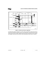
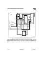
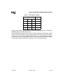
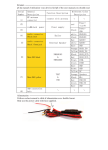
8XC251Sx
(8XC251SA, SB, SP, SQ)
SPECIFICATION UPDATE
Release Date: December, 1998
Order Number: 272836-007
Notice: The 8XC251Sx may contain design defects or errors known as errata.
Characterized errata that may cause the 8XC251Sx’s behavior to deviate from
published specifications are documented in this specification update.
Information in this document is provided in connection with Intel products. No license, express or implied, by estoppel or
otherwise, to any intellectual property rights is granted by this document. Except as provided in Intel’s Terms and Conditions of
Sale for such products, Intel assumes no liability whatsoever, and Intel disclaims any express or implied warranty, relating to sale
and/or use of Intel products including liability or warranties relating to fitness for a particular purpose, merchantability, or
infringement of any patent, copyright or other intellectual property right. Intel products are not intended for use in medical, life
saving, or life sustaining applications.
Intel may make changes to specifications and product descriptions at any time, without notice.
Designers must not rely on the absence or characteristics of any features or instructions marked "reserved" or "undefined." Intel
reserves these for future definition and shall have no responsibility whatsoever for conflicts or incompatibilities arising from future
changes to them.
The 8XC251Sx may contain design defects or errors known as errata which may cause the product to deviate from published
specifications. Current characterized errata are available on request.
Contact your local Intel sales office or your distributor to obtain the latest specifications and before placing your product order.
Copies of documents which have an ordering number and are referenced in this document, or other Intel literature may be
obtained by calling 1-800-548-4725 or by visiting Intel’s website at http://www.intel.com.
Copyright © Intel Corporation, 12/8/98
*Third-party brands and names are the property of their respective owners.
ii
December, 1998
272836-007
8XC251 SA/SB/SP/SQ SPECIFICATION UPDATE
CONTENTS
REVISION HISTORY .................................................................................1
PREFACE ..................................................................................................2
SUMMARY TABLE OF CHANGES ...........................................................4
IDENTIFICATION INFORMATION ............................................................6
ERRATA .....................................................................................................7
SPECIFICATION CHANGES ...................................................................15
SPECIFICATION CLARIFICATIONS ......................................................16
DOCUMENTATION CHANGES ...............................................................20
272836-007
December, 1998
iii
8XC251 SA/SB/SP/SQ SPECIFICATION UPDATE
REVISION HISTORY
Rev. Date Version
07/01/96
001
08/07/96
002
09/18/96
003
07/16/97
06/04/98
09/23/98
004
005
006
12/02/98
007
272936-007
Description
This is the new Specification Update document. It contains all
identified errata published prior to this date.
Added specification clarification, 001. Trdhz1 Timing.
Modified workaround for specification clarification number 001.
Trdhz1 Timing.
Modified the Affected Products section for erratum9700008.
Added Errata 9800009.
Added Errata 9800010.
Revised “Problem” text for Errata 9800010.
Added Document Changes 1 to 3.
December, 1998
1 of 20
8XC251 SA/SB/SP/SQ SPECIFICATION UPDATE
PREFACE
As of July, 1996, Intel’s Computing Enhancement Group has consolidated available
historical device and documentation errata into this new document type called the Specification Update. We have endeavored to include all documented errata in the consolidation
process, however, we make no representations or warranties concerning the
completeness of the Specification Update.
This document is an update to the specifications contained in the Affected
Documents/Related Documents table below. This document is a compilation of device and
documentation errata, specification clarifications and changes. It is intended for hardware
system manufacturers and software developers of applications, operating systems, or
tools.
Information types defined in Nomenclature are consolidated into the specification update
and are no longer published in other documents.
This document may also contain information that was not previously published.
Affected Documents/Related Documents
Title
8XC251SB Embedded Microcontroller User’s Manual
8XC251SA, 8XC251SB, 8XC251SP, 8XC251SQ Embedded
Microcontroller User’s Manual
Introducing the MCS® 251Microcontroller - the 8XC251SB
Maximizing Performance Using the MCS® 251 Microcontroller —
Programming the 8XC251SB
Migrating from the MCS® 51 Microcontroller to the MCS 251
Microcontroller (8XC251SB) — Software and Hardware Considerations
8XC251SA/SB/SP/SQ High Performance CHMOS Microcontroller
datasheet
2 of 20
December, 1998
Order
272617
272795
272670
272671
272672
272783
272936-007
8XC251 SA/SB/SP/SQ SPECIFICATION UPDATE
Nomenclature
Errata are design defects or errors. These may cause the published (component, board,
system) behavior to deviate from published specifications. Hardware and software
designed to be used with any component, board, and system must consider all errata
documented.
Specification Changes are modifications to the current published specifications. These
changes will be incorporated in any new release of the specification.
Specification Clarifications describe a specification in greater detail or further highlight
a specification’s impact to a complex design situation. These clarifications will be incorporated in any new release of the specification.
Documentation Changes include typos, errors, or omissions from the current published
specifications. These will be incorporated in any new release of the specification.
NOTE:Errata remain in the specification update throughout the product’s lifecycle,
or until a particular stepping is no longer commercially available. Under
these circumstances, errata removed from the specification update are
archived and available upon request. Specification changes, specification
clarifications and documentation changes are removed from the
specification update when the appropriate changes are made to the
appropriate product specification or user documentation (datasheets,
manuals, etc.).
272936-007
December, 1998
3 of 20
8XC251 SA/SB/SP/SQ SPECIFICATION UPDATE
SUMMARY TABLE OF CHANGES
The following table indicates the errata, specification changes, specification clarifications,
or documentation changes which apply to the 8XC251 SA/SB/SP/SQ product. Intel may
fix some of the errata in a future stepping of the component, and account for the other
outstanding issues through documentation or specification changes as noted. This table
uses the following notations:
Codes Used in Summary Table
Stepping
X:
Errata exists in the stepping indicated. Specification Change or Clarification that applies to this stepping.
(No mark)
or (Blank box):
This erratum is fixed in listed stepping or specification change does not
apply to listed stepping.
Page
(Page):
Page location of item in this document.
Status
Doc:
Document change or update will be implemented.
Fix:
This erratum is intended to be fixed in a future step of the component.
Fixed:
This erratum has been previously fixed.
NoFix:
There are no plans to fix this erratum.
Eval:
Plans to fix this erratum are under evaluation.
Row
Change bar to left of table row indicates this erratum is either new or
modified from the previous version of the document.
4 of 20
December, 1998
272936-007
8XC251 SA/SB/SP/SQ SPECIFICATION UPDATE
Errata
Steppings
A-1 B-1 C
9600001 X
9600002 X
Rev. #
Page Status
7
8
9600003
X
9
9600004
X
10
9600005
X
X
11
9600006
9600007
X
X
X
12
13
9700008
9800009
X
X
X
13
X
X
14
X
14
9800010
ERRATA
Fixed
Fixed
Negative Flag
WSB - Wait States for Memory Region 01
EJMP at Upper Boundary of Any 64K-Byte
Fixed
Region of Memory
Short Jumps from Memory Region FF: to
Fixed FE:
Interrupt when CPU is Executing User Code
Fix
Not in FF:Region
Fix
Carry Flag
Fix
Watchdog Timer in the Idle Mode
Data Memory Across 256-Byte Boundary
Fix
Region with INC DRK, #Short
Interrupts of Three or More Priority Levels
Fix
Occuring at the Same Time
NoFix EMAP# Function
Specification Changes
Rev. #
Steppings
#
#
#
Page Status
SPECIFICATION CHANGES
None for this revision of this specification update.
Specification Clarifications
Rev. #
001
Steppings
A-1 B-1 C
X
Page Status
16
Doc
SPECIFICATION CLARIFICATIONS
TRDHZ1 Timing.
Documentation Changes
Rev. #
1
2
3
272936-007
Document
Revision
272895-002
272617-001
272617-001
Page Status
20
20
20
Doc
Doc
Doc
DOCUMENTATION CHANGES
Page 6-2, Figure 6-1
Page 5-2, Figure 5-1
page 9-14, Section 9.6.3.4
December, 1998
5 of 20
8XC251 SA/SB/SP/SQ SPECIFICATION UPDATE
IDENTIFICATION INFORMATION
Markings
B-step devices are identified by the marking, Intel (R) (C) ‘94 ‘95 B.
C-step devices are identified by the marking Intel (R) (C) ’94 ’95 C.
6 of 20
December, 1998
272936-007
8XC251 SA/SB/SP/SQ SPECIFICATION UPDATE
ERRATA
9600001.
Negative Flag
PROBLEM: The Negative (N) Flag of PSW1 should be set or cleared corresponding to bit
15 of the result. Instead, it corresponds to bit 7 of the result.
IMPLICATION: The affected instructions are listed below:
a. SRL
WRj
b. SRA
WRj
c.
WRj
SLL
d. INC
WRj, #short
e. DEC
WRj, #short
WORKAROUND: There are two ways to work around this erratum:
1. Follow the affected instructions listed above with an operation that will rectify the
Negative (N) flag correctly. For example:
SRL WRj
ANL WRj, #0FFFFH
SLL Wrj
ANL WRj, WRj
2. b) Check bit 15 of the result vs. relying on the N flag for sign.
STATUS: Fixed. Refer to Summary Table of Changes to determine the affected
stepping(s).
AFFECTED PRODUCTS: (OPTIONAL) All the 8xC251SB devices on A-1 stepping are
affected.
272936-007
December, 1998
7 of 20
8XC251 SA/SB/SP/SQ SPECIFICATION UPDATE
9600002.
WSB - Wait States for Memory Region 01
PROBLEM: The WSb bit of configuration byte CONFIG1 is intended to configure 0 or 1
wait states for all MOVX (including MOVX @DPTR and MOVX @Ri) instructions for the
region 01:0000H-01:FFFFH. However, in 8XC251SB A-1 stepping devices, the MOVX
@Ri uses WSa of the configuration byte CONFIG0 instead of WSb.
IMPLICATION: The error affects the generating wait state by using WSb bit of configuration byte CONFIG0 during MOVX instruction at region 01:0000H to 01:FFFFH.
WORKAROUND: There are two ways to work around this erratum:
a. Configure both WSa and WSb bits with the same wait state if both MOVX
@DPTR and MOVX @Ri instructions are used and require the same wait state.
b. If it is required that WSb be configured different from WSa, then limit usage of the
MOVX instruction to the MOVX @DPTR format rather than the MOVX @Ri
format.
STATUS: Fixed. Refer to Summary Table of Changes to determine the affected
stepping(s).
AFFECTED PRODUCTS: All the 8xC251SB devices on A-1 stepping are affected.
8 of 20
December, 1998
272936-007
8XC251 SA/SB/SP/SQ SPECIFICATION UPDATE
9600003.
EJMP at Upper Boundary of Any 64K-Byte Region of Memory
PROBLEM: The EJMP instruction is intended for extended jumps from one 64K-byte
region of memory to another 64K-byte region of memory. However, when EJMP occurs at
the upper boundary of any 64K-byte region of memory, the Program Counter (PC) will
land in the wrong 64K-byte region of memory.
Example 2-1.
The code: “FEFFFD 8A00XXXX EJMP #00XXXXH”
should branch to address 00XXXXh, but it branches to address region 01XXXXh instead.
The operation of this instruction is shown below:
PC)
PC.23:16)
PC)
PC.15:0)
<---- (PC) + 2
<---- (Addr.23:16)
<---- (PC) + 2
<---- (Addr.15:0)
PC = FEFFFFh
PC = 00FFFFh
PC = 010001h*
PC = 01XXXXh
* Note: Overflow occurs when incrementing the PC for the lower two bytes of destination
address. The overflow has incremented the PC.23:16 and caused a deviation from the
destination Addr.23:16.
Instructions affected : EJMP
IMPLICATION: The erratum affects the function of EJMP instruction at the upper
boundary region.
WORKAROUND: Avoid this instruction being used at the upper boundary of any 64K-byte
memory region.
STATUS: Fixed. Refer to Summary Table of Changes to determine the affected
stepping(s).
AFFECTED PRODUCTS: All the 8xC251SB devices on A-1 stepping are affected.
272936-007
December, 1998
9 of 20
8XC251 SA/SB/SP/SQ SPECIFICATION UPDATE
9600004.
Short Jumps from Memory Region FF: to FE:
PROBLEM: The short jump instruction is intended for a +127 or -128 byte jump relative to
the current instruction. However, a short jump from the address in the lower boundary of
region FF: will not branch to the address in upper boundary of region FE: even though the
destination address is within this -128 byte range. Instead of landing at address in region
FE:, it will remain at address in region FF:.
Example:
The code with
“FEFFF0
FEFFF0 00
FF0002
FF0002 80EC
ORG FEFFF0h
REL_ADR: NOP
ORG FF0002h
SJMP REL_ADR”
should branch to address FEFFF0h, but it branches to address FFFFF0h in the same
region FF: instead.
IMPLICATION: Instructions affected : SJMP, CJNE, DJNZ, JB, JBC, JC, JE, JG, JLE,
JNB, JNC, JNE, JNZ, JSG, JSGE, JSL, JSLE, JZ
Please note that there is no errata for short jumps from upper boundary of region FE: to
lower boundary of region FF: ; and no errata for short jumps from upper boundary of
region 00: to lower boundary of region 01: and vice-versa.
WORKAROUND: Avoid these instructions being used for a short jump from the lower
boundary of region FF: to the upper boundary of region FE:
STATUS: Fixed. Refer to Summary Table of Changes to determine the affected
stepping(s).
AFFECTED PRODUCTS: All the 8xC251SB devices on A-1 stepping are affected.
10 of 20
December, 1998
272936-007
8XC251 SA/SB/SP/SQ SPECIFICATION UPDATE
9600005.
Interrupt when CPU is Executing User Code Not in FF:Region
PROBLEM: For 8XC251SB, the Reset Vector and Interrupt Vectors are defined at the FF:
region. If there is an interrupt occurs, the CPU is not able to jump to the Interrupt Vector
when the CPU is executing the user code at regions other than FF:.
Example:
If the user code size is 128K-Byte, the first 64K-Byte of the user code is located at FF:
region and the other 64K-Byte of the user code is located at FE: region. The Reset Vector
and Interrupt Vector for External Interrupt 0 (INT0) are defined at the FF: region as shown
below.
FF0000 02 0100
FF0003 02 0300
FF0100 12 0200
FF0300 C0D0
ORG FF:0000h
LJMP MAIN
ORG FF:0003h
LJMP EXT_INT0
ORG FF:0100h
MAIN: LCALL INITIALIZE_INT0
ORG FF:0300h
EXT_INT0: PUSH PSW
.
.
RETI
When the CPU is executing user code from FE: region, if an External Interrupt (INT0)
occurs, the CPU is not able to jump to Interrupt Vector (EXT_INT0) as defined at FF:
region.
IMPLICATION: This error affects additional interrupt vectors to be initialized at other
memory regions.
WORKAROUND: Bit 4 (INTR bit) of Configuration Byte (Config1) must be set to 1. All
needed Interrupt Vectors must be defined at other regions (other than FF: region) as well.
For an example, if the user code size is 128K-Byte and the first 64K-Byte of the user code
and the Interrupt Vector for External Interrupt 0 is defined at FF: region, that is
ORG FF:0003h
LJMP EXT_INT0
272936-007
December, 1998
11 of 20
8XC251 SA/SB/SP/SQ SPECIFICATION UPDATE
then there are two possible ways to locate the other 64K-Byte of user code and the
workaround:
1. If the other 64K-Byte of user code is located at FE: region, the following instructions
must be added to the user code at FE: region,
ORG FE:0003h
EJMP EXT_INT0
2. if the other 64K-Byte of user code is located at 00: region, the following instructions
must be added to the user code at 00: region.
ORG 00:0003h
EJMP EXT_INT0
STATUS: Fix. Refer to Summary Table of Changes to determine the affected stepping(s).
AFFECTED PRODUCTS: All the 8xC251SB A-1 and 8XC251SA/SB/SP/SQ B-1 stepping
devices are affected.
9600006.
Carry Flag
PROBLEM: The Carry (CY) Flag of PSW and PSW1 should be set or cleared corresponding to the last bit (bit 7) shifted out from a 8-bit Register after completion of the SLL
instruction.
After execution of this instruction, the Carry (CY) Flag is not set or cleared corresponding
to the last bit (bit 7) shifted out from a 8-bit Register.
IMPLICATION: The only affected instruction is listed below:
SLL Rm
WORKAROUND: Avoid this instruction.
STATUS: Fix. Refer to Summary Table of Changes to determine the affected stepping(s).
AFFECTED PRODUCTS: All the 8xC251SA/SB/SP/SQ devices on B-1 stepping are
affected.
12 of 20
December, 1998
272936-007
8XC251 SA/SB/SP/SQ SPECIFICATION UPDATE
9600007.
Watchdog Timer in the Idle Mode
PROBLEM: During the hardware or software WatchDog Timer operation in the Idle Mode,
it should RESET the controller and wake up from the Idle Mode after the counter overflow.
The controller fails to perform this operation.
IMPLICATION: This error affects the usage of hardware and software watchdog timer
during the idle mode.
WORKAROUND: There is no workaround for this erratum. This erratum is fixed in the
8XC251SA/SB/SP/SQ next stepping (C stepping).
STATUS: Fix. Refer to Summary Table of Changes to determine the affected stepping(s).
AFFECTED PRODUCTS: All the 8xC251SB
8XC251SA/SB/SP/SQ B-1 stepping are affected.
9700008.
devices
on
A-1
stepping
and
Data Memory Across 256-Byte Boundary Region with INC DRK,
#Short
PROBLEM: When the DRk register contains the address for data memory, the INC DRk,
#short instructions — where short is either 1, 2 or 4 — do not work across the 256Bytes
(FFH) boundary region.
Example:
If the content of DR4 register is 0000 00FEH, which is the address for data memory, the
following instructions:
INC DR4, #2H
should increase the content of DR4 register, i.e., data memory address to 0000 0100H.
However, the DR4 register does not contain 00000100H.
IMPLICATION: This error affects the instructions INC DRk, #short.
WORKAROUND: Replace INC DRk, #short with ADD DRk, #short.
Example:
By using the same example shown above, the workaround should be
ADD DR4, #2H
STATUS: Fix. Refer to Summary Table of Changes to determine the affected stepping(s).
AFFECTED PRODUCTS: All 8xC251SA/SB/SP/SQ devices on B-1 and C steppings.
272936-007
December, 1998
13 of 20
8XC251 SA/SB/SP/SQ SPECIFICATION UPDATE
9800009
Interrupts of Three or More Priority Levels Occuring at the Same
Time
PROBLEM: When three or more interrupts of different priorities occur at approximately
the same time (~40 ns window) on the 8xC251Sx, the lowest priority interrupt will not be
serviced correctly. As the lower priority interrupt is interrupted by a higher priority interrupt,
the interrupt pending bit remains set and the device believes it is still servicing the lowest
priority interrupt. This disables any further lowest priority interrupt from being serviced.
Any interrupt source can be affected by this if it is the lowest priority of the three enabled
interrupts. For example, if external interrupt 0 is priority 3, timer 1 is priority 2 the and
serial port is priority 0, and all three interrupts occur at the same time, then the serial port
interrupt would stop being serviced.
IMPLICATION: This will cause the lowest priority interrupt to no longer be serviced and
the interrupt will not recover unless a device reset occurs
WORKAROUND: To ensure this interrupt priority conflict does not occur, make sure only
two interrupt priority levels are enabled at any given time
STATUS: Fix. Refer to Summary Table of Changes to determine the affected stepping(s).
9800010
EMAP# Function
PROBLEM: The EMAP# bit of the configuration byte is intended to map the upper half of
the on-chip code memory (region FF:2000H - FF:3FFFH to region 00:E000H - 00:FFFFH).
However, when data is retrieved from region 00:E000H - 00:FFFFH by use of the read
instructions, data from incorrect addresses are retrieved.
IMPLICATION: The erratum affects the function of the EMAP# bit at the upper half of
on-chip code memory.
WORKAROUND: There are two ways to workaround this erratum:
1. Directly read the data from region FF:2000H - FF:3FFFH by using instruction
MOV A,@DR0 instead of reading from region 00:E000H - 00:FFFFH.
2. Use instruction MOVC A,@A+DPTR to directly read the data from region
FF:2000H - FF:3FFFH. The limitation for this instruction is that it can only be used to
read 256 bytes of data continuously.
STATUS: NoFix. Refer to Summary Table of Changes to determine the affected
stepping(s).
AFFECTED PRODUCTS: 87C251SB,SQ and 83C251SB,SQ devices on C-Stepping are
affected.
14 of 20
December, 1998
272936-007
8XC251 SA/SB/SP/SQ SPECIFICATION UPDATE
SPECIFICATION CHANGES
None for this revision of this specification update.
272936-007
December, 1998
15 of 20
8XC251 SA/SB/SP/SQ SPECIFICATION UPDATE
SPECIFICATION CLARIFICATIONS
001.
Trdhz1 Timing.
PROBLEM: The TRHDZ1 (Instruction Float After RD#/PSEN# High) specification on the
8XC251Sx when operating at 12 MHz is 10 ns. However, a slow memory device such as
an EPROM typically takes approximately 30 – 90 ns to float its output. (This specification
generically called TPHZ, may vary from one manufacturer to another.) and illustrate the
TRHDZ1 timing.
The difference between the TRHDZ1 and TPHZ specifications causes contention on the
data bus (P0 in nonpage page, P2 in page mode). The 8XC251Sx begins to drive the
address for the next bus cycle while the memory device is still driving data from the
previous bus cycle.
State 1
State 2
State 1
(next cycle)
ALE
TLHLL
RD#\PSEN#
TLLRL
TRLRH
TAVLL
TRLAZ
TAVRL
TRLDV
TRHDX
TRHDZ1
TLLAX
TLHAX
P0
TRHLH1
A7:0
Instruction In
TAVDV1
A17/A16/P2
A17/A16/A15:8
TAVDV2
A5011-01
Figure 1. External Code Fetch, Nonpage Mode
16 of 20
December, 1998
272936-007
8XC251 SA/SB/SP/SQ SPECIFICATION UPDATE
State 1
Cycle 1, Page Miss
State 2
Cycle 2, Page Hit
State 1
ALE
TLHLL
RD#\PSEN#
TLLRL
TRLDV
TRHDX
TLLAX
TLHAX
TRHDZ1
A15:8
Instruction 1 In
TAVDV1
A17/A16/P0
†
TAVLL
TRLAZ
TAVRL
P2
TRHLH1
TRLRH
Instruction 2 In
TAVDV3
A17/A16/A7:0
TAVDV2
† During a sequence of page hits, PSEN# remains low until the end of the last page hit cycle.
A5028-02
Figure 2. External Code Fetch, Page Mode
To prevent this contention, designers can use a buffer to isolate the output of the memory
device from the data bus (port 0 or port 2) of the 8XC251Sx. This will prevent the slow
memory device from driving the data bus during the critical period after TRHDZ1 expires.
We suggest a buffer such as the 74F541 octal, three-state line driver shown in Figure 3.
272936-007
December, 1998
17 of 20
8XC251 SA/SB/SP/SQ SPECIFICATION UPDATE
AD7:0
P0.7:0
D8:1
ALE
LE
OE#
Q8:1
A7:0
Q8:1
A7:0
74AC373
P2.7:0
74AC04
P3.6/WR#
P3.7/RD#/A16
CS2#
A15:8
A15:8
A16
CE#
OE#
A16
CS1#
OE#
WE#
128K
RAM
128K
EPROM
PSEN#
P1.7/CEX4
/A17/WCLK
8XC251Sx
D7:0
VCC
A16
PSEN#
PSEN#
A16
A17
A17
WR#
OE2#
OE1#
D7:0
Y7:0
A7:1
74F541
A5111-02
Figure 3. Example Bus Contention Solution for 8XC251Sx
Figure 3 illustrates the connections of an 8XC251Sx configured for nonpage mode with
EPROM and RAM in external memory. If your system uses a different configuration, your
circuit will be different from the example. The 74F541 is enabled to pass data from the
EPROM to the 8XC251Sx (port 0) when OE1# and OE2# are active. Table 1 is a truth
table for the 74F541.
18 of 20
December, 1998
272936-007
8XC251 SA/SB/SP/SQ SPECIFICATION UPDATE
Table 1. Truth Table for 74F541
Inputs
Outputs
OE1#
OE2#
A7:1
Y7:1
L
L
L
L
L
L
H
H
X
H
X
Z
H
X
X
Z
During a read, PSEN# turns the buffer on (OE1# and OE2# are active), connecting the
EPROM’s output to the 8XC251Sx’s port 0.
When PSEN# goes high after a read, 1G# and 2G# are deasserted and the buffer’s output
switches to the high-impedance state in approximately 9.5 ns (TPHZ for a typical 74F541;
the value may vary from one manufacturer to another). Thus, contention on the data bus
is prevented. This or a similar hardware solution is recommended for 8XC251Sx designs
in which slower memory devices do not meet the TRHDZ1 timing specification.
272936-007
December, 1998
19 of 20
8XC251 SA/SB/SP/SQ SPECIFICATION UPDATE
DOCUMENTATION CHANGES
1.
Page 6-2, Figure 6-1
PROBLEM: Interrupt System Error:
•
The PCA, Serial, and Timer2 Interrupts have been wrongly placed in the diagram,
according to their interrupt priority-within-level. The correct placement is after the
Timer1 interrupt. The next sequence should be Serial interrupt, followed by Timer2,
and then PCA interrupt.
AFFECTED PRODUCTS: 8XC251SA, 8XC251SB, 8XC251SP, 8XC251SQ Embedded
Microcontroller User’s Manual.
2.
Page 5-2, Figure 5-1
PROBLEM: Interrupt System Error:
•
The PCA, Serial, and Timer2 Interrupts have been wrongly placed in the diagram,
according to their interrupt priority-within-level. The correct placement is after the
Timer1 interrupt. The next sequence should be Serial interrupt, followed by Timer2,
and then PCA interrupt.
AFFECTED PRODUCTS: 8XC251SB Embedded Microcontroller User’s Manual.
3.
page 9-14, Section 9.6.3.4
PROBLEM: Serial I/O Port Error:
•
There is an equation to calculate the baud rate of the serial port. In the denominator,
the manual wrongly states “32 X [553 - (RCAP2H,RCAP2L)]”. It should state “32 X
[65536 - (RCAP2H,RCAP2L)]”.
AFFECTED PRODUCTS: 8XC251SB Embedded Microcontroller User’s Manual.
20 of 20
December, 1998
272936-007