1
Freescale Semiconductor
Data Sheet: Technical Data
Document Number: DSP56367
Rev. 2.1, 1/2007
DSP56367
24-Bit Audio Digital Signal Processor
1
Overview
This document briefly describes the DSP56367 24-bit
digital signal processor (DSP). The DSP56367 is a
member of the DSP56300 family of programmable
CMOS DSPs. The DSP56367 is targeted to applications
that require digital audio compression/decompression,
sound field processing, acoustic equalization and other
digital audio algorithms. The DSP56367 offers 150
million instructions per second (MIPS) using an internal
150 MHz clock at 1.8 V and 100 million instructions per
second (MIPS) using an internal 100 MHz clock at 1.5 V.
Contents
1
2
3
4
5
A
Overview . . . . . . . . . . . . . . . . . . . . . . . . . . . .
Signal/Connection Descriptions . . . . . . . . . . .
Specifications . . . . . . . . . . . . . . . . . . . . . . . . .
Packaging. . . . . . . . . . . . . . . . . . . . . . . . . . . .
Design Considerations . . . . . . . . . . . . . . . . . .
Power Consumption Benchmark . . . . . . . . . .
1-1
2-1
3-1
4-1
5-1
A-1
This document contains information on a new product. Specifications and information herein are subject to change without notice.
© Freescale Semiconductor, Inc., 2001, 2002, 2003, 2004, 2005, 2006, 2007. All rights reserved.
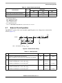
Overview
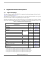
Data Sheet Conventions
This data sheet uses the following conventions:
OVERBAR
Used to indicate a signal that is active when pulled low (For example, the RESET pin is active
when low.)
“asserted”
Means that a high true (active high) signal is high or that a low true (active low) signal is low
“deasserted”
Means that a high true (active high) signal is low or that a low true (active low) signal is high
Examples:
Signal/Symbol
Logic State
Signal State
Voltage*
PIN
True
Asserted
VIL / VOL
PIN
False
Deasserted
VIH / VOH
PIN
True
Asserted
VIH / VOH
PIN
False
Deasserted
VIL / VOL
Note:*Values for VIL, VOL, VIH, and VOH are defined by individual product specifications.
8
16
2
1
4
5
6
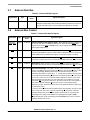
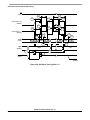
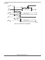
MEMORY EXPANSION AREA
SHI
INTERFACE
ADDRESS
GENERATION
UNIT
PIO_EB
ESAI_1
PERIPHERAL
EXPANSION AREA
SIX CHANNELS
DMA UNIT
X
MEMORY
RAM
13K X 24
ROM
32K x 24
YAB
XAB
PAB
DAB
Y
MEMORY
RAM
7K X 24
ROM
8K x 24
YM_EB
ESAI
INTERFACE
XM_EB
HOST
INTERFACE
PROGRAM
RAM
/INSTR. CACHE
3K x 24
PROGRAM
ROM
40K x 24
Bootstrap ROM
192 x 24
PM_EB
TRIPLE
TIMER
DAX
(SPDIF Tx.)
INTERFACE
EXTERNAL
ADDRESS
BUS
SWITCH
24-BIT
DSP56300
Core
DRAM &
SRAM BUS
INTERFACE
&
I - CACHE
18
ADDRESS
10
CONTROL
DDB
YDB
INTERNAL
DATA
BUS
SWITCH
EXTERNAL
DATA BUS
SWITCH
XDB
PDB
24
DATA
GDB
POWER
MNGMNT
PLL
CLOCK
GENERATOR
EXTAL
RESET
PINIT/NMI
PROGRAM
INTERRUPT
CONTROLLER
PROGRAM
DECODE
CONTROLLE
PROGRAM
ADDRESS
GENERATOR
DATA ALU
24X24+56->56-BIT MAC
TWO 56-BIT ACCUMULATORS
BARREL SHIFTER
MODA/IRQA
MODB/IRQB
MODC/IRQC
MODD/IRQD
JTAG
4
OnCE™
24 BITS BUS
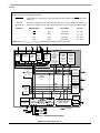
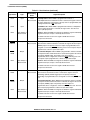
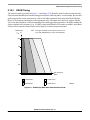
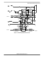
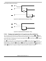
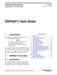
Figure 1-1 DSP56367 Block Diagram
DSP56367 Technical Data, Rev. 2.1
1-2
Freescale Semiconductor
Overview
1.1
Features
Core features are described fully in the DSP56300 Family Manual.
1.2
•
•
•
•
•
•
•
•
•
•
•
1.3
•
•
•
•
•
1.4
•
•
•
•
1.5
•
DSP56300 modular chassis
150 Million Instructions Per Second (MIPS) with a 150 MHz clock at internal logic supply
(QVCCL) of 1.8V.
100 Million Instructions Per Second (MIPS) with a 100 MHz clock at internal logic supply
(QVCCL) of 1.5V.
Object Code Compatible with the 56K core.
Data ALU with a 24 × 24 bit multiplier-accumulator and a 56-bit barrel shifter. 16-bit arithmetic
support.
Program Control with position independent code support and instruction cache support.
Six-channel DMA controller.
PLL based clocking with a wide range of frequency multiplications (1 to 4096), predivider factors
(1 to 16) and power saving clock divider (2i: i=0 to 7). Reduces clock noise.
Internal address tracing support and OnCE™ for Hardware/Software debugging.
JTAG port.
Very low-power CMOS design, fully static design with operating frequencies down to DC.
STOP and WAIT low-power standby modes.
On-chip Memory Configuration
7K × 24 Bit Y-Data RAM and 8K × 24 Bit Y-Data ROM.
13K × 24 Bit X-Data RAM and 32K × 24 Bit X-Data ROM.
40K × 24 Bit Program ROM.
3K × 24 Bit Program RAM and 192x24 Bit Bootstrap ROM. 1K of Program RAM may be used as
Instruction Cache or for Program ROM patching.
2K × 24 Bit from Y Data RAM and 5K × 24 Bit from X Data RAM can be switched to Program
RAM resulting in up to 10K × 24 Bit of Program RAM.
Off-chip memory expansion
External Memory Expansion Port.
Off-chip expansion up to two 16M x 24-bit word of Data memory.
Off-chip expansion up to 16M x 24-bit word of Program memory.
Simultaneous glueless interface to SRAM and DRAM.
Peripheral modules
Serial Audio Interface (ESAI): up to 4 receivers and up to 6 transmitters, master or slave. I2S, Sony,
AC97, network and other programmable protocols.
DSP56367 Technical Data, Rev. 2.1
Freescale Semiconductor
1-3
Overview
•
•
•
•
•
•
Serial Audio Interface I(ESAI_1): up to 4 receivers and up to 6 transmitters, master or slave. I2S,
Sony, AC97, network and other programmable protocols
The ESAI_1 shares four of the data pins with ESAI, and ESAI_1 does NOT support HCKR and
HCKT (high frequency clocks)
Serial Host Interface (SHI): SPI and I2C protocols, multi master capability, 10-word receive FIFO,
support for 8, 16 and 24-bit words.
Byte-wide parallel Host Interface (HDI08) with DMA support.
Triple Timer module (TEC).
Digital Audio Transmitter (DAX): 1 serial transmitter capable of supporting the SPDIF, IEC958,
CP-340 and AES/EBU digital audio formats.
Pins of unused peripherals (except SHI) may be programmed as GPIO lines.
1.6
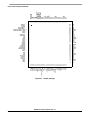
144-pin plastic LQFP package
1.7
Documentation
Table 1-1 lists the documents that provide a complete description of the DSP56367 and are required to
design properly with the part. Documentation is available from a local Freescale distributor, a Freescale
semiconductor sales office, a Freescale Literature Distribution Center, or through the Freescale DSP home
page on the Internet (the source for the latest information).
Table 1-1 DSP56367 Documentation
Document Name
Description
Order Number
DSP56300 Family Manual
Detailed description of the 56000-family architecture
and the 24-bit core processor and instruction set
DSP56300FM
DSP56367 Product Brief
Brief description of the chip
DSP56367 User’s Manual
DSP56367 User’s Manual
DSP56367 Technical Data Sheet
(this document)
Electrical and timing specifications; pin and package
descriptions
IBIS Model
Input Output Buffer Information Specification
DSP56367P
DSP56367UM
DSP56367
For software or simulation
models, contact sales or
go to www.freescale.com.
DSP56367 Technical Data, Rev. 2.1
1-4
Freescale Semiconductor
2
Signal/Connection Descriptions
2.1
Signal Groupings
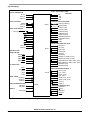
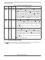
The input and output signals of the DSP56367 are organized into functional groups, which are listed in
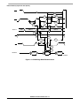
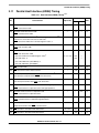
Table 2-1 and illustrated in Figure 2-1.
The DSP56367 is operated from a 1.8V supply; however, some of the inputs can tolerate 3.3V. A special
notice for this feature is added to the signal descriptions of those inputs.
Remember, the DSP56367 offers 150 million instructions per second (MIPS) using an internal 150 MHz
clock at 1.8 V and 100 million instructions per second (MIPS) using an internal 100 MHz clock at 1.3.3V.
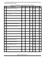
Table 2-1 DSP56367 Functional Signal Groupings
Number of
Signals
Detailed
Description
Power (VCC)
20
Table 2-2
Ground (GND)
18
Table 2-3
Clock and PLL
3
Table 2-4
18
Table 2-5
24
Table 2-6
Bus control
10
Table 2-7
Interrupt and mode control
5
Table 2-8
16
Table 2-9
5
Table 2-10
Functional Group
Address bus
Data bus
HDI08
Port A
1
Port B2
SHI
ESAI
Port C3
12
Table 2-11
ESAI_1
Port E4
6
Table 2-12
Digital audio transmitter (DAX)
Port D5
2
Table 2-13
Timer
1
Table 2-14
JTAG/OnCE Port
4
Table 2-15
1
Port A is the external memory interface port, including the external address bus, data bus, and control signals.
Port B signals are the GPIO port signals which are multiplexed with the HDI08 signals.
3 Port C signals are the GPIO port signals which are multiplexed with the ESAI signals.
4 Port E signals are the GPIO port signals which are multiplexed with the ESAI_1 signals.
5 Port D signals are the GPIO port signals which are multiplexed with the DAX signals.
2
DSP56367 Technical Data, Rev. 2.1
Freescale Semiconductor
2-1
Signal Groupings
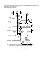
OnCE‰ ON-CHIP EMULATION/
JTAG PORT
TDI
PORT A ADDRESS BUS
A0-A17
VCCA (3)
DSP56367
TCK
TDO
TMS
GNDA (4)
PORT A DATA BUS
PARALLEL HOST PORT (HDI08)
D0-D23
VCCD (4)
HAD(7:0) [PB0-PB7]
Port B
HAS/HA0 [PB8]
GNDD (4)
HA8/HA1 [PB9]
PORT A BUS CONTROL
HA9/HA2 [PB10]
AA0-AA2/RAS0-RAS2
HRW/HRD [PB11]
CAS
HDS/HWR [PB12]
RD
HCS/HA10 [PB13]
WR
HOREQ/HTRQ [PB14]
TA
HACK/HRRQ [PB15]
VCCH
GNDH
BR
BG
SERIAL AUDIO INTERFACE (ESAI)
BB
SCKT[PC3]
VCCC (2)
GNDC (2)
FST [PC4]
Port C
HCKT [PC5]
INTERRUPT AND
SCKR [PC0]
MODE CONTROL
FSR [PC1]
MODA/IRQA
HCKR [PC2]
MODB/IRQB
SDO0[PC11] / SDO0_1[PE11]
MODC/IRQC
SDO1[PC10] / SDO1_1[PE10]
MODD/IRQD
SDO2/SDI3[PC9] / SDO2_1/SDI3_1[PE9]
RESET
SDO3/SDI2[PC8] / SDO3_1/SDI2_1[PE8]
SDO4/SDI1 [PC7]
PLL AND CLOCK
SDO5/SDI0 [PC6]
EXTAL
PINIT/NMI
PCAP
SERIAL AUDIO INTERFACE(ESAI_1)
SCKT_1[PE3]
VCCP
FS T_1[PE4]
Port E
SCKR_1[PE0]
GNDP
FSR_1[PE1]
QUIET POWER
VCCQH (3)
SDO4_1/SDI1_1[PE7]
VCCQL (4)
GNDQ (4)
SDO5_1/SDI0_1[PE6]
VCCS (2)
GNDS (2)
SPDIF TRANSMITTER (DAX)
ADO [PD1]
Port D
SERIAL HOST INTERFACE (SHI)
ACI [PD0]
MOSI/HA0
TIO0 [TIO0]
SS/HA2
MISO/SDA
TIMER 0
SCK/SCL
HREQ
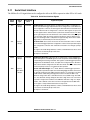
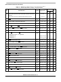
Figure 2-1 Signals Identified by Functional Group
DSP56367 Technical Data, Rev. 2.1
2-2
Freescale Semiconductor
Power
2.2
Power
Table 2-2 Power Inputs
Power Name
Description
VCCP
PLL Power—VCCP is VCC dedicated for PLL use. The voltage should be well-regulated and the input should
be provided with an extremely low impedance path to the VCC power rail. There is one VCCP input.
VCCQL (4)
Quiet Core (Low) Power—VCCQL is an isolated power for the internal processing logic. This input must be
tied externally to all other VCCQL power pins and the VCCP power pin only. Do not tie with other power pins.
The user must provide adequate external decoupling capacitors. There are four VCCQL inputs.
VCCQH (3)
Quiet External (High) Power—VCCQH is a quiet power source for I/O lines. This input must be tied externally
to all other chip power inputs.The user must provide adequate decoupling capacitors. There are three VCCQH
inputs.
VCCA (3)
Address Bus Power—VCCA is an isolated power for sections of the address bus I/O drivers. This input must
be tied externally to all other chip power inputs. The user must provide adequate external decoupling
capacitors. There are three VCCA inputs.
VCCD (4)
Data Bus Power—VCCD is an isolated power for sections of the data bus I/O drivers. This input must be tied
externally to all other chip power inputs. The user must provide adequate external decoupling capacitors.
There are four VCCD inputs.
VCCC (2)
Bus Control Power—VCCC is an isolated power for the bus control I/O drivers. This input must be tied
externally to all other chip power inputs. The user must provide adequate external decoupling capacitors.
There are two VCCC inputs.
VCCH
Host Power—VCCH is an isolated power for the HDI08 I/O drivers. This input must be tied externally to all
other chip power inputs. The user must provide adequate external decoupling capacitors. There is one VCCH
input.
VCCS (2)
SHI, ESAI, ESAI_1, DAX and Timer Power —VCCS is an isolated power for the SHI, ESAI, ESAI_1, DAX
and Timer. This input must be tied externally to all other chip power inputs. The user must provide adequate
external decoupling capacitors. There are two VCCS inputs.
2.3
Ground
Table 2-3 Grounds
Ground Name
Description
GNDP
PLL Ground—GNDP is a ground dedicated for PLL use. The connection should be provided with an
extremely low-impedance path to ground. VCCP should be bypassed to GNDP by a 0.47 µF capacitor located
as close as possible to the chip package. There is one GNDP connection.
GNDQ (4)
Quiet Ground—GNDQ is an isolated ground for the internal processing logic. This connection must be tied
externally to all other chip ground connections. The user must provide adequate external decoupling
capacitors. There are four GNDQ connections.
GNDA (4)
Address Bus Ground—GNDA is an isolated ground for sections of the address bus I/O drivers. This
connection must be tied externally to all other chip ground connections. The user must provide adequate
external decoupling capacitors. There are four GNDA connections.
GNDD (4)
Data Bus Ground—GNDD is an isolated ground for sections of the data bus I/O drivers. This connection
must be tied externally to all other chip ground connections. The user must provide adequate external
decoupling capacitors. There are four GNDD connections.
DSP56367 Technical Data, Rev. 2.1
Freescale Semiconductor
2-3
Clock and PLL
Table 2-3 Grounds (continued)
Ground Name
Description
GNDC (2)
Bus Control Ground—GNDC is an isolated ground for the bus control I/O drivers. This connection must be
tied externally to all other chip ground connections. The user must provide adequate external decoupling
capacitors. There are two GNDC connections.
GNDH
Host Ground—GNDh is an isolated ground for the HD08 I/O drivers. This connection must be tied externally
to all other chip ground connections. The user must provide adequate external decoupling capacitors. There
is one GNDH connection.
GNDS (2)
SHI, ESAI, ESAI_1, DAX and Timer Ground—GNDS is an isolated ground for the SHI, ESAI, ESAI_1, DAX
and Timer. This connection must be tied externally to all other chip ground connections. The user must
provide adequate external decoupling capacitors. There are two GNDS connections.
2.4
Clock and PLL
Table 2-4 Clock and PLL Signals
Signal Name
Type
State During
Reset
EXTAL
Input
Input
External Clock Input—An external clock source must be connected to EXTAL in
order to supply the clock to the internal clock generator and PLL.
PCAP
Input
Input
PLL Capacitor—PCAP is an input connecting an off-chip capacitor to the PLL filter.
Connect one capacitor terminal to PCAP and the other terminal to VCCP.
Signal Description
If the PLL is not used, PCAP may be tied to VCC, GND, or left floating.
PINIT/NMI
2.5
Input
Input
PLL Initial/Nonmaskable Interrupt—During assertion of RESET, the value of
PINIT/NMI is written into the PLL Enable (PEN) bit of the PLL control register,
determining whether the PLL is enabled or disabled. After RESET de assertion and
during normal instruction processing, the PINIT/NMI Schmitt-trigger input is a
negative-edge-triggered nonmaskable interrupt (NMI) request internally synchronized
to internal system clock.
External Memory Expansion Port (Port A)
When the DSP56367 enters a low-power standby mode (stop or wait), it releases bus mastership and
tri-states the relevant port A signals: A0–A17, D0–D23, AA0/RAS0–AA2/RAS2, RD, WR, BB, CAS.
2.6
External Address Bus
Table 2-5 External Address Bus Signals
Signal Name
Type
State During
Reset
A0–A17
Output
Tri-Stated
Signal Description
Address Bus—When the DSP is the bus master, A0–A17 are active-high outputs
that specify the address for external program and data memory accesses. Otherwise,
the signals are tri-stated. To minimize power dissipation, A0–A17 do not change state
when external memory spaces are not being accessed.
DSP56367 Technical Data, Rev. 2.1
2-4
Freescale Semiconductor
External Data Bus
2.7
External Data Bus
Table 2-6 External Data Bus Signals
Signal Name
Type
State during
Reset
D0–D23
Input/Output
Tri-Stated
2.8
Signal Description
Data Bus—When the DSP is the bus master, D0–D23 are active-high,
bidirectional input/outputs that provide the bidirectional data bus for external
program and data memory accesses. Otherwise, D0–D23 are tri-stated.
External Bus Control
Table 2-7 External Bus Control Signals
Signal Name
Type
State During
Reset
AA0–AA2/
RAS0–RAS2
Output
Tri-Stated
Address Attribute or Row Address Strobe—When defined as AA, these signals can
be used as chip selects or additional address lines. When defined as RAS, these
signals can be used as RAS for DRAM interface. These signals are tri-statable outputs
with programmable polarity.
CAS
Output
Tri-Stated
Column Address Strobe— When the DSP is the bus master, CAS is an active-low
output used by DRAM to strobe the column address. Otherwise, if the bus mastership
enable (BME) bit in the DRAM control register is cleared, the signal is tri-stated.
RD
Output
Tri-Stated
Read Enable—When the DSP is the bus master, RD is an active-low output that is
asserted to read external memory on the data bus (D0-D23). Otherwise, RD is tri-stated.
WR
Output
Tri-Stated
Write Enable—When the DSP is the bus master, WR is an active-low output that is
asserted to write external memory on the data bus (D0-D23). Otherwise, WR is tri-stated.
TA
Input
Signal Description
Ignored Input Transfer Acknowledge—If the DSP is the bus master and there is no external bus
activity, or the DSP is not the bus master, the TA input is ignored. The TA input is a data
transfer acknowledge (DTACK) function that can extend an external bus cycle
indefinitely. Any number of wait states (1, 2. . .infinity) may be added to the wait states
inserted by the BCR by keeping TA deasserted. In typical operation, TA is deasserted
at the start of a bus cycle, is asserted to enable completion of the bus cycle, and is
deasserted before the next bus cycle. The current bus cycle completes one clock
period after TA is asserted synchronous to the internal system clock. The number of
wait states is determined by the TA input or by the bus control register (BCR),
whichever is longer. The BCR can be used to set the minimum number of wait states
in external bus cycles.
In order to use the TA functionality, the BCR must be programmed to at least one wait
state. A zero wait state access cannot be extended by TA deassertion, otherwise
improper operation may result. TA can operate synchronously or asynchronously,
depending on the setting of the TAS bit in the operating mode register (OMR).
TA functionality may not be used while performing DRAM type accesses, otherwise
improper operation may result.
DSP56367 Technical Data, Rev. 2.1
Freescale Semiconductor
2-5
Interrupt and Mode Control
Table 2-7 External Bus Control Signals (continued)
State During
Reset
Signal Name
Type
Signal Description
BR
Output
Output
Bus Request—BR is an active-low output, never tri-stated. BR is asserted when the
(deasserted) DSP requests bus mastership. BR is deasserted when the DSP no longer needs the
bus. BR may be asserted or deasserted independent of whether the DSP56367 is a
bus master or a bus slave. Bus “parking” allows BR to be deasserted even though the
DSP56367 is the bus master. (See the description of bus “parking” in the BB signal
description.) The bus request hold (BRH) bit in the BCR allows BR to be asserted under
software control even though the DSP does not need the bus. BR is typically sent to an
external bus arbitrator that controls the priority, parking, and tenure of each master on
the same external bus. BR is only affected by DSP requests for the external bus, never
for the internal bus. During hardware reset, BR is deasserted and the arbitration is reset
to the bus slave state.
BG
Input
Ignored Input Bus Grant—BG is an active-low input. BG is asserted by an external bus arbitration
circuit when the DSP56367 becomes the next bus master. When BG is asserted, the
DSP56367 must wait until BB is deasserted before taking bus mastership. When BG is
deasserted, bus mastership is typically given up at the end of the current bus cycle.
This may occur in the middle of an instruction that requires more than one external bus
cycle for execution.
For proper BG operation, the asynchronous bus arbitration enable bit (ABE) in the
OMR register must be set.
BB
Input/
Output
Input
Bus Busy—BB is a bidirectional active-low input/output. BB indicates that the bus is
active. Only after BB is deasserted can the pending bus master become the bus master
(and then assert the signal again). The bus master may keep BB asserted after ceasing
bus activity regardless of whether BR is asserted or deasserted. This is called “bus
parking” and allows the current bus master to reuse the bus without rearbitration until
another device requires the bus. The deassertion of BB is done by an “active pull-up”
method (i.e., BB is driven high and then released and held high by an external pull-up
resistor).
For proper BB operation, the asynchronous bus arbitration enable bit (ABE) in the OMR
register must be set.
BB requires an external pull-up resistor.
2.9
Interrupt and Mode Control
The interrupt and mode control signals select the chip’s operating mode as it comes out of hardware reset.
After RESET is deasserted, these inputs are hardware interrupt request lines.
DSP56367 Technical Data, Rev. 2.1
2-6
Freescale Semiconductor
Interrupt and Mode Control
Table 2-8 Interrupt and Mode Control
Signal Name
Type
State During
Reset
MODA/IRQA
Input
Input
Signal Description
Mode Select A/External Interrupt Request A—MODA/IRQA is an active-low
Schmitt-trigger input, internally synchronized to the DSP clock. MODA/IRQA selects
the initial chip operating mode during hardware reset and becomes a level-sensitive or
negative-edge-triggered, maskable interrupt request input during normal instruction
processing. MODA, MODB, MODC, and MODD select one of 16 initial chip operating
modes, latched into the OMR when the RESET signal is deasserted. If the processor
is in the stop standby state and the MODA/IRQA pin is pulled to GND, the processor
will exit the stop state.
This input is 3.3V tolerant.
MODB/IRQB
Input
Input
Mode Select B/External Interrupt Request B—MODB/IRQB is an active-low
Schmitt-trigger input, internally synchronized to the DSP clock. MODB/IRQB selects
the initial chip operating mode during hardware reset and becomes a level-sensitive or
negative-edge-triggered, maskable interrupt request input during normal instruction
processing. MODA, MODB, MODC, and MODD select one of 16 initial chip operating
modes, latched into OMR when the RESET signal is deasserted.
This input is 3.3V tolerant.
MODC/IRQC
Input
Input
Mode Select C/External Interrupt Request C—MODC/IRQC is an active-low
Schmitt-trigger input, internally synchronized to the DSP clock. MODC/IRQC selects
the initial chip operating mode during hardware reset and becomes a level-sensitive or
negative-edge-triggered, maskable interrupt request input during normal instruction
processing. MODA, MODB, MODC, and MODD select one of 16 initial chip operating
modes, latched into OMR when the RESET signal is deasserted.
This input is 3.3V tolerant.
MODD/IRQD
Input
Input
Mode Select D/External Interrupt Request D—MODD/IRQD is an active-low
Schmitt-trigger input, internally synchronized to the DSP clock. MODD/IRQD selects
the initial chip operating mode during hardware reset and becomes a level-sensitive or
negative-edge-triggered, maskable interrupt request input during normal instruction
processing. MODA, MODB, MODC, and MODD select one of 16 initial chip operating
modes, latched into OMR when the RESET signal is deasserted.
This input is 3.3V tolerant.
RESET
Input
Input
Reset—RESET is an active-low, Schmitt-trigger input. When asserted, the chip is
placed in the Reset state and the internal phase generator is reset. The Schmitt-trigger
input allows a slowly rising input (such as a capacitor charging) to reset the chip reliably.
When the RESET signal is deasserted, the initial chip operating mode is latched from
the MODA, MODB, MODC, and MODD inputs. The RESET signal must be asserted
during power up. A stable EXTAL signal must be supplied while RESET is being
asserted.
This input is 3.3V tolerant.
DSP56367 Technical Data, Rev. 2.1
Freescale Semiconductor
2-7
Parallel Host Interface (HDI08)
2.10
Parallel Host Interface (HDI08)
The HDI08 provides a fast, 8-bit, parallel data port that may be connected directly to the host bus. The
HDI08 supports a variety of standard buses and can be directly connected to a number of industry standard
microcomputers, microprocessors, DSPs, and DMA hardware.
Table 2-9 Host Interface
State During
Reset
Signal Name
Type
Signal Description
H0–H7
Input/
Output
GPIO
Host Data—When HDI08 is programmed to interface a nonmultiplexed host
Disconnected bus and the HI function is selected, these signals are lines 0–7 of the
bidirectional, tri-state data bus.
HAD0–HAD7
Input/
Output
Host Address/Data—When HDI08 is programmed to interface a multiplexed
host bus and the HI function is selected, these signals are lines 0–7 of the
address/data bidirectional, multiplexed, tri-state bus.
PB0–PB7
Input, Output, or
Disconnected
Port B 0–7—When the HDI08 is configured as GPIO, these signals are
individually programmable as input, output, or internally disconnected.
The default state after reset for these signals is GPIO disconnected.
These inputs are 3.3V tolerant.
HA0
Input
GPIO
Host Address Input 0—When the HDI08 is programmed to interface a
Disconnected nonmultiplexed host bus and the HI function is selected, this signal is line 0 of
the host address input bus.
HAS/HAS
Input
Host Address Strobe—When HDI08 is programmed to interface a
multiplexed host bus and the HI function is selected, this signal is the host
address strobe (HAS) Schmitt-trigger input. The polarity of the address strobe
is programmable, but is configured active-low (HAS) following reset.
PB8
Input, Output, or
Disconnected
Port B 8—When the HDI08 is configured as GPIO, this signal is individually
programmed as input, output, or internally disconnected.
The default state after reset for this signal is GPIO disconnected.
This input is 3.3V tolerant.
HA1
Input
GPIO
Host Address Input 1—When the HDI08 is programmed to interface a
Disconnected nonmultiplexed host bus and the HI function is selected, this signal is line 1 of
the host address (HA1) input bus.
HA8
Input
Host Address 8—When HDI08 is programmed to interface a multiplexed host
bus and the HI function is selected, this signal is line 8 of the host address
(HA8) input bus.
PB9
Input, Output, or
Disconnected
Port B 9—When the HDI08 is configured as GPIO, this signal is individually
programmed as input, output, or internally disconnected.
The default state after reset for this signal is GPIO disconnected.
This input is 3.3V tolerant.
DSP56367 Technical Data, Rev. 2.1
2-8
Freescale Semiconductor
Parallel Host Interface (HDI08)
Table 2-9 Host Interface (continued)
State During
Reset
Signal Name
Type
Signal Description
HA2
Input
GPIO
Host Address Input 2—When the HDI08 is programmed to interface a
Disconnected non-multiplexed host bus and the HI function is selected, this signal is line 2
of the host address (HA2) input bus.
HA9
Input
Host Address 9—When HDI08 is programmed to interface a multiplexed host
bus and the HI function is selected, this signal is line 9 of the host address
(HA9) input bus.
PB10
Input, Output, or
Disconnected
Port B 10—When the HDI08 is configured as GPIO, this signal is individually
programmed as input, output, or internally disconnected.
The default state after reset for this signal is GPIO disconnected.
This input is 3.3V tolerant.
HRW
Input
GPIO
Host Read/Write—When HDI08 is programmed to interface a
Disconnected single-data-strobe host bus and the HI function is selected, this signal is the
Host Read/Write (HRW) input.
HRD/
HRD
Input
Host Read Data—When HDI08 is programmed to interface a
double-data-strobe host bus and the HI function is selected, this signal is the
host read data strobe (HRD) Schmitt-trigger input. The polarity of the data
strobe is programmable, but is configured as active-low (HRD) after reset.
PB11
Input, Output, or
Disconnected
Port B 11—When the HDI08 is configured as GPIO, this signal is individually
programmed as input, output, or internally disconnected.
The default state after reset for this signal is GPIO disconnected.
This input is 3.3V tolerant.
HDS/
HDS
Input
GPIO
Host Data Strobe—When HDI08 is programmed to interface a
Disconnected single-data-strobe host bus and the HI function is selected, this signal is the
host data strobe (HDS) Schmitt-trigger input. The polarity of the data strobe
is programmable, but is configured as active-low (HDS) following reset.
HWR/
HWR
Input
Host Write Data—When HDI08 is programmed to interface a
double-data-strobe host bus and the HI function is selected, this signal is the
host write data strobe (HWR) Schmitt-trigger input. The polarity of the data
strobe is programmable, but is configured as active-low (HWR) following
reset.
PB12
Input, Output, or
Disconnected
Port B 12—When the HDI08 is configured as GPIO, this signal is individually
programmed as input, output, or internally disconnected.
The default state after reset for this signal is GPIO disconnected.
This input is 3.3V tolerant.
DSP56367 Technical Data, Rev. 2.1
Freescale Semiconductor
2-9
Parallel Host Interface (HDI08)
Table 2-9 Host Interface (continued)
Signal Name
Type
HCS
Input
HA10
Input
PB13
Input, Output, or
Disconnected
State During
Reset
Signal Description
GPIO
Host Chip Select—When HDI08 is programmed to interface a
Disconnected nonmultiplexed host bus and the HI function is selected, this signal is the host
chip select (HCS) input. The polarity of the chip select is programmable, but
is configured active-low (HCS) after reset.
Host Address 10—When HDI08 is programmed to interface a multiplexed
host bus and the HI function is selected, this signal is line 10 of the host
address (HA10) input bus.
Port B 13—When the HDI08 is configured as GPIO, this signal is individually
programmed as input, output, or internally disconnected.
The default state after reset for this signal is GPIO disconnected.
This input is 3.3V tolerant.
HOREQ/
HOREQ
Output
GPIO
Host Request—When HDI08 is programmed to interface a single host
Disconnected request host bus and the HI function is selected, this signal is the host request
(HOREQ) output. The polarity of the host request is programmable, but is
configured as active-low (HOREQ) following reset. The host request may be
programmed as a driven or open-drain output.
HTRQ/
HTRQ
Output
Transmit Host Request—When HDI08 is programmed to interface a double
host request host bus and the HI function is selected, this signal is the transmit
host request (HTRQ) output. The polarity of the host request is
programmable, but is configured as active-low (HTRQ) following reset. The
host request may be programmed as a driven or open-drain output.
PB14
Input, Output, or
Disconnected
Port B 14—When the HDI08 is configured as GPIO, this signal is individually
programmed as input, output, or internally disconnected.
The default state after reset for this signal is GPIO disconnected.
This input is 3.3V tolerant.
HACK/
HACK
Input
GPIO
Host Acknowledge—When HDI08 is programmed to interface a single host
Disconnected request host bus and the HI function is selected, this signal is the host
acknowledge (HACK) Schmitt-trigger input. The polarity of the host
acknowledge is programmable, but is configured as active-low (HACK) after
reset.
HRRQ/
HRRQ
Output
Receive Host Request—When HDI08 is programmed to interface a double
host request host bus and the HI function is selected, this signal is the receive
host request (HRRQ) output. The polarity of the host request is
programmable, but is configured as active-low (HRRQ) after reset. The host
request may be programmed as a driven or open-drain output.
PB15
Input, Output, or
Disconnected
Port B 15—When the HDI08 is configured as GPIO, this signal is individually
programmed as input, output, or internally disconnected.
The default state after reset for this signal is GPIO disconnected.
This input is 3.3V tolerant.
DSP56367 Technical Data, Rev. 2.1
2-10
Freescale Semiconductor
Serial Host Interface
2.11
Serial Host Interface
The SHI has five I/O signals that can be configured to allow the SHI to operate in either SPI or I2C mode.
Table 2-10 Serial Host Interface Signals
Signal
Name
Signal
Type
State During
Reset
SCK
Input or
Output
Tri-Stated
SCL
Input or
Output
Signal Description
SPI Serial Clock—The SCK signal is an output when the SPI is configured as a
master and a Schmitt-trigger input when the SPI is configured as a slave. When the
SPI is configured as a master, the SCK signal is derived from the internal SHI clock
generator. When the SPI is configured as a slave, the SCK signal is an input, and
the clock signal from the external master synchronizes the data transfer. The SCK
signal is ignored by the SPI if it is defined as a slave and the slave select (SS) signal
is not asserted. In both the master and slave SPI devices, data is shifted on one
edge of the SCK signal and is sampled on the opposite edge where data is stable.
Edge polarity is determined by the SPI transfer protocol.
I2C Serial Clock—SCL carries the clock for I2C bus transactions in the I2C mode.
SCL is a Schmitt-trigger input when configured as a slave and an open-drain output
when configured as a master. SCL should be connected to VCC through a pull-up
resistor.
This signal is tri-stated during hardware, software, and individual reset. Thus, there
is no need for an external pull-up in this state.
This input is 3.3V tolerant.
MISO
Input or
Output
SDA
Input or
Open-Drain
Output
Tri-Stated
SPI Master-In-Slave-Out—When the SPI is configured as a master, MISO is the
master data input line. The MISO signal is used in conjunction with the MOSI signal
for transmitting and receiving serial data. This signal is a Schmitt-trigger input when
configured for the SPI Master mode, an output when configured for the SPI Slave
mode, and tri-stated if configured for the SPI Slave mode when SS is deasserted.
An external pull-up resistor is not required for SPI operation.
I2C Data and Acknowledge—In I2C mode, SDA is a Schmitt-trigger input when
receiving and an open-drain output when transmitting. SDA should be connected to
VCC through a pull-up resistor. SDA carries the data for I2C transactions. The data
in SDA must be stable during the high period of SCL. The data in SDA is only
allowed to change when SCL is low. When the bus is free, SDA is high. The SDA
line is only allowed to change during the time SCL is high in the case of start and
stop events. A high-to-low transition of the SDA line while SCL is high is a unique
situation, and is defined as the start event. A low-to-high transition of SDA while
SCL is high is a unique situation defined as the stop event.
This signal is tri-stated during hardware, software, and individual reset. Thus, there
is no need for an external pull-up in this state.
This input is 3.3V tolerant.
DSP56367 Technical Data, Rev. 2.1
Freescale Semiconductor
2-11
Serial Host Interface
Table 2-10 Serial Host Interface Signals (continued)
Signal
Name
Signal
Type
State During
Reset
MOSI
Input or
Output
Tri-Stated
HA0
Input
Signal Description
SPI Master-Out-Slave-In—When the SPI is configured as a master, MOSI is the
master data output line. The MOSI signal is used in conjunction with the MISO
signal for transmitting and receiving serial data. MOSI is the slave data input line
when the SPI is configured as a slave. This signal is a Schmitt-trigger input when
configured for the SPI Slave mode.
I2C Slave Address 0—This signal uses a Schmitt-trigger input when configured for
the I2C mode. When configured for I2C slave mode, the HA0 signal is used to form
the slave device address. HA0 is ignored when configured for the I2C master mode.
This signal is tri-stated during hardware, software, and individual reset. Thus, there
is no need for an external pull-up in this state.
This input is 3.3V tolerant.
SS
Input
HA2
Input
Tri-Stated
SPI Slave Select—This signal is an active low Schmitt-trigger input when
configured for the SPI mode. When configured for the SPI Slave mode, this signal
is used to enable the SPI slave for transfer. When configured for the SPI master
mode, this signal should be kept deasserted (pulled high). If it is asserted while
configured as SPI master, a bus error condition is flagged. If SS is deasserted, the
SHI ignores SCK clocks and keeps the MISO output signal in the high-impedance
state.
I2C Slave Address 2—This signal uses a Schmitt-trigger input when configured for
the I2C mode. When configured for the I2C Slave mode, the HA2 signal is used to
form the slave device address. HA2 is ignored in the I2C master mode.
This signal is tri-stated during hardware, software, and individual reset. Thus, there
is no need for an external pull-up in this state.
This input is 3.3V tolerant.
HREQ
Input or
Output
Tri-Stated
Host Request—This signal is an active low Schmitt-trigger input when configured
for the master mode but an active low output when configured for the slave mode.
When configured for the slave mode, HREQ is asserted to indicate that the SHI is
ready for the next data word transfer and deasserted at the first clock pulse of the
new data word transfer. When configured for the master mode, HREQ is an input.
When asserted by the external slave device, it will trigger the start of the data word
transfer by the master. After finishing the data word transfer, the master will await
the next assertion of HREQ to proceed to the next transfer.
This signal is tri-stated during hardware, software, personal reset, or when the
HREQ1–HREQ0 bits in the HCSR are cleared. There is no need for external pull-up
in this state.
This input is 3.3V tolerant.
DSP56367 Technical Data, Rev. 2.1
2-12
Freescale Semiconductor
Enhanced Serial Audio Interface
2.12
Enhanced Serial Audio Interface
Table 2-11 Enhanced Serial Audio Interface Signals
Signal
Name
Signal Type
HCKR
Input or Output
PC2
Input, Output, or
Disconnected
State during
Reset
GPIO
Disconnected
Signal Description
High Frequency Clock for Receiver—When programmed as an input, this
signal provides a high frequency clock source for the ESAI receiver as an
alternate to the DSP core clock. When programmed as an output, this signal
can serve as a high-frequency sample clock (e.g., for external digital to analog
converters [DACs]) or as an additional system clock.
Port C 2—When the ESAI is configured as GPIO, this signal is individually
programmable as input, output, or internally disconnected.
The default state after reset is GPIO disconnected.
This input is 3.3V tolerant.
HCKT
Input or Output
PC5
Input, Output, or
Disconnected
GPIO
Disconnected
High Frequency Clock for Transmitter—When programmed as an input,
this signal provides a high frequency clock source for the ESAI transmitter as
an alternate to the DSP core clock. When programmed as an output, this
signal can serve as a high frequency sample clock (e.g., for external DACs)
or as an additional system clock.
Port C 5—When the ESAI is configured as GPIO, this signal is individually
programmable as input, output, or internally disconnected.
The default state after reset is GPIO disconnected.
This input is 3.3V tolerant.
FSR
Input or Output
GPIO
Disconnected
Frame Sync for Receiver—This is the receiver frame sync input/output
signal. In the asynchronous mode (SYN=0), the FSR pin operates as the
frame sync input or output used by all the enabled receivers. In the
synchronous mode (SYN=1), it operates as either the serial flag 1 pin
(TEBE=0), or as the transmitter external buffer enable control (TEBE=1,
RFSD=1).
When this pin is configured as serial flag pin, its direction is determined by the
RFSD bit in the RCCR register. When configured as the output flag OF1, this
pin will reflect the value of the OF1 bit in the SAICR register, and the data in
the OF1 bit will show up at the pin synchronized to the frame sync in normal
mode or the slot in network mode. When configured as the input flag IF1, the
data value at the pin will be stored in the IF1 bit in the SAISR register,
synchronized by the frame sync in normal mode or the slot in network mode.
PC1
Input, Output, or
Disconnected
Port C 1—When the ESAI is configured as GPIO, this signal is individually
programmable as input, output, or internally disconnected.
The default state after reset is GPIO disconnected.
This input is 3.3V tolerant.
DSP56367 Technical Data, Rev. 2.1
Freescale Semiconductor
2-13
Enhanced Serial Audio Interface
Table 2-11 Enhanced Serial Audio Interface Signals (continued)
Signal
Name
Signal Type
FST
Input or Output
PC4
Input, Output, or
Disconnected
State during
Reset
GPIO
Disconnected
Signal Description
Frame Sync for Transmitter—This is the transmitter frame sync input/output
signal. For synchronous mode, this signal is the frame sync for both
transmitters and receivers. For asynchronous mode, FST is the frame sync for
the transmitters only. The direction is determined by the transmitter frame
sync direction (TFSD) bit in the ESAI transmit clock control register (TCCR).
Port C 4—When the ESAI is configured as GPIO, this signal is individually
programmable as input, output, or internally disconnected.
The default state after reset is GPIO disconnected.
This input is 3.3V tolerant.
SCKR
Input or Output
GPIO
Disconnected
Receiver Serial Clock—SCKR provides the receiver serial bit clock for the
ESAI. The SCKR operates as a clock input or output used by all the enabled
receivers in the asynchronous mode (SYN=0), or as serial flag 0 pin in the
synchronous mode (SYN=1).
When this pin is configured as serial flag pin, its direction is determined by the
RCKD bit in the RCCR register. When configured as the output flag OF0, this
pin will reflect the value of the OF0 bit in the SAICR register, and the data in
the OF0 bit will show up at the pin synchronized to the frame sync in normal
mode or the slot in network mode. When configured as the input flag IF0, the
data value at the pin will be stored in the IF0 bit in the SAISR register,
synchronized by the frame sync in normal mode or the slot in network mode.
PC0
Input, Output, or
Disconnected
Port C 0—When the ESAI is configured as GPIO, this signal is individually
programmable as input, output, or internally disconnected.
The default state after reset is GPIO disconnected.
This input is 3.3V tolerant.
SCKT
Input or output
PC3
Input, Output, or
Disconnected
GPIO
Disconnected
Transmitter Serial Clock—This signal provides the serial bit rate clock for the
ESAI. SCKT is a clock input or output used by all enabled transmitters and
receivers in synchronous mode, or by all enabled transmitters in
asynchronous mode.
Port C 3—When the ESAI is configured as GPIO, this signal is individually
programmable as input, output, or internally disconnected.
The default state after reset is GPIO disconnected.
This input is 3.3V tolerant.
SDO5
Output
SDI0
Input
PC6
Input, Output, or
Disconnected
GPIO
Disconnected
Serial Data Output 5—When programmed as a transmitter, SDO5 is used to
transmit data from the TX5 serial transmit shift register.
Serial Data Input 0—When programmed as a receiver, SDI0 is used to
receive serial data into the RX0 serial receive shift register.
Port C 6—When the ESAI is configured as GPIO, this signal is individually
programmable as input, output, or internally disconnected.
The default state after reset is GPIO disconnected.
This input is 3.3V tolerant.
DSP56367 Technical Data, Rev. 2.1
2-14
Freescale Semiconductor
Enhanced Serial Audio Interface
Table 2-11 Enhanced Serial Audio Interface Signals (continued)
Signal
Name
Signal Type
SDO4
Output
SDI1
Input
PC7
Input, Output, or
Disconnected
State during
Reset
Signal Description
GPIO
Disconnected
Serial Data Output 4—When programmed as a transmitter, SDO4 is used to
transmit data from the TX4 serial transmit shift register.
Serial Data Input 1—When programmed as a receiver, SDI1 is used to
receive serial data into the RX1 serial receive shift register.
Port C 7—When the ESAI is configured as GPIO, this signal is individually
programmable as input, output, or internally disconnected.
The default state after reset is GPIO disconnected.
This input is 3.3V tolerant.
SDO3/
SDO3_1
Output
SDI2/
SDI2_1
Input
GPIO
Disconnected
Serial Data Output 3—When programmed as a transmitter, SDO3 is used to
transmit data from the TX3 serial transmit shift register.
When enabled for ESAI_1 operation, this is the ESAI_1 Serial Data Output 3.
Serial Data Input 2—When programmed as a receiver, SDI2 is used to
receive serial data into the RX2 serial receive shift register.
When enabled for ESAI_1 operation, this is the ESAI_1 Serial Data Input 2.
PC8/PE8 Input, Output, or
Disconnected
Port C 8—When the ESAI is configured as GPIO, this signal is individually
programmable as input, output, or internally disconnected.
When enabled for ESAI_1 GPIO, this is the Port E 8 signal.
The default state after reset is GPIO disconnected.
This input is 3.3V tolerant.
SDO2/
SDO2_1
Output
SDI3/
SDI3_1
Input
GPIO
Disconnected
Serial Data Output 2—When programmed as a transmitter, SDO2 is used to
transmit data from the TX2 serial transmit shift register.
When enabled for ESAI_1 operation, this is the ESAI_1 Serial Data Output 2.
Serial Data Input 3—When programmed as a receiver, SDI3 is used to
receive serial data into the RX3 serial receive shift register.
When enabled for ESAI_1 operation, this is the ESAI_1 Serial Data Input 3.
PC9/PE9 Input, Output, or
Disconnected
Port C 9—When the ESAI is configured as GPIO, this signal is individually
programmable as input, output, or internally disconnected.
When enabled for ESAI_1 GPIO, this is the Port E 9 signal.
The default state after reset is GPIO disconnected.
This input is 3.3V tolerant.
SDO1/
SDO1_1
Output
GPIO
Disconnected
Serial Data Output 1—SDO1 is used to transmit data from the TX1 serial
transmit shift register.
When enabled for ESAI_1 operation, this is the ESAI_1 Serial Data Output 1.
PC10/
PE10
Input, Output, or
disconnected
Port C 10—When the ESAI is configured as GPIO, this signal is individually
programmable as input, output, or internally disconnected.
When enabled for ESAI_1 GPIO, this is the Port E 10 signal.
The default state after reset is GPIO disconnected.
This input is 3.3V tolerant.
DSP56367 Technical Data, Rev. 2.1
Freescale Semiconductor
2-15
Enhanced Serial Audio Interface_1
Table 2-11 Enhanced Serial Audio Interface Signals (continued)
Signal
Name
SDO0/
SDO0_1
Signal Type
Output
State during
Reset
GPIO
Disconnected
Signal Description
Serial Data Output 0—SDO0 is used to transmit data from the TX0 serial
transmit shift register.
When enabled for ESAI_1 operation, this is the ESAI_1 Serial Data Output 0.
PC11/
PE11
Input, Output, or
Disconnected
Port C 11—When the ESAI is configured as GPIO, this signal is individually
programmable as input, output, or internally disconnected.
When enabled for ESAI_1 GPIO, this is the Port E 11 signal.
The default state after reset is GPIO disconnected.
This input is 3.3V tolerant.
2.13
Enhanced Serial Audio Interface_1
Table 2-12 Enhanced Serial Audio Interface_1 Signals
Signal
Name
Signal Type
FSR_1
Input or Output
State during
Reset
GPIO
Disconnected
Signal Description
Frame Sync for Receiver_1—This is the receiver frame sync input/output
signal. In the asynchronous mode (SYN=0), the FSR pin operates as the
frame sync input or output used by all the enabled receivers. In the
synchronous mode (SYN=1), it operates as either the serial flag 1 pin
(TEBE=0), or as the transmitter external buffer enable control (TEBE=1,
RFSD=1).
When this pin is configured as serial flag pin, its direction is determined by the
RFSD bit in the RCCR register. When configured as the output flag OF1, this
pin will reflect the value of the OF1 bit in the SAICR register, and the data in
the OF1 bit will show up at the pin synchronized to the frame sync in normal
mode or the slot in network mode. When configured as the input flag IF1, the
data value at the pin will be stored in the IF1 bit in the SAISR register,
synchronized by the frame sync in normal mode or the slot in network mode.
PE1
Port E 1—When the ESAI is configured as GPIO, this signal is individually
programmable as input, output, or internally disconnected.
Input, Output, or
Disconnected
The default state after reset is GPIO disconnected.
This input cannot tolerate 3.3V.
FST_1
Input or Output
PE4
Input, Output, or
Disconnected
GPIO
Disconnected
Frame Sync for Transmitter_1—This is the transmitter frame sync
input/output signal. For synchronous mode, this signal is the frame sync for
both transmitters and receivers. For asynchronous mode, FST is the frame
sync for the transmitters only. The direction is determined by the transmitter
frame sync direction (TFSD) bit in the ESAI transmit clock control register
(TCCR).
Port E 4—When the ESAI is configured as GPIO, this signal is individually
programmable as input, output, or internally disconnected.
The default state after reset is GPIO disconnected.
This input cannot tolerate 3.3V.
DSP56367 Technical Data, Rev. 2.1
2-16
Freescale Semiconductor
Enhanced Serial Audio Interface_1
Table 2-12 Enhanced Serial Audio Interface_1 Signals (continued)
Signal
Name
Signal Type
SCKR_1
Input or Output
State during
Reset
GPIO
Disconnected
Signal Description
Receiver Serial Clock_1—SCKR provides the receiver serial bit clock for the
ESAI. The SCKR operates as a clock input or output used by all the enabled
receivers in the asynchronous mode (SYN=0), or as serial flag 0 pin in the
synchronous mode (SYN=1).
When this pin is configured as serial flag pin, its direction is determined by the
RCKD bit in the RCCR register. When configured as the output flag OF0, this
pin will reflect the value of the OF0 bit in the SAICR register, and the data in
the OF0 bit will show up at the pin synchronized to the frame sync in normal
mode or the slot in network mode. When configured as the input flag IF0, the
data value at the pin will be stored in the IF0 bit in the SAISR register,
synchronized by the frame sync in normal mode or the slot in network mode.
PE0
Port E 0—When the ESAI is configured as GPIO, this signal is individually
programmable as input, output, or internally disconnected.
Input, Output, or
Disconnected
The default state after reset is GPIO disconnected.
This input cannot tolerate 3.3V.
SCKT_1
Input or Output
PE3
Input, Output, or
Disconnected
GPIO
Disconnected
Transmitter Serial Clock_1—This signal provides the serial bit rate clock for
the ESAI. SCKT is a clock input or output used by all enabled transmitters and
receivers in synchronous mode, or by all enabled transmitters in
asynchronous mode.
Port E 3—When the ESAI is configured as GPIO, this signal is individually
programmable as input, output, or internally disconnected.
The default state after reset is GPIO disconnected.
This input cannot tolerate 3.3V.
SDO5_1
Output
GPIO
Disconnected
Serial Data Output 5_1—When programmed as a transmitter, SDO5 is used
to transmit data from the TX5 serial transmit shift register.
SDI0_1
Input
Serial Data Input 0_1—When programmed as a receiver, SDI0 is used to
receive serial data into the RX0 serial receive shift register.
PE6
Input, Output, or
Disconnected
Port E 6—When the ESAI is configured as GPIO, this signal is individually
programmable as input, output, or internally disconnected.
The default state after reset is GPIO disconnected.
This input cannot tolerate 3.3V.
SDO4_1
Output
GPIO
Disconnected
Serial Data Output 4_1—When programmed as a transmitter, SDO4 is used
to transmit data from the TX4 serial transmit shift register.
SDI1_1
Input
Serial Data Input 1_1—When programmed as a receiver, SDI1 is used to
receive serial data into the RX1 serial receive shift register.
PE7
Input, Output, or
Disconnected
Port E 7—When the ESAI is configured as GPIO, this signal is individually
programmable as input, output, or internally disconnected.
The default state after reset is GPIO disconnected.
This input is 3.3V tolerant.
DSP56367 Technical Data, Rev. 2.1
Freescale Semiconductor
2-17
SPDIF Transmitter Digital Audio Interface
2.14
SPDIF Transmitter Digital Audio Interface
Table 2-13 Digital Audio Interface (DAX) Signals
Signal
Name
Type
ACI
Input
PD0
Input, Output, or
Disconnected
State During
Reset
GPIO
Disconnected
Signal Description
Audio Clock Input—This is the DAX clock input. When programmed to use
an external clock, this input supplies the DAX clock. The external clock
frequency must be 256, 384, or 512 times the audio sampling frequency
(256 × Fs, 384 × Fs or 512 × Fs, respectively).
Port D 0—When the DAX is configured as GPIO, this signal is individually
programmable as input, output, or internally disconnected.
The default state after reset is GPIO disconnected.
This input is 3.3V tolerant.
ADO
Output
PD1
Input, Output, or
Disconnected
GPIO
Disconnected
Digital Audio Data Output—This signal is an audio and non-audio output in
the form of AES/EBU, CP340 and IEC958 data in a biphase mark format.
Port D 1—When the DAX is configured as GPIO, this signal is individually
programmable as input, output, or internally disconnected.
The default state after reset is GPIO disconnected.
This input is 3.3V tolerant.
2.15
Timer
Table 2-14 Timer Signal
Signal
Name
Type
State during
Reset
TIO0
Input or Output
Input
Signal Description
Timer 0 Schmitt-Trigger Input/Output—When timer 0 functions as an
external event counter or in measurement mode, TIO0 is used as input. When
timer 0 functions in watchdog, timer, or pulse modulation mode, TIO0 is used
as output.
The default mode after reset is GPIO input. This can be changed to output or
configured as a timer input/output through the timer 0 control/status register
(TCSR0). If TIO0 is not being used, it is recommended to either define it as
GPIO output immediately at the beginning of operation or leave it defined as
GPIO input but connected to Vcc through a pull-up resistor in order to ensure
a stable logic level at this input.
This input is 3.3 V tolerant.
DSP56367 Technical Data, Rev. 2.1
2-18
Freescale Semiconductor
JTAG/OnCE Interface
2.16
JTAG/OnCE Interface
Table 2-15 JTAG/OnCE Interface
Signal
Name
Signal Type
State during
Reset
TCK
Input
Input
Signal Description
Test Clock—TCK is a test clock input signal used to synchronize the JTAG test
logic. It has an internal pull-up resistor.
This input is 3.3V tolerant.
TDI
Input
Input
Test Data Input—TDI is a test data serial input signal used for test instructions
and data. TDI is sampled on the rising edge of TCK and has an internal pull-up
resistor.
This input is 3.3V tolerant.
TDO
Output
Tri-Stated
TMS
Input
Input
Test Data Output—TDO is a test data serial output signal used for test
instructions and data. TDO is tri-statable and is actively driven in the shift-IR
and shift-DR controller states. TDO changes on the falling edge of TCK.
Test Mode Select—TMS is an input signal used to sequence the test
controller’s state machine. TMS is sampled on the rising edge of TCK and has
an internal pull-up resistor.
This input is 3.3V tolerant.
DSP56367 Technical Data, Rev. 2.1
Freescale Semiconductor
2-19
JTAG/OnCE Interface
NOTES
DSP56367 Technical Data, Rev. 2.1
2-20
Freescale Semiconductor
3
3.1
Specifications
Introduction
The DSP56367 is a high density CMOS device with Transistor-Transistor Logic (TTL) compatible inputs
and outputs.
NOTE
This document contains information on a new product. Specifications and
information herein are subject to change without notice.
Finalized specifications may be published after further characterization and device qualifications are
completed.
3.2
Maximum Ratings
CAUTION
This device contains circuitry protecting against damage due to high static
voltage or electrical fields. However, normal precautions should be taken to
avoid exceeding maximum voltage ratings. Reliability of operation is
enhanced if unused inputs are pulled to an appropriate logic voltage level
(for example, either GND or VCC). The suggested value for a pull-up or
pull-down resistor is 10 kΩ.
NOTE
In the calculation of timing requirements, adding a maximum value of one
specification to a minimum value of another specification does not yield a
reasonable sum. A maximum specification is calculated using a worst case
variation of process parameter values in one direction. The minimum
specification is calculated using the worst case for the same parameters in
the opposite direction. Therefore, a “maximum” value for a specification
will never occur in the same device that has a “minimum” value for another
specification; adding a maximum to a minimum represents a condition that
can never exist.
DSP56367 Technical Data, Rev. 2.1
Freescale Semiconductor
3-1
Thermal Characteristics
Table 3-1 Maximum Ratings
Rating1
Supply Voltage
Symbol
Value1, 2
Unit
VCCQL, VCCP
−0.3 to + 2.0
V
VCCQH, VCCA, VCCD,
VCCC, VCCH, VCCS,
−0.3 to + 4.0
V
VIN
GND − 0.3 to VCC + 0.7
V
I
10
mA
TJ
−40 to + 95
°C
TSTG
−55 to +125
°C
All “3.3V tolerant” input voltages
Current drain per pin excluding VCC and GND
Operating temperature range3
Storage temperature
1
GND = 0 V, VCCP, VCCQL = 1.8 V ±5%, TJ = –40×C to +95×C, CL = 50 pF
All other VCC = 3.3 V ± 5%, TJ = –40×C to +95×C, CL = 50 pF
2 Absolute maximum ratings are stress ratings only, and functional operation at the maximum is not guaranteed. Stress beyond
the maximum rating may affect device reliability or cause permanent damage to the device.
3 Temperatures below -0°C are qualified for consumer applications.
3.3
Thermal Characteristics
Table 3-2 Thermal Characteristics
Characteristic
Symbol
TQFP Value
Unit
Natural Convection, Junction-to-ambient thermal resistance1,2
RθJA or θJA
45.0
°C/W
Junction-to-case thermal resistance3
RθJC or θJC
10.0
°C/W
ΨJT
3.0
°C/W
Natural Convection, Thermal characterization parameter4
1
Junction temperature is a function of die size, on-chip power dissipation, package thermal resistance, mounting site
(board) temperature, ambient temperature, air flow, power dissipation of other components on the board, and board
thermal resistance.
2
Per SEMI G38-87 and JEDEC JESD51-2 with the single layer board horizontal.
3 Thermal resistance between the die and the case top surface as measured by the cold plate method (MIL SPEC-883
Method 1012.1).
4
Thermal characterization parameter indicating the temperature difference between package top and the junction
temperature per JEDEC JESD51-2. When Greek letters are not available, the thermal characterization parameter is
written as Psi-JT.
DSP56367 Technical Data, Rev. 2.1
3-2
Freescale Semiconductor
DC Electrical Characteristics
3.4
DC Electrical Characteristics
Table 3-3 DC Electrical Characteristics1
Characteristics
Supply voltages
Symbol
Min
Typ
Max
Unit
VCC
1.71
1.8
1.89
V
VCC
3.14
3.3
3.46
V
• Core (VCCQL)
• PLL(VCCP)
Supply voltages
• VCCQH
• VCCA
• VCCD
• VCCC
• VCCH
• VCCS
V
Input high voltage
VIH
2.0
—
VCCQH
MOD2/IRQ2,
VIHP
2.0
—
VCCQH + 03 max
for both VIHP
• SHI(I2C mode)
VIHP
1.5
—
VCCQH + 03 max
for both VIHP
• EXTAL
VIHX
0.8 × VCCQH
—
0.8 × VCCQH
• D(0:23), BG, BB, TA, ESAI_1 (except SDO4_1)
•
RESET, PINIT/NMI and all
JTAG/ESAI_1/Timer/HDI08/DAX/(only SDO4_1)/SHI(SPI mode)
Input low voltage
V
• D(0:23), BG, BB, TA, ESAI_1(except SDO4_1)
VIL
–0.3
—
0.8
• MOD2/IRQ2, RESET, PINIT/NMI and all
JTAG/ESAI/Timer/HDI08/DAX/ESAI_1(only SDO4_1)/SHI(SPI mode)
VILP
–0.3
—
0.8
• SHI(I2C mode)
• EXTAL
VILP
–0.3
—
0.3 x VCC
VILX
–0.3
—
0.2 x VCCQH
Input leakage current
IIN
–10
—
10
µA
High impedance (off-state) input current (@ 2.4 V / 0.4 V)
ITSI
–10
—
10
µA
Output high voltage3
VOH
2.4
—
—
V
Output low voltage3
VOL
—
—
0.4
V
• In Normal mode
ICCI
58.0
115
• In Wait mode
ICCW
—
—
7.3
20
—
2.0
4
—
1
2.5
mA
—
—
10
pF
Internal supply current4 at internal clock of 150MHz
• In Stop mode
5
mA
ICCS
PLL supply current
Input capacitance6
CIN
1
VCCQL = 1.8 V ± 5%, TJ = –40°C to +95°C, CL = 50 pF
All other VCC = 3.3 V ± 5%, TJ = –40°C to +95°C, CL = 50 pF
2 Refers to MODA/IRQA, MODB/IRQB, MODC/IRQC, and MODD/IRQD pins.
DSP56367 Technical Data, Rev. 2.1
Freescale Semiconductor
3-3
AC Electrical Characteristics
3
This characteristic does not apply to PCAP.
The Appendix A, "Power Consumption Benchmark" section provides a formula to compute the estimated current
requirements in Normal mode. In order to obtain these results, all inputs must be terminated (i.e., not allowed to float).
Measurements are based on synthetic intensive DSP benchmarks. The power consumption numbers in this specification are
90% of the measured results of this benchmark. This reflects typical DSP applications. Typical internal supply current is
measured with VCCQL = 1.8V, VCC(other) = 3.3V at TJ = 25°C. Maximum internal supply current is measured with VCCQL = 1.89V,
VCC(other) = 3.46V at TJ = 95°C.
5
In order to obtain these results, all inputs, which are not disconnected at Stop mode, must be terminated (i.e., not allowed to
float).
6
Periodically sampled and not 100% tested
4
3.5
AC Electrical Characteristics
The timing waveforms shown in the AC electrical characteristics section are tested with a VIL maximum
of 0.4 V and a VIH minimum of 2.4 V for all pins except EXTAL. AC timing specifications, which are
referenced to a device input signal, are measured in production with respect to the 50% point of the
respective input signal’s transition. DSP56367 output levels are measured with the production test machine
VOL and VOH reference levels set at 0.4 V and 2.4 V, respectively.
NOTE
Although the minimum value for the frequency of EXTAL is 0 MHz, the
device AC test conditions are 15 MHz and rated speed.
3.6
Internal Clocks
Table 3-4 Internal Clocks
Expression1, 2
Characteristics
Symbol
Min
Typ
Max
Internal operation frequency with PLL enabled
f
—
(Ef × MF)/(PDF × DF)
—
Internal operation frequency with PLL disabled
f
—
Ef/2
—
Internal clock high period
TH
—
ETC
—
• With PLL enabled and MF ≤ 4
0.49 × ETC × PDF ×
DF/MF
—
0.51 × ETC × PDF ×
DF/MF
• With PLL enabled and MF > 4
0.47 × ETC × PDF ×
DF/MF
—
0.53 × ETC × PDF ×
DF/MF
• With PLL disabled
Internal clock low period
TL
—
ETC
—
• With PLL enabled and MF ≤ 4
0.49 × ETC × PDF ×
DF/MF
—
0.51 × ETC × PDF ×
DF/MF
• With PLL enabled and MF > 4
0.47 × ETC × PDF ×
DF/MF
—
0.53 × ETC × PDF ×
DF/MF
—
ETC × PDF × DF/MF
—
• With PLL disabled
Internal clock cycle time with PLL enabled
TC
DSP56367 Technical Data, Rev. 2.1
3-4
Freescale Semiconductor
External Clock Operation
Table 3-4 Internal Clocks (continued)
Expression1, 2
Characteristics
Symbol
Min
Typ
Max
TC
—
2 × ETC
—
ICYC
—
TC
—
Internal clock cycle time with PLL disabled
Instruction cycle time
1
DF = Division Factor
Ef = External frequency
ETC = External clock cycle
MF = Multiplication Factor
PDF = Predivision Factor
TC = internal clock cycle
2
Refer to the DSP56300 Family Manual for a detailed discussion of the PLL.
3.7
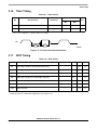
External Clock Operation
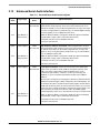
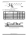
The DSP56367 system clock is an externally supplied square wave voltage source connected to
EXTAL(Figure 3-1).
VIHC
Midpoint
EXTAL
VILC
ETH
ETL
2
4
3
ETC
Note: The midpoint is 0.5 (VIHC + VILC).
Figure 3-1 External Clock Timing
Table 3-5 Clock Operation
No.
1
Characteristics
Symbol
Min
Max
Ef
2.0 ns
150.0
cycle3)
3.11 ns
∞
3)
2.83 ns
157.0 µs
3
3.11 ns
∞
3
2.83 ns
157.0 µs
Frequency of EXTAL (EXTAL Pin Frequency)
The rise and fall time of this external clock should be 2 ns maximum.
2
EXTAL input high1, 2
ETH
• With PLL disabled (46.7%–53.3% duty
• With PLL enabled (42.5%–57.5% duty cycle
3
EXTAL input low1, 2
ETL
• With PLL disabled (46.7%–53.3% duty cycle )
• With PLL enabled (42.5%–57.5% duty cycle )
DSP56367 Technical Data, Rev. 2.1
Freescale Semiconductor
3-5
Phase Lock Loop (PLL) Characteristics
Table 3-5 Clock Operation (continued)
No.
4
7
Characteristics
Symbol
EXTAL cycle time2
Min
Max
ETC
• With PLL disabled
6.7 ns
∞
• With PLL enabled
6.7 ns
273.1 µs
Instruction cycle time = ICYC = TC4
ICYC
• With PLL disabled
13.33 ns
∞
• With PLL enabled
6.67 ns
8.53 µs
1
Measured at 50% of the input transition.
The maximum value for PLL enabled is given for minimum VCO and maximum MF.
3
The indicated duty cycle is for the specified maximum frequency for which a part is rated. The minimum clock high or low time
required for correct operation, however, remains the same at lower operating frequencies; therefore, when a lower clock
frequency is used, the signal symmetry may vary from the specified duty cycle as long as the minimum high time and low time
requirements are met.
4 The maximum value for PLL enabled is given for minimum V
CO and maximum DF.
2
3.8
Phase Lock Loop (PLL) Characteristics
Table 3-6 PLL Characteristics
Characteristics
VCO frequency when PLL enabled (MF × Ef × 2/PDF)
Min
Max
Unit
30
300
MHz
PLL external capacitor (PCAP pin to VCCP) (CPCAP1)
pF
• @ MF ≤ 4
(MF × 580) − 100
(MF × 780) − 140
• @ MF > 4
MF × 830
MF × 1470
1
CPCAP is the value of the PLL capacitor (connected between the PCAP pin and VCCP). The recommended value in pF for
CPCAP can be computed from one of the following equations:
(MF x 680)-120, for MF ≤ 4, or
MF x 1100, for MF > 4.
DSP56367 Technical Data, Rev. 2.1
3-6
Freescale Semiconductor
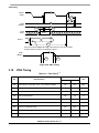
Reset, Stop, Mode Select, and Interrupt Timing
3.9
Reset, Stop, Mode Select, and Interrupt Timing
Table 3-7 Reset, Stop, Mode Select, and Interrupt Timing1
No.
Characteristics
8
Delay from RESET assertion to all pins at reset value2
9
Required RESET duration3
• Power on, external clock generator, PLL disabled
10
11
Expression
Min
Max
Unit
—
—
26.0
ns
50 × ETC
333.4
—
ns
• Power on, external clock generator, PLL enabled
1000 × ETC
6.7
—
µs
• Power on, Internal oscillator
75000 × ETC
500
—
µs
• During STOP, XTAL disabled
75000 × ETC
500
—
µs
• During STOP, XTAL enabled
2.5 × TC
16.7
—
ns
• During normal operation
2.5 × TC
16.7
—
ns
Delay from asynchronous RESET deassertion to first
external address output (internal reset deassertion)4
ns
• Minimum
3.25 × TC + 2.0
23.7
—
• Maximum
20.25 × TC + 10
—
145.0
ns
Syn reset setup time from RESET
• Maximum
12
TC
—
6.7
Syn reset deassert delay time
ns
• Minimum
3.25 × TC + 1.0
22.7
—
• Maximum
20.25 × TC + 5.0
—
140.0
13
Mode select setup time
30.0
—
ns
14
Mode select hold time
0.0
—
ns
15
Minimum edge-triggered interrupt request assertion width
4.4
—
ns
16
Minimum edge-triggered interrupt request deassertion width
4.4
—
ns
17
Delay from IRQA, IRQB, IRQC, IRQD, NMI assertion to
external memory access address out valid
ns
• Caused by first interrupt instruction fetch
4.25 × TC + 2.0
30.3
—
• Caused by first interrupt instruction execution
7.25 × TC + 2.0
50.3
—
18
Delay from IRQA, IRQB, IRQC, IRQD, NMI assertion to
general-purpose transfer output valid caused by first interrupt
instruction execution
10 × TC + 5.0
71.7
—
ns
19
Delay from address output valid caused by first interrupt
instruction execute to interrupt request deassertion for level
sensitive fast interrupts5, 6, 7
(WS + 3.75) × TC – 10.94
—
Note 8
ns
20
Delay from RD assertion to interrupt request deassertion for
level sensitive fast interrupts5, 6, 7
(WS + 3.25) × TC – 10.94
—
Note 8
ns
DSP56367 Technical Data, Rev. 2.1
Freescale Semiconductor
3-7
Reset, Stop, Mode Select, and Interrupt Timing
Table 3-7 Reset, Stop, Mode Select, and Interrupt Timing1 (continued)
No.
Characteristics
21
Delay from WR assertion to interrupt request deassertion for
level sensitive fast interrupts5, 6, 7
Expression
Min
Max
ns
(WS + 3.5) × TC – 10.94
—
Note 8
N/A
—
Note 8
• SRAM WS = 2, 3
1.75 × TC – 4.0
—
Note 8
• SRAM WS ≥ 4
2.75 × TC – 4.0
—
Note 8
22
Synchronous int setup time from IRQs NMI assertion to the
CLKOUT trans.
0.6 × TC – 0.1
3.9
—
23
Synch. int delay time from the CLKOUT trans2 to the first
external address out valid caused by first inst fetch
• DRAM for all WS
• SRAM WS = 1
ns
9.25 × TC + 1.0
62.7
—
• Maximum
24.75 × TC + 5.0
—
170.0
0.6 × TC − 0.1
3.9
—
ns
• PLL is not active during Stop (PCTL Bit 17 = 0) and Stop
delay is enabled (OMR Bit 6 = 0)
PLC × ETC × PDF + (128 K
− PLC/2) × TC
—
—
ms
• PLL is not active during Stop (PCTL Bit 17 = 0) and Stop
delay is not enabled (OMR Bit 6 = 1)
PLC × ETC × PDF + (23.75
+/- 0.5) × TC
—
—
ms
(8.25 ± 0.5) × TC
51.7
58.3
ns
• PLL is not active during Stop (PCTL Bit 17 = 0) and Stop
delay is enabled (OMR Bit 6 = 0)
PLC × ETC × PDF + (128 K
− PLC/2) × TC
—
—
ms
• PLL is not active during Stop (PCTL Bit 17 = 0) and Stop
delay is not enabled (OMR Bit 6 = 1)
PLC × ETC × PDF + (20.5
+/- 0.5) × TC
—
—
ms
5.5 × TC
36.7
—
ns
• HDI08, ESAI, ESAI_1, SHI, DAX, Timer
12TC
—
80.0
• DMA
8TC
—
53.0
• IRQ, NMI (edge trigger)
8TC
—
53.0
• IRQ (level trigger)
12TC
—
80.0
Duration for IRQA assertion to recover from Stop state
25
Delay from IRQA assertion to fetch of first instruction (when
exiting Stop)2, 8
• PLL is active during Stop (PCTL Bit 17 = 1) (Implies No
Stop Delay)
Duration of level sensitive IRQA assertion to ensure interrupt
service (when exiting Stop)2, 8
• PLL is active during Stop (PCTL Bit 17 = 1) (implies no
Stop delay)
27
ns
• Minimum
24
26
Unit
Interrupt Requests Rate
ns
DSP56367 Technical Data, Rev. 2.1
3-8
Freescale Semiconductor
Reset, Stop, Mode Select, and Interrupt Timing
Table 3-7 Reset, Stop, Mode Select, and Interrupt Timing1 (continued)
No.
28
29
1
2
3
4
5
6
7
8
Characteristics
Expression
Min
Max
Unit
ns
DMA Requests Rate
• Data read from HDI08, ESAI, ESAI_1, SHI, DAX
6TC
—
40.0
• Data write to HDI08, ESAI, ESAI_1, SHI, DAX
7TC
—
46.7
• Timer
2TC
• IRQ, NMI (edge trigger)
3TC
—
20.0
4.25 × TC + 2.0
30.3
—
Delay from IRQA, IRQB, IRQC, IRQD, NMI assertion to
external memory (DMA source) access address out valid
13.3
ns
VCCQH = 3.3 V ± 5%; VCC= 1.8V ± 5%; TJ = –40°C to + 95°C, CL = 50 pF
Periodically sampled and not 100% tested.
RESET duration is measured during the time in which RESET is asserted, VCC is valid, and the EXTAL input is active and
valid. When the VCC is valid, but the other “required RESET duration” conditions (as specified above) have not been yet met,
the device circuitry will not be in an initialized state that can result in significant power consumption and heat-up. Designs
should minimize this state to the shortest possible duration.
If PLL does not lose lock.
When using fast interrupts and IRQA, IRQB, IRQC, and IRQD are defined as level-sensitive, timings 19 through 21 apply to
prevent multiple interrupt service. To avoid these timing restrictions, the deasserted Edge-triggered mode is recommended
when using fast interrupts. Long interrupts are recommended when using Level-sensitive mode.
WS = number of wait states (measured in clock cycles, number of TC).
Use expression to compute maximum value.
This timing depends on several settings:
For PLL disable, using external clock (PCTL Bit 16 = 1), no stabilization delay is required and recovery time will be defined
by the PCTL Bit 17 and OMR Bit 6 settings.
For PLL enable, if PCTL Bit 17 is 0, the PLL is shutdown during Stop. Recovering from Stop requires the PLL to get locked.
The PLL lock procedure duration, PLL Lock Cycles (PLC), may be in the range of 0 to 1000 cycles. This procedure occurs
in parallel with the stop delay counter, and stop recovery will end when the last of these two events occurs: the stop delay
counter completes count or PLL lock procedure completion.
PLC value for PLL disable is 0.
The maximum value for ETC is 4096 (maximum MF) divided by the desired internal frequency (i.e., for 150 MHz it is
4096/150 MHz = 27.3 µs). During the stabilization period, TC, TH, and TL will not be constant, and their width may vary, so
timing may vary as well.
DSP56367 Technical Data, Rev. 2.1
Freescale Semiconductor
3-9
Reset, Stop, Mode Select, and Interrupt Timing
VIH
RESET
9
10
8
All Pins
Reset Value
First Fetch
A0–A17
AA0460
Figure 3-2 Reset Timing
First Interrupt Instruction
Execution/Fetch
A0–A17
RD
20
WR
21
IRQA, IRQB,
17
19
IRQC, IRQD,
NMI
a) First Interrupt Instruction Execution
General
Purpose
I/O
18
IRQA, IRQB,
IRQC, IRQD,
NMI
b) General Purpose I/O
Figure 3-3 External Fast Interrupt Timing
DSP56367 Technical Data, Rev. 2.1
3-10
Freescale Semiconductor
Reset, Stop, Mode Select, and Interrupt Timing
IRQA, IRQB,
IRQC, IRQD,
NMI
15
IRQA, IRQB,
IRQC, IRQD,
NMI
16
AA0463
Figure 3-4 External Interrupt Timing (Negative Edge-Triggered)
VIH
RESET
13
14
VIH
MODA, MODB,
MODC, MODD,
PINIT
VIH
VIL
VIL
IRQA, IRQB,
IRQD, NMI
AA0465
Figure 3-5 Operating Mode Select Timing
24
IRQA
25
First Instruction Fetch
A0–A17
AA0466
Figure 3-6 Recovery from Stop State Using IRQA Interrupt Service
DSP56367 Technical Data, Rev. 2.1
Freescale Semiconductor
3-11
External Memory Expansion Port (Port A)
26
IRQA
25
A0–A17
First IRQA Interrupt Instruction Fetch
AA0467
Figure 3-7 Recovery from Stop State Using IRQA Interrupt Service
DMA Source Address
A0–A17
RD
WR
29
IRQA, IRQB,
First Interrupt Instruction Execution
IRQC, IRQD,
AA1104
NMI
Figure 3-8 External Memory Access (DMA Source) Timing
3.10
External Memory Expansion Port (Port A)
3.10.1
SRAM Timing
Table 3-8 SRAM Read and Write Accesses
No.
100
101
102
103
Characteristics
Symbol
Address valid and AA assertion pulse width
Address and AA valid to WR assertion
WR assertion pulse width
WR deassertion to address not valid
Expression1
tRC, tWC (WS + 2) × TC − 4.0 [2 ≤ WS ≤ 7]
tAS
tWP
tWR
150 MHz
Unit
Min
Max
22.7
—
ns
(WS + 3) × TC − 4.0 [WS ≥ 8]
69.3
—
ns
0.75 × TC − 2.0[2 ≤ WS ≤ 3]
3.0
—
ns
1.25 × TC − 2.0[WS ≥ 4]
6.3
—
ns
WS × TC − 4.0 [2 ≤ WS ≤ 3]
9.3
—
ns
(WS − 0.5) × TC − 4.0[WS ≥ 4]
19.3
—
ns
1.25 × TC − 4.0[2 ≤ WS ≤ 7]
4.3
—
ns
2.25 × TC − 4.0[WS ≥ 8]
11.0
—
ns
DSP56367 Technical Data, Rev. 2.1
3-12
Freescale Semiconductor
External Memory Expansion Port (Port A)
Table 3-8 SRAM Read and Write Accesses (continued)
No.
Characteristics
Symbol
Expression1
150 MHz
Unit
Min
Max
tAA, tAC
(WS + 0.75) × TC − 5.0 [WS ≥ 2]
—
13.3
ns
RD assertion to input data valid
tOE
(WS + 0.25) × TC − 5.0 [WS ≥ 2]
—
10.0
ns
106
RD deassertion to data not valid (data hold time)
tOHZ
0.0
—
ns
107
Address valid to WR deassertion2
tAW
(WS + 0.75) × TC − 4.0 [WS ≥ 2]
14.3
—
ns
108
Data valid to WR deassertion (data setup time)
tDS (tDW) (WS − 0.25) × TC − 3.0 [WS ≥ 2]
8.7
—
ns
109
Data hold time from WR deassertion
1.25 × TC − 2.0[2 ≤ WS ≤ 7]
6.3
—
ns
2.25 × TC − 2.0 [WS ≥ 8]
13.0
—
ns
0.25 × TC − 3.7 [2 ≤ WS ≤ 3]
-2.0
—
ns
−0.25 × TC − 3.7 [WS ≥ 4]
-5.4
—
ns
0.25 × TC + 0.2 [2 ≤ WS ≤ 3]
—
1.9
ns
1.25 × TC + 0.2 [4 ≤ WS ≤ 7]
—
8.5
ns
2.25 × TC + 0.2 [WS ≥ 8]
—
15.2
ns
1.25 × TC − 4.0 [2 ≤ WS ≤ 3]
4.3
—
ns
2.25 × TC − 4.0 [4 ≤ WS ≤ 7]
11.0
—
ns
3.25 × TC − 4.0 [WS ≥ 8]
17.7
—
ns
1.75 × TC − 4.0 [2 ≤ WS ≤ 7]
7.7
—
ns
2.75 × TC − 4.0 [WS ≥ 8]
14.3
—
ns
2.0 × TC − 4.0 [2 ≤ WS ≤ 3]
9.3
—
ns
2.5 × TC − 4.0 [4 ≤ WS ≤ 7]
12.7
—
ns
3.5 × TC − 4.0 [WS ≥ 8]
19.3
—
ns
0.5 × TC − 2.0
1.3
—
ns
(WS + 0.25) × TC −4.0
11.0
—
ns
1.25 × TC − 2.0 [2 ≤ WS ≤ 7]
6.3
—
ns
2.25 × TC − 2.0 [WS ≥ 8]
13.0
—
ns
0.25 × TC + 2.0
3.7
—
ns
0.0
—
ns
104
Address and AA valid to input data valid
105
110
111
112
113
114
WR assertion to data active
—
WR deassertion to data high impedance
Previous RD deassertion to data active (write)
RD deassertion time
WR deassertion time
115
Address valid to RD assertion
116
RD assertion pulse width
117
RD deassertion to address not valid
tDH
118
TA setup before RD or WR deassertion3
119
TA hold after RD or WR deassertion
—
—
1
WS is the number of wait states specified in the BCR. The value is given for the minimum for a given category. (For example,
for a category of [2 ≤ WS ≤ 7] timing is specified for 2 wait states.) Two wait states is the minimum otherwise.
2 Timings 100, 107 are guaranteed by design, not tested.
3 In the case of TA negation: timing 118 is relative to the deassertion edge of RD or WR were TA to remain active.
DSP56367 Technical Data, Rev. 2.1
Freescale Semiconductor
3-13
External Memory Expansion Port (Port A)
100
A0–A17
AA0–AA2
113
117
116
RD
115
105
106
WR
104
119
118
TA
Data
In
D0–D23
AA0468
Figure 3-9 SRAM Read Access
100
A0–A17
AA0–AA2
107
101
102
103
WR
114
RD
119
118
TA
108
109
Data
Out
D0–D23
Figure 3-10 SRAM Write Access
DSP56367 Technical Data, Rev. 2.1
3-14
Freescale Semiconductor
External Memory Expansion Port (Port A)
3.10.2
DRAM Timing
The selection guides provided in Figure 3-11 and Figure 3-14 should be used for primary selection only.
Final selection should be based on the timing provided in the following tables. As an example, the selection
guide suggests that 4 wait states must be used for 100 MHz operation when using Page Mode DRAM.
However, by using the information in the appropriate table, a designer may choose to evaluate whether
fewer wait states might be used by determining which timing prevents operation at 100 MHz, running the
chip at a slightly lower frequency (e.g., 95 MHz), using faster DRAM (if it becomes available), and control
factors such as capacitive and resistive load to improve overall system performance.
Note: This figure should be use for primary selection. For
exact and detailed timings see the following tables.
DRAM Type
(tRAC ns)
100
80
70
60
Chip Frequency
50
40
66
80
100
120
(MHz)
1 Wait States
3 Wait States
2 Wait States
4 Wait States
AA0472
Figure 3-11 DRAM Page Mode Wait States Selection Guide
DSP56367 Technical Data, Rev. 2.1
Freescale Semiconductor
3-15
External Memory Expansion Port (Port A)
Table 3-9 DRAM Page Mode Timings, Three Wait States1, 2, 3
100 MHz
No.
131
Characteristics
Page mode cycle time for two consecutive accesses of the same
direction
Symbol
tPC
Page mode cycle time for mixed (read and write) accesses
Expression4
Unit
Min
Max
2 × TC
20.0
—
1.25 × TC
12.5
—
ns
132
CAS assertion to data valid (read)
tCAC
2 × TC − 7.0
—
13.0
ns
133
Column address valid to data valid (read)
tAA
3 × TC − 7.0
—
23.0
ns
134
CAS deassertion to data not valid (read hold time)
tOFF
0.0
—
ns
135
Last CAS assertion to RAS deassertion
tRSH
2.5 × TC − 4.0
21.0
—
ns
136
Previous CAS deassertion to RAS deassertion
tRHCP
4.5 × TC − 4.0
41.0
—
ns
137
CAS assertion pulse width
tCAS
2 × TC − 4.0
16.0
—
ns
138
Last CAS deassertion to RAS assertion5
tCRP
ns
• BRW[1:0] = 00, 01— not applicable
• BRW[1:0] = 10
4.75 × TC − 6.0
41.5
—
• BRW[1:0] = 11
6.75 × TC − 6.0
61.5
—
139
CAS deassertion pulse width
tCP
1.5 × TC − 4.0
11.0
—
ns
140
Column address valid to CAS assertion
tASC
TC − 4.0
6.0
—
ns
141
CAS assertion to column address not valid
tCAH
2.5 × TC − 4.0
21.0
—
ns
142
Last column address valid to RAS deassertion
tRAL
4 × TC − 4.0
36.0
—
ns
143
WR deassertion to CAS assertion
tRCS
1.25 × TC − 4.0
8.5
—
ns
144
CAS deassertion to WR assertion
tRCH
0.75 × TC − 4.0
3.5
—
ns
145
CAS assertion to WR deassertion
tWCH
2.25 × TC − 4.2
18.3
—
ns
146
WR assertion pulse width
tWP
3.5 × TC − 4.5
30.5
—
ns
147
Last WR assertion to RAS deassertion
tRWL
3.75 × TC − 4.3
33.2
—
ns
148
WR assertion to CAS deassertion
tCWL
3.25 × TC − 4.3
28.2
—
ns
149
Data valid to CAS assertion (write)
tDS
0.5 × TC − 4.0
1.0
—
ns
150
CAS assertion to data not valid (write)
tDH
2.5 × TC − 4.0
21.0
—
ns
151
WR assertion to CAS assertion
tWCS
1.25 × TC − 4.3
8.2
—
ns
152
Last RD assertion to RAS deassertion
tROH
3.5 × TC − 4.0
31.0
—
ns
DSP56367 Technical Data, Rev. 2.1
3-16
Freescale Semiconductor
External Memory Expansion Port (Port A)
Table 3-9 DRAM Page Mode Timings, Three Wait States1, 2, 3 (continued)
100 MHz
No.
1
2
3
4
5
6
Characteristics
Symbol
153
RD assertion to data valid
tGA
154
RD deassertion to data not valid6
tGZ
155
WR assertion to data active
156
WR deassertion to data high impedance
Expression4
Unit
Min
Max
—
18.0
ns
0.0
—
ns
0.75 × TC − 0.3
7.2
—
ns
0.25 × TC
—
2.5
ns
2.5 × TC − 7.0
The number of wait states for Page mode access is specified in the DCR.
The refresh period is specified in the DCR.
The asynchronous delays specified in the expressions are valid for DSP56367.
All the timings are calculated for the worst case. Some of the timings are better for specific cases (e.g., tPC equals 4 × TC for
read-after-read or write-after-write sequences).
BRW[1:0] (DRAM control register bits) defines the number of wait states that should be inserted in each DRAM out-of
page-access.
RD deassertion will always occur after CAS deassertion; therefore, the restricted timing is tOFF and not tGZ.
Table 3-10 DRAM Page Mode Timings, Four Wait States1, 2, 3
100 MHz
No.
131
Characteristics
Page mode cycle time for two consecutive accesses of the
same direction
Symbol
tPC
Page mode cycle time for mixed (read and write) accesses
Expression4
Unit
Min
Max
5 × TC
50.0
—
4.5 × TC
45.0
—
ns
132
CAS assertion to data valid (read)
tCAC
2.75 × TC − 5.7
—
21.8
ns
133
Column address valid to data valid (read)
tAA
3.75 × TC − 5.7
—
31.8
ns
134
CAS deassertion to data not valid (read hold time)
tOFF
0.0
—
ns
135
Last CAS assertion to RAS deassertion
tRSH
3.5 × TC − 4.0
31.0
—
ns
136
Previous CAS deassertion to RAS deassertion
tRHCP
6 × TC − 4.0
56.0
—
ns
137
CAS assertion pulse width
tCAS
2.5 × TC − 4.0
21.0
—
ns
138
Last CAS deassertion to RAS assertion5
tCRP
—
—
—
—
• BRW[1–0] = 10
5.25 × TC − 6.0
46.5
—
ns
• BRW[1–0] = 11
7.25 × TC − 6.0
66.5
—
ns
• BRW[1–0] = 00, 01—Not applicable
139
CAS deassertion pulse width
tCP
2 × TC − 4.0
16.0
—
ns
140
Column address valid to CAS assertion
tASC
TC − 4.0
6.0
—
ns
DSP56367 Technical Data, Rev. 2.1
Freescale Semiconductor
3-17
External Memory Expansion Port (Port A)
Table 3-10 DRAM Page Mode Timings, Four Wait States1, 2, 3 (continued)
100 MHz
No.
1
2
3
4
5
6
Characteristics
Symbol
Expression4
Unit
Min
Max
141
CAS assertion to column address not valid
tCAH
3.5 × TC − 4.0
31.0
—
ns
142
Last column address valid to RAS deassertion
tRAL
5 × TC − 4.0
46.0
—
ns
143
WR deassertion to CAS assertion
tRCS
1.25 × TC − 4.0
8.5
—
ns
144
CAS deassertion to WR assertion
tRCH
1.25 × TC – 3.7
8.8
—
ns
145
CAS assertion to WR deassertion
tWCH
3.25 × TC − 4.2
28.3
—
ns
146
WR assertion pulse width
tWP
4.5 × TC − 4.5
40.5
—
ns
147
Last WR assertion to RAS deassertion
tRWL
4.75 × TC − 4.3
43.2
—
ns
148
WR assertion to CAS deassertion
tCWL
3.75 × TC − 4.3
33.2
—
ns
149
Data valid to CAS assertion (write)
tDS
0.5 × TC – 4.5
0.5
—
ns
150
CAS assertion to data not valid (write)
tDH
3.5 × TC − 4.0
31.0
—
ns
151
WR assertion to CAS assertion
tWCS
1.25 × TC − 4.3
8.2
—
ns
152
Last RD assertion to RAS deassertion
tROH
4.5 × TC − 4.0
41.0
—
ns
153
RD assertion to data valid
tGA
3.25 × TC − 5.7
—
26.8
ns
154
RD deassertion to data not valid6
tGZ
0.0
—
ns
155
WR assertion to data active
0.75 × TC – 1.5
6.0
—
ns
156
WR deassertion to data high impedance
0.25 × TC
—
2.5
ns
The number of wait states for Page mode access is specified in the DCR.
The refresh period is specified in the DCR.
The asynchronous delays specified in the expressions are valid for DSP56367.
All the timings are calculated for the worst case. Some of the timings are better for specific cases (for example, tPC equals
3 × TC for read-after-read or write-after-write sequences). An expressions is used to calculate the maximum or minimum
value listed, as appropriate.
BRW[1–0] (DRAM control register bits) defines the number of wait states that should be inserted in each DRAM out-of-page
access.
RD deassertion always occurs after CAS deassertion; therefore, the restricted timing is tOFF and not tGZ.
DSP56367 Technical Data, Rev. 2.1
3-18
Freescale Semiconductor
External Memory Expansion Port (Port A)
RAS
136
131
135
CAS
137
139
138
140
141
A0–A17
Row
Add
142
Column
Address
Column
Address
151
Last Column
Address
144
143
145
147
WR
146
148
RD
155
156
150
149
D0–D23
Data Out
Data Out
Data Out
AA0473
Figure 3-12 DRAM Page Mode Write Accesses
DSP56367 Technical Data, Rev. 2.1
Freescale Semiconductor
3-19
External Memory Expansion Port (Port A)
RAS
136
131
135
CAS
137
139
140
A0–A17
Row
Add
Column
Address
138
141
142
Last Column
Address
Column
Address
143
WR
132
133
152
153
RD
134
154
D0–D23
Data In
Data In
Data In
AA0474
Figure 3-13 DRAM Page Mode Read Accesses
DSP56367 Technical Data, Rev. 2.1
3-20
Freescale Semiconductor
External Memory Expansion Port (Port A)
DRAM Type
(tRAC ns)
Note: This figure should be use for primary selection. For exact
and detailed timings see the following tables.
100
80
70
60
50
40
66
80
120
100
4 Wait States
11 Wait States
8 Wait States
15 Wait States
Chip Frequency
(MHz)
AA0475
Figure 3-14 DRAM Out-of-Page Wait States Selection Guide
Table 3-11 DRAM Out-of-Page and Refresh Timings, Four Wait States1, 2
20 MHz3
No.
Characteristics
Symbol
30 MHz3
Expression
Unit
Min
Max
Min
Max
157
Random read or write cycle time
tRC
5 × TC
250.0
—
166.7
—
ns
158
RAS assertion to data valid (read)
tRAC
2.75 × TC − 7.5
—
130.0
—
84.2
ns
159
CAS assertion to data valid (read)
tCAC
1.25 × TC − 7.5
—
55.0
—
34.2
ns
160
Column address valid to data valid (read)
tAA
1.5 × TC − 7.5
—
67.5
—
42.5
ns
161
CAS deassertion to data not valid (read hold
time)
tOFF
0.0
—
0.0
—
ns
162
RAS deassertion to RAS assertion
tRP
1.75 × TC − 4.0
83.5
—
54.3
—
ns
163
RAS assertion pulse width
tRAS
3.25 × TC − 4.0
158.5
—
104.3
—
ns
164
CAS assertion to RAS deassertion
tRSH
1.75 × TC − 4.0
83.5
—
54.3
—
ns
DSP56367 Technical Data, Rev. 2.1
Freescale Semiconductor
3-21
External Memory Expansion Port (Port A)
Table 3-11 DRAM Out-of-Page and Refresh Timings, Four Wait States1, 2 (continued)
20 MHz3
No.
Characteristics
Symbol
30 MHz3
Expression
Unit
Min
Max
Min
Max
165
RAS assertion to CAS deassertion
tCSH
2.75 × TC − 4.0
133.5
—
87.7
—
ns
166
CAS assertion pulse width
tCAS
1.25 × TC − 4.0
58.5
—
37.7
—
ns
167
RAS assertion to CAS assertion
tRCD
1.5 × TC ± 2
73.0
77.0
48.0
52.0
ns
168
RAS assertion to column address valid
tRAD
1.25 × TC ± 2
60.5
64.5
39.7
43.7
ns
169
CAS deassertion to RAS assertion
tCRP
2.25 × TC − 4.0
108.5
—
71.0
—
ns
170
CAS deassertion pulse width
tCP
1.75 × TC − 4.0
83.5
—
54.3
—
ns
171
Row address valid to RAS assertion
tASR
1.75 × TC − 4.0
83.5
—
54.3
—
ns
172
RAS assertion to row address not valid
tRAH
1.25 × TC − 4.0
58.5
—
37.7
—
ns
173
Column address valid to CAS assertion
tASC
0.25 × TC − 4.0
8.5
—
4.3
—
ns
174
CAS assertion to column address not valid
tCAH
1.75 × TC − 4.0
83.5
—
54.3
—
ns
175
RAS assertion to column address not valid
tAR
3.25 × TC − 4.0
158.5
—
104.3
—
ns
176
Column address valid to RAS deassertion
tRAL
2 × TC − 4.0
96.0
—
62.7
—
ns
177
WR deassertion to CAS assertion
tRCS
1.5 × TC − 3.8
71.2
—
46.2
—
ns
178
CAS deassertion to WR assertion
tRCH
0.75 × TC − 3.7
33.8
—
21.3
—
ns
179
RAS deassertion to WR assertion
tRRH
0.25 × TC − 3.7
8.8
—
4.6
—
ns
180
CAS assertion to WR deassertion
tWCH
1.5 × TC − 4.2
70.8
—
45.8
—
ns
181
RAS assertion to WR deassertion
tWCR
3 × TC − 4.2
145.8
—
95.8
—
ns
182
WR assertion pulse width
tWP
4.5 × TC − 4.5
220.5
—
145.5
—
ns
183
WR assertion to RAS deassertion
tRWL
4.75 × TC − 4.3
233.2
—
154.0
—
ns
184
WR assertion to CAS deassertion
tCWL
4.25 × TC − 4.3
208.2
—
137.4
—
ns
185
Data valid to CAS assertion (write)
tDS
2.25 × TC − 4.0
108.5
—
71.0
—
ns
186
CAS assertion to data not valid (write)
tDH
1.75 × TC − 4.0
83.5
—
54.3
—
ns
187
RAS assertion to data not valid (write)
tDHR
3.25 × TC − 4.0
158.5
—
104.3
—
ns
188
WR assertion to CAS assertion
tWCS
3 × TC − 4.3
145.7
—
95.7
—
ns
189
CAS assertion to RAS assertion (refresh)
tCSR
0.5 × TC − 4.0
21.0
—
12.7
—
ns
190
RAS deassertion to CAS assertion (refresh)
tRPC
1.25 × TC − 4.0
58.5
—
37.7
—
ns
DSP56367 Technical Data, Rev. 2.1
3-22
Freescale Semiconductor
External Memory Expansion Port (Port A)
Table 3-11 DRAM Out-of-Page and Refresh Timings, Four Wait States1, 2 (continued)
20 MHz3
No.
Characteristics
Symbol
30 MHz3
Expression
Unit
Min
Max
Min
Max
191
RD assertion to RAS deassertion
tROH
4.5 × TC − 4.0
221.0
—
146.0
—
ns
192
RD assertion to data valid
tGA
4 × TC − 7.5
—
192.5
—
125.8
ns
193
RD deassertion to data not valid4
tGZ
0.0
—
0.0
—
ns
194
WR assertion to data active
0.75 × TC − 0.3
37.2
—
24.7
—
ns
195
WR deassertion to data high impedance
0.25 × TC
—
12.5
—
8.3
ns
1
The number of wait states for out of page access is specified in the DCR.
The refresh period is specified in the DCR.
3 Reduced DSP clock speed allows use of DRAM out-of-page access with four Wait states (Figure 3-14).
4 RD deassertion will always occur after CAS deassertion; therefore, the restricted timing is t
OFF and not tGZ.
2
Table 3-12 DRAM Out-of-Page and Refresh Timings, Eleven Wait States1, 2, 3
100 MHz
No.
Characteristics
Symbol
Expression
Unit
Min
Max
157
Random read or write cycle time
tRC
12 × TC
120.0
—
ns
158
RAS assertion to data valid (read)
tRAC
6.25 × TC − 7.0
—
55.5
ns
159
CAS assertion to data valid (read)
tCAC
3.75 × TC − 7.0
—
30.5
ns
160
Column address valid to data valid (read)
tAA
4.5 × TC − 7.0
—
38.0
ns
161
CAS deassertion to data not valid (read hold time)
tOFF
0.0
—
ns
162
RAS deassertion to RAS assertion
tRP
4.25 × TC − 4.0
38.5
—
ns
163
RAS assertion pulse width
tRAS
7.75 × TC − 4.0
73.5
—
ns
164
CAS assertion to RAS deassertion
tRSH
5.25 × TC − 4.0
48.5
—
ns
165
RAS assertion to CAS deassertion
tCSH
6.25 × TC − 4.0
58.5
—
ns
166
CAS assertion pulse width
tCAS
3.75 × TC − 4.0
33.5
—
ns
167
RAS assertion to CAS assertion
tRCD
2.5 × TC ± 4.0
21.0
29.0
ns
168
RAS assertion to column address valid
tRAD
1.75 × TC ± 4.0
13.5
21.5
ns
169
CAS deassertion to RAS assertion
tCRP
5.75 × TC − 4.0
53.5
—
ns
170
CAS deassertion pulse width
tCP
4.25 × TC − 4.0
38.5
—
ns
171
Row address valid to RAS assertion
tASR
4.25 × TC − 4.0
38.5
—
ns
172
RAS assertion to row address not valid
tRAH
1.75 × TC − 4.0
13.5
—
ns
DSP56367 Technical Data, Rev. 2.1
Freescale Semiconductor
3-23
External Memory Expansion Port (Port A)
Table 3-12 DRAM Out-of-Page and Refresh Timings, Eleven Wait States1, 2, 3 (continued)
100 MHz
No.
Characteristics
Symbol
Expression
Unit
Min
Max
173
Column address valid to CAS assertion
tASC
0.75 × TC − 4.0
3.5
—
ns
174
CAS assertion to column address not valid
tCAH
5.25 × TC − 4.0
48.5
—
ns
175
RAS assertion to column address not valid
tAR
7.75 × TC − 4.0
73.5
—
ns
176
Column address valid to RAS deassertion
tRAL
6 × TC − 4.0
56.0
—
ns
177
WR deassertion to CAS assertion
tRCS
3.0 × TC − 4.0
26.0
—
ns
178
CAS deassertion to WR4 assertion
tRCH
1.75 × TC − 4.0
13.5
—
ns
179
RAS deassertion to WR4 assertion
tRRH
0.25 × TC − 2.0
0.5
—
ns
180
CAS assertion to WR deassertion
tWCH
5 × TC − 4.2
45.8
—
ns
181
RAS assertion to WR deassertion
tWCR
7.5 × TC − 4.2
70.8
—
ns
182
WR assertion pulse width
tWP
11.5 × TC − 4.5
110.5
—
ns
183
WR assertion to RAS deassertion
tRWL
11.75 × TC − 4.3
113.2
—
ns
184
WR assertion to CAS deassertion
tCWL
10.25 × TC − 4.3
103.2
—
ns
185
Data valid to CAS assertion (write)
tDS
5.75 × TC − 4.0
53.5
—
ns
186
CAS assertion to data not valid (write)
tDH
5.25 × TC − 4.0
48.5
—
ns
187
RAS assertion to data not valid (write)
tDHR
7.75 × TC − 4.0
73.5
—
ns
188
WR assertion to CAS assertion
tWCS
6.5 × TC − 4.3
60.7
—
ns
189
CAS assertion to RAS assertion (refresh)
tCSR
1.5 × TC − 4.0
11.0
—
ns
190
RAS deassertion to CAS assertion (refresh)
tRPC
2.75 × TC − 4.0
23.5
—
ns
191
RD assertion to RAS deassertion
tROH
11.5 × TC − 4.0
111.0
—
ns
192
RD assertion to data valid
tGA
10 × TC − 7.0
—
93.0
ns
193
RD deassertion to data not valid5
tGZ
0.0
—
ns
194
WR assertion to data active
0.75 × TC − 0.3
7.2
—
ns
195
WR deassertion to data high impedance
0.25 × TC
—
2.5
ns
1
The number of wait states for out-of-page access is specified in the DCR.
The refresh period is specified in the DCR.
3 The asynchronous delays specified in the expressions are valid for DSP56367.
4 Either t
RCH or tRRH must be satisfied for read cycles.
5 RD deassertion will always occur after CAS deassertion; therefore, the restricted timing is t
OFF and not tGZ.
2
DSP56367 Technical Data, Rev. 2.1
3-24
Freescale Semiconductor
External Memory Expansion Port (Port A)
Table 3-13 DRAM Out-of-Page and Refresh Timings, Fifteen Wait States1, 2
100 MHz
No.
Characteristics
Symbol
Expression3
Unit
Min
Max
157
Random read or write cycle time
tRC
16 × TC
160.0
—
ns
158
RAS assertion to data valid (read)
tRAC
8.25 × TC − 5.7
—
76.8
ns
159
CAS assertion to data valid (read)
tCAC
4.75 × TC − 5.7
—
41.8
ns
160
Column address valid to data valid (read)
tAA
5.5 × TC − 5.7
—
49.3
ns
161
CAS deassertion to data not valid (read hold time)
tOFF
0.0
0.0
—
ns
162
RAS deassertion to RAS assertion
tRP
6.25 × TC − 4.0
58.5
—
ns
163
RAS assertion pulse width
tRAS
9.75 × TC − 4.0
93.5
—
ns
164
CAS assertion to RAS deassertion
tRSH
6.25 × TC − 4.0
58.5
—
ns
165
RAS assertion to CAS deassertion
tCSH
8.25 × TC − 4.0
78.5
—
ns
166
CAS assertion pulse width
tCAS
4.75 × TC − 4.0
43.5
—
ns
167
RAS assertion to CAS assertion
tRCD
3.5 × TC ± 2
33.0
37.0
ns
168
RAS assertion to column address valid
tRAD
2.75 × TC ± 2
25.5
29.5
ns
169
CAS deassertion to RAS assertion
tCRP
7.75 × TC − 4.0
73.5
—
ns
170
CAS deassertion pulse width
tCP
6.25 × TC – 6.0
56.5
—
ns
171
Row address valid to RAS assertion
tASR
6.25 × TC − 4.0
58.5
—
ns
172
RAS assertion to row address not valid
tRAH
2.75 × TC − 4.0
23.5
—
ns
173
Column address valid to CAS assertion
tASC
0.75 × TC − 4.0
3.5
—
ns
174
CAS assertion to column address not valid
tCAH
6.25 × TC − 4.0
58.5
—
ns
175
RAS assertion to column address not valid
tAR
9.75 × TC − 4.0
93.5
—
ns
176
Column address valid to RAS deassertion
tRAL
7 × TC − 4.0
66.0
—
ns
177
WR deassertion to CAS assertion
tRCS
5 × TC − 3.8
46.2
—
ns
178
CAS deassertion to WR4 assertion
tRCH
1.75 × TC – 3.7
13.8
—
ns
179
RAS deassertion to WR4 assertion
tRRH
0.25 × TC − 2.0
0.5
—
ns
180
CAS assertion to WR deassertion
tWCH
6 × TC − 4.2
55.8
—
ns
181
RAS assertion to WR deassertion
tWCR
9.5 × TC − 4.2
90.8
—
ns
182
WR assertion pulse width
tWP
15.5 × TC − 4.5
150.5
—
ns
DSP56367 Technical Data, Rev. 2.1
Freescale Semiconductor
3-25
External Memory Expansion Port (Port A)
Table 3-13 DRAM Out-of-Page and Refresh Timings, Fifteen Wait States1, 2 (continued)
100 MHz
No.
Characteristics
Symbol
Expression3
Unit
Min
Max
183
WR assertion to RAS deassertion
tRWL
15.75 × TC − 4.3
153.2
—
ns
184
WR assertion to CAS deassertion
tCWL
14.25 × TC − 4.3
138.2
—
ns
185
Data valid to CAS assertion (write)
tDS
8.75 × TC − 4.0
83.5
—
ns
186
CAS assertion to data not valid (write)
tDH
6.25 × TC − 4.0
58.5
—
ns
187
RAS assertion to data not valid (write)
tDHR
9.75 × TC − 4.0
93.5
—
ns
188
WR assertion to CAS assertion
tWCS
9.5 × TC − 4.3
90.7
—
ns
189
CAS assertion to RAS assertion (refresh)
tCSR
1.5 × TC − 4.0
11.0
—
ns
190
RAS deassertion to CAS assertion (refresh)
tRPC
4.75 × TC − 4.0
43.5
—
ns
191
RD assertion to RAS deassertion
tROH
15.5 × TC − 4.0
151.0
—
ns
192
RD assertion to data valid
tGA
14 × TC − 5.7
—
134.3
ns
193
RD deassertion to data not valid5
tGZ
0.0
—
ns
194
WR assertion to data active
0.75 × TC – 1.5
6.0
—
ns
195
WR deassertion to data high impedance
0.25 × TC
—
2.5
ns
1
The number of wait states for an out-of-page access is specified in the DCR.
The refresh period is specified in the DCR.
3 An expression is used to compute the maximum or minimum value listed (or both if the expression includes ±).
4 Either t
RCH or tRRH must be satisfied for read cycles.
5 RD deassertion always occurs after CAS deassertion; therefore, the restricted timing is t
OFF and not tGZ.
2
DSP56367 Technical Data, Rev. 2.1
3-26
Freescale Semiconductor
External Memory Expansion Port (Port A)
157
163
162
162
165
RAS
167
164
169
168
170
166
CAS
171
173
174
175
A0–A17
Row Address
Column Address
172
176
177
179
191
WR
168
160
159
RD
193
158
192
D0–D23
161
Data
In
AA0476
Figure 3-15 DRAM Out-of-Page Read Access
DSP56367 Technical Data, Rev. 2.1
Freescale Semiconductor
3-27
External Memory Expansion Port (Port A)
157
162
163
162
165
RAS
167
164
169
168
166
170
CAS
171
173
172
174
176
A0–A17
Row Address
Column Address
181
175
188
180
182
WR
184
183
RD
187
186
185
195
194
D0–D23
Data Out
AA0477
Figure 3-16 DRAM Out-of-Page Write Access
DSP56367 Technical Data, Rev. 2.1
3-28
Freescale Semiconductor
External Memory Expansion Port (Port A)
157
163
162
162
RAS
190
170
165
CAS
189
177
WR
AA0478
Figure 3-17 DRAM Refresh Access
3.10.3
Arbitration Timings
Table 3-14 Asynchronous Bus Arbitration Timing1, 2, 3
150 MHz
No.
Characteristics
250
BB assertion window from BG input negation.
251
Delay from BB assertion to BG assertion
Expression
Unit
Min
Max
2 .5* Tc + 5
—
21.7
ns
2 * Tc + 5
18.3
—
ns
1
Bit 13 in the OMR register must be set to enter Asynchronous Arbitration mode.
If Asynchronous Arbitration mode is active, none of the timings in Table 3-14 is required.
3 In order to guarantee timings 250, and 251, it is recommended to assert BG inputs to different 56300 devices (on the same
bus) in a non overlap manner as shown in Figure 3-18.
2
DSP56367 Technical Data, Rev. 2.1
Freescale Semiconductor
3-29
External Memory Expansion Port (Port A)
BG1
BB
250
BG2
251
Figure 3-18 Asynchronous Bus Arbitration Timing
BG1
BG2
250+251
Figure 3-19 Asynchronous Bus Arbitration Timing
3.10.4
Background explanation for Asynchronous Bus Arbitration:
The asynchronous bus arbitration is enabled by internal synchronization circuits on BG and BB inputs.
These synchronization circuits add delay from the external signal until it is exposed to internal logic. As a
result of this delay, a 56300 part may assume mastership and assert BB for some time after BG is negated.
This is the reason for timing 250.
Once BB is asserted, there is a synchronization delay from BB assertion to the time this assertion is
exposed to other 56300 components which are potential masters on the same bus. If BG input is asserted
before that time, a situation of BG asserted, and BB negated, may cause another 56300 component to
assume mastership at the same time. Therefore some non-overlap period between one BG input active to
another BG input active is required. Timing 251 ensures that such a situation is avoided.
DSP56367 Technical Data, Rev. 2.1
3-30
Freescale Semiconductor
Parallel Host Interface (HDI08) Timing
3.11
Parallel Host Interface (HDI08) Timing
Table 3-15 Host Interface (HDI08) Timing1, 2, 3
150 MHz
No.
317
Characteristics
Read data strobe assertion width4
Expression
Unit
Min
Max
TC + 9.9
16.7
—
ns
—
9.9
—
ns
2.5 × TC + 6.6
23.3
—
ns
—
13.2
—
ns
HACK read assertion width
318
Read data strobe deassertion width4
HACK read deassertion width
319
Read data strobe deassertion width4 after “Last Data Register” reads5, 6, or
between two consecutive CVR, ICR, or ISR reads7
HACK deassertion width after “Last Data Register” reads5, 6
320
Write data strobe assertion width8
HACK write assertion width
321
Write data strobe deassertion width8
ns
HACK write deassertion width
• after ICR, CVR and “Last Data Register” writes5
2.5 × TC + 6.6
• after IVR writes, or
23.3
—
16.5
—
• after TXH:TXM writes (with HBE=0), or
• after TXL:TXM writes (with HBE=1)
322
HAS assertion width
—
9.9
—
ns
323
HAS deassertion to data strobe assertion9
—
0.0
—
ns
324
Host data input setup time before write data strobe deassertion8
—
9.9
—
ns
—
3.3
—
ns
—
3.3
—
ns
—
—
24.2
ns
—
—
9.9
ns
—
3.3
—
ns
Host data input setup time before HACK write deassertion
325
Host data input hold time after write data strobe deassertion8
Host data input hold time after HACK write deassertion
326
Read data strobe assertion to output data active from high impedance4
HACK read assertion to output data active from high impedance
327
Read data strobe assertion to output data valid4
HACK read assertion to output data valid
328
Read data strobe deassertion to output data high impedance4
HACK read deassertion to output data high impedance
329
Output data hold time after read data strobe deassertion4
Output data hold time after HACK read deassertion
330
HCS assertion to read data strobe deassertion4
TC +9.9
16.7
—
ns
331
HCS assertion to write data strobe deassertion8
—
9.9
—
ns
DSP56367 Technical Data, Rev. 2.1
Freescale Semiconductor
3-31
Parallel Host Interface (HDI08) Timing
Table 3-15 Host Interface (HDI08) Timing1, 2, 3 (continued)
150 MHz
No.
Characteristics
Expression
Unit
Min
Max
332
HCS assertion to output data valid
—
—
19.1
ns
333
HCS hold time after data strobe deassertion9
—
0.0
—
ns
334
Address (AD7–AD0) setup time before HAS deassertion (HMUX=1)
—
4.7
—
ns
335
Address (AD7–AD0) hold time after HAS deassertion (HMUX=1)
—
3.3
—
ns
336
A10–A8 (HMUX=1), A2–A0 (HMUX=0), HR/W setup time before data
strobe assertion9
• Read
ns
—
• Write
0
—
4.7
—
337
A10–A8 (HMUX=1), A2–A0 (HMUX=0), HR/W hold time after data strobe
deassertion9
—
3.3
—
ns
338
Delay from read data strobe deassertion to host request assertion for “Last
Data Register” read4, 5, 10
TC
6.7
—
ns
339
Delay from write data strobe deassertion to host request assertion for “Last
Data Register” write5, 8, 10
2 × TC
13.4
—
ns
340
Delay from data strobe assertion to host request deassertion for “Last Data
Register” read or write (HROD = 0)5, 9, 10
—
—
19.1
ns
341
Delay from data strobe assertion to host request deassertion for “Last Data
Register” read or write (HROD = 1, open drain Host Request)5, 9, 10, 11
—
—
300.0
ns
342
Delay from DMA HACK deassertion to HOREQ assertion
• For “Last Data Register” read5
2 × TC + 19.1
32.5
—
• For “Last Data Register” write5
1.5 × TC + 19.1
29.2
—
0.0
—
—
—
20.2
ns
—
—
300.0
ns
ns
• For other cases
343
Delay from DMA HACK assertion to HOREQ deassertion
• HROD = 0
344
5
Delay from DMA HACK assertion to HOREQ deassertion for “Last Data
Register” read or write
• HROD = 1, open drain Host Request5, 11
1
2
3
4
5
6
7
8
See Host Port Usage Considerations in the DSP56367 User’s Manual.
In the timing diagrams below, the controls pins are drawn as active low. The pin polarity is programmable.
VCC = 1.8 V ± 5%; TJ = –40°C to +95°C, CL = 50 pF
The read data strobe is HRD in the dual data strobe mode and HDS in the single data strobe mode.
The “last data register” is the register at address $7, which is the last location to be read or written in data transfers.
This timing is applicable only if a read from the “last data register” is followed by a read from the RXL, RXM, or RXH registers
without first polling RXDF or HREQ bits, or waiting for the assertion of the HOREQ signal.
This timing is applicable only if two consecutive reads from one of these registers are executed.
The write data strobe is HWR in the dual data strobe mode and HDS in the single data strobe mode.
DSP56367 Technical Data, Rev. 2.1
3-32
Freescale Semiconductor
Parallel Host Interface (HDI08) Timing
9
The data strobe is host read (HRD) or host write (HWR) in the dual data strobe mode and host data strobe (HDS) in the single
data strobe mode.
10
The host request is HOREQ in the single host request mode and HRRQ and HTRQ in the double host request mode.
11
In this calculation, the host request signal is pulled up by a 4.7 kΩ resistor in the open-drain mode.
317
318
HACK
328
327
329
326
HD7–HD0
HOREQ
AA1105
Figure 3-20 Host Interrupt Vector Register (IVR) Read Timing Diagram
HA0–HA2
336
337
333
330
HCS
317
HRD, HDS
318
328
332
319
327
329
326
HD0–HD7
340
338
341
HOREQ,
HRRQ,
HTRQ
AA0484
Figure 3-21 Read Timing Diagram, Non-Multiplexed Bus
DSP56367 Technical Data, Rev. 2.1
Freescale Semiconductor
3-33
Parallel Host Interface (HDI08) Timing
HA0–HA2
337
336
331
333
HCS
320
HWR, HDS
321
324
325
HD0–HD7
340
339
341
HOREQ, HRRQ, HTRQ
AA0485
Figure 3-22 Write Timing Diagram, Non-Multiplexed Bus
DSP56367 Technical Data, Rev. 2.1
3-34
Freescale Semiconductor
Parallel Host Interface (HDI08) Timing
HA8–HA10
336
337
322
HAS
323
317
HRD, HDS
334
318
335
319
327
328
329
HAD0–HAD7
Address
Data
326
340
338
341
HOREQ, HRRQ, HTRQ
AA0486
Figure 3-23 Read Timing Diagram, Multiplexed Bus
DSP56367 Technical Data, Rev. 2.1
Freescale Semiconductor
3-35
Parallel Host Interface (HDI08) Timing
HA8–HA10
336
322
HAS
323
320
HWR, HDS
334
324
321
335
HAD0–HAD7
325
Data
Address
340
339
341
HOREQ, HRRQ, HTRQ
AA0487
Figure 3-24 Write Timing Diagram, Multiplexed Bus
HOREQ
(Output)
342
343
344
320
HACK
(Input)
321
TXH/M/L
Write
324
325
H0–H7
(Input)
Data
Valid
Figure 3-25 Host DMA Write Timing Diagram
DSP56367 Technical Data, Rev. 2.1
3-36
Freescale Semiconductor
Serial Host Interface SPI Protocol Timing
HOREQ
(Output)
343
342
342
318
317
HACK
(Input)
RXH
Read
327
328
326
H0-H7
(Output)
329
Data
Valid
Figure 3-26 Host DMA Read Timing Diagram
3.12
Serial Host Interface SPI Protocol Timing
Table 3-16 Serial Host Interface SPI Protocol Timing
No.
140
141
142
Characteristics1
Tolerable spike width on clock or data in
Minimum serial clock cycle = tSPICC(min)
Serial clock high period
Mode
Filter
Mode
Expression2
Min
Max
Unit
—
Bypassed
—
—
0
ns
Narrow
—
—
50
Wide
—
—
100
Bypassed
6 × TC+46
86.2
—
Narrow
6 × TC+152
192.2
—
Wide
6 × TC+223
263.2
—
Bypassed
0.5 × tSPICC –10
38
—
Narrow
0.5 × tSPICC –10
91
—
Wide
0.5 × tSPICC –10
126.5
—
Bypassed
2.5 × TC + 12
28.8
—
Narrow
2.5 × TC + 102
118.8
—
Wide
2.5 × TC + 189
205.8
—
Bypassed
0.5 × tSPICC –10
38
—
ns
Narrow
0.5 × tSPICC –10
Wide
0.5 × tSPICC –10
Bypassed
2.5 × TC + 12
28.8
—
ns
Narrow
2.5 × TC + 102
118.8
—
Wide
2.5 × TC + 189
205.8
—
Master
Master
Slave
143
Serial clock low period
Master
Slave
ns
ns
ns
DSP56367 Technical Data, Rev. 2.1
Freescale Semiconductor
3-37
Serial Host Interface SPI Protocol Timing
Table 3-16 Serial Host Interface SPI Protocol Timing (continued)
Characteristics1
No.
144
146
Serial clock rise/fall time
SS assertion to first SCK edge
Mode
Filter
Mode
Expression2
Min
Max
Unit
Master
—
—
—
10
ns
Slave
—
—
—
2000
Slave
Bypassed
3.5 × TC + 15
38.5
—
Narrow
0
0
—
Wide
0
0
—
Bypassed
10
10
—
Narrow
0
0
—
Wide
0
0
—
CPHA = 0
CPHA = 1
147
148
149
Slave
Last SCK edge to SS not asserted
Slave
Data input valid to SCK edge (data input
set-up time)
SCK last sampling edge to data input not
valid
Master/
Slave
Master/
Slave
Bypassed
12
12
—
Narrow
102
102
—
Wide
189
189
—
Bypassed
0
0
—
Narrow
MAX{(20-TC), 0}
13.3
—
Wide
MAX{(40-TC), 0}
33.3
—
Bypassed
2.5 × TC + 10
26.8
—
Narrow
2.5 × TC + 30
46.8
—
Wide
2.5 × TC + 50
66.8
—
ns
ns
ns
ns
ns
150
SS assertion to data out active
Slave
—
2
2
—
ns
151
SS deassertion to data high impedance3
Slave
—
9
—
9
ns
152
SCK edge to data out valid (data out delay Master/
time)
Slave
Bypassed
2 × TC + 33
—
46.4
ns
Narrow
2 × TC + 123
—
136.4
Wide
2 × TC + 210
—
223.4
Bypassed
TC + 5
11.7
—
Narrow
TC + 55
61.7
—
Wide
TC + 106
112.7
—
153
SCK edge to data out not valid (data out
hold time)
Master/
Slave
ns
154
SS assertion to data out valid (CPHA = 0)
Slave
—
TC + 33
—
39.7
ns
157
First SCK sampling edge to HREQ output
deassertion
Slave
Bypassed
2.5 × TC + 30
—
46.8
ns
Narrow
2.5 × TC + 120
—
136.8
Wide
2.5 × TC + 217
—
233.8
Bypassed
2.5 × TC + 30
46.8
—
Narrow
2.5 × TC + 80
96.8
—
Wide
2.5 × TC + 136
152.8
—
—
2.5 × TC + 30
46.8
—
158
159
Last SCK sampling edge to HREQ output
not deasserted (CPHA = 1)
SS deassertion to HREQ output not
deasserted (CPHA = 0)
Slave
Slave
ns
ns
DSP56367 Technical Data, Rev. 2.1
3-38
Freescale Semiconductor
Serial Host Interface SPI Protocol Timing
Table 3-16 Serial Host Interface SPI Protocol Timing (continued)
No.
Characteristics1
Mode
Filter
Mode
Expression2
Min
Max
Unit
160
SS deassertion pulse width (CPHA = 0)
Slave
—
TC + 6
12.7
—
ns
161
HREQ in assertion to first SCK edge
Master
Bypassed
0.5 × tSPICC + 2.5 × TC + 43
97.8
—
ns
Narrow
0.5 × tSPICC + 2.5 × TC + 43 160.8
—
Wide
0.5 × tSPICC + 2.5 × TC + 43 196.8
—
162
HREQ in deassertion to last SCK
sampling edge (HREQ in set-up time)
(CPHA = 1)
Master
—
0
0
—
ns
163
First SCK edge to HREQ in not asserted
Master
—
0
0
—
ns
(HREQ in hold time)
1
VCC = 1.8 V ± 5%; TJ = –40°C to +95°C, CL = 50 pF
The timing values calculated are based on simulation data at 150MHz. Tester restrictions limit SHI testing to lower clock
frequencies.
3 Periodically sampled, not 100% tested
2
SS
(Input)
143
141
142
144
144
SCK (CPOL = 0)
(Output)
141
142
144
143
144
SCK (CPOL = 1)
(Output)
148
149
MISO
(Input)
MSB
Valid
LSB
Valid
153
152
MOSI
(Output)
149
148
MSB
LSB
161
163
HREQ
(Input)
AA0271
Figure 3-27 SPI Master Timing (CPHA = 0)
DSP56367 Technical Data, Rev. 2.1
Freescale Semiconductor
3-39
Serial Host Interface SPI Protocol Timing
SS
(Input)
143
141
142
144
144
SCK (CPOL = 0)
(Output)
142
141
144
143
144
SCK (CPOL = 1)
(Output)
148
148
149
MISO
(Input)
149
MSB
Valid
LSB
Valid
152
MOSI
(Output)
153
MSB
LSB
161
162
163
HREQ
(Input)
AA0272
Figure 3-28 SPI Master Timing (CPHA = 1)
DSP56367 Technical Data, Rev. 2.1
3-40
Freescale Semiconductor
Serial Host Interface SPI Protocol Timing
SS
(Input)
143
141
142
144
147
144
160
SCK (CPOL = 0)
(Input)
146
141
142
144
143
144
SCK (CPOL = 1)
(Input)
154
152
153
150
MISO
(Output)
153
151
MSB
148
LSB
148
149
MOSI
(Input)
MSB
Valid
149
LSB
Valid
157
159
HREQ
(Output)
AA0273
Figure 3-29 SPI Slave Timing (CPHA = 0)
DSP56367 Technical Data, Rev. 2.1
Freescale Semiconductor
3-41
Serial Host Interface (SHI) I2C Protocol Timing
SS
(Input)
143
141
142
144
147
144
SCK (CPOL = 0)
(Input)
146
142
143
144
144
SCK (CPOL = 1)
(Input)
152
152
153
151
150
MISO
(Output)
MSB
LSB
148
148
149
149
MSB
Valid
MOSI
(Input)
LSB
Valid
157
158
HREQ
(Output)
AA0274
Figure 3-30 SPI Slave Timing (CPHA = 1)
3.13
Serial Host Interface (SHI) I2C Protocol Timing
Table 3-17 SHI I2C Protocol Timing
Standard I2C
Characteristics1, 2, 3
No.
Symbol/
Expression
Standard4, 5
Fast-Mode5, 6
Min
Max
Min
Max
• Filters bypassed
—
0
—
0
• Narrow filters enabled
—
50
—
50
• Wide filters enabled
—
100
—
100
Tolerable spike width on SCL or SDA
—
Unit
ns
171 SCL clock frequency
FSCL
—
100
—
400
kHz
171 SCL clock cycle
TSCL
10
—
2.5
—
µs
172 Bus free time
TBUF
4.7
—
1.3
—
µs
173 Start condition set-up time
TSU;STA
4.7
—
0.6
—
µs
174 Start condition hold time
THD;STA
4.0
—
0.6
—
µs
DSP56367 Technical Data, Rev. 2.1
3-42
Freescale Semiconductor
Serial Host Interface (SHI) I2C Protocol Timing
Table 3-17 SHI I2C Protocol Timing (continued)
Standard I2C
Characteristics1, 2, 3
No.
Symbol/
Expression
—
µs
176 SCL high period
THIGH
4.0
—
1.3
—
µs
177 SCL and SDA rise time
TR
—
1000
20 + 0.1 × Cb
300
ns
178 SCL and SDA fall time
TF
—
300
20 + 0.1 × Cb
300
ns
179 Data set-up time
TSU;DAT
250
—
100
—
ns
180 Data hold time
THD;DAT
0.0
—
0.0
0.9
µs
FDSP
MHz
• Filters bypassed
10.6
—
28.5
—
• Narrow filters enabled
11.8
—
39.7
—
• Wide filters enabled
13.1
—
61.0
—
182 SCL low to data out valid
TVD;DAT
—
3.4
—
0.9
µs
183 Stop condition setup time
TSU;STO
4.0
—
0.6
—
µs
184 HREQ in deassertion to last SCL edge (HREQ in set-up
time)
tSU;RQI
0.0
—
0.0
—
ns
186 First SCL sampling edge to HREQ output deassertion2
TNG;RQO
ns
• Filters bypassed
2 × TC + 30
—
50
—
50
• Narrow filters enabled
2 × TC + 120
—
140
—
140
• Wide filters enabled
2 × TC + 208
—
228
—
228
TAS;RQO
ns
• Filters bypassed
2 × TC + 30
50
—
50
—
• Narrow filters enabled
2 × TC + 80
2 × TC + 135
100
—
100
—
155
—
155
—
4327
—
927
—
4282
—
882
—
4238
—
838
—
0.0
—
0.0
—
ns
TAS;RQI
0.5 × TI2CCP 0.5 × TC - 21
• Narrow filters enabled
• Wide filters enabled
187 First SCL edge to HREQ in not asserted (HREQ in hold
time.)
6
Max
1.3
• Filters bypassed
5
Min
—
188 HREQ in assertion to first SCL edge
4
Max
4.7
• Wide filters enabled
3
Min
Unit
TLOW
187 Last SCL edge to HREQ output not deasserted2
2
Fast-Mode5, 6
175 SCL low period
181 DSP clock frequency
1
Standard4, 5
tHO;RQI
ns
VCC = 1.8 V ± 5%; TJ = –40°C to +95°C, CL = 50 pF
Pull-up resistor: RP (min) = 1.5 kOhm
Capacitive load: Cb (max) = 400 pF
It is recommended to enable the wide filters when operating in the I2C Standard Mode.
The timing values are derived from frequencies not exceeding 100 MHz.
It is recommended to enable the narrow filters when operating in the I2C Fast Mode.
DSP56367 Technical Data, Rev. 2.1
Freescale Semiconductor
3-43
Serial Host Interface (SHI) I2C Protocol Timing
3.13.1
Programming the Serial Clock
The programmed serial clock cycle, T I CCP, is specified by the value of the HDM[7:0] and HRS bits of the
HCKR (SHI clock control register).
2
The expression for T I CCP is
2
T
where
= [ T C × 2 × ( H DM [ 7 :0 ] + 1 ) × ( 7 × ( 1 – HRS ) + 1 ) ]
2
I CCP
HRS is the prescaler rate select bit. When HRS is cleared, the fixed divide-by-eight prescaler is
operational. When HRS is set, the prescaler is bypassed.
HDM[7:0] are the divider modulus select bits. A divide ratio from 1 to 256
(HDM[7:0] = $00 to $FF) may be selected.
In I2C mode, the user may select a value for the programmed serial clock cycle from
6 × TC ( if HDM [ 7 :0 ] = $02 and HRS = 1 )
to
4096 × T C ( if HDM [ 7 :0 ] = $FF and HRS = 0 )
The programmed serial clock cycle (TI CCP ), SCL rise time (TR), and the filters selected should be chosen
in order to achieve the desired SCL serial clock cycle (TSCL), as shown in Table 3-18.
2
Table 3-18 SCL Serial Clock Cycle (TSCL) Generated as Master
Filters bypassed
TI2CCP + 2.5 × TC + 45ns + TR
Narrow filters enabled
TI2CCP + 2.5 × TC + 135ns + TR
Wide filters enabled
TI2CCP + 2.5 × TC + 223ns + TR
EXAMPLE:
For DSP clock frequency of 100 MHz (i.e. TC = 10ns), operating in a standard mode I2C environment
(FSCL = 100 kHz (i.e. TSCL = 10µs), TR = 1000ns), with wide filters enabled:
T
2
I CCP
= 10µs – 2.5 × 10ns – 223ns – 1000ns = 8752ns
Choosing HRS = 0 gives
HDM [ 7 :0 ] = ( 8752ns ) ⁄ ( 2 × 10ns × 8 ) – 1 = 53.7
Thus the HDM[7:0] value should be programmed to $36 (=54).
The resulting TI CCP will be:
2
T
I CCP
= [ T C × 2 × ( H DM [ 7 :0 ] + 1 ) × ( 7 × ( 1 – 0 ) + 1 ) ]
T
= [ 10ns × 2 × ( 54 + 1 ) × ( 7 × ( 1 – 0 ) + 1 ) ]
2
2
I CCP
T
2
I CCP
= [ 10 ns × 2 × 54 × 8 ] = 8640ns
DSP56367 Technical Data, Rev. 2.1
3-44
Freescale Semiconductor
Enhanced Serial Audio Interface Timing
171
173
176
175
SCL
177
180
178
172
179
SDA
Stop Start
MSB
174
LSB
186
189
ACK
Stop
182
183
184
188
187
HREQ
AA0275
Figure 3-31 I2C Timing
3.14
Enhanced Serial Audio Interface Timing
Table 3-19 Enhanced Serial Audio Interface Timing1, 2
Characteristics3, 4, 5
No.
430
431
432
433
434
435
436
Clock cycle7
Clock high period
Condition6
Unit
—
i ck
ns
—
x ck
—
x ck
Symbol
Expression
Min
Max
tSSICC
4 × TC
26.8
3 × TC
20.1
TXC:max[3*tc;
t454]
26.5
ns
—
• For internal clock
2 × TC − 10.0
3.4
—
• For external clock
1.5 × TC
10.0
—
Clock low period
ns
—
• For internal clock
2 × TC − 10.0
3.4
—
• For external clock
1.5 × TC
10.0
—
—
—
37.0
x ck
—
22.0
i ck a
—
37.0
x ck
—
22.0
i ck a
—
39.0
x ck
—
24.0
i ck a
—
39.0
x ck
—
24.0
i ck a
RXC rising edge to FSR out (bl) high
—
RXC rising edge to FSR out (bl) low
—
RXC rising edge to FSR out (wr) high8
RXC rising edge to FSR out (wr) low8
—
—
—
—
—
ns
ns
ns
ns
DSP56367 Technical Data, Rev. 2.1
Freescale Semiconductor
3-45
Enhanced Serial Audio Interface Timing
Table 3-19 Enhanced Serial Audio Interface Timing1, 2 (continued)
No.
Characteristics3, 4, 5
437
RXC rising edge to FSR out (wl) high
438
439
440
441
442
443
444
445
446
447
448
449
450
451
452
453
RXC rising edge to FSR out (wl) low
Symbol
Expression
Min
Max
Condition6
Unit
—
—
—
36.0
x ck
ns
—
21.0
i ck a
—
37.0
x ck
—
22.0
i ck a
0.0
—
x ck
19.0
—
i ck
5.0
—
x ck
3.0
—
i ck
23.0
—
x ck
1.0
—
i ck a
23.0
—
x ck
1.0
—
i ck a
3.0
—
x ck
0.0
—
i ck a
0.0
—
x ck
19.0
—
i ck s
6.0
—
x ck
0.0
—
i ck s
—
29.0
x ck
—
15.0
i ck
—
31.0
x ck
—
17.0
i ck
—
31.0
x ck
—
17.0
i ck
—
33.0
x ck
—
19.0
i ck
—
30.0
x ck
—
16.0
i ck
—
31.0
x ck
—
17.0
i ck
—
31.0
x ck
—
17.0
i ck
—
34.0
x ck
—
20.0
i ck
—
Data in setup time before RXC (SCK in synchronous
mode) falling edge
—
Data in hold time after RXC falling edge
—
FSR input (bl, wr) high before RXC falling edge8
FSR input (wl) high before RXC falling edge
FSR input hold time after RXC falling edge
Flags input setup before RXC falling edge
Flags input hold time after RXC falling edge
TXC rising edge to FST out (bl) high
—
—
—
—
—
TXC rising edge to FST out (bl) low
TXC rising edge to FST out (wr)
—
—
high8
TXC rising edge to FST out (wr) low8
—
—
TXC rising edge to FST out (wl) high
—
TXC rising edge to FST out (wl) low
—
TXC rising edge to data out enable from high
impedance
—
TXC rising edge to transmitter #0 drive enable
assertion
—
—
—
—
—
—
—
—
—
—
—
—
—
—
—
—
—
ns
ns
ns
ns
ns
ns
ns
ns
ns
ns
ns
ns
ns
ns
ns
ns
DSP56367 Technical Data, Rev. 2.1
3-46
Freescale Semiconductor
Enhanced Serial Audio Interface Timing
Table 3-19 Enhanced Serial Audio Interface Timing1, 2 (continued)
No.
454
455
456
4
5
6
7
Min
Max
Condition6
Unit
—
23 + 0.5 × TC
—
26.5
x ck
ns
21.0
—
21.0
i ck
—
—
31.0
x ck
—
16.0
i ck
—
34.0
x ck
—
20.0
i ck
2.0
—
x ck
21.0
—
i ck
—
ns
FST input (bl, wr) setup time before TXC falling
edge8
—
458
FST input (wl) to data out enable from high
impedance
—
—
—
27.0
—
ns
459
FST input (wl) to transmitter #0 drive enable
assertion
—
—
—
31.0
—
ns
460
FST input (wl) setup time before TXC falling edge
—
—
2.0
—
x ck
ns
21.0
—
i ck
4.0
—
x ck
0.0
—
i ck
—
32.0
x ck
—
18.0
i ck
462
3
TXC rising edge to data out high impedance9
Expression
—
461
2
TXC rising edge to data out valid
Symbol
TXC rising edge to transmitter #0 drive enable
deassertion9
457
1
Characteristics3, 4, 5
FST input hold time after TXC falling edge
Flag output valid after TXC rising edge
—
—
—
—
—
—
ns
ns
ns
ns
463
HCKR/HCKT clock cycle
—
—
40.0
—
ns
464
HCKT input rising edge to TXC output
—
—
—
27.5
ns
465
HCKR input rising edge to RXC output
—
—
—
27.5
ns
The timing values calculated are based on simulation data at 150MHz. Tester restrictions limit ESAI testing to lower clock
frequencies.
ESAI_1 specs match those of ESAI_0.
VCC = 1.8 V ± 5%; TJ = –40°C to +95°C, CL = 50 pF
i ck = internal clock
x ck = external clock
i ck a = internal clock, asynchronous mode (asynchronous implies that TXC and RXC are two different clocks)
i ck s = internal clock, synchronous mode (synchronous implies that TXC and RXC are the same clock)
bl = bit length
wl = word length
wr = word length relative
TXC(SCKT pin) = transmit clock
RXC(SCKR pin) = receive clock
FST(FST pin) = transmit frame sync
FSR(FSR pin) = receive frame sync
HCKT(HCKT pin) = transmit high frequency clock
HCKR(HCKR pin) = receive high frequency clock
For the internal clock, the external clock cycle is defined by Icyc and the ESAI control register.
DSP56367 Technical Data, Rev. 2.1
Freescale Semiconductor
3-47
Enhanced Serial Audio Interface Timing
8
The word-relative frame sync signal waveform relative to the clock operates in the same manner as the bit-length frame sync
signal waveform, but spreads from one serial clock before first bit clock (same as bit length frame sync signal), until the one
before last bit clock of the first word in frame.
9
Periodically sampled and not 100% tested.
430
431
432
TXC
(Input/Output)
446
447
FST (Bit)
Out
450
FST (Word)
Out
451
454
454
452
455
First Bit
Last Bit
Data Out
459
Transmitter #0
Drive Enable
457
453
456
461
FST (Bit) In
458
461
460
FST (Word) In
462
See Note
Flags Out
Note: In network mode, output flag transitions can occur at the start of each time slot within the
frame. In normal mode, the output flag state is asserted for the entire frame period.
AA0490
Figure 3-32 ESAI Transmitter Timing
DSP56367 Technical Data, Rev. 2.1
3-48
Freescale Semiconductor
Enhanced Serial Audio Interface Timing
430
431
RXC
(Input/Output)
432
433
434
FSR (Bit)
Out
437
438
FSR (Word)
Out
440
439
First Bit
Data In
Last Bit
443
441
FSR (Bit)
In
442
443
FSR (Word)
In
444
445
Flags In
AA0491
Figure 3-33 ESAI Receiver Timing
HCKT
SCKT (output)
463
464
Figure 3-34 ESAI HCKT Timing
DSP56367 Technical Data, Rev. 2.1
Freescale Semiconductor
3-49
Digital Audio Transmitter Timing
HCKR
463
SCKR (output)
465
Figure 3-35 ESAI HCKR Timing
3.15
Digital Audio Transmitter Timing
Table 3-20 Digital Audio Transmitter Timing
150 MHz
No.
Characteristic
Expression
ACI frequency1
1
Unit
Min
Max
1 / (2 x TC)
—
75
MHz
2 × TC
13.4
—
ns
220
ACI period
221
ACI high duration
0.5 × TC
3.4
—
ns
222
ACI low duration
0.5 × TC
3.4
—
ns
223
ACI rising edge to ADO valid
1.5 × TC
—
10.0
ns
In order to assure proper operation of the DAX, the ACI frequency should be less than 1/2 of the DSP56367 internal
clock frequency. For example, if the DSP56367 is running at 150 MHz internally, the ACI frequency should be less
than 75 MHz.
ACI
220
221
222
223
ADO
AA1280
Figure 3-36 Digital Audio Transmitter Timing
DSP56367 Technical Data, Rev. 2.1
3-50
Freescale Semiconductor
Timer Timing
3.16
Timer Timing
Table 3-21 Timer Timing1
150 MHz
No.
1
Characteristics
Expression
Unit
Min
Max
480
TIO Low
2 × TC + 2.0
15.4
—
ns
481
TIO High
2 × TC + 2.0
15.4
—
ns
VCC = 1.8 V ± 0.09 V; TJ = –40°C to +95°C, CL = 50 pF
TIO
480
481
AA0492
Figure 3-37 TIO Timer Event Input Restrictions
3.17
GPIO Timing
Table 3-22 GPIO Timing
Characteristics1
No.
1
2
Expression
Min
Max
Unit
4902
EXTAL edge to GPIO out valid (GPIO out delay time)
—
32.8
ns
491
EXTAL edge to GPIO out not valid (GPIO out hold time)
4.8
—
ns
492
GPIO In valid to EXTAL edge (GPIO in set-up time)
10.2
—
ns
493
EXTAL edge to GPIO in not valid (GPIO in hold time)
1.8
—
ns
4942
Fetch to EXTAL edge before GPIO change
6.75 × TC-1.8
43.4
—
ns
495
GPIO out rise time
—
—
13
ns
496
GPIO out fall time
—
—
13
ns
VCC = 1.8 V ± 0.09 V; TJ = -40°C to +95°C, CL = 50 pF
Valid only when PLL enabled with multiplication factor equal to one.
DSP56367 Technical Data, Rev. 2.1
Freescale Semiconductor
3-51
JTAG Timing
EXTAL
(Input)
490
491
GPIO
(Output)
492
493
GPIO
(Input)
Valid
A0–A17
494
Fetch the instruction MOVE X0,X:(R0); X0 contains the new value of GPIO
and R0 contains the address of GPIO data register.
GPIO
(Output)
495
496
Figure 3-38 GPIO Timing
3.18
JTAG Timing
Table 3-23 JTAG Timing1, 2
All frequencies
No.
Characteristics
Unit
Min
Max
500
TCK frequency of operation (1/(TC × 3); maximum 22 MHz)
0.0
22.0
MHz
501
TCK cycle time in Crystal mode
45.0
—
ns
502
TCK clock pulse width measured at 1.5 V
20.0
—
ns
503
TCK rise and fall times
0.0
3.0
ns
504
Boundary scan input data setup time
5.0
—
ns
505
Boundary scan input data hold time
24.0
—
ns
506
TCK low to output data valid
0.0
40.0
ns
507
TCK low to output high impedance
0.0
40.0
ns
508
TMS, TDI data setup time
5.0
—
ns
DSP56367 Technical Data, Rev. 2.1
3-52
Freescale Semiconductor
JTAG Timing
Table 3-23 JTAG Timing1, 2 (continued)
All frequencies
No.
1
2
Characteristics
Unit
Min
Max
509
TMS, TDI data hold time
25.0
—
ns
510
TCK low to TDO data valid
0.0
44.0
ns
511
TCK low to TDO high impedance
0.0
44.0
ns
VCC = 1.8 V ± 0.09 V; TJ = -40°C to +95°C, CL = 50 pF
All timings apply to OnCE module data transfers because it uses the JTAG port as an interface.
501
VIH
TCK
(Input)
502
502
VM
VM
VIL
503
503
AA0496
Figure 3-39 Test Clock Input Timing Diagram
TCK
(Input)
VIH
VIL
504
Data
Inputs
505
Input Data Valid
506
Data
Outputs
Output Data Valid
507
Data
Outputs
506
Data
Outputs
Output Data Valid
AA0497
Figure 3-40 Boundary Scan (JTAG) Timing Diagram
DSP56367 Technical Data, Rev. 2.1
Freescale Semiconductor
3-53
JTAG Timing
TCK
(Input)
VIH
VIL
508
TDI
TMS
(Input)
509
Input Data Valid
510
TDO
(Output)
Output Data Valid
511
TDO
(Output)
510
TDO
(Output)
Output Data Valid
AA0498
Figure 3-41 Test Access Port Timing Diagram
DSP56367 Technical Data, Rev. 2.1
3-54
Freescale Semiconductor
4
4.1
Packaging
Pin-out and Package Information
This section provides information about the available package for this product, including diagrams of the
package pinouts and tables describing how the signals described in Section 1 are allocated for the package.
The DSP56367 is available in a 144-pin LQFP package. Table 4-1and Table 4-2 show the pin/name
assignments for the packages.
4.1.1
LQFP Package Description
Top view of the 144-pin LQFP package is shown in Figure 4-1 with its pin-outs. The package drawing is
shown in Figure 4-2.
DSP56367 Technical Data, Rev. 2.1
Freescale Semiconductor
4-1
144
143
142
141
140
139
138
137
136
135
134
133
132
131
130
129
128
127
126
125
124
123
122
121
120
119
118
117
116
115
114
113
112
111
110
109
MISO/SDA
MOSI/HA0
TMS
TCK
TDI
TDO
SDO4_1/SDI1_1
MODA/IRQA#
MODB/IRQB#
MODCIRQC#
MODD/IRQD#
D23
D22
D21
GNDD
VCCD
D20
GNDQ
VCCQL
D19
D18
D17
D16
D15
GNDD
VCCD
D14
D13
D12
D11
D10
D9
GNDD
VCCD
D8
D7
Pin-out and Package Information
1
2
3
4
5
6
7
8
9
10
11
12
13
14
15
16
17
18
19
20
21
22
23
24
25
26
27
28
29
30
31
32
33
34
35
36
108
107
106
105
104
103
102
101
100
99
98
97
96
95
94
93
92
91
90
89
88
87
86
85
84
83
82
81
80
79
78
77
76
75
74
73
D6
D5
D4
D3
GNDD
VCCD
D2
D1
D0
A17
A16
A15
GNDA
VCCQH
A14
A13
A12
VCCQL
GNDQ
A11
A10
GNDA
VCCA
A9
A8
A7
A6
GNDA
VCCA
A5
A4
A3
A2
GNDA
VCCA
A1
HAD4
VCCH
GNDH
HAD3
HAD2
HAD1
HAD0
RESET#
VCCP
PCAP
GNDP
SDO5_1/SDI0_1
VCCQH
FST_1
AA2
CAS#
SCKT_1
GNDQ
EXTAL
VCCQL
VCCC
GNDC
FSR_1
SCKR_1
PINIT/NMI#
TA#
BR#
BB#
VCCC
GNDC
WR#
RD#
AA1
AA0
BG#
A0
37
38
38
40
41
42
43
44
45
46
47
48
49
50
51
52
53
54
55
56
57
58
59
60
61
62
63
64
65
66
67
68
69
70
71
72
SCK/SCL
SS#/HA2
HREQ#
SDO0/SDO0_1
SDO1/SDO1_1
SDO2/SDI3/SDO2_1/SDI3_1
SDO3/SDI2/SDO3_1/SDI2_1
VCCS
GNDS
SDO4/SDI1
SDO5/SDI0
FST
FSR
SCKT
SCKR
HCKT
HCKR
VCCQL
GNDQ
VCCQH
HDS/HWR
HRW/HRD
HACK/HRRQ
HOREQ/HTRQ
VCCS
GNDS
ADO
ACI
TIO0
HCS/HA10
HA9/HA2
HA8/HA1
HAS/HA0
HAD7
HAD6
HAD5
Figure 4-1 144-pin package
DSP56367 Technical Data, Rev. 2.1
4-2
Freescale Semiconductor
Pin-out and Package Information
Table 4-1 Signal Identification by Name
Signal Name
Pin
No.
Signal Name
Pin
No.
Signal Name
Pin
No.
Signal Name
Pin
No.
A0
72
D9
113
GNDS
9
SDO0/SDO0_1
4
A1
73
D10
114
GNDS
26
SDO1/SDO1_1
5
A2
76
D11
115
HA8/HA1
32
SDO2/SDI3/SDO2_1/SDI3_1
6
A3
77
D12
116
HA9/HA2
31
SDO3/SDI2/SDO3_1/SDI2_1
7
A4
78
D13
117
HACK/HRRQ
23
SDO4/SDI1
10
A5
79
D14
118
HAD0
43
SDO4_1/SDI1_1
138
A6
82
D15
121
HAD1
42
SDO5/SDI0
11
A7
83
D16
122
HAD2
41
SDO5_1/SDI0_1
48
A8
84
D17
123
HAD3
40
SS#/HA2
2
A9
85
D18
124
HAD4
37
TA#
62
A10
88
D19
125
HAD5
36
TCK
141
A11
89
D20
128
HAD6
35
TDI
140
A12
92
D21
131
HAD7
34
TDO
139
A13
93
D22
132
HAS/HA0
33
TIO0
29
A14
94
D23
133
HCKR
17
TMS
142
A15
97
EXTAL
55
HCKT
16
VCCA
74
A16
98
FSR
13
HCS/HA10
30
VCCA
80
A17
99
FSR_1
59
HDS/HWR
21
VCCA
86
AA0
70
FST
12
HOREQ/HTRQ
24
VCCC
57
AA1
69
FST_1
50
HREQ#
3
VCCC
65
AA2
51
GNDA
75
HRW/HRD
22
VCCD
103
ACI
28
GNDA
81
MODA/IRQA#
137
VCCD
111
ADO
27
GNDA
87
MODB/IRQB#
136
VCCD
119
BB#
64
GNDA
96
MODC/IRQC#
135
VCCD
129
BG#
71
GNDC
58
MODD/IRQD#
134
VCCH
38
BR#
63
GNDC
66
MISO/SDA
144
VCCQH
20
CAS#
52
GNDD
104
MOSI/HA0
143
VCCQH
95
D0
100
GNDD
112
PCAP
46
VCCQH
49
D1
101
GNDD
120
PINIT/NMI#
61
VCCQL
18
D2
102
GNDD
130
RD#
68
VCCQL
56
D3
105
GNDH
39
RESET#
44
VCCQL
91
D4
106
GNDP
47
SCK/SCL
1
VCCQL
126
D5
107
GNDQ
19
SCKR
15
VCCP
45
D6
108
GNDQ
54
SCKR_1
60
VCCS
8
D7
109
GNDQ
90
SCKT
14
VCCS
25
D8
110
GNDQ
127
SCKT_1
53
WR#
67
DSP56367 Technical Data, Rev. 2.1
Freescale Semiconductor
4-3
Pin-out and Package Information
Table 4-2
Pin
No.
Signal Name
Pin
No.
Signal Identification by Pin Number
Signal Name
Pin
No.
Signal Name
Pin
No.
Signal Name
1
SCK/SCL
37
HAD4
73
A1
109
D7
2
SS#/HA2
38
VCCH
74
VCCA
110
D8
3
HREQ#
39
GNDH
75
GNDA
111
VCCD
4
SDO0/SDO0_1
40
HAD3
76
A2
112
GNDD
5
SDO1/SDO1_1
41
HAD2
77
A3
113
D9
6
SDO2/SDI3/SDO2_1/SDI3_1
42
HAD1
78
A4
114
D10
7
SDO3/SDI2/SDO3_1/SDI2_1
43
HAD0
79
A5
115
D11
8
VCCS
44
RESET#
80
VCCA
116
D12
9
GNDS
45
VCCP
81
GNDA
117
D13
10
SDO4/SDI1
46
PCAP
82
A6
118
D14
11
SDO5/SDI0
47
GNDP
83
A7
119
VCCD
12
FST
48
SDO5_1/SDI0_1
84
A8
120
GNDD
13
FSR
49
VCCQH
85
A9
121
D15
14
SCKT
50
FST_1
86
VCCA
122
D16
15
SCKR
51
AA2
87
GNDA
123
D17
16
HCKT
52
CAS#
88
A10
124
D18
17
HCKR
53
SCKT_1
89
A11
125
D19
18
VCCQL
54
GNDQ
90
GNDQ
126
VCCQL
19
GNDQ
55
EXTAL
91
VCCQL
127
GNDQ
20
VCCQH
56
VCCQL
92
A12
128
D20
21
HDS/HWR
57
VCCC
93
A13
129
VCCD
22
HRW/HRD
58
GNDC
94
A14
130
GNDD
23
HACK/HRRQ
59
FSR_1
95
VCCQH
131
D21
24
HOREQ/HTRQ
60
SCKR_1
96
GNDA
132
D22
25
VCCS
61
PINIT/NMI#
97
A15
133
D23
26
GNDS
62
TA#
98
A16
134
MODD/IRQD#
27
ADO
63
BR#
99
A17
135
MODC/IRQC#
28
ACI
64
BB#
100
D0
136
MODB/IRQB#
29
TIO0
65
VCCC
101
D1
137
MODA/IRQA#
30
HCS/HA10
66
GNDC
102
D2
138
SDO4_1/SDI1_1
31
HA9/HA2
67
WR#
103
VCCD
139
TDO
32
HA8/HA1
68
RD#
104
GNDD
140
TDI
33
HAS/HA0
69
AA1
105
D3
141
TCK
34
HAD7
70
AA0
106
D4
142
TMS
35
HAD6
71
BG#
107
D5
143
MOSI/HA0
36
HAD5
72
A0
108
D6
144
MISO/SDA
DSP56367 Technical Data, Rev. 2.1
4-4
Freescale Semiconductor
Pin-out and Package Information
4.1.2
LQFP Package Mechanical Drawing
Figure 4-2 DSP56367 144-pin LQFP Package (1 of 3)
DSP56367 Technical Data, Rev. 2.1
Freescale Semiconductor
4-5
Pin-out and Package Information
Figure 4-3 DSP56367 144-pin LQFP Package (2 of 3)
DSP56367 Technical Data, Rev. 2.1
4-6
Freescale Semiconductor
Pin-out and Package Information
Figure 4-4 DSP56367 144-pin LQFP Package (3 of 3)
DSP56367 Technical Data, Rev. 2.1
Freescale Semiconductor
4-7
Pin-out and Package Information
DSP56367 Technical Data, Rev. 2.1
4-8
Freescale Semiconductor
5
5.1
Design Considerations
Thermal Design Considerations
An estimation of the chip junction temperature, TJ, in °C can be obtained from the following equation:
TJ = T A + ( P D × R θJA )
Where:
TA
= ambient temperature °C
RqJA = package junction-to-ambient thermal resistance °C/W
PD
= power dissipation in package W
Historically, thermal resistance has been expressed as the sum of a junction-to-case thermal resistance and
a case-to-ambient thermal resistance.
R θJA = R θJC + R θCA
Where:
RθJA = package junction-to-ambient thermal resistance °C/W
RθJC = package junction-to-case thermal resistance °C/W
RθCA = package case-to-ambient thermal resistance °C/W
RθJC is device-related and cannot be influenced by the user. The user controls the thermal environment to
change the case-to-ambient thermal resistance, RθCA. For example, the user can change the air flow around
the device, add a heat sink, change the mounting arrangement on the printed circuit board (PCB), or
otherwise change the thermal dissipation capability of the area surrounding the device on a PCB. This
model is most useful for ceramic packages with heat sinks; some 90% of the heat flow is dissipated through
the case to the heat sink and out to the ambient environment. For ceramic packages, in situations where
the heat flow is split between a path to the case and an alternate path through the PCB, analysis of the
device thermal performance may need the additional modeling capability of a system level thermal
simulation tool.
The thermal performance of plastic packages is more dependent on the temperature of the PCB to which
the package is mounted. Again, if the estimations obtained from RθJA do not satisfactorily answer whether
the thermal performance is adequate, a system level model may be appropriate.
A complicating factor is the existence of three common ways for determining the junction-to-case thermal
resistance in plastic packages.
DSP56367 Technical Data, Rev. 2.1
Freescale Semiconductor
5-1
Electrical Design Considerations
•
•
•
To minimize temperature variation across the surface, the thermal resistance is measured from the
junction to the outside surface of the package (case) closest to the chip mounting area when that
surface has a proper heat sink.
To define a value approximately equal to a junction-to-board thermal resistance, the thermal
resistance is measured from the junction to where the leads are attached to the case.
If the temperature of the package case (TT) is determined by a thermocouple, the thermal resistance
is computed using the value obtained by the equation: (TJ – TT)/PD.
As noted above, the junction-to-case thermal resistances quoted in this data sheet are determined using the
first definition. From a practical standpoint, that value is also suitable for determining the junction
temperature from a case thermocouple reading in forced convection environments. In natural convection,
using the junction-to-case thermal resistance to estimate junction temperature from a thermocouple
reading on the case of the package will estimate a junction temperature slightly hotter than actual
temperature. Hence, the new thermal metric, thermal characterization parameter or ΨJT, has been defined
to be (TJ – TT)/PD. This value gives a better estimate of the junction temperature in natural convection
when using the surface temperature of the package. Remember that surface temperature readings of
packages are subject to significant errors caused by inadequate attachment of the sensor to the surface and
to errors caused by heat loss to the sensor. The recommended technique is to attach a 40-gauge
thermocouple wire and bead to the top center of the package with thermally conductive epoxy.
5.2
Electrical Design Considerations
CAUTION
This device contains circuitry protecting against damage due to high static
voltage or electrical fields. However, normal precautions should be taken to
avoid exceeding maximum voltage ratings. Reliability of operation is
enhanced if unused inputs are tied to an appropriate logic voltage level (e.g.,
either GND or VCC). The suggested value for a pull-up or pull-down resistor
is 10 k ohm.
Use the following list of recommendations to assure correct DSP operation:
• Provide a low-impedance path from the board power supply to each VCC pin on the DSP and from
the board ground to each GND pin.
• Use at least six 0.01–0.1 µF bypass capacitors positioned as close as possible to the four sides of
the package to connect the VCC power source to GND.
• Ensure that capacitor leads and associated printed circuit traces that connect to the chip VCC and
GND pins are less than 1.2 cm (0.5 inch) per capacitor lead.
• Use at least a four-layer PCB with two inner layers for VCC and GND.
• Because the DSP output signals have fast rise and fall times, PCB trace lengths should be minimal.
This recommendation particularly applies to the address and data buses as well as the IRQA,
IRQB, IRQD, and TA pins. Maximum PCB trace lengths on the order of 15 cm (6 inches) are
recommended.
DSP56367 Technical Data, Rev. 2.1
5-2
Freescale Semiconductor
Power Consumption Considerations
•
•
•
•
•
•
Consider all device loads as well as parasitic capacitance due to PCB traces when calculating
capacitance. This is especially critical in systems with higher capacitive loads that could create
higher transient currents in the VCC and GND circuits.
All inputs must be terminated (i.e., not allowed to float) using CMOS levels, except for the three
pins with internal pull-up resistors (TMS, TDI, TCK).
Take special care to minimize noise levels on the VCCP and GNDP pins.
If multiple DSP56367 devices are on the same board, check for cross-talk or excessive spikes on
the supplies due to synchronous operation of the devices.
RESET must be asserted when the chip is powered up. A stable EXTAL signal must be supplied
before deassertion of RESET.
At power-up, ensure that the voltage difference between the 3.3 V tolerant pins and the chip VCC
never exceeds a TBD voltage.
5.3
Power Consumption Considerations
Power dissipation is a key issue in portable DSP applications. Some of the factors which affect current
consumption are described in this section. Most of the current consumed by CMOS devices is alternating
current (ac), which is charging and discharging the capacitances of the pins and internal nodes.
Current consumption is described by the following formula:
I = C×V×f
where:
C
V
f
= node/pin capacitance
= voltage swing
= frequency of node/pin toggle
Example 1. Power Consumption
For a Port A address pin loaded with 50 pF capacitance, operating at 3.3 V, and with a 100 MHz clock,
toggling at its maximum possible rate (50 MHz), the current consumption is
I = 50 × 10
– 12
6
× 3.3 × 50 × 10 = 8.25mA
The maximum internal current (ICCImax) value reflects the typical possible switching of the internal buses
on best-case operation conditions, which is not necessarily a real application case. The typical internal
current (ICCItyp) value reflects the average switching of the internal buses on typical operating conditions.
For applications that require very low current consumption, do the following:
• Set the EBD bit when not accessing external memory.
• Minimize external memory accesses and use internal memory accesses.
• Minimize the number of pins that are switching.
• Minimize the capacitive load on the pins.
• Connect the unused inputs to pull-up or pull-down resistors.
• Disable unused peripherals.
DSP56367 Technical Data, Rev. 2.1
Freescale Semiconductor
5-3
PLL Performance Issues
One way to evaluate power consumption is to use a current per MIPS measurement methodology to
minimize specific board effects (i.e., to compensate for measured board current not caused by the DSP).
A benchmark power consumption test algorithm is listed in Appendix A, "Power Consumption
Benchmark". Use the test algorithm, specific test current measurements, and the following equation to
derive the current per MIPS value.
I ⁄ MIPS = I ⁄ MHz = ( I typF2 – I typF1 ) ⁄ ( F2 – F1 )
where:
ItypF2 = current at F2
ItypF1 = current at F1
F2
= high frequency (any specified operating frequency)
F1
= low frequency (any specified operating frequency lower than F2)
NOTE
F1 should be significantly less than F2. For example, F2 could be 66 MHz
and F1 could be 33 MHz. The degree of difference between F1 and F2
determines the amount of precision with which the current rating can be
determined for an application.
5.4
PLL Performance Issues
The following explanations should be considered as general observations on expected PLL behavior.
There is no testing that verifies these exact numbers. These observations were measured on a limited
number of parts and were not verified over the entire temperature and voltage ranges.
5.4.1
Input (EXTAL) Jitter Requirements
The allowed jitter on the frequency of EXTAL is 0.5%. If the rate of change of the frequency of EXTAL
is slow (i.e., it does not jump between the minimum and maximum values in one cycle) or the frequency
of the jitter is fast (i.e., it does not stay at an extreme value for a long time), then the allowed jitter can be
2%. The phase and frequency jitter performance results are only valid if the input jitter is less than the
prescribed values.
DSP56367 Technical Data, Rev. 2.1
5-4
Freescale Semiconductor
Appendix A Power Consumption Benchmark
The following benchmark program permits evaluation of DSP power usage in a test situation. It enables
the PLL, disables the external clock, and uses repeated multiply-accumulate instructions with a set of
synthetic DSP application data to emulate intensive sustained DSP operation.
;***********************************;********************************
;* ;* CHECKS
Typical Power Consumption
;********************************************************************
page
200,55,0,0,0
nolist
I_VEC EQU
START EQU
INT_PROG
INT_XDAT
INT_YDAT
$000000
$8000
EQU $100
EQU $0
EQU $0
;
;
;
;
;
Interrupt vectors for program debug only
MAIN (external) program starting address
INTERNAL program memory starting address
INTERNAL X-data memory starting address
INTERNAL Y-data memory starting address
INCLUDE "ioequ.asm"
INCLUDE "intequ.asm"
list
org
P:START
;
movep #$0123FF,x:M_BCR; BCR: Area 3 : 1 w.s (SRAM)
; Default: 1 w.s (SRAM)
;
movep
#$0d0000,x:M_PCTL
; XTAL disable
; PLL enable
; CLKOUT disable
;
; Load the program
;
move
#INT_PROG,r0
move
#PROG_START,r1
do
#(PROG_END-PROG_START),PLOAD_LOOP
move
p:(r1)+,x0
move
x0,p:(r0)+
nop
PLOAD_LOOP
;
; Load the X-data
;
move
#INT_XDAT,r0
move
#XDAT_START,r1
DSP56367 Technical Data, Rev. 2.1
Freescale Semiconductor
A-1
do
move
move
XLOAD_LOOP
;
; Load the Y-data
;
move
move
do
move
move
YLOAD_LOOP
;
#(XDAT_END-XDAT_START),XLOAD_LOOP
p:(r1)+,x0
x0,x:(r0)+
#INT_YDAT,r0
#YDAT_START,r1
#(YDAT_END-YDAT_START),YLOAD_LOOP
p:(r1)+,x0
x0,y:(r0)+
jmp
INT_PROG
move
move
move
move
#$0,r0
#$0,r4
#$3f,m0
#$3f,m4
clr
clr
move
move
move
move
bset
a
b
#$0,x0
#$0,x1
#$0,y0
#$0,y1
#4,omr
dor
mac
mac
add
mac
mac
move
#60,_end
x0,y0,a
x1,y1,a
a,b
x0,y0,a
x1,y1,a
b1,x:$ff
bra
nop
nop
nop
nop
sbr
PROG_START
;
;
sbr
; ebd
x:(r0)+,x1
x:(r0)+,x0
y:(r4)+,y1
y:(r4)+,y0
x:(r0)+,x1
y:(r4)+,y0
_end
PROG_END
nop
nop
XDAT_START
;
org
dc
dc
dc
dc
x:0
$262EB9
$86F2FE
$E56A5F
$616CAC
DSP56367 Technical Data, Rev. 2.1
A-2
Freescale Semiconductor
dc
dc
dc
dc
dc
dc
dc
dc
dc
dc
dc
dc
dc
dc
dc
dc
dc
dc
dc
dc
dc
dc
dc
dc
dc
dc
dc
dc
dc
dc
dc
dc
dc
dc
dc
dc
dc
dc
dc
dc
dc
dc
dc
dc
dc
dc
dc
dc
dc
dc
dc
dc
dc
dc
dc
$8FFD75
$9210A
$A06D7B
$CEA798
$8DFBF1
$A063D6
$6C6657
$C2A544
$A3662D
$A4E762
$84F0F3
$E6F1B0
$B3829
$8BF7AE
$63A94F
$EF78DC
$242DE5
$A3E0BA
$EBAB6B
$8726C8
$CA361
$2F6E86
$A57347
$4BE774
$8F349D
$A1ED12
$4BFCE3
$EA26E0
$CD7D99
$4BA85E
$27A43F
$A8B10C
$D3A55
$25EC6A
$2A255B
$A5F1F8
$2426D1
$AE6536
$CBBC37
$6235A4
$37F0D
$63BEC2
$A5E4D3
$8CE810
$3FF09
$60E50E
$CFFB2F
$40753C
$8262C5
$CA641A
$EB3B4B
$2DA928
$AB6641
$28A7E6
$4E2127
DSP56367 Technical Data, Rev. 2.1
Freescale Semiconductor
A-3
dc
dc
dc
dc
dc
$482FD4
$7257D
$E53C72
$1A8C3
$E27540
XDAT_END
YDAT_START
;
org
dc
dc
dc
dc
dc
dc
dc
dc
dc
dc
dc
dc
dc
dc
dc
dc
dc
dc
dc
dc
dc
dc
dc
dc
dc
dc
dc
dc
dc
dc
dc
dc
dc
dc
dc
dc
dc
dc
dc
dc
dc
dc
dc
dc
dc
dc
y:0
$5B6DA
$C3F70B
$6A39E8
$81E801
$C666A6
$46F8E7
$AAEC94
$24233D
$802732
$2E3C83
$A43E00
$C2B639
$85A47E
$ABFDDF
$F3A2C
$2D7CF5
$E16A8A
$ECB8FB
$4BED18
$43F371
$83A556
$E1E9D7
$ACA2C4
$8135AD
$2CE0E2
$8F2C73
$432730
$A87FA9
$4A292E
$A63CCF
$6BA65C
$E06D65
$1AA3A
$A1B6EB
$48AC48
$EF7AE1
$6E3006
$62F6C7
$6064F4
$87E41D
$CB2692
$2C3863
$C6BC60
$43A519
$6139DE
$ADF7BF
DSP56367 Technical Data, Rev. 2.1
A-4
Freescale Semiconductor
dc
dc
dc
dc
dc
dc
dc
dc
dc
dc
dc
dc
dc
dc
dc
dc
dc
dc
$4B3E8C
$6079D5
$E0F5EA
$8230DB
$A3B778
$2BFE51
$E0A6B6
$68FFB7
$28F324
$8F2E8D
$667842
$83E053
$A1FD90
$6B2689
$85B68E
$622EAF
$6162BC
$E4A245
YDAT_END
DSP56367 Technical Data, Rev. 2.1
Freescale Semiconductor
A-5
NOTES
DSP56367 Technical Data, Rev. 2.1
A-6
Freescale Semiconductor
Index
A
ac electrical characteristics 4
B
Boundary Scan (JTAG Port) timing diagram 53
bus
external address 4
external data 4
C
Clock 4
clock
external 4
operation 5
clocks
internal 4
D
DAX 18
dc electrical characteristics 3
design considerations
electrical 3
PLL 4
power consumption 3
thermal 1
Digital Audio Transmitter 18
DRAM
out of page
wait states selection guide 21
write access 28
out of page and refresh timings
11 wait states 23
15 wait states 25
4 wait states 21
Page mode
read accesses 20
wait states selection guide 15
write accesses 19
Page mode timings
3 wait states 16
4 wait states 17
refresh access 29
DSP56300 Family Manual 3
E
electrical design considerations 3
Enhanced Serial Audio Interface 13, 16
ESAI 13, 16
receiver timing 49, 50
timings 45
transmitter timing 48
EXTAL jitter 4
external address bus 4
external bus control 4, 5, 6
external clock operation 4
external data bus 4
external interrupt timing (negative edge-triggered)
11
external level-sensitive fast interrupt timing 10
external memory access (DMA Source) timing 12
External Memory Expansion Port 4, 12
DSP56367 Technical Data, Rev. 2.1
Freescale Semiconductor
Index-1
F
M
functional signal groups 1
maximum ratings 1, 2
mode control 6, 7
Mode select timing 7
multiplexed bus timings
read 35
write 36
G
GPIO 18
GPIO timing 51
Ground 3
N
non-multiplexed bus timings
read 33
write 34
H
HDI08 8, 10
HDI08 timing 31
Host Interface 8, 10
Host Interface timing 31
O
OnCE module 19
operating mode select timing 11
I
internal clocks 4
interrupt and mode control 6, 7
interrupt control 6, 7
interrupt timing 7
external level-sensitive fast 10
external negative edge-triggered 11
J
Jitter 4
JTAG 19
JTAG Port
timing 52, 53
P
package
TQFP description 1, 4
Phase Lock Loop 6
PLL 4, 6
Characteristics 6
performance issues 4
PLL design considerations 4
PLL performance issues 4
Port A 4
Port B 9, 10
Port C 13, 16
Port D 18
Power 2
power consumption design considerations 3
DSP56367 Technical Data, Rev. 2.1
Index-2
Freescale Semiconductor
R
recovery from Stop state using IRQA 11, 12
RESET 7
Reset timing 7, 10
interrupt 7
mode select 7
Reset 7
Stop 7
TQFP
pin list by number 4
pin-out drawing (top) 1
S
Serial Host Interface 11
SHI 11
signal groupings 1
signals 1
SRAM
read and write accesses 12
write access 14
Stop state
recovery from 11, 12
Stop timing 7
supply voltage 2
T
Test Access Port timing diagram 54
Test Clock (TCLK) input timing diagram 53
thermal characteristics 2
thermal design considerations 1
Timer 18
event input restrictions 51
timing 51
Timing
Digital Audio Transmitter (DAX) 50
Enhanced Serial Audio Interface (ESAI) 48
General Purpose I/O (GPIO) Timing 45
OnCE™ (On Chip Emulator) Timing 45
Serial Host Interface (SHI) SPI Protocol Timing 37
Serial Host Interface (SHI) Timing 37
timing
DSP56367 Technical Data, Rev. 2.1
Freescale Semiconductor
Index-3
How to Reach Us:
Home Page:
www.freescale.com
E-mail:
[email protected]
USA/Europe or Locations Not Listed:
Freescale Semiconductor
Technical Information Center, CH370
1300 N. Alma School Road
Chandler, Arizona 85224
+1-800-521-6274 or +1-480-768-2130
[email protected]
Europe, Middle East, and Africa:
Freescale Halbleiter Deutschland GmbH
Technical Information Center
Schatzbogen 7
81829 Muenchen, Germany
+44 1296 380 456 (English)
+46 8 52200080 (English)
+49 89 92103 559 (German)
+33 1 69 35 48 48 (French)
[email protected]
Japan:
Freescale Semiconductor Japan Ltd.
Headquarters
ARCO Tower 15F
1-8-1, Shimo-Meguro, Meguro-ku,
Tokyo 153-0064, Japan
0120 191014 or +81 3 5437 9125
[email protected]
Information in this document is provided solely to enable system and software implementers to use
Freescale Semiconductor products. There are no express or implied copyright licenses granted
hereunder to design or fabricate any integrated circuits or integrated circuits based on the information
in this document.
Freescale Semiconductor reserves the right to make changes without further notice to any products
herein. Freescale Semiconductor makes no warranty, representation or guarantee regarding the
suitability of its products for any particular purpose, nor does Freescale Semiconductor assume any
liability arising out of the application or use of any product or circuit, and specifically disclaims any
and all liability, including without limitation consequential or incidental damages. “Typical” parameters
that may be provided in Freescale Semiconductor data sheets and/or specifications can and do vary
in different applications and actual performance may vary over time. All operating parameters,
including “Typicals”, must be validated for each customer application by customer’s technical experts.
Freescale Semiconductor does not convey any license under its patent rights nor the rights of others.
Freescale Semiconductor products are not designed, intended, or authorized for use as components
in systems intended for surgical implant into the body, or other applications intended to support or
sustain life, or for any other application in which the failure of the Freescale Semiconductor product
could create a situation where personal injury or death may occur. Should Buyer purchase or use
Freescale Semiconductor products for any such unintended or unauthorized application, Buyer shall
indemnify and hold Freescale Semiconductor and its officers, employees, subsidiaries, affiliates, and
distributors harmless against all claims, costs, damages, and expenses, and reasonable attorney
fees arising out of, directly or indirectly, any claim of personal injury or death associated with such
unintended or unauthorized use, even if such claim alleges that Freescale Semiconductor was
negligent regarding the design or manufacture of the part.
Freescale™ and the Freescale logo are trademarks of Freescale Semiconductor, Inc. All other
product or service names are the property of their respective owners.
© Freescale Semiconductor, Inc. 2001, 2002, 2003, 2004, 2005, 2006, 2007. All rights reserved.
Asia/Pacific:
Freescale Semiconductor Hong Kong Ltd.
Technical Information Center
2 Dai King Street
Tai Po Industrial Estate
Tai Po, N.T., Hong Kong
+800 2666 8080
[email protected]
For Literature Requests Only:
Freescale Semiconductor Literature Distribution Center
P.O. Box 5405
Denver, Colorado 80217
1-800-521-6274 or 303-675-2140
Fax: 303-675-2150
[email protected]
Document Number: DSP56367
Rev. 2.1
1/2007
RoHS-compliant and/or Pb-free versions of Freescale products have the functionality and electrical
characteristics of their non-RoHS-compliant and/or non-Pb-free counterparts. For further
information, see http://www.freescale.com or contact your Freescale sales representative.
For information on Freescale’s Environmental Products program, go to
http://www.freescale.com/epp.