1
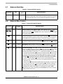
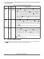
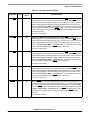
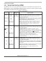
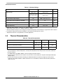
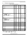
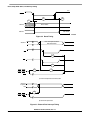
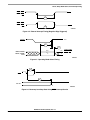
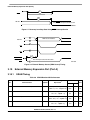
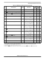
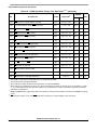
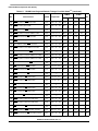
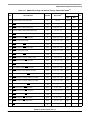
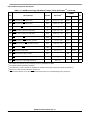
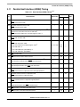
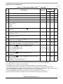
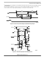
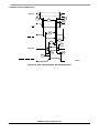
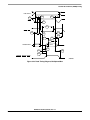
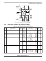
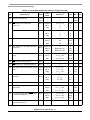
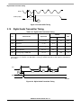
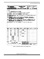
3
3.1
Specifications
Introduction
The DSP56367 is a high density CMOS device with Transistor-Transistor Logic (TTL) compatible inputs
and outputs.
NOTE
This document contains information on a new product. Specifications and
information herein are subject to change without notice.
Finalized specifications may be published after further characterization and device qualifications are
completed.
3.2
Maximum Ratings
CAUTION
This device contains circuitry protecting against damage due to high static
voltage or electrical fields. However, normal precautions should be taken to
avoid exceeding maximum voltage ratings. Reliability of operation is
enhanced if unused inputs are pulled to an appropriate logic voltage level
(for example, either GND or VCC). The suggested value for a pull-up or
pull-down resistor is 10 kΩ.
NOTE
In the calculation of timing requirements, adding a maximum value of one
specification to a minimum value of another specification does not yield a
reasonable sum. A maximum specification is calculated using a worst case
variation of process parameter values in one direction. The minimum
specification is calculated using the worst case for the same parameters in
the opposite direction. Therefore, a “maximum” value for a specification
will never occur in the same device that has a “minimum” value for another
specification; adding a maximum to a minimum represents a condition that
can never exist.
DSP56367 Technical Data, Rev. 2.1
Freescale Semiconductor
3-1