1
DATA SHEET
MOS INTEGRATED CIRCUIT
µPD800261
ERTEC 200
Enhanced Real-Time Ethernet Controller
with 32-bit RISC CPU Core
DESCRIPTION
ERTEC 200 is a powerful communication block for development of industrial Ethernet devices. ERTEC
200 contains a 32-bit RISC processor, an external memory interface with SDRAM and SRAM controller, an LBU interface, a 2-channel real-time Ethernet interface with integrated PHYs, synchronous and
asynchronous serial ports, and general purpose I/Os. Its robust construction, specific automation functions, and openness to the IT world are distinguishing features. The ERTEC 200 is housed in a 304-pin
plastic FBGA package (19 mm × 19 mm).
Detailed functions are described in the following user’s manual. Be sure to read this manual
when you design your systems.
User’s Manual ERTEC 200
: A17988EE2V0UM00
FEATURES
•
•
•
•
•
•
ARM946E-S core with max. 150 MHz
- 8 kBytes of instruction cache
- 4 kBytes of data cache
- 4 kBytes of D-TCM
- Memory protection unit
- On-chip debug and trace functionality via
JTAG interface
- ETM9 embedded trace macrocell
- Interrupt controller for 16 IRQs and 8 FIQs
Internal Multilayer AHB bus running at 50 MHz
External memory interface (EMIF) supports up
to 128 MBytes of SDRAM and up to 64 MBytes
for static memories and I/O with 4 chip selects
Single-channel DMA controller for high-speed
memory-to-memory transfers and for serial
interface support
Integrated PLL to generate internal clocks for
ARM946E-S, AHB, APB and IRT switch
Predefined Boot ROM content supporting
different download sources
•
•
•
•
•
•
•
•
•
Local bus unit (LBU) with 16-bit data bus to
connect external host with access to internal
ERTEC 200 resources
IRT switch block with 2 Ethernet ports
(10/100 Mbps) supporting RT and IRT traffic
- integrated Ethernet PHYs
- autonegotiation, broadcast filter
- 64 kBytes internal communication SRAM
one UART (16550 like) and one SPI interface
two 32-bit timers with prescaler, one 16-bit
timer, one 32-bit F-timer and two watchdog
timers
Max. 45 GPIOs, partly usable as interrupts
- Max. 32 GPIOs, if LBU interface is used
Various configuration options selectable during
reset
1.5 V (logic) and 3.3 V (I/O) power supply
Temperature range: TA = -40 to 85°C
Compact 304-pin plastic FBGA package
ORDERING INFORMATION
Device
ERTEC 200
Remark:
Part Number
µPD800261F1-816-HN2-A
Package
P-FBGA304, 19 × 19 mm
Products with -A at the end of the part number are lead-free products.
The information in this document is subject to change without notice. Before using this document, please confirm that
this is the latest version.
Not all products and/or types are available in every country. Please check with an NEC Electronics sales representative
for availability and additional information.
© NEC Electronics Corporation 2009
Document No. A17989EE2V0DS00
Data Published: November 2009
µPD800261
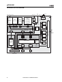
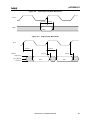
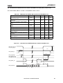
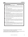
INTERNAL BLOCK DIAGRAM
4RACE
0ORT
*4!'$EBUG
%XTERNAL-EMORY)NTERFACE
-(Z
2%&?#,+
%-)&
-ASTER
3LAVE
3LAVE
%4!0"
-ASTER
3LAVE
-(Z
-(Z
)#ACHEK"YTES
$#ACHEK"YTES
$4#-K"YTES
-(Z
3LAVE
$-!
#ONTROLLER
!2)NTERRUPT
#ONTROLLER
!2-
#LOCK
"3
4!0
WITH
%XTERNAL
-EMORY
)NTERFACE
2ESET
#LOCK
5NIT
"OOT
2/K"YTES
3LAVE
!2-%3
'0)/
BIT-(Z
3LAVE
-ASTER
-#"USBIT-(Z
-ASTER
,OCAL
"US5NIT
3#"USBIT-(Z
#OMMUNI
CATION
32!-
3WITCH#ONTROL
K"YTES
,"5
BIT
-58
,OCAL"US
'0)/%4--))
2
%THERNET
#HANNEL
%THERNET
#HANNEL
0ORT
0ORT
0(9
0(9
0ORT
0ORT
-$)0ORT
-$)0ORT
)24
3WITCH
-ACRO
Data Sheet A17989EE2V0DS00
30)
)NTERFACE
X4IMER
7ATCHDOG
&4IMER
3YSTEM
#ONTROL
2EGISTERS
0ERIPHERAL0ORTS
3LAVE
!("
7RAPPER
3LAVE
-ASTER
!("
7RAPPER
5!24
3LAVE
-58!RB
3LAVE
-ULTILAYER!("
BIT-(Z
)NPUT
STAGE
3LAVE
)NPUT
STAGE
!("!0"
"RIDGE
-ASTER
)NPUT
STAGE
$ECODE
-58!RB
$ECODE
3LAVE
)NPUT
STAGE
-58!RB
'0)/
5!24
30)
4IMER
7ATCHDOG
-#?0,,
µPD800261
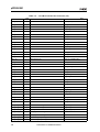
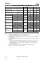
PIN IDENTIFICATION
(1/2)
A(23:0)
: Address bus
SPI1_SSPRXD
: SPI receive data
D(31:0)
: Data bus
SPI1_SSPTXD
: SPI transmit data
WR_N
: Write strobe
SPI1_SCLKOUT
: SPI clock out
RD_N
: Read strobe
SPI1_SFRMOUT
: SPI serial frame output
CLK_SDRAM
: Clock to SDRAM
SPI1_SFRMIN
: SPI serial frame input
BE(3:0)_DQM(3:0)_N
: Byte enable
SPI1_SCLKIN
: SPI clock in
CS_SDRAM_N
: Chip select to SDRAM
SPI1_SSPCTLOE
: SPI clock and serial frame
output enable
RAS_SDRAM_N
: Row address strobe to
SDRAM
SPI1_SSPOE
: SPI output enable
CAS_SDRAM_N
: Column address strobe to
SDRAM
TXD_P(2:1) 0
: MII transmit data bit 0
WE_SDRAM_N
: RD/WR SDRAM
TXD_P(2:1) 1
: MII transmit data bit 1
CS_PER(3:0)_N
: Chip select
TXD_P(2:1) 2
: MII transmit data bit 2
RDY_PER_N
: Ready signal
TXD_P(2:1) 3
: MII transmit data bit 3
DTR_N
: Direction signal for external
driver or scan clock
RXD_P(2:1) 0
: MII receive data bit 0
OE_DRIVER_N
: Enable signal for external
driver or scan clock
RXD_P(2:1) 1
: MII receive data bit 1
BOOT(3:0)
: Boot mode
RXD_P(2:1) 2
: MII receive data bit 2
CONFIG(6:1)
: System configuration
RXD_P(2:1) 3
: MII receive data bit 3
GPIO(44:0)
: GPIO pins
TX_EN_P(2:1)
: MII transmit enable
UART-TXD
: UART transmit data output
TX_ERR_P(2:1)
: MII transmit error
UART-RXD
: UART receive data input
RX_ER_P(2:1)
: MII receive error
UART-DCD_N
: UART carrier detection
signal
CRS_P(2:1)
: MII carrier sense
UART-DSR_N
: UART data set ready signal
RX_DV_P(2:1)
: MII receive data valid
UART-CTS_N
: UART transmit enable
signal
COL_P(2:1)
: MII collision
LBU_A(20:0)
: LBU address bus
RX_CLK_P(2:1)
: MII receive clock
LBU_D(15:0)
: LBU data bus
TX_CLK_P(2:1)
: MII transmit clock
LBU_WR_N
: LBU write control
SMI_MDC
: MII SMI clock
LBU_RD_N
: LBU read control
SMI_MDIO
: MII SMI input/output
LBU_BE(1:0)_N
: LBU byte enable
RES_PHY_N
: Reset to PHY
LBU_SEG_(1:0)
: LBU page selection
P(2:1)TxP
: Differential transmit output
LBU_IRQ_(1:0)_N
: LBU interrupt request
P(2:1)TxN
: Differential transmit output
LBU_RDY_N
: LBU ready signal
P(2:1)RxP
: Differential receive input
LBU_CS_M_N
: LBU chip select to ERTEC
200 internal resources
P(2:1)RxN
: Differential receive input
LBU_CS_R_N
: LBU chip select to page
configuration registers
P(2:1)TDxP
: FX differential transmit output
Data Sheet A17989EE2V0DS00
3
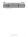
µPD800261
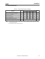
(2/2)
P(2:1)TDxN
: FX differential transmit output
DBGREQ
: Debug request to ARM9
P(2:1)RDxP
: FX differential receive input
DBGACK
: Debug acknowledge
P(2:1)RDxN
: FX differential receive input
TAP_SEL
: Select TAP controller
P(2:1)SDxP
: FX differential SD input
CLKP_A
: Quartz connection
P(2:1)SDxN
: FX differential SD input
CLKP_B
: Quartz connection
EXTRES
: Reference resistor 12.4 kΩ
REF_CLK
: Reference clock output
P(2:1)DUPLEX-LED_N
: PHY LED
F_CLK
: Clock for F-counter
P(2:1)LINK-LED_N
: PHY LED
RESET_N
: Power On reset
P(2:1)-SPEED-100LED_N
(TX/FX)
: PHY LED
WD_WDOUT0_N
: Watchdog output
: PHY LED
VDD Core
: Power supply for core,
1.5 V
P(2:1)-RX-LED_N
: PHY LED
GND Core
: GND for core
P(2:1)-TX-LED_N
: PHY LED
VDD IO
: Power supply for IO, 3.3 V
P(2:1)-ACTIVE-LED_N
: PHY LED
GND IO
: GND for IO
PLL_EXT_IN_N
: MC_PLL input signal
PLL_AVDD
: Analog power supply for
PLL, 1.5 V
TGEN_OUT1_N
: MC_PLL output signal
PLL_AGND
: Analog GND for PLL
TRACEPKT(7:0)
: Trace pins of ETM
VDDQ (PECL)
: Power supply for PECL
buffers, 3.3 V
ETMEXTOUT
: ETM output signal
GND (PECL)
: GND for PECL buffers
ETMEXTIN1
: ETM input signal
DVDD(4:1)
: Digital power supply for
PHYs, 1.5 V
PIPESTA(2:0)
: Trace pipeline status
DGND(4:1)
: Digital GND for PHYs
TRACESYNC
: Trace sync signal
P(2:1)VDDARXTX
: Analog port Tx/Rx power
supply, 1.5 V
TRACECLK
: ETM trace or scan clock
P(2:1)VSSARX
: Analog port GND
P(2:1)-SPEED-10LED_N
TRST_N
: JTAG reset
P(2:1)VSSATX(2:1)
: Analog port GND
TCK
: JTAG clock
VDDAPLL
: Analog central power supply, 1.5 V
TDI
: JTAG data in
VDDACB
: Analog central power supply, 3.3 V
TMS
: JTAG test mode select
VSSAPLLCB
: Analog central GND
TDO
: JTAG data out
VDD33ESD
: Analog test power supply,
3.3 V
SRST_N
: Hardware reset for debug
usage
GND33ESD
: Analog test GND
4
Data Sheet A17989EE2V0DS00
µPD800261
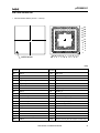
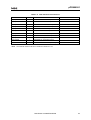
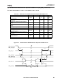
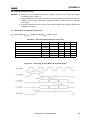
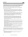
PIN CONFIGURATION
•
304-Pin Plastic FBGA (19 mm × 19 mm)
22
21
20
19
18
17
16
15
14
13
12
11
10
9
8
7
6
5
4
3
2
1
INDEX MARK
AA W U R N L J G E C A
AB Y V T P M K H F D B
(1/5)
Pin
Number
Pin Name
Pin
Number
Pin Name
A2
VDD IO
A21
GND Core
A3
A1
B1
GND IO
A4
WR_N
B2
A3
A5
CS_PER1_N
B3
A2
A6
CS_PER2_N
B4
A0
A7
GPIO26
B5
RD_N
A8
GND IO
B6
CS_PER3_N
A9
VDD IO
B7
RESET_N
A10
VDD IO
B8
GPIO30
A11
GPIO21/SPI1_SFRMOUT
B9
GPIO25/TGEN_OUT1_N
A12
GND IO
B10
GPIO27
A13
GPIO16/SPI1_SSPCTLOE
B11
GPIO24/PLL_EXT_IN_N
A14
VDD IO
B12
GPIO18/SPI1_SSPRXD
A15
REF_CLK
B13
F_CLK
A16
GPIO12/UART-CTS-N
B14
CLKP_A
A17
GPIO9/UART-RXD
B15
GPIO13
A18
VDD IO
B16
GPIO10/UART-DCD-N
A19
GPIO4/P1-LINK-LED_N
B17
GPIO8/UART-TXD
A20
GND IO
B18
GPIO6/P1-RX-LED_N/P1-TX-LED_N/P1-ACTIVE-LED_N
Data Sheet A17989EE2V0DS00
5
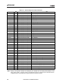
µPD800261
(2/5)
Pin
Number
Pin
Number
Pin Name
Pin Name
B19
GPIO3/P2-SPEED-100LED_N/P2-SPEED-10LED_N
E13
VDD Core
B20
GPIO1/P2 -DUPLEX-LED_N
E14
GPIO15/WD_WDOUT0_N
B21
GND IO
E15
GPIO14/DBGACK
B22
VDD IO
E16
GPIO11/UART-DSR-N
C1
A6
E17
GND Core
C2
A5
E18
VDD Core
C21
P1TDxP
E19
GNDNote
C22
P1TDxN
E21
P1RDxN
D1
A8
E22
P1RDxP
D2
A7
F1
A12
D4
A4
F2
A11
D5
CS_PER0_N
F4
A20/CONFIG3
D6
VDD Core
F5
GND Core
D7
RDY_PER_N
F6
VDD Core
D8
OE_DRIVER_N
F7
GND Core
D9
VDD Core
F8
GND IO
D10
GPIO23/SPI1_SCLKIN
F9
GPIO28
D11
GPIO20/SPI1_SCLKOUT
F10
GPIO22/SPI1_SFRMIN/DBGACK
D12
VDD Core
F13
PLL_AGND
D13
GPIO19/SPI1_SSPTXD
F14
GPIO17/SPI1_SSPOE
D14
CLKP_B
F15
GND IO
D15
GPIO7/P2-RX-LED_N/P2-TX-LED_N/P2-ACTIVE-LED_N
F16
GND Core
D16
GPIO5/P2-LINK-LED_N
F17
VDD Core
D17
GPIO2/P1-SPEED-100LED_N/P1-SPEED-10LED_N
F18
GND (PECL)
D18
VDD Core
F19
P1SDxN
D19
GPIO0/P1-DUPLEX-LED_N
F21
GNDNote
D21
VDDQ (PECL)
F22
VDD33ESD
D22
VDDQ (PECL)
G1
A14
E1
A10
G2
A13
E2
A9
G4
A21/CONFIG4
E4
A19/CONFIG2
G5
GND IO
E5
VDD Core
G6
GND Core
E6
GND Core
G17
DGND2
E7
DTR_N/BOOT0
G18
DVDD1
E8
GPIO31/DBGREQ
G19
P1SDxP
E9
GPIO29
G21
P1RxP
E10
GND IO
G22
P1RxN
E11
GND Core
H1
VDD IO
E12
PLL_AVDD
H2
A15/BOOT1
Note: Connect to GND to improve heat dissipation; pins may as well be left open.
6
Data Sheet A17989EE2V0DS00
µPD800261
(3/5)
Pin
Number
Pin Name
Pin
Number
Pin Name
H4
A23/CONFIG6
M4
WE_SDRAM_N
H5
A22/CONFIG5
M5
RAS_SDRAM_N
H6
GND IO
M18
P2VSSATX1
H17
GNDNote
M19
GNDNote
H18
GND33ESD
M21
P2TxN
H19
DVDD2
M22
P2TxP
H21
DGND1
N1
VDD IO
H22
VDDACB
N2
D1
J1
GND IO
N4
BE0_DQM0_N
J2
A16/BOOT2
N5
D20
J4
BE2_DQM2_N
N6
D21
J5
leave open
N17
P2VSSARX
J6
D18
N18
P2VDDARXTX
J17
P1VSSARX
N19
GNDNote
J18
GNDNote
N21
GNDNote
J19
P1VDDARXTX
N22
GNDNote
J21
P1TxN
P1
D2
J22
P1TxP
P2
D3
K1
A18/CONFIG1
P4
D25
K2
A17/BOOT3
P5
BE3_DQM3_N
K4
D16
P6
D22
K5
D17
P17
GNDNote
K6
D19
P18
GNDNote
K17
P1VSSATX1
P19
GNDNote
K18
P1VSSATX2
P21
P2RxP
K19
VDDAPLL
P22
P2RxN
K21
GNDNote
R1
D4
K22
GND
Note
R2
VDD Core
L1
CS_SDRAM_N
R4
D26
L2
CAS_SDRAM_N
R5
D23
L4
VDD Core
R6
D24
L5
GND Core
R17
DGND3
L18
VSSAPLLCB
R18
GNDNote
L19
P2VSSATX2
R19
VDDQ (PECL)
L21
EXTRES
R21
DVDD4
L22
leave open
R22
DVDD3
M1
CLK_SDRAM
T1
GND IO
M2
D0
T2
D5
Note: Connect to GND to improve heat dissipation; pins may as well be left open.
Data Sheet A17989EE2V0DS00
7
µPD800261
(4/5)
Pin
Number
Pin Name
Pin
Number
Pin Name
T4
D27
V15
LBU_D13/SMI_MDIO
T5
leave open
V16
LBU_D14/RES_PHY_N
T6
GND Core
V17
GND IO
T17
DGND4
V18
VDD Core
T18
GND (PECL)
V19
P2SDxP
T19
GND (PECL)
V21
VDDQ (PECL)
T21
VDD Core
V22
GNDNote
T22
GNDNote
W1
D9
U1
D6
W2
D10
U2
D7
W4
D29
U4
D28
W5
D30
U5
GND IO
W6
D31
U6
VDD Core
W7
TCK
U7
GND IO
W8
TAP_SEL
U8
VDD Core
W9
LBU_A16/GPIO32
U9
TDI
W10
LBU_A17/GPIO33
U10
TRST_N
W11
LBU_A15/COL_P2
U13
LBU_SEG_1/GPIO38
W12
LBU_A19/GPIO35
U14
LBU_CS_M_N/GPIO40
W13
VDD Core
U15
GND IO
W14
LBU_D12/SMI_MDC
U16
GND Core
W15
LBU_D1/TXD_P11
U17
VDD Core
W16
LBU_D15/GPIO41
U18
P2SDxN
W17
VDD Core
U19
leave open
W18
LBU_IRQ1_N/GPIO44
U21
P2RDxN
W19
LBU_RDY_N/GPIO42
U22
P2RDxP
W21
P2TDxN
V1
BE1_DQM1_N
W22
VDD IO
V2
D8
Y1
VDD IO
V4
VDD Core
Y2
D11
V5
VDD Core
Y21
P2TDxP
V6
GND Core
Y22
VDD IO
V7
TMS
AA1
D12
V8
SRST_N
AA2
D13
V9
TDO
AA3
D15
V10
LBU_A18/GPIO34
AA4
LBU_A1/RXD_P11/ETMEXTIN1
V11
GND Core
AA5
LBU_A2/RXD_P12/TRACEPKT7
V12
LBU_A20/GPIO36
AA6
LBU_A4/CRS_P1/TRACEPKT5
V13
LBU_SEG_0/GPIO37
AA7
LBU_A6/RX_DV_P1/TRACEPKT3
V14
GND Core
AA8
LBU_A8/RXD_P20/TRACEPKT1
Note: Connect to GND to improve heat dissipation; pins may as well be left open.
8
Data Sheet A17989EE2V0DS00
µPD800261
(5/5)
Pin
Number
Pin
Number
Pin Name
Pin Name
AA9
LBU_A10/RXD_P22/TRACESYNC
AB5
LBU_A3/RXD_P13/TRACEPKT6
AA10
LBU_A11/RXD_P23/PIPESTA2
AB6
LBU_A5/RX_ER_P1/TRACEPKT4
AA11
LBU_A13/RX_ER_P2/PIPESTA0
AB7
LBU_A7/COL_P1/TRACEPKT2
AA12
LBU_WR_N/TX_CLK_P1
AB8
LBU_A9/RXD_P21/TRACEPKT0
AA13
LBU_BE1_N/RX_CLK_P2
AB9
VDD IO
AA14
LBU_D0/TXD_P10
AB10
LBU_A12/CRS_P2/PIPESTA1
AA15
VDD Core
AB11
LBU_A14/RX_DV_P2
AA16
LBU_D3/TXD_P13
AB12
LBU_CS_R_N/GPIO39
AA17
LBU_D5/TX_ERR_P1
AB13
LBU_RD_N/TX_CLK_P2
AA18
LBU_D7/TXD_P21
AB14
LBU_BE0_N/RX_CLK_P1
AA19
LBU_D9/TXD_P23
AB15
VDD IO
AA20
LBU_D10/TX_EN_P2
AB16
LBU_D2/TXD_P12
AA21
LBU_IRQ0_N/GPIO43
AB17
LBU_D4/TX_EN_P1
AA22
GND Core
AB18
LBU_D6/TXD_P20
AB2
D14
AB19
LBU_D8/TXD_P22
AB3
LBU_A0/RXD_P10/ETMEXTOUT
AB20
VDD IO
AB4
TRACECLK
AB21
LBU_D11/TX_ERR_P2
Data Sheet A17989EE2V0DS00
9
µPD800261
Table of Contents
1.
Pin Functions . . . . . . . . . . . . . . . . . . . . . . . . . . . . . . . . . . . . . . . . . . . . . . . . . 13
1.1
1.2
1.3
List of Pin Functions . . . . . . . . . . . . . . . . . . . . . . . . . . . . . . . . . . . . . . . . . . . . . . . . . . . 13
Pin Characteristics . . . . . . . . . . . . . . . . . . . . . . . . . . . . . . . . . . . . . . . . . . . . . . . . . . . . 24
Pin Status and Recommended Connections . . . . . . . . . . . . . . . . . . . . . . . . . . . . . . . 26
2.1
2.2
2.3
2.4
Absolute Maximum Ratings . . . . . . . . . . . . . . . . . . . . . . . . . . . . . . . . . . . . . . . . . . . . . 30
Operating Conditions . . . . . . . . . . . . . . . . . . . . . . . . . . . . . . . . . . . . . . . . . . . . . . . . . . 31
Thermal Characteristics . . . . . . . . . . . . . . . . . . . . . . . . . . . . . . . . . . . . . . . . . . . . . . . . 33
AC Characteristics . . . . . . . . . . . . . . . . . . . . . . . . . . . . . . . . . . . . . . . . . . . . . . . . . . . . . 34
2.4.1
Clock timing . . . . . . . . . . . . . . . . . . . . . . . . . . . . . . . . . . . . . . . . . . . . . . . . . . . . 34
2.4.2
I/O timing specifications . . . . . . . . . . . . . . . . . . . . . . . . . . . . . . . . . . . . . . . . . . . 36
2.4.3
LBU timing specifications . . . . . . . . . . . . . . . . . . . . . . . . . . . . . . . . . . . . . . . . . . 38
2.4.4
SPI timing specifications . . . . . . . . . . . . . . . . . . . . . . . . . . . . . . . . . . . . . . . . . . . 43
2.4.5
Power-up sequence . . . . . . . . . . . . . . . . . . . . . . . . . . . . . . . . . . . . . . . . . . . . . . 45
2.4.6
Reset timing . . . . . . . . . . . . . . . . . . . . . . . . . . . . . . . . . . . . . . . . . . . . . . . . . . . . 46
2.
Electrical Specifications . . . . . . . . . . . . . . . . . . . . . . . . . . . . . . . . . . . . . . . . 30
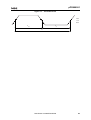
3.
Package Drawing . . . . . . . . . . . . . . . . . . . . . . . . . . . . . . . . . . . . . . . . . . . . . . 47
4.
Recommended Soldering Conditions . . . . . . . . . . . . . . . . . . . . . . . . . . . . . 48
10
Data Sheet A17989EE2V0DS00
µPD800261
List of Figures
Figure 2-1:
Figure 2-2:
Figure 2-3:
Figure 2-4:
Figure 2-5:
Figure 2-6:
Figure 2-7:
Figure 2-8:
Figure 2-9:
Figure 2-10:
Figure 2-11:
Figure 3-1:
Clock Waveforms ........................................................................................................ 35
Input Setup and Hold Waveforms ............................................................................... 37
Output Delay Waveforms ............................................................................................ 37
LBU Read from ERTEC 200 with Separate Read/Write line ....................................... 39
LBU Write to ERTEC 200 with Separate Read/Write line ........................................... 40
LBU Read from ERTEC 200 with Common Read/Write line ....................................... 41
LBU Write to ERTEC 200 with Common Read/Write line ........................................... 42
SPI Timing in Slave Mode (TI-format Example) .......................................................... 43
SPI Timing in Master Mode (TI-format Example) ........................................................ 44
Power-Up Sequence Timing Diagram ......................................................................... 45
Reset Timing Diagram................................................................................................. 46
Package Drawing ........................................................................................................ 47
Data Sheet A17989EE2V0DS00
11
µPD800261
List of Tables
Table 1-1:
Table 1-2:
Table 1-3:
Table 1-4:
Table 1-5:
Table 1-6:
Table 1-7:
Table 1-8:
Table 1-9:
Table 1-10:
Table 1-11:
Table 1-12:
Table 1-13:
Table 1-14:
Table 1-15:
Table 1-16:
Table 2-1:
Table 2-2:
Table 2-3:
Table 2-4:
Table 2-5:
Table 2-6:
Table 2-7:
Table 2-8:
Table 2-9:
Table 2-10:
Table 2-11:
Table 4-1:
12
External Memory Interface Pin Functions....................................................................... 13
Local Bus Interface Pin Functions .................................................................................. 14
MII Diagnosis Interface Pin Functions ............................................................................ 16
PHY Interface Pin Functions .......................................................................................... 17
General Purpose I/O Pin Functions................................................................................ 18
UART Pin Functions ....................................................................................................... 19
SPI1 Pin Functions ......................................................................................................... 19
MC_PLL Pin Functions................................................................................................... 19
Clock and Reset Pin Functions ...................................................................................... 20
JTAG and Debug Interface Pin Functions ...................................................................... 20
Trace Port Pin Functions ................................................................................................ 21
Power Supply Pin Functions........................................................................................... 22
Alternative Functions of GPIO(31:0) Pins....................................................................... 23
Pin Characteristics.......................................................................................................... 24
Pin Status During Reset and Recommended Connections............................................ 26
Alternative Functions of LBU Interface Pins ................................................................... 28
Absolute Maximum Ratings............................................................................................ 30
Recommended Operating Conditions ............................................................................ 31
Thermal Characteristics of Package............................................................................... 33
Clock AC Characteristics................................................................................................ 34
I/O Timing Specifications................................................................................................ 36
LBU Read from ERTEC 200 with Separate Read/Write line .......................................... 39
LBU Write to ERTEC 200 with Separate Read/Write line .............................................. 40
LBU Read from ERTEC 200 with Common Read/Write line .......................................... 41
LBU Write to ERTEC 200 with Common Read/Write line .............................................. 42
SPI Timing Specifications (slave mode) ......................................................................... 43
SPI Timing Specifications (master mode) ...................................................................... 44
Soldering Conditions for Lead-free Device..................................................................... 48
Data Sheet A17989EE2V0DS00
µPD800261
1. Pin Functions
1.1 List of Pin Functions
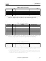
Table 1-1:
Pin Name
External Memory Interface Pin Functions
I/O
Function
Alternate Function
A(23:18)
I/ONote External memory address bus (23:18)
CONFIG(6:1)Note
A(17:15)
I/ONote External memory address bus (17:15)
BOOT(3:1)Note
A(14:0)
O
External memory address bus (14:0)
-
D(31:0)
I/O
External memory data bus (31:0)
-
WR_N
O
Write strobe signal
-
RD_N
O
Read strobe signal
-
CLK_SDRAM
O
Clock to SDRAM
-
CS_SDRAM_N
O
Chip select to SDRAM
-
RAS_SDRAM_N
O
Row address strobe to SDRAM
-
CAS_SDRAM_N
O
Column address strobe to SDRAM
-
WE_SDRAM_N
O
RD/WR signal to SDRAM
-
CS_PER(3:0)_N
O
Chip select to static memories and peripherals
-
BE(3:0)_DQM(3:0)_N
O
Byte enable signal
-
I
Ready signal
-
Direction signal for external driver or scan clock
BOOT0Note
Enable signal for external driver or scan clock
-
RDY_PER_N
DTR_N
OE_DRIVER_N
I/ONote
O
Note: The BOOT(3:0) and CONFIG(6:1) pins are used as inputs and read into the BOOT_REG respectively
CONFIG_REG system configuration registers during the active Power On reset phase. After a reset,
these pins are available as normal function pins and used as outputs.
Data Sheet A17989EE2V0DS00
13
µPD800261
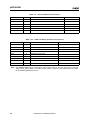
Table 1-2:
Pin Name
Local Bus Interface Pin Functions (1/2)
I/ONote
Function
Alternate FunctionNote
LBU_A(20:16)
I
LBU address bits
GPIO(36:32)
LBU_A15
I
LBU address bit 15
COL_P2
LBU_A14
I
LBU address bit 14
RX_DV_P2
LBU_A13
I
LBU address bits 13
RX_ER_P2/PIPESTA0
LBU_A12
I
LBU address bit 12
CRS_P2/PIPESTA1
LBU_A11
I
LBU address bit 11
RXD_P23/PIPESTA2
LBU_A10
I
LBU address bit 10
RXD_P22/TRACESYNC
LBU_A9
I
LBU address bit 9
RXD_P21/TRACEPKT0
LBU_A8
I
LBU address bit 8
RXD_P20/TRACEPKT1
LBU_A7
I
LBU address bit 7
COL_P1/TRACEPKT2
LBU_A6
I
LBU address bit 6
RX_DV_P1/TRACEPKT3
LBU_A5
I
LBU address bit 5
RX_ER_P1/TRACEPKT4
LBU_A4
I
LBU address bit 4
CRS_P1/TRACEPKT5
LBU_A3
I
LBU address bit 3
RXD_P13/TRACEPKT6
LBU_A2
I
LBU address bit 2
RXD_P12/TRACEPKT7
LBU_A1
I
LBU address bit 1
RXD_P11/ETMEXTIN1
LBU_A0
I
LBU address bit 0
RXD_P10/ETMEXTOUT
LBU_D15
I/O
LBU data bit 15
GPIO41
LBU_D14
I/O
LBU data bit 14
RES_PHY_N
LBU_D13
I/O
LBU data bit 13
SMI_MDIO
LBU_D12
I/O
LBU data bit 12
SMI_MDC
LBU_D11
I/O
LBU data bit 11
TX_ERR_P2
LBU_D10
I/O
LBU data bit 10
TX_EN_P2
LBU_D9
I/O
LBU data bit 9
TXD_P23
LBU_D8
I/O
LBU data bit 8
TXD_P22
LBU_D7
I/O
LBU data bit 7
TXD_P21
LBU_D6
I/O
LBU data bit 6
TXD_P20
LBU_D5
I/O
LBU data bit 5
TX_ERR_P1
LBU_D4
I/O
LBU data bit 4
TX_EN_P1
LBU_D3
I/O
LBU data bit 3
TXD_P13
LBU_D2
I/O
LBU data bit 2
TXD_P12
LBU_D1
I/O
LBU data bit 1
TXD_P11
LBU_D0
I/O
LBU data bit 0
TXD_P10
LBU_WR_N
I
LBU write control signal
TX_CLK_P1
LBU_RD_N
I
LBU read control signal
TX_CLK_P2
LBU_BE(1:0)_N
I
LBU byte enable
RX_CLK_P(2:1)
LBU_SEG_1
I
LBU page selection signal
GPIO38
LBU_SEG_0
I
LBU page selection signal
GPIO37
LBU_IRQ_1_N
O
LBU interrupt request signal
GPIO44
LBU_IRQ_0_N
O
LBU interrupt request signal
GPIO43
14
Data Sheet A17989EE2V0DS00
µPD800261
Table 1-2:
Pin Name
Local Bus Interface Pin Functions (2/2)
I/ONote
Function
Alternate FunctionNote
LBU_RDY_N
O
LBU ready signal
GPIO42
LBU_CS_M_N
I
LBU chip select for ERTEC 200 internal resources GPIO40
LBU_CS_R_N
I
LBU chip select for page configuration registers
GPIO39
Note: Local bus interface pins are alternatively used as MII diagnosis, trace or GPIO pins; in this table the I/O
type is listed for the local bus function.
Data Sheet A17989EE2V0DS00
15
µPD800261
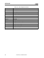
Table 1-3: MII Diagnosis Interface Pin Functions
Pin NameNote
I/O
Function
Alternate FunctionNote
SMI_MDC
O
Serial management interface clock
LBU_D12
SMI_MDIO
O
Serial management interface data input/output
LBU_D13
RES_PHY_N
O
Reset signal to PHYs
LBU_D14
TXD_P2(3:0)
O
Transmit data port 2 bits
LBU_D(9:6)
RXD_P23
O
Receive data port 2 bit 3
LBU_A11/PIPESTA2
RXD_P22
O
Receive data port 2 bit 2
LBU_A10/TRACESYNC
RXD_P21
O
Receive data port 2 bit 1
LBU_A9/TRACEPKT0
RXD_P20
O
Receive data port 2 bit 0
LBU_A8/TRACEPKT1
TX_EN_P2
O
Transmit enable port 2
LBU_D10
CRS_P2
O
Carrier sense port 2
LBU_A12/PIPESTA1
RX_ER_P2
O
Receive error port 2
LBU_A13/PIPESTA0
TX_ERR_P2
O
Transmit error port 2
LBU_D11
RX_DV_P2
O
Receive data valid port 2
LBU_A14
COL_P2
O
Collision port 2
LBU_A15
RX_CLK_P2
O
Receive clock port 2
LBU_BE1_N
TX_CLK_P2
O
Transmit clock port 2
LBU_RD_N
TXD_P1(3:0)
O
Transmit data port 1 bits
LBU_D(3:0)
RXD_P13
O
Receive data port 1 bit 3
LBU_A3/TRACEPKT6
RXD_P12
O
Receive data port 1 bit 2
LBU_A2/TRACEPKT7
RXD_P11
O
Receive data port 1 bit 1
LBU_A1/ETMEXTIN1
RXD_P10
O
Receive data port 1 bit 0
LBU_A0/ETMEXTOUT
TX_EN_P1
O
Transmit enable port 1
LBU_D4
CRS_P1
O
Carrier sense port 1
LBU_A4/TRACEPKT5
RX_ER_P1
O
Receive error port 1
LBU_A5/TRACEPKT4
TX_ERR_P1
O
Transmit error port 1
LBU_D5
RX_DV_P1
O
Receive data valid port 1
LBU_A6/TRACEPKT3
COL_P1
O
Collision port 1
LBU_A7/TRACEPKT2
RX_CLK_P1
O
Receive clock port 1
LBU_BE0_N
TX_CLK_P1
O
Transmit clock port 1
LBU_WR_N
Note: MII diagnosis interface pins are alternatively used as local bus interface or trace pins; in this table the
I/O type is listed for the MII diagnosis function
16
Data Sheet A17989EE2V0DS00
µPD800261
Table 1-4: PHY Interface Pin Functions
Pin Name
I/O
Function
Alternate Function
P(2:1)TxN
O
Differential transmit data output
-
P(2:1)TxP
O
Differential transmit data output
-
P(2:1)TDxN
O
Differential FX transmit data output
-
P(2:1)TDxP
O
Differential FX transmit data output
-
P(2:1)RxN
I
Differential receive data input
-
P(2:1)RxP
I
Differential receive data input
-
P(2:1)RDxN
I
Differential FX receive data input
-
P(2:1)RDxP
I
Differential FX receive data input
-
P(2:1)SDxN
I
Differential FX signal detect input
-
P(2:1)SDxP
I
Differential FX signal detect input
-
EXTRES
I/O
External reference resistor (12.4 kΩ) Note -
Note: The external resistor must have a maximum tolerance of 1%.
Data Sheet A17989EE2V0DS00
17
µPD800261
Table 1-5: General Purpose I/O Pin Functions
Pin Name
I/ONote
Alternate FunctionNote
GPIO(44:43)
I/O
General purpose I/O signal
LBU_IRQ(1:0)_N
GPIO42
I/O
General purpose I/O signal
LBU_RDY_N
GPIO41
I/O
General purpose I/O signal
LBU_D15
GPIO40
I/O
General purpose I/O signal
LBU_CS_M_N
GPIO39
I/O
General purpose I/O signal
LBU_CS_R_N
GPIO(38:37)
I/O
General purpose I/O signal
LBU_SEG(1:0)_N
GPIO(36:32)
I/O
General purpose I/O signal
LBU_A(20:16)
GPIO31
I/O
General purpose I/O signal
DBGREQ
GPIO(30:26)
I/O
General purpose I/O signal
-
GPIO25
I/O
General purpose I/O signal
TGEN_OUT1_N
GPIO24
I/O
General purpose I/O signal
PLL_EXT_IN_N
GPIO23
I/O
General purpose I/O signal
SPI1_SCLKIN
GPIO22
I/O
General purpose I/O signal
SPI1_SFRMIN/DBGACK
GPIO21
I/O
General purpose I/O signal
SPI1_SFRMOUT
GPIO20
I/O
General purpose I/O signal
SPI1_CLKOUT
GPIO19
I/O
General purpose I/O signal
SPI1_SSPTXD
GPIO18
I/O
General purpose I/O signal
SPI1_SSPRXD
GPIO17
I/O
General purpose I/O signal
SPI1_SSPOE
GPIO16
I/O
General purpose I/O signal
SPI1_SSPCTLOE
GPIO15
I/O
General purpose I/O signal
WD_WDOUT0_N
GPIO14
I/O
General purpose I/O signal
DBGACK
GPIO13
I/O
General purpose I/O signal
-
GPIO12
I/O
General purpose I/O signal
UART-CTS_N
GPIO11
I/O
General purpose I/O signal
UART-DSR_N
GPIO10
I/O
General purpose I/O signal
UART-DCD_N
GPIO9
I/O
General purpose I/O signal
UART-RXD
GPIO8
I/O
General purpose I/O signal
UART-TXD
GPIO7
I/O
General purpose I/O signal
P2-RX-LED_N/P2-TX-LED_N/P2-ACTIVE-LED_N
GPIO6
I/O
General purpose I/O signal
P1-RX-LED_N/P1-TX-LED_N/P1-ACTIVE-LED_N
GPIO5
I/O
General purpose I/O signal
P2-LINK-LED_N
GPIO4
I/O
General purpose I/O signal
P1-LINK-LED_N
GPIO3
I/O
General purpose I/O signal
P2-SPEED-100LED_N (TX/FX)/P2-SPEED-10LED_N
GPIO2
I/O
General purpose I/O signal
P1-SPEED-100LED_N (TX/FX)/P1-SPEED-10LED_N
GPIO1
I/O
General purpose I/O signal
P2-DUPLEX-LED_N
GPIO0
I/O
General purpose I/O signal
P1-DUPLEX-LED_N
Function
Note: Primary and alternate functions for GPIO(31:0) are selected with the GPIO_PORT_MODE_H and
GPIO_PORT_MODE_L registers; primary and alternate functions for GPIO(44:32) are selected with the
configuration pins. In this table the I/O types are listed for the GPIO function.
18
Data Sheet A17989EE2V0DS00
µPD800261
Table 1-6: UART Pin Functions
Pin Name
I/ONote
Alternate FunctionNote
Function
UART-TXD
O
UART transmit data output
GPIO8
UART-RXD
I
UART receive data input
GPIO9
UART-DCD_N
I
UART carrier detection signal
GPIO10
UART-DSR_N
I
UART data set ready signal
GPIO11
UART-CTS_N
I
UART transmit enable signal
GPIO12
Note: Primary and alternate functions are selected with the GPIO_PORT_MODE_H
GPIO_PORT_MODE_L registers. In this table the I/O types are listed for the UART function.
and
Table 1-7: SPI1 Pin Functions
Pin Name
I/ONote
Function
Alternate FunctionNote
SPI1_SSPRXD
I
SPI1 receive data input
GPIO18
SPI1_SSPTXD
O
SPI1 transmit data output
GPIO19
SPI1_SCLKOUT
O
SPI1 clock output
GPIO20
SPI1_SFRMOUT
O
SPI1 serial frame output signal
GPIO21
SPI1_SFRMIN
I
SPI1 serial frame input signal
GPIO22, DBGACK
SPI1_SCLKIN
I
SPI1 clock input
GPIO23
SPI1_SSPCTLOE
O
SPI1 clock and serial frame output enable
GPIO16
SPI1_SSPOE
O
SPI1 output enable
GPIO17
Note: Primary and alternate functions are selected with the GPIO_PORT_MODE_H
GPIO_PORT_MODE_L registers. In this table the I/O types are listed for the SPI1 function.
and
Table 1-8: MC_PLL Pin Functions
Pin Name
PLL_EXT_IN_N
TGEN_OUT1_N
I/ONote 1
I
O
Function
MC_PLL input signal
MC_PLL output
signalNote 2
Alternate FunctionNote 1
GPIO24
GPIO25
Notes: 1. Primary and alternate functions are selected with the GPIO_PORT_MODE_H register. In this table
the I/O types are listed for the MC_PLL function.
2. For a PROFINET IRT application, GPIO25 must be configured as TGEN_OUT1_N output pin. A synchronous clock signal is then output at this pin; during certification of a PROFINET IO device with
IRT support this signal must be accessible from the outside.
Data Sheet A17989EE2V0DS00
19
µPD800261
Table 1-9: Clock and Reset Pin Functions
Pin Name
I/O
Function
Alternate Function
TRACECLK
O
ETM trace or scan clock
-
CLKP_A
I
Quartz connection
-
CLKP_B
O
Quartz connection
-
F_CLK
I
F_CLK for F-counter
-
REF_CLK
I/O
Reference clock
-
RESET_N
I
Power On reset
-
Table 1-10: JTAG and Debug Interface Pin Functions
Pin Name
I/ONote
Alternate FunctionNote
Function
TRST_N
I
JTAG reset signal
-
TCK
I
JTAG clock signal
-
TDI
I
JTAG data input signal
-
TMS
I
JTAG test mode select signal
-
TDO
O
JTAG data output signal
-
SRST_N
I/O
Hardware reset for debug usage
-
DBGREQ
I
Debug request signal
GPIO31
DBGACK
O
Debug acknowledge signal
GPIO14/GPIO22/SPI1_SFRMIN
TAP_SEL
I
TAP controller select signal
-
Note: The DBGREQ (DBGACK) pin is alternatively used as GPIO (GPIO or SPI1) pin; the function is selected
with the GPIO_PORT_MODE_H and GPIO_PORT_MODE_L registers. In this table the I/O type is listed
for the DBGREQ (DBGACK) function.
20
Data Sheet A17989EE2V0DS00
µPD800261
Table 1-11: Trace Port Pin Functions
Pin Name
I/ONote
Function
Alternate FunctionNote
TRACEPKT7
O
Trace packet bit 7
LBU_A2, RXD_P12
TRACEPKT6
O
Trace packet bit 6
LBU_A3, RXD_P13
TRACEPKT5
O
Trace packet bit 5
LBU_A4, CRS_P1
TRACEPKT4
O
Trace packet bit 4
LBU_A5, RX_ER_P1
TRACEPKT3
O
Trace packet bit 3
LBU_A6, RX_DV_P1
TRACEPKT2
O
Trace packet bit 2
LBU_A7, COL_P1
TRACEPKT1
O
Trace packet bit 1
LBU_A8, RXD_P20
TRACEPKT0
O
Trace packet bit 0
LBU_A9, RXD_P21
PIPESTA2
O
CPU pipeline status, bit 2
LBU_A11, RXD_P23
PIPESTA1
O
CPU pipeline status, bit 1
LBU_A12, CRS_P2
PIPESTA0
O
CPU pipeline status, bit 0
LBU_A13, RX_ER_P2
TRACESYNC
O
Trace sync signal
LBU_A10, RXD_P22
ETMEXTIN1
I
External input to the ETM
LBU_A1, RXD_P11
ETMEXTOUT
O
Output signal from the ETM
LBU_A0, RXD_P10
Note: Trace port pins are alternatively used as local bus or MII diagnosis pins; the function is selected with the
GPIO_PORT_MODE_H and GPIO_PORT_MODE_L registers. In this table the I/O types are listed for
the trace port pin functions.
Data Sheet A17989EE2V0DS00
21
µPD800261
Table 1-12: Power Supply Pin Functions
Pin Name
Function
VDD Core
Power supply for core, 1.5 V
GND Core
GND CORE
VDD IO
Power supply for IO, 3.3 V
GND IO
GND for IO
PLL_AVDD
Analog power supply for PLL, 1.5 V
PLL_AGND
Analog GND for PLL
VDDQ (PECL)
Power supply for PECL buffers, 3.3 V
GND (PECL)
GND for PECL buffers
DVDD(4:1)
Digital power supply, 1.5 V
DGND(4:1)
Digital GND
P(2:1)VSSATX(2:1)
Analog port GND
P(2:1)VDDARXTX
Analog port RX/TX power supply, 1.5 V
P(2:1)VSSARX
Analog port GND
VDDAPLL
Analog central power supply, 1.5 V
VDDACB
Analog central power supply, 3.3 V
VSSAPLLCB
Analog central GND
VDD33ESD
Analog test power supply, 3.3 V
VSS33ESD
Analog test GND
22
Data Sheet A17989EE2V0DS00
µPD800261
Table 1-13:
Alternative Functions of GPIO(31:0) Pins
FunctionNote
GPIO pin
0
1
2
3
after Reset
GPIO0
GPIO0
P1-DUPLEX-LED_N
-
-
GPIO0
GPIO1
GPIO1
P2-DUPLEX-LED_N
-
-
GPIO1
GPIO2
GPIO2
P1-SPEED-100LED_N (TX/FX) P1-SPEED-10LED_N
-
GPIO2
GPIO3
GPIO3
P2-SPEED-100LED_N (TX/FX) P2-SPEED-10LED_N
-
GPIO3
GPIO4
GPIO4
P1-LINK-LED_N
-
-
GPIO4
GPIO5
GPIO5
P2-LINK-LED_N
-
-
GPIO5
GPIO6
GPIO6
P1-RX-LED_N
P1-TX-LED_N
P1-ACTIVE-LED_N GPIO6
GPIO7
GPIO7
P2-RX-LED_N
P2-TX-LED_N
P2-ACTIVE-LED_N GPIO7
GPIO8
GPIO8
UART-TXD
-
-
GPIO8
GPIO9
GPIO9
UART-RXD
-
-
GPIO9
GPIO10
GPIO10
UART-DCD_N
-
-
GPIO10
GPIO11
GPIO11
UART-DSR_N
-
-
GPIO11
GPIO12
GPIO12
UART-CTS_N
-
-
GPIO12
GPIO13
GPIO13
Reserved
-
-
GPIO13
GPIO14
GPIO14
DBGACK
-
-
GPIO14
GPIO15
GPIO15
WD_WDOUT_N
-
-
GPIO15
GPIO16
GPIO16
SPI1_SSPCTLOE
-
-
GPIO16
GPIO17
GPIO17
SPI1_SSPOE
-
-
GPIO17
GPIO18
GPIO18
SPI1_SSPRXD
-
-
GPIO18
GPIO19
GPIO19
SPI1_SSPTXD
-
-
GPIO19
GPIO20
GPIO20
SPI1_SCLKOUT
-
-
GPIO20
GPIO21
GPIO21
SPI1_SFRMOUT
-
-
GPIO21
GPIO22
GPIO22
SPI1_SFRMIN
DBGACK
-
GPIO22
GPIO23
GPIO23
SPI1_SCLKIN
Reserved
-
GPIO23
GPIO24
GPIO24
PLL_EXT_IN_N
-
-
GPIO24
GPIO25
GPIO25
TGEN_OUT1_N
-
-
GPIO25
GPIO(30:26) GPIO(30:26) Reserved
-
-
GPIO(30:26)
GPIO31
-
-
GPIO31
GPIO31
DBGREQ
Note: Alternative functions are software configurable using the GPIO_PORT_MODE_L/H registers.
Data Sheet A17989EE2V0DS00
23
µPD800261
1.2 Pin Characteristics
Table 1-14:
Pin Characteristics (1/2)
Input type
Output type
Internal pull
up/down
Drive capability
I/O
IOH
IOL
A23
I/ONote 1
SchmittNote 1
3.3 V CMOS
50 kΩ pull up
9 mA
9 mA
A22
I/ONote 1
Schmitt
Note 1
3.3 V CMOS
50 kΩ pull down
9 mA
9 mA
A21
I/ONote 1
SchmittNote 1
3.3 V CMOS
50 kΩ pull up
9 mA
9 mA
A20
I/ONote 1
Schmitt
Note 1
3.3 V CMOS
50 kΩ pull down
9 mA
9 mA
A(19:17)
I/ONote 1
Schmitt
Note 1
3.3 V CMOS
50 kΩ pull up
9 mA
9 mA
A(16:15)
I/ONote 1
SchmittNote 1
3.3 V CMOS
50 kΩ pull down
9 mA
9 mA
A(14:0)
O
-
3.3 V CMOS
-
9 mA
9 mA
D(31:0)
I/O
Schmitt
3.3 V CMOS
50 kΩ pull up
9 mA
9 mA
WR_N
O
-
3.3 V CMOS
-
9 mA
9 mA
Pin Name
RD_N
O
-
3.3 V CMOS
-
9 mA
9 mA
CLK_SDRAM
O
-
3.3 V CMOS
-
9 mA
9 mA
CS_SDRAM_N
O
-
3.3 V CMOS
-
9 mA
9 mA
RAS_SDRAM_N
O
-
3.3 V CMOS
-
9 mA
9 mA
CAS_SDRAM_N
O
-
3.3 V CMOS
-
9 mA
9 mA
WE_SDRAM_N
O
-
3.3 V CMOS
-
9 mA
9 mA
CS_PER(3:0)_N
O
-
3.3 V CMOS
-
6 mA
6 mA
BE(3:0)_DQM(3:0)_N
O
-
3.3 V CMOS
-
9 mA
9 mA
I
Schmitt
-
50 kΩ pull up
-
-
SchmittNote 1
3.3 V CMOS
50 kΩ pull up
9 mA
9 mA
RDY_PER_N
Note 1
DTR_N
I/O
OE_DRIVER_N
O
-
3.3 V CMOS
-
9 mA
9 mA
LBU_A(20:0)Note 2
I/O
Schmitt
3.3 V CMOS
50 kΩ pull up
6 mA
6 mA
LBU_D(15:0) Note 2
I/O
Schmitt
3.3 V CMOS
50 kΩ pull up
9 mA
9 mA
LBU_WR_N Note 2
I/O
Schmitt
3.3 V CMOS
50 kΩ pull up
6 mA
6 mA
Note 2
I/O
Schmitt
3.3 V CMOS
50 kΩ pull up
6 mA
6 mA
LBU_BE(1:0)_NNote 2
I/O
Schmitt
3.3 V CMOS
50 kΩ pull up
6 mA
6 mA
LBU_SEG_(1:0) Note 2
I/O
Schmitt
3.3 V CMOS
50 kΩ pull up
6 mA
6 mA
I/O
Schmitt
3.3 V CMOS
50 kΩ pull up
6 mA
6 mA
LBU_RD_N
LBU_IRQ_(1:0)_N
Note 2
LBU_RDY_N Note 2
I/O
Schmitt
3.3 V CMOS
50 kΩ pull up
6 mA
6 mA
LBU_CS_M_N
Note 2
I/O
Schmitt
3.3 V CMOS
50 kΩ pull up
6 mA
6 mA
LBU_CS_R_N
Note 2
I/O
Schmitt
3.3 V CMOS
50 kΩ pull up
6 mA
6 mA
GPIO(31:30) Note 2
I/O
Schmitt
3.3 V CMOS
50 kΩ pull up
6 mA
6 mA
Note 2
I/O
Schmitt
3.3 V CMOS
50 kΩ pull up
24 mA
24 mA
I/O
Schmitt
3.3 V CMOS
50 kΩ pull up
6 mA
6 mA
GPIO(29:27)
GPIO(26:8)
Note 2
GPIO(7:0) Note 2
I/O
Schmitt
3.3 V CMOS
50 kΩ pull up
9 mA
9 mA
CLKP_A
I
Osc. in
-
-
-
-
CLKP_B
O
-
Osc. out
-
6 mA
6 mA
TRACECLK
O
-
3.3 V CMOS
-
18 mA
18 mA
24
Data Sheet A17989EE2V0DS00
µPD800261
Table 1-14:
Pin Name
Pin Characteristics (2/2)
Internal pull
up/down
3.3 V CMOS
-
-
-
-
-
3.3 V CMOS
-
6 mA
6 mA
I
Schmitt
-
50 kΩ pull up
-
-
I/O
Analog
Analog
-
-
-
Input type
F_CLK
I
REF_CLK
O
RESET_N
P(2:1)TxN
P(2:1)TxP
Drive capability
Output type
I/O
IOH
IOL
I/O
Analog
Analog
-
-
-
P(2:1)TDxN
Note 3
O
-
3.3 V CMOS
-
12 mA
12 mA
P(2:1)TDxP
Note 3
O
-
3.3 V CMOS
-
12 mA
12 mA
P(2:1)RxN
I/O
Analog
Analog
-
-
-
P(2:1)RxP
I/O
Analog
Analog
-
-
-
P(2:1)RDxN
I
PECL
-
-
-
-
P(2:1)RDxP
I
PECL
-
-
-
-
P(2:1)SDxN
I
PECL
-
-
-
-
P(2:1)SDxP
I
PECL
-
-
-
-
EXTRES
I/O
Analog
Analog
-
-
-
TRST_N
I
Schmitt
-
-
-
-
TCK
I
Schmitt
-
50 kΩ pull up
-
-
TDI
I
Schmitt
-
50 kΩ pull up
-
-
TMS
I
Schmitt
-
50 kΩ pull up
-
-
TDO
O
-
3.3 V CMOS
-
6 mA
6 mA
SRST_N
I/O
Schmitt
3.3 V CMOS
50 kΩ pull up
6 mA
6 mA
TAP_SEL
I
Schmitt
-
50 kΩ pull up
-
-
Notes: 1. The address pins A(23:15) and the DTR_N pin are used as inputs only during the active reset phase.
2. These pins have alternative functions, to which the pin characteristics apply as well. Note that the I/O
type given in Table 1-14 applies to the pin. I/O types that apply to one of the shared functions of a
specific pin are found in Tables 1-1 to 1-12.
3. These pins require external circuitry in order to provide PECL compliant output levels.
Remark:
Shared pins are not listed with all possible pin names. Please check Tables 1-1 to 1-11 for possible
pin names first, before looking up pin characteristics in Table 1-14.
Data Sheet A17989EE2V0DS00
25
µPD800261
1.3 Pin Status and Recommended Connections
Table 1-15:
Pin Status During Reset and Recommended Connections (1/2)
I/O
Internal pull
up/down
I/O during
reset
Level
during reset
External pull
up/down required
A23
I/ONote 1
50 kΩ pull up
INote 1
HNote 1
Note 1
A22
I/ONote 1
50 kΩ pull down
INote 1
LNote 1
Note 1
A21
I/ONote 1
50 kΩ pull up
INote 1
HNote 1
Note 1
A20
Note 1
50 kΩ pull down
Note 1
Note 1
Note 1
I
H
Note 1
Note 1
Pin Name
I/O
Note 1
50 kΩ pull up
I
Note 1
L
A(19:17)
I/O
A(16:15)
I/ONote 1
50 kΩ pull down
INote 1
LNote 1
Note 1
A(14:0)
O
-
O
-
-
D(31:0)
I/O
50 kΩ pull up
I
H
-
WR_N
O
-
O
H
-
RD_N
O
-
O
H
-
CLK_SDRAM
O
-
O
L
-
CS_SDRAM_N
O
-
O
H
-
RAS_SDRAM_N
O
-
O
H
-
CAS_SDRAM_N
O
-
O
H
-
WE_SDRAM_N
O
-
O
H
-
CS_PER(3:0)_N
O
-
O
H
-
BE(3:0)_DQM(3:0)_N
O
-
O
H
-
I
RDY_PER_N
DTR_N
OE_DRIVER_N
ETMEXTOUTNote 2
50 kΩ pull up
I
H
-
I/ONote 1
50 kΩ pull up
INote 1
HNote 1
Note 1
O
-
H
-
H
-
I/O
50 kΩ pull up
INote 7
ETMEXTIN1
I/O
50 kΩ pull up
I
H
-
TRACEPKT(7:0)Note 2
I/O
50 kΩ pull up
INote 7
H
-
PIPESTA(2:0)Note 2
I/O
50 kΩ pull up
INote 7
H
-
Note 2
GPIO(44:32)
I/O
50 kΩ pull up
I
H
-
GPIO(31:30)Note 2
I/O
50 kΩ pull up
I
H
-
Note 2
GPIO(29:27)
I/O
50 kΩ pull up
I
H
-
GPIO(28:8)Note 2
I/O
50 kΩ pull up
I
H
-
GPIO(7:0)Note 2
Note 2
I/O
50 kΩ pull up
I
H
-
CLKP_A
I
-
I
-
-
CLKP_B
O
-
O
-
-
TRACECLK
O
-
O
L
F_CLK
I
-
I
-
-
I/O
-
tri-stateNote 3
-
-
I
LNote 4
Pull up
REF_CLK
RESET_N
I
50 kΩ pull up
I
-
I
HNote 5
TCK
I
50 kΩ pull up
I
H
-
TDINote 6
I
50 kΩ pull up
I
H
-
TMSNote 6
I
50 kΩ pull up
I
H
-
TRST_N
Note 6
26
Data Sheet A17989EE2V0DS00
µPD800261
Table 1-15:
Pin Name
Pin Status During Reset and Recommended Connections (2/2)
I/O
Internal pull
up/down
I/O during
reset
Level
during reset
External pull
up/down required
TDONote 6
O
-
O
L
-
SRST_N
I/O
50 kΩ pull up
O
L
-
TAP_SEL
I
50 kΩ pull up
I
H
-
Notes: 1. These pins are used as inputs only during the active reset phase. The levels during reset shown in
Table 1-15 refer to the default configuration without external pull-up/down resistors connected to
BOOT(3:0) and CONFIG(6:1)
2. These pins have alternative functions, to which the pin characteristics apply as well. Note that the I/O
type given in Table 1-15 applies to the pin. I/O types that apply to one of the shared functions of a
specific pin are found in Tables 1-1 to 1-12.
3. The reset behaviour of this pin is determined by the CONFIG1 signal.
4. RESET_N must be externally driven low in order to reset the device.
5. High level is generated from external pull up resistor and not by internal device circuitry.
6. The reset signal, that affects these signals, is TRST_N.
7. All trace interface pins are configured as inputs in the default configuration that is determined by the
internal pull-up/down resistors at the CONFIG(6:5) and CONFIG1 pins.
Remarks: 1. Shared pins are not listed with all possible pin names. Please check Tables 1-1 to 1-11 for possible pin names first, before looking up reset characteristics and recommended connections in
Table 1-15.
2. I/O and level during reset are given for the default configuration that is determined by the internal
pull-up/down resistors at the CONFIG(6:5) and CONFIG1 pins.
Data Sheet A17989EE2V0DS00
27
µPD800261
Table 1-16:
Alternative Functions of LBU Interface Pins (1/2)
LBU active
MII diagnosis mode
Trace interface active
CONFIG(6:5) = xxb
CONFIG2= 0b
CONFIG(6:5) = 01b
CONFIG2= 1b
CONFIG(6:5) = 10b
CONFIG2= 1b
Function 1
during reset
Function 2
during reset
Function 3
during reset
LBU_A20
I
GPIO36
I
GPIO36
I
LBU_A19
I
GPIO35
I
GPIO35
I
LBU_A18
I
GPIO34
I
GPIO34
I
LBU_A17
I
GPIO33
I
GPIO33
I
LBU_A16
I
GPIO32
I
GPIO32
I
LBU_A15
I
COL_P2
O
-
-
LBU_A14
I
RX_DV_P2
O
-
-
LBU_A13
I
RX_ER_P2
O
PIPESTA0
I
LBU_A12
I
CRS_P2
O
PIPESTA1
I
LBU_A11
I
RXD_P23
O
PIPESTA2
I
LBU_A10
I
RXD_P22
O
TRACESYNC
I
LBU_A9
I
RXD_P21
O
TRACEPKT0
I
LBU_A8
I
RXD_P20
O
TRACEPKT1
I
LBU_A7
I
COL_P1
O
TRACEPKT2
I
LBU_A6
I
RX_DV_P1
O
TRACEPKT3
I
LBU_A5
I
RX_ER_P1
O
TRACEPKT4
I
LBU_A4
I
CRS_P1
O
TRACEPKT5
I
LBU_A3
I
RXD_P13
O
TRACEPKT6
I
LBU_A2
I
RXD_P12
O
TRACEPKT7
I
LBU_A1
I
RXD_P11
O
ETMEXTIN1
I
LBU_A0
I
RXD_P10
O
ETMEXTOUT
I
LBU_D15
I
GPIO41
I
GPIO41
I
LBU_D14
I
RES_PHY_N
O
-
-
LBU_D13
I
SMI_MDIO
O
-
-
LBU_D12
I
SMI_MDC
O
-
-
LBU_D11
I
TX_ERR_P2
O
-
-
LBU_D10
I
TX_EN_P2
O
-
-
LBU_D9
I
TXD_P23
O
-
-
LBU_D8
I
TXD_P22
O
-
-
LBU_D7
I
TXD_P21
O
-
-
LBU_D6
I
TXD_P20
O
-
-
LBU_D5
I
TX_ERR_P1
O
-
-
LBU_D4
I
TX_EN_P1
O
-
-
LBU_D3
I
TXD_P13
O
-
-
LBU_D2
I
TXD_P12
O
-
-
LBU_D1
I
TXD_P11
O
-
-
LBU_D0
I
TXD_P10
O
-
-
28
Data Sheet A17989EE2V0DS00
µPD800261
Table 1-16:
Alternative Functions of LBU Interface Pins (2/2)
LBU active
MII diagnosis mode
Trace interface active
CONFIG(6:5) = xxb
CONFIG2= 0b
CONFIG(6:5) = 01b
CONFIG2= 1b
CONFIG(6:5) = 10b
CONFIG2= 1b
Function 1
during reset
Function 2
during reset
Function 3
during reset
LBU_WR_N
I
TX_CLK_P1
O
-
-
LBU_RD_N
I
TX_CLK_P2
O
-
-
LBU_BE1_N
I
RX_CLK_P2
O
-
-
LBU_BE0_N
I
RX_CLK_P1
O
-
-
LBU_SEG_1
I
GPIO38
I
GPIO38
I
LBU_SEG_0
I
GPIO37
I
GPIO37
I
LBU_IRQ_1_N
O
GPIO44
I
GPIO44
I
LBU_IRQ_0_N
O
GPIO43
I
GPIO43
I
LBU_RDY_N
O
GPIO42
I
GPIO42
I
LBU_CS_M_N
I
GPIO40
I
GPIO40
I
LBU_CS_R_N
I
GPIO39
I
GPIO39
I
Data Sheet A17989EE2V0DS00
29
µPD800261
2.
Electrical Specifications
2.1 Absolute Maximum Ratings
Table 2-1:
Absolute Maximum Ratings
Parameter
Symbol
Ratings
Unit
-0.5 to +2.0
V
Power supply for core
VDD Core
Power supply for IO
VDD IO
-0.5 to +4.6
V
Analog power supply for PLL
PLL_AVDD
-0.5 to +2.0
V
Digital power supply for PHYs
DVVD
-0.5 to +2.0
V
Analog central 3.3 V supply for PHYs
VDDACB
-0.5 to +4.6
V
Analog central 1.5 V supply for PHYs
VDDAPLL
-0.5 to +2.0
V
Analog Rx/Tx port power supply
P(2:1)VDDARXTX
-0.5 to +2.0
V
PECL buffer power supply
VDDQ (PECL)
-0.5 to +4.6
V
Analog test supply
VDD33ESD
-0.5 to +4.6
V
VI
-0.5 to+ 4.6
V
Junction temperature
TJ
-40 to +120
°C
Storage temperature
TSTG
-65 to +150
°C
Input voltage
3.3 V CMOS,
VI < VDD + 0.5 V
Caution:
Product quality may suffer if the absolute maximum rating is exceeded even momentarily for any parameter. That is, the absolute maximum ratings are rated values at
which the product is on the verge of suffering physical damage, and therefore the
product must be used under conditions that ensure that the absolute maximum ratings are not exceeded. The ratings and conditions indicated for DC characteristics
and AC characteristics represent the quality assurance range during normal operation.
Remark:
3.3 V must be applied to the I/O pins only after applying the power supply voltage.
30
Data Sheet A17989EE2V0DS00
µPD800261
2.2 Operating Conditions
Table 2-2:
Recommended Operating Conditions (1/2)
Parameter
Symbol
Test
Conditions
MIN.
TYP.
MAX.
Unit
VDD Core
1.35
1.5
1.65
V
VDD IO
3.0
3.3
3.6
V
Analog power supply for PLL
PLL_AVDD
1.35
1.5
1.65
V
Digital power supply for PHYs
DVVD
1.35
1.5
1.65
V
Analog central 3.3 V supply for PHYs
VDDACB
3.0
3.3
3.6
V
Analog central 1.5 V supply for PHYs
VDDAPLL
1.35
1.5
1.65
V
P(2:1)VDDARXTX
1.35
1.5
1.65
V
VDDQ (PECL)
3.0
3.3
3.6
V
VDD33ESD
3.0
3.3
3.6
V
TA
-40
+85
°C
Power supply for core
Power supply for IO
Analog Rx/Tx port power supply
PECL buffer power supply
Analog test supply
Ambient temperature
IOH = 0 mA
Output voltage high
Output voltage low
VOH
3.3 V CMOS
nominal
output
current
0.4
V
2
VDD IO
V
-0.880
-1.165
V
0
0.8
V
-1.475
-1.880
V
VP
1.2
2.4
V
VN
0.6
1.8
V
VH
0.3
1.5
V
tRI
0
200
ns
tFI
0
200
ns
tRI
0
10
ms
tFI
0
10
ms
difference
to VDDQ
level
3.3 CMOS
Input voltage low
VIL
3.3 V PECL
Positive trigger voltage
Negative trigger voltage
Schmitt
input
Hysteresis voltage
Input rise time
3.3 V CMOS
Input fall time
Input rise time
Input fall time
Schmitt
input
V
V
VIH
3.3 V PECL
2.4
0.1
3.3 V CMOS
Input voltage high
V
IOL = 0 mA
VOL
3.3 V CMOS
nominal
output
current
VDD IO 0.1 V
difference
to VDDQ
level
Data Sheet A17989EE2V0DS00
31
µPD800261
Table 2-2:
Parameter
Recommended Operating Conditions (2/2)
Symbol
CPU clock frequencyNote 1
Test
Conditions
MIN.
PFC
TYP.
MAX.
Unit
150
MHz
Oscillator clock frequencyNote 2
PLL_FC
25
- 50 ppm
25
25
MHz
+ 50 ppm
Reference clock frequencyNote 3
REF_Clk_FC
25
- 50 ppm
25
25
MHz
+ 50 ppm
REF_Clk_TCS
-0.2
Reference clock stability
Supply currentNote 4, 5
Supply currentNote 4, 5
Supply currentNote 4, 5
Power
consumptionNote 4, 5
1.5 V supply
IDD Core
3.3 V supply
IDD IO
1.5 V supply
IDD Core
3.3 V supply
IDD IO
1.5 V supply
IDD Core
3.3 V supply
IDD IO
1.5 V supply
PDD Core
3.3 V supply
total
1.5 V supply
Power
consumptionNote 4, 5
3.3 V supply
total
1.5 V supply
Power
consumptionNote 4, 5
3.3 V supply
total
PDD IO
0.2
ns
450
mA
235
mA
400
535
mA
100
175
mA
435
mA
85
mA
670
mW
770
mW
1440
mW
600
800
mW
330
570
mW
990
1370
mW
650
mW
280
mW
930
mW
10 Base-TX
mode
100 BaseTX mode
100 BaseFX mode
10 Base-TX
mode
PDD
PDD Core
PDD IO
100 BaseTX mode
PDD
PDD Core
PDD IO
100 BaseFX mode
PDD
Notes: 1. The CPU clock is an internal signal. Different CPU core operation frequencies can be selected via
hardware settings during reset; possible settings are 50/100/150 MHz.
2. The oscillator clock is present at the CLKP_A and CLKP_B pins.
3. The reference clock is available at the REF_CLK pin, if the CONFIG1 pin was pulled low during the
active reset phase.
4. Typical values for supply currents and power consumption have been measured under the following
conditions:
• Nominal operating voltages and temperature (VDD IO = 3.3 V, VDD Core = 1.5 V, TA = 25°C
•
•
•
Operation of ERTEC 200 on the EB200 evaluation board with 150 MHz core clock frequency
SDRAM test program and Ethernet traffic running; internal PHYs set to 100 Base-TX mode
No activity on LBU interface
5. Maximum values for supply currents and power consumption have been calculated for
VDD IO = 3.6 V and VDD Core = 1.65 V at TA = 85°C.
32
Data Sheet A17989EE2V0DS00
µPD800261
2.3 Thermal Characteristics
Table 2-3: Thermal Characteristics of Package
Parameter
Symbol
Airflow (m/s)
0
0.2
1
2
Unit
Thermal resistance junction to ambientNote 1
Θja
30
27
23
21
K/W
Thermal resistance junction to top center of
the package surfaceNote 1
Ψjt
0.2
0.3
0.6
0.8
K/W
Thermal resistance top center of the package
surface to ambientNote 1
Ψta
29.8
26.7
22.4
20.2
K/W
Thermal resistance junction to caseNote 2
Θjc
5.2
5.2
5.2
5.2
K/W
Maximum case temperature
Tcmax
105
°C
Notes: 1. The parameters are valid, if no heat sink is used and a PCB with at least 4 layers and massive
ground and power planes.
2. The parameter is valid, if a heat sink is used.
Data Sheet A17989EE2V0DS00
33
µPD800261
2.4 AC Characteristics
2.4.1 Clock timing
TA = -40 to +85°C, VDDCore = 1.35 V ~ 1.65 V, VDDIO = 3.0 V ~ 3.6 V
Table 2-4: Clock AC Characteristics
Parameter
Symbol
MIN.
TYP.
MAX.
Unit
Processor clock frequencyNote 1
PFC
50/100/
150
MHz
Processor clock periodNote 1
PTC
20/10/
6.66
ns
Oscillator clock frequency
PLL_FC
25
- 50 ppm
25
25
+ 50 ppm
MHz
Reference clock frequency
REF_PLL_FC
25
- 50 ppm
25
25
+ 50 ppm
MHz
JTAGClk frequency
JTAG_FC
10
MHz
JTAGClk period
JTAG_TC
SPI1_SCLKIN frequency (slave mode)
SPI1_S_FC
0
SPI1_SCLKIN low time (slave mode)
SPI1_S_TCL
120
ns
SPI1_SCLKIN high time (slave mode)
SPI1_S_TCH
120
ns
SPI1_SCLKOUT frequency
(master mode)
SPI1_M_FC
SPI1_SCLKOUT period (master mode)
SPI1_M_TC
SPI1_SCLKOUT low time
(master mode)Note 2
100
769 x 10-6
ns
4.16
MHz
25
MHz
40
1.3 x 10⁶
ns
SPI1_M_TCL
45
55
%
SPI1_SCLKOUT high time
(master mode)Note 2
SPI1_M_TCH
45
55
%
CLK_SDRAM frequency
SDRAM_FC
50
MHz
CLK_SDRAM period
SDRAM_TC
CLK_SDRAM clock stability
CLK_SDRAM input high
timeNote 2
CLK_SDRAM input low timeNote 2
20
SDRAM_TCS
ns
+/- 0.2
ns
SDRAM_TCH
40
60
%
SDRAM_TCL
40
60
%
Notes: 1. The actually permitted maximum clock frequency respectively minimum clock period is given by the
CONFIG(4:3) pin setting during reset and depends additionally on the accuracy of the oscillator
clock.
2. High time and low time are specified in per cent of the nominal clock period.
34
Data Sheet A17989EE2V0DS00
µPD800261
Figure 2-1:
Clock Waveforms
2.0 V
1.5 V
0.8 V
TCH
TCL
TC
Data Sheet A17989EE2V0DS00
35
µPD800261
2.4.2 I/O timing specifications
TA = -40 to +85°C, VDDCore = 1.35 V ~ 1.65 V, VDDIO = 3.0 V ~ 3.6 V
Table 2-5: I/O Timing Specifications
Input
Signal
D(31:0)
Output
Setup time
TIS min.
Hold time
TIH min.
Valid delay
TOV max.
Hold time
TOH min.
Unit
Clock
Notes
10
0
12.5
2
ns
CLK_SDRAM
4
A(23:0)
11
2
ns
CLK_SDRAM
4
BE(3:0)_DQM_N(3:0)
11
2
ns
CLK_SDRAM
4
CAS_SDRAM_N
11
2
ns
CLK_SDRAM
5
RAS_SDRAM_N
11
2
ns
CLK_SDRAM
5
WE_SDRAM_N
11
2
ns
CLK_SDRAM
5
CS_SDRAM_N
11
2
ns
CLK_SDRAM
5
WR_N
11
2
ns
CLK_SDRAM
4
RD_N
0.5
11
2
ns
CLK_SDRAM
4
9.2
1
ns
50 MHz
4
LBU_D(15:0)
10.4
LBU_A(20:16)
10.4
0.5
9.2
1
ns
50 MHz
2
LBU_A(15:0)
10.4
0.5
9.2
1
ns
50 MHz
3
LBU_RDY_N
10.4
0.5
9.2
1
ns
50 MHz
5
LBU_IRQ(1:0)_N
10.4
0.5
9.2
1
ns
50 MHz
5
LBU_SEG(1:0)_N
10.4
0.5
9.2
1
ns
50 MHz
2
LBU_CS_M_N
10.4
0.5
9.2
1
ns
50 MHz
2
LBU_CS_R_N
10.4
0.5
9.2
1
ns
50 MHz
2
LBU_WR_N
10.4
0.5
9.2
1
ns
50 MHz
3
LBU_RD_N
10.4
0.5
9.2
1
ns
50 MHz
3
LBU_BE(1:0)_N
10.4
0.5
9.2
1
ns
50 MHz
3
TDI
8
0
ns
TCK
-
TMS
8
0
ns
TCK
-
TDI
8
0
ns
TCK
-
TMS
8
0
ns
TCK
-
TDO
10
2
ns
TCK
TRACESYNC
Tc - 3
2
ns
TRACECLK
1, 3
5
PIPESTA(2:0)
Tc - 3
2
ns
TRACECLK
1, 3
TRACEPKT
Tc - 3
2
ns
TRACECLK
1, 3
Notes: 1. If the trace interface is operated in half rate mode, Tc corresponds to the distance between a rising
and the subsequent falling edge of TRACECLK; if the trace interface is operated in full rate mode, Tc
corresponds to a full period of the trace clock TRACECLK.
2. Minimum hold time is measured with 10 pF load and maximum valid delay is measured with 25 pF
load.
3. Minimum hold time is measured with 10 pF load and maximum valid delay is measured with 10 pF
load.
4. Minimum hold time is measured with 10 pF load and maximum valid delay is measured with 50 pF
load.
5. Minimum hold time is measured with 10 pF load and maximum valid delay is measured with 30 pF
load
36
Data Sheet A17989EE2V0DS00
µPD800261
Figure 2-2:
Input Setup and Hold Waveforms
Clock
TIS min.
TIH min.
Inputs
Valid
Figure 2-3:
Output Delay Waveforms
Clock
TOV max.
Outputs
TOV max.
TOH min.
TOH min.
High (Drive)
Float (High-Z)
Valid
Valid
Low (Drive)
Data Sheet A17989EE2V0DS00
37
µPD800261
2.4.3 LBU timing specifications
Remarks: 1. The polarity of the LBU_RDY_N signal can be configured using the CONFIG6 pin.
LBU_POL_RDY signal. LBU_RDY_N must be pulled to its "ready" level by an external
pull-down or the internal pull-up resistor.
CONFIG6 = 0b
CONFIG6 = 1b
LBU_RDY_N active low
LBU_RDY_N active high
use external pull-down resistor
use internal pull-up resistor (default
setting)
2. The CONFIG5 signal is used to select access control through separate read/write lines
or a common read/write line.
CONFIG5 = 0b
CONFIG5 = 1b
use separate read/write lines LBU_RD_N and LBU_WR_N (default
setting)
use common read/write line LBU_WR_N
In case of a common read/write line, LBU_WR_N must be high for a read access and
low for a write access. The unused LBU_RD_N input can then be left open because it is
pulled to inactive (high) level by an internal pull-up resistor.
3. ERTEC 200 responds to a read or write access by first driving LBU_RDY_N to "not
ready" level. Then LBU_RDY_N is driven to "ready" level for tRAP.. The length of the "not
ready" phase of LBU_RDY_N varies strongly on the internal states of ERTEC 200 and
the currently ongoing internal communication processes. Therefore no upper limit for
the length of the "not ready" period is specified.
4. ERTEC 200 has two LBU chip select inputs; one for access to the page configuration
registers (LBU_CS_R_N) and one to access to the ERTEC 200 memory addess space
(LBU_CS_M_N). Only one of these chip select signals may be active at a time and it is
not allowed to change the chip select during the complete access.
38
Data Sheet A17989EE2V0DS00
µPD800261
(1)
LBU Read from ERTEC 200 with Separate Read/Write line (LBU_RDY_N active low)
TA = -40 to +85°C, VDDCore = 1.35 V ~ 1.65 V, VDDIO = 3.0 V ~ 3.6 V
Table 2-6: LBU Read from ERTEC 200 with Separate Read/Write line
Parameter
Symbol
Condition
MIN.
MAX.
Unit
Chip select asserted to read pulse
asserted delay
tCSRS
-
0
-
ns
Address valid to read pulse asserted
setup time
tARS
-
0
-
ns
Read pulse asserted to ready enabled
delay
tRRE
-
5
12
ns
Read pulse asserted to data enable
delay
tRDE
-
5
12
ns
Ready active pulse width
tRAP
-
17
23
ns
Ready asserted to data valid delay
tRTD
-
-
5
ns
Read pulse deasserted to chip select
deasserted delay
tRCSH
-
0
-
ns
Address valid to read pulse deasserted
hold time
tRAH
-
0
-
ns
Data valid/enabled to read pulse deasserted hold time
tRDH
-
0
12
ns
Read recovery time
tRR
-
25
-
ns
Figure 2-4:
LBU Read from ERTEC 200 with Separate Read/Write line
LBU_CS_R_N/
LBU_CS_M_N
tRCSH
tCSRS
LBU_RD_N
tRR
tARS
LBU_A(20:0)/
LBU_SEG(1:0)/
LBU_BE(1:0)_N
tRRE
tRAP
tRAH
LBU_RDY_N
tRDE
tRTD
tRDH
LBU_D(15:0)
Data Sheet A17989EE2V0DS00
39
µPD800261
(2)
LBU Write to ERTEC 200 with separate Read/Write line (LBU_RDY_N active low)
TA = -40 to +85°C, VDDCore = 1.35 V ~ 1.65 V, VDDIO = 3.0 V ~ 3.6 V
Table 2-7: LBU Write to ERTEC 200 with Separate Read/Write line
Parameter
Symbol
Condition
MIN.
MAX.
Unit
tCSWS
-
0
-
ns
Address valid to write pulse asserted
setup time
tAWS
-
0
-
ns
Write pulse asserted to ready enabled
delay
tWRE
-
5
12
ns
Write pulse asserted to data valid delay
tWDV
-
-
40
ns
Ready active pulse width
tRAP
-
17
23
ns
tWCSH
-
0
-
ns
Address hold time after write strobe
deasserted
tWAH
-
0
-
ns
Ready asserted to write pulse deasserted delay
tRTW
-
0
-
ns
Data hold time after write pulse deasserted
tWDH
-
0
-
ns
Write recovery time
tWR
-
25
-
ns
Chip select asserted to write pulse
asserted delay
Write pulse deasserted to chip select
deasserted delay
Figure 2-5:
LBU Write to ERTEC 200 with Separate Read/Write line
LBU_CS_R_N/
LBU_CD_M_N
tCSWS
tWCSH
LBU_WR_N
LBU_A(20:0)/
LBU_SEG(1:0)
LBU_BE(1:0)_N
tWR
tAWS
tWRE
tRTW
tWAH
LBU_RDY_N
tWDV
tRAP
LBU_D(15:0)
40
Data Sheet A17989EE2V0DS00
tWDH
µPD800261
(3)
LBU Read from ERTEC 200 with Common Read/Write line (LBU_RDY_N active low)
TA = -40 to +85°C, VDDCore = 1.35 V ~ 1.65 V, VDDIO = 3.0 V ~ 3.6 V
Table 2-8: LBU Read from ERTEC 200 with Common Read/Write line
Parameter
Symbol
Condition
MIN.
MAX.
Unit
Write signal deasserted to chip select
asserted setup time
tWCS
-
2
-
ns
Address valid to chip select asserted
setup time
tACS
-
0
-
ns
Chip select asserted to ready enabled
delay
tCRE
-
5
12
ns
Chip select asserted to data enable
delay
tCDE
-
5
12
ns
Ready active pulse width
tRAP
-
17
23
ns
Ready asserted to data valid delay
tRTD
-
-
5
ns
Write signal inactive to chip select deasserted hold time
tCWH
-
0
-
ns
Address valid to chip select deasserted
hold time
tCAH
-
0
-
ns
Data valid/enabled to chip select deasserted hold time
tCDH
-
0
12
ns
Read recovery time
tRR
-
25
-
ns
Figure 2-6:
LBU Read from ERTEC 200 with Common Read/Write line
LBU_CS_R_N/
LBU_CS_M_N
tRR
tWCS
LBU_W R_N
LBU_A(20:0)/
LBU_SEG(1:0)/
LBU_BE(1:0)_N
tCWH
tACS
tCRE
tRAP
tCAH
LBU_RDY_N
tCDE
tRTD
tCDH
LBU_D(15:0)
Data Sheet A17989EE2V0DS00
41
µPD800261
(4)
LBU Write to ERTEC 200 with Common Read/Write line (LBU_RDY_N active low)
TA = -40 to +85°C, VDDCore = 1.35 V ~ 1.65 V, VDDIO = 3.0 V ~ 3.6 V
Table 2-9: LBU Write to ERTEC 200 with Common Read/Write line
Parameter
Symbol
Condition
MIN.
MAX.
Unit
Write signal asserted to chip select
setup time
tWCS
-
2
-
ns
Address valid to chip select asserted
setup time
tACS
-
0
-
ns
Chip select asserted to ready enabled
delay
tCRE
-
5
12
ns
Chip select asserted to data valid delay
tCDV
-
-
40
ns
Ready active pulse width
tRAP
-
17
23
ns
Write signal deasserted to chip select
deasserted hold time
tCWH
-
0
-
ns
Address hold time after chip select deasserted
tCAH
-
0
-
ns
Ready asserted to chip select deasserted delay
tRTC
-
0
-
ns
Data valid/enabled to chip select deasserted hold time
tCDH
-
0
-
ns
Write recovery time
tWR
-
25
-
ns
Figure 2-7:
LBU Write to ERTEC 200 with Common Read/Write line
LBU_CS_R_N/
LBU_CS_M_N
tWR
tWCS
LBU_WR_N
LBU_A(20:0)/
LBU_SEG(1:0)/
LBU_BE(1:0)_N
tCWH
tACS
tCRE
tRTC
tCAH
LBU_RDY_N
tCDV
tRAP
LBU_D(15:0)
42
Data Sheet A17989EE2V0DS00
tCDH
µPD800261
2.4.4 SPI timing specifications
Remarks: 1. Please note, that different serial clock frequency ranges for SPI slave and master
modes are given in Table 2-4.
2. Timing diagrams are shown for TI-format only. Other transfer formats can be configured,
however the AC-timing parameters (setup/hold times, delays) remain in principle
unchanged.
3. Not every external SPI device, that is connected to ERTEC 200, requires usage of all
available SPI signals.
(1)
SPI interface configured to slave mode
TA = -40 to +85°C, VDDCore = 1.35 V ~ 1.65 V, VDDIO = 3.0 V ~ 3.6 V
Table 2-10: SPI Timing Specifications (slave mode)
Parameter
Symbol
Condition
MIN.
MAX.
Unit
SPI1_SSPRXD setup time
tSSPRXDS
-
20
-
ns
SPI1_SSPRXD hold time
tSSPRXDH
-
60
-
ns
SPI1_SFRMIN setup time
tSFRMINS
-
40
-
ns
SPI1_SFRMIN hold time
tSFRMINH
-
20
-
ns
SPI1_SSPTXD delay
tSSPTXDD
-
-
40
ns
SPI1_SSPOE delay
tSSPOED
-
-
40
ns
Figure 2-8:
SPI Timing in Slave Mode (TI-format Example)
Data Sheet A17989EE2V0DS00
43
µPD800261
(2)
SPI interface configured to master mode
TA = -40 to +85°C, VDDCore = 1.35 V ~ 1.65 V, VDDIO = 3.0 V ~ 3.6 V
Table 2-11: SPI Timing Specifications (master mode)
Parameter
Symbol
Condition
MIN.
MAX.
Unit
SPI1_SSPRXD setup time
tSSPRXDS
-
14
-
ns
SPI1_SSPRXD hold time
tSSPRXDH
-
0
-
ns
tSFRMOUTD
-
-0.3
0.3
ns
SPI1_SSPTXD delay
tSSPTXDD
-
-0.6
0.1
ns
SPI1_SSPOE delay
tSSPOED
-
-0.6
0.1
ns
tSSPCTLOED
-
-0.7
0
ns
SPI1_SFRMOUT delay time
SPI1_SSPCTLOE delay
Figure 2-9:
44
SPI Timing in Master Mode (TI-format Example)
Data Sheet A17989EE2V0DS00
µPD800261
2.4.5 Power-up sequence
Figure 2-10:
Power-Up Sequence Timing Diagram
VDD
RESET_N
min. 35 µs
CLKP_A
Unstable
min. 2 µs
Data Sheet A17989EE2V0DS00
45
µPD800261
2.4.6 Reset timing
Figure 2-11:
Reset Timing Diagram
CLKP_A
(25 MHz)
~16384 TCLKP_A
~16 TCLK_50
CLK_50
(internal clock)
CLK_100
(internal clock for IRT)
CLK_ARM
(internal clock for CPU)
RESET_N
XRES_ERTEC/
XRES_CNTRL
(internal signal)
46
Data Sheet A17989EE2V0DS00
µPD800261
3. Package Drawing
Figure 3-1:
Package Drawing
304-PIN PLASTIC FBGA (19x19)
D
w S A
ZE
ZD
A
22
21
20
19
18
17
16
15
14
13
12
11
10
9
8
7
6
5
4
3
2
1
B
E
AA W U R N L J G E C A
AB Y V T P M K H F D B
w S B
INDEX MARK
A
y1
A2
S
S
y
e
S
b
x
M
A1
S AB
(UNIT:mm)
ITEM
D
E
19.00 0.10
w
0.20
e
0.80
A
1.48 0.10
A1
0.35 0.06
A2
1.13
b
0.50 0.05
0.10
x
0.08
y
0.10
y1
0.20
ZD
1.10
ZE
Data Sheet A17989EE2V0DS00
DIMENSIONS
19.00 0.10
1.10
P304F1-80-HN2
47
µPD800261
4.
Recommended Soldering Conditions
Solder this product under the following recommended conditions.
For details of the recommended soldering conditions, refer to the information document
Semiconductor Device Mounting Technology Manual (C10535E).
For soldering methods and conditions other than those recommended please consult NEC.
•
for µPD800261F1-816-HN2-A (lead free device)
Table 4-1:
Soldering Method
Infrared reflow
Soldering Conditions for Lead-free Device
Soldering Condition
Symbol of Recommended Soldering
Condition
Package peak temperature: 260°C,
Time: 60 seconds max. (220°C min.),
Number of times: 3 max.,
Number of days: 7 Note
IR60-107-3
Note: The number of days refers to storage at 25°C, 65% RH MAX after the dry pack has been
opened.
After that, prebaking is necessary at 125 °C for 10 to 72 hours.
48
Data Sheet A17989EE2V0DS00
µPD800261
./4%3&/2#-/3$%6)#%3
6/,4!'%!00,)#!4)/.7!6%&/2-!4).0540).
7AVEFORMDISTORTIONDUETOINPUTNOISEORAREFLECTEDWAVEMAYCAUSEMALFUNCTION)FTHEINPUTOFTHE
#-/3 DEVICE STAYS IN THE AREA BETWEEN 6), -!8 AND 6)( -). DUE TO NOISE ETC THE DEVICE MAY
MALFUNCTION 4AKE CARE TO PREVENT CHATTERING NOISE FROM ENTERING THE DEVICE WHEN THE INPUT LEVEL IS
FIXEDANDALSOINTHETRANSITIONPERIODWHENTHEINPUTLEVELPASSESTHROUGHTHEAREABETWEEN6),-!8
AND6)(-).
(!.$,).'/&5.53%$).0540).3
5NCONNECTED #-/3 DEVICE INPUTS CAN BE CAUSE OF MALFUNCTION )F AN INPUT PIN IS UNCONNECTED IT IS
POSSIBLETHATANINTERNALINPUTLEVELMAYBEGENERATEDDUETONOISEETCCAUSINGMALFUNCTION#-/3
DEVICESBEHAVEDIFFERENTLYTHAN"IPOLAROR.-/3DEVICES)NPUTLEVELSOF#-/3DEVICESMUSTBEFIXED
HIGHORLOWBYUSINGPULLUPORPULLDOWNCIRCUITRY%ACHUNUSEDPINSHOULDBECONNECTEDTO6$$OR'.$
VIAARESISTORIFTHEREISAPOSSIBILITYTHATITWILLBEANOUTPUTPIN!LLHANDLINGRELATEDTOUNUSEDPINSMUST
BEJUDGEDSEPARATELYFOREACHDEVICEANDACCORDINGTORELATEDSPECIFICATIONSGOVERNINGTHEDEVICE
02%#!54)/.!'!).34%3$
! STRONG ELECTRIC FIELD WHEN EXPOSED TO A -/3 DEVICE CAN CAUSE DESTRUCTION OF THE GATE OXIDE AND
ULTIMATELYDEGRADETHEDEVICEOPERATION3TEPSMUSTBETAKENTOSTOPGENERATIONOFSTATICELECTRICITYAS
MUCH AS POSSIBLE AND QUICKLY DISSIPATE IT WHEN IT HAS OCCURRED %NVIRONMENTAL CONTROL MUST BE
ADEQUATE7HENITISDRYAHUMIDIFIERSHOULDBEUSED)TISRECOMMENDEDTOAVOIDUSINGINSULATORSTHAT
EASILYBUILDUPSTATICELECTRICITY3EMICONDUCTORDEVICESMUSTBESTOREDANDTRANSPORTEDINANANTISTATIC
CONTAINER STATIC SHIELDING BAG OR CONDUCTIVE MATERIAL !LL TEST AND MEASUREMENT TOOLS INCLUDING WORK
BENCHES AND FLOORS SHOULD BE GROUNDED 4HE OPERATOR SHOULD BE GROUNDED USING A WRIST STRAP
3EMICONDUCTORDEVICESMUSTNOTBETOUCHEDWITHBAREHANDS3IMILARPRECAUTIONSNEEDTOBETAKENFOR
07BOARDSWITHMOUNTEDSEMICONDUCTORDEVICES
34!453"%&/2%).)4)!,):!4)/.
0OWERONDOESNOTNECESSARILYDEFINETHEINITIALSTATUSOFA-/3DEVICE)MMEDIATELYAFTERTHEPOWER
SOURCEISTURNED/.DEVICESWITHRESETFUNCTIONSHAVENOTYETBEENINITIALIZED(ENCEPOWERONDOES
NOTGUARANTEEOUTPUTPINLEVELS)/SETTINGSORCONTENTSOFREGISTERS!DEVICEISNOTINITIALIZEDUNTILTHE
RESET SIGNAL IS RECEIVED ! RESET OPERATION MUST BE EXECUTED IMMEDIATELY AFTER POWERON FOR DEVICES
WITHRESETFUNCTIONS
).054/&3)'.!,$52).'0/7%2/&&34!4%
$O NOT INPUT SIGNALS OR AN )/ PULLUP POWER SUPPLY WHILE THE DEVICE IS NOT POWERED 4HE CURRENT
INJECTIONTHATRESULTSFROMINPUTOFSUCHASIGNALOR)/PULLUPPOWERSUPPLYMAYCAUSEMALFUNCTIONAND
THEABNORMALCURRENTTHATPASSESINTHEDEVICEATTHISTIMEMAYCAUSEDEGRADATIONOFINTERNALELEMENTS
)NPUTOFSIGNALSDURINGTHEPOWEROFFSTATEMUSTBEJUDGEDSEPARATELYFOREACHDEVICEANDACCORDINGTO
RELATEDSPECIFICATIONSGOVERNINGTHEDEVICE
All other product, brand, or trade names used in this publication are the trademarks
or registered trademarks of their respective trademark owners.
Product specifications are subject to change without notice. To ensure that you have the latest
product data, please contact your local NEC Electronics sales office.
Data Sheet A17989EE2V0DS00
49
µPD800261
The information in this document is current as of November, 2009. The information is subject
to change without notice. For actual design-in, refer to the latest publications of NEC Electronics
data sheets or data books, etc., for the most up-to-date specifications of NEC Electronics
products. Not all products and/or types are available in every country. Please check with an
NEC Electronics sales representative for availability and additional information.
No part of this document may be copied or reproduced in any form or by any means without the
prior written consent of NEC Electronics. NEC Electronics assumes no responsibility for any
errors that may appear in this document.
•
NEC Electronics does not assume any liability for infringement of patents, copyrights or
other intellectual property rights of third parties by or arising from the use of NEC Electronics
products listed in this document or any other liability arising from the use of such products.
No license, express, implied or otherwise, is granted under any patents, copyrights or other
intellectual property rights of NEC Electronics or others.
•
Descriptions of circuits, software and other related information in this document are provided
for illustrative purposes in semiconductor product operation and application examples. The
incorporation of these circuits, software and information in the design of a customer's
equipment shall be done under the full responsibility of the customer. NEC Electronics
assumes no responsibility for any losses incurred by customers or third parties arising from
the use of these circuits, software and information.
•
While NEC Electronics endeavors to enhance the quality, reliability and safety of NEC
Electronics products, customers agree and acknowledge that the possibility of defects
thereof cannot be eliminated entirely. To minimize risks of damage to property or injury
(including death) to persons arising from defects in NEC Electronics products, customers
must incorporate sufficient safety measures in their design, such as redundancy, firecontainment and anti-failure features.
•
NEC Electronics products are classified into the following three quality grades: "Standard",
"Special" and "Specific".
The "Specific" quality grade applies only to NEC Electronics products developed based on a
customer-designated "quality assurance program" for a specific application. The recommended
applications of an NEC Electronics product depend on its quality grade, as indicated below.
Customers must check the quality grade of each NEC Electronics product before using it in
a particular application.
"Standard": Computers, office equipment, communications equipment, test and measurement
equipment, audio and visual equipment, home electronic appliances, machine tools, personal
electronic equipment and industrial robots.
"Special": Transportation equipment (automobiles, trains, ships, etc.), traffic control systems,
anti-disaster systems, anti-crime systems, safety equipment and medical equipment (not
specifically designed for life support).
"Specific": Aircraft, aerospace equipment, submersible repeaters, nuclear reactor control
systems, life support systems and medical equipment for life support, etc.
The quality grade of NEC Electronics products is "Standard" unless otherwise expressly specified
in NEC Electronics data sheets or data books, etc. If customers wish to use NEC Electronics products
in applications not intended by NEC Electronics, they must contact an NEC Electronics sales
representative in advance to determine NEC Electronics' willingness to support a given application.
(Note)
(1) "NEC Electronics" as used in this statement means NEC Electronics Corporation and also
includes its majority-owned subsidiaries.
(2) "NEC Electronics products" means any product developed or manufactured by or for
NEC Electronics (as defined above).
50
Data Sheet A17989EE2V0DS00
µPD800261
Regional Information
Some information contained in this document may vary from country to country. Before using any
NEC product in your application, please contact the NEC office in your country to obtain a list of
authorized representatives and distributors. They will verify:
•
Device availability
•
Ordering information
•
Product release schedule
•
Availability of related technical literature
•
Development environment specifications (for example, specifications for third-party tools and
components, host computers, power plugs, AC supply voltages, and so forth)
•
Network requirements
In addition, trademarks, registered trademarks, export restrictions, and other legal issues may also
vary from country to country.
NEC Electronics Corporation
Kawasaki, Japan
Tel: 044-435 5111
Fax: 044-435 1667
NEC Electronics America Inc.
Santa Clara, California
Tel: 408-588 6000
Fax: 408-588 6130
NEC Electronics (Europe) GmbH
Duesseldorf, Germany
Tel: 0211-65 030
Fax: 0211-65 03 1327
NEC Electronics (China) Co., Ltd
Beijing, P.R. China
Tel: 010-8235 1155
Fax: 010-8235 7679
Succursale Française
Vélizy-Villacoublay, France
Tel: 01-30 67 58 00
Fax: 01-30 67 58 99
NEC Electronics Shanghai Ltd.
Shanghai, P.R. China
Tel: 021-5888 5400
Fax: 021-5888 5230
Filiale Italiana
Milano, Italy
Tel: 02-66 75 41
Fax: 02-66 75 42 99
NEC Electronics Hong Kong Ltd.
Hong Kong
Tel: 2886-9318
Fax: 2886-9022/9044
Branch The Netherlands
Eindhoven, The Netherlands
Tel: 040-265 40 10
Fax: 040-244 45 80
NEC Electronics Korea Ltd.
Seoul, Korea
Tel: 02-558 3737
Fax: 02-558 5141
Tyskland Filial
Taeby, Sweden
Tel: 08-638 7200
Fax: 08-638 7222
NEC Electronics Singapore Pte.
Ltd.
Singapore
Tel: 65-6253 8311
Fax: 65-6250 3583
United Kingdom Branch
Milton Keynes, UK
Tel: 01908-691 133
Fax: 01908-670 290
Data Sheet A17989EE2V0DS00
NEC Electronics Taiwan Ltd.
Taipei, Taiwan
Tel: 02-8175 9600
Fax: 02-8175 9670
51