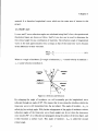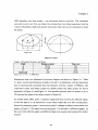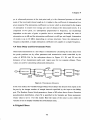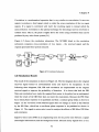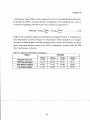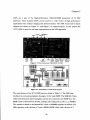
1
Durham E-Theses
Real-time digital signal processing system for normal
probe diraction technique
Zhang, Lei
How to cite:
Zhang, Lei (2006)
Real-time digital signal processing system for normal probe diraction technique, Durham
theses, Durham University. Available at Durham E-Theses Online: http://etheses.dur.ac.uk/2843/
Use policy
The full-text may be used and/or reproduced, and given to third parties in any format or medium, without prior permission or
charge, for personal research or study, educational, or not-for-prot purposes provided that:
• a full bibliographic reference is made to the original source
•
a link is made to the metadata record in Durham E-Theses
• the full-text is not changed in any way
The full-text must not be sold in any format or medium without the formal permission of the copyright holders.
Please consult the full Durham E-Theses policy for further details.
Academic Support Oce, Durham University, University Oce, Old Elvet, Durham DH1 3HP
e-mail: [email protected] Tel: +44 0191 334 6107
http://etheses.dur.ac.uk
Real-Time Digital Signal Processing
System for Normal Probe Diffraction
Technique
Lei Zhang
The copyright of this thesis rests with the
author or the university to which it was
submitted. No quoUtion from It, or
Information derived from it may be published
without the prior written consent of the author
or university, and any Information derived
from it should be acknowledged.
2006
Thesis for the Degree of Master of Science
School of Engineering
University of Durham
0 1 JUN lOOi
ABSTRACT
Ultrasonic systems are widely used in many fields of non-destructive testing. The
increasing requirement for high quality steel product stirs the improvement of both
ultrasonic instruments and testing methods. The thesis indicates the basics of ultrasonic
testing and Digital Signal Processing (DSP) technology for the development of an
ultrasonic system.
The aim of this project was to apply a new ultrasonic testing method - the Normal Probe
Diffraction method to course grained steel in real-time and investigate whether the
potential of probability of detection (POD) has been improved. The theories and
corresponding experiment set-up of pulse-echo method, TOFD and NPD method are
explained and demonstrated separately. A comparison of these methods shows different
contributions made by these methods using different types of algorithms and signals.
Non-real-time experiments were carried out on a V I calibration block using an USPC
3100 ultrasonic testing card to implement pulse-echo and NPD method respectively.
The experiments and algorithm were simulated and demonstrated in Matlab.
A low frequency Single-transmitter-multi-receiver ultrasonic system was designed and
built with a digital development board and an analogue daughter card to transmit or
receive signals asynchronously. A high frequency high voltage amplifier was designed
to drive the ultrasonic probes. A Madab simulation system built with Simulink indicates
that the Signal to Noise Ratio (SNR) can be improved with an increment of up to 3dB
theoretically based on the simulation results using DSP techniques. The DSP system
hardware and software was investigated and a real-time DSP hardware system was
supposed to be built to implement the high frequency system using a rapid code
generated system based on Matlab Simulink model and the method was presented.
However, extra effort needs to be taken to program the hardware using a low-level
computer language to make the system work stably and efficiently.
Contents
Abstract
I
Content
11
List of Figures
VI
List of Tables
VII
Declarations
VIII
Statement of Copyright
IX
Acknowledgements
X
CHAPTER 1
1
Introduction
1.1 Ultrasonic Testing Fundamentals
2
1.1.1 Ultrasonic Waves
1.1.2 Longitudinal and Transverse Waves
1.1.3 Mode Conversion
1.1.5 Sound Field
1.1.6 Acoustic Impedance
1.1.7 Probability of Detection
1.2 Ultrasonic Testing in Industry fields
1.2.1 Ultrasonic Testing Application in Steel Industry
1.2.2 Steel products, Continuous Casting and Rolling
1.2.3 Inclusions of Steel Billet
1.2.4 Current Ultrasonic Testing System
1.2.5 Single Transmitter Multi Receivers System
1.3 Previous Research
1.4 Project Aims
3
4
4
6
7
8
8
8
9
10
11
13
13
15
CHAPTER 2
17
Ultrasonic Testing
2.1 Ultrasonic Transducers
2.1.1 Transducer Parameters
2.1.1.1 Resolution and Sensitivity
2.1.1.2 Impedance
2.1.1.3 Frequency
2.1.2 Transducer catalogue
2.1.2.1 Straight-Beam Probe
2.1.2.2 Angle-Beam Probe
2.1.2.3 Twin-crystal Probe
2.1.2.4 Delay-line Probe
2.1.3 Transducer for Steel Inspection
2.2 Scan Types
18
18
18
18
19
19
20
21
21
21
21
22
U
2.2.1 A-scan
2.2.2 B-scan
2.2.3 C-scan
2.3 Test Methods
2.3.1 Pulse-echo Method
2.3.2 TOFD Method
2.3.2.1 Reflection and Diffraction
2.3.2.2 TOFD Technique
2.3.2.3 Defect Location and Sizing
2.4 Normal Probe Diffraction Technique
2.4.1 Experiment Equipments
2.4.1.1 Socomate USPC 3100 PC based ultrasonic flaw detector
2.4.1.2 Hewlett Packard M i n i u m oscilloscope
2.4.1.3 V I Calibration Block
2.4.1.4 Ultrasonic couplant Gel (Ultragel I I from Diagnostic Sonar Ltd)
2.4.2 Experimental Setup
2.4.3 Experiments with V I calibration
2.4.4 Experiment Conclusion
2.5 PC-Based Ultrasonic Test System
2.5.1 Assembling an Ultrasonic Test System
2.5.1.1 Pulser/Receiver
2.5.1.2 Ultrasonic Transducer
2.5.1.3 Digitizer
2.5.1.4 Application software
2.5.1.5 Communication
2.5.2 Pulser/Receiver (P/R)
2.5.3 Digitiser
2.5.4 Switching
2.5.5 Application Software
2.6 Summary
22
22
23
23
23
24
24
25
26
27
27
27
28
28
28
29
29
32
32
32
33
33
33
33
33
33
34
35
36
37
CHAPTER 3
38
NPD Algorithm
3.1 NPD Mathematical Model
3.2 NPD Simulink Model
3.3 Matlab G U I for NPD
3.4 Summary
38
40
42
42
CHAPTER 4
44
System Simulation Model
4.1 Simulink Model
4.2 Signal Generation
4.3 Attenuation
4.4 Time Delay and Environment Noise
4.5 Digital Filters
..r
......^.7
4.5.1 HR Filter
4.5.2 FIR Filter
4.5.3 Correlation
4.6 Simulation Result
4.7 Summary
III
45
46
47
48
49
49
50
51
52
54
CHAPTER 5
DSP System Architecture
55
5.1 System Hardware
5.1.1 Texas Instruments TMS320C6713 DSK
5.1.1.1 C6713DSP Core
5.1.1.2 EDMA (Enhanced Direct Memory Access)
5.1.1.3 Timer
5.1.1.4 EMIF (External Memory Interface)
5.1.1.5 CPLD (Complex Programmable Logic Device)
5.1.1.6 SDRAM (Synchronous Dynamic Radom Access Memory)
5.1.1.7 Daughter Card Interfaces
5.1.1.8 McBSP (Multi-channel Buffered Serial Ports )
5.1.1.9 AIC23 Codec
5.1.1.10 JTAG (Joint Team Action Group)
5.1.2 Analogue Daughter card
5.1.2.1 FPGA
5.1.2.2 THS5661 D A C
5.1.2.3 THS1230 A D C
5.1.2.4 Digital I/O Connector
5.2 Development Tools
5.2.1 Code Composer Studio
5.2.2 DSP/BIOS
5.2.3 Software Libraries
5.2.4 Support for Daughterboard Interfaces
5.2.5 Matlab Tools
5.2.6 FPGA Configuration
5.2.6.1 Digital I/O Register
5.2.6.2 Digital I/O Control Register
5.2.6.3 Status register
5.2.6.4 Start register and Period register
5.2.6.5 A / D Clock Rate Register
5.2.6.6 D/A Clock Rate Register
5.3 Real-Time DSP Prototype
5.4 DSK Application Example
5.4.1 Description
5.4.2 Ping-Pong Buffering
5.4.3 EDMA Linked Transfers
5.4.4 DSP/BIOS Real-time Analysis and Schedule
5.5 Real-time Rapid Prototype Example
5.5.1 Simulink Model and RTDX Resuh
5.5.2 Board Support Blocks
5.5.3 From/To RTDX Block
5.6 Summary
55
55
58
58
59
59
60
60
61
61
62
62
63
63
64
64
65
65
65
66
67
68
68
69
70
70
70
71
71
71
71
73
74
75
76
76
78
78
79
80
80
CHAPTER 6
81
AED330 Daughter Card Experiments
6.1 Test Program Description
6.2 Test Program Source Files
6.2.1 AED_Main
81
83
83
IV
6.3
6.4
6.5
6.6
6.2.2 AED_DMS_EDMA
6.2.3 AED_330
6.2.4 6xlx_BRD
Daughter Card Clock Frequency Test
40 kHz Ultrasonic Transceiver Circuit
High Voltage High Frequency (HVHF) Amplifier
Summary
CHAPTER 7
Conclusion and Further Research
83
83
84
84
86
88
90
91
7.1 Conclusion
7.2 Further Research
91
92
References
94
Appendix
Published Papers
1. The Institute of Materials, Minerals and Mining Conference: Advances in on-line
instrumentation for materials characterisation in metals industry Conference,
2005,London,UK
"Normal Probe Diffraction - Improving the Capability of Industrial Ultrasonic Probe
Arrays" - L.Zhang, S.Johnstone, P.Snowdon(University of Durham), S.Dewey(STC,
Corns p l c U K )
2. To be published on The British Institute of Non-Destructive Testing (BINDT) 2005
Conference, September 2005, Harrogate, U K
"Real-Time DSP System for Normal Probe Diffraction Technique" - L.Zhang,
S.Johnstone, P.Snowdon, S.Dewey
V
Lists of Figures
Figure 1. 1 Reflection and Refraction
Figure 1. 2 Sound Field
Figure 1. 3 Relationship and size of probes
Figure 1. 4 The two banks of probes
Figure 1. 5 Divergence of Pulse/Echo Signal
Figure 1. 6 Normal Probe Diffraction Experiment Setup
Figure 1. 7 Comparison of Probability of Detection for NPD and Pulse-Echo
Figure 2. 1 5MHz Transducer Parameter Measurement
Figure 2. 2 Four Fundamental Transducer Types
Figure 2. 3 Block diagram: Pulse Echo Method
Figure 2. 4 Reflection and Diffraction
Figure 2. 5 TOFD wave paths
Figure 2. 6 TOFD A-scan Schematic
Figure 2. 7 (a) Pulse-echo A-scan form probe 1
Figure 2. 7 (b) Pulse-echo A-scan form probe 1
Figure 2. 7 (c) Pulse-echo A-scan form probe 1
Figure 2. 8 Transmitter-Receiver Mode Test Result
Figure 3. 1 Ellipse
Figure 3. 2 Double Probes NPD Scheme
Figure 3. 3 Triple Probes NPD Scheme
Figure 3. 4 NPD Algorithm Simulation Model
Figure 3. 5 Matlab NPD G U I
Figure 3. 6 NPD G U I Example
Figure 4. 1 Ultrasonic Detection System Simulink Model
Figure 4. 2 Transmission Subsystem
Figure 4. 3 IIR Butterworth Lowpass Filter
Figure 4. 4 FIR Kaiser Lowpass Filter
Figure 4. 5 Correlation Subsystem
Figure 4. 6 Simulation Result
Figure 5. 1 Taxes Instrument TMS320C6713 DSK
Figure 5. 2 TMS320C6713 DSK Block Diagram
Figure 5. 3 DSK Memory Map
Figure 5. 4 AED_330 Daughter Card Block Diagram
Figure 5. 5 A Rapid Real-Time DSP Prototype
Figure 5. 6 DSK Application Example Hardware Diagram
Figure 5. 7 Real-time analysis using DSP/BIOS
Figure 5. 8 CPU Load Graph
Figure 5. 9 Execution Graph
Figure 5.10 Simulink Real-time Model: Time-Domain Acoustic Noise Canceller
Figure 5.11 Waterfall Plot of Filter Parameters
Figure 6. 1 Test Program DAC_table
Figure 6-2 Receive C i r c u i t . . . . . . . . . . . . . . . . . . . . . . T T T T ^ . . ;
Figure 6. 3 Tx-Rx using 3 Periods Square Wave
Figure 6. 4 Tx-Rx using Half Period Sine Wave
Figure 6. 5 Custom Amplifier Circuit
Figure 6. 6 PSPICE Simulation Result
VI
5
7
12
12
13
14
15
19
20
23
24
25
26
29
30
30
32
39
40
40
41
42
43
46
48
50
51
52
54
56
56
58
63
72
74
76
77
77
79
79
85
87
88
88
89
89
List of Tables
Table
Table
Table
Table
Table
Table
Table
Table
Table
3.
3.
4.
5.
5.
5.
6.
6.
6.
1 Transmit Distance and Time
2 Propagation Angles
1 Signal-to-noise Ratio Comparison
1 TMS320C6713 DSK Features
2 CPLD Registers
3 FPGA Control Registers
1 Daughter Board Test Program Functions
2 PLL Multiplier Control Daughter Card Sampling Frequency
3 PLL Divider Control EMIF Frequency
VII
39
40
53
57
60
70
84
86
86
Declarations
The author confirms that this thesis conforms to the word length prescribed for the
degree to which it is submitted.
No part of the material offered in this thesis has been previously submitted by the author
for a degree in this or any other University.
vm
statement of Copyright
The copyright of this thesis rests with the author. No quotation from it should be
published without prior written consent and information derived from it should be
acknowledged.
IX
Acknowledgement
This project has been sponsored by Corus. I would like to thank Steve Dewey for all
helpful comments and stimulating discussions.
I especially want to thank my supervisor Dr Sherri Johnstone, for her continuous
support guides me to learn not only harder but smarter; her encouragement leads me to
be self-confident in chasing my gaol; her positive attitude and happy manner teach me
how to treat research as a hobby and an art, rather than a tedious work; her
consideration covers both my academic progress and my daily life, helps me to
overcome any homesick and loneliness in a foreign country and focus on my study.
I also want to thank Paul Snowden for his previous research and testing; Adam Cluett
for his detailed explanation with patience and a good humour; Tom Grocutt for sharing
his knowledge and experience introducing me to hardware programming; Ian
Hutchinson for providing all necessary equipments and everyone in the School of
Engineering who has contributed to such a good scientific and technology environment
and shared their knowledge impartially.
VIII
Acknowledgement
This project has been sponsored by Corns. I would like to thank Steve Dewey for all
helpful conmients and stimulating discussions.
I especially want to thank my supervisor Dr Sherri Johnstone, for her continuous
support guides me to learn not only harder but smarter; her encouragement leads me to
be self-confident in chasing my gaol; her positive attitude and happy manner teach me
how to treat research as a hobby and an art, rather than a tedious work; her
consideration covers both my academic progress and my daily life, helps me to
overcome any homesick and loneliness in a foreign country and focus on my study.
I also want to thank Paul Snowden for his previous research and testing; Adam Cluett
for his detailed explanation with patience and a good humour; Tom Grocutt for sharing
his knowledge and experience
introducing me to hardware programming; Ian
Hutchinson for providing all necessary equipments and everyone in the School of
Engineering who has contributed to such a good scientific and technology environment
and shared their knowledge impartially.
IX
Chapter 1
CHAPTER 1
Introduction
In the course of the casting process, a variety of internal discontinuities can occur in the
metal. The main defects that lie in the final steel product include inclusions, bubbles and
cracks, all of which can affect the quality of the steel product. Main body defects
excluding near-field defects can be detected using appropriate N D T (Non-destructive
Testing) methods.
In bloom and billet mills, traditional on-line pulse-echo defect detection systems exist,
in which each probe is sequentially used to produce a radio frequency pulse, which is
then reflected from the defect and detected by the same probe. The results of
experiments carried out in previous research successfully show that the conventional
method of ultrasonic billet inspection discards much information which could be used to
improve the test integrity and sensitivity. Extra information can be obtained about the
defect to increase the probability of detection (POD) i f the diffracted signal is also
collected by neighbouring probes.
A standard Single-Transmitter-Multi-Receiver
system was built to implement this. As this technique is similar to time-of-flight
diffraction (TOFD), but does not require angle beam probes, it is referred to as Normal
Probe Diffraction (NPD). The aim of this project was to build the necessary real-time
hardware for the implementation of the NPD technique, thus giving the possibility of
improved on-line defect detection. Furthermore, modem advances in electronic and
signal processing are applied to improve the signal to noise ratio.
In chapter 1, basic ultrasonic theory which is relevant to NPD is described. Although
metallurgy is not within the scope of this project, the desired ultrasonic testing system is
to be used in steel mill to test the quality of products. Therefore, a brief outline of the
steel manufacture process is also included to assist in the understanding of some of the
potential problems within the manufacture of steel and the formation of internal defects
that require the development of complex inspection techniques.
Chapter 1
Chapter 2 describes the equipment, such as probes, test methods and standard
representations of signals used in ultrasonic testing and then applies these to non-realtime tests using the NPD algorithm on both a V I caUbration block and an as-cast billet.
It was found that the signal to noise ratio in the billet was low due to the large grain size,
so a model of the system was created in Matlab Simulink. To implement this, an NPD
simulation model was first created. This is described in Chapter 3. Chapter 4 then
describes how it is incorporated into a model of the complete ultrasonic test system,
using simulated input data. The model is then used to investigate and design different
filtering techniques to improve the signal to noise ratio such that the probability of
detection can be increased.
The next stage of the project was to implement the NPD algorithm in real-time. A
TMS320C6713 DSK was chosen as the base hardware platform, together with a highspeed analogue daughter card. This hardware and the associated development tools are
decribed in Chapter 5, together with some application examples for illustration. The
Matlab Simulink real-time rapid prototying method is described, but was not used in
this project since it could not easily support the third party daughter card.
Finally, chapter 6 includes work carried out in applying the DSK and daughter card to
transmit and receive signals from ultrasonic transducers with the ultimate aim of
applying NPD in real-time. To test the basic principles, a 40 kHz system was
investigated in which analogue interfacing hardware was designed and implemented. A
high speed (MHz) high voltage amplifier was designed but not implemented during this
project.
1.1 Ultrasonic Testing Fundamentals
Ultrasonics refers to any study or application of ultrasonic waves covering a range of
frequencies between 18 kHz and 25 MHz, much higher than the human audible sound
waves. Ultrasonic waves are used in many applications including plastic welding,
medicine and NDT. Within NDT, ultrasonic waves give us the ability to "see through"
solid/opaque material and internal flaws without affecting the material in an adverse
manner.
Chapter 1
Ultrasonic Testing is more than 40 years old. From the very first examinations, using
ultrasonic oscillations for detection of flaws in different materials, it has become a
classical test method based on measurements with due regard to all the important
influencing factors. Today it is expected that ultrasonic testing, supported by great
advances in instrument technology, give reproducible test results within narrow
tolerances. This assumes exact knowledge of the influencing factors and the ability to
apply these in the testing technology. Not all influences have to be seriously regarded
by the operator. In many cases some of the influences can be neglected without
exceeding the permitted measurement tolerances. Due to this, the test sequence is
simplified and the testing time reduced. Despite this, the future belongs to the UT
engineer who continuously endeavours to keep his knowledge at the latest state of the
art and the well designed automatic testing system which can carry out the task
efficiently.
1.1.1 Ultrasonic Waves
Ultrasonic waves are transmitted by high fi-equency particle vibrations. The ultrasonic
principle is based on the fact that solid materials are good conductors of sound waves,
whereby the waves are not only reflected at the interfaces but also by internal defects
such as inclusions. When an ultrasonic wave is transmitted in homogenous solid
material, the directed energy in it is reflected by boundaries between materials as well
as by any cracks or voids in the object. The reflected waves caused by internal defects
can be compared to the reflected waves from the external surfaces, enabling the size and
severity of internal defects to be identified.
The following relationship between frequency/fM//zj, wave length A (mm), and sound
velocity, c(km/s) is valid for all types of wave.
c = f*>.
(1.1)
Acoustic velocity is dependant on the material of propagation, and in general, is
constant for any frequency and wavelength.
This function indicates that ultrasonic
waves, which are mainly used in a frequency range between about 0.5 MHz and 25
MHz, have wave lengths in mm. With lower frequencies, the interaction effect of the
waves with internal flaws would be so small that detection becomes questionable.
Chapter 1
1.L2 Longitudinal and Transverse Waves
Two predominant types of waves, or wave modes, are generated within a material with
ultrasonic waves: longitudinal and transverse. Longitudinal waves compress and
decompress the material in the direction of motion, much like sound waves in air.
Transverse waves vibrate particles at right angles compared to the motion of the
ultrasonic wave. The velocity of transverse waves through a material is approximately
half that of the longitudinal waves. The angle in which the ultrasonic wave enters the
material determines whether longitudinal, transverse, or both waves are produced.
The mode of the wave affects the velocity, in that longitudinal waves have greater
velocity than transverse waves. The velocities of the sound waves are calculated from
the elastic constants of the material concerned, that is:
Modulus of elasticity E (measured in N/m^)
Density p in kg/m^
Poisson's ratio u
for longitudinal waves:
E
\-u
/>(l + M)(l-2«)
(1.2)
for transverse waves:
(1.3)
c, =
1.1.3 Mode Conversion
Ultrasonic beam refraction and mode conversion occur when an ultrasonic wave passes
from one medium to another. Refraction and mode conversion occur because of the
change in L-wave velocity as it passes the boundary from one medium to another. The
higher the difference in the velocity of sounds between two materials, the larger the
resulting angle of refraction. L-waves and T-waves have different angles of refraction
because they have dissimilar velocities within the same material.
The oscillaUons of longitudinal waves can be described by_ compression
and
decompression of the atoms propagating through the material (gas, liquid and solid).
Transverse waves only occur in solid materials never in liquids or gases because these
do not have a transverse modulus and therefore do not affect any transverse forces. In
addition to this, they propagate much slower than longitudinal waves in the same
4
Chapter 1
material. It is therefore longitudinal waves which are the main area of interest in this
project.
1.1.4 Snell's Law
L-wave and T-wave refraction angles are calculated using Snell's Law, the equation and
illustration figure are shown as follow. Snell's Law also can be used to determine the
first critical angle for any combination of materials. The refraction angle of longitudinal
waves is for steel approximately twice as large as that of the transverse waves because
of the difference of their velocities.
sma Si
sinP c^
(4.1)
Where a = angle of incidence, P = angle of refraction, c, = sound velocity in medium 1
Cj = sound velocity in medium 2.
T.
/
Inoomlng
\
1
1
/ //
/
/L
reflected
wave
meduinl
rmdl Lin Z
refrudBd
wave
Figure 1.1 Reflection and Refraction
By enlarging the angle of incidence, we will eventually get the longitudinal wave
refracted through an angle of 90°. This means that it runs along the interface whilst the
transverse wave is still transmitted into the test object. The angle of incident - a^L is
called the first critical angle. With further enlargement of the angle of incidence various
refraction angles of the transverse wave (beam angle) can be set when the transverse
wave reaches 90
it is refracted and propagates along the surface of the test object, and
it then becomes a surface wave. This angle of incident critical angle.
5
is called the second
Chapter 1
1.1.5 Sound Field
The ultrasonic waves only cover a certain section of the test object depending on the
certain directivity of the probe. The area effective for the ultrasonic test is called the
sound beam which is characteristic for the applied probe and material in which sound
waves propagate. A sound beam can be roughly divided into a convergent (focusing)
area, the near-field, and a divergent (spreading) part, the far field. The near field is the
region in an ultrasonic beam that is subject to variations of intensity due to diffraction
effects. It extends from the source of radiation to a point just short of the far field. The
length N of the near-field and the divergence angle is dependent on the diameter of the
element and the wave length of the ultrasound in the tested material.
(1.5)
The ultrasonic field is cylindrical from the face of the transducer to the end of the near
field[l]. In the far field the beam diverges conically with the apex at the centre of the
transducer face. The sound pressure disperses according to the inverse square law,
which is when the intensity is inversely proportional to the square of the distance. In
the far field the angle of divergence for the extreme width of the beam is given by[2]
Y
sin -i2 = k- ^ D
(1.6)
Where ^dB = constant based on stated dB drop from centre maximum. Values of ^dB
vary for the dB drop that is to be determined:
=0.37 when dB=3, ^dB =0.70 when
dB=6, '^dB = 0.87 when dB=20. Both the near field and beam angle are shown in Figure
1.2.
Chapter 1
N = n w f i « l d Iwigth
near (laid
teffsld
Figure 1. 2 Sound Field
1.1.6 Acoustic Impedance
When performing ultrasonic testing, it is important to understand how effectively
ultrasonic waves pass from one medium to another. Generally, when an ultrasonic wave
propagates from one medium into another, energy is partially reflected and partially
transmitted. The relationship in this phenomenon is described by acoustical impedance
and the acoustical impedance ratio.
Z = pV.
(1.7)
where Z is the acoustical impedance, p is the density of the sound medium and V is the
velocity of sound through medium.
For reference, air has low acoustical impedance, water has higher impedance than air,
and steel has higher impedance than water. The acoustical impedance ratio is the
impedance of the second material divided by the first. The higher the ratio, the more
energy is reflected. For example, when ultrasonic waves are passed from water to steel,
the acoustical impedance is approximately 20 to 1; whereas, when ultrasonic waves arepassed from air to steel, the acoustical impedance is approximately 100,000 to 1.
Almost 100% of the ultrasonic energy will be reflected when passing ultrasonic waves
Chapter 1
from air to a solid such as steel, making air a very poor ultrasonic couplant. That is
reason that the couplant gel is used in this project.
1.1.7 Probability of Detection
Probability of Detection (POD) is a term that describes the reliability of inspection
techniques. Two main elements affect POD; the technique and the human factor.
Broadly speaking the inspection reliability is defined as the probability of not
overlooking an existing defect (probability of detection, POD) and correct sizing the
defect. However simple this definition may appear, it encompasses many complex
issues ranging from the specification of the nature of defects to influencing factors
related with the inspection instrumentation, product nature, the involved human factor
and the available expertise for inspection data processing and assessing.
1.2 Ultrasonic Testing in Industry Helds
Among many UT methods developed for the detection of the steel defects, ultrasonic
testing has commonly and long been used in the industry fields. Tasks of ultrasonic
testing system include detection, location, evaluation and diagnosis of discontinuities.
The term "discontinuity" is defined as being an "irregularity in the test object which is
suspected as being a flaw". In reality, only after location, evaluation and diagnosis has
been made, can it be determined whether or not there is a flaw which effects the purpose
of the test object. The term "discontinuity" is therefore always used as long as it is not
certain whether it concerns a flaw which means a non-permissible irregularity[3].
1.2.1 Ultrasonic Testing Application in Steel Industry
Ultrasonic testing has been used for many applications, among which, steel production
and the manufacture of rods, tubes, and plates are ranked high for their importance and
advance. In some cases, in order to detect the internal and surface-breaking defects
without affecting the strength and integrity of the tested product and to guarantee that
the test results can meset specific standards, UT turns out to be one of the best choices
since it can fulfil these requirements easily Nowadays, the automated modem mills and
their high production speed demand for fast testing system capable for high pulse
repetition and real-time data processing. UT in this field operates ultrasonic probes
close to the surface of the testing products and uses complex mechanical system to
8
Chapter 1
handle the geometry, size and movement of the products under inspection. Ultrasound
lamb waves provide a reliable test for tube inspection without the need of rotation and
use relatively lowerfrequency.The lamb wave or guided wave is an interesting topic in
modem UT and worth of further study in the steel industrial. It is considered that the
real-time system discussed in this paper can also be amended and implemented with the
guided waves. This requires further research of the present test method using guided
waves. The strucmre of castings can highly attenuate the power of ultrasound, makes
UT methods less effective. However, this deficiency can be compensated by increase
the testing frequency and the output voltage of the pulse. 5MHz is chosen for this
project to get a relatively high resolution within reasonable amplitude attenuation.
1.2.2 Steel products, Continuous Casting and Rolling
In the past, molten steel used to be poured (teemed) into a large mould where it would
be allowed to cool and solidify to form an ingot. The ingot was then put into an oven
called a soaking pit, where it would be gently heated to the correct and uniform
temperature. This red hot ingot would then be rolled in primary mills, in the first stage
of its transformation into a usable steel product, into one of three forms of semi-finished
product: a slab (a long, thick, flat piece of steel, with a rectangular cross-section), a
bloom (a long piece of steel with a square cross-section) or a billet (like a bloom, but
with smaller cross-section).
In the UK, the continuous casting process has substituted the ingot route and become
dominant, while the ingot route may still be the most suitable way of producing the
required steel under certain circumstances.. For the continuous casting process, firsdy,
molten steel is poured into a reservoir at the top of the continuous casting machine. The
outer shell of the molten steel is then solidified by a water cooled mould. After this, the
steel is shaped by a series of rolls and fully solidified by water sprays at the same time.
The last step of this continuous process is to cut the steel to the required length to form
the final products like slabs, blooms and billets.
"Rolling is to reduce the thickness of a material by passing it between two rolls. Itis a
very popular forming process. It is divided into hot-rolling and cold-rolling according to
operating methods. Hot-rolling is mainly used for larger amounts of deformation and
cold-rolling is applied to optimise the mechanical properties and surface finish.
Chapter 1
Corns, formerly the British Steel Company, is one of the typical steel manufacturers in
the UK processing and distributing metal products such as steel bar and steel billet.
Scunthorpe Bloom and Billet Mill is part of the main Corns site in North East UK. The
mill produces various types of steel in billets that are widely used in industry; the
section of material of interest, for this project, a square section steel of sections ranging
from 76mm x 76mm down to 36mm x 36mm. Corns employs several different methods
of defect detection, which is dependant upon the positioning of the defect, i.e. surface,
sub-surface and core defects. The remit of the project is to investigate the core section
of the hot-rolled billet with a coarse grain structure using ultrasonic techniques.
A coarse grain structure metal contains fewer grains than a fine grain metal. A fine
grained metal is therefore harder than a coarse grained metal. The coarse grain structure
of steel product can scatter the pulse wave sent into the steel sample and form the
randomly distributed background noise disturbing the recognition of the defect
echoes[4]. Sometimes, grain refining agents are added to the molten metal before it is
cast to provide nuclei around which grains can grow. This will tend to produce a finer
grained material which is harder than it would have been with fewer grains.
An initial Eddy current inspection of the material (for surface breading cracks) is done
prior to the steel leaving the mill. The steel is then transferred in billet form to the
finishing mill. At the finishing mill it is reheated to 1200°C and rolled down to the final
size required of between 30-75mm. The ultrasonic inspection process takes place after
the material has been hot rolled down to the final size and cooled. The evaluation of the
ultrasonic signals is carried out with multi-channel electronics[5]. The coarse grain
structure of the as-cast bloom causes high attenuation of ultrasound[6]; it is more
practical therefore to inspect the steel post hot rolling. This process of working the steel
also improves the quality of the steel by refining its crystalline structure and making the
metal harder and tougher.
1.2.3 Inclusions of Steel Billet
At the Primaiy Mill the molten steel is continuously "cast as a 400mm square bloom. A
bloom is a bar of steel prepared for rolling. The casting process during which the
refi-actory shrouds cover the vessel and pore to prevent atmospheric exposure is the
main cause of inclusions being formed in the molten steel [7][8].Inclusions are small
10
Chapter 1
patches of impurities such as non metallic elements (e.g. carbon); or their oxides,
sulphides which are mixed into steel. These can be either something quite simple in
nature containing just one component or very often a much more complex multicomponent construction. In addition to chemistry, inclusions are characterised by their
size and shape[9] ; inclusions can be angular, globular or highly elongated. They usually
have to be removed from the steel in order for it to have good structural and mechanical
properties. Inclusions can have a major impact on the processing characteristics of steel,
and also the final in-service physical properties of the steel. The hot rolling process
elongates and concentrates these inclusions to the core of the billet, making the defect in
a billet rolled down from a bloom different from that of a direct cast billet.
There are two classes of inclusions which are dependent on elongation during hot
rolling:
•
Non-deformable inclusions - such inclusions are hard at rolling temperatures and
maintain their original shape as the steel is deformed.
•
Deformable inclusions - such species are soft at steel rolling temperatures and
deform and elongate as the steel is rolled.
1.2.4 Current Ultrasonic Testing System
Scunthorpe Billet Mill uses an immersion ultrasonic inspection system to detect defects,
cracks, and inclusions etc. within the core area of the material. The immersion system
has a stationary multi-probe array of eight 3/8 inch diameter piezoelectric transducers,
arranged at normal incidence to the material. Figure 1.3 shows the layout of the probes
in relation to each other. The piezoelectric transducers create a receive ultrasound to
convert energy between mechanical and electrical forms. The probes are set overlapping
so that no part of the material is left un-inspected. The ultrasonic system currently in use
is shown in Figure 1.4.
11
Chapter 1
Figure 1. 3 Relationship and size of probes
Figure 1. 4 The two banks of probes
Each probe works independently in a pulse echo mode. That is, the transducer that
transmits the signal also receives that signal. The probes are held at a distance of 70mm
from the material. This is to alleviate the possibility that they will be struck by the front
end of the moving bar, remove the complications involved with the near field of the
probe, and will be in the correct alignment to optimise the quality of the signals
achieved from the product. A high pulse repetition rate leads to full coverage of the
area to be inspected and the system is capable of detecting a 2mm defect because a
smaller wavelength can increase the testing precision.
When the front end of the bar has passed beyond the inspection probes, the inspection
system is "enabled'. This results in a short length of bar at the extreme front end which
has not been inspected (50mm - 100mm typically); this is known as "front end loss".
There is, therefore, an untested region at the ends of the bar, which is necessary to
suppress the alarm output from the inspection system, caused by distorted signals which
occur when probes pick up the abrupt edge of the bar end.
If any defects are
encountered by the inspection system, fixed paint jets at a position beyond the actual
Inspection Zone will subsequently mark the defective regions.
The inspection is
terminated prior to the tail end of the bar passing over the inspection probes and again
suppressing the alarm output similar the front end. This again results in an undetected
region at the tail end of the bar length known as back end loss. Bars, for which the line
control logic has been alerted to the defective nature of the product, are tracked through
the line and subsequently sorted into good or defective groups. The defective bars are
then manually re-inspected to qualify and define the nature of the defect.
12
Chapter 1
1.2.5 Single Transmitter Multi Receivers System
The above system can be amended to process the received transmission using several of
the probes. That is a single transmitter with multiple receivers. This idea is viable
because of the divergence of the ultrasonic wave as it is transmitted.
When an
ultrasonic probe is fired, the pulse of ultrasound is transmitted through the water
coupling into the steel billet, and is reflected off the back wall of the steel (pulse/echo).
Figure 1.5 shows the beam diverges when transmitting. The signal is received back at
the probe is only a small proportion of the total reflected signals.
Transmitted
Signal
Reflected
Signal
60mm X 60mm
steel billit
Figure 1. 5 Divergence of Pulse/Echo Signal
The remit of the project is to investigate and develop the latent potential within the
present system. The belief is that the system is not being used to its full potential in that
only one probe is in use at any time. If more than one or all probes could be used
simultaneously, the system would have greater efficiency. This could lead theoretically
to a faster throughput of material or a greater sensitivity of defect detection, and higher
reliability of defect detection.
1.3 Previous Research
The previous research has investigated the potential within a current multi-probe
ultrasonic detection system installed at a steel mill. Extensive laboratory experiments
were carried out using the transducer array geometry, to extract additional information
from passive probes. The apparatus was set up as shown in Figure 1.6.
13
Chapter 1
22.50
22,50
Probe 1
Probes
Probe 2
•2mm N o t c h ( d e f e c t )
Figure 1. 6 Normal Probe Diffraction Experiment Setup
Figure 1.7 shows the increase of detection ability using the standard single-probe-multireceiver (SPMR) system over the conventional single-probe-single-receiver (SPSR)
system. It shows that the NPD system starts detecting the defect at a lateral distance of
41mm from the defect whereas the pulse-echo probe needs to be within a range of
15mm. The physical principle behind this system uses diffracted waves from the edge
of the defects and thus it is particularly effective for the increased detection and sizing
of centre-line defects. This technique is defined as Normal Probe Diffraction (NPD),
which has been successfully applied offline on a V I calibration block and a single billet,
but has not yet been applied for real-time control.
Experiments show that the defect detection range can be increased by collecting the
diffracted pulse on all the neighbouring probes. This is due to the defect being detected
several times per pulse. The research project involves developing a real-time laboratory
based prototype which can detect defects using two methods: the standard single probe
pulse echo technique and NPD, and testing the system on a V I calibration block and a
steel billet. In this project, the transmitting and receiving electronics are developed to
enable the NPD technique to be applied in real-time[10].
14
Chapter 1
Probability of Detection
-P/E
NPD
I -
45 42 39 36
33 X
27 24 21
ie
15
12
9
B
3
D
Distance from Defect (mm)
Figure 1. 7 Comparison of Probability of Detection for NfPD and Pulse-Echo
A coarse grain steel billet was tested based on the previous research discussed above. A
slice was cut as a pseudo back wall and a 2mm diameter hole was drilled as a pseudo
defect, both were 30mm from the upper surface. The slice could be tested while the hole
could not. Therefore, further research has been made in both the field of ultrasonic
testing and the digital signal processing technique to improve the probability of
detection.
1.4 Project Aims
•
Study the principles of ultrasonic defect detection including NPD
•
Investigate large grain steel billets using off-line NPD, found needed better S/N
ratio
•
Simulate the NPD system to investigate methods of improving S/N ratio and aid
in finding the defect
•
Use simulation as a base for the real-time DSP rapid prototyping system.
Real-time DSP System
In this project, a rapid Digital Signal Processing (DSP) prototype for the necessary realtime system is modelled and simulated to implement the NPD technique.
TMSC320C6713 DSK and AED_330 analog expansion daughter card were used to
process digital signals in real-time to gain a fast Digital to Analogue conversion speed
15
Chapter 1
for the desired high frequency pulse signal. The desired real-time system was to help
increase the probability of detection of defects in steel billets and produce a low-cost
system solution for ultrasonic billet inspection in the steel industry.
A good real-time implementation should be reliable, low power consuming, compact
and always runs in real-time[l 1]. Sufficient amount of instructions per second and quick
enough transport speed must be considered and calculated during the design procedure
to meet the requirement of short delays between inputs and outputs in real-time
implementation.
This system uses general purpose digital signal processors for solving problems in realtime, and particularly focuses on using the Texas Instruments (TI) TMSC6713 DSK
(Digital Signal Processing Starter Kit) with the C6713 kernel floating point processor to
implement programs written in assembly and C. The T l C6713 DSK is for general realtime signal processing applications. The main applications taking place in this project
are digital filter design using different DSP algorithms. These filters are characterized
and applied on the received data. T I Hardware/software development tools (Code
Composer Studio and DSP/BIOS) provide 1/0 channels for data exchange with Matlab
in real-time.
System testing uses MATLAB and Simulink including several toolboxes. The
MATLAB Embedded Target for T I C6000 DSP enables the rapid prototyping of realtime software for C6713 floating-point processor and generates efficient code for the
processor directiy from a Simulink model using MATLAB Real-Time Workshop. The
generated code is readable and editable, and the code profiler identifies regions of
generated code that may benefit from manual optimization. The Embedded Target for
Tl C6000 DSP automates the creation of Link for the Code Composer Studio project,
provides board support for the C6713 DSK board, invokes Link for Code Composer
Studio to create a DSP executable and downloads the executable to the DSK board for
real-time algorithm evaluation. It also employs the link to enable interactive debugging
and systematic testing of the DSP programs
16
Chapter 2
CHAPTER
2
Ultrasonic Testing
This chapter gives an overview of the basics of ultrasonic testing techniques,
classification of ultrasonic probes and their applications, the main defect that occurs in
the steel industry and the existing ultrasonic testing system and method used to detect
them.
Ultrasonic detection techniques have developed at a tremendous rate to fulfil the
requirement for high quality defect free material in many industrial and research
applications. The basic method is the Conventional Pulse-Echo Method. As dictated by
its name, the Pulse-Echo method use an array of probes in which each probe pulses and
receives sequentially. This method was replaced gradually by some new techniques
based on Time-of-Flight Diffraction (TOfD), because these new methods collect extra
information from diffracted signal which was previously discarded by the pulse-echo
detection.
When Ultrasound is incident at a linear discontinuity such as a crack, diffi-action takes
place at its extremities in addition to the normal reflected wave. This diffracted energy
is emitted over a wide angular range and is assumed to originate at the extremities of the
crack. This is in marked contrast with conventional ultrasonic detection which relies on
the amount of energy reflected by discontinuities.
The TOFD technique, which is an off-line method, uses angled beam probes to pick up
the diffracted signal, while the NPD technique can get the same result with normal
probes by using multi-receivers, thus enabling the method to be implemented in realtime on a production line.
Both the TOFD"aird NPD"ultfasonic~techniqueT-elies~^^^
"diffraction of ultrasonic
energies from 'comers' and 'ends' of internal structures in a component under test. This
is in contrast to the conventional pulse echo method which relies on directly reflected
signals from internal structures and only can test the depth of the defect, while the
17
Chapter 2
former two methods can detect the defect in 2D and could be improved to 3D detection
by using an array of probes.
2.1 Ultrasonic Transducers
Ultrasonic transducers are built around piezoelectric ceramics that vibrate at ultrasonic
frequencies when a voltage is applied, and generate voltages when vibrated. The
transducer is one of the most critical components of any ultrasonic system. A literature
search has been carried out to investigate the correlation between transducer properties,
defect size and depths, and the signal to noise ratio during ultrasonic inspection of steel
with coarse grain structure. However practical test have been made to select the
appropriate transducer for the application.
2.1.1 Transducer Parameters
2.1.1.1 Resolution and Sensitivity
Ultrasonic transducers perform according to two main parameters: resolution and
sensitivity. The resolution of a particular transducer is denoted by its ability to discern
between two discontinuities that are on top of one another. A transducer with sufficient
resolution will stop ringing, or vibrating, from the first discontinuity before receiving
the echo from the second discontinuity. If the ceramic does not stop ringing before the
second echo is received, the second echo is masked from the test system. Sensitivity of
an ultrasonic transducer refers to the ability to detect small discontinuities. Reference
blocks with standard sized defects are used to gauge the sensitivity of a particular
transducer.
2.1.1.2 Impedance
Impedance (Z) is the resistance of a circuit to alternating current, such as an audio
signal. Technically, impedance is the total opposition (including resistance and
reactance) that a circuit has to passing alternating current. A high impedance circuit
tends to have high voltage and low current. A low impedance circuit tends to have
relatively low voltage and high current.
18
Chapter 2
Figure 2.1 shows that the measured impedance of the transducer at the frequency of
5MHz is 7.5 ohm (phase 10.7°).
H : 121
B: 8 z
SCfiLt
SCfiLE
2 0 n / d . l ¥ REF
2 0 " / d i V REF
60 Q
0 *
7 . 5 0 8 0 1 ,0 ,
s.BBse/'qgai MHz
CMP
:
—
VfIC
START 1 nHz
T't"'^
2MHz
3MHz
4MHz
5MHz
.V/IOG
STOP IB JlHz
Figure 2.1 5MHz Transducer Parameter Measurement
2.1.1.3 Frequency
The frequency of the ultrasonic transducer is chosen based on several factors including
detectable defect size, depth of penetration, and grain size of the material. Materials
made up of fine grained material, such as metals, permit deep penetration by ultrasonic
waves of all frequencies. However, coarse grained materials, including many plastics,
scatter high frequency ultrasonic waves. The higher the frequency, the smaller defects
the system will detect, but the depth of penetration decreases. So a trade-off has to be
made between the required sensitivity and depth of penetration.
2.1.2 Transducer catalogue
Ultrasonic transducers generate and detect ultrasonic waves. Piezoelectric ceramics
within ultrasonic transducers are excited by an extremely short electrical discharge,
typically between 50 and 1000 Volts to produce the ultrasonic wave. The same element
19
Chapter 2
on the other hand generates an electrical signal when it receives an ultiasonic signal thus
causing it to oscillate. The probe is coupled to the surface of the test object with a liquid
or coupling paste so that the sound waves from the probe are able to be transmitted into
the test object.
Ultrasonic transducers work almost exclusively according to the piezoelectric effect and
are classified into four fundamental types: Straight beam transducers, Angle beam
transducers, Delay line transducers and Twin crystal transducers[12]. Transducers also
differ with respect to the size of the active piezoelectric elements, their frequency,
bandwidth and the basic design. The selection of bandwidth is essential for achieving
certain test results; a narrow bandwidth for highly sensitive testing, or broad banded for
high resolution testing.
a) Straight beam, direct contact
Piezoetecuiceemem ,/"
Proleciive la/er
./.
/
/
.
/
/
/
/
. / /
/
/
/
/
/
/
/
/
/
/
b) Angle
/
/
/
'
/
/
/
/
'
/
/
•
'
/
/
/
.'
y
c) TR
/ / / / / /
/
d) Delay line
'•^Wrtehhs layer
Dalai lin* .1
Figure 2.2 Four Fundamental Transducer Types
2.1.2.1 Straight-Beam Probe
Probes whose beams are normal to the surface are called straight-beam probes as shown
in Figure 2.2(a). Most standard straight-beam probes transmit and receive longitudinal
waves. There is a large selection of straight-beam probes in various sizes and range
fronrffequencies bf approximaitely 0:5 MHz"to"25"MHzrDistarices of over 10 inch can
be obtained thus enabling large test objects to be tested. The wide range enables
individual matching of probe characteristics to every test task, even under difficult
testing conditions.
20
Chapter 2
2.1.2.2 Angle-Beam Probe
Angle beam transducers are single element transducers used with a wedge to introduce a
refracted transverse wave or longitudinal wave into a test piece. A n angle-beam probe is
shown in Figure 2.2(b). Most standard angle-beam probes transmit and receive, due to
technical reasons. Angle-beam probes do not transmit longitudinal waves. Due to the
fact that steel is tested in most applications, the angle-beam probes are designed so that
suitable angles of incidence are produced in steel. Angle-beam probes do not have such
a wide selection as straight-beam probes. This is primarily due to the fact that high
frequency transverse waves in non-alloyed fine grain steels are subjected to high
attenuation. As the sound energy of the waves travels through the material it is so
strongly absorbed and scattered that only relatively small test objects can be tested with
sufficient sensitivity.
2.1.2.3 Twin-crystal Probe
A twin crystal probe is a single transducer containing two piezoelectric elements, one
for transmitting and one for receiving. The crystal assemblies are separated by some
form of an acoustic barrier (usually cork) in order to prevent cross noise. Figure 2.2 (c)
shows a Twin-crystal Probe.
2.1.2.4 Delay-line Probe
The construction of the Delay-line probe is shown in Figure 2.2(d). Basically it is a
straight beam probe with an additional delay-line made of plastics with low ultrasonic
absorption. The time delay avoids echoes from defects close to the surface appear
within the dead zones of the ultrasonic defect detector, which are caused by the high
voltage excitation pulses[3]. Dead zone refers to the non-testable area immediately
beneath the surface. Use of delay-line probes is a simple measure to have an excellent
near field resolution.
2.1.3 Transducer for Steel Inspection
The type of transducer used is dictated to by the conditions in which they are to operate.
In the inspection of steel, consideration must"be~given~tci~the' metallurgical structure;
grain type, size and distribution all influence the propagation of the ultrasonic sound
21
Chapter 2
beam. Large or directionally oriented grains tend to scatter and otherwise absorb the
ultrasonic energy, to a greater extent than fine, randomly oriented grains. The
combination of these two effects, that is scattering and absorption, is termed attenuation.
To minimise this attenuation it is therefore necessary to use a probe with the optimum
frequency for steel, generally between 2 and 5 MHz. The probe chosen for the project
was also used in water and therefore required a special immersion type transducer and
cables.
2.2 Scan Types
There are several ways to look at ultrasonic test data ranging from TOF to surface scan.
The most common scans are referred to as A-, B- and C-scans.
2.2.1 A-scan
The most primitive method to analyze the reflected ultrasonic signals is time-of-flight
(TOF) scan, or A-Scan, which displays voltage amplitude versus depth. The depth is
calculated by multiplying the speed of sound through the medium by the time of flight.
Defects that are closer to the ultrasonic transducer are received sooner than those further
away from the transducer. The x-axis on the A-scan is not typically units of time, but is
converted to distance. This conversion is accomplished by measuring, or looking up, the
speed of sound through the material that the ultrasonic wave is travelling and
performing the conversion. Although there are a few exceptions, the speed of sound
through a material is governed largely by the density and elasticity of the material. For
most materials, the nominal speed of sound within homogenous material is easy to
research and find.
2.2.2 B-scan
B-scan is a two dimensional graphical presentation, in rectangular coordinates, in which
the travel time of an ultrasonic pulse is represented as a displacement along one axis,
and transducer movement is represented as a displacement along the other axis.
-In other words, B-scan images-the-voltage peaks in the A-scan moving back-and-forth
over time. This movement is caused by the varying thickness of the test object as the
22
Chapter 2
transducer is moved over the surface. Put all of those A-scan images together and the
result is a B-scan.
2.2.3 C-scan
C-scan is also a two dimensional graphical presentation, in which the defect echoes are
displayed in a top view on the test surface. C-scans display x- and y-position, while the
colour represents depth.
2.3 Test Methods
There are two operating modes for ultrasonic probes, pulse-echo and throughtransmission. In pulse-echo mode, each ultrasonic transducer transmits a signal out and
receives the echo. The reflected ultrasonic waves vibrate the piezoelectric crystal within
the ultrasonic transducer and generate voltages that are measurable by data acquisition
hardware. In through-transmission mode, two ultrasonic transducers are used; one
transducer generates the pulse signal and the other receives the echo.
2.3.1 Pulse-echo Method
Sound reflections in the audio range are called echoes. The name of the method came
into being which is applied in most areas of application for material testing with
ultrasonics is the Pulse Echo Method as shown in Figure 2.3[13].
start signal
(pulse)
flnish signal
(echo)
stop
watch
Tnuismittei
probe
source transit path
transit tiine
measurement
work piece
Figure 2. 3 Block diagram: Pulse Echo Method
23
Chapter 2
The time measurement starts with the electrical transmission pulse, the initial pulse.
This is an extremely short electrical discharge which triggers a sound pulse at the probe
crystal. This pulse travels through the material and is reflected by a discontinuity or the
opposing wall and returns back to the probe. The received oscillations are converted
into an electrical pulse which stops the time measurement. The distance to the reflector
can now be instantly determined by the following formula:
c*t
s=—
(2.1)
Where s is the length of the sound path in mm, c is sound velocity in km/s and t is the
time of flight in ms.
The problem with the pulse-echo technique is that it is based on the assumption that
echoes come from planar features within normal angle of incidence to give a specular
reflection back to the transducer. Clearly it is quite rare for defects to be exactly normal
to the beam as would be required for a perfectly smooth large specular reflector.
2.3.2 T O F D Method
2.3.2.1 Reflection and Diffraction
When ultrasound is incident at linear discontinuity such as a crack, diffraction takes
place at its extremities in addition to the normal reflected wave. This diffracted energy
is emitted over a wide angular range and is assumed to originate at the extremities of the
defect. Figure 2.4 shows both reflection and diffraction of a crack. This is in marked
contrast with conventional pulse echo method, which relies on the amount of energy
reflected by defects.
1 = transmitted wave
2 = reflected wave
3 = through transmitted wave
^^/JJ
^
4 = diffracted wave at upper crack tip
5 = diffracted wave at lower crack tip
Figure 2. 4 Reflection and Diffraction
24
Chapter 2
2.3.2.2 T O F D Technique
The TOFD technique uses a single probe pair in a transmitter-receiver arrangement.
Usually longitudinal probes are applied with an angle of incidence range of 45° to 70°.
The received data consist of signals transmitted between transmitter and receiver and
diffracted signals from defects. In addition to energies diffracted by defects, the TOFD
method will also detect a surface wave travelling directly between the probes and also a
back wall echo from energies that reach the back of the tested object without
interference from defects. Because the technique relies on detection of the forward
scattered diffracted signals originating at the defect edges, precise measurement of
defect size, location, and orientation is possible, and inspection reliability improves.
Point reflectors are precisely determined by using geometric considerations, beam
angles, and the appropriate sound propagation velocity.
•2S-
Transmitter
Receiver
Inspection surface
Lateral wave
Transducer
beam profile
(scheroatic)
Crack
xP
Isotropic
material
Backwall
Figure 2. 5 T O F D wave paths
2S
= Distance between probes
a
= Length of defect
0
= Refracted beam angle in material
H
= Material thickness
d
= Depth of defect
25
Chapter 2
-a
mode
converted
pulse
Figure 2. 6 T O F D A-scan Schematic
2.3.2.3 Defect Location and Sizing
Location of the crack tips is determined from the time differences between the lateral
wave and the pulses that follow the paths;
Pl-^Pl
or
(2.2)
These paths correspond to t i (top of crack) and ta (crack bottom) respectively. Figure
2.5 shows the four wave paths and Figure 2.6 shows the detection of four main signals
and a mode converted signal from the top of the crack.
tL: the surface or lateral signal which travels along the surface of the component and has
the shortest arrival time
2S
(2.3)
ti: the top tip of the defect
2yls'+d'
t2: the bottom tip of the defect
26
(2.4)
Chapter 2
U =
(2.5,
tBW; the back-wall echo, which has the longest transit time
tfiw =
^
(2.6)
d=^y[c't;-4S'
(2.7)
a = ^^Ic'tl-4S'-d
(2.8)
Rearranging the equations,
Length of defect (a)
C is taken to be the velocity of the bulk compression wave.
Equation 2.7 and 2.8 are used generally in the analysis of TOED data and are thus of
basic importance. The assumption that the defect is positioned symmetrically between
the probes introduces an error but this can be arranged to have little effect on the
accuracy of the estimated defect depth[14]. By use of today's advanced computer
techniques it is possible to evaluate signals very rapidly. That makes it possible to
perform scans with a speed of hundreds of millimetres per second. In practice speed is
limited only by the mechanic.
2.4 Normal Probe Diffraction Technique
Normal Probe Diffraction (NPD) Technique firstly debuted in 2003 by Paul C.
Snowdon, Sherri Johnstone and Stephen Dewey[15]. Experiments were conducted to
investigate that the probability of detection can be increased by using passive normal
incidence transducers to pick up diffraction signal. On one hand, NPD technique makes
use of the diffraction signal previously discarded by the conventional pulse-echo
ultrasonic detection system for the on-line steel inspection. On the other hand,
compared to TOED, NPD does not require special beam-angle probes thus decreases the
cost of testing.
—
27
Chapter 2
2.4.1 Experiment Equipments
2.4.1.1 Socomate U S P C 3100 P C based ultrasonic flaw detector
The USPC is a Plug & Play windows based PC Card flaw detector with two transmit/
receive channel.
It is a real time DSP system for in-line ultrasonic inspection and is
supplied with the application software written in Labview. Various options are available
for A-Scan, B-Scan & C-Scan Acquisition.
2.4.1.2 Hewlett Packard Infinium oscilloscope
The 2-channel oscilloscope has a window-based graphical interface and an integrated
3.5" floppy disc drive for data transfer. The bandwidth of the oscilloscope is 500MHz.
The acquisition filter was set to a 16 average filter to improve the signal to noise ratio
and signal stability. This was the optimum setting for the oscilloscope because a greater
numerical average would affect the refresh rate and sample length at the chosen
sampling frequency of 50MHz. The 50MHz sampling frequency is above the Nyquist
sampling frequency to avoid signal aliasing problems[16]. The 5kHz system slowest
repeat rate was selected to be the pulse repetition frequency to facilitate signal decay
and reduce spurious echoes.
2.4.1.3 V I Calibration Block
The reference piece used for calibration is called the Calibration Block, or Standard
Calibration Block, i f the block used is standardized. The Standard Calibration Block 1,
also simply referred to as V I block (according to BS 2704 - A2), which is shown in
Figure 1.6, has a thickness x width x length of 25x 100x300mm and is made of lowalloyed fine grained steel so that it can be used for nearly all types of calibration when
similar steels are to be tested.
The 2 nun-wide notch, 85 mm from the inspection
surface was chosen as a pseudo defect.
2.4.1.4 Ultrasonic couplant Gel (Ultragel I I from Diagnostic Sonar Ltd)
Ultrasonic Couplant Gel is necessary because sound energy at the ultrasonic frequencies
typically used for non-destructive testing is not effectively transmitted through air. Even
an extremely thin air gap between the transducer and the test piece will prevent efficient
28
Chapter 2
sound energy transmission and make conventional testing impossible. The general
purpose propylene glycol based couplant used in these experiment was chosen because
it has good surface wetting properties, thus will not corrode or otherwise attack
materials, and it is easily washed off by water and chemically non-reactive and does not
evaporate quickly at room temperature. Propylene glycol has an acoustic impedance of
1.61X10^ gm - cm^ / sec which is close to that of 1.48 x 10^ gm - cm^ / sec for water.
2.4.2 Experimental Setup
The experiment equipments were set up as shown in Figure 1.6. Three straight-beam
probes placed in a linear arrangement, normal and in contact with the upper surface of
the V I standard calibration block. The probes were used in a single transmitter with
double receiver in alternate positions. Receiver probes were located at distances of 22.5
mm and 45 mm from the transmitter. This experimental setup was used to reveal the
clearest interpretation of the received reflection and diffraction signals.
2.4.3 Experiments with V I calibration
In experiments, each of the three probes was excited in turn using the USPC 3100 in Ascan pulse-echo mode. The received signals were displayed on the oscilloscope and
transferred digitally to the PC for further processing and analysis using M A T L A B . The
signal velocity measured using probe 1 in pulse-echo mode[17] within the V I block
is5900ms"'±l%.
6
-i
10
1
IS
!_
20
H
30
^6
TbneCiis)
Figure 2. 7 (a) Pulse-echo A-scan form probe 1
29
40
^
Chapter 2
26
27
2S
29
30
31
32
33
TlmeOia)
34
36
(b) Pulse-echo A-scan form probe 2
rtiDe(iu)
(c) Pulse-echo A-scan form probe 3
Figure 2.7 (a) (b) (c) shows the pulse-echo A-scans from probe 1, probe 2 and probe 3
respectively. The A-scans indicate that the 2mm notch is undetectable at probe 1 and
distinguishable at probe 2 at a 50dB gain. In the A-scan from probe 3, point 1 is the
notch, point 2 is the 91mm step back wall and point 3 is the 100 mm back wall. This
verifies that in the following transmitter-receiver mode experiment, the signals received
by two receivers are non-specula reflection or diffraction signals rather than directional
reflection signals.
Figure 2.8 (a) to (e) display the signal from the defect and first back wall echo as after
the back wall, it is impossible to distinguish between signals due to multiple internal
reflections. Each probe was excited in turn and the left two probes acted as passive^
receivers and acquired diffracted signal.
30
Chapter 2
0.015
0.04
0.010 A
0.03 .
0.02 •
0.005
1
E
0.000
0.01 A
0.00
I
A
^.01
H
-0.02 -0.010 H
-0.03 -
-0.015
29 31 33
T%n« (us)
35
-0.04
37
f
31
2&
33
0.04 1
0.03
0.03 •
0.02
0.02
1 0.01 •
a.
0.00 -
0.01
o.oo
1
-0.01 H
^.02 -
-0.03
-0.0327
29
31
33
37
35
-0.O4 •
25
37
'nma{U8)
(c) Transmitter-Probe 2/Receiver-Probe 1
fw
-0.01 •
-O.02
25
35
(b) Transmitter-Probe 3/Receiver-Probe 2
0.04
-0.04
27
rms(us}
(a) Transmitter-Probe 3/Receiver-Probe 1
i
25
27
29
31 33
HnM{us)
36
37
(d) Transmitter-Probe 2/Receiver-Probe 3
0.015 T
0.010
o
0.01
0.005
lU
% 0.00
0.000
-0.01
-O.006
-^.02
-0.010 4
-0.03
-0.015 ^
-0,04
25
27
2d 31 33
IftmCus)
36
-0.020
37
Mma(us)
(e) Transmitter-Probe 1/Receiver-Probe 2
(f) Transmitter-Probe 1/Receiver-Probe 3
Figure 2, 8 Transmitter-Receiver Mode Test Result
31
Chapter 2
2.4.4 Experiment Conclusion
The experiment results show that passive probes setup next to the transmitter can detect
the signals correspond to the shortest signal paths via defects that are outside the normal
detection range of the transmitting probe shown in Figure 1.6. The NPD technique was
therefore proved to be able to improve the potential of the POD within a static array
system. Three mechanisms were considered to explain the result of the experiments:
directional reflection, electromagnetic coupling and diffraction[10]. A PC based DSP
system and control software were to be designed and built based on this technique to
carry out ultrasonic testing in real-time in this project. The architecture of this system is
represented in chapter 3.
2.5 PC-Based Ultrasonic Test System
The performance of the system as a whole is of great importance. Variations in
instrument characteristics and settings as well as material properties and coupling
conditions play a major role in system performance. The hardware and software
components must interact effectively for even the simplest ultrasonic test system to
work properly. When assembling the custom ultrasonic test system, there are several
factors to consider for each component of the system, including how well the
components interact with one another. The Ultrasonic Transducer section describes each
component of the test system in detail as well as the important features required for
ultrasonic testing.
Several PC-based and external components make up each ultrasonic test system. Each
of
these components has a unique set of features and considerations. Some
considerations are limited to the component itself while others depend on the various
components in the system. The features/issues of these components are considered to
build the ultrasonic test system to implement the NPD algorithm.
2.5.1 Assembling an Ultrasonic Test System
Ultrasonic test systems can take several forms, but the most common for automated test
is immersion testing. The offline experiments carried out in previous research of this
project use an immersion tank filled with water to have good acoustical impedance
32
Chapter 2
matching between the couplant and the tested object and free range over the entire
surface of the object.
The test system uses one or more ultrasonic transducers, which are moved over the
surface of the tested object. As the transducer is moved over the surface, it is pulsed and
receives echoes from various surfaces. This process is repeated many times a second.
There are several pieces of the test system that must work together to get expected
results. The following list includes the steps, and the accompanying hardware and
software pieces, required to get one pulse and the subsequent echoes:
2.5.1.1 Pulser/Receiver
This device generates the high voltage pulse that is required by the ultrasonic transducer.
The analogue signal from the ultrasonic transducer is amplified and filtered before it is
sent back to the digitizer within the PC.
2.5.1.2 Ultrasonic Transducer
The transducer is pulsed, sending out an ultrasonic wave. The subsequent echoes
generate a voltage in the transducer, which is sent back to the pulser/receiver.
2.5.1.3 Digitizer
The waveform sent from the pulser/receiver is converted from voltage to bits using an
analogue-to-digital converter.
2.5.1.4 Application software
The user interacts with the application software to set up the test and presentation
parameters. Data from the digitizer is processed, analyzed, and presented according to
the user-defined parameters
2.5.1.5 Communication
The pulser/receiver operation parameters, such as pulse energy, pulse damping, and
bandpass_filterjng,:are_set._The_communication.path.is_typically R S - 2 3 2 _ O L U S B
2.5.2 Pulser/Receiver (P/R)
33
Chapter 2
These devices provide the high-voltage pulse required by the ultrasonic transducer as
well as signal conditioning before the analogue signal is passed to the digitizer. For use
within an automated test system, the P/R should be computer programmable via a
standard PC bus such as RS-232 or USB. The USPC 3100 flaw detector uses a RS-232
while the T I C6713DSK uses a USB port. The devices are typically programmed once
at the beginning of the test to set the pulse voltage level, pulse repetition frequency,
damping, band pass filtering settings, and several other parameters. After these
parameters are set, these devices are passive and do not send any information back to
the PC during operation. Digitizer and P/R must operate as one tightly-timed unit during
the test to ensure accuracy of results and brevity of test time.
2.5.3 Digitiser
This part of the test system converts the echo waveforms returned by the ultrasonic
transducer into digital information using an analogue-to-digital converter (ADC). Some
factors such as sample rate, bandwidth, vertical resolution, triggering features, memory,
and bus type need to be considered for digitiser selection.
For applications that require well-shaped waveforms in the time-domain, such as
research, a sample rate 10 times higher than the resonant frequency of the transducers is
desirable. In these applications, a transducer that has a resonant frequency of 5 MHz
requires 50 MHz to accurately represent the shape of the signal. In this project accurate
time-domain waveform is required, so 50MHz sample rate is used. However, for
applications that require less amplitude and echo-timing accuracy, 4-5 times the
resonant frequency is acceptable.
Vertical resolution establishes the minimum voltage step size within a voltage range.
16-bits is equivalent to 65,536 (2-^16) steps. When a 16-bit ADC is applied to a voltage
range of 0-1 Volts (AIC23 codec A D C of T I C6713 DSK board), the minimum voltage
step size is 15.3 |xV ( I V / 65,536). However, when a 12-bit ADC is applied to a voltage
range of 2V (THS1230 A D C on the AED daughter card), the minimum voltage step size
is 0.49 mV (2V / 4096). In ultrasonics, the voltage amplitude is proportional to the
amount of energy echoed by the discontinuity or defect. The front face and back wall of
the-tested object-generally-reflec^the-most-energy, while defects reflect much less; To
see the energy reflected from small flaws, the signal from the transducer must be
34
Chapter 2
amplified or the digitiser must have high resolution. Amplifying the signal to detect a
small defect can cause the front surface and back surface reflection voltages to swing
outside the voltage range of the digitizer. On the other hand, additional resolution
permits the user to zoom in on small defects and not distort main surface reflections at
the same time. High resolution also relaxes the amplification levels required by the P/R
component.
Flexibility of internal or external timing is essential for ultrasonic test applications. A
programmable trigger delay is also a useful feature for ultrasonic testing. In immersion
testing, the ultrasonic wave must travel through a significant distance of water before
arriving at the tested object. I f this distance is known, a trigger delay can be
implemented to minimise the amount unnecessary data that is recorded and stored.
Because of the high frequencies associated with ultrasonic test, the amounts of collected
data can be staggering. This data can be handled in many ways depending on the
computer bus being used and the data collection rate. For instance, the PCI bus can
realistically handle 80 MB/s (or 40 MSample/s at 16-bit) of continuous data throughput
to PC memory. As this application requires more than 40 MSample/s sample rate,
onboard device memory must be a consideration. In either case, the speed at which the
data can be transferred back to permanent PC storage, such as a hard drive, after device
onboard memory is full, must be a consideration. I f data is transferred over a slow bus,
such as USB 1.0 at 10 MB/s, the amount of time required to transfer data can easily
double or triple the amount of time required for testing the object.
There is a trade-off between resolution, speed, channel count, data throughput, and cost.
However, as ADC technology, PC memory, and data transfer rates evolve, many of
these trade-offs have become or will become insignificant with respect to cost.
2.5.4 Switching
For ultrasound applications that have one digitiser and pulser/reciever for multiple
ultrasonic sensors, switching is required to route the signals properly. This topology is
common in applications that use arrays of sensors in order to create images. Arrays of
ultrasonic sensors are common in non-destructive test applications since the s^und
energy can be steered in multiple directions without moving the sensor array. Multi35
Chapter 2
transducer applications are also common when speed of test is an issue. Although
switching was not yet employed in this project, its factors are introduced and discussed
in the preparation for the further development of a multi channel system.
The three main factors to consider when choosing a switch for ultrasound applications
are voltage rating, bandwidth, and switch topology. Common switch topologies include
matrix and multiplexing. In large test systems, it is common to use a matrix topology
which connects multiple instruments
with
multiple test points. In ultrasound
applications it is more common to use the multiplexing topology, which connects one
digitizer/pulser/receiver combination to multiple sensors.
Ultrasound pulser/receivers can create very high voltages. It was expected to be 250
volts in this project. The switching devices should have the clearances and creepages
necessary to withstand these transient voltages, the appropriate amount of bandwidth
compared to the ultrasonic transducer and also should be impedance matched to the rest
of the system. Either the signal generated by the pulser or the echo returning from the
transducer can be attenuated due to insufficient switch bandwidth. Proper impedance
matching, typically 50 ohm, is required to minimize reflections and keep the signal
clean.
2.5.5 Application Software
Ultrasonic test application software combines many types of I/O, analysis algorithms,
and presentation techniques to form one software interface. The application software
can be separated into three basic parts: acquisition/control, analysis, and presentation.
Acquisition/control refers to the interface between the application software and the
hardware that you have assembled for your ultrasonic application. For the most
flexibility as test parameters change, make certain that a wide variety of hardware is
supported by the application software.
Some of the required analysis algorithms for ultrasonic test are peak detection,
computation of distances based on material properties, wave rectification, statistics,
Fast-Fourier Transforms (EFT), level crossing, and filtering. Some of these algorithms
are simple while others are complex and computationally intensive. Computationally
36
Chapter 2
intensive algorithms included in the application software should be optimized,
especially in ultrasonics applications where the presentation is graphically intensive.
Because of the wide variety of requirements in ultrasonic test, it is difficult to find turnkey software that utilizes the hardware components, specialized algorithms, and unique
displays that one application requires. The alternative to turn-key software is application
development software, or programming. Custom application development can integrate
all of the hardware, analysis, and presentation components required by one application.
The graphical application development environments of T I C6713 DSK allow a novice
programmer to create advanced ultrasonic test programs easily and quickly.
2.6 Summary
In this chapter some of the theory and workings of ultrasonic testing have been
investigated. Firstly, the parameters and main types of ultrasonic transducers were
described. Then three commonly used scan types - A-scan, B-scan and C-scan were
presented. The introductions of the conventional pulse-echo method and the popular
TOFD method were also included to compare with the novel NPD testing method which
was discussed in the succeeding section. It was concluded that NPD was a viable
method of improving the probability of detection of defects in billets without the need
for manual testing. Finally, the structure of a PC-based ultrasonic test system was
introduced for the implementation of the NPD technique.
37
Chapter 3
CHAPTER 3
NPD Algorithm
This chapter firstly reviews the mathematic fundamental for NPD algorithm and
describes the NPD mathematical Model. NPD Simulink model was also built to be used
for the rapid DSP prototype discussed i n chapter 5. A static state Matlab G U I was
designed to demonstrate the NPD testing procedure.
3.1 NPD Mathematical Model
In mathematics, an ellipse is a curve where the sum of the distances from any point on
the curve to two fixed points is constant. A n ellipse and the coefficients are shown in
the left diagram in Figure 3.1.The two fixed points ( F l and F2) are called foci. The line
which passes through the foci is called the major axis represented by 2a. The line
passing through the centre which is vertical to the major axis is called the minor axis
represented by 2b. A n ellipse centred at the origin of an x-y coordinate system with its
major axis along the x-axis is defined by equation 3.1:
(-)^+(^)^=l
«
b
3.1
The right diagram in Figure 4 shows an ellipse demonstrating the Pythagoras equation:
a'=b'
+ c'
3.2
as a special case of the non-parametric equation above {x=0, y=±h).
Another equation can be derived from the definition of ellipse:
r,
=2* a
3.3
Imagine that two probes are set separately on each focus of the ellipse, one transmitter
and one receiver, the distance of r^ +
is the path of the transmitted ultrasound. The
38
Chapter 3
NPD algorithm uses three probes - one transmitter and two receivers. The transmitter
and each receiver can form an ellipse. By solving these two ellipse equations, both the
vertical offset/defect depth (yO) and the horizontal offset (xO) can be calculated to locate
the defect.
major axis
Figures. 1 Ellipse
Table 3.1 Transmit Distance and Time
Path
Distance (mm)
96.18
A
B
87.93
85
C
100
Backwall
Note: d = v*t;v = 5900 m/s
Time (us)
16.3
14.9
14.4
16.95
Experiment setup was illustrated in previous chapters and shown in Figure 1.6. Table
3.1 gives out the tested distances of paths A, B and C in millimetres, with the theoretical
time in microseconds calculated from the distances with the velocity of 5900m/s. The
experiment setups and ellipse graphs for double probes and triple probes are shown
separately in Figure 3.2 and Figure 3.3. The distance between each two probes is set to
22.5mm and the depth of the defect (notch) is 85mm (2).
For double probe NPD, probe 1 transmits signal and then receives the reflected signal,
so the first path is 2 x B and forms a circle whose radius (R) is B. The second path is
formed by transmitter probe 1 and receiver probe 2, making an ellipse whose major axis
equals to B plus C. The signal received by probe 2 via this path is diffracted signal. In
this case, both reflected signal and diffracted signal are acquired and analysed for defect
location.
39
Chapter 3
Similarly, for triple probes NPD, probe 1 only transmits signal and forms two ellipses
with receiver probe 2 and receiver probe 3. The major axes for each are A plus B and A
plus C separately.
1
Tx- Transmitter
2
3
R1 -Receiver 1
R2 - Receiver 2
Double Prcbles
NPD Triple Probes
Ctrce
TxN
- j-V-^:
: \ i
|\R1|
'R2
i---\|&tT
V
\
1
i
) [U-
A ] \ \ I
Ellipsel
Ellipses
-100
Figure3. 2 Double Probes NPD Scheme
-a)
-60
i
1
1 Y eso?
20
«
;
\
60
00
Figures. 3 Triple Probes NPD Scheme
Table 3.2 Propagation Angles
Path
AC
BC
Propagation Angles
27.90°
14.83°
When probe 3 is set directly above the pseudo defect as shown in Figure 3.3, the angles
formed by the path AC and BC in this static position are shown in Table 3.2. In this
case, the defect is not centrally located. It is outside of the near-field (equation 1.5) and
is located significantly outside the -20dB drop angle of 6° (equation 1.6) from the center
of the transmitted beam, so that the detected signal is not reflected signal.
3.2 NPD Simulink Model
A SIMULINK Model was built to simulate the Pulse-echo, Double Probes NPD and
Triple Probes NPD algorithms. The single probe pulse-echo method can only locate the
depth of the defect by moving the probe along the upper surface of the calibration block,
while the double probes and triple probes NPD algorithm can locate both the depth and
the horizontal offset of the defect without changing the position o f the probes. The
40
Chapter 3
double probe and triple probe NPD algorithm share the same principle. Although the
double probes NPD algorithm only need two probes, it requires more critical software
programming including event timing and hardware interrupt (HWI) control. Figure 3.4
shows that by calculating the time delay of two transmit paths - t l and t2, the algorithm
can locate the pseudo defect in 2 dimensions. In practice, the values of t l and t2 can be
tested by setting thresholds of received signal.
The algorithm was written in Matlab M file and included in Simulink embedded
function block so that each block can be used in a rapid DSP prototype. This Rapid DSP
prototype is introduced and evaluated in chapter 5 in detail. Theoretically, this
procedure can save effort in building C program manually. Instead, by using the
Simulink Embedded Target for T I C6713 DSK toolbox, Simulink block can be
automatically convert into C code in a Code Composer Studio project, then complied,
downloaded and run on the target DSP board. In practice, software compatibility can be
a big problem when using a high level language without knowing the fundamental
architecture and programming processing of a system. Therefore, to build Code
Composer Studio project manually using DSP/BIOS and the Chip Support Library is
considered to be an optimum method in order to understand the performance of both
hardware and software, although more time and effort is required.
tUuslAtS
30,7
J
•
t2(u«)A»C
Ujtltb Enib«t<t«t rgnction
22.08
» 3
J
>0
t2(uj)B»C
7p
Mjlljb SmbtdJtJ Function
I
I
•
mSS]
Kus)2'C
Figures. 4 NPD Algorithm Simulation Model
41
Chapter 3
3.3 Matlab GUI for NPD
A GUI (Graphical User Interface) programme has been designed and created to
demonstrate the NPD algorithm using Matlab GUIDE (Graphical User Interface
Development Environment). GUIDE automatically generates an M-file that controls
how the GUI operates. The M-file initializes the GUI and contains a framework for all
the GUI callbacks - the commands that are executed when a user clicks a GUI
component [18].
Figure 3.5 shows the NPD GUI initial window. When the value of offset and the
transmitter probe are set, the G U I moves the transducer array to the right position,
calculates the relative position of the defect, draw two ellipses and locate the pseudo
defect. One execution example is also shown in Figure 3.6. In the example, the offset of
these three transducers from their original position is set to be 40mm to the left and
Probe 3 is chosen to be the transmitter, while Probe 1 and Probe 2 are two receivers,
each of which constructs an ellipse with the transmitter. For the first ellipse formed by
Probe 3 and Probe 1, the length between two foci is 45mm and the transmission path (C
+ A) equals to the major axis (2*a). Similarly, the length between Probe 3 and Probe 2
is 22.5mm and the value of the major axis is path C plus B.
Set Probes Position
Choose Transmitter
Figures. 5 Matlab NPD G U I
42
Chapter 3
P)nnwimStt!*«PM«l
C<HlD-t00ewe4
Stt ofbct and
choose transmitter
Calculate relative
defect position
Draw two ellipses and
locate the pscudo defect
Figure3. 6 HPD GUI Example
3.4 Summary
In this chapter, the NPD algorithm was explained in detail. The mathematical models
were designed and built using M A T L A B tools to implement the NPD algorithm with
two probes and three probes respectively. The algorithm was written into a Simulink
block in order to be used for the automated code generation system. A Matlab GUI was
also built to demonstrate the defect location procedure of the NPD algorithm. The
results showed that the two and three probe geometries were suitable for detecting and
locating the defect. However, in order to implement NPD in real-time, the three probe
method is easier to implement due to timing considerations and analogue interfacing
hardware.
43
Chapter 4
CHAPTER 4
System Simulation Model
New and stronger demands on reliability of currently used N D T procedures and
methods have stimulated the development of simulation tools of NDT. A realistic
mathematical model of the ultrasonic inspection situation makes it possible to avoid, or
at least reduce, time-consuming and costly experimental work. It can also be useful in
the design of inspection routines as it can give an estimate of whether a postulated
defect can be detected or not. This chapter describes such a mathematical model for
NPD technique and its contribution to this endeavour.
Mathematical modelling of the ultrasonic NDT situation has become an emerging
discipline with a broadening industrial interest in the recent decade. To qualify the
procedures, extensive experimental work on test blocks is normally required. A
thorough validated model has the ability to be an alternative and a complement to the
experimental work in order to reduce the extensive cost that is associated with the
previous procedure. The most significant advantage of a computational fast and against
experiments validated and verified model is its capacity in parametric studies and in the
development of new testing procedures.
In this chapter, separate model parts have been developed to cover the transmitting and
receiving procedure, including the modelling of environment noise, the ultrasound
attenuation and the processing and filtering of echoes from the defect. Simulink is a
high level description language from the Mathworks which can provide a flexible
simulation environment for hardware and software codesign DSP system. The use of
Simulink intrinsically offers all potentialities and toolboxes of M A T L A B . This is very
useful to evaluate the simulation results and process the real measured results[19]. The
rapid DSP prototype and its hardware and software are presented in next chapter.
44
Chapter 4
4.1 Simulink Model
Simulink is a simulation tool for modeling, simulating, and analysing dynamic systems.
It supports linear and nonlinear systems, modeled in continuous time, sampled time, or
a hybrid of the two. Systems can also be multirate[20]. Because Simulink is integrated
with Matlab, many functions from the Matlab analysis tools and apphcation toolboxes,
such as Signal Processing Toolbox and Filter Design Toolbox, can be accessed as
Simulink blocks for building System Models and analysing simulation results.
Figure 4.1 illustrates a Simulink model built to simulate an NPD system.
The main
sections included are:
Signal Generation: Generating various pulse signal
Transmission: Simulating ultrasound transmitting in steel
•
Filter: Cancelling environment noise using HR and FIR filters
•
Correlation: Locating received signal
Some system default parameters are set as follow:
•
Fs (sampling frequency): 50MHz
•
f ( pulse frequency): 5MHz
•
Gain (represent the analog amplifier): 200
•
Pseudo Defect Depth (defect position, unit:mm): 85mm
•
Ultrasonic Velocity: 5900m/s
•
d (probe offset unit mm): to be set
•
RTDX_ctrl (transmitter selector): to be set
The transmitted pulse is a specifically selected shape such as a sinewave in this model.
The received signal consists of two parts: a shifted and attenuated version of transmitted
pulse and random noise, resulting from interfering radio waves, thermal noise in the
electronics, etc. Since the ultrasound travels at a known rate in steel, 5900 metres per
second, the shift between the transmitted and received pulse is a direct measure of the
transmission distance.
Firstly, the IIR and FIR filters lowpass filter reduces the noise
level and increase the signal-to-noise ratio, then the correlation determines where the
given shape signal locates.
45
Chapter 4
Figure 4. 1 Ultrasonic Detection System Simulink Model
4.2 Signal Generation
,.,.
. . .
As shown in Figure 4.1, the pulser block generates a certain shape of waveform. It is
triggered by a pulse generator block, the repetition period of which can be set according
to the testing conditions. Different waveforms behave slightly different on various
46
Chapter 4
material structures. The shape of the triggered signal at the transmitting end may affect
the data acquired at the receiving end. There should be one certain waveform of
ultrasound at a certain frequency which can gain the best testing result for a tested
object under the same testing conditions. Experiments need to be carried out in practical
testing to verify the effect of varying the waveform on the V I steel calibration block.
Sine wave. Square wave and Sawtooth are three fundamental signal shapes used in
experiments and the Sine wave is the chosen in most engineering testing cases. In this
project, three periods of a 5MHz sine wave is produced with a 50MHz sampling
frequency (10 samples per period), to not only exceed the requirement of the NyquistShannon sampling theorem and to effectively avoid aliasing, but to give an adequate
representation of the signal shape.
The sampling theorem is one of the most significant theorems in the field of signal
processing. It indicates that a continuous signal can be properly sampled, only i f it does
not contain frequency components above one-half of the sampling rate[21]. I f B is the
bandwidth and Fs s the sampling rate, then the theorem can be stated mathematically as
follow
2*B<Fs
(4.1)
4.3 Attenuation
In the field of N D T (Non-destructive Testing), attenuation is defined as the loss in
acoustic energy that occurs between any two points of travel. This loss may be caused
by absorption, scattering or other material characteristics. The sound attenuation is
caused by the structure of the test object but is also strongly dependent on the frequency
and the wave mode of the applied probe. Ultrasound attenuation relies on many factors
such as absorption, scattering, transducer loading and diffraction patterns. Basically the
sound attenuation increases with an increase in the frequency[1]. The general equation
of ultrasound attenuation is:
P°
(4.2)
47
Chapter 4
po is ultrasound pressure at the start point and p is the ultrasound pressure at the end
point of the travel path whose length is d. a (alpha) is the coefficient of attenuation for a
given material. The attenuation coefficient is a factor which is determined by the degree
of attenuation in sound wave energy per unit of distance the ultrasound travels. It is
composed of two parts, (1) (absorption) proportional to frequency, (2) (scattering)
dependent on the ratio of grain or particle size to wavelength. Normally the units of
attenuation are in dB and the attenuation coefficient is in dB per unit length. Attenuation
of metals is up to 10 dB/m depending on various structures. Since the attenuation is
frequency dependent, a single attenuation coefficient only applies to a single frequency.
4.4 Time Delay and Environment Noise
Ultrasound transmission in a test object is simulated by calculating the time delay from
the probe positions set by offset parameter and transmission mode controlled by the
value of RTDX_Ctrl. In the subsystem shown in Figure 4.2, D I and D2 are the
distances of two transmission paths and major axes for two separate ellipses. These
values are used for calculating ultrasound attenuation.
A
d Wslances.A.B.C B
B
c
CalcuWeABC
cz>r
D1
ModeSelsct
RTDX_Clil
DelayTlme
02
mode select block
Delayrime
Figure 4.2 Transmission Subsystem
In the root model, the Variable Integer Delay block delays the discrete-time input at the
In port by the integer number of sample intervals specified by the input to the Delay
port. The Random Source block generates a frame of M values drawn from a Gaussian
pseudorandom distribution, where M is specified in the Samples per frame parameter
whose value is set to 1 for this model. Here the mean of the noise is zero while the
variance is one to simply-simulate the environment noise.
4.5 Digital Filters
48
-
Chapter 4
Digital filters are used for the purposes of reducing environment noise and increasing
Signal-to-noise ratio. Digital filters can achieve far superior results for these tasks than
their counterpart analogue filters. The most popular digital filters are designed using the
Matlab Filter Design Toolbox and the simulation results are analysed and compared
using the Signal Processing Toolbox.
Three kinds DSP methods - lowpass Infinite Impulse Response (ECR) filter, lowpass
Finite Impulse Response (FIR) filter. Correlation were employed on dissimilar pulse
signal adding random noise to verify the improvement of SNR.
4.5.1 I I R Filter
Infinite Impulse Response (IIR) Filter defines a class of digital filters that may have
both zeros and poles on the z-plane. As such, IIR filters are not guaranteed to be stable
and almost always have nonlinear phase responses. For a given filter order (number of
IIR feedback taps), IIR filters have a much steeper transition region roll-off than FIR
filters. Example IIR filters include the Chebyshev filter, Butterworth filter and Bessel
Filter. In practice electrical engineers find IIR filters to be fast and cheap, but with
poorer bandpass filtering and stability characteristics than FIR filters. In this model,
Butterworth is chosen as an example IIR filter. The other filter type is also available in
simulation modelling.
The Butterworth function is a mathematical function used to produce maximally flat
filter magnitude responses with no consideration of phase linearity or group delay
variations. Filter designs based on a Butterworth function have no amplitude ripple in
either the passband or the stopband. However, for a given filter order, Butterworth
designs have the widest transition region of the most popular filter design functions.
Figure 4.3 depicts the magnitude and phase response and the IIR filter parameters are
listed below.
49
Chapter 4
. MagnSucte (dB) and Phase Responses.
- Lowpass Butterworth: MagnSude
° I
-500
I
-mi
\
-20001
-
-25001
-3000
'0
1^
Frequency (N&Hz) l
Figure 4. 3 IIR Butterworth Lowpass Filter
•
Response Type: Lowpass
•
Filter Type: Butterworth
•
Fs(sampling frequency): 50MHz
•
Fpass(passband frequency): 6MHz
•
Fstop(stopband frequency): 8MHz
•
Apass(passband attenuation): IdB
•
Astop(stopband attenuation): 80dB
•
Order: 31
4.5.2 F I R FUter
Finite Impulse Response (FIR) Filter defines a class of digital filters that has only zeros
on the z-plane. The key implications of this are that FIR filters are always stable, and
have linear phase responses (as long as the filter's coefficients are symmetrical). For a
given filter order, FIR filters have a much more gradual transition region roll-off than
digital IIR filters. Figure 4.4 depicts the magnitude and phase response and the FIR
filter parameters are listed below.
50
Chapter 4
J - MagnJude (dB) and Phase Responses.
Lowpass FIR Window: Magnitude
Lowpass FIR Window: Phase
-1000
^
2000 •
-100
-3000 o-
-150
10
15
Frequency (MHz)
Figure 4. 4 F I R Kaiser Lowpass Filter
Response Type:
LxDwpass
Window Type: Kaiser
Fs: 50MHz
Fpass: 6MHz
Fstop: 8MHz
Apass: IdB
Astop: 80dB
Order: 126
Comparing these two filters, the FIR filter has a linear phase response for the passband
where IIR filter has a non-linear one. In applications such as ultrasonic detection where
timing is critical, a linear filter is required to gain a constant group delay. For the
magnitude response, the FIR filter has a sharper roll-off transition region and lower
stopband attenuation than its counterpart. When all the parameters of the IIR and FIR
filters are set to be the same, the order of FIR filter is 126, which is much higher than its
counterpart IIR filter whose order is only 61. As a higher filter order means a more
critical requirement for system performance, it will affect the speed of real-time signal
processing. Hence, the filter parameters need to be adjusted to meet the requirement of
the real-time system in practical applications. The effects of these two filters are
compared and analysed in the simulation result section.
4.5.3 Correlation
51
Chapter 4
Correlation is a mathematical operation that is very similar to convolution. It uses two
signals to produce a third signal which is called the cross-correlation of the two input
signals. I f a signal is correlated with itself, the resulting signal is instead called the
autocorrelation. Correlation is the optimal technique for detecting a known waveform in
random noise. That is, the peak is higher above the noise using correlation than can be
produced by any other linear system [21].
Figure 4.5 shows the correlation subsystem. The XCORR block in the correlation
subsystem computes cross-correlation of two inputs - the received signal and the
original generated three-period sinusoid.
TTz
130x11 -
J59X1L
XCORR
Buffer
|30x
Correlation
Abs
SP
Column
Sum
Matrix
Sum
a
correlation
Outl
Rate Transition
I30»1|
Sine Wave
Bufferl
Figure 4. 5 Correlation Subsystem
4.6 Simulation Result
The result of the simulation is shown in Figure 4.6. The first diagram shows the original
received signal buried in environmental noise and hard to be recognised. In the
following three diagrams, IIR, FIR and correlation are implemented on the original
received signal to improve the probability of detection. It is shown that both the FIR
filter and correlation have made the required data easier to be picked out as anticipated,
while the result of the IIR filter does not meet the expectation. Because the FIR filter
has a linear phase response in its passband and thus a constant group delay as shown in
Figure 15, the waveform of the filtered signal does not change as much as that filtered
by the IIR filter, which has a non-linear phase response in its passband as shown in
Figure 14. The signal-to-noise ratio is used to analyse the affects of IIR filter, FIR filter
and correlation.
Signal-to-noise ratio (SNR) is an engineering term for the power ratio between a signal
(meaningful information) and the background noise. Because many signals have a very
52
Chapter 4
wide dynamic range, SNR is often expressed in terms of the logarithmic decibel scale.
In decibels, the SNR is 20 times the base-10 logarithm of the Amplitude (A) ratio, or
10 times the logarithm of the Power (P) ratio as shown in equation 4.3.
SNR(dB) = 1 0 1 o g , o ( 5 ^ ) = 2 0 1 o g , o ( ^ ) ,
(4.3)
SNR for four simulation signals are calculated and compared in Table 2. It disposes the
same information as shown in Figure 4.3. The purpose of this simulation is to compare
the effects of different filters with the parameters and to analyse the efficiency. A l l these
signal processing methods increase the SNR as anticipated. Among them, the FIR
filter's performance is the best.
Table 4.1 Signal-to-noise Ratio Comparison
Signal
SNR(dB)
Original Received
Testl
14.08
Test 2
13.51
Tests
14.40
Test 4
16.09
I I R Filtered Signal
16.53
14.28
14.67
16.1
F I R Filtered Signal
18.58
17.92
18.90
20.08
Correlation Signal
17.74
18.02
17.15
18.67
53
Chapter 4
Figure 4. 6 Simulation Result
4.7 Summary
This chapter describes how SimuHnk is incorporated into a model of the complete
ultrasonic test system, using simulated input data. Separate parts covering the
transmitting and receiving procedures have been considered, including the signal
generation, the environment noise and the ultrasound attenuation. The model is then
used to investigate and design different filtering techniques to improve the signal to
noise ratio such that the probability of detection can be increased. It was found that the
126 tap FIR filter provided the best improvement.
54
Chapter 5
C H A P T E R
5
DSP System Architecture
This chapter describes the hardware and software used to implement the NPD algorithm
simulated in Chapter 4. Firstly an overview of the T I TMS320C6713 DSK (DSP Starter
Kit) board and the Signalware AED_330 FPGA-based analog expansion daughter card
is given, including the on-board components and their functionalities. Secondly the
accompanying code development tools for developing diverse applications with the
hardware are introduced. Finally a rapid real-time DSP prototype is introduced to
integrate the hardware and software.
The hardware components on both the DSK and the daughter card have been indicated
to present the integrated DSP system, with the emphases on their performances in this
project. The daughter card offers new possibilities to the DSK by adding the high
performance FPGA and high speed signal converters. The software solutions for the
DSK board support the rapid development of real-time DSP prototypes but cannot be
employed on the daughter card as well due to the current constraints of the Matlab
Simulink Tools. Therefore, an audio processing example was implemented without the
daughter card to demonstrate the low frequency real-time system, and the daughter card
was programmed with Code Composer Studio to obtain a high frequency performance.
5.1 System Hardware
•
TMS320C6713 DSK
•
AED_330 Analog Expansion Daughter card
5.1.1 Texas Instruments TMS320C6713 D S K
The TMS320C6713 DSK is a cost-effective Development Board designed to develop
applications for T I TMS320C6713 floating-point DSPs (Digital Signal Processor). Here
DSPs is used to distinguish the DSP (Digital Signal Processing) Technique. The C67x
55
Chapter 5
DSPs are a part of the High-performance TMS320C6000 generation of T I DSP
platforms. These dynamic DSPs can be used for a wide variety of high performance
appHcations Hke medical imaging and instrumentation. The DSK board and its block
diagram are shown in Figure 5.1 and Figure 5.2 respectively[22]. In this project the
C6713 DSK is used for real-time implemention of the NPD algorithm.
MIcIn
Line In
Headphone
I Line Out I
Memory ExpansibrVV
AIC23 Codec
FLASH
JTAG
Emulation
!
Peripheral E x p a n s i o n
Power
Jack
DIP^
Switches
USB
Port
LEDs
_,
Relet Config Bctemal
Switch Switch JTAG
Hurricane
Header
Figure 5.1 Taxes Instrument TMS320C6713 DSK
Mbmory Exp
McBSPs
AIC23
Codec
JTAG
Voltage
Rea
MUX
MUX
or
1
6713
DSP
HPI
Embedded
JTAG
I
EMIF
Q
-I
m
Peripheral Exp |
Ext.
0123
0123
Figure 5.2 TMS320C6713 DSK Block Diagram
The main features of the 6713 DSK board are listed in Table 5.1. The DSP chip
interfaces to on-board peripherals through a 32-bit wide EMIF. The SDRAM, Flash,
CPLD and third party add-in daughter card are all connected to the EMIF bus. The
EMIF clock is derived from the PLL settings and configured in software at 90MHz.
This number is based on an internal PLL clock of 450MHz required to achieve 225
MHz operation with a divisor of 2 and a 90MHz EMIF clock with a divisor of 5.
56
Chapter 5
Table 5.1 TMS320C6713 DSK Features
1?
Feature
^^u^^^s.
TMS320C6713DSP
225 MHz, floating point, 256 Kb internal RAM/Cache
' CPLD
External SDRAM
S H B Programmable "glue" logic
16 Mbytes, 32-bit interface
' .External Flash
flHHHI 512Kbytes, 8-bit interface (256Kb usable)
S H H H i
AIC23 Codec Stereo
8KHz -96KHz sample rate, 16 to 32 bit samples, mic,
line-in, line-out and speaker jacks
,4UsermDs
^ ^ ^ B Writable through CPLD
4 User DIP Switches
Readable through CPLD
3 Configuration Switches
Daughter card Expansion
Interface
^ H P I Expansion Interface
Embedded JTAG Emulator
^ H H I ^ H H H I
Selects po\yer-on configuration and boot modes ' H H I
Allows user to enhance functionality with
daughter cards
add-on
Allows high speed communication with another D S I ^ ^ I
Provides high speed JTAG debug through widely
accepted USB host interface
Figure 5.3 shows a memory map with the address space of a generic C6713 DSP on the
left and specific details of how each region is used on the right. The internal memory
locates at the beginning of the address space by default. The EMIF has 4 equally sized
regions called chip enable spaces (CEO ~ CE3) with their own dedicated chip enable
signal and configuration registers. On the 6713 DSK, the on-board SDRAM is
connected to CEO of the EMIF while the Flash memory and programmable CPLD
registers share C E l .
The SDRAM uses the EMIF's internal synchronous D R A M
controller while the Flash and CPLD use simple asynchronous memory signals. CE2
and CE3 are used to access devices on any add-on daughter cards.
57
Chapter 5
Address
C67x Family
Memory Type
0X00000000
Internal Memory
Internal
Memory
0X00030000
Reserved Space
or
Peripheral Regs
Reserved
or
Peripheral
EMIF CEO
SDRAM
EMIFCE1
Flash
CPLD
OXSOMOQOO
0X^)000000
0xAOOOO0(»
DXBOOOOOOO
EMIFCE2
EMIFCE3
6713 DSK
0X90080000
Daughter
Card
Figure 5. 3 DSK Memory Map
5.1.1.1 C6713 DSP Core
The T I C6713 DSK was equipped with a 225 MHz TMS320C6713 Floating Point DSP
and has 265Kbytes internal memory. It is capable of delivering up to 1800 million
instructions per second (MIPS) and 1350 million floating-point operations per second
(MFLOPS). The C67x DSPs use the Very Long Instruction Word (VLIW) architecture,
which uses multiple functional units to execute multiple instructions in parallel. The
internal memory of C6713 DSP has a two-level ( L I and L2) hierarchy to makes best use
of the small amount of on-chip memory. The L I memory is split into Program and Data
Caches whereas L2 consists of unified Cache/ Mapped R A M . There are lot of
peripherals on the C6713 DSP besides the V L I W core and the Two-level Memory that
are useful for data movement, interfacing with other DSPs, adding a daughter card etc.
The E D M A controller that usually controls the data transfer between the DSP and the
external peripherals can only interact with L2. The CPU mostly interacts with the L I
memory level but also can access the L2 memory through L I . Using this two-level
memory architecture, the CPU can save its precious time from data transfer for
processing.
5.1.1.2 E D M A (Enhanced Direct Memory Access)
The E D M A controller included on the C6713 DSPs is a highly efficient data transfer
engine which serves the purpose of releasing the DSPs from data transfer between the
58
Chapter 5
DSPs and the peripherals outside the DSPs, between the on-chip peripherals or between
the on-chip peripherals and the memory.
The EDMA controller has several enhancements to the D M A peripheral typically found
on all processors for managing the data movement between the memory and the outside
peripherals. Particularly, the E D M A controller does not use the same bus for accessing
the memory as the CPU uses for accessing the operands. Combining with the two-level
memory architecture of the DSPs, this access method reduces the interference between
the data transfer and CPU processing and increases the DSPs' performance.
5.1.1.3 Timer
The C6713 DSP has two 32-bit Timers that can serve a variety of purposes. The RealTime Operating System (RTOS) kernel - DSP/BIOS normally uses one of the available
on-chip timers as a source for its system clock. The timers can also be used for timing
events, counting events, generating pulses, interrupting the CPU and sending
synchronization events to the E D M A controller. C6713 DSPs uses CPU/4 clock as the
internal clock source to the timer.
For the C6713 DSPs, the default input clock frequency for the timers is the CPU clock
rate divided by four. Each of the on-chip Timers has a period count register (PRD),
timer count register (CNT), and a timer control register (CTL) for configuring its
operation. The timer period value is set to the value in the PRD register. When the timer
starts from reset, the value in CNT register is incremented for every tick of the input
clock source. This value is incremented until it reaches the value in the PRD register,
upon which a timer interrupt occurs and the timer is reset. With the control bits in the
control register, the input source can be set to either internal or external clock, and the
output mode can be set to timer output or general purpose output. [23] [24].
5.1.1.4 E M I F (External Memory Interface)
EMIF is a 32-bit bus on which external memories and other devices can be connected.
A l l external memory accesses of the C6713 DSK are done through the EMIF.
The
EMIF generates external bus signals using a programmable controller to provide
glueless interfaces to synchronous and asynchronous memories. The EMIF clock rate is
determined by the PLL configuration. The EMIF has an independent divisor which can
59
Chapter 5
be any integral number. For normal DSK operation, the EMIF divisor should be 5 for a
bus speed of 90MHz (450MHz / 5). The EMIF must be set up before code is loaded into
an external memory space [22].
5.1.1.5 C P L D (Complex Programmable Logic Device)
The CPLD is used to implement glue logic that ties the board components together. The
CPLD has a register based user interface that allows the user to configure the board by
reading and writing to its 4 memory-mapped registers in software. The registers are
mapped into EMIF C E l data space at address 0x90080000. The 6713 DSK includes 4
LEDs and a 4 DIP switches as a simple way to provide the user with interactive
feedback. A l l can be accessed by reading and writing using the CPLD registers. The
CPLD also provides the control of the daughter card interface and signal. Table 5.2
shows the definitions of these 4 registers.
Table 5. 2 CPLD Registers
Register
^Wi^^P
.Definition t f l H H H P I I I B ^ ^ H
USER_REG To read the state of the 4 DIP switches and turn the 4 LEDs on or off
DC_REG
To monitor and control the daughter card interface : 9 H H f t ^
VERSION
To indicate the board and CPLD versions
MISC
To set the McBSP for on-board codec or off-board
tepffif^^
5.1.1.6 S D R A M (Synchronous Dynamic Radom Access Memory)
Asynchronous and Synchronous D R A M
Asynchronous D R A M refers to the fact that the memory is not synchronized to the
system clock. The memory value appears on the bus a certain period of time later after a
memory access begins. In this way, the signals are not coordinated with the system
clock. Asynchronous memory works fine in lower-speed memory bus systems but is not
suitable for high-speed access required by real-time processing.
On the contrary, synchronous D R A M or SDRAM is synchronized to the system clock;
all signals are tied to the clock so timing is much tighter and better controlled. This type_
of memory is much faster than asynchronous D R A M and can be used to improve
system performance. It is more suitable for higher-speed memory access of real-time
systems.
60
Chapter 5
The 16 Megabytes on board SDRAM is mapped at CEO (address 0x80000000) on the
32-bit EMIF and must be configured in software for proper operation. One of the key
SDRAM parameters is the refresh period. SDRAM must be continuously refreshed or
they will become unstable and lose their contents. The SDRAM used on the C6713
DSK must refresh one row every 15.6 microseconds to maintain data integrity. This
configuration uses a value of 1400 (0x578 in hex notation) to specify a refresh period of
1400 bus cycles with a 90MHz EMIF clock period (11.11 nanoseconds)[25].
5.1.1.7 Daughter Card Interfaces
The DSK provides three expansion connectors that can be used to accept plug-in
daughter cards. The daughter card allows users to extend their DSK platform's
capabilities and provide customer and application specific I/O. The expansion
connectors are for memory, peripherals, and the Host Port Interface (HPI). The three
expansion connectors are all 80-pin 0.050 x 0.050 inches low-profile connectors
designed for high-speed interconnections. Each connector includes multiple ground,
+5V, and +3.3V power signals so that the daughter card can obtain power directly from
the DSK. The peripheral expansion connector additionally provides both +12V and 12V to the daughter card.
Only Memory and Peripheral Interfaces are used by the AED_330 daughter card in this
project. The memory connector provides access to the DSPs' asynchronous EMIF
signals to interface with memories and memory mapped devices. It supports byte
addressing on 32-bit boundaries. The peripheral connector brings out the DSPs'
peripheral signals like McBSPs, timers, and clocks. Both connectors provide power and
ground to the daughter card.
Most daughter card signals are not modified on the board except a few daughter card
control signals like DC_RESET and DC_DET, which are accessible through the CPLD
DC_REG register. The DSK also multiplexes the McBSPO and McBSPl for on-board
or external use. This function is controlled through the CPLD MISC register.
5.1.1.8 McBSP (Multi-channel Buffered Serial Ports )
On board peripherals include two McBSPs which are important for building real-time
data transmission of audio systems. The McBSP consists of a data path and a control
61
Chapter 5
path, both of which are connected to external devices. McBSPO is used as the
unidirectional control channel and it should be programmed to send a 16-bit control
word to either the on-board codec or the mounted daughter card. The control channel is
only used when configuring the codec; it is generally idle during data transmission.
McBSPl is used as the bi-directional data channel. Many data formats are supported
based on three variables - sample width, clock source and serial data format.
5.1.1.9 AIC23 Codec
The DSK board is equipped with an on-board AIC23 Codec and four 3.5 mm audio
jacks (microphone input, line input, line output, and headphone output) for signal
transmission and audio processing. Codec stands for coder/decoder. The job of the
AIC23 is to code analog input samples into a digital format for the DSPs to process, and
then decode data coming out of the DSP to generate the processed analogue output.
Digital data is sent to and from the codec on McBSPl. The signal can be sampled as 16bit elements at a highest rate of 96 kHz by the on-board codec. The codec can select the
microphone or the line input as the active input. The analogue output is driven to both
the line out (fixed gain) and headphone (adjustable gain) connectors
5.1.1.10 J T A G (Joint Test Action Group)
JTAG refers to a set of design rules introduced by T I for testing, programming and
debugging chips. JTAG interface allows greater visibility into the internal state of a chip
using only five extra pins. The code development tools on the host PC use the JTAG
interface to debug programs non-intrusively through JTAG emulator hardware. The
JTAG emulator provides a target-host communication mechanism that is fast, flexible
and does not need any hardware running on the target.
The 6713 DSK board includes a JTAG emulator that can directly access the register and
memory state of the C6713 DSP chip through a standardised JTAG interface port.
When a user wants to monitor the progress of his program. Code Composer (the
development environment)-sends "commahds'to~the~emulat(5f through its" USB "Host
interface to check on any data the user is interested in. M A T L A B G U I can be used
together with this interface to download the file from the host computer to the DSK
board for transmission.
62
Chapter 5
5.1.2 Analogue Daughter card
The Block Diagram of the AED_330 analog daughter card is shown in Figure 5.4. This
card is mounted on the DSK via memory and peripheral expansion interfaces which
allow the daughter card full access to all of the DSPs' resources. Two 12-bit ADCs and
two DACs are mounted in the mixed signal area. Analogue connectors include four
SMB coax connectors and a 20 pin 25 mm ribbon cable connector which are adjacent to
the breadboard for connecting analog signals. The inputs to the ADCs and the outputs of
the DACs lead directly to the breadboard area on which conditioning circuits can be
constructed. The A D C and DAC have their digital interfaces connected directly to a
FPGA which provides a flexible digital interface to the DSPs [26]. Additional analogue
components can be mounted on the card by using different areas provided. Two dual
amplifiers can be mounted to provide a variety of circuits to convert single-ended inputs
to differential, filter input signal or buffer two separate signals. Two single amplifiers
can be mounted for filtering and buffering output signals. Surface-mount(SOIC) and
DIP analog components can be mounted on the bread board area.
D S P Menioi7 I F Coimector
Mixed
Signal
Area
.JTAG
Coiuiector
Amplifier
and
Transformer
Area
Bread
Board
Area
—
1Analog Connectors
D S P Peripheral I F Coiuiector
|
Figure 5. 4 AED_330 Daughter Card Block Diagram
5.1.2.1 F P G A
The AED_330 daughter card uses a Xilinx Vertex-E FPGA. Field-programmable gate
arrays (ITGA) are used to synthesize the hardware and provide a fast and cost-effective
way of prototyping hardware systems in a laboratory environment. The FPGA between
63
Chapter 5
the DSPs and the converters allows blocking and FIFO buffering of signals before they
are placed in the DSPs' memory. This optimises the use of DSPs' memory and memory
bus bandwidth which is often a limiting factor in DSP applications. The FPGA provides
an input decimation filter which limits the bandwidth with sharp digital filter edges. It
also allows the application to work with higher initial sample rates than the DSPs can
handle; constructs high speed output samples for the DACs and input samples from
ADCs; and connects to the external digital I/O connector to the clock/control lines of
the converters, allowing synchronization of the converters with both external signals
and DSP signals[26].
FPGA configurations are used to configure the digital logic in the FPGA to interface
between the devices mounted in the mixed signal area and the DSPs' parallel EMIF bus
or the serial McBSP ports. The AED_330 is initially configured and delivered with a
test configuration that tests the interface between the FPGA and the DSP. The Xilinx
ISE Series PC based development tools can be used to configure the FPGA.
The signal from the FPGA to the mixed signal area can control ADCs and DACs. The
converter clocks can be derived from any of the clocks the DSK supplies to the daughter
card, or via a digital I/O pin: an oscillator mounted in the breadboard area of the
daughter card. Digital I/O number 1 (D_CNTL1, J15 pin 39) is specifically designed for
this.
5.1.2.2 THS5661 D A C
The daughter card has two THS5661 DACs, which are 12-bit resolution and support
update rates up to 100 MHz. According to the on board configuration, the f u l l scale
output voltage VOUTp^ is I V and the
^oyy^i
pin is connected to ground. Therefore the
differential output voltage VOUT^ipp can be expressed as [27] [28]:
VOUT
=V
-V
-(4095-2CODE)
5.1.2.3 THS1230 A D C
The daughter card also has two 12-bit THS1230 ADCs with a sampling rate range
between 5 MHz and 30 MHz. There are three working modes. The on board ADCs
64
Chapter 5
work in Mode 1 and thus have the differential analogue input gain of 1.0. Tests shows
that the analogue input range for the ADCs is 0.6V~2.7V with a full scale input voltage
of about 2V, represented by 4096 digital levels.
5.1.2.4 Digital I/O Connector
The FPGA connects the 24 digital I/O connect
to the 74LVTH245 transceivers and
then to a 40-pin double-row connector designated J15 on the daughter card. It has 24
digital I/Os, 6 grounds and 10 pins that are connected to pads adjacent to the breadboard
area.
The digital transceiver, U19 and U20 on the daughter card, are 74LVTH245 and
74LVTH244 respectively. They buffer the digital signal between the FPGA and the
connector J15. U19 buffers I/O number 9-16; U20 buffers I/O numbers 1-8 (odd
numbers are input, even are output). They can support digital I/O up to 100 MHz. The
buffer can be enabled or disabled all together, and the directions can be set by the FPGA
9-16 group of eight.
5.2 Development Tools
The C6713 DSK is accompanied by a set of code development tools, including a highly
optimising
C/C++ Compiler, Code
Composer
Studio
Integrated
Development
Envirormient (IDE) and the DSP/BIOS kernel. Some of the information in T I Technical
documents related to this project is included in this section to implement the system and
an attempt has been made to include some additional description of interfacing the
daughter card so as to appreciate the architecture in further detail.
•
Code Composer Studio
•
DSP/BIOS
•
Software Libraries
•
Matlab Tools
5.2.1 Code Composer Studio
Code Composer Studio (CCS) is an DDE package for the host PC, provided by T I to
develop applications for its DSPs such as TMS320C6000 series. This package includes
65
Chapter 5
tools for code generation, such as a C compiler, an assembler and a linker. It has
graphical capabilities and supports real-time debugging. It provides an easy-to-use
software tool to build and debug programs. Therefore, it simplifies building of
sophisticated real-time applications and cuts down the development time[29]. The main
features of CCS are listed below:
•
Highly optimising C/C+-*- Complier
•
Assembly Code generation tools
•
Support for DSP/BIOS
•
Advanced Emulation Drivers
•
Real-time Analysis with RTDX
•
Highly-effective Debugger
•
Project Manager
•
Code Editor
5.2.2 DSP/BIOS
DSP BIOS is a scalable real-time operation kernel which includes many benefits such as
pre-emptive multi-threading in the form of hardware interrupt (HWI) or software
interrupts (SWI), periodic tasks and idle functions, as well as a configuration tool used
to configure peripheral devices. It also can be used to define many data scheduling and
data synchronisation structures[30]. The three main components in DSP/BIOS are listed
as follow:
•
DSP/BIOS Configuration tool
•
DSP/BIOS Real-time Analysis Tools
•
DSP/BIOS API
The DSP/BIOS configuration tool is useful for creating and configuring DSP/BIOS
objects like H W I , message logs (LOGs) etc. This tool can also be used for configuring
memory, thread priorities and interrupt handlers. The DSP/BIOS Real-time Analysis
tools are useful for viewing program activity, gathering statistics about threads and data
logging. DSP/BIOS also provides implicit instrumentation in programs that utilise its
multi-threading capabilities. DSP/BIOS Application Programming Interface (API) is a
66
Chapter 5
collection of over 150 functions that are callable from C/C-H- or assembly [31],
Application programs make use of DSP/BIOS by making calls to its API.
Real-time analysis can be performed using real-time data exchange (RTDX). RTDX
allows for data exchange between the host PC and the target DSK, as well as analysis in
real time without stopping the target. Communication with on-chip emulation support
occurs to control and monitor program execution through the JTAG.
The real time analysis tool has many features to assist in the debugging process. These
include message logs, variable watch windows, graphs, and real time operation analysis
and program flow diagrams.
It was found that a substantial amount of design time had to be invested in
understanding all these features. Running simple programs proved challenging until the
basic operation of the system was fully understood. The investment time had to be
warranted for the features required in the remaining steps of the system design.
5.2.3 Software Libraries
T I provides several optimized software libraries to develop application and implement
algorithm on the C6713 DSPs. Three libraries were included in this project. They are
TMS320C6000 Chip Support Library (CSL), TMS320C67x Fast RTS Library and
TMS320C6713 DSK Board Support Library (BSL).
The chip support library (CSL) provides a C-language interface for configuring and
controlling C6713 DSPs' on-chip peripherals like Timers, EDMA, McBSP, GPIO etc.
[32]. Each of the on-chip peripherals is covered by a single API module of the CSL.
The CSL assists the DSP/BIOS in configuring and accessing the DSPs' peripherals. The
benefits of using CSL are listed as follows:
•
Standard Protocol-to-Program Peripherals
•
Automated pre-initiaHzation via the CSL G U I
•
Basic Resource Management
•
Symbolic Peripheral Descriptions
67
Chapter 5
Similarly, the BSL provides a C-language interface to configure and control the devices
present on the C6713DSK[33].
The TMS320C67X Fast RTS Library is a set of assembly optimised floating-point math
functions like sine, cosine, log etc that can be called by C[34]. These set of functions are
hand-optimised for the C67x architecture and thereby result in the considerable saving
of execution time.
5.2.4 Support for Daughterboard Interfaces
The DSP/BIOS and Chip Support Library provide the software interface to the EMIF,
McBSPs, the EDMA and the daughterboard. The various mixed signal devices (ADC
and DAC) are supported on either the EMIF memory bus or one of the serial ports
depending on the daughterboard FPGA configuration.
DSP BIOS can be used to setup and configure the DSPs' peripherals that are used with
the daughter card. The timing requirements imposed by the FPGA configuration must
be entered to setup the EMIF bus. Data addresses and blocking requirements of the
mixed signal devices must be entered to setup the E D M A peripherals. The result of the
DSP BIOS setup is that the data appears in the DSP memory in the formats established
by the mixed signal devices and the FPGA configuration [26].
5.2.5 Matlab Tools
The M A T L A B Embedded Target for T I C6000 DSP and Real-Time Workshop can
create executable code for the C6713 DSK. Additionally, one of the Real-Time
Workshop build options builds a Code Composer Studio project from the C code
generated by Real-Time Workshop.
A l l the features provided by Code Composer Studio (CCS), such as tools for editing,
building, debugging, code profiling, and project management can work with M A T L A B ,
Simulink, Real-Time Workshop, and the supported hardware to develop applications.
Besides, Matlab also provides an interface between the PC host and the DSK target. The
required Matlab tools are listed below:
•
Simulink Signal Processing Blockset
68
Chapter 5
•
Real-Time Workshop
•
Real-Time Workshop Embedded Coder
•
The Embedded Target for TI C6000 DSP
•
Matlab Link for CCS
5.2.6 FPGA Configuration
A test FPGA configuration provided with the daughter card by Signalware defines a
hardware interface between the DSP and the daughter card. It can be used for simple
buffering and control of the mixed signal devices. This test configuration was designed
to test the major features of the daughter card, including the ADCs, DACs, and the 16
digital I/O lines.
Several memory-mapped 16-bit wide control registers are set in the FPGA to provide
flexibility for programming. To work with the 32-bit C6713 DSPs which is byte
addressing, these control registers are addressed as i f they were 32-bit (4 bytes) wide
with zero for bits 0 and 1. The registers and their address are shown in Table 5.3.
Although the high order bits are shown as zero, they have to be set to some value to
address the daughter card that depends on the DSP target board. For C6713 DSK, the
daughter card is addressed at EMIF CE2 (OxAOOOOOOO-OxFFFFFFFF). The address bits
that are not connected to the FPGA (bits 13 to 6 of byte address) are also shown as zero,
but they are "don't care". The table also gives the test values which are the values when
the example DSP program loads into the registers for lOOMHz daughter card clock with
256 samples per frame. The test values give maximum performance that the DSK board
provides. By default, the daughterboard clock equals the CLKOUT2 clock on the DSK
board (225Mhz/2).
The test data word sent from the FPGA to the DSP is composed of two 16 bit fields.
The first field (bit 0 ~ 15) is the interrupt clock counter incrementing at the CLK0UT2
rate. The second field (bit 16 ~ 31) is a counter value that increments each time the DSP
reads a data word. Interrupt Start and Interrupt Period registers are 16 bit counts of
board clock from start up to first interrupt and from one interrupt to the next. The
interrupt counting is visible in the Interrupt Down Counter register.
69
Chapter 5
Table 5.3 FPGA Control Registers
Register Name
Byte Addressing
Digital I/O
0x00100000
Digital I/O Conl^Qj
0x00100004
Interrupt Start
0x00120004
Interrupt Pcriodf
0x00120008;
Interrupt Down counter 0x0012000C
Readable/Writable
R/W
R/W
R/W
Read only
Test Value
0x0001
0x3000
0x0100
0x0100
N/A
5.2.6.1 Digital I/O Register
Each bit of the Digital I/O register corresponds to the value of one digital I/O pin. Bit 0
refers to digital I/O 1; bit 1 refers to digital I/O 2, and so forth. For groups of 8
bidirectional I/O, 74LVTH245 transceivers (U19 and U20) are used. The Digital I/O
register is either an R/W register when the transceivers are set to output or read only
when the transceivers are set to input.
5.2.6.2 Digital I/O Control Register
The Digital I/O Control register is used to enable and control the buffers and
transceivers.
5.2.6.3 Status register
The Status register can be read to reveal FIFO error conditions. All bits will normally be
zero. A value of one indicates an error. Bits 0 ~ 7 of the register indicate A/D error
including the A/D FIFO overflow or underflow and any A/D device error. Bits 8 - 1 6
indicate the similar D/A errors. When an error occurs, it is latched in into the Status
register. When the DSP reads from the A/D Data address, one word is read from the
A/D FIFO. If a read is performed when the FIFO is empty, an A/D FIFO underflow will
occur. When the DSP writes to the D/A data address, one word is written into the D/A
FIFO. I f a write is performed when the FIFO is full, a D/A FIFO overflow will occur.
When the XCNTLO (JIO Pin64) is set to high, both the ADCs and DACs start to transfer
data. Some D/A data should be written to the D/A FIFO before the system starts to
avoid the D/A FIFO immediately underflow.
70
Chapter 5
5.2.6.4 Start register and Period register
The start register and Period register are used to control the interrupt line (JIO Pin53).
The DSP should initiate an EDMA read from the A/D FIFO when it sees a rising edge
on the interrupt line. Before the system starts, the value from the start register is loaded
into a counter. Once the system starts, the counter counts down once every time a word
is written into the A/D FIFO. When the counter reaches zero, another rising edge occurs
on the interrupt hne and the counter is reloaded with the value from the period register.
This procedure continues till the system stops. The value of the down counter can be
read any time by reading the Interrupt down counter register.
5.2.6.5 A/D Clocli Rate Register
The A/D clock rate register controls the sampling rate of the ADC. The A/D clock rate
equals the daughter card clock rate divided by the A/D clock rate register plus one as
shown in the equation:
ADC_CLK Rate = CONV_CLK Rate / (ADC_CLK_LOAD + 1)
(5.2)
The DSK clock is not necessarily the same as the CPU clock or the daughter card clock.
The value chosen for the rate must result in a clock rate that meets ADC specified clock
frequencies. The clock that is sent to the converter is actually a pulse that has the width
of one daughter card clock cycle. The pulse is generated when a down counter counts
down the value of the A/D clock down counter register. The value of the down counter
can be read at any time by reading the A/D clock down counter register.
5.2.6.6 D/A Clock Rate Register
The D/A clock rate register control the D/A sample rate in the same way as the A/D
clock rate register. The A/D and D/A sample rates can be set to different values.
DAC_CLK Rate = CONV_CLK Rate / (DAC_CLK_LOAD + 1)
(5.3)
5.3 Real-Time DSP Prototype
Before attempting to implement the NPD algorithm on the DSK board, a prototype was
developed for the PC using the MATLAB environment.
71
Chapter 5
The basic system consists of one DAC that outputs the generated pulse signal for
detection; two ADCs capture signals which are then processed by the C6713 DSPs.
DSPs are concerned primarily with real-time signal processing. Real-time processing
requires the processing to keep pace with some external event, whereas non-real-time
processing has no such timing constraint. The external events to keep pace with in this
project are the A/D conversion, D/A conversion and data transfer.
A Rapid Real-Time DSP Prototype
Matlab
System modclil'
Simulink
il-Time
AED-330
Daughterboard
Build project [~|
e Composer
•
, Studio^ip
Load program
ITIC6713DSK
Figure 5. 5 A Rapid Real-Time DSP Prototype
Figure 5.5 depicts the architecture of a rapid DSP prototype for the real-time testing
system. Firstly, a Simulink model is built using the Matlab Embedded Target for DSP
and DSP blockset which enable the rapid prototyping of real-time software for the
TMS320C6713 floating-point DSPs and generates efficient code for the processor
directly from the Simulink model. The generated code is readable and editable for
manual optimization. The Embedded Target automates the creation of a link to the IDE,
which provides board support software for the DSK board. It then invokes the compiler
and linker to create a DSPs executable file and finally downloads the executable to the
DSK board and sets it running for real-time algorithm evaluation. Tlie AED-330
analogue expansion daughter card is mounted on the DSK to gain high sample rate for
A/D and D/A conversion. Variable frequency and wave shape pulse signals was used in
order to gain the optimum testing conditions. To remove the randomly distributed
background noise that disturbs the recognition of the defect echoes and increase thebehaviour of the system, several DSP algorithms such as correlation are applied and
different filters including FIR filter and IIR filter can be chosen for real-time analysis as
discussed in chapter 4.
72
Chapter 5
A low frequency pulser and receiver are implemented using the on-board codec of the
DSK. An 18 kHz sine signal, sampled by the maximum 96 kHz sampling frequency of
the codec, is generated with a lookup table created by Matlab and sent out. The onboard DIP switch is programmed to control the generation. The received signal was
logged and stored in the 16 Megabytes SDRAM of the DSK, to be analysed and
processed off-line. Because the sampling frequency of the codec limits the signal
frequency that can be generated, the analogue daughter card was added to solve this
problem. However, the third party daughter card does not support the rapid prototype
method illustrated above as it can not be represented as a block in Simulink model.
Therefore, all programs related to the daughter card need to be built and debugged with
CCS using C.
The daughter card has one test programme without using the software support tools
such as DSP/BIOS and chip support library provided by Texas Instruments. This test
programme is self-running and cannot be relied on for complicated application requiring
interruption and real-time control. The daughter card requires a general hardware driver
to be built in order to interface with the DSK using CCS with the support of DSP/BIOS
and CSL. The DSP/BIOS kernel contains functions for capturing information about the
running program without halting execution. Captured information can be uploaded in
real-time to the host using the RTDX protocol with the physical JTAG link. CCS
contains visual tools for displaying program information. These tools can be thought of
as a software logic analyser. This unique feature of CCS facilitated by the real-time
capability of DSP/BIOS is to be used to build the new daughter card driver to substitute
the self-running test programme. Peripherals such as MCBSP, EMIF and EDMA can be
initialised, configured and programmed graphically using DSP/BIOS, so there is no
need to memorise register bit-fields for peripheral options. And this is the first task in
any further development as it is the critical point of the hardware system for real-time
testing.
5.4 DSK Application Example
This section describes an application which receives and processes an audio signal and
then outputs it to a set of headphones. This was implemented in the CCS IDE using the
Chip Support Library with the DSP/BIOS. This development environment gives the
73
Chapter 5
designer great programming flexibility, but requires a significant amount of time and
effort to fully realise a system and hence benefit from the CCS tools. It enables full
access to the functionality of third party daughter cards such as the AED330 used in this
project. This includes controlling the ping pong buffer, EDMA transfer and DSP/BIOS
real-time analysis and scheduling.
This example was studied and included because it gives a clear explanation of the data
transfer methods which are very useful for understanding the software structure of the
daughter card test programme, thus, providing a sound basis for a pulser/receiver
application programme.
5.4.1 Description
The dsk_app example digitally processes audio data from the line input on the AIC23
codec and plays the result on the headphone and line output. It uses the McBSP and
EDMA to efficiently handle the data transfer without intervention from the DSP. Digital
audio data is received from the codec on McBSPl. The audio data is a series of 16-bit
signed integers representing the amplitude of the input waveform at a particular point in
time. Since the AIC23 is a stereo codec, the audio input consists of both left and right
audio channels. Data is received in a frame consisting of two elements, one 16-bit
sample from the left channel followed by one 16-bit sample from the right channel.
Frames are received at the DSK's default sample rate, 48 kHz.
Data In
CODEC
DSK
Data Out
<
CODE(^
*\ McBSP
*\ EDMA
ata Processin
€6713
McBSF
PONG
EDMA
PING PONG
Figure 5.6 D S K Application Example Hardware Diagram
74
Chapter 5
The EDMA is configured to take every 16-bit signed audio sample arriving on McBSPl
and store it in a buffer in memory until it can be processed. Once it has been processed,
it is sent back out through McBSPl to the codec for output. One EDMA channel is used
to transmit data to the codec while another is used to receive data from the codec. The
example uses EDMA to relieve the DSP from the duty of data transfer. The EDMA
controller takes incoming audio data directly from McBSPl and places it in a memory
buffer. It also takes data from a memory buffer and sends it to McBSPO to generate the
audio output. Separate EDMA channels are used to transmit and receive audio data.
When running the program, if no DIP switches are pressed, the example simply passes
the audio from the line-in to the audio outputs. LED2 and LED3 toggle as the data is
being transferred. If the DIPO is depressed, LEDO blinks once per second. If DIPl is
pressed, a dummy load that takes 20-25% of the processor time is added.
Two special features. Ping-pong buffering and EDMA linked transfer implement an
especially robust and efficient data transfer infrastructure. Both features are illustrated
in the hardware diagram, of this example shown in Figure 5.6.
5.4.2 Ping-Pong Buffering
At the highest level, the EDMA controller reads audio data from the McBSP and places
it in a buffer in memory. On the data receive side there are two logical buffers, receive
PING and receive PONG. When the first data comes in it is placed in the PING buffer.
When it is full, new data is redirected to the PONG buffer and the DSP is free to process
the PING data without fear of it being overwritten. When the PONG buffer fills up, the
configuration is reversed. The ping-pong data transfer continues indefinitely with one
buffer always hosting the active transfer and one remaining stable for the DSP to
operate on. If only one buffer is used, the DSP must process all of the data between the
instant the buffer fills up and the next audio sample arrives. When ping-pong buffers
are used, the DSP can take as long as the time it takes to fill an entire buffer to process
the data, making it much easier to meet a real-time schedule.
Separate input and output buffers are used to decouple the receive side from the transmit
side while data is being processed. The output buffers are also of the ping-pong variety
so there are a total of four logical buffers, receive PING, receive PONG, transmit PING
and transmit PONG.
75
Chapter 5
5.4.3 EDMA Linked Transfers
The other data transfer feature is called linked transfers. When the EDMA finishes with
the PING side and needs to switch to the PONG side, the source and destination
pointers need to be changed to point at the new buffer. When linked transfers are used,
the new address can be stored in a link configuration structure and automatically loaded
by the EDMA controller when the current transfer is complete. The reconfiguration can
also be handled by the DSP in a software interrupt service routine but using linked
transfers removes the scheduling requirement that the software finish before the next
sample is received to get uninterrupted audio. A detailed explanation of the EDMA
controller and the linked transfer is given in reference[35].
5.4.4 DSP/BIOS Real-time Analysis and Schedule
A real-time system is a system that must satisfy the explicit response-time constraints or
risk severe consequences. It consists of a controlling system and a controlled system.
The DSP/BIOS GUI Configuration Tool, as a part of the Code Composer Studio, is the
operating system in this project. It controls the real-time performance by configuring
the Hardware Interrupt (HWI), Software Interrupt (SWI), Task (TSK) and background
threads (IDL). Figure 5.7 shows the priority of these four thread types and the thread
pre-emption.
P ° f ] return P^f;^ return
^^-^^ return
swi2 return
post
return
post
s e m i sem2
return
SWI 2
return
SWI 1
TSK
2
TSK 1
I I I I I
pend
sem2
1 1
pend
sem2
interrupt
m
pend
sem1
1 1 1
Ill
semi
I II I I
r m
I II II
II
interrupt
interrupt
maln()
return
IDL
I I I II
II
I II
II
I II
I I I II
I I I M
ITTTt
I I I I I I I I 13
interrupt
1
^
E v e n t s over time
—
Figure 5. 7 Real-time analysis using DSP/BIOS
76
Chapter 5
When the program starts running, the individual DSP/BIOS modules are initialized as
configured in dsk_app.cdb with the DSP/BIOS configuration tool. The main() function
is then called as the main user thread. In this example main() performs application
initialisation and starts the EDMA data transfers. When main exits, control passes back
entirely to DSP/BIOS which services any interrupts or threads on an as-needed basis.
When there is no work to be done an idle thread is run. EDMA interrupts will pre-empt
the idle thread.
The edmaHwiO interrupt service routine is called when a buffer has been filled. It
contains a state variable named pingOrPong that indicates whether the buffer is a PING
or PONG buffer. The edmaHwi() switches the buffer state to the opposite buffer and
calls the SWI thread processBuffer() to process the audio data. The processBuffer() is
responsible for manually transferring receive data to the transmit buffers. It can be
replaced with code that processes the data rather than copying it. Two periodic threads,
blinkLEDO and load() run asynchronously with the audio processing as a demonstration
of DSP/BIOS multitasking.
The DSP/BIOS provides Real-time scheduling, Real-time analysis (RTA) and Real-time
data exchange (RTDX). Real-time analysis is performed using RTDX. It allows for
data exchange between the host PC and the target DSK, as well as in real time without
stopping the target. Key statistics and performance can be monitored in real time.
Through the JTAG, communication with on-chip emulation support occurs to control
and monitor program execution.
-inixi
EHecution Graph
ptocessBuffeiSwi
PRD_blinkLED
PRDJoad
PRD_swi
Other Thieads
PRD Ticks
Tinne
Assettipns
Last 27.34^ ?0.0
Peak: M.ST/.
Figure 5. 8 C P U Load Graph
• I
1
Figure 5 . 9 Execution Graph
In this example, RTDX is enabled and set for non-continuous mode with a buffer size of
1024. RTDX allows data transfer between a host and target devices without interfering
77
Chapter 5
with the target application. The data can be analyzed and visualized on the host using
any host client. The CPU load graph is enabled to display what percentage of the total
cycles is spent doing real work as shown in Figure 5.8. Figure 5.9 shows the DSP/BIOS
execution graph, in which the processBufferSwi is at the highest priority and can
interrupt the PRD_BlinkLED and the PRDJoad threads in order the guarantee real-time
processing.
5.5 Real-time Rapid Prototype Example
The application described in this section is an acoustic noise cancellation system
employed using the Matlab-Simulink rapid real-time prototyping system discussed in
section 5.3. This includes an Embedded Target for the TI TMS320C6000 DSPs
Platform which integrates Simulink and MATLAB with TI eXpressDSP tools and
deploys embedded code onto TI C6000 DSPs. It is basically a software assistant to
develop and validate DSP designs from concept through to code and automates rapid
prototyping on TI DSK. The process consists of creating a Simulink model which
include blocks, specific to the target processor. The build
then used to carry out a
sequence of procedures. Firstly, C code is generated by Real-Time Workshop and is
used to create a Code Composer Studio project. It then automatically compiles and links
files to create an executable file which is finally downloaded to die target processor and
run. All the features provided by CCS, such as tools for editing, building, debugging,
code profiling, and project management, can be accessed using MATLAB, Simulink,
Real-Time Workshop. [36].
5.5.1 Simulink Mode! and RTDX Result
The acoustic noise canceller application for a TI C67I3 floating-point DSP was created
using the C6713 Board Support and RTDX blocks( see section 6.2.3). The Simulink
model for the noise canceller system is shown in Figure 5.10. The waterfall plot in
Figure 5.11 generated using MATLAB and the Link for Code Composer Studio, shows
the filter taps adjusting adaptively to cancel the noise.
78
Chapter 5
Time-Domain Acoustic Noise Canceler
C6713DSK
Inl
Dull
Out2
-HO
Noise Channel
• Desired
^
I
To RTDX
outTaps
1_MS Filter (mu)
Downsample
Buffer
From RTDX
IMu
Info
1
Vlaw O t m s
1
Script
1
Build«Reload
& Run
Display
R T D X Data
Fast
Adapt
Slow
Adapt
Figure 5.10 Simulink Real-time Model: Time-Domain Acoustic Noise Canceller
• H I P T D X Tap Updates
Figure 5.11 Waterfall Plot of Filter Parameters
5.5.2 Board Support Blocks
The C6713 DSK board support blocks provide access to I/O, peripherals, and other
utilities on each of the supported boards. These blocks (ADC, DAC, LED, Switch, and
Reset) are parameterised with Simulink dialog boxes[36]. Prototype code can be
automatically generated for a supported DSK board, combining these blocks with
standard blocks from Simulink, the Signal Processing Blockset, and other blocksets.
The Embedded Target for TI C6000 DSP, together with Real-Time Workshop, the Link^
for Code Composer Studio, and T I development tools, automates the process of code
generation, compiling, linking,
downloading, and executing embedded signal
processing applications on the DSK board.
79
Chapter 5
5.5.3 From/To RTDX Block
From/To RTDX block are used in this model to implement the real-time data exchange.
From RTDX adds an input channel to send control signal from the PC to the DSK.
Similarly, To RTDX adds an output channel to the Simulink model. In this model, the
To RTDX block creates a channel to send the adapt filter parameters from the DSK
back to the PC. These parameters are sent back to the PC and display in a waterfall plot
which updates in real-time.
5.6 Summary
The hardware and the associated development tools were described in this chapter,
together with some application examples for illustration. A TMS320C6713 DSK and a
high-speed analogue daughter card were chosen as the base hardware platform. The
hardware components on both the DSK and the daughter card have been integrated to
produce the complete DSP system. The daughter card offers new possibilities to the
DSK by adding the high performance FPGA and high speed signal converters. The
Matlab Simulink real-time rapid prototyping method is described, but was not used in
this project since it could not easily support the third party daughter card. An audio
processing example was implemented without the daughter card to demonstrate the low
frequency real-time system, and the daughter card was programmed with Code
Composer Studio to obtain a high frequency performance.
80
Chapter 6
CHAPTER 6
AED330 Daughter Card Experiments
This chapter describes a daughter card test program for testing the features of onboard
components and the data transition between the DSP core on the DSK and signal
converters on the daughter card based on the default FPGA configuration. The program
was revised to generate an output 40 kHz signal with various waveforms. A custom
circuit was then built to amplify and bias the output signal such that it could be received
within the range ( 0.6 V to 2.7 V) of one of the ADCs.
The test program is written in ANSI C and is intended to provide an initial test for the
board to show that the mixed signal part and the FPGA are working. This program is
primarily for hardware operation and it does not use either DSP/BIOS or CSL. It is
suggested by Signalware, the producer of the expansion daughter card that these support
tools should be used in developing custom applications[26].
6.1 Test Program Description
In the test program, interfaces are mapped into the daughter card memory space using
the EMIF. The definition of the interface consists of addresses and data transferred over
the EMIF. These addresses are relative locations within the daughter card memory
space. The location of the daughter card memory space is EMIF CE2 defined by the
memory map of the C6713 DSK starting at OxAOOOOOOO. These addresses can be read
and written directly from the DSPs. In this project EDMA is required to access high
speed mixed signal devices at these addresses.
The test program provides a framework to develop DSP code for the daughter card. This
program controls the hardwafe~difectly to attaiii "a "very high speed. It uses EMIF to
transfer data from the ADC to the DSP and uses EDMA channel to transfer the data
without interrupting the CPU. The CPU only processes when a block of data is ready.
81
Chapter 6
The test program can use either the EMIF bus or the McBSP (for lower speed devices
on the selected daughter card) to transfer data to D/A devices.
The test program is a data acquisition and signal generation program. Because the EMIF
data bus has a limited bandwidth, the program runs the ADCs and DACs separately to
attain higher sampling rate rather than running all converters simultaneously. There are
three steps for this program.
1. The test program first reads data from the ADCs, stores some samples and sums a
large number of samples to get information on the operation of the ADCs. It sets up the
EDMA registers, starts the EDMA, starts the FPGA and waits for interrupts indicating a
frame of data is ready. It writes a 0x0100 to the Start and Period Registers, so that every
time it sees a rising edge on the interrupt line, it reads 256 words form the A/D FIFO. If
the A/D clock rate is set too fast, the DMA will not be able to keep up with reading the
samples and the A/D FIFO will overflow. The A/D FIFO overflow can be indicated
either by the status register or the XSTATO line (JIO Pin66). The fastest A/D sample
rate for the AED_330 on the 6713 DSK in this project is set to be 10 MHz per channel.
This is done by set the ADC clock rate register of the FPGA to 8 in equation 6.1.
ADC or ADC clock rate = Conversion CLOCK / (ADC_CLK_REG -i-1)... (6.1)
According the daughter card manual, the conversion clock should equal to the onboard
EMIF clock which is 90 MHz. However, the test program provided showed ambiguous
information which conflicted with the user manual. Tests were made to find out the
clock frequency the daughter card used and the result is discussed later.
2. After taking in several frames of data from the A/D FIFO, the DSP sets the XCNTLO
(JIO Pin64 ) line low to stop the ADC and print the data acquired. Then it operates the
digital I/O in a pattern that allows each bit to be activated individually for output for
about 0.5 second.
3. Finally, the program generates a waveform with the DACs which can be observed
with an oscilloscope. The DSP writes the words to fill the D/A FIFO. Then the
XCNTLO line is set to high again to start the DACs. The previous written data is
transferred from the D/A FIFO to the DACs. A pulse is sent to the DSP on the TINPl
82
Chapter 6
line (J 10 Pin50) when the DACs receive a new value. The pulse is used by the DSP to
drive a counter. When the counter reaches half the FIFO size, another group of words
are written to the D/A FIFO, so that the D/A FIFO will neither overflow nor underflow.
If the DAC sample rate is too fast, the DSP will not be able to write to the FIFO fast
enough and a D/A FIFO underflow will occur. The slowest DAC sample rate is the
daughter card clock divided by OxFFFF. The D/A FIFO overflow can be indicated
either by the status register or the XSTATl line (JIO Pin65). The fastest DAC sample
rate for the AED_330 on the 6713 DSK in this project is set to be 9 MHz per channel.
This is done by setting the DAC clock rate register of the FPGA to 9 in equation 6.1.
6.2 Test Program Source Files
Four source files are included in the test program project in CCS. They are
AED_Main.c, AED_DMS_EDMA.c, AED_330.c and 6xlx_BRD.c.
6.2.1 AED_Main
This is a general purpose main program used to transfer data from the daughter card to
the DSK. This file is very application independent and can be used for a number of
applications without modification. It was kept unchanged in this project.
6.2.2 AED_DMS_EDMA
This source file contains functions for the configuration and control of DMA and
EDMA, including register setup, transfer start and transfer type. It can sufficiently
control EDMA for simple applications such as data collection and it remained the same
in this project.
6.2.3 AED_330
This source file is the only one that was modified in this project. The application
dependent functions included define the data processing of the daughter card. It is
suggested that this file needs to be replaced to create a program for an application of the
daughter card. Because it was expected to build an application which is also a
combination of signal generation and data acquisition, the desired application should be
similar to the test program. This file was included but reprogranmied to generate a 40
83
Chapter 6
kHz sinusoid pulse for the transmitter. The real-time processing is defined in
AED_330.c by five functions which are listed in Table 6.1.
Table 6.1 Daughter Board Test Program Functions
Description
Function
appl_parm()
Allows the application to define the size of the buffers, size of the
transfer words and number of buffers used by the EDMA for transfer
of data form the daughter card. (Printing is possible in this code)
^ appl_init()
Allows the application to initialize any internal data and buffers befor^
the data transfer begins. (Printing is possible in this code)
J[
appl_process() Allows the application to process a frame of data which is passed to the
function from the main program. This function can terminate the
application with a non-zero return code. (No printing is possible in this
code)
appl_idle()
Allows the application to do any background processing it wants to do
between processing frames of data. This function can terminate thQ|
application with a non-zero return code. (No printing is possible in thisl
code)
Jl
HH^^^^Pm
appl_end()
Allows the application to do any final processing before termination.
Signal generation code is included. (Printing is possible in this code)
6.2.4 6xlx_BRD
This source file is another main program for all AED applications employing expansion
memory interface for access to the daughter board. It includes daughter card dependant
functions such as FPGA_enable/disable and FPGA start/stop. These functions support
the other three source files and generally are not supposed to be modified for any
application.
6.3 Daughter Card Clock Frequency Test
The signal generated by function appl_end() is shown in Figure 6.1. The function
creates a 512 elements lookup table called DAC_table which is located in the DSPs
internal memory. The digital output range is between 0x0000 and OxOFFF. The output
signal was also measured by an oscilloscope with a voltage from OV to I V and a
frequency of 33.33 kHz. The program only reads 240 samples from the lookup table in
order to avoid underflow as explained in section 5.2.6.3. Sincethe DAC sample rate is 9
MHz, then the output frequency is DAC sample rate divided by sample number per
period,37.34 kHz. This confliction was verified by changing the DSK main clock and
EMIF clock frequency using PLL (Phase Locked Logic). It was found that the
84
Chapter 6
frequency of the DAC output signal changes when the main DSK clock changes, but
remains the same when only the frequency of EMIF changes. The daughter card uses
the CLK0UT2/EMIF clock (JIO Pin78) as the conversion CLOCK which was
mentioned to be CPU Clock/2 by the daughter card manual. Thus, the software code
suggests the output frequency should be 112.5MHz which does not agree with either the
measured 33.33kHz or calculated 37.34kHz.
n
DAC t a b l e
2.7e+8
2.0e+8
1.3e+8
6.7e+7H
/
1.3e+8
2.0e+8
2.7e+8
320
384
448
511
6837e+8)
Figure 6.1 Test Program DAC_table
The C6713 DSP is designed to operate at 225MHz with a 50MHz external oscillator.
For normal operation on the 6713 DSK, the internal phased lock loop (PLL) is
configured with a multiplier of 9 and a divisor of 2 to obtain the 225MHz clock from
the 50MHz reference. When the DSP comes out of reset, the PLL is inactive and the
6713 runs at 50MHz. The PLL can be configured by user applications. The 6713 DSK
Board Support Library initializes the PLL with the call DSK6713_init().The EMIF
clock rate is also determined by the PLL configuration. The EMIF has an independent
divisor which can be any integral number. This can be done by programming DSK gel
file.
For normal DSK operation, the EMIF divisor should be 5 for a bus speed of
90MHz (450MHz / 5).
By calculating from the frequency of DAC output signal, with 240 samples per period
and the value of DAC clock register set to be 8. An expected sample rate for the
daughter card should be 80MHz. Experiments have been carried out to find out where
85
Chapter 6
this sample rate derived from. EMEF frequency was tested from JIO P78 on the daughter
card. It was noticed that the pin number marked on the daughter card JIO connecter is
wrong. The even and odd columns should be exchanged. Table 6.2 shows the frequency
of the DAC output signal controlled by the PLL multiplier. Table 6.3 shows the DAC
sampling frequency does not changed according to the EMIF frequency, what conflicted
with the information given by the daughter card manual. The real DAC sampling
frequency on the daughter card is calculated from the tested DAC frequency.
Table 6. 2 PLL Multiplier Control Daughter Card Sampling Frequency
PLL
Multiplier
9 (default)
15
CPU
Frequency
225MHz
EMIF
Frequency
90 MHz
,250 MHz
,m MHz,iii
275 MHz
300 MHz
325 MHz
350 MHz
375 MHz
110 MHz
120 MHz
130 MHz
140 MHz
150 MHz
Real Sampling
DAC
Frequency
Frequency
33.33 kHz
8 MHz
H|8-9MHi
• 36.9 kHz
9.7 MHz
40.59 kHz
44.44 kHz
50.10 kHz
12 MHz
FPGA FIFO Overflow
Cannot run test program
Table 6. 3 PLL Divider Control EMIF Frequency_
PLL
Divirier(div3)
5
• • • • • •
3
EMIF
Frequency^
90 MHz
• ! ll^S MHz!
150 MHz
Frequents
Frequenc;|H|||
33.33 kHz
8 MHz
33.33 kHz ^
8 MRziij
Cannot rjin test progran^ J
In order to find where the daughter card DAC sampling frequency derives from, further
study of the FPGA configuration is required. With the default FPGA configuration, the
40 kHz output signal can be obtained by either setting the PLL or changing the number
of samples per period.
6.4 40 kHz Ultrasonic Transceiver Circuit
A 40 kHz transmitter-receiver ultrasonic system was designed and built with the DSK
and the daughter card to either transmit a designed wave shape pulse signal or receive
and log a signal generated by an external source. The current circuit which simply
implements a transceiver system may be incomplete at the present stage and need to be°
improved. The 40 kHz pulser was triggered every 5 ms, giving a PRF (Pulse Repetition
Frequency) of 200Hz. The receive circuit biases the received signal to 1.65V to place
AC signal received in the middle of ADC input range which is from 0.6V to 2.7V. The
86
Chapter 6
bias and amplify circuit is shown in Figure 6.2. This bias receiver circuit can be used for
all data acquisition applications for the daughter card. Components used are listed as
follow:
•
SCS401T/R Ultrasonic Sensors (40 kHz)
•
OPA627 op-amp ± 18V bandwidth 16MHz
•
LM79-05(-5V) typical application: fixed output regulator
•
Buffer op-amp OPA277
•
Differential op-amp OPA105/INA105
Vs +12V
LM78
G=-R2rRl
+1.65V
Figure 6. 2 Receive Circuit
Figure 6.3 and Figure 6.4 shows the transmitted(yellow) and received(green) signals
using three periods of square wave and a half wave sine wave separately. The 40 kHz
ultrasonic signals generated by the DSK were sent out from the SMB analogue port on
the daughter card and reflected back from a 30 mm wall. Critical timing control based
on interrupt programming was investigated and tried but a synchronously transceiver
system was not successfully achieved. More software programming work is required in
this part to build a complete ultrasonic detection system to implement the NPD
algorithm.
87
Chapter 6
I, ••)''
OOs
HO mV
Figure 6. 3 Tx-Rx using 3 Periods Square Wave
Mijiiiinlitl
EBjilikJ oil
Figure 6. 4 Tx-Rx using Half Period Sine Wave
6.5 High Voltage High Frequency (HVHF) Amplifier
A high-voltage driver is needed to drive the very low impedance transducer described in
chapter 2. The challenge is to boost the output of a conventional amplifier to high
voltages. Effort has been made to find a commercial instrument or op amp to meet the
high voltage high frequency requirement. However, available AC high-voltage
amplifier modules are limited to low frequency ranges. Hence, a custom amplifier is
designed, the design idea of which presents a simplified AC high-voltage amplifier that
uses an n-channel MOSFET.
88
Chapter 6
A basic single stage class A amplifier was designed. Class A amplifiers amplify over
the whole of the input cycle. They are the usual means of implementing small-signal
amplifiers. They are not very efficient—a theoretical maximum of 50% is obtainable,
but for small signals, this waste of power is still extremely small, and can easily be
tolerated. It is only when we need to create output powers with appreciable levels of
voltage and current does Class A become problematic. In a Class A circuit, the
amplifying element is biased such that the device is always conducting to some extent,
and is operated over the most Unear portion of its characteristic curve - transfer
function. Because the device is always conducting, even if there is no input at all, power
is wasted. This is the reason for its inefficiency[37].
V O F F = 10
F R E Q = 50DDH
IDOVHc
Figure 6. 5 Custom Amplifier Circuit
Figure 6.6 PSPICE Simulation Result
ORCAD and PSPICE design and simulation packages were used to reduce the amount
of testing required after construction and allow component values to be selected and
tested much quicker and more safely than on a PCB. The bias-voltage circuit shown in
89
Chapter 6
Figure 6.5 comprises a biasing-resistor pair R l and R2; the result is a symmetrical
output with zero central voltage. Figure 6.6 shows a sinusoidal input of IV p-p at 5000
kHz (5MHz) and an output of 180V p-p. The AC gain of the signal stage amplifier is
approximately 200.
The PCB has not been built because of the high power dissipation of the circuit which
requires improvement. The resistor R3 and the transistor would get very hot with over
300 W dissipated in each. Heat generation can impair circuit operation. Circuits operate
slower at high temperatures, and have a reduced reliability. Hence, a heat sink is
essential for the IRF830 circuit. The unsatisfactory aspects of the amplifier design
require were considered and a push-pull amplifier can be a solution to this problem. On
the other hand, an instrument amplifier could be another efficient solution as op-amps
provide more flexibility and better performance for amplification circuit.
6.6 Summary
This chapter includes work carried out in applying the DSK and daughter card to
transmit and receive signals from ultrasonic transducers with the ultimate aim of
applying NPD in real-time. The test program of the daughter card was discussed in
detail based on the default FPGA configuration. This FPGA configuration was to be
revised in further research to gain a higher sampling frequency per channel for both
ADCs and DACs on the daughter card. A voltage bias and amplification circuit was
built for the daughter card ADCs to receive signals within the range between 0.6V and
2.7V. To test the basic principles, a 40 kHz system was investigated in which analogue
interfacing hardware was designed and implemented. A high speed (MHz) high voltage
amplifier was designed but not implemented during this project.
90
Chapter 6
CHAPTER 6
AED330 Daughter Card Experiments
This chapter describes a daughter card test program for testing the features of onboard
components and the data transition between the DSP core on the DSK and signal
converters on the daughter card based on the default FPGA configuration. The program
was revised to generate an output 40 kHz signal with various waveforms. A custom
circuit was then built to amplify and bias the output signal such that it could be received
within the range ( 0.6 V to 2.7 V) of one of the ADCs.
The test program is written in ANSI C and is intended to provide an initial test for the
board to show that the mixed signal part and the FPGA are working. This program is
primarily for hardware operation and it does not use either DSP/BIOS or CSL. It is
suggested by Signalware, the producer of the expansion daughter card that these support
tools should be used in developing custom applications[26].
6.1 Test Program Description
In the test program, interfaces are mapped into the daughter card memory space using
the EMIF. The definition of the interface consists of addresses and data transferred over
the EMIF. These addresses are relative locations within the daughter card memory
space. The location of the daughter card memory space is EMIF CE2 defined by the
memory map of the C6713 DSK starting at OxAOOOOOOO. These addresses can be read
and written directly from the DSPs. In this project EDMA is required to access high
speed mixed signal devices at these addresses.
The test program provides a framework to develop DSP code for the daughter card. This
program controls the hafd\rare directly to attain a very high speed. It Tises EMIF to
transfer data from the ADC to the DSP and uses EDMA channel to transfer the data
without interrupting the CPU. The CPU only processes when a block of data is ready.
81
Chapter 6
The test program can use either the EMIF bus or the McBSP (for lower speed devices
on the selected daughter card) to transfer data to D/A devices.
The test program is a data acquisition and signal generation program. Because the EMIF
data bus has a limited bandwidth, the program runs the ADCs and DACs separately to
attain higher sampling rate rather than running all converters simultaneously. There are
three steps for this program.
1. The test program first reads data from the ADCs, stores some samples and sums a
large number of samples to get information on the operation of the ADCs. It sets up the
EDMA registers, starts the EDMA, starts the FPGA and waits for interrupts indicating a
frame of data is ready. It writes a 0x0100 to the Start and Period Registers, so that every
time it sees a rising edge on the interrupt line, it reads 256 words form the A/D FIFO. If
the A/D clock rate is set too fast, the DMA will not be able to keep up with reading the
samples and the A/D FIFO will overflow. The A/D FIFO overflow can be indicated
either by the status register or the XSTATO line (JIO Pin66). The fastest A/D sample
rate for the AED_330 on the 6713 DSK in this project is set to be 10 MHz per channel.
This is done by set the ADC clock rate register of the FPGA to 8 in equation 6.1.
ADC or ADC clock rate = Conversion CLOCK / (ADC_CLK_REG + 1)... (6.1)
According the daughter card manual, the conversion clock should equal to the onboard
EMIF clock which is 90 MHz. However, the test program provided showed ambiguous
information which conflicted with the user manual. Tests were made to find out the
clock frequency the daughter card used and the result is discussed later.
2. After taking in several frames of data from the A/D FIFO, the DSP sets the XCNTLO
(JIO Pin64 ) line low to stop the ADC and print the data acquired. Then it operates the
digital I/O in a pattern that allows each bit to be activated individually for output for
about 0.5 second.
3. Finally, t l ^ program,generates a waveform \yith the DACs which can be observed
with an oscilloscope. The DSP writes the words to fill the D/A FIFO. Then the
XCNTLO line is set to high again to start the DACs. The previous written data is
transferred from the D/A FIFO to the DACs. A pulse is sent to the DSP on the TINPl
82
Chapter 6
line (JIO Pin50) when the DACs receive a new value. The pulse is used by the DSP to
drive a counter. When the counter reaches half the FIFO size, another group of words
are written to the D/A FIFO, so that the D/A FIFO will neither overflow nor underflow.
If the DAC sample rate is too fast, the DSP will not be able to write to the FIFO fast
enough and a D/A FIFO underflow will occur. The slowest DAC sample rate is the
daughter card clock divided by OxFFFF. The D/A FIFO overflow can be indicated
either by the status register or the XSTATl line (JIO Pin65). The fastest DAC sample
rate for the AED_330 on the 6713 DSK in this project is set to be 9 MHz per channel.
This is done by setting the DAC clock rate register of the FPGA to 9 in equation 6.1.
6.2 Test Program Source Files
Four source files are included in the test program project in CCS. They are
AED_Main.c, AED_DMS_EDMA.c, AED_330.c and 6xlx_BRD.c.
6.2.1 AED_Main
This is a general purpose main program used to transfer data from the daughter card to
the DSK. This file is very application independent and can be used for a number of
applications without modification. It was kept unchanged in this project.
6.2.2 AED_DMS_EDMA
This source file contains functions for the configuration and control of DMA and
EDMA, including register setup, transfer start and transfer type. It can sufficiently
control EDMA for simple applications such as data collection and it remained the same
in this project.
6.2.3 AED_330
This source file is the only one that was modified in this project. The application
dependent functions included define the data processing of the daughter card. It is
suggested that this file needs to be replaced to create a program for an application of the
daughter card. Because it was expected to build an application which is also a
combination of signal generation and data acquisition, the desired application should be
similar to the test program. This file was included but reprogrammed to generate a 40
83
Chapter 6
kHz
sinusoid pulse for the transmitter. The real-time processing is defined in
AED_330.c by five functions which are listed in Table 6.1.
Table 6.1 Daughter Board Test Program Functions
Function
Descriptioii^WHI^WWP?iBWPWl|
appl_parm()
Allows the application to define the size of the buffers, size of the
transfer words and number of buffers used by the EDMA for transfer
of data form the daughter card. (Printing is possible in this code)
applJnitO
Allows the application to initialize any internal data and buffers beforcj
the data transfer begins. (Printing is possible in this code)
J
appLprocessO Allows the application to process a frame of data which is passed to the
function from the main program. This function can terminate theapplication with a non-zero return code. (No printing is possible in this
code)
Allows the application to do any background processing it wants to do
between processing frames of data. This function can terminate the
application with a non-zero return code. (No printing is possible in this
l^appLidleO
code)
appl_end()
Allows the application to do any final processing before termination.
Signal generation code is included. (Printing is possible in this code}_ ;
6.2.4 6xlx_BRD
This source file is another main program for all AED applications employing expansion
memory interface for access to the daughter board. It includes daughter card dependant
functions such as FPGA_enable/disable and FPGA start/stop. These functions support
the other three source files and generally are not supposed to be modified for any
application.
6.3 Daughter Card Clock Frequency Test
The signal generated by function appl_end() is shown in Figure 6.1. The function
creates a 512 elements lookup table called DAC_table which is located in the DSPs
internal memory. The digital output range is between 0x0000 and OxOFFF. The output
signal was also measured by an oscilloscope with a voltage from OV to IV and a
frequency of 33.33 kHz. The program only reads 240 samples from the lookup table in
order to avoid underflow as explained in section 5.2.6.3. Sincethe DAC sample rate is 9
MHz,
then the output frequency is DAC sample rate divided by sample number per
period,37.34 kHz. This confliction was verified by changing the DSK main clock and
EMIF clock frequency using PLL (Phase Locked Logic). It was found that the
84
Chapter 6
frequency of the DAC output signal changes when the main DSK clock changes, but
remains the same when only the frequency of EMIF changes. The daughter card uses
the CLK0UT2/EMIF clock (J 10 Pin78) as the conversion CLOCK which was
mentioned to be CPU Clock/2 by the daughter card manual. Thus, the software code
suggests the output frequency should be 112.5MHz which does not agree with either the
measured 33.33kHz or calculated 37.34kHz.
1 S g DAC_table
2.7e+8.
2.0e+81.3e+8G.7e+7n'
u
-S.7S+7-
240
-1.3e+8-
/
1
-2.0e+8^
-2.7e+8:
'
C)
64.0
1 !(0, 2.6837e+8)
128
192
256
|Time
320
384
448
|Lin lAuto Scale |
511
i;
Figure 6.1 Test Program DAC_table
The C6713 DSP is designed to operate at 225MHz with a 50MHz external oscillator.
For normal operation on the 6713 DSK, the internal phased lock loop (PLL) is
configured with a multiplier of 9 and a divisor of 2 to obtain the 225MHz clock from
the 50MHz reference. When the DSP comes out of reset, the PLL is inactive and the
6713 runs at 50MHz. The PLL can be configured by user applications. The 6713 DSK
Board Support Library initializes the PLL with the call DSK6713_init().The EMIF
clock rate is also determined by the PLL configuration. The EMIF has an independent
divisor which can be any integral number. This can be done by programming DSK gel
file. For normal DSK operation, the EMIF divisor should be 5 for a bus speed of
90MHz (450MHz / 5).
By calculating from the frequency of DAC output signal, with 240 samples per period
and the value of DAC clock register set to be 8. An expected sample rate for the
daughter card should be 80MHz. Experiments have been carried out to find out where
85
Chapter 6
this sample rate derived from. EMIF frequency was tested from JIO P78 on the daughter
card. It was noticed that the pin number marked on the daughter card JIO connecter is
wrong. The even and odd columns should be exchanged. Table 6.2 shows the frequency
of the DAC output signal controlled by the PLL multiplier. Table 6.3 shows the DAC
sampling frequency does not changed according to the EMIF frequency, what conflicted
with the information given by the daughter card manual. The real DAC sampling
frequency on the daughter card is calculated from the tested DAC frequency.
Table 6. 2 PLL Multiplier Control Daughter Card Sampling Frequency
PLL
Multiplier
9 (default)
CPU
Frequency
225MHz
^^^^^^^^^^^^ L 250 MHz
11
275 MHz
i 300MHz
325 MHz
350 MHz
375 MHz
13
15
EMIF
Frequency
90 MHz
DAC
Frequency
33.33 kHz
100 MHaHiH36.9 kHz
Real Sampling ^
Frequency
8 MHz
8.9MHzH
9.7 MHz
10.7 MHz
12 MHz
110 MHz
40.59 kHz
120 MHz
44.44 kHz
130 MHz
50.10 kHz
HOMHzfl B
• FPGA FIFO Overflow
150 MHz
Cannot run test program
"|H
Table 6. 3 PLL Divider Control EMIF Frequenc>
*
PLL
Divider(div3)
5
• B
4
3
DAC
9 HlReal Sampling MM
Frequencyfjg
Frequency ^ilW
33.33 kHz
8 MHz
EMIF
Frequency
90 MHz
112.5 MHz
150 MHz
33.33 kHz
' " ^ ^^ 8 MHz
Cannot run test program
In order to find where the daughter card DAC sampling frequency derives from, further
study of the FPGA configuration is required. With the default FPGA configuration, the
40 kHz output signal can be obtained by either setting the PLL or changing the number
of samples per period.
6.4 40 kHz Ultrasonic Transceiver Circuit
A 40 kHz transmitter-receiver ultrasonic system was designed and built with the DSK
and the daughter card to either transmit a designed wave shape pulse signal or receive
and log a signal generated by an external source. The current circuit which simply
implements a transceiver system may be incomplete at the present stage and need to be
improved. The 40 kHz pulser was triggered every 5 ms, giving a PRE (Pulse Repetition
Frequency) of 200Hz. The receive circuit biases the received signal to 1.65V to place
AC signal received in the middle of ADC input range which is from 0.6V to 2.7V. The
86
Chapter 6
bias and amplify circuit is shown in Figure 6.2. This bias receiver circuit can be used for
all data acquisition applications for the daughter card. Components used are listed as
follow:
•
SCS401T/R Ultrasonic Sensors (40 kHz)
•
OPA627 op-amp ±18V bandwidth 16MHz
•
LM79-05(-5V) typical application: fixed output regulator
•
Buffer op-amp OPA277
•
Differential op-amp OPA105/INA105
Vs +12V
G=-R2/R1
+1.65V
INA105
Figure 6. 2 Receive Circuit
Figure 6.3 and Figure 6.4 shows the transmitted(yellow) and received(green) signals
using three periods of square wave and a half wave sine wave separately. The 40 kHz
ultrasonic signals generated by the DSK were sent out from the SMB analogue port on
the daughter card and reflected back from a 30 mm wall. Critical timing control based
on interrupt programming was investigated and tried but a synchronously transceiver
system was not successfully achieved. More software programming work is required in
this part to build a complete ultrasonic detection system to implement the NPD
algorithm.
87
Chapter 6
mm
m
Figure 6. 3 Tx-Rx using 3 Periods Square Wave
Figure 6. 4 Tx-Rx using Half Period Sine Wave
6.5 High Voltage High Frequency (HVHF) Amplifier
A high-voltage driver is needed to drive the very low impedance transducer described in
chapter 2. The challenge is to boost the output of a conventional amplifier to high
voltages. Effort has been made to find a commercial instrument or op amp to meet the
high voltage high frequency requirement. However, available AC high-voltage
amplifier modules are limited to low frequency ranges. Hence, a custom amplifier is
designed, the design idea of which presents a simplified AC high-voltage amplifier that
uses an n-channel MOSFET.
88
Chapter 6
A basic single stage class A amplifier was designed. Class A amplifiers amplify over
the whole of the input cycle. They are the usual means of implementing small-signal
amplifiers. They are not very efficient—a theoretical maximum of 50% is obtainable,
but for small signals, this waste of power is still extremely small, and can easily be
tolerated. It is only when we need to create output powers with appreciable levels of
voltage and current does Class A become problematic. In a Class A circuit, the
amplifying element is biased such that the device is always conducting to some extent,
and is operated over the most linear portion of its characteristic curve - transfer
function. Because the device is always conducting, even if there is no input at all, power
is wasted. This is the reason for its inefficiency[37].
R3
100\*J^
220k
CI
Ml
IIV O F F = 10 ,
vmpL = 1
F R E Q = 5D0OH
V
R2
5.6k
1D0\yac
Figure 6. 5 Custom Amplifier Circuit
Figure 6. 6 PSPICE Simulation Result
ORCAD and PSPICE design and simulation packages were used to reduce the amount
of testing required after construction and allow component values to be selected and
tested much quicker and more safely than on a PCB. The bias-voltage circuit shown in
89
Chapter 6
Figure 6.5 comprises a biasing-resistor pair R l and R2; the result is a symmetrical
output with zero central voltage. Figure 6.6 shows a sinusoidal input of IV p-p at 5000
kHz (5MHz) and an output of 180V p-p. The AC gain of the signal stage amplifier is
approximately 200.
The PCB has not been built because of the high power dissipation of the circuit which
requires improvement. The resistor R3 and the transistor would get very hot with over
300 W dissipated in each. Heat generation can impair circuit operation. Circuits operate
slower at high temperatures, and have a reduced reliability. Hence, a heat sink is
essential for the IRF830 circuit. The unsatisfactory aspects of the amplifier design
require were considered and a push-pull amplifier can be a solution to this problem. On
the other hand, an instrument amplifier could be another efficient solution as op-amps
provide more flexibility and better performance for amplification circuit.
6.6 Summary
This chapter includes work carried out in applying the DSK and daughter card to
transmit and receive signals from ultrasonic transducers with the ultimate aim of
applying NPD in real-time. The test program of the daughter card was discussed in
detail based on the default FPGA configuration. This FPGA configuration was to be
revised in further research to gain a higher sampling frequency per channel for both
ADCs and DACs on the daughter card. A voltage bias and amplification circuit was
built for the daughter card ADCs to receive signals within the range between 0.6V and
2.7V. To test the basic principles, a 40 kHz system was investigated in which analogue
interfacing hardware was designed and implemented. A high speed (MHz) high voltage
amplifier was designed but not implemented during this project.
90
Chapter 7
CHAPTER 7
Conclusion and Further Research
7.1 Conclusion
In this thesis, research covered two main areas, ultrasonic testing and the development
of a real-time DSP system. In the first area, the principle of ultrasonic testing and its
utilities in the realm of industry was introduced; descriptions of typical ultrasonic
transducers, current ultrasonic testing methods and the structure of a PC based
ultrasonic testing system were also included in order to demonstrate a new ultrasonic
testing technique. Normal Probe Diffraction (NPD), which was presented and compared
with the conventional pulse-echo method and the state of the art Time of Flight
Diffraction (TOFD) method.
The second part gave an overview of real-time DSP systems including hardware and
software and a rapid prototype for the implementation of various DSP applications. The
rapid prototype of a low frequency system was implemented on the T I TMS320C6713
DSK, which is a DSP development tool containing one of the latest floating point digital
signal processors, TMS320C6713. The foundation of the DSK hardware was also
examined. This prototype is especially suitable for audio processing as the on-board
codec was configured to run at several typical frequencies for sampling audio signals. A
high sample rate was gained by adding an analogue expansion daughter card which
mainly contains two ADCs, two DACs and an I T G A . The rapid prototyping system
using M A T L A B Simulink model does not support the third part commercial daughter
card and it had to be programmed using C language in the Code Composer Studio
environment.
In conclusion, research of^he NPD technique^ DSPs architectures and programming
methods has been done and a simulated system model has been built and analysed. The
aim of this project was to implement the NPD algorithm in real time and the project was
scheduled based on using the rapid prototype to automatically generate executive code
91
Chapter 7
from Simulink Model without complex C programming. The author found that it was a
very challenging task to compile the desired software code onto the expansion daughter
card within a couple of months without sufficient and effective technical support from
the daughter card producer. Abundant T I manuals are required for the fully
understanding of the functionalities of DSK hardware components and software
programming. The aim of the project was not fulfilled partly because the author lacked
the ultrasonic testing knowledge and was unfamiliar with the CCS program. However,
the author has learnt a lot ultrasonic testing knowledge, DSP system architecture and C
programming from this project and it is believed that this project would be fully
completed i f an extension on the due date is applied.
7.2 Further Research
Further research leading from this project include,
•
Daughter card driver design and Software Program
•
FPGA Configuration
•
Real-time NPD Implementation
Several problems were encountered during the hardware and software development and
further research is required to solve these problems and complete the project. The
further research includes the hardware driver design and software programme for the
third party expansion daughter card; FPGA configuration and programming for various
applications of the DSK - daughter card system; the implementation and the efficiency
analysis of the NPD algorithm.
Daughter card driver design and Software Program
The daughter card was only supplied with a software program to test the hardware was
functioning correctly. A generic device driver for the daughter card was not provided to
use the card with the DSK board. The required driver therefore, needs to be written in
conformance to the DSP/BIQS l O M device driver model and handles communication to
and from the McBSP, and uses the EDMA to transfer the data[38]. Timer and Interrupt
configurations are also needed for the software program. Further study in software
programming and DSP/BIOS tools will be indispensable to complete this part.
92
Chapter 7
F P G A Configuration
The method used to configure the Vertex E FPGA on the AED_330 daughter card is to
use the Xilinx IMPACT tool in the boundary scan mode (JTAG). The reconfiguration of
the FPGA was not tried but it could be another challenge to improve the flexibility of
the real-time DSP system.
Real-time NPD Implementation
It was supposed that a real-time NPD system could be developed by designing a
Simulink Model from which executive code could be generated direcdy and can be
downloaded to the DSK board to implement the NPD algorithm in real-time using
M A T L A B Real-Time Workshop toolbox. The M A T L A B Embedded target for TIC6713
DSP, the software bridge between M A T L A B and the C6713 DSK should make it
possible to smoothly and incrementally transition from Simulink model to f u l l hardware
implementation. However, this method was found to be unsuitable for this project since
Real-time Workshop did not include blocks to communicate with third party daughter
cards. Custom blocks could be written, but it is debateable whether this would be more
efficient than using the CCS DDE directly to create the application. Thus, it is suggested
that further development is carried out using CCS projects.
The real-time system will lead to a great improvement in verifying and realising NPD.
The system will make the experiment data easy to be acquired, analysed and visualised.
93
References
[ I ] Rose, J.L., Ultrasonic Waves in Solid Media. 1999, Cambridge: Cambridge
University Press.
[2] Halmshaw, R., Mathematics and Formulae in NDT. 2"^* ed. 1993, Northampton: The
British Institute of Non-Destructive Testing.
[3] Nondestructive Material Testing with Ultrasonics, The e-Joumal of Nondestructive
Testing&Ultrasonics-ISSN: 1435-4934, Issue Vol. 5 No. 9 - September 2000
[4] Zhang, G. Hu, H . and Ta, D., Ultrasonic Detection of the Metallurgical Defects in
the Steel and its Evaluation by Neural Network Based on the Wavelet Transform Noise
Suppression, Kdy Engineering Materials Vols. 270-273 (2004) pp. 160-167
[5] Wolfram, A. Automated ultrasonic inspection. WCNDT conference. 2000. Rome,
Italy
[6] Shin, B.-C. and J.-R.Kwon, Ultrasonic transducers for continuous-cast billets.
Sensors and Actuators A : Physical, 1996. 51:p.l73-177.
[7] Kiessling, R., Non-metallic inclusions in steel. 1989, London: The Institute of
Metals.
[8] Dekkers, R., Non-metallic inclusions in steel. 2002, Katholieke Universiteit Leuven:
Leuven. P. 7.
[9] Singh, B. and S.K. Kaushik, Influence of steel-making processes on the quality of
reinforcement. The Indian Concrete Journal, 2002(July): p. 407-412
[10] P C Snowdon, S Johnstone, S Dewey, A 2D static ultrasonic array of passive
probes for improved Probability of Detection, Nondestructive Testing and Evaluation,
19(3), pp. 111-120, 2003
[ I I ] R. Venteris, (2002) Exploration of DSP architectures in ultrasonic measurement
application, Ultragarsas Journal 42(1)
[12] M . Lach, M . Platte, A. Ries, Piezoelectric materials for ultrasonic probes, NDTnet
- September 1996, Vol.1 No.09
[13] Nondestructive Material Testing with Ultrasonics, The e-Joumal of Nondestructive
Testing & Ultrasonics-ISSN: 1435-4934,Issue Vol. 5 No. 9 - September 2000
[14] The British TOFD standard BS 7706: Guide to Calibration and setting-up of the
Ultrasonic Time of Flight diffraction (TOFD) technique for defect detection, location
and sizing of defects.
[15] P C Snowdon, S Johnstone and S Dewey, "Improving the probability of detection
for a 2D ultrasonic array using digital signal processing techniques" Insignt Vol 45 No
11 November"2003, P743-745
[16] Chen, C.-T., Digital Signal Processing: Special Computation & Filter Design.
2001, New York, U.S.A., Oxford University Press.
[17] Webb, P. and Wykes, C. (1995) "Suppression of second-time-around echoes in
high firing rate ultrasonic transducers", N D T & E International 28(2), 89-93.
[18] Creating Graphical User Interfaces, The Math Works, 2005
94
[19] L . M . Reyneri, A Simulink-based hybrid codesign tool for rapid prototyping of
FPGA's in signal processing systems, Microprocessors and Microsystems 28(2004)
273-289
[20] Using Simulink, The MathWorks, 2005.
[21] Steven W. Smith, Digital Signal Processing: A Practical Guide for Engineers and
Scientists, Newnes, 2003
[22] Texas Instruments Inc., TMS320C6713 DSK Technical Reference, 2004.
[23] Texas Instruments Inc., TMS320C6000 32Bit Timer Reference Guide, SPRU582A,
Dallas, TX, Mar 2004.
[24] Texas Instruments Inc., DSP/BIOS Timers and Benchmarking Tips, SPRA829,
Dallas, TX, July 2002.
[25] Micron Technology, Inc., 64Mb: x32 SDRAM Datasheet, 2000
[26] Documentation Package for AED-330 Multi-Purpose Flex Analog Expansion
Daughter card. Signal ware Corporation, 2003.
[27] Texas Instruments Inc., THS5661 12-BIT, 100 MSPS, DIGITAL-TO-ANALOG
CONVERTER datasheet
[28] Signalware Corporation, Document Package for AED Custom Modification
[29] Texas Instruments Inc., Code Composer Studio Getting Started Guide, SPRU509C,
2001
[30] Texas Instruments Inc., TMS320 DSP/BIOS User's Guide, SPRU423B, 2002
[31] Texas Instruments Inc., TMS320C6000 DSP/BIOS A P I Reference Guide,
SPRU403F, Dallas, T X , Apr 2003.
[32] Texas Instruments Inc., TMS320C6000 Chip Support Library API Reference
Guide, SPRU401I, Dallas, TX, May 2004.
[33] Spectrum Digital Inc., TMS320C6713 DSK On-line Tutorial, Stafford, T X , May
2003.
[34] Texas Instruments Inc., TMS320C67x Fast RTS Library Programmer's Reference,
SPRUIOOA, Dallas, TX, Oct 2002.
[35] Texas Instruments Inc., TMS3206000 Peripherals Reference Guide, SPRU190D,
Dallas, TX, Feb 2001.
[36] The MathWorks, Inc. Embedded Target for Texas Instruments C6000 DSPs User's
Guide.
[37] Adel S. Sedra, Kenneth C.Smith, Microelectronics Circuits, Fifth Ddition, Oxford
University Press, 2004
[38] Texas Instruments Inc., A DSP/BIOS E D M A McBSP Device Driver for
TMS320C6xlx DSPs, SPRA846, Dallas, TX, Dec 2002.
95
Normal Probe Diffraction - Improving the capability of industrial ultrasonic probe arrays
Lei Zhang, Sherri Johnstone, Paul Snowdon, School of Engineering, University of Durham, D H l 3 L E
Steve Dewey, STC, Rotherham, Corus
Abstract
In bloom and billet mills, on-line defect detection systems exist, in which each probe is sequentially used to
produce a radio frequency pulse, which is then reflected from the defect and detected by the same probe. The
work carried out in this project shows that extra information can be obtained about the defect i f the diffracted
signal is also collected by neighbouring probes and digital signal processing algorithms are applied to improve the
signal to noise ratio. This technique is similar to time-of-flight diffraction, but does not require angled probes, and
is thus referred to as normal probe diffraction, NPD. The advantage of this method is that it is possible to apply it
in real-time thus giving the possibility of improved on-line defect detection, sizing and orientation. This paper
describes the physical principles of NPD together with the hardware and software development required to
implement the system in real time. The results on a simulated defect show that it can be detected from a distance
of 41mm using NPD as opposed to 15mm with the sequential single probe pulse-echo method.
Key words: Normal Probe Diffraction (NPD), Digital Signal Processing (DSP), real-time, ultrasonic detection,
non-destructive testing (NDT)
1. Introduction
The defects of steel mainly include inclusions,
bubbles and cracks, all of which can affect the
quality of the steel to some degree, therefore their
detection and recognition is becoming increasingly
significant, due to the customer lead demand for
higher quality products. In steelmaking, on-line
defect position and real-time size detection are
desired. Many methods have been tried and
developed for achieving a reliable cost-effective
solution. Ultrasonic detection is commonly used in
this field of non-destructive testing (NDT) in the
steel industry. Traditional ultrasonic defect detection
systems use an array of probes in which each probe
pulses and receives sequentially. One new ultrasonic
detection technology-Normal Probe diffraction
(NPD) has been proven to enhance the probability of
detection for steel testing in the previous research[l].
In this work, the necessary real-time system is
simulated with software and the corresponding
hardware is to be realised and tested to demonstrate
the result. In order to gain the best testing effect, an
ultrasonic pulser is designed to generate a variable
frequency and pulse shape which can be completely
and flexibly controlled in real-time. A high voltage
power amplifier is also designed to get a good
response from the transducers. To remove the
randomly distributed background noise that disturbs
the recognition of the defect echoes and increase the
behaviour of the system, several Digital Signal
Processing (DSP) algorithms are applied and
different filters can be chosen for real-time analysis
as well. The developed real-time system will help
increase the probability of detection of defects in
steel billets and produce low-cost system soludon
for ultrasonic billet inspection in steel industry.
2. Previous Research
The previous research has investigated the potential
within a current multi-probe ultrasonic detection
system installed at a steel mill. Extensive laboratory
experiments were carried out using the transducer
array geometry, to extract additional infonnation
from passive probes. The apparatus was set up as
shown in Figure I [2].
Piobel
Probes
P(0De2
•anm Notch (delacll
Figure 1 Probe Geometry
Figure 2 shows the increase of probability of
detection using the standard single-probe-multireceiver (SPMR) system over the conventional
single-probe-single-receiver
(SPSR) system. It
shows that the NPD system starts detecting the
defect at a lateral distance of 41mm from the defect
whereas the pulse-echo probe needs to be within a
range of 15mm. The physical principle behind this
system uses diffracted waves from the edge of the
defects and thus it is particularly effective for the
increased detection and sizing of centre-line defects.
This technique is defined as Normal Probe
Probability of Detection
-P/E
-NPoi
£
I
45 «
39 36 33 30 27 24 21 18 15 12 9
6
3
0
Distance fiom Defect (mm)
Figure 2 Comparison of Detection Range
for NPD and Pulse-Echo techniques
Diffraction (NPD), which has been successfully
applied offline on a V I calibration block and a
single billet, but has not yet been applied for realtime control.
Experiments show that the defect detection range
can be increased by collecting the diffracted pulse on
all the neighbouring probes. This is due to the defect
being detected several times per pulse. The research
project involves in developing a real-time laboratory
based prototype which can detect defects using two
methods: the standard single probe pulse echo
technique and NPD, and testing the system on a V I
calibration block and a steel billet. In this project,
the transmitting and receiving electronics are
developed to enable the NPD technique to be applied
in real-time.
3. Real Time Implementation
A good real-time implementation should be reliable,
low power consuming, compact and always runs in
real-tiiiie[3]. Sufficient amount of instructions per
second and quick enough transport speed nuist be
considered and calculated during the design
procedure to meet the requirement of short delays
between
inputs and
outputs
in real-time
implementation.
This system uses general purpose digital signal
processing microprocessors for solving signal
processing problems in real-time, particularly focus
on using the Texas Instruments (TI) TMSC6713
DSK (Digital Signal Processing Starter Kit) with the
C6713 kernel floating processor to implement
programs written in assembly and C. The T I C6713
DSK is for general real-time signal processing
applications. The main applications taking place in
this project are digital filter design using different
DSP algorithms. These filters are characterized and
applied on the received data. T I Hardware/software
development tools (Code Composer Studio and
DSP/BIOS) provide I/O channels for data exchange
with Matlab in real-time.
System testing applies M A T L A B and Simulink
including several toolboxes. The M A T L A B
Embedded Target for T I C6000 DSP enables the
rapid prototyping of real-time software for C6713
floating-point processor and generates efficient code
for the processor directly from a Simulink model
using M A T L A B Real-Time Workshop. The
generated code is readable and editable, and the code
profiler identifies regions of generated code that may
benefit from manual optimization. The Embedded
Target for T I C6000 DSP automates the creation of
Link for Code Composer Studio project, provides
board support for the C6713 DSK board, invokes
Link for Code Composer Studio to create a DSP
executable and downloads the executable to the
DSK board for real-time algorithm evaluation. It
also employs the link to enable interactive
debugging and systematic testing of the DSP
programs.
4. System Architecture
The system is available for testing single input and
output
channels
with
dual
transducers
(transmitter/receiver) and can be expanded for multichannel testing as well. This system combines
analogue and digital electronics technology together.
The digital part consists of pulser generation and
signal processing, while the analog part includes
pulse amplification and A/D (Analog-to-Digital),
DiA (Digital-to-Analog) conversion. A single
channel system is illustrated in figure 3. The digital
pulse signal generated by G67i3DSK,— with a
variable pulse repetition frequency (PRF), is
converted to analogue signal by AED330 analog
daughtercard and amplified by a high voltage high
frequency amplifier. The custom amplifier is
designed and fabricated to give out a high voltage
Pulse
D/A
Analog
Tested
A/D
Data
Generator
Converter
Amplifier
Target
Converter
Analysis
Data Log
and Save
Figure 3 Single Channel Test System Block Diagram
output above 200V. The echoed signal is received,
digitised and buffered for the further use of data
analysis by a program loaded on the DSK. The
program implements the functions of frequency
spectrum analysis, an IIR (Infinite Impulse
Response) or FIR (Finite Impulse Response) filter
and defect depth calculated from transceiver time
delay.
Trigger
nigh
low
SW1
00
sine
01
square
10
sawtooth
11
custom
logical operator
i_
Pulser
SVV2
nigh
00
01
10
low
11
as
logical operator'
Figure 4 DIP Switches Controlling system
Tablel
DO
0
0
1
1
DIP Switches
Dl
PULSE
0
Sinewave
1
Square
0
Sawtooth
1
Custom
D2
0
0
1
1
D3
0
1
0
1
FILTER
IIR Band pass
IIR Low pass
FIR Band pass
FIR Low pass
The 6713DSK includes four DIP switches as a
simple way to provide the user with flexible
interactive control. These four switches are divided
into two groups. One is used to control the
waveforms of the generator's outputs, the other
offers four different choices for the filter applying
upon the echoed signal. Figure 4 Shows the
controlling system built with Simulink and Table 1
indicates the corresponding switch setting modes.
6. Conclusion
The real-time system leads to a great improvement
in verifying and realising NPD. Much information
discaMed'by cbnverititmal test methodsTJf u l t ^
billet inspection can be used due to modem advances
in DSP. Therefore, the system not only improves the
test integrity and sensitivity, but also makes the
experiment data easy to acquire, analyze and
visualise. After the successful simulation of the
signal-channel system, a probe array based on the
geometry in a typical ultrasonic defect detection
system is to be built and driven by using sequential
transmitter and parallel receiver processing units.
The electronic hardware to achieve this goal is to be
designed, constructed and tested in the following
research.
7. Further Research
The single channel ultrasonic detection system
discussed in this paper can be replicated to develop a
multi-channel system by adding a software control
structure for control and synchronization of single
component[4]. FPGA architecture will give the
multi-channel system the ability to perform in realtime. In NPD multi-channel system, each transducer
is assigned to be the transmitter sequentially and the
other transducers receive echoed signal. As multiple
receivers can be set up to test in 3D, more diffracted
signal are detected and more information is obtained.
It is expected that the position and size of defect can
be tested as well.
References
[1] PC Snowdon, S Johnstone, S Dewey, (2003), A
2D static ultrasonic array of passive probes for
improved Probability of Detection, Nondestructive
Testing and Evaluation, 19(3), pp. 111-120
[2]PC Snowdon, S Johnstone, S Dewey, (2003),
Improving the probability of detection for a 2D
ultrasonic array using digital signal processing
techniques. Insight 45(11)
[3] R. Venteris, (2002) Exploration of DSP
architectures in ultrasonic measurement application,
Ultragarsas Journal 42(1)
[4] R. L . Tutwiler, S Madhavan, K. V. Mahajan,
(1999), Design of a Test System to Characterize
Very High-Frequency
Ultrasound
Transducer
Arrays, SPIE 3664(182)
Real-Time DSP System for Normal Probe Diffraction Technique
Lei Zhang, Sherri Johnstone
Affiliation
School of Engineering, University of Durham, County Durham D H l 3LE, U K
0191 3342542
[email protected]
Steve Dewey
Corns pic. Swinden Technology Centre, Rotherham, South Yorkshire S60 3AR, U K
Abstract
In steeknaking, on-line defect position and real-time size detection are desired. Many
methods have been tried and developed for achieving a reliable cost-effective solution.
Ultrasonic detection is commonly used in this field of non-destructive testing (NDT) in
the steel industry. Traditional ultrasonic defect detection systems use an array of probes
in which each probe pulses and receives sequentially. One new ultrasonic detection
technology-Normal Probe diffi"action (NPD) has been proven to enhance the probability
of detection for steel testing in the previous research.
In this project, a rapid Digital Signal Processing (DSP) prototype for realising the realtime system is modelled and simulated to implement the NPD technique. A DSP
integrated development board is used to implement the NPD algorithm and process the
digital signal in real-time. A n analog expansion daughterboard is also applied in order
to gain a fast digital-to-analogue conversion speed for the desired high firequency pulse
signal. Variable frequency and wave shape pulse signals can be used in order to gain
the best testing effect. A custom high frequency high voltage power amplifier is also
designed to get a good response fi-om the transducers. To remove the randomly
distributed background noise that disturbs the recognition o f the defect echoes and
increase the behaviour of the system, several DSP algorithms such as correlation are
applied and different filters including FIR filter and IIR filter can be chosen for
experiments as well.
The developed real-time system w i l l help increase the probability of detection of defects
in steel billets and produce low-cost system solution for ultrasonic billet inspection in
steel industry.
1. Introduction
Various defects such as inclusions, bubbles and cracks can affect the quality of the steel
and may cause tremendous waste in the steel industry; therefore the detection and
recognition of these defects without destructing the tested object is becoming
increasingly significant. In steelmakingr on-line defect position and^real-time size
detection are desired under the urgent requirement for higher quality products. Many
methods have been tried and developed for achieving a reliable cost-effective solution.
Ultrasonic detection is commonly used in this field of non-destructive testing (NDT) in
the steel industry. Traditional ultrasonic defect detection systems use an array of probes
in which each probe pulses and receives sequentially. One new ultrasonic detection
technology-Normal Probe diffraction (NPD) has been proven to enhance the probability
of detection for steel testing in the previous research
In this work, the necessary realtime system is simulated with software and the corresponding hardware is to be realised
and tested to demonstrate the result. In order to gain the best testing effect, a high
voltage amplifier is designed for the high frequency output ultrasonic to get a good
response from the transducers and gain a better feedback from the tested object. A
variable frequency and pulse shape can be completely and flexibly controlled in realtime. To remove the randomly distributed background noise that disturbs the
recognition of the defect echoes and increase the behaviour of the system, several
Digital Signal Processing (DSP) algorithms are applied and different filters can be
chosen for real-time analysis as well.
2. Normal Probe Diffraction
2.1 Background
Knowledge
The nature of the project dictates the specific areas of concentrated ultrasonic research,
however all areas of wave propagation are to be briefly researched to ensure no
potential avenue is overlooked.
The transducer forms the core of all non-destructive ulfrasonic inspection procedures,
and whether a work-piece can be inspected or not depends upon the acoustic properties
they possess. The choice of the correct transducer is therefore indicative for the quality
and the reliability of inspection results. Ulfrasonic transducers work almost exclusively
according to the piezoelecfric effect, and there are four fundamental fransducer types:
Sfraight beam transducers, Angle beam fransducers, Delay line fransducers and Twin
crystal transducers. In this project, the sfraight beam fransducer is initially required and
is dictated by the remit. This type of fransducer has one main drawback, in that the poor
recognition of near-to-surface discontinuities due to the width of the initial pulse,
however in this project it is the core of the material that is of most interest.
Transducers also differ with respect to the size of the active piezoelectric elements, their
frequency, bandwidth and the basic design. The selection of bandwidth is essential for
achieving certain test results - narrow bandwidth for highly sensitive testing, or broad
banded for high resolution testing. The sotind field characteristics of a fransducer, is
generally derived from the diameter and the frequency of the piezoelectric element.
The Near Field is the region in an ulfrasonic beam that is subject to variations of
intensity due to diffraction effects. It extends from the source of radiation to a point just
short of the far field. Diffraction is a particular example of wave interference and is
common to all wave motion. Defect detection in the near zone should be avoided unless
the characteristics of the probe used are accurately known. Figure 1 shows the near field
N , the angleW divefpnce of aiid the far field for a typical cfrcular probe.
Figure 1 Near Field
The near field equation:
TV:
Where
D
N
the diameter of a flat circular oscillator (probe/transducer)
wavelength of the ultrasound
length of near zone
Wavelength equation:
/
Where
f
c
frequency
acoustic velocity
wavelength
Acoustic velocity is dependant on the material of propagation, and in general, is
constant for any frequency and wavelength. The mode of the wave however does affect
the velocity, in that longitudinal waves have greater velocity than transverse waves. In
steel, longitudinal waves have an acoustic velocity of 5.9 km/s compared to transverse
waves with an acoustic velocity of 3.2 km/s.
2.2 Ultrasonic Detection
Methods
Ultrasonic detection techniques have developed at a tremendous rate to fulfil the
requirement for high quality defect free material in many industrial and research
applications. The basic method is Conventional Pulse-Echo Method. As dictated by its
name, conventional Pulse-Echo method use an array of probes in which each probe
pulses and receives sequentially. This method was replaced gradually by some new
techniques such as Time-of-Flight Diffraction (TOFD) and NPD, because these new
methods collect extra information from diffracted signal which was previously
discarded by the pulse-echo detection. The TOFD technique uses angled beam probes to
pick up the diffracted signal, while NPD can get the same result with normal probes by
using multi-receivers.
Both the TOFD and NPD ultrasonic technique relies on the diffraction of ultrasonic
energies from 'comers' and 'ends' of intemal stmctures in a component under test. This
is in contrast to conventional pulse echo method which relies on directly reflected
signals from intemal stmctures and only can test the depth of the defect, while the latter
two methods can detect the flaw in 2D and could be improved to 3D detection by using
an array of probes.
2.3 Previous
Research
The previous research has investigated the potential within a current multi-probe
ultrasonic detection system installed at a steel mill. Extensive laboratory experiments
were carried out using the transducer array geometry, to extract additional information
from passive probes. The apparatus was set up as shown in Figure2.
2250
22.50
Probes
Probe 2
^2mm Notch (defacti
Figure 2 Normal Probe Diffraction
Figure 3 shows the increase of detection ability using the standard single-probe-multireceiver (SPMR) system over the conventional single-probe-single-receiver (SPSR)
system. It shows that the NPD system starts detecting the defect at a lateral distance of
41mm from the defect whereas the pulse-echo probe needs to be within a range of
15mm. The physical principle behind this system uses diffracted waves from the edge of
the defects and thus it is particularly effective for the increased detection and sizing of
centre-line defects. This technique is defined as Normal Probe Diffraction (NPD),
which has been successfully applied offline on a V I calibration block and a single billet,
but has not yet been applied for real-time control.
Probability of Detection
45 42 39 36 33 30 27 24 21 18 15 12
9
6
3
•
Otstance from Defect (mm)
Figure 3 Comparison of Probability of Detection for NPD and Pulse-Echo
Experiments show that the defect detection range can be increased by collecting the
diffracted pulse on all the neighbouring probes. This is due to the defect being detected
several times per pulse. The research project involves in developing a real-time
laboratory based prototype which can detect defects using two methods: the standard
single probe pulse echo technique and NPD, and testing the system on a V I calibration
block and a steel billet. In this project, the transmitting and receiving electronics are
developed to enable the NPD technique to be applied in real-time.
2.4 NPD Algorithm
The NPD algorithm uses three probes - one transmitter and two receivers. Each
transmitter receiver pair are considered the be the foci of two ellipses, each of which
pass through the defect. By solving these two ellipse equations, both the vertical
offset/defect depth (yO) and the horizontal offset (xO) can be calculated to locate the
defect. A n ellipse and the coefficients are shown in Figure 4. The relative equations are
also listed as follow.
major axis
Figure 4 Ellipse
The ellipse equations:
(-)^+(f)^=l
a
b
r, + A-j =
2*a
Table 1. Transmit Distance and Time
Path
A
B
C
Backwall
Note: d = v*t;v
Distance (mm)
96.18
87.93
85
ICQ
= 5900 m/s
Time (us)
16.3
14.9
14.4
16.95
Table 1 gives out the tested distances of path A, B and C in millimetre, with the
theoretical time in microsecond calculated from the distances with the velocity of
5900m/s. The experiment setups and ellipse graphs for double probes and triple probes
are shown separately in Figure 5 and Figure 6. The distance between each two probes is
set to 22.5mm and the depth of the defect (notch) is 85mm (2).
For double probe NPD, probe 1 transmits signal and then receives the diffracted signal,
so the first path is 2 x B and forms a circle whose radius (R) is B. The second path is
formed by fransmitter probe 1 and receiver probe 2, making an ellipse whose major axis
equals to B plus C.
Similarly, for triple probes NPD, probe 1 only fransmits signal and forms two ellipses
with receiver probe 2 and receiver probe 3. The major axes for each are A plus B and A
plus C separately.
X %
_Tx-Tranmitler
^
\ % %
Rl-Ree^verl
NPO Triple Probes
Ellipsel
Ellipsi2
20
Figure 5 Double Probes Scheme
a
60
80
Figure 6 Triple Probes Scheme
2.5 NPD Simulation
Model
Simulink Models have been built to simulate the Pulse-echo, Double Probes NPD and
Triple Probes NPD algorithms. Figure 7 shows that by calculating the time delay of two
transmit paths - t l and t2, the algorithm can locate the pseudo defect in 2 dimensions.
These blocks can be called as individual functions during the idle time in real-time data
acquisition.
22.58
t1(us)A+B
XD 3p
t2(us)A+C
5900
Matlab E m b e d d e d Function
29.3
X0_2p
34.94
t2Cus) B+C
Matlab E m b e d d e d Functioni
84.96
li:us)2'C
VO_PE
Matlab E m b e d d e d Funciion2
Figure 7 NPD Algorithm Simulation Model
3. DSP System
3.1 Hardware
•
•
•
TMS320C6713 DSK
AED_330 Analog Expansion Daughterboard
High Voltage High Frequency Amplifier
3.2Software
•
•
Matlab and Simulink
Code Composer Studio
3.3 System
Architecture
Figure 8 depicts the architecture of a rapid Digital Signal Processing (DSP) prototype
for the real-time testing system. Firstly a Simulink model is built using the M A T L A B
A Rapid Real-Ume DSP Prototype
.System modell
Real-Time
BttUd project
Load program
AED-S30
Daughterboard
•nC6713DSK
Figure 8 A Rapid Real-Time DSP Prototype
Embedded Target for DSP and DSP blockset which enable the rapid prototyping of realtime software for the TMS320C6713 floating-point processor and generates efficient
code for the processor directly from the Simulink model. The generated code is readable
and editable for manual optimization. The Embedded Target automates the creation of a
link to the Integrated Development Environment, IDE, which provides board support
software for the DSK board. It then invokes the compiler and linker to create a DSP
executable file and finally downloads the executable to the DSK board and sets it
running for real-time algorithm evaluation. An AED-330 analogue expansion
daughterboard is mounted on the DSK to gain high speed digital to analogue and
analogue to digital conversion for the desired high fi-equency pulse signal. Variable
fi-equency and wave shape pulse signals can be used in order to gain the optimumt
testing conditions. A high voltage power amplifier is also designed to get a good
response from the transducers(3). To remove the randomly distributed background noise
that disturbs the recognition of the defect echoes and increase the behaviour of the
system, several DSP algorithms such as correlation are applied and different filters
including FIR filter and IIR filter can be chosen for real-time analysis as w e l l .
3.4 System Model
3.4.1 Simulink
Model
Figure 9 illustrates SIMULINK model built to simulate the real time system. Main
subsystems included are:
•
•
•
Pulser: Generating various pulse signal
Delay: Calculating delay time according to distance
Attenuation: Ultrasound power attenuation in solid material (steel)
Filter: Cancelling environment noise using IIR and FIR filters
Correlation: Locating received signal
M—^
Pulse
RiclMigul
e-ivirement a - ; e
Tim*
Soope
FDMwl
FHmMWIil
IDO
Defect Dtstance(iTif)
delay time
detiy
Atenaixi
FOATool
Uimi SititchI
ComUm
Figure 9 Ultrasonic Detection System S I M U L I N K Model
Some block and subsystem's parameters are set as follow:
•
•
•
•
3.4.2
Fs (sampling frequency): 50MHz
f ( sine pulse frequency): 5MHz
Gain (represent the analogy amplifier): 200
Defect Distance (defect position, unit:mm): 100mm
IIR Filter
Response Type: Lowpass
Filter Type: Butterworth
Fs(sampling frequency): 50MHz
Fpass(passband frequency): 6MHz
Fstop(stopband frequency): 8MHz
Apass(passband attenuation): IdB
Astop(stopband attenuation): 80dB
Order: 31
3.4.3
FIR Filter
'
•
'
\
1
-1—••
!
J
Response Type: Lowpass
Window Type: Kaiser
Fs: 50MHz
Fpass: 6MHz
Fstop: 8MHz
Apass: IdB
Astop: 80dB
Order: 126
3.4.4 Simulation Result
The result of the simulation is shown by Figure 12, which indicates that after filtering
and correlation, the amplitude of the interesting signal which is buried in environment
noise has been increased and easy to be recognized. The signal-to-noise radio can be
used efficiently to analyse the simulation results.
Figurel2 Pulse-Echo Simulation result
4. Conclusion
The real-time system leads to a great improvement in verifying and realising NPD.
Much information discarded by conventional test methods of ultrasonic billet inspection
can be used due to modem advances in DSP. Therefore, the system not only improves
the test mtegrity and sensitivity, but also makes the experiment data easy to acquire.
analyze and visualise. After the successful simulation of the signal-channel system, a
probe array based on the geometry in a typical ultrasonic defect detection system is
being built and driven using sequential transmitter and parallel receiver processing
units. The electronic hardware to achieve this goal has been designed and constructed.
References
1.
P C Snowdon, S Johnstone, S Dewey, (2003), A 2D static ultrasonic array of
passive probes for improved Probability of Detection, Nondestructive Testing and
Evaluation, 19(3), pp. 111-120
2.
PC Snowdon, S Johnstone, S Dewey, (2003), Improving the probability of
detection for a 2D ultrasonic array using digital signal processing techniques.
Insight 45(11)
3.
R. L. Tutwiler, S Madhavan, K. V. Mahajan, (1999), Design of a Test System to
Characterize Very High-Frequency Ultrasoiuid Transducer Arrays, SPIE
3664(182)
4.
R. Venteris, (2002) Exploration of DSP architectures in ultrasonic measurement
application, Ultragarsas Journal 42(1)