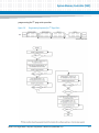
1
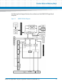
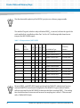
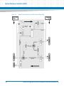
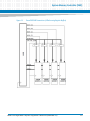
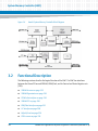
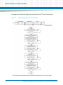
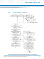
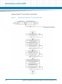
System Memory Controller (SMC) 3.2.2 SDRAM Organization The SDRAM is organized as 1, 2, 3, 4, 5, 6, 7, or 8 blocks, 72 bits wide with 64 of the bits being normal data and the other 8 being checkbits. The 72 bits of SDRAM for each block can be made up of x4, x8, or x16 components or of 72-bit DIMMs that are made up of x4 or x8 components. The 72-bit, unbuffered DIMMs can be used as long as AC timing is met and they use the components listed. All components must be organized with 4 internal banks. 3.2.3 PPC60x Bus Interface The SMC has a PowerPC slave interface only. It has no PowerPC master interface. The slave interface is the mechanism for all accesses to SDRAM, ROM/Flash, and the internal and external register sets. This section discusses the following topics: 3.2.3.1 Responding to Address Transfers on page 196 Completing Data Transfers on page 197 PPC60x Data Parity on page 197 PPC60x Address Parity on page 197 Cache Coherency on page 198 Cache Coherency Restrictions on page 198 L2 Cache Support on page 198 Responding to Address Transfers When the SMC detects an address transfer that it is to respond to, it asserts AACK_ immediately if there is no uncompleted PPC60x bus data transfer in process. If there is one in process, then the SMC waits and asserts AACK_ coincident with the uncompleted data transfer’s last data beat if the SMC is the slave for the previous data. If it is not, it holds off AACK_ until the CLK after the previous data transfer’s last data beat. 196 MVME5100 Single Board Computer Programmer’s Reference (6806800H17B)