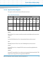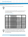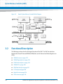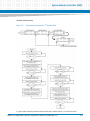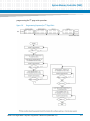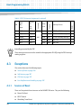
1
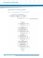
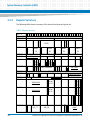
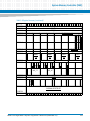
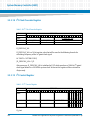
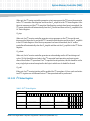
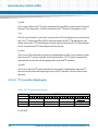
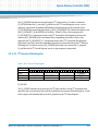
System Memory Controller (SMC) Some registers have additional requirements for writing. For more information refer to the registers in SDRAM Enable and Size Register (Blocks A, B, C, D) on page 234, SDRAM Base Address Register (Blocks A/B/C/D) on page 236, SDRAM Enable and Size Register (Blocks E,F,G,H) on page 260, SDRAM Base Address Register (Blocks E/F/G/H) on page 261, and SDRAM Speed Attributes Register on page 262. Since software has no way of controlling refresh/scrub accesses to SDRAM, the hardware is designed so that updating control bits coincidentally with refreshes is not a problem. As with SDRAM control bits, software should not change control bits that affect ROM/Flash while the affected Block is being accessed. This generally means that the ROM/Flash size, base address, enable, write enable, etc. are changed only while executing initially in the reset vector area ($FFF00000 - $FFFFFFFF). 3.4.3 Initializing SDRAM Related Control Registers In order to establish proper SDRAM operation, software must configure control register bits in Hawk that affect each SDRAM block’s speed, size, base address, and enable. The SDRAM speed attributes are the same for all blocks and are controlled by one 32-bit register. The size, base address and enable can be different for each block and are controlled in individual 8- bit registers. The following topics are discussed in this section: 270 SDRAM Speed Attributes on page 271 SDRAM Size on page 271 I2C EEPROMs on page 271 SDRAM Base Address and Enable on page 271 SDRAM Control Registers Initialization Example on page 271 Optional Method for Sizing SDRAM on page 277 MVME5100 Single Board Computer Programmer’s Reference (6806800H17B)