1
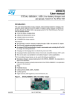
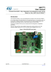
UM1471
User manual
250 W DC-DC solar module for photovoltaic distributed architecture
Introduction
The STEVAL-ISV013V1 is a fully integrated module designed for a smart junction box in
distributed photovoltaic architecture. The module represents an easy-to-use, fully-protected
solution to implement precise photovoltaic panel control, diagnostic and protection.
The STEVAL-ISV013V1 is the base element for a new photovoltaic panel configuration able
to increase the panel energy produced and to simplify the photovoltaic field design and
realization. Furthermore, the maintenance cost is reduced thanks to the possibility of
monitoring the individual panel status and to communicate these data to a remote control
unit. The demonstration board realizes an isolated converter to be connected at the output
of a single PV panel for distributed MPPT. This voltage is stepped up to the voltage, defined
by the inverter, needed to realize a sinusoidal output with a magnitude big enough to
transfer energy in the grid.
The module features an embedded MPPT (maximum power point tracking) algorithm based
on the “Perturb and Observe” (P and O) technique to search for the best operating point of
the panel in order to maximize the energy produced in every environmental condition.
The module is internally protected against surge or lightning reaching the connection wires.
The STEVAL-ISV013V1 can integrate a PLM or ZigBee® for communication. The PLM is
supported by a proprietary protocol stack for networking. Gateway to RS485 in Modbus is
available. The unit is designed to operate in a harsh environment offering a high level of
protection and very high reliability.
The ZigBee® module is based on system-on-chip (SoC) technology, integrating both IEEE
802.15.4 radio transceiver and computing capabilities and is designed to run a fully
compliant ZigBee® PRO network protocol stack.
Figure 1.
July 2012
STEVAL-ISV013V1 image
Doc ID 022251 Rev 1
1/15
www.st.com
Contents
UM1471
Contents
1
System description . . . . . . . . . . . . . . . . . . . . . . . . . . . . . . . . . . . . . . . . . . 4
2
Application circuit . . . . . . . . . . . . . . . . . . . . . . . . . . . . . . . . . . . . . . . . . . . 7
3
Electrical schematics . . . . . . . . . . . . . . . . . . . . . . . . . . . . . . . . . . . . . . . . 8
4
Digital control description . . . . . . . . . . . . . . . . . . . . . . . . . . . . . . . . . . . 12
5
Overcurrent and overvoltage protections . . . . . . . . . . . . . . . . . . . . . . . 13
6
Revision history . . . . . . . . . . . . . . . . . . . . . . . . . . . . . . . . . . . . . . . . . . . 14
2/15
Doc ID 022251 Rev 1
UM1471
List of figures
List of figures
Figure 1.
Figure 2.
Figure 3.
Figure 4.
Figure 5.
Figure 6.
Figure 7.
Figure 8.
STEVAL-ISV013V1 image . . . . . . . . . . . . . . . . . . . . . . . . . . . . . . . . . . . . . . . . . . . . . . . . . . 1
STEVAL-ISV013V1 image with highlighted hardware sections . . . . . . . . . . . . . . . . . . . . . . 4
STEVAL-ISV013V1 - I/O connectors . . . . . . . . . . . . . . . . . . . . . . . . . . . . . . . . . . . . . . . . . . 6
Typical application system . . . . . . . . . . . . . . . . . . . . . . . . . . . . . . . . . . . . . . . . . . . . . . . . . . 7
Electrical schematic - power board and aux. power supply . . . . . . . . . . . . . . . . . . . . . . . . . 9
Electrical schematic - sensing circuit and gate driver section. . . . . . . . . . . . . . . . . . . . . . . 10
Electrical schematic - microcontroller and level translator . . . . . . . . . . . . . . . . . . . . . . . . . 11
MPPT algorithm embedded on 32-bit microcontroller STM32 . . . . . . . . . . . . . . . . . . . . . . 12
Doc ID 022251 Rev 1
3/15
System description
1
UM1471
System description
The STEVAL-ISV013V1 is a smart junction box for photovoltaic panels. It is a high efficiency
isolated DC-DC boost converter operating in the input voltage range from 10 V to 45 V and
able to step up the panel voltage to the input voltage of a DC-AC converter. In addition, it
provides metering and monitoring features and implements some safety functions like fire
and anti-theft protections.
A general description of the system is shown in Figure 2, with an image highlighting the
different hardware sections of the board.
Figure 2.
STEVAL-ISV013V1 image with highlighted hardware sections
/UTPUT"US6OLTAGE POSITIVE
RANGE66
06PANEL POSITIVE
6IN6
06PANEL NEGATIVE
6OUT 6
Ͳ
!UXILI ARY03SECTION
/UTPUT"US6OLTAGE NEGATIVE
!-V
It consists of several sections as listed below:
●
DC-DC converter
●
Auxiliary power supply
●
Digital control section
●
I/O connectors
●
PLM - ZigBee external module connector.
DC-DC converter section
The power section, based on an isolated full bridge boost converter, is designed to accept
low input voltage in the range 10-45 V. The output voltage is in the range 350-430 V, suitable
to directly supply the DC bus of a standard single-phase inverter.
The specifications in Table 1 for the PV system are used as inputs for the design of the DCDC converter.
4/15
Doc ID 022251 Rev 1
UM1471
System description
Table 1.
Main DC-DC converter specifications
Symbol
Parameter
Value
Unit
Operating condition
Vin
Input DC supply voltage range
10 to 55
V
Vin_MPPT
MPPT input DC voltage range
24 to 45
V
350 to 430
V
Vout
Operating output DC voltage
Iout
Operating output current
0.8
A
Fs
Switching frequency
35
kHz
Efficiency
Peak eff.
Peak efficiency
97.5%
-
Euro eff.
European efficiency
96.6%
-
MPPT-eff.
MPPT efficiency
99%
-
Auxiliary power supply section
The auxiliary power supply has been developed to provide stable supply voltage for different
electronic components, for example, gate-drivers, microcontroller, and operational
amplifiers.
In particular, the output voltages are the following:
●
+15 V to supply MOSFET gate-driver, PLM module
●
+5 V to supply level translator for gate driving
●
+3.3 V to supply microcontroller, operational amplifiers, level translator, ZigBee module.
This auxiliary power supply is developed to supply the module also from the output,
implementing anti-theft during the night. Under this condition, the PLM unit and ZigBee unit
are ON also under no solar irradiance condition. This feature is guaranteed by means of a
supply voltage on the DC bus provided by an external power supply.
Digital control section
The digital control section is managed by STM32, a microcontroller central unit based on
ARM Cortex™-M3 32-bit RISC core operating at a 72 MHz clock frequency.
●
The key features are:
–
1.25 DMIPS/MHz (Dhrystone 2.1) performance at 0 wait state memory access
–
Single-cycle multiplication and hardware division
–
128 Kbytes of Flash memory, 20 Kbytes of SRAM
–
12-bit, 1 µs A/D converter
–
DMA controller
–
16-bit timers with IC/OC/PWM
–
SysTick timer 24-bit downcounter
–
USART communication interface.
Doc ID 022251 Rev 1
5/15
System description
UM1471
The STM32Fx controls the operation of the DC-DC converter with MPPT algorithm,
monitors the input/output section with OVP and OCP, manages the synchronization with a
cascaded inverter and the interface with external communication module (PLM-ZigBee).
I/O connectors
The STEVAL-ISV013V1 module is developed to be connected with photovoltaic panels
(input side) and with inverters (output side). The areas 1 and 4, in Figure 3, are used to
connect the demonstration board with a standard solar panel (with proper junction box). The
areas 1-2-3-4 are used with a solar panel connected directly to this board. In this
configuration, area 5 is for bypass diodes or SPV1001 cool bypass switch, an integrated
smart diode by STMicroelectronics.
Figure 3.
STEVAL-ISV013V1 - I/O connectors
3OLARPANEL
BUSBAROR*"CABLES
/UTPUTCONNECTORS
FORSOLARCABLES
0,-:IG"EE
MODULECONNECTOR
!-V
PLM - ZigBee external module connector
The STEVAL-ISV013V1 is ready to be connected to a PLM or ZigBee external module for
communication. Figure 3 shows the communication board module connector. The power
supply for this module is provided by the main board.
6/15
Doc ID 022251 Rev 1
UM1471
2
Application circuit
Application circuit
Figure 4 shows the typical photovoltaic system architecture which can be realized with the
STEVAL-ISV013V1. It is worth noting that the distributed architecture is based on parallel
connection of smart panels in a high voltage DC bus. Thanks to this approach, the DC-DC
stage of the standard string inverter can be removed, reducing overall system complexity
and cost.
Figure 4.
Typical application system
Doc ID 022251 Rev 1
7/15
Electrical schematics
3
UM1471
Electrical schematics
The power board schematic is shown in Figure 5. The input voltage, given by the PV panel
in the range between 10 V and 55 V, is fed into the power circuit through the connector J1.
The need for boosting the low input voltage to the much higher DC link voltage, required for
interfacing with the inverter, is guaranteed by an isolated full bridge boost converter. The
input boost inductor (L1), placed at the input side, permits low ripple current values, the
output rectifying diodes (D1, D3) are placed across output capacitors, ensuring minimum
voltage stress and effective voltage clamping. A high frequency transformer (TR1) is used to
step up the input voltage and for functional isolation.
The auxiliary power supply, based on an isolated Flyback converter, provides the supply
voltage for the microcontroller, operational amplifiers, gate-drivers and level translator. The
flyback transformer (TR2) has two secondary regulated outputs for +5 V and +15 V.
An integrated voltage regulator (IC4) supplies the 3.3 V from 5 V. Figure 6 shows the section
for I/O sensing, in particular the panel output voltage and current are measured for
maximum power point tracking algorithm.
The output bus voltage is controlled for overvoltage protection (OVP) and to establish the
communication with the cascaded inverter.
8/15
Doc ID 022251 Rev 1
Doc ID 022251 Rev 1
-
'
"
&
*1'
.
5
&
10
/
/
10
["
'
76
&
"
5
.
5
.
&
S
5
.
5
.
9
&
"
&
Q
&
S
*1'
,&$
76
&
Q
5
.
&
"
9)%
&
Q
8& %
57&7
,6(16(
5
.
4
%&
*1'
287
9,
95()
5
.
+3$.
4
67+1)
5
.
5
RKP
"
5
.
5
RKP '
%$7
62'
'
%$7
4
%&
1060$
&
'
&
"
5
.
5
.
'
5
0
5
10
5
.
.
5
,&
76
5
.
5
0
5
.
5
0
+3$.
&
&
Q
'3$.
5
.
5
.
4
67'1)
677+5$
'
'
60$-
62'
'
1
9
4
%&
6285&(
"
75
4
67+1)
+3$.
4
67+1)
9287
5
0
9ROWDJHPD[9
5
0
76
5
RKP
&
4
00%7$
"
&
5
0
9,1387
',$0H
&
X
9
"
6285&(
*1'
&
Q
,&
76
5
.
&
Q
2XW
*$7(
'
60%-&$
4
67+1) 60%
*$7(
+3$.
9ROWDJHPD[9
,&$
76
0
5
&
"
,B6(16B39
'
1
5
.
&203
,&
5
.
.
5
.
5
.
2XW
*$7(
0
5
5
0
4
&
S
9
&
/
X+ $
*$7(
X9
00%7$
5
9
&
10
&
*1'
X
5
.
Q
&
10
60$60%
'
60$
[
&
Q
671+1 .
10
'
5
0
4
5
0
P2KP
5
60%
'
10
9ROWDJHPD[9
5
.
9,1387
,B6(16B39
5
.
9,1B6(16B39
P+
',$0H
*1'
*1'
5
.
&
Q
&
X
9
5
.
5
RKP
5
10
5
10 60%
'
677+/8
639'
9,1387
639'
'
'
639'
-63$5(
-63$5(
)SOLATEDFULLBRIDGE
BOOSTCONVERTER
-
RKP
5
5
RKP
'3$.
75
&
75
'
Q9
&
[
/
X+
60$
&
X 9
5
RKP
9
&
X
VRW
,1387 287387
*1'
&
5
10
-3
*1'
62'
'
9
&
X 9
-3
9
'
10
5
.
9287B(;7
X9
[
S
9EXVB6(16
[
X+
/
5
.
5
0
5
0
10
/
,&
/'$%875
5
.
5
RKP
9
&
S
6736+ 60%60$
6736/
'
X9
&
X9
5
RKP
9
&
S
'
677+5*
9ROWDJHPD[9WR*1'
'3$.
'
677+5*
*1'
*1'
9
9
9&&
9287
-
&21
9
&
X
Figure 5.
RKP 5
)86(
)
9287
UM1471
Electrical schematics
Electrical schematic - power board and aux. power supply
!UXILIARYPOWERSUPPLY
!-V
9/15
9&&
Doc ID 022251 Rev 1
5
10
&
10
$'&B3$1(/B92/7$*(
3:0B9
3:0B9
.
5
&
Q
.
6285&(
/9*
287
+9*
9ERRW
677+$
/(
*1'
9FF
+,1
/,1
,&
'
/9*
287
+9*
9ERRW
6285&(
/(
*1'
9FF
+,1
/,1
677+$
60$
&
X)
&
X)
'
'
'
'
'
'
'
'
,Q
,Q
287
9FF
9
769%,'
9FF
,Q
,Q
287
,&
.
5
5
10
&
Q
Q
&
10
&
5
.
5
.
5
5
9,1B6(16B39
.
&
10
RKP
5
RKP
RKP
5
RKP
5
5
RKP
RKP
5
5
RKP
RKP
5
$IODES3403!
2ESISTORSSIZE
066/,4!'% 3%.3).'3%#4)/.
&
Q
.
5
.
5
5
,&
'
*DWH
2XW
*DWH
*DWH
2XW
*DWH
,B6(16B39
,B6(16B39
5
6
6
-3
9
5
.
6(/
'
5
10
10
5
769%,'
9FF
,Q
,Q
287
5
.
5(6(7
7567
7',
7'26:2
7&.6:&/.
&
10
5
.
5 .
&
10
5 .
7066:', 2
& Q)
3%
6,*1$/B,39
&
Q
&
10
,&
.
5
,Q
,Q
287
9FF 9
6"533%.3).'
.
5
10
&
10
&
Q
&
Q)
&
,&
,1
9
5
.
&
.
5
5
.
5
.
Q)
&
5
.
5
10
9
$'&B3$1(/B&8 55(17
$'& B%86B92/7$*(
287
9
10
76,'7
,1
&21
-
5
.
5
.
06#522%.43%.3).'3%#4)/.
.
,&
67*'75
9
9EXVB6(16
.
5
9&&
*1'
9
10/15
9
Figure 6.
$#$#$RIVERSECTION
Electrical schematics
UM1471
Electrical schematic - sensing circuit and gate driver section
!-V
*1'
/
Doc ID 022251 Rev 1
)5(4
6:
2KP
5
*1'
&
Q
'2:1
5
2KP
3%7,0B&+
5
2KP
3% 5
.
3:0
3$
*1'
S
&
3% 6:
2KP
5
9
*1'
&
Q
83
5
.
6:
2KP
5
9
*1'
9
*1'
&
Q
5
.
*1'
.
5
.
5
3% 3%
$549#9#,%"544/.3/.,9&/2$%"5'
3$
3$ 3$
5
2KP
3$ S
3$ S
3$ &
3% &
*1'
3$ 3$ 3$
3% *1'
*1'
&
X9
3% 9
3$
3$
966B $'&B3$1(/B&855(17
$'&B3$1(/B92/7$*(
$'&B%86B92/7$*(
&
Q
Q
&
3%
3%
3%
3%
3$
3$
3$
3$
3$
3$
966B
9''B
9'' B %/03*61/
'2:1
3$:.83
9''$
966$
1567
3'26&B287
3'26&B,1
3&26&B287
3&26&B,1
3$ 3$7,0B&+
9'' B
-803(5)250337(1$%/(
%227
-3
)5(4
*1'
9
3%
3:0
3:0
9
&21$
-
*1'
&
S
*1'
*1'
67
1567
N
5
1&
1&
,29/
, 29&&
,29/
, 29&&
*1'
5
N
,& 9&& 9/
*1'
&
Q
5
N
9 9
-352/81*$ #/..%44/2)342)0,).%
3$7,0B&+
3%7,0B&+
5(6(7
.
5
5(6(7&,5&8,7
7066:',2
*1'
$%"5'#/.. %#4/2 -3
9
3%
3%
3%
3%
3$
3$
3$
3$
3$
3$-7$*
3:0
3:0
$'&B3$1(/B&85 5(17
$'&B3$1(/B92/7$*(
$'&B%86B92/7$*(
6,*1$/B,39
3%
3$
3$
9
*1'
&
Q
9
2(
9
3:0
966 B
*1'
3% 670)&%7
,1&0
3% %2 27 83
1567
3% 2KP
S
3% &
3% 5
3% 6,*1 $/B,39
<
0K]
3% 75 67
3&7$03(5B57&
7' 26: 2
3% 3$ 9%$7
S
&
3$ - 7 $*
*1'
*1'
2KP
5
,&
*1'
3$ - 7 $*
*1 '
&2%15%.#9"544/.3/.,9&/2$%"5'
&
S
<
.K]
Q
&
3% 3%
) 5 (4
5
2KP
9
7',
.
5
7& .6: & /.
&
S
9
*1'
9
&
Q
3&%$
*1'
&
Q
5(6(7
675,33,1
6:
3:0B9
3:0B9
-
&21
*1'
&
S
9&&
*1'
3$
3$
9
9
*1'
*1'
&
S
3$
3$
23
576B
&76B
7;'B
5;'B
*1'
&
S
0,-:)'"% %#/..%#4 /2
0#O R0# *1'
&
S
3%
3%
3%
3%
3%
3%
3%
3%
3$
9287B(;7
9287
*1'
&
S
9
Figure 7.
*1'
%227
-3
UM1471
Electrical schematics
Electrical schematic - microcontroller and level translator
!-V
11/15
Digital control description
4
UM1471
Digital control description
The overall control architecture requires three feedback signals for correct operation, input
panel current and input panel voltage are used for maximum power point tracking; the output
bus voltage is used for monitoring OV condition and to control the starting/stopping
procedure.
These signals are sent to the ADC inputs of the microcontroller, according to the pin
assignment of Figure 7, and in function of these values, two timers generate PWM output to
drive the full bridge power MOSFETs or disable the driving signals to turn off the module,
isolating the solar panel from the output bus. The duty cycle value is regulated by a
maximum power point tracking algorithm implemented by the STM32 microcontroller
(Figure 8).
Figure 8.
MPPT algorithm embedded on 32-bit microcontroller STM32
$#$#
#ONVERTER
(
$#
/UTPUT
2ESISTORDIVIDER FOR!$# SENSING
$#$UTYCYCLEVALUE
#$UTYCYCLESTEPVALUE
6K)NPUT VOLTAGE
0K0OWER
6
0
6
$#
6SENSE
(
(
3ENSE6K)K
)SENS
0K6K
)K
34- -ICROCONTROLLER
!$
CONVERTER
.EW$UTYCYCLE
VA LUECALCULATED
0REVIOUS
0OWERAND)NPUT
6OLTAGEVA LUE
REGISTER
-004
#ONTROLLER
.O
6K6+ 6K6+ .O
$#$# #
9ES
0K0K 9ES
$#$##
.O
$#$# #
9ES
$#$##
!-V
12/15
Doc ID 022251 Rev 1
UM1471
5
Overcurrent and overvoltage protections
Overcurrent and overvoltage protections
The overcurrent and overvoltage protections have been implemented in order to avoid
damaging the hardware. The short-circuit and the open circuit condition at the output
connectors (Vout+, Vout-) of the junction box forces the microcontroller to isolate the solar
panel from the output. At the changed condition, the system restarts following the start-up
procedure. The output voltage is limited via firmware at 430 V.
Doc ID 022251 Rev 1
13/15
Revision history
6
UM1471
Revision history
Table 2.
14/15
Document revision history
Date
Revision
27-Jul-2012
1
Changes
Initial release.
Doc ID 022251 Rev 1
UM1471
Please Read Carefully:
Information in this document is provided solely in connection with ST products. STMicroelectronics NV and its subsidiaries (“ST”) reserve the
right to make changes, corrections, modifications or improvements, to this document, and the products and services described herein at any
time, without notice.
All ST products are sold pursuant to ST’s terms and conditions of sale.
Purchasers are solely responsible for the choice, selection and use of the ST products and services described herein, and ST assumes no
liability whatsoever relating to the choice, selection or use of the ST products and services described herein.
No license, express or implied, by estoppel or otherwise, to any intellectual property rights is granted under this document. If any part of this
document refers to any third party products or services it shall not be deemed a license grant by ST for the use of such third party products
or services, or any intellectual property contained therein or considered as a warranty covering the use in any manner whatsoever of such
third party products or services or any intellectual property contained therein.
UNLESS OTHERWISE SET FORTH IN ST’S TERMS AND CONDITIONS OF SALE ST DISCLAIMS ANY EXPRESS OR IMPLIED
WARRANTY WITH RESPECT TO THE USE AND/OR SALE OF ST PRODUCTS INCLUDING WITHOUT LIMITATION IMPLIED
WARRANTIES OF MERCHANTABILITY, FITNESS FOR A PARTICULAR PURPOSE (AND THEIR EQUIVALENTS UNDER THE LAWS
OF ANY JURISDICTION), OR INFRINGEMENT OF ANY PATENT, COPYRIGHT OR OTHER INTELLECTUAL PROPERTY RIGHT.
UNLESS EXPRESSLY APPROVED IN WRITING BY TWO AUTHORIZED ST REPRESENTATIVES, ST PRODUCTS ARE NOT
RECOMMENDED, AUTHORIZED OR WARRANTED FOR USE IN MILITARY, AIR CRAFT, SPACE, LIFE SAVING, OR LIFE SUSTAINING
APPLICATIONS, NOR IN PRODUCTS OR SYSTEMS WHERE FAILURE OR MALFUNCTION MAY RESULT IN PERSONAL INJURY,
DEATH, OR SEVERE PROPERTY OR ENVIRONMENTAL DAMAGE. ST PRODUCTS WHICH ARE NOT SPECIFIED AS "AUTOMOTIVE
GRADE" MAY ONLY BE USED IN AUTOMOTIVE APPLICATIONS AT USER’S OWN RISK.
Resale of ST products with provisions different from the statements and/or technical features set forth in this document shall immediately void
any warranty granted by ST for the ST product or service described herein and shall not create or extend in any manner whatsoever, any
liability of ST.
ST and the ST logo are trademarks or registered trademarks of ST in various countries.
Information in this document supersedes and replaces all information previously supplied.
The ST logo is a registered trademark of STMicroelectronics. All other names are the property of their respective owners.
© 2012 STMicroelectronics - All rights reserved
STMicroelectronics group of companies
Australia - Belgium - Brazil - Canada - China - Czech Republic - Finland - France - Germany - Hong Kong - India - Israel - Italy - Japan Malaysia - Malta - Morocco - Philippines - Singapore - Spain - Sweden - Switzerland - United Kingdom - United States of America
www.st.com
Doc ID 022251 Rev 1
15/15