1
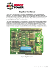
Evaluation Board for
MMnet01/101
User
Manual
REV 0.8
,
lu ard ST Sta rve
a
,
e
o
Ev B VR ers b S l
d
n
io 1, A trol We mo
t
a ‘5
n d
ni ri
o
e
r
c
fo cro dd s M the
e
s
d e
i
m mb oar rs, peC E B
e S
PI its ng roll gh r
K pi nt Hi fo
r
y
o
rte tot roc FID ers s
o c
r
Pr mi s, R mm lle
rs or ler gra tro
f ol
n
o
s
pr oco CB
e ntr
l
u o
m icr s, P for
c
e
t
t
m m ds
s
ne Sy T
te ar s
S
l
n
I
,
sy Bo tro
C
d
e PI or ion on b
,
es at roc We
R
c
u
AV pro val mic ed iro E
dd
ic ng PIC be ds m
M ni T, m
r
g S E oa rs,
i
s
, ts
e
B
de VR Ki ng roll
t
h
A ter pi
n
g
i
,
y
o
t
1 r
H
‘5 Sta oto roc ID c
r
e
rs P mi RF m
e
s
l
,
r
er fo ers ram trlv
g n
r
s
ll
Se ule tro pro oco
od con ms icr s,
m
ni net ste T m stem
er Sy , S sy Bo
h
et d In PIC sor on e
, ce ati
ic
e
R
m
o
u
Sp AV opr val IC e
r r
fo ic g E T, P mb
rs s M nin , S
E g
s
r
t
g
R
i
i
in
le
ol des , AV er K typ
B `51 tart roto roS s P mic ,
PC for
s
s ller
er for llers
d
ar tro erw les tro on b S du con ram
c
ro We imo et rog o
n
p
n
ed Mi her m roc
d
d ds et ste ic
ar rs, Sy T m r
o
B olle In , S so
tr ed IC oce ign
P
s
co Spe R, opr De
V cr
h
B Rtion
ig r A Mi
C
a
H f o rs
, Pone asolution
lu
Many ideas
s
e
s
l
v s
m
er ol
m ntr ste g E ard
co Sy nin Bo
Contents
1 INTRODUCTION ....................................................................................................................................... 3
FEATURES .................................................................................................................................................... 3
2
THE BOARD.......................................................................................................................................... 4
PLACEMENT OF ELEMENTS ON THE BOARD ................................................................................................. 4
ARRANGEMENT ON LEAD-OUTS ................................................................................................................... 5
BOARD SUPPLY ............................................................................................................................................ 5
LED DIODES ................................................................................................................................................. 6
PUSH-BUTTONS ............................................................................................................................................ 6
LCD DISPLAY ............................................................................................................................................... 7
POTENTIOMETERS........................................................................................................................................ 7
BUZZER ........................................................................................................................................................ 8
RESET BUTTON .......................................................................................................................................... 8
RS-232 INTERFACE ..................................................................................................................................... 9
USB INTERFACE ........................................................................................................................................ 10
1-W IRE INTERFACE .................................................................................................................................... 11
ISP AND JTAG CONNECTORS ................................................................................................................... 11
3
TECHNICAL ASSISTANCE ............................................................................................................. 13
4
GUARANTEE ...................................................................................................................................... 13
5
BOARD LAYOUT AND DIMENSIONS ........................................................................................... 14
6
SCHEMATICS ..................................................................................................................................... 14
1 Introduction
The EVBnet01 board was created with the aim of providing a hardware base for a designer of
systems relying on the MMnet01/101 minimodules, allowing to realize and verify quickly one’s
own ideas. Having this in mind, the board has been designed in such a way that the user has
access to all terminals of the module which are led out to connectors. The board houses also
such peripherals as: LEDs, push-buttons, potentiometers, a LCD display, a RS232 and USB
interface, a 1-Wire connector. All these elements are accessible through pin connectors,
permitting their connection with any processor port. The board has also a large prototype area
which permits the designer to connect other elements in any configuration. Due to the incision (vcut) between the prototype area and the rest of the board, the prototype part can be broken off.
The board contains also a power supply which relieves the user from the need to provide a
regulated supply voltage.
Together with the board, we deliver source codes of the Nut/OS together with the TCP/IP stack as
well as demonstration software.
The EVBnet01 along with the MMnet01/101 minimodule can be also used in didactic laboratories
of informatics colleges and universities, illustrating aspects of co-operation of electronic circuits
with the Ethernet/Internet networks. It can be also used to build circuits realizing thesis projects.
Features
•
•
•
•
•
•
•
•
•
•
•
•
•
•
•
•
•
Socket for the MMnet01/101 module
Connector with all terminals of the MMnet01/101 module
Connectors of all peripherals accessible on board
+5V power supply
Power switch
USB port (with use of MMusb232 minimodule)
RS232 port
1-Wire connector
Connector for In System Programming
Multiplexer separating the ISP connector from the rest of the system
JTAG connector for in system programming and debugging
(1)
connector for 2x16 LCD display
8 LED diodes
4 push-buttons
2 potentiometers
Buzzer
Prototype design area
Notice: 1. Mounted optionally
3
2 The Board
Placement of elements on the board
Figure 1 Placement of elements on the EVBnet01 board.
1.
2.
3.
4.
5.
6.
7.
8.
9.
10.
11.
12.
13.
14.
15.
16.
17.
Prototype area
Connector with led-out MMnet01/101 module terminals
MMnet01/101 minimodule
MMusb232 minimodule
RS232 connector
Supply connector
Power switch
Programming connector in the JTAG system
Programming/emulation connector in the JTAG system
LCD display
LED diodes
Push-buttons
Potentiometers
RESET button
1-Wire connector
Peripheral connectors
Buzzer
4
Arrangement on lead-outs
Function in MMnet01/101
Interrupt from RTL8019AS
DataFlash - MOSI
Bank select (optional)
Name
Name
Function in MMnet01/101
PE7
1
2
PE6
PE5
3
4
PE4
PE3
5
6
PE2
PE1
7
8
PE0
AREF
9
10
ADC0
ADC1
11
12
ADC2
ADC3
13
14
ADC4
ADC5
15
16
ADC6
ADC7
17
18
TOSC1
TOSC2
19
20
#RESET
PB0
21
22
PB1
DataFlash – SCK
PB2
23
24
PB3
DataFlash – MISO
PB4
25
26
PB5
DataFlash – #CS
PB6
27
28
PB7
PD0
29
30
PD1
PD2
31
32
PD3
PD4
33
34
PD5
PD6
35
36
PD7
LACT
37
38
LLNK
+5V
39
40
GND
Board supply
The EVBnet01 board can be supplied in two ways:
•
•
From an external power supply with an output of 7-12 V AC or 9-15 V DC, having a standard plug with
a bolt diameter of 2.1 mm, connected to supply socket J3. In case of a DC supply voltage its polarity
is irrelevant. Power is supplied to the module through JP11 jumper, which allows measurment of
module current consupltion. During normal operation this jumper should be cosed.
From USB connector. In this case JP1 jumper should be closed. Board houses also USB power
switch, which allows drawing up to 500mA from USB bus.
Notice: Both supply methods should not be used simultaneously.
5
The regulated + 5 V voltage is led out to the J1 connector (+ 5V) and J14 (GND).
D2
1
2
3
POWER
2
J3
4
BR1
RB152
+
-
1N4148
SW1
1
3
+
C8
470u/25V
Vin
Vout
GND
U4
7805
C13
100n
+5V
C12
100n
+
C11
47u/16V
D11
PWR
R22
1k
GND
Figure 2 Implementation of the power supply on the EVBnet01 board.
LED diodes
The EVBnet01 has 8 LED diodes which play the role of the simplest interface between the system and the
user. The board is constructed in such a way that it allows any connection between the diodes and
microcontroller leads. A diode lights up when a low signal level is applied to appropriate leads. The LED
current flowing into the microcontroller pin is about 3 mA.
+5V
1
3
5
7
LEDn
J10
2
4
6
8
D10
LED0
R15 1k
D9
LED1
R14 1k
D8
LED2
R13 1k
D7
LED3
R12 1k
D6
LED4
R11 1k
D5
LED5
R10 1k
D4
LED6
R9 1k
D3
LED7
R8 1k
Figure 3 Implementation of LED diodes.
Push-buttons
The EVBnet01 board is equipped with four microswitches which can be connected to any lead of the
microcontroller. Pushing a button causes a low state on any port terminal.
6
+5V
R19 R18 R17 R16
10k 10k 10k 10k
1
3
SWn
SW0
2
4
SW1
J12
SW2
SW3
GND
Figure 4 Implementation of push-buttons.
LCD display
EVBnet01 has place for standard 2x16 characters LCD display with HD44780 compatible controller. Display
terminals D4-D7, RS, E, contrast and backlight are led to LCD connector J7. LCD connector is designed in
this way, that it is possible to connect contrast signal to onboard potentiometer with use of jumpers, or with
use of wire to any microcontroller pin, that can generate PWM (through RC low pass filter, which can be built
on prototype area). Similarly, LCD backlight can be permanently turned on by closing jumper, or can be
controlled by any microcontroller pin.
Because LCD connector contains only higher part of display bus, it has to work 4-bit mode. Also, RW line is
permanently connected to ground, what allows only read operation, but it is sufficient to proper operation.
Such approach minimizes required microcontroller port pins to six.
+5V
R4
7k5
R5
1k
GND
CONTRAST
C15
100n
+5V
1
3
5
7
9
2
4
6
8
10
J7
LGT
GND
Figure 5 Default LCD configuration
– backlight permanently turned on,
contrast regulated with R5
potentiometer.
GND
+5V
Vc
LCD_RS
LCD_RW
LCD_E
D0
D1
D2
D3
D4
D5
D6
D7
A
K
GND
+5V
+5V
R24
1k
Q2
BC 817
J11
1
2
3
4
5
6
7
8
9
10
11
12
13
14
15
16
LCD 2x16
GND
Figure 6 Connection of LCD display on the board.
Potentiometers
7
EVBnet01 has two potentiometers, POT0 and POT1. The potentiometers can be used to simulate the outputs
of analog circuits. The voltage across POTx terminals can be adjusted in the 0....REF range.
1
3
2
4
3
AREF
3
J13
2
2
1
1
R20
10k
POT1
R21
10k
POT0
GND
Figure 7 Implementation of potentiometers.
Buzzer
The board has a built-in acoustic signaler, controlled by a logic low state through a transistor. The base of the
transistor is connected to connector J13 as SPK.
1
3
2
4
J13
+5V
R6
Q1
BC 857
10k
LS1
C17
CAP
GND
GND
BUZZER
Figure 8 Implementation of the Buzzer.
RESET button
The EVBnet01 board has a led-out RESET signal which can be used as the output to reset external circuits
and as the input to reset the module, e.g. through the RESET push-button. The EVBnet01 board is equipped
with an on-board resetting button; by pressing it we force a low state on the RESET terminal of the module.
8
+5V
R7
4k7
#RESET
SW6
RESET
GND
C16
100n
GND
Figure 9 Implementation of the RESET button.
RS-232 interface
The EVBnet01 board has one port for serial
RS232 transmission with a DB-9 connector. The
lead-outs TxD, RxD, RTS, CTS are applied to
the jumpers through a MAX232 level converter.
The DSR and DTR signals have been shorted.
Applying jumpers causes the connection of TxD
and RxD to the USART0 port of the
microcontroller and of CTS and RTS signals to
line PE2 and PE3, respectively. Signals of the
RS232 port can be connected also to any leadouts of the microcontroller by means of cables.
Notice: if flow control has not been implemented,
signals CTS and RTS should be connected to
each other by means of a jumpers (as shown in
the figure) in order to assure proper
communication.
9
+5V
+5V
+
2
6
J4
GND
V-
C1C2+
C2-
GND
14
7
13
8
T1 OUT
T2 OUT
R1 IN
R2 IN
MAX232
GND
3
4
C4
100n
D12
TX
R26
1k
D13
RX
R27
1k
+ C5
100n
GND
5
9
4
8
3
7
2
6
1
1
+
C7
100n
+
C1+
+5V
T1 IN
T2 IN
R1 OUT
R2 OUT
PE1 (TXD0)
JP3
5
11
10
12
9
PE2
RS232_TXD
RS232_RTS
RS232_RXD
RS232_CTS
JP4
PE0 (RXD0)
JP2
PE3
JP5
15
GND
V+
+5V
16
U1
VCC
C6
100n
GND
DB9F
Figure 10 Connection of the RS-232 port to the MMnet01/101.
USB interface
The EVBnet01 board has also USB port, realized with use of MMusb232 minimodule.
2
GND
M2
MMusb232
C2
100nF
JP10
+5V
R25
1k
1
2
3
4
5
6
7
8
9
10
11
12
TXL
PCT
PEN
TXE
RI
DCD
DSR
DTR
CTS
RTS
RxD
TxD
VPO
VEX
VIO
RXL
SLP
GND
3V3
GND
RSO
RST
GND
NC
24
23
22
21
20
19
18
17
16
15
14
13
GND GND
1
7, 8
Q3A
IRF7104
USB_RXD
PD2 (RXD1)
JP6
USB_TXD
PD3 (TXD1)
JP1
USB_CTS
PD5
JP8
USB_RTS
JP9
PD4
Figure 11 Connection of the USB port to the MMnet01/101.
Additionally board is equipped with USB power switch (based on Q3), with allows, accordingly to USB
specification, drawing up to 500mA from USB bus. For proper operation of this switch it is required that „Pull
Down IO Pins in USB Suspend” option in FT232BM settings is enabled.
The terminals TxD, RxD, RTS, CTS are connected to the jumpers. The DSR and DTR signals have been
shorted
10
Applying jumpers causes the connection of TxD and RxD to
the USART1 port of the microcontroller and of CTS and RTS
signals to line PD5 and PD4, respectively. Signals of the
RS232 port can be connected also to any lead-outs of the
microcontroller by means of cables.
Attention: if flow control has not been implemented, signals
CTS and RTS should be connected to each other by means of
a jumpers (as shown in the figure) in order to assure proper
communication.
1-Wire Interface
The EVBnet01 board has a 1-Wire bus connector. This connector can be used to connect e.g. a digital
DS1820 thermometer or Dallas/Maxim iButton reader from. The data signal has been applied to the J13
connector and designated as 1-W. It can be connected to any microcontroller lead-out by means of the
attached cable.
V TG
DATA
GN D
+5V
1
1
3
2
4
J13
R2
2k2
+5V
J2
R1
100R
1
2
3
1-WIRE
GND
1WIRE
Figure 12 Connection of the 1-Wire connector.
ISP and JTAG connectors
Programming of the module can be effected through the ISP or JTAG interfaces (the second one permits also
debugging in the system).
The ISP standard programmer communicates with the microcontroller through a three-wire SPI interface (plus
the RESET signal and power supply). The interface uses the I/O pins of the microcontroller (PE0, PE1 and
PB1) which, after programming, can perform usual functions. The LED signal controls the operation of
multiplexer U3 which disconnects, for the duration of the programming session, the ISP bus lines from the
peripheral circuits of the board, thus eliminating the possibility of an accidental writing operation into these
circuits. During the writing operation this line should be in the low state. The JP7 short allows manual control
of the multiplexer in case of using a programmer which is not serving this line.
11
JTAG is a four-lead interface permitting the takeover of control over the processor’s core and its internal
peripherals. The possibilities offered by this interface are, among others: step operation, full-speed operation,
equipment and program pitfalls, inspection and modification of contents of registers and data memories. Apart
from this, functions are available offered by ISP programmers: programming and readout of Flash, EEPROM,
fuse and lock bits.
J8
TCK ADC4
TDO ADC6
TMS ADC5
+5V
TDI ADC7
1
3
5
7
9
2
4
6
8
10
GND
+5V
#RESET
GND
JTAG
PE1
J6
GND
GND
GND
GND
+5V
10
8
6
4
2
9
7
5
3
1
PB1
#RESET
PE0
GND
ISP
+5V
R3
1k
D1
ISP
12
13
U3
X0
X1
2
1
Y0
Y1
5
3
X
Y
Z
14
15
4
PE1_M
PB1_M
PE0_M
Z0
Z1
6
11
10
9
INH
A
B
C
VDD
VSS
VEE
16
8
7
+5V
GND
GND
4053
JP7
ISP Enable
GND
Figure 13 Connection of the MMnet01/101 module with the JTAG connector.
1
MOSI
LED
RST
SCK
MISO
2
9 10
VCC
GND
GND
GND
GND
Figure 14 ISP connector.
TCK
TDO
TMS
VCC
TDI
1
2
9 10
GND
Vref
NSRST
NTRST
GND
Figure 15 JTAG connector.
Pin description
MOSI
Commands and data from programmer to target
LED
Multiplexer and LED diode driving signal
RST
RESET signal
SCK
Serial Clock, Controlled by programmer
MISO
Data from target AVR to programmer
VCC
Supply voltage to the programmer
GND
Ground
TCK
TDO
TMS
VCC
TDI
Vref
RST
GND
Pin description
Test Clock, clock signal from emulator to target
Test Data Output, data signal from target to emul.
Test Mode Select, mode select signal from
emulator to target
Supply voltage to the emulator
Test Data Input, data signal from emul. to target
Target voltage sense
RESET signal
Ground
Programmers which may be used with EVBnet01 and MMnet01/101 may be found on pages:
- ISPCable I: http://www.propox.com/products/t_77.html?lang=en
- ISPCable II: http://www.propox.com/products/t_78.html?lang=en
12
JTAG programmer/emulator may be found on page:
- JTAGCable I: http://www.propox.com/products/t_99.html?lang=en
3 Technical assistance
In order to obtain technical assistance please contact [email protected] . In the request please
include the following information:
•
•
•
Number of the board version (e.g. REV 2)
Setting of resistors
A detailed description of the problem
4 Guarantee
The EVBnet01 board is covered by a six-month guarantee. All faults and defects not caused by the user will
be removed at the Producer’s cost. Transportation costs are borne by the buyer.
The Producer takes no responsibility for any damage and defects caused in the course of using the EVBnet01
board.
13
5 Board layout and dimensions
6 Schematics
14
TPINTPIN+
TPOUTTPOUT+
+5V
R4
7k5
R5
1k
GND
+5V
Vc
LCD_RS
LCD_RW
LCD_E
D0
D1
D2
D3
D4
D5
D6
D7
A
K
GND
+5V
GND
CONTRAST
C15
100n
+5V
1
3
5
7
9
2
4
6
8
10
J7
LGT
GND
+5V
R24
Q2
BC 817
1k
J11
1
2
3
4
5
6
7
8
9
10
11
12
13
14
15
16
+5V
JP11
LCD 2x16
GND
J1_1
J1_2
J1_3
J1_4
J1_5
J1_6
J1_7
J1_8
J1_9
J1_10
J1_11
J1_12
J1_13
J1_14
J1_15
J1_16
J1_17
J1_18
J1_19
J1_20
J4_1
J4_2
J4_3
J4_4
TPINTPIN+
TPOUTTPOUT+
M1
PB0
PB1_M
PB2
PB3
PB4
PB5
PB6
PB7
PD0
PD1
PD2
PD3
PD4
PD5
PD6
PD7
LED_ACTIV
LED_LINK
+5V
PB0/SS
PE7/INT7
PB1/SCK
PE6/INT6
PB2/MOSI
PE5/INT5
PB3/MISO
PE4/INT4
PB4/OC0/PWM0
PE3/ACPB5/OC1A/PWM1A
PE2/AC+
PB6/OC1B/PWM1B PE1/PDO/TxD0
PB7/OC2/PWM2
PE0/PDI/RxD0
PD0/INT0/SCL
AREF
PD1/INT1/SDA
PF0/ADC0
PD2/INT2/RxD1
PF1/ADC1
PD3/INT3/TxD1
PF2/ADC2
PD4/IC1
PF3/ADC3
PD5
PF4/ADC4
PD6/T1
PF5/ADC5
PD7/T2
PF6/ADC6
LED_ACTIV
PF7/ADC7
LED_LINK
TOSC1
+5V
TOSC2
GND
#RESET
J2_1
J2_2
J2_3
J2_4
J2_5
J2_6
J2_7
J2_8
J2_9
J2_10
J2_11
J2_12
J2_13
J2_14
J2_15
J2_16
J2_17
J2_18
J2_19
J2_20
1
3
5
7
PE7
PE6
PE5
PE4
PE3
PE2
PE1_M
PE0_M
AREF
ADC0
ADC1
ADC2
ADC3
ADC4
ADC5
ADC6
ADC7
TOSC1
TOSC2
#RESET
2
4
6
8
J10
D10
LED0
R15 1k
D9
LED1
R14 1k
D8
LED2
R13 1k
D7
LED3
R12 1k
D6
LED4
R11 1k
D5
LED5
R10 1k
D4
LED6
R9 1k
D3
LED7
R8 1k
+5V
R19 R18 R17 R16
10k 10k 10k 10k
MMnet01/101
GND
SW0
1
3
2
4
SW1
J12
SW2
SW3
GND
J9
J8
TCK ADC4
TDO ADC6
TMS ADC5
+5V
TDI ADC7
1
3
5
7
9
PE6
PE4
PE2
PE0
ADC0
ADC2
ADC4
ADC6
TOSC1
#RESET
PB1
PB3
PB5
PB7
PD1
PD3
PD5
PD7
LED_LINK
GND
+5V
1
3
2
4
6
8
10
PE1
PB1
#RESET
PE0
GND
ISP
R3
1k
D1
ISP
JP7
2
1
5
3
6
11
10
9
U3
X0
X1
Y0
Y1
X
Y
Z
14
15
4
2
GND
2
1
R20
10k
ADJ1
R21
10k
ADJ0
+5V
R6
R23
10k
GND
4053
16
8
7
LS1
C17
100n
GND
GND
BUZZER
+5V
PB1_M
PE0_M
R7
4k7
+5V
VDD
VSS
VEE
Q1
BC 857
10k
PE1_M
Z0
Z1
INH
A
B
C
1
2
3
1-WIRE
GND
12
13
J2
R1
100R
GND
9
7
5
3
1
+5V
2
4
3
AREF
GND
+5V
#RESET
J6
10
8
6
4
2
+5V
R2
2k2
J13
3
2
4
6
8
10
12
14
16
18
20
22
24
26
28
30
32
34
36
38
40
Header 20X2
JTAG
GND
GND
GND
GND
+5V
1
3
5
7
9
11
13
15
17
19
21
23
25
27
29
31
33
35
37
39
1
PE7
PE5
PE3
PE1
AREF
ADC1
ADC3
ADC5
ADC7
TOSC2
PB0
PB2
PB4
PB6
PD0
PD2
PD4
PD6
LED_ACTIV
+5V
+5V
GND
GND
#RESET
SW6
RESET
C14
100n
GND
GND
ISP Enable
C16
100n
GND
GND
http://www.propox.com
email: [email protected]
Title: EVBnet01
Size:
Date: 31-03-2005
15
Rev:
File:
Sheet 1 of 2
1.00
+5V
C1
100n
+5V
+5V
+
2
6
J4
16
V-
C1C2+
C7
100n
+
GND
C1+
C4
100n
3
4
14
7
13
8
T1 OUT
T2 OUT
R1 IN
R2 IN
MAX232
GND
T1 IN
T2 IN
R1 OUT
R2 OUT
11
10
12
9
MH4
MH5
GND
GND
GND
GND
MH3
MH6
D13
RX
R26
1k
R27
1k
PE1 (TXD0)
JP3
5
PE2
RS232_TXD
RS232_RTS
RS232_RXD
RS232_CTS
JP4
PE0 (RXD0)
JP2
PE3
JP5
1
Q3A
IRF7104
VPO
VEX
VIO
RXL
SLP
GND
3V3
GND
RSO
RST
GND
NC
24
23
22
21
20
19
18
17
16
15
14
13
2
GND
7, 8
JP10
C2
100nF
not mounted
+5V
J5
TPINTPIN+
TPOUTTPOUT+
R25
1k
M2
MMusb232
1
2
3
4
Header 4
1
2
3
4
5
6
7
8
9
10
11
12
TXL
PCT
PEN
TXE
RI
DCD
DSR
DTR
CTS
RTS
RxD
TxD
USB
D12
TX
MH2
GND
DB9F
GND GND
+5V
+ C5
100n
C2-
GND
1
+
GND
5
9
4
8
3
7
2
6
1
V+
+5V
15
GND
RS-232
U1
VCC
C6
100n
GND
MH1
USB_RXD
PD2 (RXD1)
JP6
USB_TXD
PD3 (TXD1)
JP1
USB_CTS
PD5
JP8
USB_RTS
PD4
JP9
POWER
D2
1
2
3
2
J3
4
BR1
RB152
+
-
1
C8
470u/25V
Vin
Vout
GND
U4
7805
C13
100n
1
2
J1
1N4148
+5V
+5V
SW1
+
3
POWER
J14
GND
GND
1
2
+5V
C12
100n
+
C11
47u/16V
D11
PWR
R22
1k
GND
http://www.propox.com
email: [email protected]
Title: EVBnet01
Size:
Date: 31-03-2005
16
Rev:
File:
Sheet 2 of 2
1.00