1
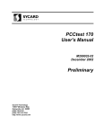
PCCextend 135 CardBus Extender User’s Manual Preliminary M200059-00 February 2003 Sycard Technology 1180-F Miraloma Way Sunnyvale, CA 94085 (408) 749-0130 (408) 749-1323 FAX http://www.sycard.com PCCextend 135 User’s Manual Page 1 1.0 Introduction Sycard Technology's PCCextend 135 CardBus extender card is designed for production and test environments where a external power supply is required for card test. An external power supply can provide accurate current measurements and voltage margin testing. • • • • • • • • Low profile design compatible with type I, II and III sockets 6-layer construction to insure a low noise environment Vcc, Vpp1, and Vpp2 can be supplied from an external source Screw terminals or 0.1” headers for quick external power connection Vcc LEDs indicate 3.3V or 5V operation SMT resistor pads allow user to isolate or add series resistors to any signal Convenient grounding posts for scope probes or other test equipment Low on-resistance MOSFET switches (less than 50 mOhm) 2.0 Setting up the PCCextend 135 The PCCextend 135 is a single piece extender card that can be inserted in Type I, II or III CardBus slots. Prior to inserting into the CardBus host the user should connect the external power supplies. Prior to connecting the external power supplies, the user should verify that the power supplies are set to Connections are made via the screw terminals at P3 or the 0.1” single row header at P4. Pin Power Connection 1 External VCC 2 External VCC 3 Ground 4 Ground 5 External VPP1 6 Ground 7 External VPP2 8 Ground Table 2.0.1 External Power Supply Connection Caution: Insertion and removal of the extender and PC card should be done with care. The PC Card's fragile connectors may be broken or bent if improper force is used. Both card and extender should be inserted straight without any lateral movement or force. Proper care and use of the extender card will insure years of trouble free operation. Note: Because of the configuration of the MOSFET switches it is only possible to supply a single voltage level to the Vpp1 and Vpp2 supplies. For example, if the external Vpp1 or Vpp2 power supplies are set to 12V and the host’s Vpp1 is set to 5V then the CardBus card under test will be powered to 12V. M200059-00 1994-2003 Sycard Technology Page 2 PCCextend 135 User’s Manual Figure 2.0-1 The PCCextend 135 2.1 Using the PCCextend 135 Once the external power supplies have been connected, the PCCextend 135 can be inserted into the CardBus host. Prior to inserting the PCCextend 135 insure that the external power supplies are turned off. After inserting the PCCextend 135 into the host slot the external power supplies can be powered-on. Caution: Insure that the external Vcc power supply does not exceed 3.6V or damage to the CardBus card under test may result. Also insure that the external Vpp1 and Vpp2 power supplies do not exceed 12.6V. When the external power supplies are connected and enabled card testing may begin. Insert a card under test 2.2 Power Indicators Two LED power indicators display the status of the socket’s Vcc. The PWR LED indicates that power is applied to the board. When both the PWR LED and the 5V LED are lit, a Vcc of greater than approximately 3.5V is present. When only the PWR LED is lit, the Vcc is at a level of less than 3.5V. For critical measurement applications it may be necessary to eliminate the current drawn by the LEDs from the total power draw. This can be accomplished by removing jumper JP4. Note: The power LEDs are designed to indicate the presence of power on the Vcc supply pins. The LEDs do not provide an accurate measurement of Vcc. Use a voltmeter to determine the actual operating voltage. 2.4 Series Termination Area A series termination area located between the test points and the card connector allows access to all PC Card signals. A series of surface mount pads allows the user to add series resistors to any signal. The SMT pads are arranged as follows: When shipped from the factory, the resistor pads are shorted with PCB traces. In order to insert series resistor, these traces must be cut prior to soldering the resistor to the board. Figures 2.4-1 and 2.4-2 illustrate the termination areas located on both sides of the PCCextend board. Use this guide when making modifications to the board since the silkscreen designations may be difficult to read. 1994-2003 Sycard Technology M200059-00 PCCextend 135 User’s Manual Page 3 Appendix A. PCCextend 135 Schematic M200059-00 1994-2003 Sycard Technology 8 7 6 CCBE0# CAD0 CAD1 CAD3 CAD5 CAD7 CCBE0# CAD9 CAD11 CAD12 CAD14 CCBE1# CPAR CPERR# CGNT# CINT# CCBE1# CPAR CPERR# CGNT# CINT# VCC VPP1 CCLK CIRDY# CCBE2# CAD18 CAD20 CAD21 CAD22 CAD23 CAD24 CAD25 CAD26 CAD27 CAD29 RFU1 CCLKRN# C RFU1 CCLKRN# 1 2 3 4 5 6 7 8 9 10 11 12 13 14 15 16 17 18 19 20 21 22 23 24 25 26 27 28 29 30 31 32 33 34 GND CAD0 CAD1 CAD3 CAD5 CAD7 CCBE0# CAD9 CAD11 CAD12 CAD14 CCBE1# CPAR CPERR# CGNT# CINT# VCC VPP1 CCLK CIRDY# CCBE2# CAD18 CAD20 CAD21 CAD22 CAD23 CAD24 CAD25 CAD26 CAD27 CAD29 RFU CCLKRN# GND GND CCD1# CAD2 CAD4 CAD6 RFU CAD8 CAD10 CVS1 CAD13 CAD15 CAD16 RFU CBLOCK# CSTOP# CDEVSL# VCC VPP2 CTRDY# CFRAME# CAD17 CAD19 CVS2 CRST# CSERR# CREQ# CCBE3# CAUDIO CSTSCHG CAD28 CAD30 CAD31 CCD2# GND 35 36 37 38 39 40 41 42 43 44 45 46 47 48 49 50 51 52 53 54 55 56 57 58 59 60 61 62 63 64 65 66 67 68 4 3 2 1 CD1A# RFU2 VS1 P1 D VPP1 CCLK CIRDY# 5 D CD1A# CAD2 CAD4 CAD6 RFU2 CAD8 CAD10 VS1 CAD13 CAD15 CAD16 RFU3 CBLOCK# CSTOP# CDEVSL# RFU3 CBLOCK# CSTOP# CDEVSL# VPP2 CTRDY# CFRAME# CAD17 CAD19 VS2 CRST# CSERR# CREQ# CCBE3# CAUDIO CSTSCHG CAD28 CAD30 CAD31 CD2A# VCC VPP2 CTRDY# VS2 CRST# CSERR# CREQ# CCBE3# CAUDIO CSTSCHG C CFRAME# CardBus AMP 146777-1 CCBE2# CD2A# CAD[0..31] CAD[0..31] HOST SIDE CONNECTOR B B A A Sycard Technology Title PCCextend 135 - Host Interface FILE=EXT130A.DSN 8 7 6 5 4 3 Size B Document Number S140062 Date: Thursday, May 09, 2002 2 Rev A Sheet of 1 1 3 5 4 3 CAD[0..31] 2 CADR[0..31] CAD[0..31] 0 T2 CAD0 0 T3 0 T37 0 T4 CAD1 0 CAD30 0 T65 0 T66 CADR30 CADR31 D CADR4 0 CCBE0# T5 CADR5 CAD5 0 CCBE1# T39 CADR6 CAD6 0 CCBE2# T6 CADR7 CAD7 0 CCBE3# T41 CADR8 CAD8 0 CPAR T8 CADR9 CAD9 0 CPERR# T42 CADR10 CAD10 0 CGNT# T9 CADR11 CAD11 0 CINT# T10 CADR12 CAD12 0 CCLK T44 CADR13 CAD13 0 CIRDY# T11 CADR14 CAD14 0 RFU1 T45 CADR15 CAD15 0 T46 0 T55 CAD16 CAD17 0 T22 0 T56 CAD18 CAD19 0 T23 CAD20 0 T24 0 T25 0 T26 0 T27 0 T28 CAD21 CAD22 CAD23 CAD24 CAD25 0 T29 0 T30 CAD26 RFU2 CADR16 RFU3 CADR17 CCLKRN# CADR18 CSTSCHG CADR19 CD1A# CADR20 CD2A# CADR21 VS1 CADR22 VS2 CADR23 CBLOCK# CADR24 CSTOP# CADR25 CDEVSL# CADR26 CTRDY# A CAD27 0 CAD28 CADR29 CAD31 T38 CAD4 B CADR1 CADR[0..31] T31 CADR3 CAD3 C CAD29 CADR2 CAD2 D 0 CADR0 1 T64 CADR27 CFRAME# CADR28 CRST# CCBE0# CCBE1# CCBE2# CCBE3# CPAR CPERR# CGNT# CINT# CCLK CIRDY# RFU1 RFU2 RFU3 CCLKRN# CSTSCHG CD1A# CD2A# VS1 VS2 CBLOCK# CSTOP# CDEVSL# CTRDY# CFRAME# CRST# 0 T7 0 T12 0 T21 0 T61 0 T13 0 T14 0 0 T15 T16 0 T19 0 T20 0 T32 0 T40 0 T47 0 T33 0 T63 0 T36 0 T67 0 T43 0 T57 0 T48 0 T49 0 T50 0 T53 0 T54 0 T58 CCBER0# CCBER1# CCBER2# CCBER3# CPARR CCBER0# CCBER1# CCBER2# CSERR# CREQ# CAUDIO CAUDIO T59 0 T60 0 T62 CSERRR# CREQR# CAUDIOR VPP1 0 T18 0 T52 VPP1R CPERRR# VPP2 VPP2R CAUDIOR VPP2R C CINTR# CINTR# CCLKR CCLKR CIRDYR# CIRDYR# RFU1R RFU1R RFU2R RFU2R RFU3R RFU3R CCLKRNR# CSTSCHGR CD1AR# CCLKRNR# CSTSCHGR B CD1AR# CD2AR# CD2AR# VS1R VS1R VS2R VS2R CBLOCKR# CSTOPR# CDEVSLR# CTRDYR# CFRAMER# CRSTR# CBLOCKR# CSTOPR# CDEVSLR# CTRDYR# A Sycard Technology CFRAMER# Title CRSTR# PCCextend 135 - Series Resistors Date: 4 CREQR# CGNTR# Size B 5 CSERRR# VPP1R VPP1 VPP2 CGNTR# CREQ# 0 CCBER3# CPARR CPERRR# CSERR# 3 2 Document Number S140062 Tuesday, May 07, 2002 Rev A Sheet 1 2 of 3 8 7 6 5 4 CCBER0# CADR0 CADR1 CADR3 CADR5 CADR7 CCBER0# CADR9 CADR11 CADR12 CADR14 CCBER1# CPARR CPERRR# CGNTR# CINTR# VCC2 VCC2 U1B IRF7329 D VCC_EXT VCC2 6 5 3 CCBER1# CPARR CPERRR# CGNTR# CINTR# 4 R3 4.7K C5 CAP VPP1A U1B_CON VCC R5 0.0 CCLKR CIRDYR# CCBER2# CADR18 CADR20 CADR21 CADR22 CADR23 CADR24 CADR25 CADR26 CADR27 CADR29 RFU1R CCLKRNR# CCLKR CIRDYR# C4 0.1uF Q1 2N7002 Q1_SRC 0.0 R4 VCC_CON JP2 C JUMPER U2A CCBER2# RFU1R IRF7328 VPP1_EXT VPP1A 8 7 1 TP4 2 1 2 3 4 5 6 7 8 9 10 11 12 13 14 15 16 17 18 19 20 21 22 23 24 25 26 27 28 29 30 31 32 33 34 GND CAD0 CAD1 CAD3 CAD5 CAD7 CCBE0# CAD9 CAD11 CAD12 CAD14 CCBE1# CPAR CPERR# CGNT# CINT# VCC VPP1 CCLK CIRDY# CCBE2# CAD18 CAD20 CAD21 CAD22 CAD23 CAD24 CAD25 CAD26 CAD27 CAD29 RFU CCLKRN# GND GND CCD1# CAD2 CAD4 CAD6 RFU CAD8 CAD10 CVS1 CAD13 CAD15 CAD16 RFU CBLOCK# CSTOP# CDEVSL# VCC VPP2 CTRDY# CFRAME# CAD17 CAD19 CVS2 CRST# CSERR# CREQ# CCBE3# CAUDIO CSTSCHG CAD28 CAD30 CAD31 CCD2# GND 35 36 37 38 39 40 41 42 43 44 45 46 47 48 49 50 51 52 53 54 55 56 57 58 59 60 61 62 63 64 65 66 67 68 1 CD1AR# RFU2R VS1R P2 JP1 JUMPER 3 CD1AR# CADR2 CADR4 CADR6 RFU2R CADR8 CADR10 VS1R CADR13 CADR15 CADR16 RFU3R CBLOCKR# CSTOPR# CDEVSLR# VCC2 VPP2A CTRDYR# CFRAMER# CADR17 CADR19 VS2R CRSTR# CSERRR# CREQR# CCBER3# CAUDIOR CSTSCHGR CADR28 CADR30 CADR31 CD2AR# D RFU3R CBLOCKR# CSTOPR# CDEVSLR# VCC2 TP3 1 CTRDYR# CFRAMER# TEST POINT C1 0.1uF VS2R CRSTR# CSERRR# CREQR# CCBER3# CAUDIOR C2 0.1uF + C3 2.2uF 10V C CardBus AMP 146321-1 CCLKRNR# CSTSCHGR CD2AR# 1 TEST POINT CADR[0..31] Card Side Connector CADR[0..31] 2 R6 4.7K C6 CAP U2A_CON R8 0.0 VPP1R B Q2_SRC 0.0 P4 VCC_EXT 1 2 3 4 5 6 7 8 VPP1R R7 JP3 VPP1_CON External Supply Input P3 Q2 2N7002 JUMPER U2B VPP1_EXT VPP2_EXT 1 2 3 4 5 6 7 8 B Terminal 8 Pin 2.54mm Terminal 8 Pin 3.5mm IRF7328 VPP2_EXT TP1 6 5 3 TP5 VPP2A 1 1 D3 TEST POINT C8 0.1uF VCC2 PWR_LED C7 CAP U2B_CON R2 R12 R10 0.0 Q3 2N7002 VPP2R VPP2R R1 1 2 3 4 Q3_SRC 0.0 R11 TEST POINT RED LED PWRLED D2 A 220 R13 10K R14 10K YEL LED PWR LED PCCextend 135 - Card Interface FILE=EXT130B.DSN 7 6 5 Sycard Technology Title HEADER 4 VPP2_CON 8 TP2 1 D1 10K P5 VCC_CON VPP1_CON VPP2_CON 5VLED 110 JUMPER A TEST POINT LED5CAT 3.3V Zener JP4 4 R9 4.7K 5V LED 4 3 Size B Document Number S140062 Date: Thursday, July 11, 2002 2 Rev A Sheet of 3 1 3