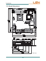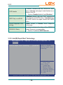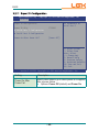
1
KR960
Mini-ITX Industrial Motherboard
User’s Manual
Version 1.0
2012.10
Index
Table of Contents
Chapter 1 - Introduction ............................................................................... 1
1.1 Copyright Notice ......................................................................... 2
1.2 Declaration of Conformity .......................................................... 2
1.3 About This User’s Manual .......................................................... 4
1.4 Warning ........................................................................................ 4
1.5 Replacing the Lithium Battery ................................................... 4
1.6 Technical Support ....................................................................... 5
1.7 Warranty ....................................................................................... 5
1.8 Packing List ................................................................................. 6
1.9 Ordering Information .................................................................. 6
1.10 Recommended CPU List........................................................... 6
............................................................................ 7
1.12 Installing the CPU...................................................................... 8
1.13 Board Dimensions..................................................................... 9
1.14 Installing the Memory ............................................................. 10
Chapter 2 - Installation ............................................................................... 11
2.1 Block Diagram ........................................................................... 12
2.2 Jumpers and Connectors ......................................................... 13
Jumpers ............................................................................................ 14
JPWR1: AT/ATX Power Mode Selection ...........................................14
JBAT1: Clear CMOS Setting..............................................................14
JRS1: COM2 RS-232 / 422 / 485 Selection .......................................14
CON1: COM3/4 Power Source Select on Pin 9................................15
JME1: ME Function Select ...............................................................15
Connectors ....................................................................................... 15
JSPI1: SPI Flash for External SPI Programming Tools ..................15
USB2: USB Port Connector ..............................................................15
INV1: LCD Inverter Connector ..........................................................16
COM1: RS-232 Connector .................................................................16
LVDS1: LVDS Connector ...................................................................16
AUDIO1: Audio Interface Port ...........................................................17
LAN1, 2: Ethernet Connectors (include USB0/1/2/3 Connector) ...17
USB1: 4 x USB Port Connector ........................................................18
DVI1: DVI-I Connector .......................................................................19
KBUSB1: PS/2 Keyboard and USB x 2 ............................................19
COM2: Serial Port Connector ...........................................................20
COM3~6: Serial Port Connectors .....................................................20
DIO1: DIO Port ....................................................................................20
12VIN1: ATX12V Connector ..............................................................21
-i-
Index
FAN1, 2: Fan Connectors ..................................................................21
JFRT1: Switches and Indicators ......................................................21
PWROUT1: SATA Power Connector .................................................21
SATA1~6: Serial ATA Connectors .....................................................22
LPC1: Low Pin Count Connector .....................................................22
MC1: Mini-card Slot ...........................................................................22
2.3 The Installation Paths of CD Driver ......................................... 24
Chapter 3 - BIOS ......................................................................................... 25
3.1 Main ............................................................................................ 26
3.2 Advanced ................................................................................... 28
3.2.1 ACPI Settings ...........................................................................29
3.2.2 S5 RTC Wake Settings.............................................................30
...................................................................31
.................................................................33
3.2.5 Intel(R) Rapid Start Technology .............................................36
.......................37
...................................................................38
...................................................................39
3.2.9 SMART Settings .......................................................................41
...........................................42
.........................................................43
3.2.12 H/W Monitor ............................................................................45
3.2.13 Intel(R) Smart Connect Technology .....................................46
........................................................47
3.3 Chipset ....................................................................................... 48
..............................................................49
..........................................54
3.4 Boot ............................................................................................ 61
3.4.1 CSM parameters ......................................................................62
3.5 Security ...................................................................................... 64
3.6 Save & Exit Options .................................................................. 65
3.7 AMI BIOS Checkpoints ............................................................. 66
3.7.1 Checkpoint Ranges .................................................................66
3.7.2 Standard Checkpoints .............................................................67
Appendix ..................................................................................................... 75
Appendix A: I/O Port Address Map ................................................ 76
Appendix B: BIOS Memory Map .................................................... 79
Appendix C: Interrupt Request Lines (IRQ) .................................. 81
Appendix D: Digital I/O Setting ...................................................... 82
Appendix E: Watchdog Timer (WDT) Setting................................ 91
- ii -
Introduction
1
Chapter 1
Introduction
Chapter 1 - Introduction
-1-
Introduction
1.1 Copyright Notice
All Rights Reserved.
The information in this document is subject to change without prior notice in
order to improve the reliability, design and function. It does not represent a
commitment on the part of the manufacturer.
Under no circumstances will the manufacturer be liable for any direct, indirect,
special, incidental, or consequential damages arising from the use or inability
to use the product or documentation, even if advised of the possibility of such
damages.
This document contains proprietary information protected by copyright.
All rights are reserved. No part of this manual may be reproduced by any
mechanical, electronic, or other means in any form without prior written
permission of the manufacturer.
1.2 Declaration of Conformity
CE
The CE symbol on your product indicates that it is in compliance with the
by contacting Technical Support.
shielded cables are used for external wiring. We recommend the use of
shielded cables. This kind of cable is available from Logic Supply. Please
contact your local supplier for ordering information.
conditions for passing included the equipment being operated within an
industrial enclosure. In order to protect the product from being damaged by
ESD (Electrostatic Discharge) and EMI leakage, we strongly recommend the
use of CE-compliant industrial enclosure products.
-2-
Introduction
FCC Class B
This device complies with Part 15 of the FCC Rules. Operation is subject to
the following two conditions:
(1)This device may not cause harmful interference, and
(2)This device must accept any interference received, including interference
that may cause undesired operation.
NOTE:
This equipment has been tested and found to comply with the limits for a
Class B digital device, pursuant to Part 15 of the FCC Rules. These limits
are designed to provide reasonable protection against harmful interference
in a residential installation. This equipment generates, uses and can radiate
radio frequency energy and, if not installed and used in accordance with
the instructions, may cause harmful interference to radio communications.
However, there is no guarantee that interference will not occur in a particular
installation. If this equipment does cause harmful interference to radio or
television reception, which can be determined by turning the equipment off
and on, the user is encouraged to try to correct the interference by one or
more of the following measures:
-- Reorient or relocate the receiving antenna.
-- Increase the separation between the equipment and receiver.
-- Connect the equipment into an outlet on a circuit different from that to
which the receiver is connected.
-- Consult the dealer or an experienced radio/TV technician for help.
RoHS
LGX Systems, certifies that all components in its products are in compliance
and conform to the European Union’s Restriction of Use of Hazardous
Substances in Electrical and Electronic Equipment (RoHS) Directive
2002/95/EC.
The above mentioned directive was published on 2/13/2003. The main purpose of the directive is to prohibit the use of lead, mercury, cadmium, hexavalent chromium, polybrominated biphenyls (PBB), and polybrominated diphenyl
ethers (PBDE) in electrical and electronic products. Member states of the EU
are to enforce by 7/1/2006.
LGX Systems hereby states that the listed products do not contain
-3-
Introduction
unintentional additions of lead, mercury, hex chrome, PBB or PBDB that exceed a maximum concentration value of 0.1% by weight or for cadmium exceed
as a substance or mixture of substances with uniform composition (such as solders, resins, plating, etc.). Lead-free solder is used for all terminations (Sn(9696.5%), Ag(3.0-3.5%) and Cu(0.5%)).
SVHC / REACH
To minimize the environmental impact and take more responsibility to the
of SVHC (Substances of Very High Concern) in (EC) 1907/2006 (REACH
--Registration, Evaluation, Authorization, and Restriction of Chemicals)
regulated by the European Union.
All substances listed in SVHC < 0.1 % by weight (1000 ppm)
1.3 About This User’s Manual
This user’s manual provides general information and installation instructions
about the product. This User’s Manual is intended for experienced users and
integrators with hardware knowledge of personal computers. If you are not
sure about any description in this booklet. please consult your vendor before
further handling.
1.4 Warning
Single Board Computers and their components contain very delicate
Integrated Circuits (IC). To protect the Single Board Computer and its
components against damage from static electricity, you should always follow
the following precautions when handling it :
1. Disconnect your Single Board Computer from the power source when you
want to work on the inside.
2. Hold the board by the edges and try not to touch the IC chips, leads or circuitry.
3. Use a grounded wrist strap when handling computer components.
4. Place components on a grounded antistatic pad or on the bag that comes
with the Single Board Computer, whenever components are separated from
the system.
1.5 Replacing the Lithium Battery
Incorrect replacement of the lithium battery may lead to a risk of explosion.
-4-
Introduction
The lithium battery must be replaced with an identical battery or a battery type
recommended by the manufacturer.
Do not throw lithium batteries into the trash-can. It must be disposed of in
accordance with local regulations concerning special waste.
1.6 Technical Support
customer service.
Phone: +1 802 861 7474
E-mail: [email protected]
1.7 Warranty
This product is warranted to be in good working order for a period of two years
from the date of purchase. Should this product fail to be in good working order
at any time during this period, we will, at our option, replace or repair it at no
additional charge except as set forth in the following terms. This warranty does
other incidental or consequential damage resulting from the use, misuse of,
or inability to use this product. Vendor will not be liable for any claim made by
any other related party.
Vendors disclaim all other warranties, either expressed or implied, including
particular purpose, with respect to the hardware, the accompanying product’s
manual(s) and written materials, and any accompanying hardware. This limited
Return authorization must be obtained from the vendor before returned
merchandise will be accepted. Authorization can be obtained by calling or
faxing the vendor and requesting a Return Merchandise Authorization (RMA)
number. Returned goods should always be accompanied by a clear problem
description.
-5-
Introduction
1.8 Packing List
Before you begin installing your single board, please make sure that the
following materials have been shipped:
1 x KR960 Mini-ITX industrial motherboard
1 x Driver CD
1 x Quick Installation Guide
1 x I/O Bracket
If any of the above items are damaged or missing, contact your vendor
immediately.
1.9 Ordering Information
KR960
Intel® Ivy Bridge rPGA988 socket Core™ i7/i5/i3,
Celeron® embedded Mini-ITX motherboard
CBK-KR960
Cable kit
2 x Two ports COM cables
1 x COM Flat cable
1.10 Recommended CPU List
Intel® 3rd Generation
i7-3610QE 2.3GHz Core™ Processor
i5-3610ME 2.7GHz Core™ Processor
i3-3120ME 2.4GHz Core™ Processor
Intel® 2nd Generation
i7-2710QE 2.1GHz Core™ Processor
i5-2510E 2.5GHz Core™ Processor
i3-2330E 2.2GHz Core™ Processor
B810 1.6GHz Celeron® Processor
-6-
1 x USB cable
2 x SATA cables
1 x SATA Power cable
Introduction
System
CPU
Support 3rd Generation Intel® Core™ i7/i5/i3
processors in rPGA988 (Socket G2)
Memory
2 x 204-pin DDR3 DIMM Sockets, supporting
1333/1600MHz SDRAM up to 16GB
Chipset
Intel® QM77
BIOS
AMI BIOS
Watchdog Timer
1~255 levels reset
I/O
I/O Chip
Fintek F71869ED + Fintek F81216AD
5 x RS-232 ports
Serial Port
control
USB Port
4 x USB 3.0/2.0 compatible ports
8 x USB 2.0 ports
KB/MS
1 x 6-pin wafer connector for PS/2 keyboard and
mouse
Digital I/O
1 x 16-bit programmable Digital Input/Output
Expansion Bus
Storage
Ethernet Chipset
Audio Interface
1 x PCIe x16 slot
1 x Mini-card slot
2 x Serial ATA ports with 600MB/s HDD transfer rate
4 x Serial ATA ports with 300MB/s HDD transfer rate
1 x Intel® 82579LM PCIe GbE PHY w/ iAMT
1 x Intel® 82583V PCIe GbE controller
Realtek ALC886 HD Audio Codec, Mic-in/Line-in/
Line-out
Display
Graphics Chipset
Integrated Intel HD Graphics 2500 or HD Graphics
4000
-7-
Introduction
Graphics Interface
1 x DVI-I connector, supporting either Analog RGB
or DVI, resolution up to 2048 x 1536 for Analog RGB
and 1920 x 1200 for TMDS
Support Dual Channel 24-bit LVDS up to 1600 x
1200 resolution
Mechanical & Environmental
Power Requirement DC12V input only
Power Consumption
4.3A@+12V with i7-3610QE (Typical)
Operating Temp.
-20 ~ 70°C (-4 ~ 158°F)
Operating Humidity
0 ~ 95% (non-condensing)
Dimensions (L x W) 170 x 170 mm (6.7" x 6.7")
1.12 Installing the CPU
The processor socket comes with a screw to secure the CPU. As shown in the
Place the CPU into the socket by making sure the notch on the corner of
the CPU correspond to the notch on the inside of the socket. Once the CPU
slides into the socket, lock the screw.
Make sure that heatsink is in complete contact with top surface of the CPU to
avoid the CPU’s overheating problem.
If not, it would cause your system or CPU to be hanged, unstable, damaged.
-8-
Introduction
1.13 Board Dimensions
Unit: mm
-9-
Introduction
1.14 Installing the Memory
To install the memory module:
1. Find the memory DIMM socket on the board.
The DIMM socket has a slot connector with a off-center break and two
place.
2. Position the memory module’s pin side at the SO-DIMM socket, with the
memory module’s key notch aligning at the SO-DIMM socket’s slot connector
break.
Lock
Lock
3. Insert the memory module to the slot connector at an slanted angle. Note to
“fully” insert the memory module to avoid improper insertion.
4. Press down the memory module until it auto-clicks in place.
To uninstall the memory module:
1. Pull back the latches from both sides of the SO-DIMM socket.
The memory module will be auto-released from the socket.
2. Remove the memory module.
- 10 -
Installation
2
Chapter 2
Installation
Chapter 2 - Installation
- 11 -
Installation
2.1 Block Diagram
Channel A
DDR3 1333/1600
Ivy Bridge
rPGA988B(non-ECC)
PCI-E x 16 SLOT
Channel B
PCI-E x 16
DMI2
(x4)
FDI
CH7318
DVI-I connector
DVI + CRT
DDI Port C
R, G, B output
Internal LVDS(18bit/24bit support)
DDR3 1333/1600
SATA 3.0 x2 / SATA 2.0 x4
Intel
Management
Engine
LVDS
PCI-E x1
2.5 GT/s
SPI
SPI Flash
USB 2.0
USB 2.0 (x12)
Intel 82579LM GbE PHY
LPC
Super I/O F71869ED
LAN1 (RJ-45 connector)
Mobile Intel QM77 Chipset
PS/2 x 1 (Y-Cable use)
PCI-E x1
2.5 GT/s
Intel 82583V GbE Controller
FAN1, FAN2 (smart fan control)
LAN2 (RJ-45 connector)
COM5 , COM6
2.5 GT/s
PCI-E MINI CARD
LPC1 debug port
ALC886 HD Audio
UART-F81216AD
Mic-in/Line-in/Line-out
COM1 RS232 w/ DB9 conn.
COM 2 RS232/422/485,
COM3, COM4 RS232
16-bit Digital I/O connector
SMBus
F75111RG
- 12 -
Installation
2.2 Jumpers and Connectors
27
24
FAN1
JFRT1
25
FAN2
35
PWROUT1
26
SATA2
SATA1
SATA4
28 SATA3
29
31
30
23
12VIN1 22
COM6 21
COM5 20
DIO1
19
CON1
COM4
COM2
COM3
18
SATA6
SATA5
32
JME1
1
JPWR1
2
JSPI1
3
JBAT1
4
USB2
6
LVDS1
MC1
33
17
16
15
5
34
JRS1
14
KBUSB1
13
12
11
DVI1
COM1
10
USB1
- 13 -
9
LAN1
8
LAN2
7
AUDIO1
INV1
LPC1
Installation
Jumpers
Jumper Settings
The jumper is “short” (closed) when the jumper cap is placed on pins. If not,
that means the jumper is “open.”
Pin open
Pin short
(closed)
Pin 2-3 short
(closed)
Pin 1-2 short
(closed)
JPWR1: AT/ATX Power Mode Selection (1)
Connector type: 2.00mm pitch 1x3-pin header.
Pin
Power Mode Selection
1-2
ATX Mode (Default)
2-3
AT Mode
3
2
1
3
2
1
JBAT1: Clear CMOS Setting (3)
Connector type: 2.00mm pitch 1x3-pin header.
Pin
Mode
1-2
Keep CMOS data (Default)
2-3
Clear CMOS data
3
2
1
3
2
1
JRS1: COM2 RS-232 / 422 / 485 Selection (14)
Connector type: 2.00mm pitch 2x4-pin header.
Assignment
Pin
RS-232 (Default) RS-422
RS-485
1-2
Short
Open
Open
3-4
Open
Short
Open
5-6
Open
Open
Short
7-8 **
Short
Short
Open/Short
** 485 Auto-Flow selection, Open: Enable, Short: Disable.
- 14 -
1 2
7 8
Installation
CON1: COM3/4 Power Source Select on Pin 9 (18)
Connector type: 2.00mm pitch 2x5-pin header.
Default setting: Standard
Pin 9 Power Source Special Support
COM3
CON1
COM4
CON1
Standard (RI) (Default)
7-9
8-10
POS: 12V/1A on Pin 9
1-3
2-4
POS: 5V/1A on Pin 9
3-5
4-6
1 2
9 10
JME1: ME Function Select (32)
Connector type: 2.00mm pitch 1x3-pin header.
Pin
Power Mode Selection
1-2
ME Enable/ME Flash disable (Default)
2-3
ME Disable/ME Flash enable
3
2
1
3
2
1
Connectors
JSPI1: SPI Flash for External SPI Programming Tools (2)
Connector type: 2.54mm pitch 2x4-pin header.
Pin Desc.
Pin Desc.
1 2
1
V_3P3_SPI
2
GND
3
SPI_CS0_R
4
SPI_CLK_R
5
SPI_SO_R
6
SPI_SI_R
7
NC
8
NC
7 8
USB2: USB Port Connector (4)
Connector type: 2.54mm pitch 2x5-pin header.
Pin Description
Pin Description
1 2
1
+5V
2
+5V
3
USBD2-
4
USBD3-
5
USBD2+
6
USBD3+
7
GND
8
GND
9
GND
10
N/C (Key)
9 10
- 15 -
Installation
INV1: LCD Inverter Connector (5)
Connector type: 2.00mm pitch 1x5 box wafer connector.
Pin Description
1
+12V
2
GND
3
Backlight on/off
4
Brightness control
5
GND
1
2
3
4
5
COM1: RS-232 Connector (11)
Connector type: D-sub 9-pin male connector.
Pin Desc.
Pin Desc.
1
DCD
6
DSR
2
RX
7
RTS
3
TX
8
CTS
4
DTR
9
RI
5
GND
10
NC
1
6
5
9
LVDS1: LVDS Connector (6)
Connector type: DF-13-34DP-1.25V connector.
Pin Description
Pin Description
2
VDD
1
VDD
4
TX2CLK+
3
TX1CLK+
6
TX2CLK-
5
TX1CLK-
8
GND
7
GND
10
TX2D0+
9
TX1D0+
12
TX2D0-
11
TX1D0-
14
GND
13
GND
16
TX2D1+
15
TX1D1+
- 16 -
2
1
30
29
Installation
18
TX2D1-
17
TX1D1-
20
GND
19
GND
22
TX2D2+
21
TX1D2+
24
TX2D2-
23
TX1D2-
26
GND
25
GND
28
TX2D3+
27
TX1D3+
30
TX2D3-
29
TX1D3-
AUDIO1: Audio Interface Port (7)
Connector type: triple stacked audio jacks (Stereo ø3.50).
Blue: Line In
Green: Line Out
Pink: MIC In
LAN1, 2: Ethernet Connectors (include USB0/1/2/3 Connector) (9, 8)
Connector type: RJ-45 + double stacked USB type A connector.
LAN (RJ-45)
Pin
Description
1
MDI0+
2
MDI0-
3
MDI1+
LED
4
MDI1-
5
MDI2+
6
MDI2-
7
MDI3+
8
MDI3-
LED
LAN
87654321
- 17 -
1 2 3 4
USB
1 2 3 4
USB
Installation
USB (USB type A connector)
Pin
Description
1
+5V
2
USB-
3
USB+
4
GND
USB1: 4 x USB Port Connector (10)
Connector type: 4-stack USB 3.0/2.0 type A connector.
Pin Desc.
Pin Desc.
11 5V
21 5V
12 USBD122 USBD213 USBD1+
23 USBD2+
14 GND1
24 GND3
15 SSRX125 SSRX216 SSRX1+
26 SSRX2+
17 GND2
27 GND4
18 SSTX128 SSTX219 SSTX1+
29 SSTX2+
31 5V
41 5V
32 USBD342 USBD433 USBD3+
43 USBD4+
34 GND5
44 GND7
35 SSRX345 SSRX436 SSRX3+
46 SSRX4+
37 GND6
47 GND8
38 SSTX348 SSTX439 SSTX3+
49 SSTX4+
H1 GND
H4 GND
H2 GND
H5 GND
H3 GND
H6 GND
- 18 -
Installation
DVI1: DVI-I Connector (12)
1
8
C1 C2
9
16
C5
17
24 C3 C4
Pin Description
Pin Description
Pin Description
1
TX2-
13
N.C.
C1
Analog RED
2
TX2+
14
+5V/50mA
C2
Analog Green
3
TX2/4GND
15
GND
C3
Analog Blue
4
N.C.
16
HTPLG
C4
Analog V_SYNC
5
N.C.
17
TX0-
C5
Analog R, G, B Return
6
DDC_CLK
18
TX0+
7
DDC_DATA
19
TX0/5GND
8
CRT_Vsync
20
N.C.
9
TX1-
21
N.C.
10
TX1+
22
TXC_GND
11
TX1/3GND
23
TXC+
12
N.C.
24
TXC-
KBUSB1: PS/2 Keyboard and USB x 2 (13)
Connector type: PS/2 Keyboard + USB connector.
Keyboard
(Purple)
MS_CLK
KB_VCC
MS_DAT
KB_CLK
KB_GND
KB_DAT
- 19 -
Installation
COM2: Serial Port Connector (16)
Connector type: 2.00mm pitch 2x7-pin box header.
Pin Desc.
Pin Desc.
1
DCD2
2
RXD2
3
TXD2
4
DTR2
5
GND
6
DSR2
7
RTS2
8
CTS2
9
RI2
10 NC
11
422TX+_485+
12 422TX-_485-
13
422RX+
14 422RX-
1 2
1314
COM3~6: Serial Port Connectors (15, 17, 20, 21)
Connector type: 2.00mm pitch 2x5-pin box header.
Pin Desc.
Pin
Desc.
1
DCD1
2
RXD1
3
TXD1
4
DTR1
5
GND
6
DSR1
7
RTS1
8
CTS1
9
RI1
10
NC
1 2
9 10
DIO1: DIO Port (19)
Connector type: 2.00mm pitch 2x10-pin header.
Pin Desc.
Pin Desc.
1
DIO0
2
DIO1
3
DIO2
4
DIO3
5
DIO4
6
DIO5
7
DIO6
8
DIO7
9
DIO8
10
DIO9
11
DIO10
12
DIO11
13
DIO12
14
DIO13
15
DIO14
16
DIO15
17
5V
18
GND
19
5V
20
GND
1 2
23 24
- 20 -
Installation
12VIN1: ATX12V Connector (22)
12INV1 supplies the CPU operation ATX +12V (Vcore).
Pin Description Pin Description
2
GND
1
GND
4
+12V
3
+12V
2
1
4
3
FAN1, 2: Fan Connectors (23, 25)
Connector type: 2.54mm pitch 1x4-pin wafer connector.
Pin
Description
1
1
GND
2
2
+12V
3
4
3
FAN_Detect
4
Control
JFRT1: Switches and Indicators (24)
It provides connectors for system indicators that provide light indication of
the computer activities and switches to change the computer status.
Connector type: 2.54mm pitch 2x5-pin header.
Pin
Description
Pin
Description
1
RESET+
2
RESET-
3
POWER_LED+
4
POWER_LED-
5
HDD_LED+
6
HDD_LED-
7
SPEAKER+
8
SPEAKER-
9
PSON+
10
PSON-
PWROUT1: SATA Power Connector (35)
Connector type: 2.50mm pitch 1x4-pin wafer connector.
Pin
Description
1
1
5V
2
2
GND
3
4
3
GND
4
12V_FAN2
- 21 -
1
9
2
10
Installation
SATA1~6: Serial ATA Connectors (26~31)
High speed transfer rates (150MB/s).
Pin Description
1
GND
2
TX+
3
TX-
4
GND
5
RX-
6
RX+
7
GND
1
7
LPC1: Low Pin Count Connector (34)
Connector type: CVILUX 0.5mm CF20141U0*0-LF connector.
Pin Desc.
Pin Desc.
1
LPC_D0
8
LPC_RST#
2
LPC_D1
9
GND
3
LPC_D2
10
LPC_CLK_33Mhz
4
LPC_D3
11
GND
5
GND
12
GND
6
LPC_FRAME#
13
+3.3V
7
SERIRQ
14
+3.3V
14
MC1: Mini-card Slot (33)
2
1
15
17
51
1
16
18
52
- 22 -
Installation
Pin
1
3
5
7
9
11
13
15
17
19
21
23
25
27
29
31
33
35
37
39
41
43
45
47
49
51
Desc.
Wake
COEX1
COEX2
CLKREQ#
GND
REFCLKREFCLK+
GND
UIM_C8/Reserved
UIM_C4/Reserved
GND
PERn0
PERp0
GND
GND
PETn0
PETp0
GND
GND
+3.3V
+3.3V
GND
Reserved
Reserved
Reserved
Reserved
Pin
2
4
6
8
10
12
14
16
18
20
22
24
26
28
30
32
34
36
38
40
42
44
46
48
50
52
Desc.
+3.3V
GND
+1.5V
UIM_PWR
UIM_DATA
UIM_CLK
UIM_RESET
UIM_VPP
GND
W_Disable#
PERST#
+3.3V
GND
+1.5V
SMB_CLK
SMB_DATA
GND
USB_DUSB_D+
GND
LED_WWAN#
LED_WLAN#
LED_WPAN#
+1.5V
GND
+3.3V
- 23 -
Installation
2.3 The Installation Paths of CD Driver
Windows 7
Driver
Path
CHIPSET
\KR960\CHIPSET\Win7
ME
\KR960\ME\MEI_allOS_8.0.4.1441_PV_5M
GRAPHICS
\KR960\GRAPHICS\Win7\Win32
\KR960\GRAPHICS\Win7\Win64
LAN
\KR960\ETHERNET\WIN_allos_Ver16.3
AUDIO
\KR960\AUDIO\Vista_Win7_R261-32_64 bit
USB3.0
\KR960\USB3.0
- 24 -
BIOS
3
Chapter 3
BIOS
Chapter 3 - BIOS
- 25 -
BIOS
3.1 Main
The AMI BIOS provides a Setup utility program for specifying the system
immediately activated. To enter the BIOS SETUP UTILITY, press “Delete”
once the power is turned on. When the computer is shut down, the battery on
the motherboard supplies the power for BIOS RAM.
The Main Setup screen lists the following information:
Aptio Setup Utility - Copyright (C) 2011 American Megatrends, Inc.
Main Advanced Chipset Boot Security Save & Exit
BIOS Information
BIOS Vendor
Core Version
Compliancy
Project version
Build Date and Time
American Megatrends
4.6.5.3
UEFI 2.3; PI 1.2
KR960 0.0.1 X64
06/28/2012 12:38:26
System Language
[English]
System Date
System Time
[Wed 10/03/2012]
[17:31:42]
Access Level
Administrator
Choose the system
default language
ȲȰ6HOHFW6FUHHQ
ȳȱ6HOHFW,WHP
Enter: Select
+/-: Change Opt.
F1: General Help
F2: Previous Values
F9: Optimized Defaults
F10: Save and Exit
ESC: Exit
Version 2.14.1219. Copyright (c) 2011 American Megatrendes, Inc.
Setting
Description
BIOS Information
BIOS Vendor
displays vendor name
Core Version
displays current core version information
Compliancy
displays compliant format
Project Version
displays current BIOS version information
Build Date and Time
the date that the BIOS version was made/updated
- 26 -
BIOS
System Language
Choose the system default language
System Date
Set the system date. Note that the ‘Day’ automatically changes when you set the date.
Ź The date format is: Day: Sun to Sat
Month: 1 to 12
Date: 1 to 31
Year: 1998 to 2099
System Time
Set the system time.
Ź The time format is: Hour: 00 to 23
Minute: 00 to 59
Second: 00 to 59
Key Commands
BIOS Setup Utility is mainly a key-based navigation interface. Please refer to
the following key command instructions for navigation process.
Keystroke
ŻŹ
źŸ
Function
the top menu bar / Move to highlight items on the screen
Move to highlight previous/next item
Enter
Esc
On the Main Menu – Quit the setup and not save
changes into CMOS (a message screen will display
and ask you to select “OK” or “Cancel” for exiting and
GLVFDUGLQJFKDQJHV8VH³ĸ´DQG³ĺ´WRVHOHFWDQGSUHVV
On the Sub Menu – Exit current page and return to main
menu
Page Up / +
Increase the numeric value on a selected setup item /
make change
Page Down -
Decrease the numeric value on a selected setup item /
make change
F1
F10
Activate “General Help” screen
Save the changes that have been made in the setup and
exit. (a message screen will display and ask you to select
³2.´RU³&DQFHO´IRUH[LWLQJDQGVDYLQJFKDQJHV8VH³ĸ´
- 27 -
BIOS
3.2 Advanced
of your hardware, such as ACPI, CPU, SATA, AMT, USB and (Second) Super
IO.
Aptio Setup Utility - Copyright (C) 2011 American Megatrends, Inc.
Main $GYDQFHG Chipset Boot Security 6DYH([LW
ɱ
ɱ
ɱ
ɱ
ɱ
ɱ
ɱ
ɱ
ɱ
ɱ
ɱ
ɱ
ɱ
ɱ
ACPI Settings
S5 RTC Wake Settings
CPU Configuration
SATA Configuration
Intel(R) Rapid Start Technology
Intel(R) Anti-Theft Technology Configuration
AMT Configuration
USB Configuration
SMART Settings
Second Super IO Configuration
Super IO Configuration
H/W Monitor
Intel(R) Smart Connect Technology
CPU PPM Configuration
System ACPI Parameters
ȲȰ6HOHFW6FUHHQ
ȳȱ6HOHFW,WHP
(QWHU6HOHFW
&KDQJH2SW
)*HQHUDO+HOS
)3UHYLRXV9DOXHV
)2SWLPL]HG'HIDXOWV
)6DYHDQG([LW
(6&([LW
Version 2.14.1219. Copyright (c) 2011 American Megatrendes, Inc.
Setting
Description
ACPI Settings
See Section 3.2.1
S5 RTC Wake Settings
See Section 3.2.2
See Section 3.2.3
See Section 3.2.4
Intel(R) Rapid Start Technology
See Section 3.2.5
See Section 3.2.6
See Section 3.2.7
See Section 3.2.8
SMART Settings
See Section 3.2.9
- 28 -
BIOS
See Section 3.2.10
See Section 3.2.11
H/W Monitor
See Section 3.2.12
Intel(R) Smart Connect Technology
See Section 3.2.13
See Section 3.2.14
3.2.1 ACPI Settings
Aptio Setup Utility - Copyright (C) 2011 American Megatrends, Inc.
Advanced
ACPI Settings
Enable Hibernation
ACPI Sleep State
Power-Supply Type
Enables or Disables
System ability to
Hibernate (OS/S4 Sleep
State). This option
[Enabled]
[Both S1 and S3 ava...] may be not effective
with some OS.
[ATX]
ȲȰ6HOHFW6FUHHQ
ȳȱ6HOHFW,WHP
(QWHU6HOHFW
&KDQJH2SW
)*HQHUDO+HOS
)3UHYLRXV9DOXHV
)2SWLPL]HG'HIDXOWV
)6DYHDQG([LW
(6&([LW
Version 2.14.1219. Copyright (c) 2011 American Megatrendes, Inc.
Setting
Enable Hibernation
Description
Enable (default) or Disable system ability to Hibernate (OS/S4 Sleep State). This option may be not
effective with some OS.
- 29 -
BIOS
ACPI Sleep State
Select ACPI sleep state the system will enter when
the SUSPEND button is pressed.
Ź Options: Suspend Disabled, S1 only(CPU
Stop Clock), S3 only(Suspend to RAM), Both
S1 and S3 available for OS to choose from
(default).
Power-Supply Type
Select Power-Supply Type.
Ź Options: AT, ATX (default).
3.2.2 S5 RTC Wake Settings
Enable system to wake from S5 using RTC alarm.
Aptio Setup Utility - Copyright (C) 2011 American Megatrends, Inc.
Advanced
Wake system with Fixed Time
[Disabled]
Wake system with Dynamic Time [Disabled]
Enable or disable
System wake on alarm
event. When enabled,
System will wake on
the hr::min::sec
specified
ȲȰ6HOHFW6FUHHQ
ȳȱ6HOHFW,WHP
Enter: Select
+/-: Change Opt.
F1: General Help
F2: Previous Values
F9: Optimized Defaults
F10: Save and Exit
ESC: Exit
Version 2.14.1219. Copyright (c) 2011 American Megatrendes, Inc.
Setting
Wake system with
Fixed Time
Description
Enable or Disable (default) System wake on alarm
event. When enabled, System will wake on the
- 30 -
BIOS
Wake system with
Dynamic Time
Enable or Disable (default) System wake on alarm
event. When enabled, System will wake on the current time + Increase minute(s).
Aptio Setup Utility - Copyright (C) 2011 American Megatrends, Inc.
Advanced
CPU Configuration
Intel(R) Core(TM) i7-3610QE CPU @ 2.30GHz
306a8
CPU Signature
10
Microcode Patch
2300 MHz
Max CPU Speed
1200 MHz
Min CPU Speed
2300 MHz
CPU Speed
4
Processor Cores
Supported
Intel HT Technology
Supported
Intel VT-x Technology
Supported
Intel SMX Technology
Supported
64-bit
L1
L1
L2
L3
Data Cache
Code Cache
Cache
Cache
Hyper-threading
Active Processor Cores
Limit CPUID Maximum
Execute Disable Bit
Intel Virtualization Technology
Hardware Prefetcher
Adjacent Cache Line Prefetch
32 KB x 4
32 KB x 4
256 KB x 4
6144 KB
To turn on/off
prefetching of
adjacent cache lines.
ȲȰ6HOHFW6FUHHQ
ȳȱ6HOHFW,WHP
(QWHU6HOHFW
&KDQJH2SW
)*HQHUDO+HOS
)3UHYLRXV9DOXHV
)2SWLPL]HG'HIDXOWV
)6DYHDQG([LW
(6&([LW
[Enabled]
[All]
[Disabled]
[Enabled]
[Disabled]
[Enabled]
[Enabled]
Version 2.14.1219. Copyright (c) 2011 American Megatrendes, Inc.
- 31 -
BIOS
Setting
Description
Hyper-threading
Enabled (default) for Windows XP and Linux (OS
optimized for Hyper-threading Technology) and
Disabled for other OS (OS not optimized for Hyper-threading Technology).
When Disabled, only one thread per enabled core
is enabled.
Active Processor
Cores
Number of cores to enable in each processor
package.
Ź Options: All (default), 1, 2, 3
Limit CPUID Maximum
Disabled for Windows XP
Ź Options: Enabled and Disabled (default).
Execute Disable Bit
XP can prevent certain classes of malicious buffer
ing OS (Windows Server 2003 SP1, Windows XP
SP2, SuSE Linux 9.2, RedHat Enterprise 3 Update
3.)
Ź Options: Enabled (default) and Disabled.
Intel Virtualization
Technology
When enabled, a VMM can utilize the additional
hardware capabilities provided by Vanderpool
Technology.
Ź Options: Enabled and Disabled (default).
Hardware Prefetcher
To turn on/off the Mid Level Cache (L2) streamer
prefetcher.
Ź Options: Enabled (default) and Disabled.
Adjacent Cache Line
Prefetch
To turn on/off prefetching of adjacent cache lines.
Ź Options: Enabled (default) and Disabled.
- 32 -
BIOS
Aptio Setup Utility - Copyright (C) 2011 American Megatrends, Inc.
$GYDQFHG
[Enabled]
SATA Controller(s)
>$+&,@
SATA Mode Selection
>*HQ@
SATA Controller Speed
ɱ6RIWZDUH)HDWXUH0DVN&RQILJXUDWLRQ
6HULDO$7$3RUW
6RIWZDUH3UHVHUYH
3RUW
+RW3OXJ
([WHUQDO6$7$
6$7$'HYLFH7\SH
6SLQ8S'HYLFH
6HULDO$7$3RUW
6RIWZDUH3UHVHUYH
3RUW
+RW3OXJ
([WHUQDO6$7$
6$7$'HYLFH7\SH
6SLQ8S'HYLFH
6HULDO$7$3RUW
6RIWZDUH3UHVHUYH
3RUW
+RW3OXJ
([WHUQDO6$7$
6$7$'HYLFH7\SH
6SLQ8S'HYLFH
6HULDO$7$3RUW
6RIWZDUH3UHVHUYH
3RUW
+RW3OXJ
([WHUQDO6$7$
6$7$'HYLFH7\SH
6SLQ8S'HYLFH
6HULDO$7$3RUW
6RIWZDUH3UHVHUYH
3RUW
+RW3OXJ
([WHUQDO6$7$
6$7$'HYLFH7\SH
6SLQ8S'HYLFH
6HULDO$7$3RUW
6RIWZDUH3UHVHUYH
3RUW
+RW3OXJ
([WHUQDO6$7$
6$7$'HYLFH7\SH
6SLQ8S'HYLFH
(QDEOHRU'LVDEOH6$7$
'HYLFH
Empty
8QNQRZQ
[Enabled]
>'LVDEOHG@
>'LVDEOHG@
>+DUG'LVN'ULYHU@
>'LVDEOHG@
Empty
8QNQRZQ
[Enabled]
>'LVDEOHG@
>'LVDEOHG@
>+DUG'LVN'ULYHU@
>'LVDEOHG@
Empty
8QNQRZQ
[Enabled]
>'LVDEOHG@
>'LVDEOHG@
>'LVDEOHG@
>'LVDEOHG@
Empty
8QNQRZQ
[Enabled]
>'LVDEOHG@
>'LVDEOHG@
>'LVDEOHG@
>'LVDEOHG@
Empty
8QNQRZQ
[Enabled]
>'LVDEOHG@
>'LVDEOHG@
>'LVDEOHG@
>'LVDEOHG@
Empty
8QNQRZQ
[Enabled]
>'LVDEOHG@
>'LVDEOHG@
>'LVDEOHG@
>'LVDEOHG@
ȲȰ6HOHFW6FUHHQ
ȳȱ6HOHFW,WHP
(QWHU6HOHFW
&KDQJH2SW
)*HQHUDO+HOS
)3UHYLRXV9DOXHV
)2SWLPL]HG'HIDXOWV
)6DYHDQG([LW
(6&([LW
Version 2.14.1219. Copyright (c) 2011 American Megatrendes, Inc.
- 33 -
BIOS
Setting
Description
SATA Controller(s)
Enable (default) or Disable SATA Device.
SATA Mode Selection
Determine how SATA controller(s) operate.
Ź Options: IDE, AHCI (default) and RAID.
SATA Controller
Speed
Indicates the maximum speed the SATA controller
can support.
Ź Options: Gen1, Gen2, Gen3 (default)
Software Feature
Port 0~5
Enable (default) or Disable SATA Port.
Hot Plug
Designates this port as Hot Pluggable.
Ź Options: Enabled and Disabled (default).
External SATA
External SATA Support.
Ź Options: Enabled and Disabled (default).
SATA Device Type
Identify the SATA port is connected to Solid State
Drive or Hard Disk Drive.
Ź Options: Hard Disk Driver (default) and Solid
State Drive.
Spin Up Device
On an edge detect from 0 to 1, the PCH starts a
COMRESET initialization sequence to the device.
Ź Options: Enabled and Disabled (default).
- 34 -
BIOS
Aptio Setup Utility - Copyright (C) 2011 American Megatrends, Inc.
$GYDQFHG
5$,'
[Enabled]
5$,'
[Enabled]
5$,'
[Enabled]
5$,'
[Enabled]
,QWHO5DSLG5HFRYHU\7HFKQRORJ\ [Enabled]
25208,DQG%$11(5
[Enabled]
+''8QORFN
[Enabled]
[Enabled]
/('/RFDWH
[Enabled]
,5572QO\RQH6$7$
6PDUW5HVSRQVH7HFKQRORJ\
[Enabled]
25208,'HOD\
[2 Seconds]
Enable or disable
5$,'IHDWXUH
ȲȰ6HOHFW6FUHHQ
ȳȱ6HOHFW,WHP
(QWHU6HOHFW
&KDQJH2SW
)*HQHUDO+HOS
)3UHYLRXV9DOXHV
)2SWLPL]HG'HIDXOWV
)6DYHDQG([LW
(6&([LW
Version 2.14.1219. Copyright (c) 2011 American Megatrendes, Inc.
Setting
Description
RAID0/1/10/5
Enable (default) or Disable RAID0/1/10/5 feature.
Intel Rapid Recovery
Technology
Enable (default) or Disable Intel Rapid Recovery Technology.
If enabled, then the OROM UI is shown. Otherwise, no OROM banner or information will be disOROM UI and BANNER
played if all disks and RAID volumes are Normal.
Ź Options: Enabled (default) and Disabled.
HDD Unlock
If enabled, indicates that the HDD password unlock in the OS is enabled.
Ź Options: Enabled (default) and Disabled.
- 35 -
BIOS
LED Locate
If enabled, indicates that the LED/SGPIO hardware is attached and ping to locate feature is enabled on the OS.
Ź Options: Enabled (default) and Disabled.
IRRT Only on eSATA
If enabled (default), then only IRRT volumes can
span internal and eSATA drives. If disabled, then
any RAID volume can span internal and eSATA
drives.
Smart Response Technology
Enable (default) or Disable Smart Response
Technology.
OROM UI Delay
If enabled, indicates the delay of the OROM UI
Splash Screen in a normal status.
Ź Options: 2 (default) /4/6/8 Seconds
3.2.5 Intel(R) Rapid Start Technology
Aptio Setup Utility - Copyright (C) 2011 American Megatrends, Inc.
$GYDQFHG
Intel(R) Rapid Start Technology
>'LVDEOHG@
(QDEOHRUGLVDEOH
Intel(R) Rapid Start
Technology.
ȲȰ6HOHFW6FUHHQ
ȳȱ6HOHFW,WHP
(QWHU6HOHFW
&KDQJH2SW
)*HQHUDO+HOS
)3UHYLRXV9DOXHV
)2SWLPL]HG'HIDXOWV
)6DYHDQG([LW
(6&([LW
Version 2.14.1219. Copyright (c) 2011 American Megatrendes, Inc.
- 36 -
BIOS
Setting
Intel(R) Rapid Start
Technology
Description
Enable or Disable (default) Intel(R) Rapid Start
Technology.
Disabling Intel(R) AT allows User to login to platform. This is strictly for testing
only. This does not disable Intel(R) AT Services in ME.
Aptio Setup Utility - Copyright (C) 2011 American Megatrends, Inc.
$GYDQFHG
,QWHO5$QWL7KHIW7HFKQRORJ\&RQILJXUDWLRQ
,QWHO5$QWL7KHIW7HFKQRORJ\
,QWHO5$QWL7KHIW7HFKQRORJ\5HF
Enter Intel(R) AT Suspend Mode
[Enabled]
3
>'LVDEOHG@
(QDEOH'LVDEOH,QWHO
5$7LQ%,26IRU
testing only.
ȲȰ6HOHFW6FUHHQ
ȳȱ6HOHFW,WHP
(QWHU6HOHFW
&KDQJH2SW
)*HQHUDO+HOS
)3UHYLRXV9DOXHV
)2SWLPL]HG'HIDXOWV
)6DYHDQG([LW
(6&([LW
Version 2.14.1219. Copyright (c) 2011 American Megatrendes, Inc.
Setting
Description
Intel(R) Anti-Theft
Technology
Enable or Disable (default) Intel(R) AT in BIOS for
testing only.
Intel(R) Anti-Theft
Technology Rec
Set the number of times Recovery attempted will be
allowed.
- 37 -
BIOS
Aptio Setup Utility - Copyright (C) 2011 American Megatrends, Inc.
Advanced
[Enabled]
Intel AMT
Activate Remote Assistance Process [Disabled]
0
AMT CIRA Timeout
Enable/Disable Intel
(R) Active Management
Technology BIOS
Extension. Note:
iAMT H/W is always
enabled. This option
just controls the BIOS
extension execution.If
enabled, this requires
additional firmware
in the SPI device
ȲȰ6HOHFW6FUHHQ
ȳȱ6HOHFW,WHP
Enter: Select
+/-: Change Opt.
F1: General Help
F2: Previous Values
F9: Optimized Defaults
F10: Save and Exit
ESC: Exit
Version 2.14.1219. Copyright (c) 2011 American Megatrendes, Inc.
Setting
Intel AMT
Description
Enable (default) or Disable Intel (R) Active Management Technology BIOS Extension.
Note: iAMT H/W is always enabled.
This option just controls the BIOS extension executhe SPI device
Activate Remote
Assistance Process
Trigger CIRA boot.
Ź Options: Enabled and Disabled (default).
- 38 -
BIOS
Aptio Setup Utility - Copyright (C) 2011 American Megatrends, Inc.
Advanced
USB Configuration
USB Devices:
1 Keyboard, 1 Mouse, 2 Hubs
Legacy USB Support
USB3.0 Support
XHCI Hand-off
EHCI Hand-off
USB Beep Switch
[Enabled]
[Enabled]
[Enabled]
[Disabled]
[Enabled]
USB hardware delays and time-outs:
USB transfer time-out
[20 sec]
Device reset time-out
[20 sec]
Device power-up delay
[Auto]
Enables Legacy USB
support. AUTO option
disables legacy
support if no USB
devices are connected.
DISABLE option will
keep USB devices
available only for EFI
applications.
ȲȰ6HOHFW6FUHHQ
ȳȱ6HOHFW,WHP
Enter: Select
+/-: Change Opt.
F1: General Help
F2: Previous Values
F9: Optimized Defaults
F10: Save and Exit
ESC: Exit
Version 2.14.1219. Copyright (c) 2011 American Megatrendes, Inc.
Setting
Description
USB Devices:
Legacy USB Support
Enables (default) Legacy USB support. AUTO option disables legacy support if no USB devices are
connected. DISABLE option will keep USB devices available only for EFI applications.
USB3.0 Support
Enable (default) or Disable USB3.0 (XHCI) Controller support.
XHCI Hand-off
This is a workaround for OSes without XHCI handoff support. The XHCI ownership change should
be claimed by XHCI driver.
Ź Options: Enabled (default) and Disabled.
- 39 -
BIOS
EHCI Hand-off
This is a workaround for OSes without EHCI handoff support. The EHCI ownership change should
be claimed by EHCI driver.
Ź Options: Enabled and Disabled (default).
USB Beep Switch
Enable (default) or Disable USB Beep sound.
USB hardware delays and time-outs:
USB transfer time-out
The time-out value for Control, Bulk, and Interrupt
transfers.
Ź Options: 1/5/10/20 sec (default)
Device reset time-out
USB mass storage device Start Unit command
time-out.
Ź Options: 10/20 (default)/30/40 sec
Maximum time the device will take before it properly reports itself to the host controller. ‘Auto’ uses
Device power-up delay default value: for a Root port it is 100ms, for a
Hub port the delay is taken from hub descriptor.
Ź Options: Auto (default) and Manual
- 40 -
BIOS
3.2.9 SMART Settings
Aptio Setup Utility - Copyright (C) 2011 American Megatrends, Inc.
$GYDQFHG
SMART Settings
60$576HOI7HVW
5XQ60$576HOI7HVWRQ
DOO+''VGXULQJ3267
>'LVDEOHG@
ȲȰ6HOHFW6FUHHQ
ȳȱ6HOHFW,WHP
(QWHU6HOHFW
&KDQJH2SW
)*HQHUDO+HOS
)3UHYLRXV9DOXHV
)2SWLPL]HG'HIDXOWV
)6DYHDQG([LW
(6&([LW
Version 2.14.1219. Copyright (c) 2011 American Megatrendes, Inc.
Setting
SMART Self Test
Description
Run SMART Self Test on all HDDs during POST.
Ź Options: Enabled and Disabled (default).
- 41 -
BIOS
Aptio Setup Utility - Copyright (C) 2011 American Megatrends, Inc.
$GYDQFHG
6HFRQG6XSHU,2&RQILJXUDWLRQ
6XSHU,2&KLS
ɱ6HULDO3RUW&RQILJXUDWLRQ
ɱ6HULDO3RUW&RQILJXUDWLRQ
ɱ6HULDO3RUW&RQILJXUDWLRQ
ɱ6HULDO3RUW&RQILJXUDWLRQ
6HW3DUDPHWHUVRI
6HULDO3RUW&20$
Fintek F81216
ȲȰ6HOHFW6FUHHQ
ȳȱ6HOHFW,WHP
(QWHU6HOHFW
&KDQJH2SW
)*HQHUDO+HOS
)3UHYLRXV9DOXHV
)2SWLPL]HG'HIDXOWV
)6DYHDQG([LW
(6&([LW
Version 2.14.1219. Copyright (c) 2011 American Megatrendes, Inc.
- 42 -
BIOS
Aptio Setup Utility - Copyright (C) 2011 American Megatrends, Inc.
$GYDQFHG
6HW3DUDPHWHUVRI
6HULDO3RUW
6XSHU,2&RQILJXUDWLRQ
6XSHU,2&KLS
ɱ6HULDO3RUW&RQILJXUDWLRQ
ɱ6HULDO3RUW&RQILJXUDWLRQ
)(
3RZHU2Q$IWHU3RZHU)DLO
>3RZHU2II@
ȲȰ6HOHFW6FUHHQ
ȳȱ6HOHFW,WHP
(QWHU6HOHFW
&KDQJH2SW
)*HQHUDO+HOS
)3UHYLRXV9DOXHV
)2SWLPL]HG'HIDXOWV
)6DYHDQG([LW
(6&([LW
Version 2.14.1219. Copyright (c) 2011 American Megatrendes, Inc.
Setting
Power On After
Power Fail
Description
Specify what state to go to when power is re-applied
after a power failure.
Ź Options: Power Off (default) and Power On
- 43 -
BIOS
Aptio Setup Utility - Copyright (C) 2011 American Megatrends, Inc.
Advanced
Enable or Disable
Serial Port (COM)
Serial Port 1 Configuration
Serial Port
Device Settings
[Enabled]
IO=3F8h; IRQ=4;
Change Settings
[Auto]
ȲȰ6HOHFW6FUHHQ
ȳȱ6HOHFW,WHP
(QWHU6HOHFW
&KDQJH2SW
)*HQHUDO+HOS
)3UHYLRXV9DOXHV
)2SWLPL]HG'HIDXOWV
)6DYHDQG([LW
(6&([LW
Version 2.14.1219. Copyright (c) 2011 American Megatrendes, Inc.
Setting
Description
Serial Port
Enable (default) or Disable Serial Port (COM)
Change Settings
Select an optimal setting for Super IO device.
- 44 -
BIOS
3.2.12 H/W Monitor
Aptio Setup Utility - Copyright (C) 2011 American Megatrends, Inc.
$GYDQFHG
>$XWR)DQE\3:0'XW\@
&38)$10RGHVHWWLQJ
&387HPSHUDWXUH/LPLWRI+LJKHVW
&387HPSHUDWXUH/LPLWRI/RZHVW
40
&38)DQ+LJKHVW6HWWLQJ
100
&38)DQ6HFRQG6HWWLQJ
&38)DQ/RZHVW6HWWLQJ
30
System Fan Mode setting >$XWR)DQE\3:0'XW\@
System 7HPSHUDWXUH/LPLWRI+LJK
System 7HPSHUDWXUH/LPLWRI/RZH
40
System Fan +LJKHVW6HWWLQJ
100
System Fan Second Setting
System Fan /RZHVW6HWWLQJ
30
3F+HDOWK6WDWXV
&387HPSHUDWXUH
6\VWHP7HPSHUDWXUH
&38)$16SHHG
6<6)$16SHHG
Vcore
+5V
+1.5V
+12V
+3.3V
9%$7
°c
°c
530
1$
9
9
9
9
9
9
)$1&RQWURO0RGH
setting
ȲȰ6HOHFW6FUHHQ
ȳȱ6HOHFW,WHP
(QWHU6HOHFW
&KDQJH2SW
)*HQHUDO+HOS
)3UHYLRXV9DOXHV
)2SWLPL]HG'HIDXOWV
)6DYHDQG([LW
(6&([LW
Version 2.14.1219. Copyright (c) 2011 American Megatrendes, Inc.
Setting
CPU/System FAN Mode
setting
Description
Fan Control Mode Setting
Ź Options: Manual Duty Mode and Auto
Fan by PWM Duty (default).
CPU/System Temperature Highest Temperature Setting.
Limit of Highest
Min=0 Max=127 Please input Dec number:
CPU/System Temperature Lowest Temperature Setting.
Limit of Lowest
Min=0 Max=127 Please input Dec number:
CPU/System Fan Highest
Setting
Highest Speed Value
Min=0 Max=100 Please input Dec number:
- 45 -
BIOS
CPU/System Fan Second
Setting
Second Speed Value
Min=0 Max=100 Please input Dec number:
CPU/System Fan Lowest
Setting
Lowest Speed Value
Min=0 Max=100 Please input Dec number:
3.2.13 Intel(R) Smart Connect Technology
Aptio Setup Utility - Copyright (C) 2011 American Megatrends, Inc.
$GYDQFHG
,6&7&RQILJXUDWLRQ
>'LVDEOHG@
(QDEOH'LVDEOH,6&7
&RQILJXUDWLRQ
ȲȰ6HOHFW6FUHHQ
ȳȱ6HOHFW,WHP
(QWHU6HOHFW
&KDQJH2SW
)*HQHUDO+HOS
)3UHYLRXV9DOXHV
)2SWLPL]HG'HIDXOWV
)6DYHDQG([LW
(6&([LW
Version 2.14.1219. Copyright (c) 2011 American Megatrendes, Inc.
Setting
Description
Enable or Disable
- 46 -
BIOS
Aptio Setup Utility - Copyright (C) 2011 American Megatrends, Inc.
$GYDQFHG
&38330&RQILJXUDWLRQ
(QDEOH'LVDEOH,QWHO
SpeedStep
EIST
Turbo Mode
&38&5HSRUW
&38&5HSRUW
&38&5HSRUW
&RQILJ7'3/2&.
/RQJGXUDWLRQSRZHUOLPLW
/RQJGXUDWLRQPDLQWDLQHG
6KRUWGXUDWLRQSRZHUOLPLW
$&3,76WDWH
[Enabled]
[Enabled]
[Enabled]
[Enabled]
[Enabled]
>'LVDEOHG@
0
1
0
>'LVDEOHG@
ȲȰ6HOHFW6FUHHQ
ȳȱ6HOHFW,WHP
(QWHU6HOHFW
&KDQJH2SW
)*HQHUDO+HOS
)3UHYLRXV9DOXHV
)2SWLPL]HG'HIDXOWV
)6DYHDQG([LW
(6&([LW
Version 2.14.1219. Copyright (c) 2011 American Megatrendes, Inc.
Setting
Description
EIST
Enable (default) or Disable Intel SpeedStep
Turbo Mode
Enable (default) or Disable Turbo Mode
CPU C3 Report
Enable (default) or Disable CPU C3(ACPI C2)
report to OS
CPU C6 Report
Enable (default) or Disable CPU C6(ACPI C3)
report to OS
CPU C7 Report
Enable (default) or Disable CPU C7(ACPI C3)
report to OS
Ź
Long duration power limit
Options: Enabled and Disabled (default)
Long duration power limit in Watts, 0 means use
factory default.
- 47 -
BIOS
Long duration maintained
Time window which the long duration power is
maintained.
Short duration power limit
Short duration power limit in watts, 0 means use
factory default.
ACPI T State
Enable or Disable (default) ACPI T state support
3.3 Chipset
Aptio Setup Utility - Copyright (C) 2011 American Megatrends, Inc.
Main Advanced Chipset Boot Security Save & Exit
PCH Parameters
ɱ3&+,2&RQILJXUDWLRQ
ɱ6\VWHP$JHQW6$&RQILJXUDWLRQ
ȲȰ6HOHFW6FUHHQ
ȳȱ6HOHFW,WHP
(QWHU6HOHFW
&KDQJH2SW
)*HQHUDO+HOS
)3UHYLRXV9DOXHV
)2SWLPL]HG'HIDXOWV
)6DYHDQG([LW
(6&([LW
Version 2.14.1219. Copyright (c) 2011 American Megatrendes, Inc.
Setting
Description
See Section 3.3.1
See Section 3.3.2
- 48 -
BIOS
Aptio Setup Utility - Copyright (C) 2011 American Megatrends, Inc.
Chipset
,QWHO3&+5&9HUVLRQ
,QWHO3&+6.81DPH
,QWHO3&+5HY,'
1.2.0.1
QM77
04/C1
PCI Express
Configuration settings
ɱ 3&+([SUHVV&RQILJXUDWLRQ
ɱ USB Configuration
3&+/$1&RQWUROOHU
:DNHRQ/$1
[Enabled]
[Enabled]
+LJK3UHFLVLRQ(YHQW7LPHU&RQILJXUDWLRQ
[Enabled]
+LJK3UHFLVLRQ7LPHU
6/3B6$VVHUWLRQ:LGWK
[4-5 Seconds]
ȲȰ6HOHFW6FUHHQ
ȳȱ6HOHFW,WHP
(QWHU6HOHFW
&KDQJH2SW
)*HQHUDO+HOS
)3UHYLRXV9DOXHV
)2SWLPL]HG'HIDXOWV
)6DYHDQG([LW
(6&([LW
Version 2.14.1219. Copyright (c) 2011 American Megatrendes, Inc.
Setting
Description
PCH LAN Controller
Enable (default) or Disable onboard NIC.
Wake on LAN
Enable (default) or Disable integrated LAN to
wake the system. (The Wake On LAN cannot
be disabled if ME is on at Sx state.)
High Precision Timer
Enable (default) or Disable the High Precision Event Timer.
SLP_S4 Assertion Width
Select a minimum assertion width of the SLP_
S4# signal.
Ź Options: Disabled (default), 1-2/2-3/34/4-5 Seconds
- 49 -
BIOS
Aptio Setup Utility - Copyright (C) 2011 American Megatrends, Inc.
Chipset
PCI Express Configuration
PCI Express Clock Gating
'0,/LQN$630&RQWURO
'0,/LQN([WHQGHG6\QFK&RQWURO
PCIe-USB Glitch W/A
6XEWUDFWLYH'HFRGH
[Enabled]
[Enabled]
>'LVDEOHG@
>'LVDEOHG@
>'LVDEOHG@
3&,(3RUWLVDVVLJQHGWR/$1
ɱ PCI Express Root Port 2
ɱ PCI Express Root Port 3
Enable or disable PCI
Express Clock Gating
for each root port.
ȲȰ6HOHFW6FUHHQ
ȳȱ6HOHFW,WHP
(QWHU6HOHFW
&KDQJH2SW
)*HQHUDO+HOS
)3UHYLRXV9DOXHV
)2SWLPL]HG'HIDXOWV
)6DYHDQG([LW
(6&([LW
Version 2.14.1219. Copyright (c) 2011 American Megatrendes, Inc.
Setting
Description
PCI Express Clock
Gating
Enable (default) or Disable PCI Express Clock Gating for each root port.
DMI Link ASPM
Control
The control of Active State Power Management on
both NB side and SB side of the DMI Link.
Ź Options: Enabled (default) and Disabled.
DMI Link Extended
Synch Control
The control of Extended Synch on SB side of the
DMI Link.
Ź Options: Enabled and Disabled (default).
PCIe-USB Glitch
W/A
PCIe-USB Glitch W/A for bad USB devices connected behind PCIE/PEG Port.
Ź Options: Enabled and Disabled (default).
Subtractive Decode
Enable or Disable (default) PCI Express Subtractive
Decode.
- 50 -
BIOS
Aptio Setup Utility - Copyright (C) 2011 American Megatrends, Inc.
Chipset
PCI Express Root Port 2
ASPM Support
URR
FER
NFER
CER
&72
SEFE
SENFE
SECE
PME SCI
+RW3OXJ
PCIe Speed
([WUD%XV5HVHUYHG
5HVHUYHG0HPRU\
3UHIHWFKDEOH0HPRU\
5HVHUYHG,2
>(QDEOHG@
>$XWR@
>'LVDEOHG@
>'LVDEOHG@
>'LVDEOHG@
>'LVDEOHG@
>'LVDEOHG@
>'LVDEOHG@
>'LVDEOHG@
>'LVDEOHG@
>(QDEOHG@
>'LVDEOHG@
>$XWR@
0
10
10
4
Control the PCI
Express Root Port.
ȲȰ6HOHFW6FUHHQ
ȳȱ6HOHFW,WHP
(QWHU6HOHFW
&KDQJH2SW
)*HQHUDO+HOS
)3UHYLRXV9DOXHV
)2SWLPL]HG'HIDXOWV
)6DYHDQG([LW
(6&([LW
Version 2.14.1219. Copyright (c) 2011 American Megatrendes, Inc.
Setting
PCI Express Root
Port 2/3
Description
Control the PCI Express Root Port.
Ź Options: Enabled (default) and Disabled.
Set the ASPM Level:
Force L0 - Force all links to L0 State;
ASPM Support
DISABLE - Disable ASPM
Ź Options: Disabled, L0s, L1, L0sL1, Auto
(default)
URR
Enable or Disable (default) PCI Express Unsupported Request Reporting.
FER
Enable or Disable (default) PCI Express Device Fatal Error Reporting.
NFER
Enable or Disable (default) PCI Express Device
Non-Fatal Error Reporting.
- 51 -
BIOS
CER
Enable or Disable (default) PCI Express Device
Correctable Error Reporting.
CTO
Enable or Disable (default) PCI Express Completion Timer TO.
SEFE
Enable or Disable (default) Root PCI Express System Error on Fatal Error.
SENFE
Enable or Disable (default) Root PCI Express System Error on Non-Fatal Error.
SECE
Enable or Disable (default) Root PCI Express System Error on Correctable Error.
PME SCI
Enable (default) or Disable PCI Express PME SCI.
Hot Plug
Enable or Disable (default) PCI Express Hot Plug.
PCIe Speed
Select PCI Express port speed.
Ź Options: Auto (default), Gen1, Gen2
Extra Bus Reserved
Extra Bus Reserved (0~7) for bridges behind this
Root Bridge.
Reserved Memory
Reserved Memory (1~20) Range for this Root
Bridge.
Prefetchable Memory
Prefetchable Memory (1~20) Range for this Root
Bridge.
Reserved I/O
Reserved I/O (4k/8k/12k/16k/20k) Range for this
Root Bridge.
- 52 -
BIOS
Aptio Setup Utility - Copyright (C) 2011 American Megatrends, Inc.
Chipset
86%&RQILJXUDWLRQ
XHCI Pre-Boot Driver
[+&,0RGH
HS Port #1 Switchable
HS Port #2 Switchable
HS Port #3 Switchable
HS Port #4 Switchable
[+&,6WUHDPV
[Enabled]
[Smart Auto]
[Enabled]
[Enabled]
[Enabled]
[Enabled]
[Enabled]
EHCI1
[Enabled]
EHCI2
[Enabled]
USB Ports Per-Port Disable Control [Disabled]
Enable or disable XHCI
Pre-Boot Driver
support.
ȲȰ6HOHFW6FUHHQ
ȳȱ6HOHFW,WHP
(QWHU6HOHFW
&KDQJH2SW
)*HQHUDO+HOS
)3UHYLRXV9DOXHV
)2SWLPL]HG'HIDXOWV
)6DYHDQG([LW
(6&([LW
Version 2.14.1219. Copyright (c) 2011 American Megatrendes, Inc.
Setting
Description
XHCI Pre-Boot Driver
Enable (default) or Disable XHCI Pre-Boot Driver
support.
xHCI Mode
Mode of operation of xHCI controller.
Ź Options: Smart Auto (default), Auto, Enabled,
Disabled
HS Port #1/2/3/4
Switchable
Always for HS port switching between xHCI and
EHCI. If disabled, port is routed to EHCI. If HS
port is routed to xHCI, the corresponding SS port
is enabled.
Ź Options: Enabled (default) and Disabled.
xHCI Streams
Enable (default) or Disable xHCI Maximum Primary Stream Array Size.
- 53 -
BIOS
EHCI1/2
Control the USB EHCI (USB 2.0) functions. One
EHCI controller must always be enabled.
Ź Options: Enabled (default) and Disabled.
USB Ports Per-Port
Disable Control
Control each of the USB ports (0~13) disabling.
Ź Options: Enabled and Disabled (default).
Aptio Setup Utility - Copyright (C) 2011 American Megatrends, Inc.
Chipset
System Agent Bridge Name
6\VWHP$JHQW5&YHUVLRQ
VT-d Capability
,Y\%ULGJH
1.2.0.0
Supported
VT-d
[Enabled]
Check to enable VT-d
function on MCH.
ɱ/&'&RQWURO
ɱ*UDSKLFV&RQILJXUDWLRQ
ɱ1%3&,H&RQILJXUDWLRQ
ɱ Memory Configuration
ȲȰ6HOHFW6FUHHQ
ȳȱ6HOHFW,WHP
(QWHU6HOHFW
&KDQJH2SW
)*HQHUDO+HOS
)3UHYLRXV9DOXHV
)2SWLPL]HG'HIDXOWV
)6DYHDQG([LW
(6&([LW
Version 2.14.1219. Copyright (c) 2011 American Megatrendes, Inc.
Setting
Description
VT-d
Check to enable VT-d function on MCH.
Ź Options: Enabled (default) and Disabled.
LCD Control
See LCD Control tab
- 54 -
BIOS
LCD Control
Aptio Setup Utility - Copyright (C) 2011 American Megatrends, Inc.
Chipset
LCD Control
Boot Display
LCD Panel Type
Panel Scaling
Backlight Control
Panel Color Depth
[CRT+LFP]
[1024x768
[Auto]
[Output Low]
[18 Bit]
Select the Video Device
which will be activated
during POST. This has no
LVDS1] effect if external
graphics present.
ȲȰ6HOHFW6FUHHQ
ȳȱ6HOHFW,WHP
(QWHU6HOHFW
&KDQJH2SW
)*HQHUDO+HOS
)3UHYLRXV9DOXHV
)2SWLPL]HG'HIDXOWV
)6DYHDQG([LW
(6&([LW
Version 2.14.1219. Copyright (c) 2011 American Megatrendes, Inc.
Setting
Description
Boot Display
Select the Video Device which will be activated during
POST. This has no effect if external graphics present.
Ź Options: VBIOS Default, CRT, DVI, LFP,
CRT+LFP (default), DVI+LFP
LCD Panel Type
Select LCD panel used by Internal Graphics Device by
selecting the appropriate setup item.
Ź Options: VBIOS Default, 640x480 LVDS ~
2048x1536 LVDS
Panel Scaling
Select the LCD panel scaling option used by the Internal Graphics Device.
Ź Options: Auto (default), Off, Force Scaling
Backlight Control
Back Light Control Setting
Ź Options: Output Low, Output High
Panel Color Depth
Select the LFP Panel Color Depth
Ź Options: 18 Bit (default), 24 Bit
- 55 -
BIOS
Aptio Setup Utility - Copyright (C) 2011 American Megatrends, Inc.
Chipset
Graphics Configuration
,*);9%,269HUVLRQ
,*I[)UHTXHQF\
*UDSKLFV7XUER,021&XUUHQW
2132
0+]
31
Primary Display
Internal Graphics
*776L]H
$SHUWXUH6L]H
DVMT Pre-Allocated
'9077RWDO*I[0HP
*I[/RZ3RZHU0RGH
*UDSKLFV3HUIRUPDQFH$QDO\]HUV
[Auto]
[Auto]
[2MB]
[256MB]
[64M]
[256M]
[Enabled]
[Disabled]
Select which of IGFX/
PEG Graphics device
should be Primary
Display
ȲȰ6HOHFW6FUHHQ
ȳȱ6HOHFW,WHP
(QWHU6HOHFW
&KDQJH2SW
)*HQHUDO+HOS
)3UHYLRXV9DOXHV
)2SWLPL]HG'HIDXOWV
)6DYHDQG([LW
(6&([LW
Version 2.14.1219. Copyright (c) 2011 American Megatrendes, Inc.
Setting
Description
Graphics Turbo
IMON Current
Graphics turbo IMON current values supported (1431)
Primary Display
Select which of IGFX/PEG Graphics device should
be Primary Display
Ź Options: Auto (default), IGFX, PEG
Internal Graphics
Keep IGD enabled based on the setup options.
Ź Options: Auto (default), Disabled, Enabled
GTT Size
Select the GTT Size
Ź Options: 1MB, 2MB (default)
Aperture Size
Select the Aperture Size
Ź Options: 128MB, 256MB (default), 512MB
DVMT Pre-Allocated
Select DVMT 5.0 Pre-Allocated (Fixed) Graphics
Memory size used by the Internal Graphics Device.
Ź Options: 32/64 (default) /96/128/160/192/224/
256/288/320/352/384/416/448/480/512/1024M
- 56 -
BIOS
DVMT Total Gfx
Mem
Select DVMT5.0 Total Graphic Memory size used
by the Internal Graphics Device
Ź Options: 128M, 256M (default), MAX
Gfx Low Power
Mode
This option is applicable for SFF only.
Ź Options: Enabled (default) and Disabled.
Graphics Performance Analyzers
Enable or Disable (default) Intel Graphics Performance Analyzers Counters.
Aptio Setup Utility - Copyright (C) 2011 American Megatrends, Inc.
Chipset
NB PCIe Configuration
PEGO
PEG0 - Gen X
PEG0 ASPM
Not Present
[Gen3]
[Auto]
Enable PEG
[Auto]
Detect Non-Compliance Device [Disabled]
De-emphasis Control
[-3.5 dB]
PEG Sampler Calibrate
[Auto]
Swing Control
[Full]
Gen3 Equalization
[Enabled]
Gen3 Eq Phase 2
[Auto]
ɱ3(**HQ5RRW3RUW3UHVHW9DOXHIRUHDFK/DQH
ɱ3(**HQ(QGSRLQW3UHVHW9DOXHHDFK/DQH
ɱ3(**HQ(QGSRLQW+LQW9DOXHHDFK/DQH
Gen3 Eq Preset Search
[Disabled]
3(*/LQN'LVDEOHG
[Disabled]
Fast PEG Init
[Enabled]
5[&(0/RRSEDFN
[Disabled]
Configure PEGO B0:D1:F0
Gen1-Gen3
ȲȰ6HOHFW6FUHHQ
ȳȱ6HOHFW,WHP
Enter: Select
+/-: Change Opt.
F1: General Help
F2: Previous Values
F9: Optimized Defaults
F10: Save and Exit
ESC: Exit
Version 2.14.1219. Copyright (c) 2011 American Megatrendes, Inc.
Setting
PEG0 - Gen X
Description
Gen1-Gen3
Ź Options: Auto, Gen1, Gen2, Gen3 (default)
- 57 -
BIOS
PEG0 ASPM
Control ASPM support for the PEG: Device 1
Function 0. This has no effect if PEG is not the
currently active device.
Ź Options: Disabled, Auto (default), ASPM
L0s, ASPM L1, ASPM L0sL1
Enable PEG
To enable or disable the PEG.
Ź Options: Disabled, Enabled, Auto (default)
Detect Non-Compliance Device
Detect Non-Compliance PCI Express Device in
PEG
Ź Options: Enabled and Disabled (default).
De-emphasis Control
Ź
Options: -6 dB, -3.5 dB (default)
Enable or Disable PEG Sampler Calibrate.
PEG Sampler Calibrate Auto (default) means disabled for SNB MB/DT.
Enbaled for IVB A0 B0.
Swing Control
Perform PEG Swing Control, on IVB C0 and later.
Ź Options: Reduced, Half and Full (default).
Gen3 Equalization
Perform PEG Gen3 Equalization steps
Ź Options: Enabled (default) and Disabled.
Gen3 Eq Phase 2
Perform PEG Gen3 Equalization Phase 2
Ź Options: Auto (default), Enabled and Disabled.
PEG Gen3...
See PEG Gen3... tab
Gen3 Eq Preset
Search
Perform PEG Gen3 Preset Search algorithm, on
IVB C0 and Later.
Ź Options: Enabled and Disabled (default)
PEG Link Disabled
Enable or Disable (default) PCIe link disable
mechanism for additional power saving.
Fast PEG Init
Enable (default) or Disable Fast PEG Init. Some
optimization if no PEG devices present in cold
boot.
RxCEM Loop back
Enable or Disable (default) RxCEM Loop back.
- 58 -
BIOS
PEG Gen3...
Aptio Setup Utility - Copyright (C) 2011 American Megatrends, Inc.
Chipset
3(**HQ5RRW3RUW3UHVHW9DOXHIRUHDFK/DQH
Lane 0
Lane 1
Lane 2
/DQH
Lane 4
Lane 5
Lane 6
Lane 7
Lane 8
Lane 9
Lane 10
Lane 11
Lane 12
/DQH
Lane 14
Lane 15
8
8
8
8
8
8
8
8
8
8
8
8
8
8
8
8
Value for Lane 0.
ȲȰ6HOHFW6FUHHQ
ȳȱ6HOHFW,WHP
(QWHU6HOHFW
&KDQJH2SW
)*HQHUDO+HOS
)3UHYLRXV9DOXHV
)2SWLPL]HG'HIDXOWV
)6DYHDQG([LW
(6&([LW
Version 2.14.1219. Copyright (c) 2011 American Megatrendes, Inc.
Setting
Lane 0~15
Description
Value for Lane 0~15.
Ź Options: 1~11
- 59 -
BIOS
Aptio Setup Utility - Copyright (C) 2011 American Megatrends, Inc.
Chipset
0HPRU\,QIRUPDWLRQ
Memory RC Version
Memory Frequency
Total Memory
',00
',00
',00
',00
CAS Latency (tCL)
Minimum delay time
&$6WR5$6W5&'PLQ
5RZ3UHFKDUJHW53PLQ
$FWLYHWR3UHFKDUJHW5$6PLQ
1.2.0.0
0+]
0%''5
0%''5
1RW3UHVHQW
1RW3UHVHQW
1RW3UHVHQW
9
9
9
24
ȲȰ6HOHFW6FUHHQ
ȳȱ6HOHFW,WHP
(QWHU6HOHFW
&KDQJH2SW
)*HQHUDO+HOS
)3UHYLRXV9DOXHV
)2SWLPL]HG'HIDXOWV
)6DYHDQG([LW
(6&([LW
Version 2.14.1219. Copyright (c) 2011 American Megatrendes, Inc.
- 60 -
BIOS
3.4 Boot
Aptio Setup Utility - Copyright (C) 2011 American Megatrends, Inc.
Main Advanced Chipset Boot Security Save & Exit
Select the Keyboard
NumLock state
Boot Configuration
Setup Prompt Timeout
Bootup NumLock State
1
[On]
Quiet Boot
Fast Boot
[Disabled]
[Disabled]
CSM16 Module Version
07.69
Option ROM Messages
INT19 Trap Response
[Force BIOS]
[Immediate]
Boot Option Priorities
ɱ&60SDUDPHWHUV
ȲȰ6HOHFW6FUHHQ
ȳȱ6HOHFW,WHP
(QWHU6HOHFW
&KDQJH2SW
)*HQHUDO+HOS
)3UHYLRXV9DOXHV
)2SWLPL]HG'HIDXOWV
)6DYHDQG([LW
(6&([LW
Version 2.14.1219. Copyright (c) 2011 American Megatrendes, Inc.
Setting
Description
Setup Prompt Timeout
Number of seconds to wait for setup activation key.
Bootup NumLock
State
Select the keyboard NumLock state
Ź Options: On (default), Off
Quiet Boot
Enable or Disable (default) Quiet Boot option.
Fast Boot
Enable or Disable (default) boot with initialization
of a minimal set of devices required to launch active
boot option. Has no effect for BBS boot options.
Option ROM Messages
Set display mode for Option ROM.
Options: Force BIOS (default) and Keep Current.
INT19 Trap Response
BIOS reaction on INT19 trapping by Option ROM:
IMMEDIATE - execute the trap right away; POSTPONED - execute the trap during legacy boot.
Ź Options: Immediate (default) and Postponed.
- 61 -
BIOS
CSM parameters
See Section 3.4.1
3.4.1 CSM parameters
Aptio Setup Utility - Copyright (C) 2011 American Megatrends, Inc.
Boot
Launch CSM
Boot option filter
Launch PXE OpROM policy
Launch Storage OpROM policy
Launch Video OpROM policy
This option controls
[Always]
[UEFI and Legacy] if CSM will be
[Do not launch] launched
[Legacy only]
[Legacy only]
Other PCI device ROM priority [Legacy OpROM]
ȲȰ6HOHFW6FUHHQ
ȳȱ6HOHFW,WHP
(QWHU6HOHFW
&KDQJH2SW
)*HQHUDO+HOS
)3UHYLRXV9DOXHV
)2SWLPL]HG'HIDXOWV
)6DYHDQG([LW
(6&([LW
Version 2.14.1219. Copyright (c) 2011 American Megatrendes, Inc.
Setting
Launch CSM
Description
This option controls if CSM will be launched.
Ź Options: Always (default), Never.
This option controls what devices system can boot
to
Ź Options: UEFI and Legacy (default), Legacy
only, UEFI only
Launch PXE OpROM
policy
Controls the execution of UEFI and Legacy PXE
OpROM.
Ź Options: Do not launch (default), UEFI only,
Legacy only.
- 62 -
BIOS
Launch Storage
OpROM policy
Controls the execution of UEFI and Legacy Storage OpROM.
Ź Options: Do not launch, UEFI only, Legacy
only (default).
Launch Video OpROM
policy
Controls the execution of UEFI and Legacy Video
OpROM.
Ź Options: Do not launch, UEFI only, Legacy
only (default).
For PCI devices other than Network, Mass storage
Other PCI device ROM
priority
Ź Options: UEFI OpROM, Legacy OpROM
(default)
- 63 -
BIOS
3.5 Security
The Security menu sets up the administrator or user password. Once an administrator password is set up, this BIOS SETUP utility is limited to access and will
ask for the password each time any access is attempted.
Aptio Setup Utility - Copyright (C) 2011 American Megatrends, Inc.
Main Advanced Chipset Boot Security Save & Exit
Set Administrator
Password
Password Description
If ONLY the Administrator’s password is set,
then this only limits access to Setup and is
only asked for when entering Setup.
If ONLY the User’s password is set, then this
is a power on password and must be entered to
boot or enter Setup. In Setup the User will
have Administrator rights.
The password length must be in the following
range:
Minimum length
3
Maximum length
20
Administrator Password
User Password
ȲȰ6HOHFW6FUHHQ
ȳȱ6HOHFW,WHP
Enter: Select
+/-: Change Opt.
F1: General Help
F2: Previous Values
F9: Optimized Defaults
F10: Save and Exit
ESC: Exit
Version 2.14.1219. Copyright (c) 2011 American Megatrendes, Inc.
Setting
Administrator/User
Password
Description
To set up an administrator password:
1. Select Administrator Password.
The screen then pops up an Create New Password dialog.
2. Enter your desired password that is no less than
3 characters and no more than 20 characters.
3. Hit [Enter] key to submit.
- 64 -
BIOS
3.6 Save & Exit Options
Aptio Setup Utility - Copyright (C) 2011 American Megatrends, Inc.
Main Advanced Chipset Boot Security Save & Exit
Exit system setup
after saving the
changes.
Save Changes and Exit
Discard Changes and Exit
Restore Defaults
Boot Override
ȲȰ6HOHFW6FUHHQ
ȳȱ6HOHFW,WHP
(QWHU6HOHFW
&KDQJH2SW
)*HQHUDO+HOS
)3UHYLRXV9DOXHV
)2SWLPL]HG'HIDXOWV
)6DYHDQG([LW
(6&([LW
Version 2.14.1219. Copyright (c) 2011 American Megatrendes, Inc.
Setting
Save Changes and
Exit
Description
Saves the changes and resets the system.
Ź Enter the item and then a dialog box pops up:
Exit system setup without saving any changes.
Discard Changes and
Ź Enter the item and then a dialog box pops up:
Exit
Quit without saving?
Restore/Load Default values for all the setup options.
Restore Defaults
Ź Enter the item and then a dialog box pops up:
Load Optimized Defaults?
Boot Override presents a list of boot devices
Boot Override
on screen. Select the device to boot up the system
- 65 -
BIOS
3.7 AMI BIOS Checkpoints
3.7.1 Checkpoint Ranges
Status Code Range
0x01 – 0x0B
0x0C – 0x0F
0x10 – 0x2F
0x30 – 0x4F
0x50 – 0x5F
0x60 – 0x8F
0x90 – 0xCF
0xD0 – 0xDF
0xE0 – 0xE8
0xE9 – 0xEF
0xF0 – 0xF8
0xF9 – 0xFF
Description
SEC execution
SEC errors
PEI execution up to and including memory
detection
PEI execution after memory detection
PEI errors
DXE execution up to BDS
BDS execution
DXE errors
S3 Resume (PEI)
S3 Resume errors (PEI)
Recovery (PEI)
Recovery errors (PEI)
- 66 -
BIOS
3.7.2 Standard Checkpoints
SEC Phase
Status Code
0x00
Description
Not used
Progress Codes
0x01
Power on. Reset type detection (soft/hard).
0x02
AP initialization before microcode loading
0x03
North Bridge initialization before microcode loading
0x04
South Bridge initialization before microcode loading
0x05
OEM initialization before microcode loading
0x06
Microcode loading
0x07
AP initialization after microcode loading
0x08
North Bridge initialization after microcode loading
0x09
South Bridge initialization after microcode loading
0x0A
OEM initialization after microcode loading
0x0B
Cache initialization
SEC Error Codes
0x0C – 0x0D
Reserved for future AMI SEC error codes
0x0E
Microcode not found
0x0F
Microcode not loaded
- 67 -
BIOS
PEI Phase
Status Code
Description
Progress Codes
0x10
PEI Core is started
0x11
Pre-memory CPU initialization is started
0x12
0x13
0x14
0x15
0x16
0x17
0x18
0x19
0x1A
0x1B
0x1C
0x1D – 0x2A
Pre-memory North Bridge initialization is started
Pre-Memory North Bridge initialization (North Bridge
Pre-Memory North Bridge initialization (North Bridge
Pre-Memory North Bridge initialization (North Bridge
Pre-memory South Bridge initialization is started
Pre-memory South Bridge initialization (South Bridge
Pre-memory South Bridge initialization (South Bridge
Pre-memory South Bridge initialization (South Bridge
OEM pre-memory initialization codes
0x2B
Memory initialization. Serial Presence Detect (SPD) data
reading
0x2C
Memory initialization. Memory presence detection
0x2D
Memory initialization. Programming memory timing
information
0x2E
0x2F
Memory initialization (other).
0x30
Reserved for ASL (see ASL Status Codes section below)
0x31
Memory Installed
- 68 -
BIOS
0x32
CPU post-memory initialization is started
0x33
CPU post-memory initialization. Cache initialization
0x34
CPU post-memory initialization. Application Processor(s)
(AP) initialization
0x35
CPU post-memory initialization. Boot Strap Processor
(BSP) selection
0x36
CPU post-memory initialization. System Management
Mode (SMM) initialization
0x37
Post-Memory North Bridge initialization is started
0x38
0x39
0x3A
0x3B
0x3C
0x3D
0x3E
0x3F-0x4E
0x4F
Post-Memory North Bridge initialization (North Bridge
Post-Memory North Bridge initialization (North Bridge
Post-Memory North Bridge initialization (North Bridge
Post-Memory South Bridge initialization is started
Post-Memory South Bridge initialization (South Bridge
Post-Memory South Bridge initialization (South Bridge
Post-Memory South Bridge initialization (South Bridge
OEM post memory initialization codes
DXE IPL is started
PEI Error Codes
0x50
Memory initialization error. Invalid memory type or
incompatible memory speed
0x51
Memory initialization error. SPD reading has failed
0x52
Memory initialization error. Invalid memory size or
memory modules do not match.
0x53
Memory initialization error. No usable memory detected
0x54
- 69 -
BIOS
0x55
Memory not installed
0x56
Invalid CPU type or Speed
0x57
CPU mismatch
0x58
CPU self test failed or possible CPU cache error
0x59
CPU micro-code is not found or micro-code update is
failed
0x5A
Internal CPU error
0x5B
reset PPI is not available
0x5C-0x5F
Reserved for future AMI error codes
S3 Resume Progress Codes
0xE0
S3 Resume is stared (S3 Resume PPI is called by the
DXE IPL)
0xE1
S3 Boot Script execution
0xE2
Video repost
0xE3
OS S3 wake vector call
0xE4-0xE7
Reserved for future AMI progress codes
S3 Resume Error Codes
0xE8
S3 Resume Failed
0xE9
S3 Resume PPI not Found
0xEA
S3 Resume Boot Script Error
0xEB
S3 OS Wake Error
0xEC-0xEF
Reserved for future AMI error codes
Recovery Progress Codes
0xF0
0xF1
Recovery condition triggered by user (Forced recovery)
0xF2
Recovery process started
0xF3
0xF4
0xF5-0xF7
Reserved for future AMI progress codes
Recovery Error Codes
0xF8
Recovery PPI is not available
- 70 -
BIOS
0xF9
Recovery capsule is not found
0xFA
Invalid recovery capsule
0xFB – 0xFF
Reserved for future AMI error codes
DXE Phase
Status Code
Description
0x60
DXE Core is started
0x61
NVRAM initialization
0x62
Installation of the South Bridge Runtime Services
0x63
CPU DXE initialization is started
0x64
0x65
0x66
0x67
0x68
PCI host bridge initialization
0x69
North Bridge DXE initialization is started
0x6A
North Bridge DXE SMM initialization is started
0x6B
0x6C
0x6D
0x6E
0x6F
North Bridge DXE initialization (North Bridge module
North Bridge DXE initialization (North Bridge module
North Bridge DXE initialization (North Bridge module
North Bridge DXE initialization (North Bridge module
North Bridge DXE initialization (North Bridge module
0x70
South Bridge DXE initialization is started
0x71
South Bridge DXE SMM initialization is started
0x72
South Bridge devices initialization
0x73
South Bridge DXE Initialization (South Bridge module
- 71 -
BIOS
0x74
0x75
0x76
0x77
South Bridge DXE Initialization (South Bridge module
South Bridge DXE Initialization (South Bridge module
South Bridge DXE Initialization (South Bridge module
South Bridge DXE Initialization (South Bridge module
0x78
ACPI module initialization
0x79
CSM initialization
0x7A – 0x7F
Reserved for future AMI DXE codes
0x80 – 0x8F
OEM DXE initialization codes
0x90
Boot Device Selection (BDS) phase is started
0x91
Driver connecting is started
0x92
PCI Bus initialization is started
0x93
PCI Bus Hot Plug Controller Initialization
0x94
PCI Bus Enumeration
0x95
PCI Bus Request Resources
0x96
PCI Bus Assign Resources
0x97
Console Output devices connect
0x98
Console input devices connect
0x99
Super IO Initialization
0x9A
USB initialization is started
0x9B
USB Reset
0x9C
USB Detect
0x9D
USB Enable
0x9E – 0x9F
Reserved for future AMI codes
0xA0
IDE initialization is started
0xA1
IDE Reset
0xA2
IDE Detect
0xA3
IDE Enable
- 72 -
BIOS
0xA4
SCSI initialization is started
0xA5
SCSI Reset
0xA6
SCSI Detect
0xA7
SCSI Enable
0xA8
Setup Verifying Password
0xA9
Start of Setup
0xAA
Reserved for ASL (see ASL Status Codes section below)
0xAB
Setup Input Wait
0xAC
Reserved for ASL (see ASL Status Codes section below)
0xAD
Ready To Boot event
0xAE
Legacy Boot event
0xAF
Exit Boot Services event
0xB0
Runtime Set Virtual Address MAP Begin
0xB1
Runtime Set Virtual Address MAP End
0xB2
Legacy Option ROM Initialization
0xB3
System Reset
0xB4
USB hot plug
0xB5
PCI bus hot plug
0xB6
Clean-up of NVRAM
0xB7
0xB8 – 0xBF
Reserved for future AMI codes
0xC0 – 0xCF OEM BDS initialization codes
DXE Error Codes
0xD0
CPU initialization error
0xD1
North Bridge initialization error
0xD2
South Bridge initialization error
0xD3
Some of the Architectural Protocols are not available
0xD4
PCI resource allocation error. Out of Resources
0xD5
No Space for Legacy Option ROM
0xD6
No Console Output Devices are found
- 73 -
BIOS
0xD7
No Console Input Devices are found
0xD8
Invalid password
0xD9
Error loading Boot Option (LoadImage returned error)
0xDA
Boot Option is failed (StartImage returned error)
0xDB
Flash update is failed
0xDC
Reset protocol is not available
ACPI/ASL Checkpoints
Status Code
Description
0x01
System is entering S1 sleep state
0x02
System is entering S2 sleep state
0x03
System is entering S3 sleep state
0x04
System is entering S4 sleep state
0x05
System is entering S5 sleep state
0x10
System is waking up from the S1 sleep state
0x20
System is waking up from the S2 sleep state
0x30
System is waking up from the S3 sleep state
0x40
System is waking up from the S4 sleep state
0xAC
System has transitioned into ACPI mode. Interrupt
controller is in PIC mode.
0xAA
System has transitioned into ACPI mode. Interrupt
controller is in APIC mode.
- 74 -
Appendix
Appendix
Appendix
- 75 -
Appendix
Appendix A: I/O Port Address Map
Each peripheral device in the system is assigned with a set of I/O port addresses which also becomes the identity of the device. The following table
lists the I/O port addresses used.
Address
Device Description
0x00000060-0x00000060
Standard PS / 2 Keyboard
0x00000064-0x00000064
Standard PS / 2 Keyboard
0x000002F0-0x000002F7
Communications Port (COM5)
0x000002E0-0x000002E7
Communications Port (COM6)
0x000003F8-0x000003FF
Communications Port (COM1)
0x0000E000-0x0000EFFF
Intel(R) 7 Series/C216 Chipset Family PCI
Express Root Port 2 - 1E12
0x000002F8-0x000002FF
Communications Port (COM2)
0x000003E8-0x000003EF
Communications Port (COM3)
0x000002E8-0x000002EF
Communications Port (COM4)
0x0000F000-0x0000F03F
Intel(R) HD Graphics 4000
0x000003B0-0x000003BB
Intel(R) HD Graphics 4000
0x000003C0-0x000003DF
Intel(R) HD Graphics 4000
0x00000000-0x00000CF7
PCI bus
0x00000000-0x00000CF7
Direct memory access controller
0x00000D00-0x0000FFFF
PCI bus
0x00000070-0x00000077
System CMOS/real time clock
0x00000070-0x00000077
Motherboard resources
0x0000F0E0-0x0000F0E7
Intel(R) Active Management Technology SOL (COM7)
0x00000010-0x0000001F
Motherboard resources
0x00000022-0x0000003F
Motherboard resources
0x00000044-0x0000005F
Motherboard resources
0x00000072-0x0000007F
Motherboard resources
0x00000080-0x00000080
Motherboard resources
0x00000080-0x00000080
Motherboard resources
0x00000084-0x00000086
Motherboard resources
- 76 -
Appendix
0x00000088-0x00000088
Motherboard resources
0x0000008C-0x0000008E
Motherboard resources
0x00000090-0x0000009F
Motherboard resources
0x000000A2-0x000000BF
Motherboard resources
0x000000E0-0x000000EF
Motherboard resources
0x000004D0-0x000004D1
Motherboard resources
0x000004D0-0x000004D1
Programmable interrupt controller
0x00000A00-0x00000A1F
Motherboard resources
0x00000290-0x0000029F
Motherboard resources
0x00000454-0x00000457
Motherboard resources
0x0000002E-0x0000002F
Motherboard resources
0x0000004E-0x0000004F
Motherboard resources
0x00000061-0x00000061
Motherboard resources
0x00000063-0x00000063
Motherboard resources
0x00000065-0x00000065
Motherboard resources
0x00000067-0x00000067
Motherboard resources
0x00000092-0x00000092
Motherboard resources
0x000000B2-0x000000B3
Motherboard resources
0x00000680-0x0000069F
Motherboard resources
0x00000200-0x0000020F
Motherboard resources
0x0000FFFF-0x0000FFFF
Motherboard resources
0x0000FFFF-0x0000FFFF
Motherboard resources
0x00000400-0x00000453
Motherboard resources
0x00000458-0x0000047F
Motherboard resources
0x00000500-0x0000057F
Motherboard resources
0x0000164E-0x0000164F
Motherboard resources
0x00000020-0x00000021
Programmable interrupt controller
0x00000024-0x00000025
Programmable interrupt controller
0x00000028-0x00000029
Programmable interrupt controller
0x0000002C-0x0000002D
Programmable interrupt controller
0x00000030-0x00000031
Programmable interrupt controller
- 77 -
Appendix
0x00000034-0x00000035
Programmable interrupt controller
0x00000038-0x00000039
Programmable interrupt controller
0x0000003C-0x0000003D
Programmable interrupt controller
0x000000A0-0x000000A1
Programmable interrupt controller
0x000000A4-0x000000A5
Programmable interrupt controller
0x000000A8-0x000000A9
Programmable interrupt controller
0x000000AC-0x000000AD
Programmable interrupt controller
0x000000B0-0x000000B1
Programmable interrupt controller
0x000000B4-0x000000B5
Programmable interrupt controller
0x000000B8-0x000000B9
Programmable interrupt controller
0x000000BC-0x000000BD
Programmable interrupt controller
0x000000F0-0x000000FF
Numeric data processor
0x0000F040-0x0000F05F
Intel(R) 7 Series/C216 Chipset Family
SMBus Host Controller - 1E22
0x00000040-0x00000043
System timer
0x00000050-0x00000053
System timer
0x0000F0D0-0x0000F0D7
Intel(R) 7 Series/C216 Chipset Family SATA
AHCI Controller - 1E03
0x0000F0C0-0x0000F0C3
Intel(R) 7 Series/C216 Chipset Family SATA
AHCI Controller - 1E03
0x0000F0B0-0x0000F0B7
Intel(R) 7 Series/C216 Chipset Family SATA
AHCI Controller - 1E03
0x0000F0A0-0x0000F0A3
Intel(R) 7 Series/C216 Chipset Family SATA
AHCI Controller - 1E03
0x0000F060-0x0000F07F
Intel(R) 7 Series/C216 Chipset Family SATA
AHCI Controller - 1E03
0x00000081-0x00000091
Direct memory access controller
0x00000093-0x0000009F
Direct memory access controller
0x000000C0-0x000000DF
Direct memory access controller
- 78 -
Appendix
Appendix B: BIOS Memory Map
Address
Device Description
0xF7E38000-0xF7E383FF
Intel(R) 7 Series/C216 Chipset Family USB
Enhanced Host Controller - 1E2D
0xF7C00000-0xF7DFFFFF
Intel(R) 7 Series/C216 Chipset Family PCI
Express Root Port 2 - 1E12
0xF7C00000-0xF7DFFFFF
Intel(R) 82583V Gigabit Network Connection
#2
0xF7E20000-0xF7E2FFFF
Intel (R) USB 3.0 Extensible Host Controller
0xF7800000-0xF7BFFFFF
Intel(R) HD Graphics 4000
0xE0000000-0xEFFFFFFF
Intel(R) HD Graphics 4000
0xA0000-0xBFFFF
Intel(R) HD Graphics 4000
0xA0000-0xBFFFF
PCI bus
0xF7E3C000-0xF7E3C00F Intel(R) Management Engine Interface
0xD0000-0xD3FFF
PCI bus
0xD4000-0xD7FFF
PCI bus
0xD8000-0xDBFFF
PCI bus
0xDC000-0xDFFFF
PCI bus
0xE0000-0xE3FFF
PCI bus
0xE4000-0xE7FFF
PCI bus
0x7DA00000-0xFEAFFFFF PCI bus
0x7DA00000-0xFEAFFFFF Motherboard resources
0xF7E00000-0xF7E1FFFF
Intel(R) 82579LM Gigabit Network Connection
0xF7E39000-0xF7E39FFF
Intel(R) 82579LM Gigabit Network Connection
0xF7E3A000-0xF7E3AFFF
Intel(R) Active Management Technology SOL (COM7)
0xFED40000-0xFED44FFF System board
0x20000000-0x201FFFFF
System board
0x40004000-0x40004FFF
System board
0xFF000000-0xFFFFFFFF
Intel(R) 82802 Firmware Hub Device
- 79 -
Appendix
0xFF000000-0xFFFFFFFF
Motherboard resources
0xFED1C0000xFED1FFFF
Motherboard resources
0xFED10000-0xFED17FFF Motherboard resources
0xFED18000-0xFED18FFF Motherboard resources
0xFED19000-0xFED19FFF Motherboard resources
0xF8000000-0xFBFFFFFF
Motherboard resources
0xFED20000-0xFED3FFFF Motherboard resources
0xFED90000-0xFED93FFF Motherboard resources
0xFED45000-0xFED8FFFF Motherboard resources
0xFEE00000-0xFEEFFFFF Motherboard resources
0xF7D40000-0xF7D5FFFF
Intel(R) 82583V Gigabit Network Connection
#2
0xF7D60000-0xF7D63FFF
Intel(R) 82583V Gigabit Network Connection
#2
0xF7E30000-0xF7E33FFF
0xF7E35000-0xF7E350FF
Intel(R) 7 Series/C216 Chipset Family
SMBus Host Controller - 1E22
0xFED00000-0xFED003FF High Precision Event Timer, HPET
0xF7E36000-0xF7E367FF
Intel(R) 7 Series/C216 Chipset Family SATA
AHCI Controller - 1E03
0xF7E37000-0xF7E373FF
Intel(R) 7 Series/C216 Chipset Family USB
Enhanced Host Controller - 1E26
- 80 -
Appendix
Appendix C: Interrupt Request Lines (IRQ)
Peripheral devices use interrupt request lines to notify CPU for the required
service. The following table shows the IRQ used by the devices on board.
Level
Function
IRQ 12
Microsoft PS/2 Mouse
IRQ 1
Standard PS / 2 Keyboard
IRQ 5
Communications Port (COM5)
IRQ 7
Communications Port (COM6)
IRQ 4
Communications Port (COM1)
IRQ 3
Communications Port (COM2)
IRQ 3
Intel(R) 7 Series/C216 Chipset Family SMBus Host Controller - 1E22
IRQ 10
Communications Port (COM3)
IRQ 11
Communications Port (COM4)
IRQ 8
System CMOS/real time clock
IRQ 13
Numeric data processor
IRQ 0
System timer
- 81 -
Appendix
Appendix D: Digital I/O Setting
Below are the source codes written in C, please take them for Digital I/O
application examples. The default I/O address is 6Eh.
C Language Code
//==== History ====//
//compile by TCPP 3.0
//R00
5/18/2010
1st modify
//#include “ring1726.h”
#include <stdio.h>
#include <dos.h>
#include <conio.h>
0x6C
EC_DATA_Port
0x68
unsigned long Process_686C_Command_Write(unsigned long m_ECCMD, unsigned long m_ECDATA);
unsigned long Process_686C_Command_Read(unsigned long m_ECCMD );
unsigned long ECU_Write_686C_RAM_BYTE( unsigned long
ECUMemAddr,unsigned long ECUMemData );
unsigned long ECU_Read_686C_RAM_BYTE( unsigned long ECUMemAddr );
unsigned char SMB_Byte_READ(int SMPORT, int DeviceID, int REG_INDEX);
void SMB_Byte_WRITE(int SMPORT, int DeviceID, int REG_INDEX, int REG_
DATA);
char APName[]=
“\t\tMB-M671 DIO Testing Program\n”
“\t===========================================\n” ;
char APHelp[]=
“\n - Pass ‘A’ key for inver state of DIO GP1x”
“\n - Pass ‘S’ key for inver state of DIO GP2x”
“\n - Pass ‘D’ key for inver state of DIO GP3x”
“\n - Pass ‘Esc’ key for Exit”
“\n” ;
void main(void){
char getkey = 0;
// char DIOSTS=0;
// char tempJ=0;
- 82 -
Appendix
//
char tempA=0;
unsigned char GP2xVal,GP3xVal,GP1xVal;
int SMB_PORT_AD = 0xF040;
//--int SMB_DEVICE_ADD = 0x9C; /*75111R’s Add=6eh */
int SMB_DEVICE_ADD = 0x6E;
/*75111R’s Add=6eh */
clrscr(); //clear screen
printf(APName);
printf(APHelp);
//pg DIO as output
//0:input 1:Output
/*
Index 10, GPIO1x Output pin control
*/
SMB_Byte_WRITE(SMB_PORT_AD,SMB_DEVICE_ADD,0x10,0xff);
delay(10);
/*
Index 20, GPIO2x Output pin control
*/
//poweron defalult 0x00:::: SMB_Byte_WRITE(SMB_PORT_AD,SMB_DEVICE_
ADD,0x20,0x00); //pg as Input
SMB_Byte_WRITE(SMB_PORT_AD,SMB_DEVICE_ADD,0x20,0xff);
/*
Index 40, GPIO3x Output pin control
*/
SMB_Byte_WRITE(SMB_PORT_AD,SMB_DEVICE_ADD,0x40,0x0f);
delay(10);
/*
//pg DIO default LOW
Index 11, GPIO1x Output Data value
*/
SMB_Byte_WRITE(SMB_PORT_AD,SMB_DEVICE_ADD,0x11,0x00);
GP1xVal = 0;
delay(10);
/*
Index 21, GPIO2x Output Data value
*/
SMB_Byte_WRITE(SMB_PORT_AD,SMB_DEVICE_ADD,0x21,0x00);
GP2xVal = 0;
delay(10);
/*
Index 41, GPIO3x Output Data value
*/
SMB_Byte_WRITE(SMB_PORT_AD,SMB_DEVICE_ADD,0x41,0x00);
GP3xVal = 0;
gotoxy(1,9);
//printf(“DIO Status: Low \n”);
do{
if (getkey != 27){
while (!kbhit());
- 83 -
Appendix
getkey = getch();
switch (getkey){
case ‘D’:
case ‘d’:
if (GP3xVal == 0)
{
GP3xVal = 1; //DIO
//pg DIO high
SMB_Byte_
gotoxy(1,10);
printf(“GP3x Status:
}
else
{
GP3xVal = 0; //DIO
//pg DIO LOW
SMB_Byte_
gotoxy(1,10);
printf(“GP3x Status:
}
break;
case ‘A’:
case ‘a’:
if (GP1xVal == 0)
{
GP1xVal = 1; //DIO
//pg DIO high
SMB_Byte_
gotoxy(1,8);
printf(“GP1x Status:
}
else
{
GP1xVal = 0; //DIO
//pg DIO LOW
SMB_Byte_
gotoxy(1,8);
- 84 -
Appendix
all high
WRITE(SMB_PORT_AD,SMB_DEVICE_ADD,0x41,0x0f);
LED OFF\n”);
all low
WRITE(SMB_PORT_AD,SMB_DEVICE_ADD,0x41,0x00);
LED ON \n”);
all high
WRITE(SMB_PORT_AD,SMB_DEVICE_ADD,0x11,0xff);
LED OFF\n”);
all low
WRITE(SMB_PORT_AD,SMB_DEVICE_ADD,0x11,0x00);
- 85 -
Appendix
printf(“GP1x Status:
}
break;
case ‘S’:
case ‘s’:
if (GP2xVal == 0)
{
GP2xVal = 1; //DIO
//pg DIO high
SMB_Byte_
gotoxy(1,9);
printf(“GP2x Status:
}
else
{
GP2xVal = 0; //DIO
//pg DIO LOW
SMB_Byte_
gotoxy(1,9);
printf(“GP2x Status:
}
break;
default:
break;
};
//-printf( “Input: [%c]
“, getkey); //DEBUG
};
}while (getkey != 27); //ESC ascii==27
//pg all DIO as Input
}
unsigned long Process_686C_Command_Write(unsigned long m_ECCMD, un{
//-------------------------------------------------------------------------int i,temp;
unsigned long m_OutBuf;
//-------------------------------------------------------------------------m_OutBuf=inportb(0x6C);
if ( ( m_OutBuf&0x00000003) > 0 )
{
- 86 -
Appendix
LED ON \n”);
all high
WRITE(SMB_PORT_AD,SMB_DEVICE_ADD,0x21,0xff);
LED OFF\n”);
all low
WRITE(SMB_PORT_AD,SMB_DEVICE_ADD,0x21,0x00);
LED ON \n”);
signed long m_ECDATA)
- 87 -
Appendix
// temp=inportb(0x68);
return 0xFFFFFFFF;
}
outport(0x6C,m_ECCMD);
for ( i=0; i<=4000; i++ )
{
m_OutBuf=inportb(0x6C);
if ( ( m_OutBuf&0x00000002) == 0 ) break;
}
if ( i < 3999 )
{
outport(0x68,m_ECDATA);
for ( i=0; i<=4000; i++ )
{
m_OutBuf=inportb(0x6C);
if ( ( m_OutBuf&0x00000002) == 0 )
{ return 0x00000000; }
}
}
if ( i > 3999 ) m_OutBuf=inportb(0x68);
return 0xFFFFFFFF;
}
//--------------------------------------------------------------------------unsigned long Process_686C_Command_Read(unsigned long m_ECCMD )
{
int i,temp;
unsigned long m_OutBuf,m_InBuf;
m_OutBuf=inportb(0x6C);
if ( ( m_OutBuf&0x00000003) > 0 )
{
temp=inportb(0x68);
return 0xFFFFFFFF;
}
m_InBuf = m_ECCMD;
outport(0x6C,m_InBuf);
for ( i=0; i<=3500; i++ )
{
m_OutBuf=inportb(0x6C);
if ( ( m_OutBuf&0x00000001) > 0 )
{
temp=inportb(0x68);
- 88 -
Appendix
temp= (temp & 0x000000FF ) ;
return temp;
// break;
}
}
if ( i > 3499 )
{
temp=inportb(0x68);
return 0xFFFFFFFF;
}
return 0xFFFFFFFF;
}
//---------------------------------------------------------------------------unsigned long ECU_Read_686C_RAM_BYTE( unsigned long ECUMemAddr )
{
unsigned long uDATA1,uDATA2,ECRamAddrH,ECRamAddrL;
ECRamAddrL=ECUMemAddr%256; ECRamAddrH=ECUMemAddr/256;
//
uDATA1=Process_686C_Command_Write(0x000000A3, ECRamAddrH );
if ( uDATA1==0xFFFFFFFF ) { return 0xFFFFFFFF; }
//
uDATA1=Process_686C_Command_Write(0x000000A2, ECRamAddrL );
if ( uDATA1==0xFFFFFFFF ) { return 0xFFFFFFFF; }
//
uDATA1=Process_686C_Command_Read( 0x000000A4 );
if ( uDATA1 > 0x000000FF ) { return 0xFFFFFFFF; }
uDATA2=Process_686C_Command_Read( 0x000000A4 );
if ( uDATA2 > 0x000000FF ) { return 0xFFFFFFFF; }
if (uDATA1==uDATA2) return uDATA1;
else return 0xFFFFFFFF;
}
//---------------------------------------------------------------------------unsigned long ECU_Write_686C_RAM_BYTE( unsigned long
ECUMemAddr,unsigned long ECUMemData )
{
unsigned long uDATA, RD_DATA, ECRamAddrH, ECRamAddrL;
ECRamAddrL=ECUMemAddr%256; ECRamAddrH=ECUMemAddr/256;
//
uDATA=Process_686C_Command_Write(0x000000A3, ECRamAddrH );
if ( uDATA==0xFFFFFFFF ) { return 0xFFFFFFFF;}
//
uDATA=Process_686C_Command_Write(0x000000A2, ECRamAddrL );
if ( uDATA==0xFFFFFFFF ) { return 0xFFFFFFFF;}
- 89 -
Appendix
//
uDATA=Process_686C_Command_Write(0x000000A5, ECUMemData );
if ( uDATA==0xFFFFFFFF ) { return 0xFFFFFFFF;}
//
return 0x00000000;
}
//----------------------------------------------------------------------------
unsigned char SMB_Byte_READ(int SMPORT, int DeviceID, int REG_INDEX)
{
unsigned char SMB_R;
outportb(SMPORT+02, 0x00);
/* clear */
outportb(SMPORT+00, 0xff);
/* clear */
delay(10);
outportb(SMPORT+04, DeviceID+1);
/* clear */
outportb(SMPORT+03, REG_INDEX);
/* clear */
outportb(SMPORT+02, 0x48);
/* read_byte */
delay(10);
//printf(“ %02x “,inportb(SMPORT+05));
SMB_R= inportb(SMPORT+05);
return SMB_R;
}
void SMB_Byte_WRITE(int SMPORT, int DeviceID, int REG_INDEX, int REG_
DATA)
{
outportb(SMPORT+02, 0x00);
/* clear */
outportb(SMPORT+00, 0xff);
/* clear */
delay(10);
outportb(SMPORT+04, DeviceID);
/* clear */
outportb(SMPORT+03, REG_INDEX);
/* clear */
outportb(SMPORT+05, REG_DATA);
/* read_byte */
outportb(SMPORT+02, 0x48);
/* read_byte */
/*
delay(10);
printf(“ %02x “,inportb(SMPORT+05)); */
}
- 90 -
Appendix
Appendix E: Watchdog Timer (WDT) Setting
WDT is widely used for industry application to monitor the activity of CPU.
Application software depends on its own requirement to trigger WDT with
adequate timer setting. Before WDT time-out, the functional normal system will
reload the WDT. The WDT never times out for a normal system. Then, WDT
will time out and reset the system automatically to avoid abnormal operation.
This board supports 255-level watchdog timer by software programming.
Below are the source codes written in C, please take them as WDT application
example.
/*----- Include Header Area -----*/
#include “math.h”
#include “stdio.h”
#include “dos.h”
/*-----
routing, sub-routing -----*/
void main()
{
outportb(0x2e, 0x87);
outportb(0x2e, 0x87);
outportb(0x2e, 0x07);
outportb(0x2e+1, 0x07);
outportb(0x2e, 0xf5);
outportb(0x2e+1, 0x40);
outportb(0x2e, 0xf0);
outportb(0x2e+1, 0x81);
outportb(0x2e, 0xf6);
outportb(0x2e+1, 0x05);
outportb(0x2e, 0xf5);
outportb(0x2e+1, 0x20);
/* initial IO port */
/* twice, */
/* point to logical device */
/* select logical device 7 */
/* select offset f5h */
/* set bit5 = 1 to clear bit5 */
/* select offset f0h */
/* set bit7 =1 to enable WDTRST# */
/* select offset f6h */
/* update offset f6h to 0ah :10sec */
/* select offset f5h */
/* set bit5 = 1 enable watch dog time
*/
outportb(0x2e, 0xAA);
/* stop program F71869E, Exit */
}
- 91 -