1
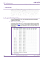
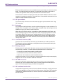
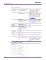
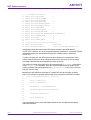
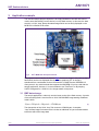
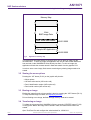
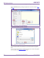
AN11071 In-Application Programming for the LPC1700 Rev. 1 — 1 May 2011 Application note Document information Info Content Keywords In-Application Programming, IAP, Flash Programming, LPC1700, Data Storage, BMP Abstract This application note briefly demonstrates on how to use the LPC1700’s In-Application Programming routines to store data in the on-chip’s flash memory. AN11071 NXP Semiconductors In-Application Programming for the LPC1700 Revision history Rev Date Description 1 Initial version. 20110501 Contact information For more information, please visit: http://www.nxp.com For sales office addresses, please send an email to: [email protected] AN11071 Application note All information provided in this document is subject to legal disclaimers. Rev. 1 — 1 May 2011 © NXP B.V. 2011. All rights reserved. 2 of 12 AN11071 NXP Semiconductors In-Application Programming for the LPC1700 1. Introduction In-Application (IAP) programming performs erase and write operations on the on-chip flash memory as directed by the user application code. IAP routines are located on the LPC1700’s boot read only memory (Boot ROM) where it can be easily executed without much overhead. A user application that can erase and write to the on-chip flash, can utilize the flash memory for data storage and in-field application programming updates. The objective of this application note is simply to provide a sample project on how to use the LPC1700’s IAP routines. Full details on how to use the IAP routines are found in the LPC1700 user manual in the “Flash memory interface and programming” section. 2. In-Application Programming This section briefly describes some of the details associated with the In-Application Programming (IAP) routines. 2.1 Flash memory and sector layout On-chip flash memory on the LPC1700 family is grouped into different number of flash sector arrangements (Fig 1). The amount of flash available to the user is dependent on the particular LPC1700 device. The largest device in the LPC1700 family contains up to 512 kB of flash. (1) Sector table taken from the LPC17xx user manual Fig 1. AN11071 Application note Sector numbers All information provided in this document is subject to legal disclaimers. Rev. 1 — 1 May 2011 © NXP B.V. 2011. All rights reserved. 3 of 12 AN11071 NXP Semiconductors In-Application Programming for the LPC1700 Erase and write operations to the on-chip flash memory are always on a sector-by-sector basis. This means that when any portion of a particular sector needs to be erased or modified, the operation needs to be performed onto the entire flash sector. Source data to be written into flash must always be located in RAM in order for the write operation to complete successfully. This means that it is not possible write data from one location in flash to another location in flash. 2.2 IAP precautions This section briefly discusses some items that may require special attention when using IAP commands. 2.2.1 Interrupts Any accesses to the flash memory must be avoided during write or erase operations. For example, if the Cortex-M3’s vector interrupt table is located in flash, all interrupts must be disabled prior to an IAP write or erase routine call. When using LPC175x/6x devices, it is possible to allow interrupts during IAP write and erase operations only if both the interrupt vector table and the interrupt service routines are located in RAM. This feature is not available with the LPC177x/8x devices as the vector interrupt table is automatically re-mapped to the interrupt vector table located in the on-chip ROM during IAP calls; effectively circumventing any flash or RAM based interrupt vector table. 2.2.2 Code Read Protection (CRP) Unlike the ISP commands, IAP commands are not affected by the CRP mechanisms. This allows the end-user application to modify flash memory contents while having the part’s security features enabled. 2.2.3 Flashing sector 0 Flashing sector 0 is performed in the same manner as every other flash sector on the microcontroller. However, it is worth mentioning that flash sector 0 includes the: Cortex-M3’s vectored interrupt table (Located at 0x0) Code Read Protection (Located at address 0x2FC) Valid user code checksum (Located at address 0x1C) If writing to this sector, it is up to the user to ensure that those three regions are properly assigned. See the user manual for additional information. 2.2.4 IAP RAM resources IAP function calls utilize 32 bytes of space in the top portion of the on-chip RAM for execution and up to 128 bytes of stack space. The user program should not use this space if IAP flash programming is permitted in the application. 2.3 IAP routines function list In-Application Programming consists of several different commands, including those that allow a user application to erase and write to flash memory. A brief list of IAP commands is listed below. Detailed instructions on how to use the IAP commands can be found in the user manual. AN11071 Application note All information provided in this document is subject to legal disclaimers. Rev. 1 — 1 May 2011 © NXP B.V. 2011. All rights reserved. 4 of 12 AN11071 NXP Semiconductors In-Application Programming for the LPC1700 Table 1. IAP commands IAP Command Functional description Precautions Prepare sector(s) for Turns off the write protection for write operation the specified flash sectors. This function must be called prior to executing “Copy RAM to Flash” or “Erase Sector(s)” commands. Copy RAM to Flash A flash sector must be prepared for write operation before contents can be written. Performs a write operation from RAM to flash memory. Ensure no other flash accesses are performed during the copy procedure. Source data must be located in RAM. See IAP precautions Erase Sector(s) Erases the contents of the entire flash sector(s). A flash sector must be prepared for write operation before it can be erased. Erased flash sector(s) will read back with all bits set to 1’s. Ensure no other flash accesses are performed during the erase procedure. See IAP precautions Blank check sector(s) Determines if flash sector(s) is(are) erased. None Read part Returns the identification number None identification number of a particular part. See the user manual for the specific part identification numbers. Read boot code version number Returns the boot ROM version number. None Read device serial number Returns the part’s unique serial number. None Compare (memory) Compares memory contents at two locations. None Re-invoke ISP This function call will invoke the ISP routine located on the boot ROM. Calling this function will remap the boot vectors, enable UART0 and Timer1 and change their PCLK values to CCLK/4. See the user manual for specific details. 2.4 Executing IAP commands IAP functions are executed out of the on-chip ROM and can be defined in the following manner: 1 2 3 4 5 6 7 8 9 10 11 AN11071 Application note /* IAP Command Definitions */ #define IAP_CMD_PREPARE_SECTORS #define IAP_CMD_COPY_RAM_TO_FLASH #define IAP_CMD_ERASE_SECTORS #define IAP_CMD_BLANK_CHECK_SECTORS #define IAP_CMD_READ_PART_ID #define IAP_CMD_READ_BOOT_ROM_VERSION #define IAP_CMD_COMPARE #define IAP_CMD_REINVOKE_ISP #define IAP_CMD_READ_SERIAL_NUMBER 50 51 52 53 54 55 56 57 58 All information provided in this document is subject to legal disclaimers. Rev. 1 — 1 May 2011 © NXP B.V. 2011. All rights reserved. 5 of 12 AN11071 NXP Semiconductors In-Application Programming for the LPC1700 12 13 14 15 16 17 18 19 20 21 22 23 24 25 26 27 28 29 /* IAP Command Status Codes */ #define IAP_STA_CMD_SUCCESS 0 #define IAP_STA_INVALID_COMMAND 1 #define IAP_STA_SRC_ADDR_ERROR 2 #define IAP_STA_DST_ADDR_ERROR 3 #define IAP_STA_SRC_ADDR_NOT_MAPPED 4 #define IAP_STA_DST_ADDR_NOT_MAPPED 5 #define IAP_STA_COUNT_ERROR 6 #define IAP_STA_INVALID_SECTOR 7 #define IAP_STA_SECTOR_NOT_BLANK 8 #define IAP_STA_SECTOR_NOT_PREPARED_FOR_WRITE_OPERATION 9 #define IAP_STA_COMPARE_ERROR 10 #define IAP_STA_BUSY 11 #define IAP_STA_INVALD_PARAM 12 /* IAP boot ROM location and access function */ #define IAP_ROM_LOCATION 0x1FFF1FF1UL #define IAP_EXECUTE_CMD(a, b) ((void (*)())(IAP_ROM_LOCATION))(a, b) Note that the physical location of the IAP routines resides in the ROM address 0x1FFF1FF0. However, due to the Cortex-M instruction architecture, executable Thumb2 instructions needs to be odd and therefore the IAP’s ROM location is defined as 0x1FFF1FF1. To make a function call, the IAP requires two array pointers for its arguments. Each pointer needs to point to a 32-bit unsigned integer array. One array is used to supply command codes and the other facilitates the return of results. The maximum number for arguments in the command array (au32Command[]) and results array (au32Result[]) is 5 elements. Once the command array has been filled with the proper command code and arguments the IAP_EXECUTE_CME(a,b) macro can be used for easy IAP function calls. Based on the IAP definitions used above, a simple IAP call can be made as shown below. This function is a wrapper function that returns the part’s identification number. 30 uint32_t u32IAP_ReadPartID(uint32_t *pu32PartID) { 31 uint32_t au32Result[5]; 32 uint32_t au32Command[5]; 33 34 au32Command[0] = IAP_CMD_READ_PART_ID; 35 36 IAP_EXECUTE_CMD(au32Command, au32Result); 37 38 *pu32PartID = au32Result[1]; 39 40 return au32Result[0]; 41 42 } The complete IAP source code and header definitions are included with the sample application software. AN11071 Application note All information provided in this document is subject to legal disclaimers. Rev. 1 — 1 May 2011 © NXP B.V. 2011. All rights reserved. 6 of 12 AN11071 NXP Semiconductors In-Application Programming for the LPC1700 3. Application example The included sample project’s objective is to simply illustrate on how IAP calls can be used to store data directly into the device’s on-chip flash memory. In this case, the data stored is a 16-bit “.bmp” bitmap formatted image which can be easily displayed on the MCB1700’s 320x240 LCD screen. Fig 2. Keil’s MCB1700 development board The project’s human interface is shown in Fig 2. It stores an image in the part’s on-chip flash which can then be displayed directly onto the graphics LCD. An image is transferred from a workstation to the microcontroller via UART0 and a XMODEM-1K client protocol. Any serial terminal that supports the XMODEM-1K can be used with the sample application; however, it is recommended to use TeraTerm Pro. By keeping UART0 configured for 115200-N-1, the image transfer is kept short. 3.1 BMP data storage The sample application’s code only uses the lower portion of the flash memory. A portion of the remaining flash is used to store a 16-bit 320x240 BMP image starting at address 0x0001 0000. 2bytes 320 pixels 240 pixels 153600bytes (1) The data portion of the 16-bit “.bmp” file consumes 153600 bytes. A complete “.bmp” bitmap image file however also includes an additional 14 byte meta-data header before the start of the image data. AN11071 Application note All information provided in this document is subject to legal disclaimers. Rev. 1 — 1 May 2011 © NXP B.V. 2011. All rights reserved. 7 of 12 AN11071 NXP Semiconductors In-Application Programming for the LPC1700 Memory Map 16-bit BMP Image Data BMP meta-data header 0x0001 0000 Sample IAP Application 0x0000 0000 Fig 3. Application memory map This application uses flash sectors 16 through 20 to view or store an image into the microcontroller. To store an image, the application will use IAP calls to flash data that it has received via the XMODEM-1K client directly into flash. To view an image, the application will take the contents stored in flash and transfer it to the graphics LCD. In order to store a new image, flash sectors containing any existing image needs to be erased. 3.2 Viewing the menu options Pressing the “UP” button (P1.23) on the joystick will print the: Menu options IAP boot code version (IAP routine call) Part’s identification number (IAP routine call) Part’s serial number (IAP routine call) 3.3 Erasing an image Erasing the image from the microcontroller is done by pressing the “INT0” button (P2.10). To verify that the image is erased, see Displaying an image. Prior to flashing a new image, the flash storage memory needs to be erased. 3.4 Transferring an image To initiate the microcontroller’s XMODEM-1K client, press the “CENTER” button (P1.20) on the joystick. Before the image can be stored in flash, the flash sectors need to be erased. Open TeraTerm Pro and configure the serial terminal for 115200-N-1. AN11071 Application note All information provided in this document is subject to legal disclaimers. Rev. 1 — 1 May 2011 © NXP B.V. 2011. All rights reserved. 8 of 12 AN11071 NXP Semiconductors In-Application Programming for the LPC1700 Start the XMODEM transfer by sending a formatted 16-bit “.bmp” file as shown in Fig 4 and Fig 5. Fig 4. TeraTerm Pro – Selecting XMODEM Send… Ensure that the XMODEM-1K protocol is selected. Fig 5. TeraTerm Pro – Selecting 1K mode For convenience, the application note software bundle includes a few sample images that are already formatted (16-bit 320x240) to be used with the MCB1700’s graphics LCD. Once the image transfer has been completed, the image can be viewed on the graphics LCD. To do this, see the Displaying an image section. AN11071 Application note All information provided in this document is subject to legal disclaimers. Rev. 1 — 1 May 2011 © NXP B.V. 2011. All rights reserved. 9 of 12 AN11071 NXP Semiconductors In-Application Programming for the LPC1700 3.5 Displaying an image A stored image that is flashed in the microcontroller is displayed onto the graphics LCD when the “DOWN” button (P1.25) on the joystick is pressed. If no image is stored on the microcontroller, the entire graphics LCD will display a white screen (because flash contains all 0xFFFF). 4. Conclusion The IAP routines available on the LPC1700 provide an easy and simply way to store data for data storage or for program code into flash memory. As these routines are stored on the part’s on-chip ROM, the user application does not require much overhead to utilize the entire chip’s flash memory. For additional details on how the IAP routines operation, see the LPC1700 user manual. AN11071 Application note All information provided in this document is subject to legal disclaimers. Rev. 1 — 1 May 2011 © NXP B.V. 2011. All rights reserved. 10 of 12 AN11071 NXP Semiconductors In-Application Programming for the LPC1700 5. Legal information application and use of customer’s third party customer(s). Customers should provide appropriate design and operating safeguards to minimize the risks associated with their applications and products. 5.1 Definitions Draft — The document is a draft version only. The content is still under internal review and subject to formal approval, which may result in modifications or additions. NXP Semiconductors does not give any representations or warranties as to the accuracy or completeness of information included herein and shall have no liability for the consequences of use of such information. 5.2 Disclaimers Limited warranty and liability — Information in this document is believed to be accurate and reliable. However, NXP Semiconductors does not give any representations or warranties, expressed or implied, as to the accuracy or completeness of such information and shall have no liability for the consequences of use of such information. In no event shall NXP Semiconductors be liable for any indirect, incidental, punitive, special or consequential damages (including - without limitation lost profits, lost savings, business interruption, costs related to the removal or replacement of any products or rework charges) whether or not such damages are based on tort (including negligence), warranty, breach of contract or any other legal theory. Notwithstanding any damages that customer might incur for any reason whatsoever, NXP Semiconductors’ aggregate and cumulative liability towards customer for the products described herein shall be limited in accordance with the Terms and conditions of commercial sale of NXP Semiconductors. Right to make changes — NXP Semiconductors reserves the right to make changes to information published in this document, including without limitation specifications and product descriptions, at any time and without notice. This document supersedes and replaces all information supplied prior to the publication hereof. Suitability for use — NXP Semiconductors products are not designed, authorized or warranted to be suitable for use in life support, life-critical or safety-critical systems or equipment, nor in applications where failure or malfunction of an NXP Semiconductors product can reasonably be expected to result in personal injury, death or severe property or environmental damage. NXP Semiconductors accepts no liability for inclusion and/or use of NXP Semiconductors products in such equipment or applications and therefore such inclusion and/or use is at the customer’s own risk. Applications — Applications that are described herein for any of these products are for illustrative purposes only. NXP Semiconductors makes no representation or warranty that such applications will be suitable for the specified use without further testing or modification. NXP Semiconductors does not accept any liability related to any default, damage, costs or problem which is based on any weakness or default in the customer’s applications or products, or the application or use by customer’s third party customer(s). Customer is responsible for doing all necessary testing for the customer’s applications and products using NXP Semiconductors products in order to avoid a default of the applications and the products or of the application or use by customer’s third party customer(s). NXP does not accept any liability in this respect. Export control — This document as well as the item(s) described herein may be subject to export control regulations. Export might require a prior authorization from national authorities. Evaluation products — This product is provided on an “as is” and “with all faults” basis for evaluation purposes only. NXP Semiconductors, its affiliates and their suppliers expressly disclaim all warranties, whether express, implied or statutory, including but not limited to the implied warranties of noninfringement, merchantability and fitness for a particular purpose. The entire risk as to the quality, or arising out of the use or performance, of this product remains with customer. In no event shall NXP Semiconductors, its affiliates or their suppliers be liable to customer for any special, indirect, consequential, punitive or incidental damages (including without limitation damages for loss of business, business interruption, loss of use, loss of data or information, and the like) arising out the use of or inability to use the product, whether or not based on tort (including negligence), strict liability, breach of contract, breach of warranty or any other theory, even if advised of the possibility of such damages. Notwithstanding any damages that customer might incur for any reason whatsoever (including without limitation, all damages referenced above and all direct or general damages), the entire liability of NXP Semiconductors, its affiliates and their suppliers and customer’s exclusive remedy for all of the foregoing shall be limited to actual damages incurred by customer based on reasonable reliance up to the greater of the amount actually paid by customer for the product or five dollars (US$5.00). The foregoing limitations, exclusions and disclaimers shall apply to the maximum extent permitted by applicable law, even if any remedy fails of its essential purpose. 5.3 Trademarks Notice: All referenced brands, product names, service names and trademarks are property of their respective owners. Customers are responsible for the design and operation of their applications and products using NXP Semiconductors products, and NXP Semiconductors accepts no liability for any assistance with applications or customer product design. It is customer’s sole responsibility to determine whether the NXP Semiconductors product is suitable and fit for the customer’s applications and products planned, as well as for the planned AN11071 Application note All information provided in this document is subject to legal disclaimers. Rev. 1 — 1 May 2011 © NXP B.V. 2011. All rights reserved. 11 of 12 AN11071 NXP Semiconductors In-Application Programming for the LPC1700 6. Contents 1. 2. 2.1 2.2 2.2.1 2.2.2 2.2.3 2.2.4 2.3 2.4 3. 3.1 3.2 3.3 3.4 3.5 4. 5. 5.1 5.2 5.3 6. Introduction .........................................................3 In-Application Programming ..............................3 Flash memory and sector layout ........................3 IAP precautions..................................................4 Interrupts ............................................................4 Code Read Protection (CRP) .............................4 Flashing sector 0................................................4 IAP RAM resources............................................4 IAP routines function list.....................................4 Executing IAP commands ..................................5 Application example ...........................................7 BMP data storage ..............................................7 Viewing the menu options ..................................8 Erasing an image ...............................................8 Transferring an image ........................................8 Displaying an image .........................................10 Conclusion.........................................................10 Legal information ..............................................11 Definitions ........................................................11 Disclaimers.......................................................11 Trademarks ......................................................11 Contents.............................................................12 Please be aware that important notices concerning this document and the product(s) described herein, have been included in the section 'Legal information'. © NXP B.V. 2011. All rights reserved. For more information, please visit: http://www.nxp.com For sales office addresses, please send an email to: [email protected] Date of release: 1 May 2011 Document identifier: AN11071