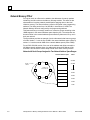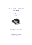
1
GE
Intelligent Platforms
Programmable Control Products
PACSystems*
Memory Xchange Modules
User’s Manual, GFK-2300D
March 2010
GFL-002
Warnings, Cautions, and Notes
as Used in this Publication
Warning
Warning notices are used in this publication to emphasize that hazardous voltages,
currents, temperatures, or other conditions that could cause personal injury exist in this
equipment or may be associated with its use.
In situations where inattention could cause either personal injury or damage to equipment,
a Warning notice is used.
Caution
Caution notices are used where equipment might be damaged if care is not taken.
Note:
Notes merely call attention to information that is especially significant to
understanding and operating the equipment.
This document is based on information available at the time of its publication. While efforts
have been made to be accurate, the information contained herein does not purport to cover all
details or variations in hardware or software, nor to provide for every possible contingency in
connection with installation, operation, or maintenance. Features may be described herein
which are not present in all hardware and software systems. GE Intelligent Platforms assumes
no obligation of notice to holders of this document with respect to changes subsequently made.
GE Intelligent Platforms makes no representation or warranty, expressed, implied, or statutory
with respect to, and assumes no responsibility for the accuracy, completeness, sufficiency, or
usefulness of the information contained herein. No warranties of merchantability or fitness for
purpose shall apply.
* indicates a trademark of GE Intelligent Platforms, Inc. and/or its affiliates. All other
trademarks are the property of their respective owners.
©Copyright 2010 GE Intelligent Platforms, Inc.
All Rights Reserved
Contact Information
If you purchased this product through an Authorized Channel Partner, please contact the seller
directly.
General Contact Information
Online technical support and
GlobalCare
http://www.ge-ip.com/support
1H2
Additional information
http://www.ge-ip.com/
3H
Solution Provider
[email protected]
4H
Technical Support
If you have technical problems that cannot be resolved with the information in this guide, please
contact us by telephone or email, or on the web at www.ge-ip.com/support
5H
Americas
Online Technical Support
www.ge-ip.com/support
6H7
Phone
1-800-433-2682
International Americas Direct Dial
1-780-420-2010 (if toll free 800 option is unavailable)
Technical Support Email
[email protected]
8H9
Customer Care Email
Primary language of support
[email protected]
10H
English
Europe, the Middle East, and Africa
Online Technical Support
www.ge-ip.com/support
12H3
Phone
+800-1-433-2682
EMEA Direct Dial
+352-26-722-780 (if toll free 800 option is unavailable or if
dialing from a mobile telephone)
Technical Support Email
[email protected]
14H5
Customer Care Email
Primary languages of support
[email protected]
16H7
English, French, German, Italian, Czech, Spanish
Asia Pacific
Online Technical Support
www.ge-ip.com/support
Phone
18H9
+86-400-820-8208
+86-21-3217-4826 (India, Indonesia, and Pakistan)
Technical Support Email
[email protected] (China)
20H1
[email protected] (Japan)
2H3
[email protected] (remaining Asia customers)
24H5
Customer Care Email
[email protected]
26H7
[email protected] (China)
28H
Contents
Introduction....................................................................................................................1-1
Overview ........................................................................................................................... 1-2
Basic Memory Xchange Operation .......................................................................... 1-2
Sample Memory Xchange Network ......................................................................... 1-3
Memory Xchange Features .............................................................................................. 1-4
RX3i Reflective Memory Module Features .............................................................. 1-4
IC695CMX128 and IC695RMX128 Functional Compatibility .................................. 1-5
RX7i Reflective Memory Module Features .............................................................. 1-6
IC698CMX016 and IC698RMX016 Functional Compatibility .................................. 1-7
Reflective Memory Hub............................................................................................ 1-7
QuickStart ......................................................................................................................2-1
Installation and Configuration......................................................................................3-1
RX3i Memory Xchange Module User Features ................................................................ 3-2
CMX128 LEDs ......................................................................................................... 3-2
RMX128 LEDs ......................................................................................................... 3-3
Optical Transceiver .................................................................................................. 3-3
RX7i Memory Xchange Module User Features ................................................................ 3-4
Role Switch (RMX Only) .......................................................................................... 3-5
Node ID .................................................................................................................... 3-5
Redundant Transfer Mode Operation ...................................................................... 3-5
Network Memory Offset ........................................................................................... 3-6
Rogue Packet Detection and Removal .................................................................... 3-7
Physical Installation .......................................................................................................... 3-8
RX3i Memory Xchange Modules ............................................................................. 3-8
RX7i Memory Xchange Modules ............................................................................. 3-9
Network Connection........................................................................................................ 3-10
VMICBL-000-F5-0xx Cable Lengths ...................................................................... 3-10
Fiber-optic Connectors........................................................................................... 3-10
Fiber-optic Cables .................................................................................................. 3-11
Hardware Configuration.................................................................................................. 3-12
Configuring a Memory Xchange Module................................................................ 3-12
Configuration Parameters ...................................................................................... 3-13
Basic Operation .............................................................................................................4-1
Powerup and Initialization................................................................................................. 4-1
BUS_ Functions ................................................................................................................ 4-2
Multiple Writes to Network Memory .................................................................................. 4-4
Data Transfer Time ........................................................................................................... 4-5
RX3i Read/Write Transfer Times ............................................................................. 4-5
RX7i Read/Write Transfer Times ............................................................................. 4-5
Estimating Total Transfer Time ................................................................................ 4-6
Special Considerations for Stores of Configuration.......................................................... 4-7
GFK-2300D
v
Contents
Advanced Operation .....................................................................................................5-1
Module Interrupts .............................................................................................................. 5-2
Interrupt Initialization Logic ...................................................................................... 5-4
Interrupt Handling Logic ........................................................................................... 5-5
Associating Module Interrupts with Logic................................................................. 5-6
Dynamic Masking of Module Interrupts.................................................................... 5-6
Network Interrupts............................................................................................................. 5-8
Sending Network Interrupts...................................................................................... 5-8
Receiving Network Interrupts ................................................................................... 5-8
Memory Parity Checking................................................................................................. 5-11
On-demand Memory Clear ............................................................................................. 5-13
Checking Ring Integrity................................................................................................... 5-13
Optimizing Network Bandwidth....................................................................................... 5-14
Using Network Interrupts to Balance Network Load .............................................. 5-14
Memory Xchange Module Specifications................................................................... A-1
Register Definitions...................................................................................................... B-1
Region 2: Primary Control and Status Registers.............................................................. B-2
Local Control and Status Register (LCSR) .............................................................. B-3
Local Interrupt Status Register (LISR) ..................................................................... B-5
Local Interrupts Enable Register (LIER) .................................................................. B-7
Registers for Generating Network Interrupts ........................................................... B-8
Registers for Receiving Network Interrupts ............................................................. B-9
Region3: Auxiliary Control and Status Registers............................................................ B-11
Offset 440h............................................................................................................. B-11
Offset 441h............................................................................................................. B-11
Offset 442h............................................................................................................. B-12
Offset 445h............................................................................................................. B-12
Offset 446h............................................................................................................. B-12
Region 4: Interrupt Acknowledge Register ..................................................................... B-13
Interrupt Acknowledge Register (IAKR) ................................................................. B-13
vi
PACSystems™ Memory Xchange Modules User’s Manual–March 2009
GFK-2300D
Chapter
Introduction
1
This manual describes the features, installation, and operation of the following
Memory Xchange modules in a PACSystems reflective memory network:
IC695CMX128
IC695RMX128
IC698CMX016
IC698RMX016
RX3i Control Memory Xchange (CMX) module
RX3i Redundancy Memory Xchange (RMX) module
RX7i Control Memory Xchange (CMX) module
RX7i Redundancy Memory Xchange (RMX) module
This chapter presents an overview of Memory Xchange operation (page 1-2), and a
summary of Memory Xchange features and functional compatibility (page 1-4).
For additional information, refer to the following chapters:
■
Chapter 2, “QuickStart” – Provides an overview of the steps needed to configure
and operate a reflective memory network and to verify Memory Xchange
operation.
■
Chapter 3, “Installation and Configuration” – describes user features, and provides
procedures for physical installation and software configuration.
■
Chapter 4, “Basic Operation” – describes the operation of basic Memory Xchange
module functions and how to access them.
■
Chapter 5, “Advanced Operation” – describes how to use the advanced
capabilities of the Memory Xchange module
■
Appendix A, “Memory Xchange Module Specifications” – provides performance
and environmental specifications.
■
Appendix B, “Register Definitions” – provides detailed definitions of the module’s
registers.
Related Publications
PACSystems CPU Reference Manual, GFK-2222
PACSystems RX7i Installation Manual, GFK-2223
PACSystems RX3i System Manual, GFK-2314
PACSystems RX7i User's Guide to Integration of VME Modules, GFK-2235
PACSystems Hot Standby CPU Redundancy User’s Manual, GFK-2308
Proficy Machine Edition Logic Developer Getting Started, GFK-1918
For the most recent versions of PACSystems and related documentation, visit the GE
website: http://www.ge-ip.com/
GFK-2300D
1-1
1
Overview
The Memory Xchange modules use reflective memory technology, which allows the
deterministic sharing of data among Controllers and other computing devices on a
high-speed fiber optic network. Deterministic networks enable sharing of data within a
predetermined time interval. The network can be made up of any combination of these
modules and other reflective memory devices that are network compatible with the
GE Embedded Systems 5565 family. Each such device is a node on the
network. A reflective memory network can contain up to 256 nodes. Whenever data is
written to one node, all nodes on the network are automatically updated with the new
data.
Each node in the reflective memory network is connected in a daisy-chained loop
using fiber-optic cables. The transmitter of the first node is tied to the receiver of the
second. The transmitter of the second node is tied to the receiver of the third node,
and so on, until the loop is completed back at the receiver of the first node. The figure
on page 1-5 shows an example of a seven-node reflective memory network.
The RMX modules can be used in a redundant system (two CPUs), as part of a
redundancy link. A complete redundancy link consists of one RMX in the primary unit,
one RMX in the secondary unit, and high-speed fiber optic cables connecting them to
each other. This must be a two-node ring: no other reflective memory nodes are
allowed to be part of this fiber optic network. When the RMX is being used as
redundancy link, it cannot be used as a general-purpose Memory Xchange module.
When the RMX is not being used as a redundancy link, it is functionally identical to the
CMX module.
For details on the operation of a PACSystems Hot Standby CPU redundancy system,
refer to the PACSystems Hot Standby CPU Redundancy User’s Manual, GFK-2308.
Basic Memory Xchange Operation
After the module has been configured, a transfer of data over the network can be
initiated by writing to the reflective memory region through the backplane bus. The
Memory Xchange module forms the data into variable length packets sized from 4 to
64 bytes, which it transmits over the fiber-optic network to the receiver of the next
node. Whenever a packet is received, the Memory Xchange module evaluates the
packet. If the packet is valid and did not originate on this node, it is accepted. If,
however, the data packet is invalid or if it originated at this node, it is discarded. The
receiving node writes the data into the local reflective memory and simultaneously
transmits the data to the next node on the network. From there, the process is
repeated until the data returns to the originating node, where it is removed from the
network.
Basic operating functions are configured using Proficy™ Machine Edition Logic
Developer.
1-2
PACSystems™ Memory Xchange Modules User’s Manual – March 2009
GFK-2300D
1
Sample Memory Xchange Network
CMX
PCI WorkStation with
VMIPCI-5565 reflective
memory board
CMX
CMX
CMX
GFK-2300D
Chapter 1 Introduction
1-3
1
Memory Xchange Features
RX3i Reflective Memory Module Features
A PACSystems RX3i main rack supports a maximum of six Memory Xchange
modules.
1-4
■
PACSystems RX3i single slot form factor.
■
128 Mbytes reflective memory with parity.
■
Software configuration of all node parameters (no
jumper or switch settings required).
■
No RX3i CPU processing required to operate the
network.
■
Network-compatible with the GE
Embedded Systems 5565 family of reflective
memory devices.
■
Connection with multimode fiber up to 1000 ft. or
304.80m.
■
Dynamic packet sizes of 4 to 64 bytes, controlled
by the CMX module.
■
Network transfer rate of 43 Mbyte/s (4 byte
packets) to 174 Mbyte/s (64 byte packets)
■
Network link speed of 2.1 Gbits/s
■
Programmable module interrupt.
■
Four general-purpose network interrupts with 32
bits of data each.
■
Network error detection.
■
Up to 256 nodes per network.
OK
OK
CONFIG
LINK OK
SIG DETECT
SIG DETECT
OWN DATA
OWN DATA
CMX128
RMX128
NODE
1
ROLE
SWITCH
0
LOCAL
READY
ACTIVE
REMOTE
■
Redundant transfer mode operation. This optional
mode reduces the chance of a data packet being
dropped from the network.
■
Configurable network memory offset for
compatibility with RX7i Memory Xchange
applications.
READY
ACTIVE
NODE
TX (FRONT)
TX (FRONT)
RX (BACK)
RX (BACK)
PACSystems™ Memory Xchange Modules User’s Manual – March 2009
GFK-2300D
1
IC695CMX128 and IC695RMX128 Functional Compatibility
GFK-2300D
■
PACSystems RX3i CPU with firmware version 5.50 or later for CMX128 and
PACSystems RX3i CPU with firmware version 5.70 or later for RMX128.
■
Programming software: Proficy Machine Edition Logic Developer, version 5.8
or later for CMX128 and Proficy Machine Edition Logic Developer, version 5.9
SIM1 or later for RMX128.
■
Only the RMX can operate as a redundancy link. Redundancy link operation
requires a CPU that supports CPU redundancy, such as the IC695CRU320
(firmware version 5.70 or later) and Proficy Machine Edition Logic Developer
version 5.90 SIM1 or later.
■
Compatible with reflective memory devices in the GE Embedded Systems
5565 family. The PACSystems Memory Xchange module does not operate with
other reflective memory families offered by GE Embedded Systems.
Chapter 1 Introduction
1-5
1
RX7i Reflective Memory Module Features
An RX7i main rack supports a maximum of four Memory
Xchange modules in any combination of RMX and CMX
modules. When using CPU redundancy, up to two RMX
modules in a rack can be configured as redundancy links.
CMX016
■
PACSystems single slot form factor.
■
16 Mbytes reflective memory with parity.
■
Software configuration of all node parameters (no
jumper or switch settings required).
■
No PACS CPU processing required to operate the
network.
■
Network-compatible with the GE Embedded
Systems 5565 family of reflective memory devices.
■
Connection with multimode fiber up to 1000 ft.
(304.80m).
■
Dynamic packet sizes of 4 to 64 bytes, controlled by
the Memory Xchange module.
RMX016
OK
OK
LINK OK
CONFIG
LOCAL
1-6
READY
ACTIVE
REMOTE
READY
ACTIVE
ROLE
SWITCH
1
0
■
Network transfer rate of 43 Mbyte/s (4 byte packets) to
174 Mbyte/s (64 byte packets)
■
Network link speed of 2.1 Gbits/s
■
Programmable VMEbus interrupt output.
■
Four general-purpose network interrupts with 32 bits
of data each.
■
Network error detection.
OWN DATA
OWN DATA
■
Up to 256 nodes per network.
SIGNAL DETECT
SIGNAL DETECT
■
Redundant transfer mode operation. This optional
mode reduces the chance of a data packet being
dropped from the network.
TX
TX
RX
RX
■
Configurable network memory offset allows you to
assign nodes on a network to groups according to the
16MB segment in the network address space that they
use.
IC698CMX016
IC698RMX016
PACSystems™ Memory Xchange Modules User’s Manual – March 2009
GFK-2300D
1
IC698CMX016 and IC698RMX016 Functional Compatibility
■
PACSystems RX7i CPU with firmware version 2.0 or later.
■
Only an RMX can operate as a redundancy link. To operation as a redundancy
link, RMX modules require a CPU that supports CPU redundancy, such as the
IC698CRE020.
■
Programming software: Proficy Machine Edition Logic Developer, version 4.5 or
later
■
When used as a general-purpose reflective memory module, the RX7i Memory
Xchange modules are compatible with reflective memory devices in the GE
Embedded Systems 5565 family. The PACSystems Memory Xchange module
does not operate with other reflective memory families offered by GE
Embedded Systems.
Reflective Memory Hub
The VMIACC-5595 is a managed hub designed to operate with the GE 5565
family of Reflective Memory real-time network products. The Reflective Memory hub
can automatically bypass ports when it detects a loss of signal or the loss of valid
synchronization patterns, allowing the other nodes in the network to remain
operational.
For additional information, refer to the VMIACC-5595 2Gb/s Reflective Memory Hub
Installation Guide, 522-805595-000, which is available at
http://www.ge-ip.com/support.
GFK-2300D
Chapter 1 Introduction
1-7
Chapter QuickStart
2
This chapter provides an overview of the steps needed to configure and operate a basic
reflective memory network and to verify Memory Xchange operation.
Note:
For operation of an RMX in a redundancy system, refer to the PACSystems Hot
Standby CPU Redundancy User’s Manual, GFK-2308.
Performance Recommendations
To transfer data most efficiently, use the minimum number of reads/writes possible. For
example, use one long read/write instead of several. Length is specified in data size
(DWORDS).
For maximum performance, Offset, which is specified in BYTES, should be specified in
numbers divisible by 4, so that bus accesses are DWORD aligned.
1. Install the Memory Xchange module in the rack system. If necessary, apply power to
the controller.
When power is applied to the module an internal loopback test occurs; the OWN DATA
and SIGNAL DETECT indicators turn on briefly during this test. When the Memory
Xchange module and the CPU are powered up and functioning properly, the module’s
OK indicator is on.
Warning
RX7i modules do not support hot installation and removal. Do not
insert or remove RX7i modules with power applied. This could cause
the CPU to stop, damage the module, or result in personal injury.
Note:
RX3i Memory Xchange modules support hot insertion and removal.
For installation details, refer to “Physical Installation” in chapter 3.
2. Using the Logic Developer software, add the Memory
Xchange module to the rack configuration.
GFK-2300D
2-1
2
3. Connect the module to the network.
Using an LC- compatible multimode fiber optic cable, connect the module’s TX connector
to the RX connector of the next module in the ring. Connect the fiber optic cable from that
module’s TX to the RX connector of the next module. Repeat this step until the last node
in the ring routes its TX to the RX of the first node. For cable details, see “Network
Connection” in Chapter 3.
When the fiber optic transceiver detects a signal on the network, the SIGNAL DETECT
indicator will be on.
TX
TX
TX
RX
RX
RX
4. Configure the module’s operating parameters and download the configuration to
the controller.
Each Memory Xchange module on the network must have a unique Node ID. If the
network contains more than one Memory Xchange module, change the Node ID. For
details on configuring other parameters, see “Hardware Configuration” in chapter 3.
When the module receives a configuration, it sends a test packet to determine whether all
nodes on the ring are connected with transmitters enabled. If all nodes are configured
correctly and powered on, the OWN DATA indicator should be on, indicating the module
has received its own data packet from the network at least once.
When the module is configured, its CONFIG or LINK OK indicator is on.
2-2
PACSystems™ Memory Xchange Modules User’s Manual – March 2009
GFK-2300D
2
5. Use a BUS_WRT_DWORD function to write data to the network.
Do not inadvertently overwrite data from another node.
To detect whether the write operation succeeded or failed, record the value of the ST
(status) output and note whether the BUS_WRT function passed power. For example, if
the module is not in the rack or if an incorrect slot number is used as an input to the
function, the BUS_WRT operation will not succeed.
If the bus write operation is successful, the BUS_WRT function will pass power and the
ST output will have a value of 0.
In the following example, the inputs R, S, RGN and OFF indicate the data is being written
to a module located in Rack 0, Slot 5, Region 1 and Offset 16.
For details on the use of BUS_WRT and BUS_RD functions, refer to “BUS_ Functions” in
Chapter 4.
BUS_WRT_DWORD Function Details
Parameter
??
Definition
Length. Specifies the number of DWORDs to write.
Inputs
IN
Starting address of the data to write. Must be a DWORD variable.
R
Rack location of module. For a Memory Xchange module, must be 0 (Main rack).
S
Slot location of module.
SS
Subslot (always 0)
RGN
Region in module user memory to write to. Region 1 corresponds to the module’s
reflective memory.
OFF
BYTE offset of starting address to be written to within the memory region. This is a
0-based address. Note that Offset is specified in BYTEs regardless of the type of
BUS_ function being used.
For maximum performance, Offset should be specified in numbers divisible by 4, so
that bus access is DWORD aligned.
Output
ST
GFK-2300D
Status word for the write operation.
Chapter 2 QuickStart
2-3
2
6. Use a BUS_RD_DWORD function to read data from the network.
If the bus read operation is successful, the ST output will have a value of 0.
If the Bus_RD function passes power, the data requested is present and valid.
If the Bus_RD function does not pass power, the data may be in an indeterminate state –
for example if loss of module occurred during read. Check the ST (status) output to
determine the cause of failure.
The DWORD value returned in the output Q should be the same as the value written in
step 4.
In the following example, the inputs R, S, RGN and OFF indicate the data is being read
from a module located in Rack 0, Slot 5, Region 1 and Offset 16.
BUS_RD_DWORD Function Details
Parameter
??
Definition
Length. Specifies the number of DWORDs to read.
Inputs
R
Rack location of module. For a Memory Xchange module, must be 0 (Main rack).
S
Slot location of module.
SS
Subslot (always 0)
RGN
Region in module user memory to read from. Region 1 corresponds to the module’s
reflective memory.
OFF
BYTE offset of starting address to be read from within the memory region. This is a
0-based address. Note that Offset is specified in BYTEs regardless of the type of
BUS_ function being used.
For maximum performance, Offset should be specified in numbers divisible by 4, so
that bus access is DWORD aligned.
Outputs
2-4
ST
Status word for the read operation.
Q
Starting address where the data is to be placed. Must be a DWORD variable.
PACSystems™ Memory Xchange Modules User’s Manual – March 2009
GFK-2300D
Chapter
Installation and Configuration
3
This chapter provides a guide to the user features, physical installation, and initial
configuration of the Memory Xchange module.
Before you can use the Memory Xchange module, you must configure it using
Proficy Machine Edition Logic Developer software. The programming software
allows you to specify a basic hardware configuration for the Memory Xchange
module that allows it to operate in a reflective memory network or as a
redundancy link (RMX modules only).
GFK-2300D
3-1
3
RX3i Memory Xchange Module User Features
CMX128 LEDs
LED Label
Description
OK
OK
ON indicates the module and
the CPU are functioning
properly.
CONFIG*
ON indicates the module is
configured.
SIG DETECT
ON indicates the receiver is
detecting a fiber optic signal.
OWN DATA
ON indicates the module has
received its own data packet
from the network at least once.
CONFIG
SIG DETECT
OWN DATA
CMX128
NODE
* A reflective memory hub can be used to
bypass a node that is not configured.
Optical
Transceiver
(bottom view)
TX
TX (FRONT)
RX (BACK)
RX
3-2
PACSystems™ Memory Xchange Modules User’s Manual – March 2009
GFK-2300D
3
RMX128 LEDs
LED Label
OK
LINK OK
Description
OK
ON indicates the module is
functioning properly.
LINK OK
SIG DETECT
OWN DATA
When used as a redundancy link,
ON indicates the link is
functioning properly. When not
used as a redundancy link, ON
indicates the module is
configured.
SIG DETECT
ON indicates the receiver is
detecting a fiber optic signal.
OWN DATA
ON indicates the module has
received its own data packet from
the network at least once.
LOCAL
READY
ON indicates the local unit
is ready.
LOCAL
ACTIVE
ON indicates the local unit
is active.
REMOTE
READY
ON indicates the remote unit
is ready.
REMOTE
ACTIVE
ON indicates the remote unit
is active.
RMX128
1
ROLE
SWITCH
0
LOCAL
READY
ACTIVE
REMOTE
Optical
Transceiver
(bottom view)
TX
READY
ACTIVE
NODE
TX (FRONT)
RX (BACK)
RX
Optical Transceiver
The optical transceiver, which is located on the bottom of the module, has two
“LC” type fiber optic ports. The port labeled “TX” is the transmitter and the port
labeled “RX” is the receiver.
CMX modules are networked together using either simplex (single fiber) or duplex
(dual fiber) multimode fiber optic cables. The specific cable construction depends
on your operating environment. For details on cables, see “Fiber Optic Cables and
Connectors” on page 3-10.
GFK-2300D
Chapter 3 Installation and Configuration
3-3
3
RX7i Memory Xchange Module User Features
CMX016 LEDs
The general purpose RX7i CMX module has four LEDs and an optical
transceiver.
LED Label
CMX016
RMX016
Description
OK
ON indicates the module and CPU are functioning properly.
CONFIG*
Indicates the module is configured.
OWN DATA
ON indicates the module has received its own data packet from
the network at least once.
SIGNAL DETECT
OK
OK
LINK OK
CONFIG
LOCAL
READY
ACTIVE
ON indicates the receiver is detecting a fiber optic signal.
* A reflective memory hub can be used to bypass a node that is not configured.
REMOTE
READY
ACTIVE
RMX016 LEDs
The RX7i RMX module has eight LEDs, a role switch and an optical transceiver.
LED Label
Description
OK
ON indicates the module and CPU are functioning properly.
LINK OK
When not used as a redundancy link, ON indicates the
module is configured.
When used as a redundancy link, ON indicates the link is
functioning properly.
LOCAL READY
ON indicates the local unit is ready.
ROLE
SWITCH
1
0
LOCAL ACTIVE
ON indicates the local unit is active.
REMOTE READY
ON indicates the remote unit is ready.
REMOTE ACTIVE
ON indicates the remote unit is active.
OWN DATA
ON indicates the module has received its own data packet
from the network at least once.
SIGNAL DETECT
ON indicates the receiver is detecting a fiber optic signal.
Optical Transceiver
OWN DATA
OWN DATA
SIGNAL DETECT
SIGNAL DETECT
TX
TX
RX
RX
IC698CMX016
IC698RMX016
The optical transceiver has two “LC” type fiber optic ports. The port labeled “TX”
is the transmitter and the port labeled “RX” is the receiver. For details on cables,
see “Fiber Optic Cables and Connectors” on page 3-10.
3-4
PACSystems™ Memory Xchange Modules User’s Manual – March 2009
GFK-2300D
3
Role Switch (RMX Only)
The Role switch is a spring-loaded two-position switch that rests in the OFF state.
When the RMX module is being used as a redundancy link, this switch allows you
to manually switch control from the active controller to the backup controller. To
initiate the switching of roles, lift the switch to the ON position for at least 1
second. The role switch state is de-bounced and filtered to prevent accidental
activation.
When the RMX module is used as a node in a general-purpose reflective memory
network (i.e. not used as a redundancy link), the Role switch has no effect on
module operation.
Node ID
Each node in a reflective memory network must have a unique Node ID, which
may range from 0 through 255. Node ID is configured by the programming
software.
Redundant Transfer Mode Operation
Redundant Transfer mode is enabled or disabled using hardware configuration in
the programming software. While in the Redundant Transfer mode, each packet is
transferred on the network twice. The receiving node evaluates each redundant
transfer. If no errors are detected in the first transfer, it is used to update the onboard memory and the second transfer is discarded. If the first transfer contains
an error, the second transfer is used to update the on-board memory provided it
has no transmission error. If errors are detected in both transfers, neither transfer
is used and the data is completely removed from the network. The Bad Data bit
(Bit 01 of the LCSR in Region 2) is set if an error is detected in either transfer.
Redundant Transfer mode greatly reduces the chance that data is dropped from
the network. However, the redundant transfer mode reduces the effective network
transfer rates by approximately 50 percent.
Note:
GFK-2300D
The Redundant Transfer mode pertains only to the method of transferring
packets over the network. It does not relate to redundancy link operation
nor does it relate to the Redundancy LEDs.
Chapter 3 Installation and Configuration
3-5
3
Network Memory Offset
For a given node, an offset can be added to the addresses of network packets
initiated by local bus writes to the Memory Xchange module. This offset is also
subtracted from incoming network packets before applying them to the local
reflective memory. The network memory offset is configured in the programming
software. The offset can be from 0 to 240 MB, in increments of 16 MB. The
Network Memory Offset is configured by the programming software.
This feature allows you to assign nodes on a network to groups according to the
16MB segment in the network address space that they use. The nodes that use
the same offset in the network address space effectively behave as if they are in
their own network.
The figure below provides an example of a six-node network that has two groups
of nodes. Nodes 1—3 use the first 16 MB in the network address space (offset 0);
nodes 4—6 use the second 16MB of the network address space (offset 16MB).
For an RX3i CMX128 module, if the sum of the address and offset exceeds the
256 Mbyte network address range, the address bits beyond 256 Mbyte will be
truncated. This causes the write to wrap around into a lower memory location.
Network with Node Groups Assigned to Two Network Address Space Ranges
Network Address Space
Offset
240 MB
1
Nodes 1—3 have
offset 0
6
Nodes 4—6
have offset 16
2
224 MB
5
80 MB
64 MB
3
4
48 MB
32 MB
16 MB
0 MB
3-6
PACSystems™ Memory Xchange Modules User’s Manual – March 2009
GFK-2300D
3
Rogue Packet Detection and Removal
A rogue packet is a packet that does not seem to belong to any node on the
network. If the packet is altered as it passes through a non-originating node or if
the originating node begins to malfunction, the originating node may fail to
recognize the packet as its own and not remove the packet from the network. In
such circumstances the packet passes around the network loop indefinitely.
Rogue packets are rare. Their existence indicates a malfunctioning board due to
component failure or operation in an overly harsh environment. Normally, the
solution is to isolate and replace the malfunctioning board or improve the
environment. However, in some applications it is preferable to tolerate sporadic
rogue packets rather than halt the system for maintenance, provided the rogue
packets are removed from the network.
To prevent rogue packets from circulating on the network indefinitely, the Memory
Xchange module can be configured to operate as one of two rogue masters. A
rogue master alters each packet as it passes through its node. If that packet
returns to the rogue master a second time, the rogue master recognizes that it is a
rogue packet and removes it from the network. When a rogue packet is detected,
the rogue packet fault flag is set in the Local Interrupt Status register (LISR).
Optionally, the module may be programmed to generate a module interrupt when
this rogue packet fault is set.
The reflective memory network supports up to two rogue masters per network,
Rogue Master 0 and Rogue Master 1, so they can cross check each other.
Two boards in the same network should not be set as the same rogue master.
Otherwise, each will erroneously remove packets originated by the other.
Rogue Master operation is enabled in the programming software.
GFK-2300D
Chapter 3 Installation and Configuration
3-7
3
Physical Installation
RX3i Memory Xchange Modules
Equipment Required
■
A PACSystems RX3i CPU with release 5.50 or higher firmware
■
A PACSystems RX3i CPU rack with power supply.
■
Programming software: Machine Edition – Logic Developer, version 5.8 or
later (and a PC-compatible computer).
■
Cables. For details, see “Fiber-optic Cables and Connectors” on page 3-10.
Note:
RX3i systems that include one or more Memory Xchange modules must
be installed in a metal enclosure with conduit or equivalent to meet
radiated emission standards and maintain CE Mark compliance. For
details, refer to appendix A of the PACSystems RX3i System
Manual, GFK-2314.
Installing the Memory Xchange Module in an RX3i Rack
Memory Xchange modules must only be installed in the main (Rack 0) RX3i rack.
RX3i supports a maximum of six Memory Xchange modules per main rack.
The RX3i CMX and RMX modules support hot insertion and removal from the
RX3i baseplate.
Note:
Network disruption will occur during a hot-insertion or hot-removal
operation, even if a bypass switch is used. The network disruption can be
minimized by using an automatic bypass switch, such as that provided by
the ACC-5595 managed hub.
The redundant communication link associated with a hot swapped RMX
module will be lost. To restore the link to service, power cycle the backup
unit if the system is in operation, and if possible. If either RMX module’s
OK LED is OFF, power must be cycled on the rack to restore the RMX
module to service.
1.
Slide the module into the slot for which it was configured in the system.
2.
Press the module firmly in place, but do not force the board.
3.
Connect the fiber optic cables to the TX and RX connectors.
4.
Route the fiber optic cable connected to TX to the RX connector of the next
module in the ring. Connect the fiber optic cable from that board’s TX to the
RX connector of the next module. Repeat this step until the last node in the
ring routes its TX to the RX of the first node.
Note:
3-8
The Memory Xchange module initially powers up in an unconfigured state
with its optical transmitter disabled. The module cannot operate on a
network until the RX3i CPU has sent a hardware configuration to the
module. For additional information, see “Hardware Configuration” on
page 3-12.
PACSystems™ Memory Xchange Modules User’s Manual – March 2009
GFK-2300D
3
RX7i Memory Xchange Modules
Equipment Required
Make sure you have the items listed below before you begin.
■
A PACSystems RX7i CPU with release 2.00 or higher firmware
■
A PACSystems RX7i CPU rack with power supply.
■
Programming software: Machine Edition – Logic Developer, version 4.5 or
later (and a PC-compatible computer).
■
Cables. For details, see “Fiber-optic Cables and Connectors” on page 3-10.
Note:
RX7i systems that include one or more Memory Xchange modules must
be installed in a metal enclosure with conduit or equivalent to meet
radiated emission standards and maintain CE Mark compliance. For
details, refer to appendix A of the PACSystems RX7i Installation Manual,
GFK-2223.
Installing the Memory Xchange Module in an RX7i Rack
Warning
Do not insert or remove RX7i modules with power applied.
This could cause the CPU to stop, damage the module, or
result in personal injury.
Memory Xchange modules must only be installed in the main (Rack 0) RX7i rack.
RX7i supports a maximum of four Memory Xchange modules per main rack.
Note:
1.
Make sure rack power is off.
2.
Slide the module into the slot for which it was configured in the system.
3.
Press the board firmly in place, but do not force the board. Tighten the screws
on the top and bottom of the faceplate.
4.
Connect the fiber optic cables to the TX and RX connectors.
5.
Route the fiber optic cable connected to TX to the RX connector of the next
module in the ring. Connect the fiber optic cable from that board’s TX to the
RX connector of the next module. Repeat this step until the last node in the
ring routes its TX to the RX of the first node.
6.
Turn on power to the RX7i rack.
Note:
GFK-2300D
It is recommended that the RMX modules be installed in slots 3 and 4 of
the main rack. This gives VME interrupt request priority to the RMX
modules. Although this configuration is recommended, it is not required
that the RMX modules be located in slots 3 and 4.
The Memory Xchange module initially powers up in an unconfigured state
with its optical transmitter disabled. The module cannot operate on a
network until the RX7i CPU has sent a hardware configuration to the
module. For additional information, see “Hardware Configuration” on
page 3-12.
Chapter 3 Installation and Configuration
3-9
3
Network Connection
Reflective memory devices are networked together using either simplex (single
fiber) or duplex (dual fiber) cables. These cables must be multimode. The Memory
Xchange modules do not support single-mode cables.
Simplex cables must be used for reflective memory networks with more than two
nodes. Duplex cables may be used for redundancy links and for other reflective
memory networks containing only two nodes.
Prefabricated multimode fiber-optic cables with 6.25μm core that are compatible
with Memory Xchange modules can be ordered using the following catalog
number format.
VMICBL-000-F5-0xx where 0xx distinguishes length
VMICBL-000-F5-0xx Cable Lengths
0xx
meters (feet)
0xx
meters (feet)
000
001
002
003
004
005
006
007
0.15 (0.5)
0.31 (1)
1.52 (5)
3.04 (10)
7.62 (25)
15.24 (50)
24.40 (80)
30.49 (100)
008
009
010
011
012
013
014
015
016
45.72 (150)
60.98 (200)
76.20 (250)
106.68 (350)
152.15 (500)
175 (574)
200 (656)
250 (820)
304.80 (1,000)
Fiber-optic Connectors
Connectors with the following characteristics are required.
LC type, conforms to IEC 61754-20
Zirconium ceramic ferrule
Insertion loss: 0.35 dB (maximum)
Return loss: -30dB
Temperature Range: -20°C to +85°C
3-10
PACSystems™ Memory Xchange Modules User’s Manual – March 2009
GFK-2300D
3
Fiber-optic Cables
The specific cable construction you need depends on your operating environment.
Below are descriptions of two typical cables that are suitable for riser (OFNR)
installation. For both examples, the recommended outer jacket diameter
is 3.0 mm.
62.5/125 μm MMF Cable
Multimode, graded index glass fiber
Core diameter: 62.5 μm
Cladding diameter: 125 μm
Buffer Diameter: 900 μm
Attenuation: 3.75 dB/km, maximum
Modal Bandwidth: 160 MHz-km (minimum) at 850 nm
Operating temperature: 0 to 70°C
Approvals and Standards: NEC OFNR, CSA FT-4, ICEA S-83-596
50/125 μm MMF Cable
Multimode, graded index glass fiber
Core diameter: 50 μm
Cladding diameter: 125 μm
Buffer Diameter: 900 μm
Attenuation: 1.5 dB/km, maximum
Modal Bandwidth: 500 MHz-km (minimum) at 850 nm
Operating temperature: 0 to 70°C
Approvals and Standards: NEC OFNR, CSA FT-4, ICEA S-83-596
GFK-2300D
Chapter 3 Installation and Configuration
3-11
3
Hardware Configuration
Before you can use the Memory Xchange module, you must configure it using
Machine Edition Logic Developer software. The programming software allows you
to specify a hardware configuration for your PACSystems controller. The
hardware configuration identifies the modules that will reside in the rack and
configures the modules’ operating parameters.
You must download (store) the hardware configuration to the PACSystems CPU,
which configures the Memory Xchange module. Prior to this configuration
process, the node has its optical transmitter and receiver disabled.
For general-purpose reflective memory operation, you can configure the following
parameters in the hardware configuration: Node ID, Redundant Transfer Mode,
Rogue Master, Network Memory Offset, and Interrupt enable. If Redundant Link
operation is selected, these parameters are set automatically and are not
configurable.
Configuring a Memory Xchange Module
For details on configuring a PACSystems controller using the programming
software, refer to the software online help. To configure a Memory Xchange
module, perform the following steps:
1.
In the Project tab of the Navigator, expand the PACSystems Target, the
hardware configuration, and the main rack (Rack 0).
2.
Right click the slot in which the module will be installed and choose Add
Module. The Module Catalog opens.
3.
Click the Communications tab, select the Memory Xchange module to be
configured and click OK. The module is added to the rack configuration and
the module’s parameters are displayed in the Parameter Editor window.
4.
To edit a parameter value, click the desired tab, then click in the appropriate
Values field. For details on these fields, refer to “Configuration Parameters”
on page 3-13.
5.
Save the configuration and download (store) it to the CPU so these settings
can take effect.
Note:
3-12
For details on the effects of storing a hardware configuration containing
changes to a Memory Xchange module, see “Special Considerations for
Stores of Configuration” in chapter 3.
PACSystems™ Memory Xchange Modules User’s Manual – March 2009
GFK-2300D
3
Configuration Parameters
Note:
Additional user logic is required to configure and acknowledge module
interrupts from the Memory Xchange module. Please see chapter 4 for
additional information.
Redundant Link
(Available only for an RMX, and only when a redundancy CPU is configured.)
Choices:
■
Disabled: The RMX is not used as a redundancy link. This RMX module is
used just like the general purpose CMX module. All the remaining parameters
on this tab are available.
■
Enabled: The RMX is used as a redundancy link and cannot be used as a
general purpose reflective memory module. All the remaining parameters on
this tab are unavailable, and the Interrupt parameter is set to Disabled.
Default:
■
Enabled when there are fewer than two RMX modules already set as
Redundant Link in this target.
■
Disabled when there are already two RMX modules set as Redundant Link in
this target.
Note:
The Node ID, Redundant Transfer Mode, Rogue Master, and Network
Memory Offset parameters are available for the RMX only when
Redundant Link is set to Disabled.
Node ID
The unique number identifying this node in the reflective memory network.
Valid range: 0 through 255.
Default: 0.
Redundant Transfer Mode
Determines whether the packets are transferred once or twice.
Note:
All nodes on the network must use the same Redundant Transfer
mode setting.
Choices:
■
Disabled: Each packet is transferred once. This ensures the greatest
effective network transfer rate, but increases the risk of data being dropped
from the network.
■
Enabled: Each packet is transferred twice. This greatly reduces the risk of
data being dropped from the network, but also reduces the effective network
transfer rate. For details on Redundant Transfer mode operation, see
page 3-5.
Default: Disabled.
GFK-2300D
Chapter 3 Installation and Configuration
3-13
3
Rogue Master
For details on Rogue Master operation, see ”Rogue Packet Detection and
Removal” on page 3-7.
Caution
Do not configure two nodes in the network as the same
rogue master; otherwise, one of the two will erroneously
remove packets before the data has been sent to all nodes in
the ring.
Choices:
■
Disabled: The module will not detect rogue packets.
■
Rogue Master 0 Enabled: This Memory Xchange module is set as Rogue
Master 0.
■
Rogue Master 1 Enabled: This Memory Xchange module is set as Rogue
Master 1.
Default: Disabled.
Network Memory Offset (MB)
Offset added to the address of network packets initiated by local bus writes to the
reflective memory and subtracted from incoming network packets before applying
them to the local reflective memory. For details on memory offset operation, see
page 3-6.
Valid range: 0 through 240 MB, in increments of 16 MB.
Default: 0.
Interrupt
(Read-only when the RMX Redundant Link parameter is set to Enabled.) Tells the
system whether to expect a module interrupt from the Memory Xchange module.
This parameter must be set to Enabled for the interrupt to trigger the execution of
a block of logic.
Choices: Disabled, Enabled.
Default: Disabled.
3-14
PACSystems™ Memory Xchange Modules User’s Manual – March 2009
GFK-2300D
Chapter
Basic Operation
4
Note:
The functions described in this chapter cannot be used with an RMX that is being
used as a redundancy link. When the Memory Xchange module is operating as a
redundancy link, all of its memory regions are under control of the CPU and
cannot be accessed by user logic. The BUS_ functions (BUS_RD, BUS_WRT,
BUS_TS, and BUS_RMW) will fail with a status value of 8 (Region not Enabled).
The application logic running in a PACSystems CPU communicates with the Memory
Xchange module using the BUS_ functions, described on page 4-2. Each of the functions
has a region parameter.
Four memory regions are defined for the Memory Xchange module.
■
Region 1: Reflective memory (RFM) region
■
Region 2: Primary control and status registers
■
Region 3: Auxiliary control and status registers
■
Region 4: Interrupt acknowledge registers
Region 1 corresponds to all of the installed reflective memory (CMX016 and RMX016
have 16MB; CMX128 and RMX128 have 128MB) on the module. Only applications that
use the advanced functions of the module need to access regions 2, 3, or 4. The
advanced functions are described in chapter 4.
Powerup and Initialization
When power is first applied to the Memory Xchange module, the following occurs:
1. A Loopback test occurs. The OWN DATA and SIGNAL DETECT LEDs turn on during
this test.
2. All of the memory in Region 1 is set to 0.
3. The OK LED is turned on.
4. If the module is configured:
A. The module’s network transmitter is enabled.
B. The CONFIG LED is turned on.
C. A test packet is sent to determine whether all nodes on the ring are connected
with transmitters enabled. The OWN DATA status (bit 0) in the LCSR indicates
whether or not the ring is intact.
GFK-2300D
4-1
4
BUS_ Functions
Four program functions allow an application running in the PACSystems CPU to
communicate with the Memory Xchange module(s) installed in the rack:
■
Bus Read (BUS_RD)
■
Bus Write (BUS_WRT)
■
Bus Read-Modify-Write (BUS_RMW)
■
Bus Test and Set (BUS_TS)
All of these functions use the same set of parameters to specify which Memory Xchange
module and which region within that module is to be accessed. The Bus Read function
block shown below illustrates these parameters.
(enable)
Rack
Slot
Status
Word
Output
Reference
Subslot
Region
Offset
The rack and slot parameters identify which Memory Xchange module is to be accessed.
The subslot should always be left blank or set to 0. The region parameter refers to one of
the four memory regions in the Memory Xchange module. The offset is a 0-based number
that specifies, in bytes, what portion of the memory region is to be accessed.
Note:
For maximum performance, Offset should be specified in numbers divisible by 4,
so that bus accesses are DWORD aligned.
If you do not specify a region, the default is 1, which corresponds to the RFM (Region 1).
For detailed descriptions of the BUS_ functions, refer to the PACSystems CPU Reference
Manual, GFK-2222.
4-2
PACSystems™ Memory Xchange Modules User’s Manual – March 2009
GFK-2300D
4
Data Integrity of RMW and TS Bus Accesses
Read-Modify-Write (RMW) accesses to Memory Xchange modules (via BUS_RMW or
BUS_TS functions) are not guaranteed to be atomic with respect to accesses made to
these locations by the Memory Xchange module itself.
RMW accesses across RX7i VME backplanes are atomic with respect to other bus
accesses. Other bus masters will not be able to write to the module between the Read
and the Write operations. However, writes from the reflective memory network or the
CMX/RMX module itself are not prevented. Thus, the bus write (of RMW) can overwrite
and discard whatever data the network or module wrote to that same location.
RX3i backplane accesses are not guaranteed to be atomic with regard to other modules
on the backplane. However RX3i RMW access are atomic with respect to other backplane
accesses made from that same CPU.
The BUS_TS_BYTE and BUS_TS_WORD functions can be used on the Memory
Xchange modules, but they should not be used across the RFM (Region 1) between
nodes on the network. Because the reflective memory network cannot be locked by any
one node at a given time, if the BUS_TS_* functions are simultaneously executed by two
nodes, the function will incorrectly report that the semaphore was available for both
nodes. For additional information, see the description of the BUS_TS function block
in GFK-2222.
GFK-2300D
Chapter 4 Basic Operation
4-3
4
Multiple Writes to Network Memory
Applications should be designed so that two or more nodes do not attempt to write to the
same reflective memory network address at the same time. If two or more nodes do
happen to write to the same address at approximately the same time, the values in the
reflective memories on different nodes may become inconsistent.
For example, consider a four-node network consisting of Node 1, Node 2, Node 3 and
Node 4 connected as shown below. If Node 1 writes 55h and Node 3 writes AAh to
network address 00h at approximately the same time, the following could occur:
■
On Node 2, memory location 00h becomes 55h, but then is quickly changed to AAh.
■
On Node 4 however, memory location 00h becomes AAh, but then is quickly changed
to 55h.
The net result is that Node 2 and Node 4 have different values at memory locations 00h.
AAh
3
AAh
AAh
4
55h
55h
55h
55h
1
AAh
AAh
55h
2
Example of Multiple Writes to the Same RFM Network Location
If your application requires different nodes to write to the same network address, you can
use one of the following approaches to avoid writing to a memory location at
approximately the same time.
■
■
4-4
Develop a set of rules for all nodes to follow that allow only one node to write to a
particular location at a time. For example, consider the simple case of two nodes
sharing one memory location. A set of rules could be:
o
Node 1 can only write to the shared memory location when it already contains the
value 1 and can only write a value of 2.
o
Node 2 can only write to that same location when it already contains the value 2
and can only write a value of 1.
Use network interrupts to signal when a particular memory location is available for
writing. For example:
o
Node 1 initially has permission to write to location 0.
o
When Node 2 wants to write to location 0, it sends a network interrupt to Node 1
asking for permission.
o
When Node 1 receives that interrupt, it completes its write operations to location 0
if necessary, and then sends a network interrupt to Node 2 granting Node 2
permission to write to location 0.
PACSystems™ Memory Xchange Modules User’s Manual – March 2009
GFK-2300D
4
Data Transfer Time
The time to transfer data from one PLC to another via Memory Xchange modules is highly
dependent on your data exchange algorithm. However, the amount of time to write and
read data between a Memory Xchange module and a PACSystems CPU can be
characterized and is described in this section.
The following tables provide formulas for estimating the Read/Write time between a
PACSystems CPU and a CMX module or an RMX module that is not being used as a
redundancy link. Your actual read/write time may vary slightly from the estimated time and
most systems will see slightly better performance. The estimated Read/Write transfer
times are based on a CPU in a non-error condition without CPU serial communications
activity, Genius bus faults or other high backplane interrupt activity. In addition, the timing
is based on using single BUS_RD and BUS_WRT function blocks with data sizes from
256 to 131,068 bytes.
RX3i Read/Write Transfer Times
CPU to Memory Xchange Read/Write Transfer Time for CPU320 and CRU320
CPU Write to Memory Xchange Module Time (ms)
=
(0.000048 * (Number of Bytes)) + 0.3480
CPU Read from Memory Xchange Module Time (ms)
=
(0.000042 * (Number of Bytes)) + 0.3601
CPU to Memory Xchange Read/Write Transfer Time for CPU310
CPU Write to Memory Xchange Module Time (ms)
=
(0.000073 * (Number of Bytes)) + 1.12
CPU Read from Memory Xchange Module Time (ms)
=
(0.000094 * (Number of Bytes)) + 1.20
RX7i Read/Write Transfer Times
CPU to Memory Xchange Read/Write Transfer Time for CPE020 and CRE020
CPU Write to Memory Xchange Module Time (ms)
=
(0.00008079 * (Number of Bytes))+0.25
CPU Read from Memory Xchange Module Time (ms)
=
(0.00006853 * (Number of Bytes))+0.22
CPU to Memory Xchange Read/Write Transfer Time for CPE010
GFK-2300D
CPU Write to Memory Xchange Module Time (ms)
=
(0.00009831 * (Number of Bytes))+0.644
CPU Read from Memory Xchange Module Time (ms)
=
(0.00008468 * (Number of Bytes))+0.631
Chapter 4 Basic Operation
4-5
4
Estimating Total Transfer Time
The data transfer time over the fiber optic network is typically small compared to the
Read/Write transfer time for most systems. Therefore, the total transfer time of one packet
of data using a single BUS_WRT or BUS_RD function block can be roughly estimated by
adding the CPU to Memory Xchange Read and Write times for a specific amount of data
and taking into account any asynchronous CPU delay time.
For example if you transferred 1024 bytes using the last DWORD (4 bytes) to signal valid
data and the receiving CPU is running a sweep time of 5ms, you could use the following
steps to estimate the data transfer time from one CPU to another.
Note:
The example uses CPE020/CRE020 timing values.
1. Estimate write data time:
2.
WriteTime = (0.00008079 * (1024))+0.25 = 0.34 ms
Estimate read data time (1024 bytes):
ReadTime = (0.00006853 * (1024))+0.22 = 0.29 ms
3.
Estimate asynchronous CPU delay time. For most applications this will be one CPU sweep
time, since typical applications will check the Data Valid Dword once per scan. However, this
delay time could be much smaller if your application synchronizes the CPUs prior to the data
transfer operation.
AsyncDelayTime = Receiving CPU Scan time = 5 ms
4.
Estimate total transfer time:
TotalTime = WriteTime + AsyncDelayTime + ReadTime
= 0.34ms + 5ms + 0.29ms = 5.63 ms
Your algorithm may be more or less efficient than this example. For large data transfers
you may be able to optimize the data transfer by breaking the data transfers into smaller
packets so that one CPU reads a packet while the other CPU writes the next packet.
4-6
PACSystems™ Memory Xchange Modules User’s Manual – March 2009
GFK-2300D
4
Special Considerations for Stores of Configuration
If a hardware configuration containing changes to a Memory Xchange module is
downloaded, any changes your logic previously made to registers on that module could be
overwritten. Among other things, the following actions will occur:
■
The module is temporarily disconnected from the network.
■
The CPU clears the network interrupt FIFOs.
■
The CPU clears the LIER.
■
The CPU clears the LISR.
■
The Latched Sync Loss bit (bit 3) in the module’s LCSR (offset 08h in region 2) is set
ON (1).
■
The module is reconnected to the network.
■
A test packet is sent to determine whether all nodes on the ring are connected with
transmitters enabled. The OWN DATA status (bit 0) in the LCSR indicates whether or
not the ring is intact.
■
The CONFIG LED (or LINK OK) is turned on.
If a hardware configuration is downloaded, but there is no change to a configured and
operational Memory Xchange module, the module remains connected to the network and
therefore continues to receive memory writes, etc. from other modules on the reflective
memory network. The CPU does not alter the registers on that module.
You can program the application logic to read the state of the Latched Sync Loss (bit 11)
of the LISR on the first scan to determine whether the module was disconnected from the
network. If the module was disconnected, the data values in the reflective memories of all
nodes in the network may need to be refreshed. To refresh the values, one or more nodes
on the network should rewrite the desired values to reflective memory, that is, Region 1.
If a store changes the module’s network memory offset, the contents of the reflective
memory on that module are undefined after the store. You should refresh the values in
Region 1. To refresh the values, one or more nodes on the network should rewrite the
desired values to reflective memory.
GFK-2300D
Chapter 4 Basic Operation
4-7
Chapter Advanced Operation
5
Note:
The functions described in this chapter cannot be used on an RMX that is being used
as a redundancy link. When the Memory Xchange module is operating as a
communications link in a CPU redundancy system, these memory areas are under
control of the CPU and cannot be accessed by user logic. BUS_xxx accesses will fail
with a status value of 8 (Region not Enabled).
This chapter describes how to use the advanced capabilities of the Memory Xchange
module. These functions are accessed via Regions 2, 3, and 4. Appendix B provides detailed
definitions of these regions. The advanced functions are:
GFK-2300D
■
Module Interrupt Handling
■
Network Interrupt Handling
■
Memory Parity Checking
■
On-demand Memory Clear
■
Checking Ring Integrity
5-1
5
Module Interrupts
The Memory Xchange module has a single programmable module interrupt that can be used
to trigger the execution of a block of logic. The Memory Xchange module can generate an
interrupt for various events, such as Parity Error, Signal Detect Error, or Rogue Packet fault.
For a complete list see “Module Interrupt Events” on page 5-3.
If your application uses the module interrupt, it must write to the module to select interrupt
sources and react to them when they occur. To control which events generate an interrupt,
write to the Local Interrupt Enable Register (LIER - Region 2, offset 14h). When the interrupt
occurs, the logic must read the Local Interrupt Status Register (LISR – Region 2, offset 10h)
to determine the reason(s) for the interrupt and respond appropriately.
Note:
If the module interrupt occurs while the CPU is in Stop mode, the associated interrupt
block will not be executed for that occurrence.
Here is a summary of the steps involved in using module interrupts:
1. Decide which events you want to generate an interrupt. (See “Module Interrupt Events”
on page 5-3.
2. Develop interrupt initialization logic.
3. Develop an interrupt handling logic block.
4. Set the Interrupt parameter for the module’s hardware configuration to Enabled.
5. Associate the interrupt with the logic block.
6. Store and test your application.
5-2
PACSystems™ Memory Xchange Modules User’s Manual – March 2009
GFK-2300D
5
Module Interrupt Events
The Memory Xchange module can generate a module interrupt for any combination of the
following events. Use the LIER to select which of these events will cause an interrupt. To
activate interrupts in an RX7i system, the Interrupt Enable (bit 14) of the LISR must also be
set to 1.
Refer to appendix B for detailed definitions of these registers.
Event
GFK-2300D
Description
Network Interrupt 1
A type 1 network interrupt was received.
Network Interrupt 2
A type 2 network interrupt was received.
Network Interrupt 3
A type 3 network interrupt was received.
Network Interrupt 4
A type 4 network interrupt was received.
Sync Loss
The fiber optic receiver has lost the incoming signal. Data may have been
prematurely removed from the network. Likely causes include: the
configuration of this module was changed, the receive cable disconnected, or
the upstream node’s transmitter was disabled (e.g. powered off, configuration
changed, or explicitly disabled).
Bad Data
The receiver circuit has detected an invalid packet. Data may have been
prematurely removed from the network.
Rogue Packet
Fault
This module has detected and removed a rogue packet.
Memory Parity
Error
A parity error has been detected.
Memory Write
Discarded
A memory write has been discarded because alignment or length restrictions
were violated while parity checking was enabled.
RX FIFO Almost
Full
The receive FIFO has been almost full. This event indicates the receiver
circuit is operating at maximum capacity, which should not occur under
normal operating conditions. If it does occur, the application should
temporarily suspend all accesses to the module.
RX FIFO Full
The receive FIFO has been full. This indicates improper operation of the
Memory Xchange module. Data may have been prematurely removed from
the network.
Chapter 5 Advanced Operation
5-3
5
Interrupt Initialization Logic
To program the Memory Xchange module to generate a module interrupt, it is strongly
recommended that your logic use the following recipe.
Step 1. On power up, write 0s to the Sync Loss (LISR bit 11) and Bad Data (LISR bit 8) bits.
Because these bits have indeterminate states on powerup, it is recommended that
they be cleared after power is cycled.
Step 2. Execute a BUS_RMW_WORD function passing 0 (“AND”) for the operation
parameter, FEDFh for the mask parameter, 4 for the region, and 68h for the offset
(the IAKR). This operation writes a 0 to bit 8 of the IAKR, which is required to
acknowledge a previous module interrupt that may have occurred while the CPU was
in Stop mode. Also, when bit 7 of the IAKR is a 1, this operation writes a 1 back to
that bit, which clears this latch. Masking the current value with FEDFh prevents other
bits in this register from being altered.
Step 3. Execute a BUS_WRT_DWORD function to write a bit pattern to the Local Interrupt
Enable Register (LIER – region 2, offset 14h). The value for the input parameter
depends on the combination of events for which you would like the module to
generate an interrupt. For example, to program the module to generate an interrupt
for any event listed on page 5-3, write the value 00003FC7h to the LIER.
Step 4. RX7i only. Execute a BUS_RMW_WORD function passing 1 (“OR”) for the operation
parameter, 4000h for the mask parameter, 2 for the region, and 10h for the offset (the
LISR). This operation writes a 1 to bit 14 of the LISR, which is required for the
module to generate an interrupt. Using a read-modify-write preserves the values of
the other bits in the LISR.
Step 5. Execute a BUS_RMW_DWORD function passing 0 (“AND”) for the operation
parameter, FFFFC038h for the mask parameter, 2 for the region 2, and 10h for the
offset (the LISR). You may optionally attach a reference to the original value
parameter (e.g. %T0001). This operation retrieves the current value of the LISR and
writes back zeros to all of the latched bits in the LISR to clear them.
Step 6. Optional. Test each non-network interrupt status bit in the local copy of the LISR. For
example, if the value of bit 11 (e.g. %T0011) is a 1, a sync loss condition occurred
before the logic in Step 5 was run.
Step 7. Optional: For each of the four network interrupt bits (0, 1, 2, and 7) in the LISR:
a) Test the network bit in the local copy of the LISR (e.g. test %T0001 for type 1
network interrupts). If the bit is a 1, read the corresponding network interrupt FIFO.
b) Optional: Execute a BUS_READ_DWORD function to read the LISR (region 2,
offset 10h) again. It is important to not write any values back to the LISR after Step 5.
Then repeat Step 7.
(Alternatively, your logic may clear the network interrupt FIFOs as described in see
“Receiving Network Interrupts” on page 5-8.)
Step 8. Execute a BUS_RMW_BYTE function passing 1 (“OR”) for the operation parameter,
1 for the mask parameter, 4 for the region, and 69h for the offset (the IAKR). This
operation writes a 1 to bit 8 of the IAKR, which allows the module to generate a
module interrupt. Using an “OR” operation with the value of 1 prevents other bits in
this register from being altered. If at this moment, a bit in the LISR is a 1 and its
5-4
PACSystems™ Memory Xchange Modules User’s Manual – March 2009
GFK-2300D
5
corresponding bit in the LIER is also a 1, the module immediately generates a
module interrupt. In this case, the CPU schedules your interrupt block for execution.
Interrupt Handling Logic
When developing the logic for an interrupt block that will handle the module interrupt from a
Memory Xchange module, it is strongly recommended that you use the following recipe.
Caution
If the steps in the following procedure are not followed completely,
unexpected results, such as unacknowledged interrupts, can occur or
the Watchdog Timer can trip.
You should configure only one interrupt block to acknowledge a
Memory Xchange module interrupt. Assigning multiple interrupt blocks
to be executed from the same module can lead to unpredictable and
undesirable results, including tripping of the software watchdog. Only
one module interrupt block can include the Interrupt Handling Logic
recipe described below.
Step 1. Execute a BUS_RMW_WORD function passing 0 (“AND”) for the operation
parameter, FEDFh for the mask parameter, 4 for the region, and 68h for the offset
(the IAKR). This operation writes a 0 to bit 8 of the IAKR, which is required to
acknowledge the module interrupt. Also, when bit 7 of the IAKR is a 1, this operation
writes a 1 back to that bit, which clears this latch. Masking the current value with
FEDFh prevents other bits in this register from being altered.
Step 2. Execute a BUS_RMW_DWORD function passing 0 (“AND”) for the operation
parameter, FFFFC038h for the mask parameter, 2 for the region, and 10h for the
offset (the LISR). Attach a reference to the original value parameter (e.g. %T0001).
This operation retrieves the current value of the LISR and writes back zeros to all of
the latched bits to clear them.
Step 3. Test each non-network interrupt status bit in the local copy of the LISR. For example,
if the value of bit 11 (e.g. %T0011) is a 1, a sync loss condition occurred.
Step 4. For each of the four possible network interrupt bits in the LISR (bits 0, 1, 2, and 7):
a) Test the network bit in the local copy of the LISR (e.g. test %T0001 for type 1
network interrupts). If the bit is a 1, read the corresponding network interrupt FIFO.
b) Optional: Execute a BUS_RD_DWORD function to read the LISR (region 2, offset
10h) again. It is important to not write any values back to the LISR after Step 2. Then
repeat Step 4.
Step 5. Execute a BUS_RMW_BYTE function passing 1 (“OR”) for the operation parameter,
1 for the mask parameter, 4 for the region, and 69h for the offset (the IAKR). This
operation writes a 1 to bit 8 of the IAKR, which allows the module to generate another
module interrupt. Using an “OR” operation with the value of 1 prevents other bits in
this register from being altered. If at this moment, a bit in the LISR is a 1 and its
corresponding bit in the LIER is also a 1, the module immediately generates another
module interrupt. In this case, the CPU schedules the interrupt block for an additional
execution.
GFK-2300D
Chapter 5 Advanced Operation
5-5
5
Associating Module Interrupts with Logic
When using interrupts from the Memory Xchange module to trigger logic execution, an
association between the interrupt and the logic block to be executed must be specified.
Before you can create this association, the module generating the interrupt must be
configured in the hardware configuration and its Interrupt parameter must be set to Enabled.
In Machine Edition software, display the properties of the interrupt logic block, and expand
the Scheduling property. In the Scheduling dialog box, select Module Interrupt for the Type.
For the Trigger, use the dropdown list to select a module interrupt. The module is identified
as r.s (#i), where r is the rack, s is the slot, and #i is the interrupt number. Use interrupt #1.
Caution
You should configure only one interrupt block to acknowledge a
Memory Xchange module interrupt. Assigning multiple interrupt blocks
to be executed from the same module can lead to unpredictable and
undesirable results, including tripping of the software watchdog. Only
one module interrupt block can include the Interrupt Handling Logic
recipe described on page 5-5.
Dynamic Masking of Module Interrupts
At the Memory Xchange Module
RX7i Memory Xchange Modules
The application program can mask and unmask the module interrupt from a Memory
Xchange module at run time by writing to the Interrupt Enable (bit 14) of the LISR.
RX3i Memory Xchange Modules
To mask interrupts on the RX3i you must perform a BUS_RMW_BYTE passing 0 (AND) for
the operation and 0xFE for the mask, 4 for the region, and 0x69 for the offset.
To unmask interrupts on the RX3i you must perform a BUS_RMW_BYTE passing 1 (OR) for
the operation and 0x01 for the mask, 4 for the region, and 0x69 for the offset.
5-6
PACSystems™ Memory Xchange Modules User’s Manual – March 2009
GFK-2300D
5
At the CPU (RX7i Only)
The application program can mask and unmask the execution of the interrupt block
associated with a Memory Xchange module at run time by using the SVC_REQ function
block 17. To use SVC_REQ 17 with a Memory Xchange module, pass 17 decimal as the
memory type and the VME interrupt id as the offset. To obtain an RX7i module’s VME
interrupt ID, see PACSystems RX7i User’s Guide to Integration of VME Modules, GFK-2235.
When the execution of the interrupt block is not masked, the CPU processes the VME bus
interrupt and schedules the associated logic block for execution. When the execution of the
interrupt block is masked, the CPU processes the module interrupt but will not schedule the
associated logic block for execution (i.e., it discards that interrupt). Whenever the CPU
transitions from Stop to Run, the execution of the interrupt block is unmasked.
For details on using SVC_REQ #17, refer to the PACSystems CPU Reference Manual, GFK2222.
Note:
GFK-2300D
The RX3i controller does not support masking of module interrupts (such as that
generated by the IC695CMX128 module) using SVC_REQ 17.
Chapter 5 Advanced Operation
5-7
5
Network Interrupts
Any node on the network can send a network interrupt packet to a specific node on the
network or broadcast it globally to all nodes on the network. Each network interrupt packet
contains the sender’s node ID, the target (destination) node ID, the interrupt type information,
and 32 bits of user defined data. There are four types of network interrupts, all of which are
user-defined.
Sending Network Interrupts
To initiate a network interrupt, your application logic must write to three registers of Region 2:
1. Write 32 bits of user defined data to the Network Target Data (NTD) register.
2. Write the destination node id to the Network Target Node (NTN) register.
3. Write interrupt Type information to the Network Interrupt Command (NIC) register. This
step must be executed last since it actually generates the network interrupt packet. To
determine the value to write to this register, refer to Appendix B.
Steps 2 and 3 can be accomplished with one BUS_WRT_WORD function.
Receiving Network Interrupts
Each time a node issues a network interrupt, it includes its own node ID as part of the packet.
When the Memory Xchange module receives a network interrupt that is directed to it, it stores
the sender’s node ID and the 32 bits of user defined data in a FIFO (first in first out) queue.
There is a separate FIFO for each of the four network interrupt types (1–4).
Queue depth, or the number of interrupts each FIFO can store, is as follows:
RX7i CMX and RMX modules: 127 interrupts
RX3i CMX and RMX modules: 130 interrupts
Any time at least one entry is pending in a FIFO, the corresponding bit in the LISR is set to 1.
Optionally, the module can be programmed to generate a module interrupt upon receipt of a
network interrupt.
To retrieve the oldest entry in the FIFO, the application logic should do the following.
1. Read the corresponding Interrupt Send Data (ISDx) register.
2. Read the corresponding Interrupt Sender Node ID (SIDx) register.
When the SIDx register is read, the entire entry (Node ID and user data) is removed from the
FIFO. Therefore, each sender node ID can only be read once. If the sender data is desired,
read the corresponding Interrupt Sender Data (ISDx) register before reading the Interrupt
Sender Node ID (SIDx) register.
5-8
PACSystems™ Memory Xchange Modules User’s Manual – March 2009
GFK-2300D
5
Initialization
If your application will service network interrupts using an interrupt block, you should use the
recipe described in “Interrupt Initialization Logic” on page 5-4.
If your application needs to discard any unserviced network interrupts, clear each Interrupt
Sender ID (SID) FIFO by writing a one-byte 0 to the following offsets of Region 2:
Sender ID FIFO
Offset
SID1
24h
SID2
2Ch
SID3
34h
SID4
3Ch
Servicing Network Interrupts
The following recipe demonstrates the steps necessary to service all four network interrupt
FIFOs. All registers accessed in this recipe are in region 2.
Note:
If your application detects the receipt of a network interrupt using an interrupt block,
you should include this recipe inside the one described in “Interrupt Handling Logic”
on page 5-5.
Step 1. Obtain the value of the LISR. For example, execute a BUS_READ_DWORD function
passing 2 for the region 2 and 10h for the offset. Attach a reference to the output
parameter (e. g. %T0001). It is important to not write any values back to the LISR.
Step 2. If all four Network Interrupt bits (0, 1, 2, and 7) of the LISR are 0, no interrupts are
pending and you can exit this procedure.
Step 3. Test bit 0 (e.g. %T0001) of the LISR. If the bit is a 1, a type 1 network interrupt is
pending.
a. Read the Interrupt 1 Sender Data (ISD1) register (offset 20h) to retrieve the 32
bits of data.
b. Read the Interrupt 1 Sender Node ID (SID1) register (offset 24h) to retrieve the
sender’s node ID.
Step 4. Test bit 1 (e.g. %T0002) of the LISR. If the bit is a 1, a type 2 network interrupt is
pending.
a. Read the Interrupt 2 Sender Data (ISD2) register (offset 28h) to retrieve the 32
bits of data.
b. Read the Interrupt 2 Sender Node ID (SID2) register (offset 2Ch) to retrieve the
sender’s node ID.
GFK-2300D
Chapter 5 Advanced Operation
5-9
5
Step 5. Test bit 2 (e.g. %T0003) of the LISR. If the bit is a 1, a type 3 network interrupt is
pending.
a. Read the Interrupt 3 Sender Data (ISD3) register (offset 30h) to retrieve the 32
bits of data.
b. Read the Interrupt 3 Sender Node ID (SID3) register (offset 34h) to retrieve the
sender’s node ID.
Step 6. Test bit 7 (e.g. %T0008) of the LISR. If the bit is a 1, a type 4 network interrupt is
pending.
a. Read the Interrupt 4 Sender Data (ISD4) register (offset 38h) to retrieve the 32
bits of data.
b. Read the Interrupt 4 Sender Node ID (SID4) register (offset 3Ch) to retrieve the
sender’s node ID.
Step 7. Optional. To check for and service additional pending interrupts, repeat this entire
process starting with Step 1.
5-10
PACSystems™ Memory Xchange Modules User’s Manual – March 2009
GFK-2300D
5
Memory Parity Checking
If your application requires the use of memory parity checking on the Memory Xchange
module, the application must write to the module to enable parity and react to any parity
errors (for example, logging a user application fault). To enable parity checking, write a 1 to
bit 27 of the Local Control and Status Register (LCSR – Region 2, offset 8h). You can
optionally program the module to generate a module interrupt for parity errors (see “Module
Interrupts”).
When parity checking is enabled, all writes to region 1 must occur on Dword (32-bit)
boundaries. While parity checking is active, byte (8-bit) and word (16-bit) writes to Region 1
are prohibited. If such a write is attempted, the BUS_ function will appear to complete
successfully; however, the contents of the memory location will not change. The module
reports this error by setting the Memory Write Discarded bit (bit 12) of the Local Interrupt
Status Register (LISR - Region 2, offset 10h) to 1. The Memory Xchange module also sets
the Memory Write Discarded bit to 1 when an invalid memory write is received from the
reflective memory network.
Before enabling its transmitter, the module initializes all of Region 1 to 0 at power up. This
action initializes the parity bits for all of the reflective memory on that module.
If you enable parity checking on one node, you should enable it on all nodes of the reflective
memory network. (A node that detects an invalid memory write from the network will prevent
the write to its own memory, but it will not remove the packet from the network.)
The following table highlights the bits used for the parity checking function.
Note:
When setting or clearing the bits described below, it is recommended that you use
the BUS_RMW instruction so that other bits in the same register are not affected.
Local Control and Status Register (LCSR), Region 2 offset 08h
Name
Bit
Parity Checking Enable
Bit 27
Description
When set to 1, memory parity checking is enabled.
Local Interrupt Status Register (LISR), Region 2 offset 10h
Name
Bit
Description
LISR Parity Error Latch
Bit 13
When set to 1, a parity error has been detected. Write a 0 to this
bit to clear it.
For RX7i systems, always clear bit 7 of the IAKR register before
clearing this bit.
Memory Write
Discarded
Bit 12
When set to 1, a memory write has been discarded because
alignment or length restrictions were violated while parity
checking was enabled. Write a 0 to this bit to clear it.
Interrupt Acknowledge Register (IAKR), Region 4 offset 68h
Name
IAKR Parity Error Latch
GFK-2300D
Bit
Bit 7
Chapter 5 Advanced Operation
Description
RX7i only: When set to 1, a parity error has been detected. Write
a 1 to this bit to clear it. Always clear this bit before clearing bit
13 of the LISR.
RX3i: Reserved
5-11
5
Logic for Detecting and Clearing a Parity Error
If your application detects and clears parity errors using an interrupt block, you should use
the recipe described in “Interrupt Handling Logic” on page 5-5 to clear the Parity Error
latches.
Otherwise, use the following recipe to detect and clear the Parity Error latches. You may want
to execute this logic at a rate of once per sweep.
1. Execute a BUS_RMW_BYTE function passing 0 (“AND”) for the operation parameter,
DFh for the mask parameter, 4 for the region, and 68h for the offset (the IAKR). When bit
7 of the Interrupt Acknowledge Register is a 1, this operation writes a 1 back to that bit,
which clears this latch. Masking the current value with DFh prevents other bits in this
register from being altered.
2. Execute a BUS_RMW_DWORD function passing 0 (“AND”) for the operation parameter,
FFFFDFFFh for the mask parameter, 2 for the region, and 10h for the offset (the LISR).
Attach a reference to the original value parameter (e.g. %T0001). This operation retrieves
the current value of the LISR and writes a zero back to bit 13 to clear it. (A different mask
value, such as FFFFC038h, can be used if you wish to clear other bits of the LISR at this
time.)
3. Test the value of bit 13 in the local copy of the LISR (e.g. %T0013). If the value of this bit
is a 1, a memory parity error occurred.
5-12
PACSystems™ Memory Xchange Modules User’s Manual – March 2009
GFK-2300D
5
On-demand Memory Clear
The Memory Xchange module supports a command that writes 0s to all locations in Region
1. As long as the transmitter is enabled, these writes are also sent to the network. The
operation could take several seconds to complete. While executing this command, the
module defers generation of module interrupts.
■
To initiate the command, execute a BUS_RMW_BYTE function passing 1 (OR) for
the Operation parameter, 4h for the Mask parameter, 3 for the Region parameter,
and 442h for the Offset.
■
To determine when the memory clear is complete, execute a BUS_RD_BYTE
function passing 3 for the Region parameter and 442h for the Offset. When Clear
Memory (bit 2) is 0, the operation is complete.
Before initiating another clear, ensure the previous one is complete.
GFK-2300D
Chapter 5 Advanced Operation
5-13
5
Checking Ring Integrity
At any time you may check the integrity of the ring by initiating a data packet and verifying
that it has returned. This indicates whether or not all nodes on the ring are connected with
transmitters enabled.
To check the ring, do the following:
1. Clear the OWN DATA status bit by executing a BUS_RMW_BYTE function passing 0
(AND) for the Operation parameter, FEh for the Mask parameter, 2 for the Region
parameter, and 8h for the Offset.
2. Initiate a network packet by writing to Region 1 or generating a network interrupt.
3. Read the LCSR (Region 2 – offset 08h) by executing a BUS_RD_BYTE.
4. Test the OWN DATA status (bit 0).
5. Repeat from step 2 until the OWN DATA bit becomes 1, which means the ring is
intact.
5-14
PACSystems™ Memory Xchange Modules User’s Manual – March 2009
GFK-2300D
5
Optimizing Network Bandwidth
The maximum bandwidth of the reflective memory network ranges from 43 Mbytes/s to 174
Mbytes/s. A network’s effective bandwidth is determined by the efficiency of packet sizing.
Each packet sent over the network includes, in addition to the data, a fixed number of
overhead bytes that tell each node where and how to store the data. More bytes of data per
packet compared to the fixed overhead bytes results in a higher data rate.
The user has no direct control over the packet size. The Memory Xchange module
dynamically sizes the packets on the network based on the manner in which they were first
written into reflective memory by the source node. To optimize packet length and effective
network bandwidth, nodes on the network should transfer data in bursts of sequential
addressed data.
Using individual writes and reads to transfer data should be avoided. If all nodes on the
network transfer data in a fully random access manner, minimum packet sizes will always
result and the 43 Mbyte/s data rate will dominate the entire network.
The effect of the Redundant Transfer mode (discussed in chapter 2) on network data rate
must also be considered. When a CMX or RMX module is placed in Redundant Transfer
mode, each packet it generates is sent twice over the network. This improves the statistical
reliability of the system. However, it also reduces the effective network transfer rate by more
than half. For a CMX/RMX system, the effective transfer rate in Redundant Transfer mode
will vary from 20 Mbyte/s to 70 Mbyte/s.
To avoid degradation of network performance or the possibility of losing data, the application
must avoid a situation where the transmit FIFO becomes full. The RX FIFO Almost Full status
bit (bit 09) in the LISR (Region 2, offset 10h) can be monitored to determine if the network is
becoming saturated.
Using Network Interrupts to Balance Network Load
To avoid filling the transmit FIFOs, you can use network interrupts to allow only part of the
nodes on a network to transmit at the same time.
Example
The sample network consists of a 20-node PLC-style scanning system, with nodes numbered
0 to 19. Scan time is 10ms. Redundant Transfer mode is disabled.
Each node is capable of transmitting data on the network at approximately 40Mbyte/s. If all
20 nodes transmit at the same time, the attempted data rate is 800 Mbyte/s. This significantly
exceeds the maximum network bandwidth and will cause the FIFOs to fill up.
Network interrupts can be used to synchronize the nodes and distribute the network traffic
throughout the 10ms scan.
For this example, pick node 0 to be the master. The master will divide the 10ms scan into five
subintervals of 2ms each, numbered 0—4. Each PLC node will finish writing data when its
2ms window is completed. Assign each node to a subinterval, distributing the nodes evenly
between subintervals.
GFK-2300D
Chapter 5 Advanced Operation
5-15
5
For this example, the nodes are assigned as follows:
Nodes
Subinterval
Nodes 0, 5, 10, 15
Nodes 1, 6, 11, 16
Nodes 2, 7, 12, 17
Nodes 3, 8, 13, 18
Nodes 4, 9, 14, 19
subinterval 0.
subinterval 1.
subinterval 2.
subinterval 3.
subinterval 4.
The user-defined data associated with the interrupt contains the value of the current
subinterval (0—4). Each node waits for the network interrupt, and when the interrupt data
equals the subinterval it is assigned, it writes its data. During each 2ms subinterval, only four
nodes are transmitting at the same time. For example, during subinterval 0, nodes 0, 5, 10
and 15 write their data. This limits the peak network data rate to 40Mbyte/s * 4 = 160Mbyte/s,
which is less than the maximum network bandwidth of 174Mbyte/s.
5-16
PACSystems™ Memory Xchange Modules User’s Manual – March 2009
GFK-2300D
Appendix
Memory Xchange Module Specifications
A
The following specifications apply specifically to RMX and CMX modules. For general
specifications and standards, installation requirements for PACSystems control
systems, and safety guidelines for installation, refer to the hardware manual for your
system:
PACSystems RX7i Installation Manual, GFK-2223
PACSystems RX3i System Manual, GFK-2314
Note:
(RX7i only) Control systems that include one or more RX7i Memory Xchange
modules must be installed in a metal enclosure or equivalent to meet radiated
emission standards and maintain CE Mark compliance. For details, refer to
appendix A of the manual for your system.
Memory Xchange Module Performance Specifications
Packet size
Dynamic, automatically controlled by the Memory Xchange module
User memory
RX7i CMX/RMX
RX3i CMX/RMX
16MB SDRAM
128MB SDRAM
Operating voltage
+5VDC (from power supply)
Power requirements
RX7i
RX3i
Connectors
GFK-2300D
5.0V, 1.8A
3.3V, 0.580A
5.0V, 0.220A
Fiber-optic LC type, conforms to IEC 61754-20. For connector
details, refer to “Fiber-optic Cables and Connectors” in chapter 2.
A-1
Appendix
Register Definitions
B
This appendix gives detailed definitions of the module’s registers:
Region 2: Primary Control and Status Registers
Region 3: Auxiliary Control and Status Registers
Region 4: Interrupt Acknowledge Registers
GFK-2300D
Note:
When the RMX module is operating as a redundancy link, these memory
areas are under control of the CPU and cannot be accessed by user logic.
BUS_xxx accesses will fail with a status value of 8 (Region not Enabled).
Note:
When modifying individual bits of these registers, it is recommended that you
use the BUS_RMW instruction so that other bits in the same register are
not affected.
B-1
B
Region 2: Primary Control and Status Registers
Offset
(hex)
Mnemonic
00h—
03h
04h
-NID
--
08—0Bh
LCSR
0C—0Fh
--
Access
Reserved
Node ID Register
05—07h
-Read Only
Reserved
Local Control And
Status Register
-Read/Write
Reserved
--
Comments
Do not modify.
Reflects the Node ID set by the hardware
configuration.
Do not modify.
Some bits reserved. Some bits read only. For
details, see page B-3.
Do not modify.
10—13h
LISR
Local Interrupt Status
Register
Read/Write
Some bits reserved. Some bits read only. For
details, see page B-5.
14—17h
LIER
Local Interrupt Enable
Register
Read/Write
Some bits reserved. Some bits read only. For
details, see page B-7.
18—1Bh
NTD
Network Target Data
Read/Write
Data bits for network interrupt. For details, see
page B-8
1Ch
NTN
Network Target Node
Read/Write
Target node ID for network interrupt. For details,
see page B-8.
1Dh
NIC
Network Interrupt
Command
Read/Write
Initiate network interrupt. For details, see page
B-8.
1E—1Fh
--
Reserved
--
Do not modify.
20—23h
ISD1
Interrupt 1 Sender
Data
Read/Write
Read user defined data from FIFO for network
interrupt 1. For details, see page B-8.
24h
SID1
Interrupt 1 Sender
Node ID
Read/Write
Read Node ID from FIFO for network interrupt 1.
For details, see page B-8.
25—27h
--
Reserved
--
Do not modify.
28—2Bh
ISD2
Interrupt 2 Sender
Data
Read/Write
Read user defined data from FIFO for network
interrupt 2. For details, see page B-8.
2Ch
SID2
Interrupt 2 Sender
Node ID
Read/Write
Read Node ID from FIFO for network interrupt 2.
For details, see page B-8.
2D—2Fh
B-2
Description
--
Reserved
--
Do not modify.
30h-33h
ISD3
Interrupt 3 Sender
Data
Read/Write
Read user defined data from FIFO for network
interrupt 3. For details, see page B-8.
34h
SID3
Interrupt 3 Sender
Node ID
Read/Write
Read Node ID from FIFO for network interrupt 3.
For details, see page B-8.
35—37h
--
Reserved
38—3Bh
ISD4
Interrupt 4 Sender
Data
Read/Write
Read user defined data from FIFO for network
interrupt 4. For details, see page B-8.
3Ch
SID4
Interrupt 4 Sender
Node ID
Read/Write
Read Node ID from FIFO for network interrupt 4.
For details, see page B-8.
3D—
FFFh
--
Reserved
--
Do not modify.
Do not modify.
PACSystems™ Memory Xchange Modules User’s Manual – March 2009
GFK-2300D
B
Local Control and Status Register (LCSR)
Offset 08h, Read/Write, Dword, Word, Byte
Bit 07
TX FIFO
Empty
Bit 15
Bit 06
TX FIFO
Almost Full
Bit 14
Bit 05
Latched RX
FIFO Full
Bit 13
Bit 04
Latched RX FIFO
Almost Full
Bit 12
Bit 11
Bit 03
Sync
Loss
Bit 02
Bit 01
RX Signal
Detect
Bad
Data
Bit 00
Own
Data
Bit 10
Bit 09
Bit 08
Bit 18
Bit 17
Bit 16
Reserved
Bit 23
Bit 22
Bit 21
Bit 20
Bit 19
Reserved
Bit 31
Bit 30
Bit 29
Bit 28
Reserved
Bit 27
Parity
Checking
Enable
Bit 26
Redundant
Transfer
Mode
Enabled
Bit 25
Bit 24
Rogue
Master 1
Enabled
Rogue
Master 0
Enabled
Local Control and Status Register Bit Definitions
Bit(s)
Name
Access
Description
Bit 00
Own Data
Read/Write
When this bit is set to 1, the module has detected the return of its own
data or interrupt packet at least once since this bit was cleared. This bit
also controls the state of the OWN DATA LED. Write a 0 to this bit to
clear it.
Bit 01
Bad Data
Read Only
When this bit is set to 1, the receiver circuit has detected an invalid
packet. Data may have been prematurely removed from the network. To
clear this bit, write to bit 08 in the LISR.
Note: On powerup, this bit has an indeterminate state. It is
recommended that this bit be cleared after power is cycled.
Bit 02
RX Signal
Detect
Read Only
When this bit is set to 1, the module receiver is currently detecting light.
This bit provides immediate status only (not latched).
Bit 03
Sync Loss
Read Only
When this bit is set to 1, the fiber optic receiver has lost the incoming
signal at least once since the last time the corresponding bit in the LISR
was cleared. Data may have been prematurely removed from the
network. Likely causes include the configuration of this module was
changed, the receive cable disconnected, or the upstream node’s
transmitter was disabled (e.g. powered off, configuration changed, or
explicitly disabled). To clear this bit, write bit 11 in the LISR.
Note: On powerup, this bit has an indeterminate state. It is
recommended that this bit be cleared after power is cycled.
Bit 04
RX FIFO
Almost Full
Read Only
When this bit is set to 1, the receive FIFO has been almost full. This
event indicates the receiver circuit is operating at maximum capacity,
which should not occur under normal operating conditions. If it does
occur, the application should temporarily suspend all accesses to the
module. To clear this bit, write to bit 09 in the LISR.
Bit 05
Latched RX
FIFO Full
Read Only
When this bit is set to 1, the receive FIFO has been full. This indicates
improper operation of the Memory Xchange module. Data may have
been prematurely removed from the network. To clear this condition,
write to bit 10 in the LISR.
GFK-2300D
Appendix B Register Definitions
B-3
B
Bit(s)
B-4
Name
Access
Description
Bit 06
TX FIFO
Almost Full
Read Only
When this bit is set to 1, the TX FIFO is currently almost full. The bit
provides immediate status only (not latched). Periodic assertion of this
bit is normal.
Bit 07
TX FIFO
Empty
Read Only
When this bit is set to 1, the TX FIFO is currently empty. The bit
provides immediate status only (not latched).
Bit 08
through
15
Reserved
--
Write as 0.
Bit 16
and 17
Reserved
--
Do not modify.
Bit 18
and 19
Reserved.
--
Write as 0.
Bit 20
and 21
Reserved.
--
Do not modify.
Bits 22
and 23
Reserved
--
These bits are reserved and should be written as zero (0).
Bit 24
Rogue Master
0 Enabled
Read Only
When this bit is set to 1, this board is operating as rogue master 0.
Bit 25
Rogue Master
1 Enabled
Read Only
When this bit is set to1, this board is operating as rogue master 1.
Bit 26
Redundant
Transfer
Mode Enabled
Read Only
When this bit is set to 1, Redundant Transfer mode is enabled. When
this bit is zero (0) the fast or non-redundant mode has been selected.
Bit 27
Local Bus
Parity Enable
Read/Write
When set to 1, memory parity checking is enabled and writes to the
memory are only allowed as Dwords and the offset must be a multiple of
4. Write accesses as 16-bit words or 8-bit bytes are not allowed.
Bit 28 –
31
Reserved
--
Do not modify.
PACSystems™ Memory Xchange Modules User’s Manual – March 2009
GFK-2300D
B
Local Interrupt Status Register (LISR)
Offset 10h, Read/Write, Dword, Word, or Byte Access
Bit 07
Network
Interrupt 4
Flag
Bit 15
RX7i: Auto
Clear Flag
Bit 06
Bit 05
Rogue
Packet
Fault
Bit 14
RX7i:
Interrupt
Enable
Bit 04
Bit 03
Reserved
Bit 13
LISR Parity
Error Latch
Bit 12
Memory
Write
Discarded
Bit 02
Network
Interrupt 3
Flag
Bit 11
Sync Loss
Bit 10
RX FIFO
Full
Bit 01
Network
Interrupt 2
Flag
Bit 09
RX FIFO
Almost Full
Bit 00
Network
Interrupt 1
Flag
Bit 08
Bad Data
RX3i: Reserved
Bit 23
Bit 22
Bit 21
Bit 20
Bit 19
Bit 18
Bit 17
Bit 16
Bit 26
Bit 25
Bit 24
Reserved
Bit 31
Bit 30
Bit 29
Bit 28
Bit 27
Reserved
Local Interrupt Status Register Bit Definitions
Bit(s)
Name
Access
Description
Bit 00
Network
Interrupt 1
Flag
–
When this bit is a 1, at least one type 1 network interrupt is pending in
the corresponding FIFOs. This bit remains a 1 until the Interrupt 1
Sender Node ID (SID1) FIFO becomes empty.
Bit 01
Network
Interrupt 2
Flag
–
When this bit is a 1, at least one type 2 network interrupt is pending in
the corresponding FIFOs. This bit remains a 1 until the Interrupt 2
Sender Node ID (SID2) FIFO becomes empty.
Bit 02
Network
Interrupt 3
Flag
–
When this bit is a 1, at least one type 3 network interrupt is pending in
the corresponding FIFOs. This bit remains a 1 until the Interrupt 3
Sender Node ID (SID3) FIFO becomes empty.
Bit 03–
05
Reserved.
–
Do not modify.
Bit 06
Rogue
Packet Fault
Bit 07
Network
Interrupt 4
Flag
–
Bit 08
Bad Data
Read/Write
When this bit is a 1, The receiver circuit has detected an invalid packet.
Data may have been prematurely removed from the network. This bit is
latched. Once set, it must be cleared by writing a zero to this bit location.
Bit 9
RX FIFO
Almost Full
Read/Write
When this bit is a 1, The receive FIFO has been almost full. This event
indicates the receiver circuit is operating at maximum capacity, which
should not occur under normal operating conditions. If it does occur, the
application should temporarily suspend all accesses to the module.
Once set, it must be cleared by writing a zero to this bit location.
GFK-2300D
Read/Write
When this bit is a 1, the module has detected and removed a rogue
packet. This bit is latched. Once set, it must be cleared by writing a zero
to this bit location.
When this bit is a 1, at least one type 4 network interrupt is pending in
the corresponding FIFOs. This bit remains a 1 until the Interrupt 4
Sender Node ID (SID4) FIFO becomes empty.
Appendix B Register Definitions
B-5
B
Bit(s)
B-6
Name
Access
Description
Bit 10
RX FIFO
Full
Read/Write
When this bit is a 1, the receive FIFO has been full. This indicates
improper operation of the Memory Xchange module. Data may have
been prematurely removed from the network. This bit is latched. Once
set, it must be cleared by writing a zero to this bit location.
Bit 11
Sync Loss
Read/Write
When this bit is a 1, the fiber optic receiver has lost the incoming signal
at least once since the last time this bit in the LISR was cleared. Data
may have been prematurely removed from the network.
Likely causes include: the configuration of this module was changed, the
receive cable disconnected, or the upstream node’s transmitter was
disabled (e.g. powered off, configuration changed, or explicitly disabled).
Write a 0 to clear this bit. If at this moment, an incoming signal is not
available, the bit will be immediately set to 1. To prevent continuous
interrupts, you may want to temporarily set bit 11 in the LIER to 0 until
the sync loss condition is corrected.
Bit 12
Memory
Write
Discarded
Read/Write
When set to 1, a memory write has been discarded because alignment
or length restrictions were violated while parity checking was enabled.
The Memory Xchange module sets this bit to 1 when an invalid memory
write is received from the controller or from the reflective
memory network.
Write a 0 to this bit to clear it.
Bit 13
LISR Parity
Error Latch
Read/Write
When set to 1, a parity error has been detected. Write a 0 to this bit to
clear it.
For RX7i systems, always clear bit 7 of the IAKR register before clearing
this bit.
Bit 14
RX7i:
Interrupt
Enable
RX3i:
Reserved
RX7i:
Read/Write
RX7i: This bit must be set high (1) in addition to any interrupt flag and its
associated enable bit in the LIER before the module will generate a
module interrupt. If the Auto Clear enable bit in the LIER is set high (1),
the Interrupt Enable bit is automatically cleared as this register (LISR) is
read. This bit is read and write accessible.
RX3i: Do not modify
Bit 15
RX7i: Auto
Clear Flag
RX3i:
Reserved
Read Only
RX7i: When this bit is high (1), the Interrupt Enable (Bit 14) is
automatically cleared as this register (LISR) is read.
RX3i: Do not modify
Bits 16
through
31
Reserved
–
Do not modify.
PACSystems™ Memory Xchange Modules User’s Manual – March 2009
GFK-2300D
B
Local Interrupts Enable Register (LIER)
Offset 14h, Read/Write, Dword, Word or Byte Access
Bit 07
Bit 06
Enable
Interrupt on
Network
Interrupt 4
Flag
Enable
Interrupt on
Rogue
Packet
Fault
Bit 05
Bit 04
Bit 03
Reserved
Bit 02
Bit 01
Bit 00
Enable
Interrupt on
Network
Interrupt 3
Flag
Enable
Interrupt on
Network
Interrupt 2
Flag
Enable
Interrupt on
Network
Interrupt 1
Flag
Bit 15
Bit 14
Bit 13
Bit 12
Bit 11
Bit 10
Bit 09
Bit 08
RX7i: Auto
Clear
Enable
RX3i:
Reserved
Reserved
Enable
Interrupt on
Memory
Parity Error
Enable
Interrupt on
Memory
Write Inhibit
Enable
Interrupt on
Sync Loss
Enable
Interrupt on
RX FIFO
Full
Enable
Interrupt on
RX FIFO
Almost Full
Enable
Interrupt on
Bad Data
Bit 23
Bit 22
Bit 21
Bit 20
Bit 19
Bit 18
Bit 17
Bit 16
Bit 26
Bit 25
Bit 24
Reserved
Bit 31
Bit 30
Bit 29
Bit 28
Bit 27
Reserved
This entire register is read/write accessible. Reserved bits should always be written
as 0.
Each bit in the LIER independently programs the module to generate a module
interrupt when the corresponding bit in the LISR is set to one.
Bit(s)
15
GFK-2300D
Name
RX7i: Auto Clear
Enable
RX3i: Reserved
Access
Read/Write
Description
When this bit is high (1), the Interrupt Enable (Bit 14) is automatically
cleared as this register (LISR) is read.
Appendix B Register Definitions
B-7
B
Registers for Generating Network Interrupts
The NTD, NTN and NIC registers are used to generate network interrupts.
Network Target Data Register (NTD)
The Network Target Data (NTD) Register is a 32 bit register located at offset 18h. This
is where you write the 32 bits of user-defined data that will be sent with the network
interrupt. Writing data to this register does not initiate the actual interrupt. The NTD
register is both read and write accessible.
Network Target Node Register (NTN)
The Network Target Node (NTN) Register is an 8 bit register located at offset 1Ch.
This is where you write the node ID for the node you want to interrupt. If you send a
global network interrupt command, the value of this register has no effect.
Writing to the NTN register does not initiate the actual network interrupt. This register
is both read and write accessible. The NTN register may be written or read together
with the Network Interrupt Command Register (NIC) as a single BUS_WRT_WORD
function.
Network Interrupt Command Register (NIC)
Offset 1Dh, Read/Write, Dword, Word or Byte
The Network Interrupt Command (NIC) Register is an 8 bit register located at offset
1Dh. This is where you select the type of network interrupt you want to send. To
determine which value to write, consult the table below. The NIC register is read and
write accessible. Writing to the NIC register initiates the network interrupt.
Value
B-8
Function
00h
Reserved. Do not use.
01h
Send Network Interrupt type 1 to the node specified in the NTN register
02h
Send Network Interrupt type 2 to the node specified in the NTN register
03h
Send Network Interrupt type3 to the node specified in the NTN register
04h, 05h
Reserved. Do not use.
06h
Send a test interrupt packet around the ring. If this packet returns to the
originator, the OWN DATA bit in the LCSR is set. The other nodes in the ring
are not affected. If you use this command, set the NTN to the node of the
originator and set the NTD to FFFFFFFFh.
07h
Send Network Interrupt type 4 to the node specified in the NTN register
08h
Reserved. Do not use.
09h
Send Network Interrupt type 1 to all other nodes on the network (global)
0Ah
Send Network Interrupt type 2 to all other nodes on the network (global)
0Bh
Send Network Interrupt type3 to all other nodes on the network (global)
0Ch—0Eh
Reserved. Do not use.
0Fh
Send Network Interrupt type 4 to all other nodes on the network (global).
10h—FF
Reserved. Do not use.
PACSystems™ Memory Xchange Modules User’s Manual – March 2009
GFK-2300D
B
Registers for Receiving Network Interrupts
The four pairs of registers, SID[4—1] and ISD[4—1], are used to retrieve network
interrupts that have been received.
Interrupt Sender Data Register
Each time a node issues a network interrupt, it includes its own node ID as part of the
packet. When the Memory Xchange module receives a network interrupt, it stores the
sender’s node ID and the 32 bits of user defined data in the FIFO (first in first out)
queue associated with the Type of the network interrupt.
Application logic may retrieve the 32 bits of user-defined data corresponding to the
oldest entry in the FIFO by reading the Interrupt Sender Data (ISDx) register. Reading
an ISDx register does not remove the entry from the FIFO. Entries are only removed
from the FIFO by accessing the Interrupt Sender Node ID register. Do not write to the
ISDx registers.
To determine if an entry is pending in the FIFO, examine the corresponding bit in
the LISR.
Interrupt Sender Node ID Registers
Each time a node issues a network interrupt, it includes its own node ID as part of the
packet. When the Memory Xchange module receives a network interrupt, it stores the
sender’s node ID and the 32 bits of user defined data in the FIFO associated with the
Type of the network interrupt.
Queue depth, or the number of interrupts each FIFO can store, is as follows:
RX7i CMX and RMX modules: 127 interrupts
RX3i CMX and RMX modules: 130 interrupts
Application logic may retrieve the Node ID of the oldest entry in the FIFO by reading
the Interrupt Sender Node ID (SIDx) register. When this register is read, the entire
entry (Node ID and user data) is removed from the FIFO. Therefore, each sender ID
can only be read once. If the sender data is desired, read the corresponding Interrupt
Sender Data (ISDx) register before reading the Interrupt Sender Node ID register.
To determine if an entry is pending in the FIFO, examine the corresponding bit in
the LISR.
The SIDx registers are both read and write accessible. Writing any value to an SIDx
register empties the FIFO.
Interrupt 1 Sender Data (ISD1)
Offset 20h, DWORD
Used to retrieve the 32 bits of user defined data for network interrupt type 1 as
described above.
GFK-2300D
Appendix B Register Definitions
B-9
B
Interrupt 1 Sender Node ID (SID1)
Offset 24h, BYTE
Used to read the sender’s Node ID for network interrupt type 1 and remove the entry
from the FIFO as described above.
Interrupt 2 Sender Data (ISD2)
Offset 28h, DWORD
Used to retrieve the 32 bits of user defined data for network interrupt type 2 as
described above.
Interrupt 2 Sender ID (SID2)
Offset 2Ch, BYTE
Used to read the sender’s Node ID for network interrupt type 2 and remove the entry
from the FIFO as described above.
Interrupt 3 Sender Data (ISD3)
Offset 30h, DWORD
Used to retrieve the 32 bits of user defined data for network interrupt type 3 as
described above.
Interrupt 3 Sender ID (SID3)
Offset 34h, BYTE
Used to read the sender’s Node ID for network interrupt type 3 and remove the entry
from the FIFO as described above.
Interrupt 4 Sender Data (ISD4)
Offset 38h, DWORD
Used to retrieve the 32 bits of user defined data for network interrupt type 4 as
described above.
Interrupt 4 Sender ID (SID4)
Offset 3Ch, BYTE
Used to read the sender’s Node ID for network interrupt type 4 and remove the entry
from the FIFO as described above.
B-10
PACSystems™ Memory Xchange Modules User’s Manual – March 2009
GFK-2300D
B
Region3: Auxiliary Control and Status Registers
Your application must not access any areas of Region 3 that are not described below.
In addition, always use one of the following functions to access this memory region:
BUS_RMW_BYTE,
BUS_RD_BYTE with a length of 1
BUS_WRT_BYTE with a length of 1
Offset 440h
Bit
Name
Access
Default
state
Description
0
Local Ready
LED
Read/Write
0 = off
Writing a 1 turns the LED on. Writing a 0 turns the LED off.
This LED is only present on the RMX module.
This bit is set to 0 when the Filtered System Fail bit becomes 0.
1
Local Active
LED
Read/Write
0 = off
Writing a 1 turns the LED on. Writing a 0 turns the LED off.
This LED is only present on the RMX module.
This bit is set to 0 when the Filtered System Fail bit becomes 0.
2
Remote Ready
LED
Read/Write
0 = off
Writing a 1 turns the LED on. Writing a 0 turns the LED off.
This LED is only present on the RMX module.
This bit is set to 0 when the Filtered System Fail bit becomes 0.
3
Remote Active
LED
Read/Write
0 = off
Writing a 1 turns the LED on. Writing a 0 turns the LED off.
This LED is only present on the RMX module.
This bit is set to 0 when the Filtered System Fail bit becomes 0.
4
Reserved
--
--
Do not modify.
5
Reserved
--
--
Do not modify.
6
Reserved
--
--
Do not modify.
7
Reserved
--
--
Do not modify.
Offset 441h
Bit
Name
Access
Default state
Description
0
Signal Detect
Read only
NA
When this bit is 1, the receiver is currently detecting
light. The bit provides immediate status only (not
latched).
1
Transmitter
Enable
Read/Write
1 (enabled)
Writing a 1 to this bit enables the transmitter. Writing a
0 disables the transmitter.
2
Loopback
Enable
Read/Write
0 (disabled)
Writing a 1 to this bit disables the transceiver and
causes the transmit signal to be looped back to the
receiver internally.
3
Dark-on-Dark
Enable
Read/Write
0 (disabled)
Controls whether Dark-on-Dark is enabled (1), or not
(0). If Dark-on-Dark is enabled, the module
automatically turns off its transmitter whenever the
Signal Detect bit is 0. Also, when the Signal Detect bit
becomes 1, the transmitter is automatically turned on.
Enabling Dark-on-Dark before Signal Detect becomes 1
the first time is not recommended.
4
Auto Transmit
Disable
Read/Write
0 (no Auto
disable)
When this bit is 1, the transmitter is automatically
disabled when the Filtered System Fail bit becomes 0.
GFK-2300D
Appendix B Register Definitions
B-11
B
Bit
Name
Access
Default state
Description
5
CMX/RMX
indicator
Read Only
NA
When this bit is 1, the module is an RMX. When this bit
is 0, the module is a CMX.
6
Reserved
--
0
Do not modify.
7
Reserved
--
0
Do not modify.
Offset 442h
Bit
Name
Default
state
Access
--
Description
0
Reserved
0
Do not modify.
1
Reserved
--
0
Do not modify.
2
Clear
Memory
Read/Write
0
Write 1 to this bit to set all memory in Region 1 to zero. Once all
memory has been cleared, this bit will be set to 0.
3-7
Reserved
--
0
Do not modify.
Offset 445h
Name
Default
state
Description
64h (1 sec.)
Represents the filter time for the for the role switch input.
The role switch must be activated for this amount of time
before the Filtered Role Switch State bit will be set to 1.
Each count represents 0.01 seconds. Range is 0.01
seconds to 2.54 seconds.
This switch is present only on the RMX module.
Access
Role Switch Filter Time
Read/Write
Offset 446h
Bit
B-12
Name
Default
state
Access
Description
0
RX7i: Filtered
System Fail
RX3i: Reserved
Read Only
1
RX7i: A 0 indicates that the CPU has failed. When set
to 0, all four Redundancy Status LEDs are turned off.
See also the Auto Transmit Disable bit, described on
page B-11.
RX3i and RX7i: Do not modify.
1
Current Role
Switch State
Read Only
NA
Reflects the current state of the Role Switch input.
The switch is only present in the RMX module.
2
Filtered Role
Switch State
Read/Write
0
When this bit is 1, the Role Switch was held in the ON
position for the Role Switch Filter time or longer. This
bit is latched. Write a 1 to clear this bit. Writing 0 has
no effect.
3--7
Reserved
--
--
Do not modify.
PACSystems™ Memory Xchange Modules User’s Manual – March 2009
GFK-2300D
B
Region 4: Interrupt Acknowledge Register
Your application must not access any areas of Region 4 that are not described below.
Interrupt Acknowledge Register (IAKR)
Offset: 68h, BYTE, WORD
Use of this register is demonstrated in chapter 5. Always use a BUS_RMW operation
to access this register.
Bit(s)
Name
Access
Description
0--4
Reserved
--
Do not modify.
5
Reserved
--
Always write as zero (0)
6
Reserved
--
Do not modify.
7
RX7i: IAKR Parity
Error Latch
RX3i: Reserved
Read/Write
When set to 1, a parity error has been detected. Write a 1 to this bit to
clear it. Always clear this bit before clearing bit 13 of the LISR.
8
Master Interrupt
Enable
Read/Write
Write a 0 to this bit to acknowledge a module interrupt. Write a 1 to
enable generation of a subsequent interrupt by the module.
9--15
Reserved
GFK-2300D
--
Do not modify.
Appendix B Register Definitions
B-13
Index
A
Auxiliary control and status registers
(Region 3), B-11
B
Bandwidth
optimizing, 5-14
Basic operation, 1-2
BUS_ functions, 4-2
C
Cables, 3-10
Checking ring integrity, 5-13
Configuration, 3-12
parameters, 3-13
storing, considerations, 4-7
Connector, 3-10
D
Data rate
network, 1-4, 1-6, 5-14
Data transfer time
L
LEDs
RX3i CMX128, 3-2
RX7i RMX016, 3-4
Local control and status register (LCSR),
5-11, B-3
Local interrupt status register (LISR), 5-2,
5-11, B-5
Local interrupts enable register (LIER), 52, B-7
M
Memory clear, 5-13
Memory parity checking, 5-11
Module interrupts, 5-2
Multiple writes, 4-4
N
Network bandwidth
optimizing, 5-14
Network interrupts, 5-8
balancing network load, 5-14
receiving, B-9
sending, B-8
Memory Xchange to CPU, 4-5
F
Fiber-optic cables, 3-10
Fiber-optic connector, 3-10
H
Hub, reflective memory, 1-7, 3-2, 3-3
I
Installation
cables, 3-10
connectors, 3-10
RX3i Memory Xchange Modules, 3-8
RX7i Memory Xchange Modules, 3-9
Interrupt acknowledge register (Region 4),
5-11, B-13
Interrupts
module, 5-2
associating with logic, 5-6
handling, 5-5
initialization, 5-4
masking, 5-6
network, 5-8
balancing network load, 5-14
pending, 5-10
queue depth, 5-8, B-9
GFK-2300D
O
On-demand memory clear, 5-13
Optical transceiver, 3-3, 3-4
P
Parameters, 3-13
Parity checking, 5-11
Performance
data transfer times, 4-5
recommendations, 2-1
Primary control and status registers
(Region 2), B-2
Publications, 1-1
R
Read modify write (RMW) access, 4-3
Redundant transfer mode operation, 3-5
Region not Enabled, 4-1, 5-1, B-1
Regions, 4-1
2, B-2
3, B-11
4, B-13
Registers
generating network interrupts, B-8
receiving network interrupts, B-9
Index-1
Index
Related publications, 1-1
Rogue packet detection and removal, 3-7
Role switch, 3-5
S
Specifications
performance, A-1
T
Test and set (TS) access, 4-3
Test ring, B-8
Testing ring integrity, 5-13
Transceiver, 3-3, 3-4
Transfer time
Memory Xchange to CPU, 4-5
U
User features, 3-2
V
VME_functions. See BUS_functions
W
Window not Enabled, 4-1, 5-1, B-1
Writes
multiple, 4-4
Index-2
PACSystems™ Memory Xchange Modules User’s Manual–March 2009
GFK-2300D