1
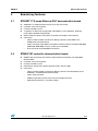
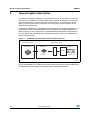
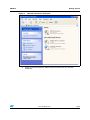
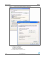
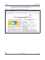
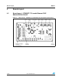
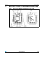
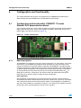
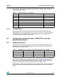
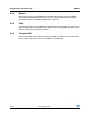
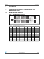
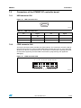
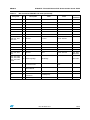
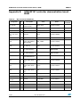
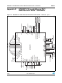
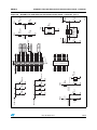
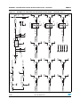
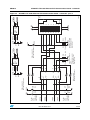
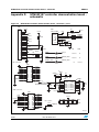
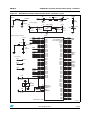
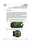
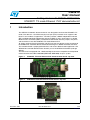
UM0819
User manual
Getting started with STEVAL-PCC010V1,
ST802RT1 TX mode Ethernet PHY demonstration kit
1
Introduction
The STEVAL-PCC010V1 demonstration kit was designed to evaluate the ST802RT1 TX
mode. This device is a Fast Ethernet physical layer (PHY) interface which supports 100
Base-TX and 10 Base-T applications. The PHY provides a Media Independent Interface
(MII) and Reduced Media Independent Interface (RMII) for easy attachment to a 10/100
Media Access Controllers (MAC). The demonstration board features jumpers, test points
and connectors to test the ST802RT1 TX mode Ethernet PHY.
To quickly evaluate the microcontroller and physical layer, the device can be connected to
the STM32F107 controller demonstration board through an additional header connector.
The controller board is preprogrammed with a web server demonstration application. The
STM32F107 controller demonstration board is part of the STEVAL-PCC010V1 package
delivery.
The board can be equipped with a dedicated digital connector compatible to the Spirent®
Communications SmartBits 200/2000 (SMB-200/ SMB-2000) analysis system.
Figure 1.
ST802RT1 TX mode Ethernet PHY demonstration board - top view
Figure 2.
STM32F107 controller demonstration board - top view
November 2009
Doc ID 16379 Rev 1
1/36
www.st.com
UM0819
Contents
Contents
1
Introduction . . . . . . . . . . . . . . . . . . . . . . . . . . . . . . . . . . . . . . . . . . . . . . . . 1
2
Boards key features . . . . . . . . . . . . . . . . . . . . . . . . . . . . . . . . . . . . . . . . . 6
2.1
ST802RT1 TX mode Ethernet PHY demonstration board . . . . . . . . . . . . . 6
2.2
STM32F107 controller demonstration board . . . . . . . . . . . . . . . . . . . . . . . 6
3
General system description . . . . . . . . . . . . . . . . . . . . . . . . . . . . . . . . . . . 7
4
Getting started . . . . . . . . . . . . . . . . . . . . . . . . . . . . . . . . . . . . . . . . . . . . . . 8
5
6
4.1
Package contents . . . . . . . . . . . . . . . . . . . . . . . . . . . . . . . . . . . . . . . . . . . . 8
4.2
How to run the demonstration software . . . . . . . . . . . . . . . . . . . . . . . . . . . 8
Boards layout . . . . . . . . . . . . . . . . . . . . . . . . . . . . . . . . . . . . . . . . . . . . . . 13
5.1
Board layout - ST802RT1 TX mode Ethernet PHY demonstration
board . . . . . . . . . . . . . . . . . . . . . . . . . . . . . . . . . . . . . . . . . . . . . . . . . . . . 13
5.2
Board layout - STM32F107 controller demonstration board . . . . . . . . . . . 14
Configuration and functionality . . . . . . . . . . . . . . . . . . . . . . . . . . . . . . . 15
6.1
6.2
Configuration and functionality- ST802RT1 TX mode Ethernet PHY
demonstration board . . . . . . . . . . . . . . . . . . . . . . . . . . . . . . . . . . . . . . . . 15
6.1.1
Boot strap options . . . . . . . . . . . . . . . . . . . . . . . . . . . . . . . . . . . . . . . . . 15
6.1.2
Solder bridges . . . . . . . . . . . . . . . . . . . . . . . . . . . . . . . . . . . . . . . . . . . . 17
6.1.3
RESET button . . . . . . . . . . . . . . . . . . . . . . . . . . . . . . . . . . . . . . . . . . . . 17
6.1.4
LEDs . . . . . . . . . . . . . . . . . . . . . . . . . . . . . . . . . . . . . . . . . . . . . . . . . . . 17
6.1.5
Test point MCO . . . . . . . . . . . . . . . . . . . . . . . . . . . . . . . . . . . . . . . . . . . 18
Configuration and functionality - STM32F107 controller demonstration
board . . . . . . . . . . . . . . . . . . . . . . . . . . . . . . . . . . . . . . . . . . . . . . . . . . . . 18
6.2.1
MII/RMII configuration . . . . . . . . . . . . . . . . . . . . . . . . . . . . . . . . . . . . . . 18
6.2.2
Buttons . . . . . . . . . . . . . . . . . . . . . . . . . . . . . . . . . . . . . . . . . . . . . . . . . . 19
6.2.3
LEDs . . . . . . . . . . . . . . . . . . . . . . . . . . . . . . . . . . . . . . . . . . . . . . . . . . . 19
6.2.4
Test point MCO . . . . . . . . . . . . . . . . . . . . . . . . . . . . . . . . . . . . . . . . . . . 19
Doc ID 16379 Rev 1
2/36
Contents
7
UM0819
Connectors . . . . . . . . . . . . . . . . . . . . . . . . . . . . . . . . . . . . . . . . . . . . . . . 20
7.1
7.2
Connectors of the ST802RT1 TX mode Ethernet PHY demonstration
board . . . . . . . . . . . . . . . . . . . . . . . . . . . . . . . . . . . . . . . . . . . . . . . . . . . . 20
7.1.1
MII/RMII debugging connector J1 . . . . . . . . . . . . . . . . . . . . . . . . . . . . . 20
7.1.2
MII/RMII connector P1 . . . . . . . . . . . . . . . . . . . . . . . . . . . . . . . . . . . . . . 21
7.1.3
RJ45 connector J9 . . . . . . . . . . . . . . . . . . . . . . . . . . . . . . . . . . . . . . . . . 21
Connectors of the STM32F107 controller board . . . . . . . . . . . . . . . . . . . 22
7.2.1
USB connector CN1 . . . . . . . . . . . . . . . . . . . . . . . . . . . . . . . . . . . . . . . 22
7.2.2
JTAG connector CN2 . . . . . . . . . . . . . . . . . . . . . . . . . . . . . . . . . . . . . . . 22
7.2.3
MII/RMII connector CN3 . . . . . . . . . . . . . . . . . . . . . . . . . . . . . . . . . . . . 23
7.2.4
GPIO connector CN4 . . . . . . . . . . . . . . . . . . . . . . . . . . . . . . . . . . . . . . . 24
Appendix A ST802RT1 TX mode Ethernet PHY demonstration board
- BOM . . . . . . . . . . . . . . . . . . . . . . . . . . . . . . . . . . . . . . . . . . . . . . . . . 25
Appendix B STM32F107 controller demonstration board - BOM . . . . . . . . . . . . 27
Appendix C ST802RT1 TX mode Ethernet PHY demonstration board
- schematic . . . . . . . . . . . . . . . . . . . . . . . . . . . . . . . . . . . . . . . . . . . . . 29
Appendix D STM32F107 controller demonstration board - schematic . . . . . . . 33
8
3/36
Revision history . . . . . . . . . . . . . . . . . . . . . . . . . . . . . . . . . . . . . . . . . . . 35
Doc ID 16379 Rev 1
UM0819
List of tables
List of tables
Table 1.
Table 2.
Table 3.
Table 4.
Table 5.
Table 6.
Table 7.
Table 8.
Table 9.
Table 10.
Table 11.
Table 12.
Table 13.
Table 14.
Table 15.
Table 16.
Table 17.
Table 18.
Table 19.
Auto-negotiation jumper settings . . . . . . . . . . . . . . . . . . . . . . . . . . . . . . . . . . . . . . . . . . . . 16
PHY MII address jumper settings . . . . . . . . . . . . . . . . . . . . . . . . . . . . . . . . . . . . . . . . . . . . 16
Power-down jumper settings . . . . . . . . . . . . . . . . . . . . . . . . . . . . . . . . . . . . . . . . . . . . . . . 16
Loopback jumper setting. . . . . . . . . . . . . . . . . . . . . . . . . . . . . . . . . . . . . . . . . . . . . . . . . . . 17
MII/RMII jumper settings . . . . . . . . . . . . . . . . . . . . . . . . . . . . . . . . . . . . . . . . . . . . . . . . . . . 17
MII/RMII interface selection . . . . . . . . . . . . . . . . . . . . . . . . . . . . . . . . . . . . . . . . . . . . . . . . 17
LEDs functionality - alternative 1 . . . . . . . . . . . . . . . . . . . . . . . . . . . . . . . . . . . . . . . . . . . . 17
LEDs functionality - alternative 2 . . . . . . . . . . . . . . . . . . . . . . . . . . . . . . . . . . . . . . . . . . . . 18
MII/RMII interface selection by solder bridges SB1, SB2 and SB3. . . . . . . . . . . . . . . . . . . 18
MII/RMII debugging connector J1 . . . . . . . . . . . . . . . . . . . . . . . . . . . . . . . . . . . . . . . . . . . . 20
MII/RMII connector P1 . . . . . . . . . . . . . . . . . . . . . . . . . . . . . . . . . . . . . . . . . . . . . . . . . . . . 21
RJ45 connector J9 . . . . . . . . . . . . . . . . . . . . . . . . . . . . . . . . . . . . . . . . . . . . . . . . . . . . . . . 21
USB connector CN1 . . . . . . . . . . . . . . . . . . . . . . . . . . . . . . . . . . . . . . . . . . . . . . . . . . . . . . 22
JTAG connector CN2 . . . . . . . . . . . . . . . . . . . . . . . . . . . . . . . . . . . . . . . . . . . . . . . . . . . . . 23
MII/RMII connector CN3 . . . . . . . . . . . . . . . . . . . . . . . . . . . . . . . . . . . . . . . . . . . . . . . . . . . 24
GPIO connector CN4 . . . . . . . . . . . . . . . . . . . . . . . . . . . . . . . . . . . . . . . . . . . . . . . . . . . . . 24
Bill of material ST802RT1 TX mode . . . . . . . . . . . . . . . . . . . . . . . . . . . . . . . . . . . . . . . . . . 25
Bill of material STM32F107 . . . . . . . . . . . . . . . . . . . . . . . . . . . . . . . . . . . . . . . . . . . . . . . . 27
Document revision history . . . . . . . . . . . . . . . . . . . . . . . . . . . . . . . . . . . . . . . . . . . . . . . . . 35
Doc ID 16379 Rev 1
4/36
List of figures
UM0819
List of figures
Figure 1.
Figure 2.
Figure 3.
Figure 4.
Figure 5.
Figure 6.
Figure 7.
Figure 8.
Figure 9.
Figure 10.
Figure 11.
Figure 12.
Figure 13.
Figure 14.
Figure 15.
Figure 16.
Figure 17.
Figure 18.
Figure 19.
Figure 20.
Figure 21.
Figure 22.
Figure 23.
Figure 24.
5/36
ST802RT1 TX mode Ethernet PHY demonstration board - top view . . . . . . . . . . . . . . . . . . 1
STM32F107 controller demonstration board - top view . . . . . . . . . . . . . . . . . . . . . . . . . . . . 1
ST802RT1 TX mode Ethernet PHY demonstration kit . . . . . . . . . . . . . . . . . . . . . . . . . . . . 7
ST802RT1 TX mode demonstration board connected to STM32F107 demonstration
board. . . . . . . . . . . . . . . . . . . . . . . . . . . . . . . . . . . . . . . . . . . . . . . . . . . . . . . . . . . . . . . . . . . 9
Network connections dialog box . . . . . . . . . . . . . . . . . . . . . . . . . . . . . . . . . . . . . . . . . . . . . 10
Internet Protocol (TCP/IP) Properties dialog box . . . . . . . . . . . . . . . . . . . . . . . . . . . . . . . . 11
First page of the web server demonstration software . . . . . . . . . . . . . . . . . . . . . . . . . . . . . 12
Board layout - ST802RT1 TX mode Ethernet PHY demonstration board. . . . . . . . . . . . . . 13
Board layout - STM32F107 controller demonstration board . . . . . . . . . . . . . . . . . . . . . . . . 14
Jumper configuration . . . . . . . . . . . . . . . . . . . . . . . . . . . . . . . . . . . . . . . . . . . . . . . . . . . . . 15
MII/RMII debugging connector J1 . . . . . . . . . . . . . . . . . . . . . . . . . . . . . . . . . . . . . . . . . . . . 20
MII/RMII connector P1 . . . . . . . . . . . . . . . . . . . . . . . . . . . . . . . . . . . . . . . . . . . . . . . . . . . . 21
Ethernet RJ45 connector J9 - front view. . . . . . . . . . . . . . . . . . . . . . . . . . . . . . . . . . . . . . . 21
USB connector CN1 . . . . . . . . . . . . . . . . . . . . . . . . . . . . . . . . . . . . . . . . . . . . . . . . . . . . . . 22
JTAG connector CN2 . . . . . . . . . . . . . . . . . . . . . . . . . . . . . . . . . . . . . . . . . . . . . . . . . . . . . 22
JTAG connector CN2 - schematic . . . . . . . . . . . . . . . . . . . . . . . . . . . . . . . . . . . . . . . . . . . 23
MII/RMII connector CN3 . . . . . . . . . . . . . . . . . . . . . . . . . . . . . . . . . . . . . . . . . . . . . . . . . . . 23
GPIO connector CN4 . . . . . . . . . . . . . . . . . . . . . . . . . . . . . . . . . . . . . . . . . . . . . . . . . . . . . 24
ST802RT1 TX mode Ethernet PHY demonstration board - schematic - part 1 . . . . . . . . . 29
ST802RT1 TX mode Ethernet PHY demonstration board - schematic - part 2 . . . . . . . . . 30
ST802RT1 TX mode Ethernet PHY demonstration board - schematic - part 3 . . . . . . . . . 31
ST802RT1 TX mode Ethernet PHY demonstration board - schematic - part 4 . . . . . . . . . 32
STM32F107 controller demonstration board - schematic - part 1. . . . . . . . . . . . . . . . . . . . 33
STM32F107 controller demonstration board - schematic - part 2. . . . . . . . . . . . . . . . . . . . 34
Doc ID 16379 Rev 1
UM0819
Boards key features
2
Boards key features
2.1
ST802RT1 TX mode Ethernet PHY demonstration board
2.2
●
ST802RT1 TX mode Fast Ethernet physical layer transceiver
●
On-board 3.3 V LDO regulator
●
On-board 25 MHz crystal
●
12 jumpers for boot-strap configuration (MII address, auto-negotiation, loopback,
power-down, MII/RMII configuration)
●
Several GND test points and jumpers for power consumption measurement
●
Connectors
–
20-pin full pitch header connector for debug purposes (compatible to the
STM32F107 controller board)
–
40-pin connector compatible to the Spirent Communications SmartBits 200/2000
(SMB-200/ SMB-2000) analysis system (not assembled)
–
RJ45 connector with embedded transformer
STM32F107 controller demonstration board
●
STM32F107 connectivity line Cortex™-M3 based microcontroller with embedded
Ethernet MAC
●
On-board 3.3 V LDO regulator
●
On-board 25 MHz crystal
●
Reset button, power LED, general-purpose button and two LEDs
●
Connectors
–
20-pin full pitch header connector for debug purposes and compatibility to the
ST802RT1 TX mode demonstration board
–
20-pin JTAG connector
–
Additional general-purpose 20-pin full pitch header connector
–
USB device connector (+5 V power supply)
Doc ID 16379 Rev 1
6/36
General system description
3
UM0819
General system description
The STEVAL-PCC010V1 ST802RT1 TX mode Ethernet PHY demonstration kit consists of
two boards. The ST802RT1 TX mode demonstration board was designed to evaluate the
chip. It therefore allows to easily select the PHY boot options, to evaluate the PHY boot
options, to evaluate the power consumption of the chip and to attach the device to the
professional test equipment.
In addition, the STM32F107 controller demonstration board can extend the ST802RT1 TX
mode demonstration board with STM32™ microcontroller and its embedded MAC. This
allows to quickly evaluate application on the embedded microcontroller and the Ethernet
PHY. By default, the controller board is preprogrammed with a web-server application for
demonstration purposes.
Figure 3.
ST802RT1 TX mode Ethernet PHY demonstration kit
STM32F107
demonstration board
STM32F107
ST802RT1 TX mode
demonstration board
ST802RT1
Transformer
10 Base-T
RJ45
TQFP48
100 Base-TX
AM00638
Figure 3 shows the ST802RT1 TX mode Ethernet PHY demonstration kit. It consists of two
boards: the ST802RT1 TX mode Ethernet PHY demonstration board, and the STM32F107
controller demonstration board connected through the MII/RMII connector.
7/36
Doc ID 16379 Rev 1
UM0819
4
Getting started
Getting started
This section briefly describes how to start using the STEVAL-PCC010V1 ST802RT1 TX
mode Ethernet PHY demonstration kit. To use this demonstration kit you must install
a web browser on your computer.
4.1
Package contents
The ST802RT1 TX mode Ethernet PHY demonstration kit includes the following items:
Hardware content
●
One ST802RT1 TX mode Ethernet PHY demonstration board
●
One STM32F107 controller demonstration board
Software content
●
Web server - demonstration software based on uIP TCP/IP stack
Documentation
4.2
●
STM32F107xx datasheet, ST802RT1 product documentation
●
This user manual
How to run the demonstration software
This section describes the demonstration software delivered with the ST802RT1 TX mode
Ethernet PHY demonstration kit. The software implements a simple web server based on
uIP TCP/IP stack. The web server consists of three pages displaying general information
about the STM32 and ST802RT1 TX mode, allowing to control LEDs on the STM32F107
controller board and finally showing the content of the ST802RT1 TX mode registers.
To run the demonstration software, you need a demonstration kit, an Ethernet cable, and
a PC with a web browser.
Follow the steps below:
1.
Connect the boards delivered in the package as shown on the Figure 4.
Doc ID 16379 Rev 1
8/36
Getting started
UM0819
Figure 4.
2.
Setup properly jumpers on the ST802RT1 TX mode Ethernet PHY demonstration
board. The software does not change any settings of the PHY; it reads the settings
from the PHY instead. See Section 6.1 for more details about board setup.
3.
Connect ST802RT1 TX mode Ethernet PHY board to STM32F107 controller board.
4.
Connect Ethernet cable to the ST802RT1 TX mode Ethernet PHY board on one side
and to the PC on the other side.
5.
Flash the demonstration software into the Flash memory of the STM32F107 MCU.
6.
Configure your PC. The following description is valid for Windows® XP; nevertheless
it is easy to setup any other operating system in a similar way.
a)
9/36
ST802RT1 TX mode demonstration board connected to STM32F107
demonstration board
Setup network settings: In Control Panel - Network Connections right click your
network card and open Properties.
Doc ID 16379 Rev 1
UM0819
Getting started
Figure 5.
b)
Network connections dialog box
Select IP protocol properties: Select Internet Protocol (TCP/IP) and click
Properties.
Doc ID 16379 Rev 1
10/36
Getting started
UM0819
Figure 6.
c)
Internet Protocol (TCP/IP) Properties dialog box
Change you IP settings to:
IP address: 192.168.0.4
Subnet mask: 255.255.255.0
d)
11/36
Disable firewall(s) running on your PC.
Doc ID 16379 Rev 1
UM0819
Getting started
7.
Figure 7.
Run your web browser and open page http://192.168.0.8. You should be able to see the
first page of the web server running on the demonstration kit.
First page of the web server demonstration software
8.
You can also ping to the board using ping command on your PC.
Doc ID 16379 Rev 1
12/36
Boards layout
UM0819
5
Boards layout
5.1
Board layout - ST802RT1 TX mode Ethernet PHY
demonstration board
Figure 8.
13/36
Board layout - ST802RT1 TX mode Ethernet PHY demonstration board
Doc ID 16379 Rev 1
UM0819
5.2
Boards layout
Board layout - STM32F107 controller demonstration board
Figure 9.
Board layout - STM32F107 controller demonstration board
Doc ID 16379 Rev 1
14/36
Configuration and functionality
6
UM0819
Configuration and functionality
This section describes the functions and configuration of STM802RT1A Ethernet PHY
demonstration board and STM32F107 controller demonstration board.
6.1
Configuration and functionality- ST802RT1 TX mode
Ethernet PHY demonstration board
In this chapter jumper “high” means that the jumper is placed in the position closer to the top
edge of the board and “low” means that the jumper is placed in the position closer to the
bottom edge of the board as shown by Figure 10.
Figure 10. Jumper configuration
6.1.1
Boot strap options
The ST802RT1 TX mode PHY uses many of the functional pins as strap options. The values
of these pins are sampled during hardware reset and power up. They are used to strap
signals on the device into specific modes of operation. The ST802RT1 TX mode provides
a simple strap option to automatically configure the device to operate in the modes requiring
no device register configuration. All strap pins have a weak internal pull-ups or pull-downs.
To change the default strap value, the strap pins should be connected directly to VCC or
GND with an external 2.2 kΩ resistor. The software reset and power-down through the
power-down pin cannot be used to change the strap configuration.
Auto-negotiation
Auto-negotiation is performed as part of the initial set-up of the link. It allows the PHYs
connected to the cable to exchange their key features (speed, PHY type, half or full duplex)
and automatically select the link communication mode. If auto-negotiation is disabled the
chip stays at the speed that is selected by strap pins. If the partner PHY speed is the same,
the link ON state is signaled otherwise no link state is signaled.
15/36
Doc ID 16379 Rev 1
UM0819
Configuration and functionality
Table 1.
Auto-negotiation jumper settings(1)
Jumper
Description
Default configuration
JP16
AN_1
High
JP17
AN_0
High
JP18
AN_EN - Auto-negotiation enable; when “high” - autonegotiation enabled, when “low” - auto-negotiation disabled
High
1. See functionality of AN_xxx pins in the ST802RT1 product documentation.
PHY MII address
The MDIO/MDC serial management interface is used to access the internal registers of the
PHY. The Ethernet MAC that is connected to the PHY must know the appropriate PHY
address for successful communication. Special case is the PHY address 0x00. If this
address is used as the bootstrap address during the reset, the 00000 value is latched into
the internal receive mode control register RN14 (0x14h) but the PHY goes also to the
isolation mode. It is possible to change the PHY address by writing the RN14 register later
when application is already running.
Table 2.
PHY MII address jumper settings
Jumper
Description
Default configuration
JP11
MII address 0
High
JP12
MII address 1
Low
JP13
MII address 2
Low
JP14
MII address 3
Low
JP15
MII address 4
Low
Power-down
This pin is an active low input of the PHY and should be asserted low to put the device in
a power-down mode. During the power-down mode, TXP/TXN outputs and all LED outputs
are 3-stated, and the MII interface is isolated. The power-down functionality is also
achievable by software by asserting bit 11 of register RN00.
Table 3.
Power-down jumper settings
Jumper
Description
Default configuration
JP1
Power-down, if fitted - PHY works normally; if not fitted - PHY is
in power-down mode
Fitted
Loopback
Local loopback passes data internally from the transmitting to the receiving serial analog
logic. There are two ways to enter the internal loopback mode, either writing RN00 register,
bit 14 (MDIO/MDC) or by using boot strap LPBK pin (VDD - enabled, GND - disabled,
through 2.2 kΩ resistor).
Doc ID 16379 Rev 1
16/36
Configuration and functionality
Table 4.
UM0819
Loopback jumper setting
Jumper
Description
Default configuration
JP8
LPBK - loopback; “high” - internal loopback selected (mainly for
debug purposes); “low” - normal operation
Low
MII/RMII mode selection
A strapping option allows setting the operating mode of the MAC data interface. Default
operation (no pull-ups) enable normal MII mode of operation. Strapping CF0 high will cause
the device to be in RMII.
Table 5.
Jumper
Description
Default configuration
JP9
CF0 - MAC data interface selection
Low
JP10
CF1 - MAC data interface selection
Low
Table 6.
6.1.2
MII/RMII jumper settings
MII/RMII interface selection
CF0 (JP9)
CF1 (JP10)
MII
Low
X
RMII
High
Low
Solder bridges
The SB1 and SB2 solder bridges are used to connect 25MHz crystal X1 to the ST802RT1
TX mode PHY. They can be removed to disconnect the crystal when external clock signal on
test point MCO is used as the input clock.
6.1.3
RESET button
The RESET button resets the ST802RT1 TX mode PHY to its initial state.
6.1.4
LEDs
By default the LEDs have the following functionality:
Table 7.
17/36
LEDs functionality - alternative 1
LED
Description
Details
LED1
BLINK for activity
JP16 is low
LED2
BLINK for activity
JP16 is high
LED3
ON for 100 Mb / OFF for 10 Mb
JP17 is low
LED4
ON for 100 Mb / OFF for 10 Mb
JP17 is high
LED5
ON for link up / OFF for link down
JP18 is low
LED6
ON for link up / OFF for link down
JP18 is high
Doc ID 16379 Rev 1
UM0819
Configuration and functionality
Alternatively it is possible to change the meaning of LED1 - LED6 by writing the PHY
register RN1B [0d27, 0x1B]:
Table 8.
6.1.5
LEDs functionality - alternative 2
LED
Description
Details
LED1
ON for full duplex, BLINK for collision
JP16 is low
LED2
ON for full duplex, BLINK for collision
JP16 is high
LED3
ON for 100 Mb / OFF for 10 Mb
JP17 is low
LED4
ON for 100 Mb / OFF for 10 Mb
JP17 is high
LED5
ON for link up and BLINK for activity / OFF for link down
JP18 is low
LED6
ON for link up and BLINK for activity / OFF for link down
JP18 is high
LED8
Is used for indicating that the board is powered
—
Test point MCO
The test point MCO can be used to connect external clock signal to clock input of the
STM802RT1A PHY in MII mode. Note that the 25 MHz crystal X1 has to be disconnected
from the ST802RT1 TX mode PHY by removing solder bridges SB1 and SB2 before
connecting any external signal to the test point.
6.2
Configuration and functionality - STM32F107 controller
demonstration board
6.2.1
MII/RMII configuration
The STM32F107 controller demonstration board can be configured to communicate with
Ethernet PHY using either MII or RMII interface. The configuration is done using three
solder bridges SB1, SB2 and SB3.
Table 9.
MII/RMII interface selection by solder bridges SB1, SB2 and SB3
SB1
SB2
SB3
MII
Remove
Remove
Fit
RMII
Fit
Fit
Remove
In MII mode, the ST802RT1 TX mode Ethernet PHY demonstration board can be clocked
either from its on-board 25 MHz crystal oscillator or by the 25 MHz clock signal output MCO from the STM32F107 controller demonstration board, see Section 6.1.5 and 6.2.4.
Both MCO pins (test points) must be interconnected by an additional wire.
In RMII mode, the ST802RT1 TX mode Ethernet PHY demonstration board is clocked from
the 50 MHz clock signal output delivered from the STM32F107 controller demonstration
board.
Doc ID 16379 Rev 1
18/36
Configuration and functionality
6.2.2
UM0819
Buttons
There are two buttons on the STM32F107 controller demonstration board. The RESET
button resets the STM32F107 MCU to its initial state. The B1 general purpose button is
connected to PA4-pin of STM32F107 MCU and is active low.
6.2.3
LEDs
There are three LEDs on the STM32F107 controller demonstration board. LD1 and LD2 are
general purpose LEDs connected to PC13 and PC14-pins of the STM32F107 MCU. LD3 is
used for indicating that the board is powered.
6.2.4
Test point MCO
There is MCO (Main Clock Output) clock signal of STM32 available on this test point which
can be used as input clock source of the ST802RT1 TX mode PHY.
19/36
Doc ID 16379 Rev 1
UM0819
Connectors
7
Connectors
7.1
Connectors of the ST802RT1 TX mode Ethernet PHY
demonstration board
7.1.1
MII/RMII debugging connector J1
Figure 11. MII/RMII debugging connector J1
1 2 3 4
5 6
8 9 10 11 12 13 14 15 16 17 18 19 20
42
41
21 22 23 24 25 26 27 28 29 30 31 32 33 34 35 36 37 38 39 40
AM00639
Table 10.
MII/RMII debugging connector J1
Pin
Signal
Pin
Signal
Pin
Signal
Pin
Signal
1
+5 V
12
TXCLK
23
GND
34
GND
2
MDIO
13
TXEN
24
GND
35
GND
3
MDC
14
TXD_0
25
GND
36
GND
4
RXD_3
15
TXD_1
26
GND
37
GND
5
RXD_2
16
TXD_2
27
GND
38
GND
6
RXD_1
17
TXD_3
28
GND
39
GND
7
RXD_0
18
COL
29
GND
40
Not connected
8
RXDV
19
CRS
30
GND
41
GND
9
RXCLK
20
Not connected
31
GND
42
GND
10
RXER
21
+5 V
32
GND
11
TXER
22
GND
33
GND
Doc ID 16379 Rev 1
20/36
Connectors
7.1.2
UM0819
MII/RMII connector P1
Figure 12. MII/RMII connector P1
2
4
6
8 10 12 14 16 18 20
1
3
5
7
9 11 13 15 17 19
AM00640
Table 11.
7.1.3
MII/RMII connector P1
Pin
Signal
Pin
Signal
Pin
Signal
Pin
Signal
1
GND
6
RXD3
11
TXER
16
TXD0
2
+5 V
7
RXD0
12
RXER
17
TXD3
3
MDC
8
RXD1
13
TXEN
18
TXD2
4
MDIO
9
RXCLK
14
TXCLK
19
CRS
5
RXD2
10
RXDV
15
TXD1
20
COL
RJ45 connector J9
Figure 13. Ethernet RJ45 connector J9 - front view
Table 12.
21/36
RJ45 connector J9
Pin
Description
Pin
Description
1
TxData+
2
TxData–
3
RxData+
4
NC
5
NC
6
RxData–
7
NC
8
NC
Doc ID 16379 Rev 1
UM0819
Connectors
7.2
Connectors of the STM32F107 controller board
7.2.1
USB connector CN1
Figure 14. USB connector CN1
AM00642
Table 13.
7.2.2
USB connector CN1
Pin
Signal
Pin
Signal
1
VBUS
4
ID
2
D–
5
GND
3
D+
6
SH
JTAG connector CN2
The 20-pin connector (CN2) provides the JTAG interface. This interface is primarily used for
communicating with a PC using suitable USB/JTAG converter box such as J-Link from IAR
Systems™ or R-Link from Raisonance, etc. There exists a wide choice of development tools
on the market supporting microcontroller Flash memory programming and application
debugging.
Figure 15. JTAG connector CN2
2
4
6
8 10 12 14 16 18 20
1
3
5
7
9 11 13 15 17 19
AM00643
Doc ID 16379 Rev 1
22/36
Connectors
UM0819
Table 14.
JTAG connector CN2
Pin
Signal
Pin
Signal
Pin
Signal
Pin
Signal
1
3.3 V DC
6
GND
11
RTCK connected to
GND by R1 (10 kΩ)
16
GND
2
3.3 V DC
7
JTMS
12
GND
17
DBGRQ connected to
GND by R2 (10 kΩ)
3
JTRST
8
GND
13
JTDO
18
GND
4
GND
9
JTCK
14
GND
19
DBGACK connected to
GND by R14 (10 kΩ)
5
JTDI
10
GND
15
NRST
20
GND
Figure 16. JTAG connector CN2 - schematic
CN2
JTAG
3.3 V
1
2
3
4
5
6
7
8
9
10
11
12
13
14
15
16
17
18
19
20
JTRST internal pull-up
JTDI
internal pull-up
JTMS
internal pull-up
JTCK
internal pull-down
RTCK
JTDO
R1
10 KΩ
NRST
DBGRQ
R2
DBGACK
10 KΩ
R14
10 KΩ
AM00644
7.2.3
MII/RMII connector CN3
Figure 17. MII/RMII connector CN3
2
4
6
8 10 12 14 16 18 20
1
3
5
7
9 11 13 15 17 19
AM00640
23/36
Doc ID 16379 Rev 1
UM0819
Connectors
Table 15.
7.2.4
MII/RMII connector CN3
Pin
Signal
Pin
Signal
Pin
Signal
Pin
Signal
1
GND
6
RXD3
11
TXER
16
TXD0
2
+5 V
7
RXD0
12
RXER
17
TXD3
3
MDC
8
RXD1
13
TXEN
18
TXD2
4
MDIO
9
RXCLK
14
TXCLK
19
CRS
5
RXD2
10
RXDV
15
TXD1
20
COL
GPIO connector CN4
Figure 18. GPIO connector CN4
2
4
6
8 10 12 14 16 18 20
1
3
5
7
9 11 13 15 17 19
AM00645
Table 16.
GPIO connector CN4
Pin
Signal
Pin
Signal
Pin
Signal
Pin
Signal
1
GND
6
PD3
11
PD4
16
PE0
2
+5 V
7
+3.3 V
12
PC12
17
PD7
3
PA6
8
PA15
13
PD5
18
PE1
4
PD2
9
GND
14
PC7
19
GND
5
PA5
10
PC10
15
PD6
20
+3.3 V
Doc ID 16379 Rev 1
24/36
ST802RT1 TX mode Ethernet PHY demonstration board - BOM
Appendix A
Table 17.
UM0819
ST802RT1 TX mode Ethernet PHY
demonstration board - BOM
Bill of material ST802RT1 TX mode
Designator
Qty.
Description
B1
1
Push button (DT2112C)
RESET
GM Electronic®:
630-121
Farnell: 9471898
C1, C2
2
Capacitor
10 nF
Farnell: 1709948
C3, C4
2
Capacitor
12 pF
Farnell: 1462447
C5, C6, C7, C9,
C10, C11, C14,
C15, C17, C18,
C19
11
Capacitor
100 nF
Farnell: 4532004
C8, C12
2
Capacitor
Murata:
1 µF / X5R Murata
Manufacturing Co., Ltd. GRM188R60J105KA01
GRM188R60J105KA01 Farnell: 1710296
C13, C16
2
Polarized capacitor
10 µF / tantalum
Farnell: 1213794
D1
1
Schottky diode
STPS160A /
STPS2L40U
STMicroelectronics™:
STPS2L40U
J1
1
Plug assembly, 40-pin
connector
Connector 40
Tyco Electronics:
174218-2;
Fujitsu:
FCN-238P040-G/F
J2, J8
2
1-pin header, 2 mm
banana receptacle
2MM_REC
J3, J4, J5, J6, J7
5
1-pin header
GND
J9
1
RJ45 Ethernet connector
RJ-45
with integrated magnetic
Pulse: J00-0086NL
JP1, JP4, JP5,
JP6, JP7, JP19,
JP20
7
2-pin jumper wire
Jumper
Farnell: 1593411
JP8, JP9, JP10,
JP11, JP12,
JP13, JP14,
JP15, JP16,
JP17, JP18
11
3-pin jumper wire
Jumper3
Farnell: 1593412
L1, L2
2
Ferrite bead
NFE31PT222Z1E9L
Murata
Farnell: 9528172
LED1, LED2
2
LED
Yellow
Farnell: 1226420
LED3, LED4,
LED8
3
LED
Red
Farnell: 1226392
LED5, LED6
2
LED
Green
Farnell: 1226373
25/36
Value
Doc ID 16379 Rev 1
Order
Not
assembled
C10, C17
J1
J2, J8
Farnell: 1593411
UM0819
Table 17.
ST802RT1 TX mode Ethernet PHY demonstration board - BOM
Bill of material ST802RT1 TX mode (continued)
Designator
Qty.
Description
Value
Order
Not
assembled
P1
1
Header, 20-pin, dual row Header 10 x 2
Farnell: 1593446
R1
1
Resistor
5.6 KΩ
Farnell: 1514773
R2
1
Resistor
91 KΩ
Farnell: 1646361
R3, R4
2
Resistor
10 KΩ
Farnell: 1601277
R5
1
Resistor
1 MΩ NA
Farnell: 1631320
R5
R6, R8
2
Resistor
750 Ω
Farnell: 1399909
R6, R8
R7, R9
2
Resistor
1.2 KΩ
Farnell: 1632396
R17, R18, R19,
R20, R21, R22,
R23, R24
8
Resistor
2. 2 KΩ
Farnell: 1632417
R25
1
Resistor
330 Ω
Farnell: 1646224
R26, R28, R30
3
Resistor
2 KΩ
Farnell: 1632414
R27, R32
2
Resistor
470 Ω
Farnell: 9367659
R29
1
Resistor
220 Ω
Farnell: 1646159
R31, R33, R34,
R35
4
Resistor
75 Ω
Farnell: 9331549
SB1, SB2, SB3,
SB4, SB5, SB6,
SB7, SB8, SB9,
SB10
10
Soldering bridge
Soldbridge
U1
1
10 / 100 Fast Ethernet
3.3 V transceiver
ST802RT1 TX mode
ST: ST802RT1 TX
mode
U2, U5
2
ESD protection,
DALC208SC6
DVIULC6-2P6
ST: DVIULC6-2P6
U3
1
LD1117S33
ST: LD1117S33
U4
1
H1300 Ethernet
transformer
H1300 (pulse)
X1
1
Epson® Crystal: FA-238
25 MHz
Doc ID 16379 Rev 1
R31, R33,
R34, R35
SB4, SB5
Farnell: 1712818
26/36
STM32F107 controller demonstration board - BOM
Appendix B
Table 18.
UM0819
STM32F107 controller demonstration board BOM
Bill of material STM32F107
Designator
Qty.
Description
Value
Order
C1, C2, C8
3
Polarized capacitor
(surface mount)
10 µF / 6.3 V
Farnell: 1213794
C3, C4
2
Capacitor
100 nF_0805
Farnell: 1414664
C6, C17
2
Capacitor
100 nF_0603
Farnell: 4532004
C5, C7, C9, C10,
C11, C12, C13,
C14
8
Capacitor
10 nF
Farnell: 1709948
C15, C16
2
Capacitor
12 pF
Farnell: 1462447
CN1
1
Molex® - 675031020 socket, USB, MINI-B,
SMT, W/PEGS
USB_1X90A
Farnell: 1125348
CN2
1
Header, 20-pin, dual
row, with key
JTAG
Farnell: 1099258
CN3
1
Socket, 20-pin, dual
row, side mounting
Socket 10x2, BL820GD
Farnell: 1593494
GME:832-009
CN4
1
Socket, 20-pin, dual
row, side mounting
Socket 10x2, BL820GD
Farnell: 1593494
GME: 832-009
L1
1
Inductor,
BLM18BA05OSN1D
BEAD
Farnell: 1515680
LD1
1
Typical Red, Green,
Yellow, Amber GaAs
LED
Yellow
Farnell: 1226420
LD2
1
Typical Red, Green,
Yellow, Amber GaAs
LED
Green
Farnell: 1226373
LD3
1
Typical Red, Green,
Yellow, Amber GaAs
LED
Red
Farnell: 1226392
R1
1
Resistor
1. 5 kΩ_0603
Farnell: 1632406
R2, R4
2
Resistor
22 Ω_0603
Farnell: 1692521
R3, R6, R7, R8,
R9, R12
6
Resistor
10 kΩ_0603
Farnell: 1601277
R5
1
Resistor
1 MΩ_0603
Farnell: 1631320
R10
1
Resistor
47 Ω_0603
Farnell: 1646283
R11
1
Resistor
0 Ω_0603
Farnell: 1573911
R13
1
Resistor
330 Ω
Farnell: 1646224
27/36
Doc ID 16379 Rev 1
Not
assembled
R5
UM0819
Table 18.
STM32F107 controller demonstration board - BOM
Bill of material STM32F107 (continued)
Designator
Qty.
Description
Value
Order
R15
1
Resistor
470 Ω
Farnell: 9367659
R14
1
Resistor
220 Ω
Farnell: 1646159
RESET1
1
Switch
Reset
GME: 630-121 Farnell:
9471898
RESET2
1
Switch
B1
GME: 630-121 Farnell:
9471898
U2
1
MCU
STM32F107_256K
ST: STM32F107
U3
1
Low drop voltage
regulator
LD1117S33
ST: LD1117S33
X1
1
Epson Crystal: FA-238
25 MHz
Farnell: 1712818
SB1, SB2, SB3,
SB4
4
Solder bridge
Not
assembled
SB1, SB2
Doc ID 16379 Rev 1
28/36
29/36
Doc ID 16379 Rev 1
8
9
TXD_3
PWRDWN
GND
7
TXD_2
RDN
VCCA_CORE
12 GND
ST802RT1
RDP
RDP
RDN
GND
TDP
TDP
TDN
TDN
GND GND
IREF
SDP
RESET
MDIO
LED_ACT/AN1
LED_SPEED/AN0
VCCA_CORE
GND
13 14 15 16 17 18 19 20 21 22 23 24
33
34
35
36
LED_ACT/AN1
LED_ACT
AM00625
LED_SPEED
LED_SPEED/AN0
26
LED_LINK/AN_EN LED_LINK
27
SDP
RESET
MDIO
DVDD_CORE
MDC
GND
X2
DVDD_CORE
X1
28
25
29
30
OVDD 32
MDC 31
GND
X2
X1
LED_LINK/AN_EN
VCCA
GNDA VCCA
REF
GNDA
GNDA
VCCA RXN RXP TXP TXN GNDA I
PWRDWN/MDINT
TXD3/MII
_CFG1
TXD2/SCLK
TXD1
TXD0
VCCA
GNDA
TX_E N
10 RESERVED
11 RESERVED
6
5
4
TXD_1
VCCA_CORE
TXD_0
2
3
1
TXEN
Appendix C
TXCLK
47 46 45 44 43 42 41 48 40 39 38 37
RX_CLK
GND
RXDV/MII_CFG0
COL/PHYADDR0
CRS/TXD4
RXD0/PHYADDR1
RXERR/RXD4
RXD1/PHYADDR2
RXD2/PHYADDR3
SDN
TX_CLK/LP BK_EN
DVDD
RXD3/PHYADDR4 DVDD
U1
ST802RT1
TX mode
SDN
RXER
CRS
RXDV
RXCLK
DVDD_CORE
RXD_2 RXD_3
RXD_1
RXD_0
COL
GND
ST802RT1 TX mode Ethernet PHY demonstration board - schematic
UM0819
ST802RT1 TX mode Ethernet PHY
demonstration board - schematic
Figure 19. ST802RT1 TX mode Ethernet PHY demonstration board - schematic - part 1
Doc ID 16379 Rev 1
GND
R4
10 KΩ
PWRDWN
JP1
DVDD
VCCA_CORE
DVDD_CORE
GND
GND
C11
C12
100 nF 1 µF/X5R
RESET
GND
GND
C2
10 nF
GND
GND
C1
10 nF
1
2
GND
GND
R3
10 KΩ
DVDD
GND
B1
RESET
C5
C6
C7
C8
100 nF 100 nF 100 nF 1 µF/X5R
GND
C9
100 nF
+5 V
GND
MDC
RXD_ 2
RXD_ 0
RXCL K
TXER
TXEN
TXD_ 1
TXD_ 3
CRS
+5 V
GND
GND
GND
GND
GND
GND
GND
GND
GND
GND
GND
GND
GND
GND
GND
GND
GND
GND
1
2
3
4
5
6
7
8
9
10
11
12
13
14
15
16
17
18
19
20
+5 V
MDIO
MDC
RXD_ 3
RXD_ 2
RXD_ 1
RXD_ 0
RXDV
RXCLK
RXER
TXER
TXCL K
TXEN
TXD_0
TXD_1
TXD_2
TXD_3
CO L
CRS
1
3
5
7
9
11
13
15
17
19
P1
2
4
6
8
10
12
14
16
18
20
+5 V
MDIO
RXD_ 3
RXD_ 1
RXDV
RXER
TXCL K
TXD_ 0
TXD_ 2
COL
J1
40
Connector
MII
42
Header 10 x 2
21
22
23
24
25
26
27
28
29
30
31
32
33
34
35
36
37
38
39
40
41
TXD_3
CO L
SB 3
TXCLK
RXD_ 3
RXD_ 2
RXD_ 1
RXD_ 0
RXDV
X2
GND
C3
12 pF
GND
SB1
GND
SDN
X1
GND
R1
5.6 KΩ
3
4
IREF
1 MΩ NA
GND
C4
12 pF
SB2
AM00626
GND
GND
X1
R9
1.2 KΩ
R8
750 Ω NA
VCCA
R2
91 KΩ
SDP
25 MHz
TSX-3225,
FA-238, 25 MHz
R5
2
1
GND
R7
1.2 KΩ
R6
750 Ω NA
VCCA
UM0819
ST802RT1 TX mode Ethernet PHY demonstration board - schematic
Figure 20. ST802RT1 TX mode Ethernet PHY demonstration board - schematic - part 2
30/36
31/36
Doc ID 16379 Rev 1
TXD_3
RXDV
TXCLK
L2
3.3 V L1
R18
2
2
2
2.2 KΩ
R19
2.2 KΩ
TXD_3
RXDV
R17
2.2 KΩ
TXCLK
GND
JP20
2
RXD_0
2
RXD_1
2
GND
JP10
1
2.2 KΩ
GND
JP13
1
3
3
RXD_1
DVDD
DVDD
JP12
1
GND
R22
2.2 KΩ
GND
JP9
1
3
3
RXD_0
DVDD
DVDD
JP11
1
GND
R21
2.2 KΩ
GND
JP8
1
3
R20
VCCA_CORE
+5 V
3
COL
JP7
JP5
DVDD_CORE
DVDD
COL
VCCA
DVDD
DVDD
JP6
NFE31PT222Z1E9L
GND
JP4
NFE31PT222Z1E9L
RXD_3
RXD_2
GND
GND
GND
GND
R24
1
3
J7
J6
J5
J4
LED_LINK
LED4
1
2
LED3
2
LED_LINK/AN_EN 1
2
2
220 Ω
R29
Green
LED6
1
2
LED5
R32
470 Ω
Red
2 LED8
AM00628
GND
1
JP18
3
DVDD
GND
1
JP17
3
DVDD
GND
1
JP16
3
DVDD
GND
2
470 Ω
R27
Red
R30 2 KΩ
2
R25
330 Ω
J8
J2
3.3 V
Yellow
LED2
1
2
LED1
R28 2 KΩ
2
1
LED_SPEED/AN0 1
LED_ACT/AN1
GND
3.3 V
3.3 V
R26 2 KΩ
C16
10 µF / 6.3 V
JP19
3.3 V LDO
GND GND
2
LED_ACT
C15
100 nF
1
LED_SPEED
GND
JP15
1
3
DVDD
GND
JP14
J3
2
2.2 KΩ
RXD_3
GND
2
2.2 KΩ
RXD_2
R23
DVDD
GND
1
C14
100 nF
U3 LD1117S33
3 V
VOUT 2
IN
4
GND VOUT
GND GND
C13
10 µF / 6.3 V 2
STPS 2L40U 1
D1
3.3 V
1
ST802RT1 TX mode Ethernet PHY demonstration board - schematic
UM0819
Figure 21. ST802RT1 TX mode Ethernet PHY demonstration board - schematic - part 3
Doc ID 16379 Rev 1
100 nF
NA
100 nF
NA
GND
C17
C10
GND
Solder
only
with
standalone
transformer
TDP_C
RX–
CT
RX+
TX–
CT
TX+
SB10
SB9
H1300 H1300 NA
RD–
CT
RD+
TD–
CT
TD+
U4
SB8
SB7
Solder only with
embedded transformer
8
7
6
2
1
TDN_ C
NA
NA
3
SB5
SB4
VCCA
RDN_C
RDP_C
Solder
only
with
standalone
transformer
VCCA
Solder only with
embedded transformer
9
10
11
14
R33
R34
R35
75 Ω NA
GND GND
Typically not needed
at all
Properly the resistor
should be in series
with capacitor
75 Ω NA
75 Ω NA
GND GND
Typically not needed
at all (termination for
unused lines)
75 Ω NA
8
7
6
5
4
3
2
15
13
GND GND
10 14
GND
GND
RD–
GND
GND
RD+
TD–
TD+
9
GND GND
DVIULC6-2P6
U5
RDP_C 4
3
I/O2
I/O2
5 VBUS GND 2
RDN_C 6 I/O1
I/O1 1
1
SB6
VCCA
100 nF
C19
VCCA
16
R31
TDN
TDP
Solder only with
embedded transformer
U2
VCCA TDP_C 4 I/O2
I/O2 3
5 VBUS GND 2
C18
TDN_C 6 I/O1
I/O1 1
100 nF
DVIULC6-2P6
8
7
6
5
4
3
2
1
RJ-45
J9
RJ-45
AM00629
RDN
RDP
UM0819
ST802RT1 TX mode Ethernet PHY demonstration board - schematic
Figure 22. ST802RT1 TX mode Ethernet PHY demonstration board - schematic - part 4
32/36
STM32F107 controller demonstration board - schematic
Appendix D
UM0819
STM32F107 controller demonstration board schematic
Figure 23. STM32F107 controller demonstration board - schematic - part 1
JTAG
USB device
CN2
JTAG
+3.3 V
1
2
3
4
5
6
7
8
9
10
11
12
13
14
15
16
17
18
19
20
+3.3 V
PB4
PA15
R1
CN1
USB_1X90A
USB_A
VBUS
D–
D+
ID
GND
SH
R6
10 kΩ
PA13
PA14
1
2
3
4
5
6
1.5 kΩ
22 Ω
R2
R4
PA10
MII
#RESET
10 kΩ
22 Ω
10 nF
R7
10 kΩ
R8
USBDN
USBDP
R5 1 MΩ
C5
PB3
+3.3 V
+5 V
MCO
RMII
TXD_2
remove
fit
remove
fit
fit
remove
SB1
R9
MCO
RXCLK_MCU
10 kΩ
SB2
RXCLK_MCU
RXCLK_PHY
MII connector
SB3
CN3
MDC
RXD_2
RXD_0
RXCLK_PHY
TXER
TXEN
TXD_1
TXD_3
SB4 CRS
1
3
5
7
9
11
13
15
17
19
2
4
6
8
10
12
14
16
18
20
+5 V
MDIO
RXD_3
RXD_1
RXDV
RXER
TXCLK
TXD_0
TXD_2
COL
VREF+
VDDA
R10
47 Ω
L1
Header 10X2 +3.3 V
BLM18BA05OSN1D
C8
10 µF
/6.3 V
C9
10 nF
Audio connector
+3.3 V
21
22
50
75
100
28
11
6
CN4
PA6
PA5
+3.3 V
PD4
PD5
PD6
PD7
1
3
5
7
9
11
13
15
17
19
2
4
6
8
10
12
14
16
18
20
+5 V
PD2
PD3
PA15
PC10
PC12
PC7
PE0
PE1
+3.3 V
C7
10 nF
U2B
VREF+
VDDA
VDD_ 1
VDD_ 2
VDD_ 3
VDD_ 4
VDD_ 5
VBAT
VREF–
VREF–
VSSA
VSS_1
VSS_2
VSS_3
VSS_4
VSS_5
20
19
49
74
99
27
10
R11
0Ω
STM32F107_256K
+3.3 V
C10
Boot option
R12
C11
C12
C13
C14
10 nF 10 nF 10 nF 10 nF 10 nF
BOOT0
10 kΩ
Header 10X2 S
AM00631
33/36
Doc ID 16379 Rev 1
UM0819
STM32F107 controller demonstration board - schematic
Figure 24. STM32F107 controller demonstration board - schematic - part 2
LD2
+3.3 V
Reset
LED1
#RESET
LD1
2
1
R13
330 Ω
RESET1
C6
100 nF
Power supply
U3
3
C1
10 µF
/ 6.3 V
VIN
C3
100 nF
LD1117S33
VOUT 2
VOUT 4
GND
1
General purpose button
+3.3 V
1
2
LED2
220 Ω
R15
470 Ω
Green
Yellow
+5 V
R14
1
+3.3 V
Red
C4
100 nF
C2
10 µF
/ 6.3 V
LD3
2
U2A
CRS
RXCLK_MCU
MDIO
COL
#BUTTON
+3.3 V
PA0
PA2
PA3
10 kΩ
R3
PA4
PA5
#BUTTON
PA6
PA7
PA8
MCO
C17
PA9
100 nF
PA10
USBDN PA11
USBDP PA12
PA13
PA14
PA15
Test points
PB0
TP1
PB1
+3.3 V
PB2
+3.3 V
PB3
TP2
PB4
+5 V
PB5
+5 V
PB6
PB7
TP3
TXD_3 PB8
PB9
GND
PB10
RXER
PB11
TXEN
TXD_0 PB12
TXD_1 PB13
PB14
C15
PB15
23
24
25
26
29
30
31
32
67
68
69
70
71
72
76
77
35
36
37
89
90
91
92
93
95
96
47
48
51
52
53
54
12 pF
4
3
X1
25 MHz
FA-238
1
2
#RESET
C16
BOOT0
12
13
14
73
94
12 pF
PA 0-WKUP PC15-OSC32_OUT
PA 1
PC14-OSC32_I N
PA 2
PC13-ANTI_TAMP
PA 3
P C12
PA 4
P C11
PA 5
P C10
PA 6
PC9
PA 7
PC8
PA 8
PC7
PA 9
PC6
PA10
PC5
PA11
PC4
PA12
PC3
PA13
PC2
PA14
PC1
PA15
PC0
PB 0
PD15
PB 1
PD14
PB 2
PD13
PB 3
PD12
PB 4
PD11
PB 5
PD10
PB 6
PD9
PB 7
PD8
PB 8
PD7
PB 9
PD6
PB10
PD5
PB11
PD4
PB12
PD3
PB13
PD2
PB14
PD1
PB15
PD0
PE15
PE14
PE13
PE12
PE11
OSC_IN
PE10
OSC_OUT
PE9
NRST
PE8
NC
PE7
BOOT0
PE6
PE5
PE4
PE3
PE2
PE1
PE0
STM32F107_256K
Doc ID 16379 Rev 1
9
8
7
80
79
78
66
65
64
63
34
33
18
17
16
15
62
61
60
59
58
57
56
55
88
87
86
85
84
83
82
81
46
45
44
43
42
41
40
39
38
5
4
3
2
1
98
97
PC15
PC14
PC13
PC12
PC11
PC10
PC9
PC8
PC7
PC6
PC5
PC4
PC3
PC2
PC1
PC0
PD15
PD14
PD13
PD12
PD11
PD10
PD9
PD8
PD7
PD6
PD5
PD4
PD3
PD2
PD1
PD0
PE15
PE14
PE13
PE12
PE11
PE10
PE9
PE8
PE7
PE6
PE5
PE4
PE3
PE2
PE1
PE0
LED2
LED1
TXCLK
TXD_2
MDC
RXD_3
RXD_2
RXD_1
RXD_0
RXDV
AM00630
34/36
Revision history
8
UM0819
Revision history
Table 19.
35/36
Document revision history
Date
Revision
18-Nov-2009
1
Changes
Initial release.
Doc ID 16379 Rev 1
UM0819
Please Read Carefully:
Information in this document is provided solely in connection with ST products. STMicroelectronics NV and its subsidiaries (“ST”) reserve the
right to make changes, corrections, modifications or improvements, to this document, and the products and services described herein at any
time, without notice.
All ST products are sold pursuant to ST’s terms and conditions of sale.
Purchasers are solely responsible for the choice, selection and use of the ST products and services described herein, and ST assumes no
liability whatsoever relating to the choice, selection or use of the ST products and services described herein.
No license, express or implied, by estoppel or otherwise, to any intellectual property rights is granted under this document. If any part of this
document refers to any third party products or services it shall not be deemed a license grant by ST for the use of such third party products
or services, or any intellectual property contained therein or considered as a warranty covering the use in any manner whatsoever of such
third party products or services or any intellectual property contained therein.
UNLESS OTHERWISE SET FORTH IN ST’S TERMS AND CONDITIONS OF SALE ST DISCLAIMS ANY EXPRESS OR IMPLIED
WARRANTY WITH RESPECT TO THE USE AND/OR SALE OF ST PRODUCTS INCLUDING WITHOUT LIMITATION IMPLIED
WARRANTIES OF MERCHANTABILITY, FITNESS FOR A PARTICULAR PURPOSE (AND THEIR EQUIVALENTS UNDER THE LAWS
OF ANY JURISDICTION), OR INFRINGEMENT OF ANY PATENT, COPYRIGHT OR OTHER INTELLECTUAL PROPERTY RIGHT.
UNLESS EXPRESSLY APPROVED IN WRITING BY AN AUTHORIZED ST REPRESENTATIVE, ST PRODUCTS ARE NOT
RECOMMENDED, AUTHORIZED OR WARRANTED FOR USE IN MILITARY, AIR CRAFT, SPACE, LIFE SAVING, OR LIFE SUSTAINING
APPLICATIONS, NOR IN PRODUCTS OR SYSTEMS WHERE FAILURE OR MALFUNCTION MAY RESULT IN PERSONAL INJURY,
DEATH, OR SEVERE PROPERTY OR ENVIRONMENTAL DAMAGE. ST PRODUCTS WHICH ARE NOT SPECIFIED AS "AUTOMOTIVE
GRADE" MAY ONLY BE USED IN AUTOMOTIVE APPLICATIONS AT USER’S OWN RISK.
Resale of ST products with provisions different from the statements and/or technical features set forth in this document shall immediately void
any warranty granted by ST for the ST product or service described herein and shall not create or extend in any manner whatsoever, any
liability of ST.
ST and the ST logo are trademarks or registered trademarks of ST in various countries.
Information in this document supersedes and replaces all information previously supplied.
The ST logo is a registered trademark of STMicroelectronics. All other names are the property of their respective owners.
© 2009 STMicroelectronics - All rights reserved
STMicroelectronics group of companies
Australia - Belgium - Brazil - Canada - China - Czech Republic - Finland - France - Germany - Hong Kong - India - Israel - Italy - Japan Malaysia - Malta - Morocco - Philippines - Singapore - Spain - Sweden - Switzerland - United Kingdom - United States of America
www.st.com
Doc ID 16379 Rev 1
36/36