1
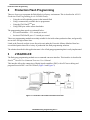
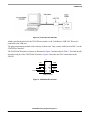
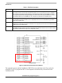
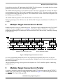
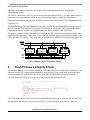
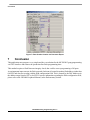
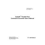
Freescale Semiconductor
Application Note
Document Number: AN3337
Rev. 0, 11/2007
MC56F8013 Gang Programming
by: Paulo Knirsch
RTAC Americas
1
Introduction
This application note describes how to implement a
simple gang programming technique for Freescale's
MC56F8013 devices using the JTAG interface. The
proposed programming method does not verify
programming success in all devices, consequently it is
necessary to include a mechanism for verification. For
this purpose a flash checksum routine was developed in
the application´s start up code. It verifies whether the
flash content is equal to the expected code. The main
objective of gang programming is to reduce the
programming time.
© Freescale Semiconductor, Inc., 2007. All rights reserved.
Contents
1
2
3
4
5
6
7
Introduction . . . . . . . . . . . . . . . . . . . . . . . . . . . . . . . . . . .
Production Flash Programming . . . . . . . . . . . . . . . . . . . .
JTAG/EOnCE . . . . . . . . . . . . . . . . . . . . . . . . . . . . . . . . .
Multiple Target Connection in Series. . . . . . . . . . . . . . . .
Multiple Target Connection in Parallel. . . . . . . . . . . . . . .
Flash Firmware Integrity Check. . . . . . . . . . . . . . . . . . . .
Conclusion. . . . . . . . . . . . . . . . . . . . . . . . . . . . . . . . . . . .
1
2
2
5
6
6
8
Production Flash Programming
2
Production Flash Programming
There are four ways to program the flash blocks in a factory environment. This is described in AN3118
Production Flash Programming for the 56F8000 Family:
• Using the serial bootloader present in the internal flash
• Using a commercially available device programmer
• Using the JTAG/OnCEΤΜ port
• Using GPIO pins with a custom bootloader
The programming data speeds are estimated below:
• SCI serial bootloader = 2.5 k words per second
• In-circuit JTAG/OnCE port = 3 k words per second
These two programming methods are mainly suitable for low/mid volume production lines, and generally
are too slow for high volume lines.
Listed at the Freescale website (www.freescale.com) under the Freescale Alliance Member Portal are
several third parties that offer a variety of production line flash programming solutions.
The solution described in this application note is for a flash gang programming that is easily implemented.
3
JTAG/EOnCE
The flash gang programming method uses a command converter interface. This interface is described in
Suite56TM Parallel Port Command Converter User’s Manual.
This interface allows the connection of digital signal controllers (DSC) with a PC host to debug and
program Freescale DSCs via JTAG/EOnce (Figure 1 and Figure 2).
Figure 1. Connection via Parallel Command Converter
MC56F8013 Gang Programming, Rev. 0
2
Freescale Semiconductor
JTAG/EOnCE
Figure 2. Connection via USB TAP
Another possible hardware for the JTAG/EOnce interface is the CodeWarrior USB TAP. This tool is
connected to the USB port.
The gang programming method works with any of these tools. They connect with Freescale DSCs via the
JTAG/EOnce interface.
The JTAG/EOnCE interface connector is illustrated in Figure 3.and described in Table 1. This table briefly
describes each pin of the JTAG/EOnCE interface. Figure 4 describes the JTAG connections in the
56F8013.
J1
TDI
TDO
TCK
X
RESET
+3.3V O
DE
1
3
5
7
9
11
13
2
4
6
KEY
10
12
14
GND
GND
GND
TMS
X
X TRST
JTAG Connector
Figure 3. JTAG/EOnCE Connector
MC56F8013 Gang Programming, Rev. 0
Freescale Semiconductor
3
JTAG/EOnCE
Table 1. JTAG Pins Description
Pin Name
Pin Description
TCK
Test Clock Input — This input pin provides the clock to synchronize the test logic. It shifts serial data to and
from all TAP controllers and the TLM. If the EOnCE module is not accessed using the master or 56800E core
TAP controllers, the maximum TCK frequency is 1/4 the maximum frequency for the 56800E core. When
accessing the EOnCE module through the 56800E core TAP controller, the maximum frequency for TCK is 1/8
the maximum frequency for the 56800E core. The TCK pin has a pull down non-disabled resistor.
TDI
Test Data Input — This input pin provides a serial input data stream to the TAP and the TLM. It is sampled on
the rising edge of the TCK. The TDI has an on-chip pullup resistor that can be disabled through PUPEN
register in the GPIO module.
TMS
Test Mode Select Input — This input pin is used to sequence the TAP controller’s TLM state machine. It is
sampled on the rising edge of the TCK. The TMS has an on-chip pull-up resistor that can be disabled through
PUPEN register in the GPIO module.
TDO
Test Data Output — This three state output pin provides a serial output data stream from the Master TAP, or
the 56800E core TAP controller. It operates in the Shift-IR and Shift-DR controller states of the TAP controller
state machines. Output data changes on the falling edge of TCK.
JTAG Interface Pins
JTAG Interface Pins
Figure 4. JTAG Pins Connections to the 56F8013
The command converter and the CodeWarrior USB TAP are not stand-alone tools. They need to be
controlled via a PC to program the DSC. In a development environment they can both work with
CodeWarrior IDE.
MC56F8013 Gang Programming, Rev. 0
4
Freescale Semiconductor
Multiple Target Connection in Series
Freescale also provides a PC application called 56800E Flash Programmer. It is suitable for a low volume
production environment as well as in-field firmware upgrades.
The 56800E Flash Programmer is provided in two forms. The first is command-line oriented. This allows
easy integration with scripts. The second is a graphical user interface (GUI). This runs in windows to allow
easy rapid flash loading onto the target device. The command line version is backwards compatible with
the old flash over the JTAG tool.
The 56800E Flash Programmer can be downloaded at www.freescale.com.
Flash programming tool for 56F83xx/1xx and 56F801x DSCs. Requires installation of CodeWarrior 7.2
or higher.
4
Multiple Target Connection in Series
Multiple target devices may be connected in series. This allows a single command converter, JTAG/OnCE
connector to control multiple devices, as in Figure 5. Data flows from the JTAG host to each JTAG
implementation through TDI, out through TDO and back into TDI in the next chip, eventually returning
to the JTAG host.
RESET
TRST
TDO
TRST RESET
TDI
TDO
TCK TMS
TRST RESET
TDO
TDI
TCK TMS
TRST RESET TRST RESET
TDO
TDI
TDO
TDI
TCK TMS
TCK TMS
TRST RESET
TDI
TDO
TCK TMS
TRST RESET
TDO
TDI
TCK TMS
TDI
TCK
TMS
Maximum of 4 Loads on TCK Circuits
Buffer– 74HCT244 or Similar
Figure 5. Multiple Target Connection in Series
In a series programming method, the devices are programmed sequentially; this means, one-by-one.
Consequently, this solution reduces the connecting time. Multiple devices can be connected at the same
time in the programmer.
This programming topology also requires the development of a JTAG controller capable of addressing
multiple devices.
5
Multiple Target Connection in Parallel
A system is developed to make the gang programming simple. This system connects four MC56F8013
with the same JTAG connector according with the schematics in Figure 6. Connected in parallel are the
pins RESET, TCK, TMS, VDD and GND.
MC56F8013 Gang Programming, Rev. 0
Freescale Semiconductor
5
Flash Firmware Integrity Check
The TDI is also connected parallel with the four DSCs, supplying them with the programming
data/command stream.
The TDO is connected to a DSC to avoid a short-circuit with multiple devices. The DSC must always be
connected to the programming circuits. It acts as the feedback supplier to the JTAG programmer.
This makes it possible to gang program four DSCs with the same JTAG interface. The programming time
is around 4.5 s.
The main drawback of this implementation is that only one DSC has its programming success guaranteed:
the DSC with the TDO signal connected to the JTAG interface. All the other DSCs go through a blind
programming process, and the correct programming can not be verified via the JTAG host.
The proposed solution for this drawback is to include in the DSC a flash firmware integrity check at the
beginning of the application. If the check is successful, the firmware signals it to the external world via an
Led or any other user interface. This signal must be verified in the production line together with other tests.
RESET
TRST
TDO
TRST RESET
TDI
TDO
TCK TMS
TRST RESET
TDO
TDI
TCK TMS
TRST RESET
TDO
TDI
TCK TMS
TRST RESET
TDO
TDI
TCK TMS
TDI
TCK
TMS
Figure 6. Multiple Target Connection in Parallel
6
Flash Firmware Integrity Check
The firmware integrity check routine calculates a 32-bit checksum over the whole flash program area. The
firmware verifies if it is equal with the predefined expected value. If the verification succeeds the code
executes normally the applications code. If the check fails, the application execution is blocked.
The code lines below illustrate a simple use of the flash firmware integrity check.
The verify flash integrity routine verifies the flash content after executing the start up code. If it succeeds,
the application initialization code executes normally, as well as the application code. If it fails, the
MC56F8013 Gang Programming, Rev. 0
6
Freescale Semiconductor
Flash Firmware Integrity Check
application code is blocked and the program execution is trapped in an infinite loop. If the COP watchdog
is enabled the DSC resets.
The verify flash integrity routine code is shown below. A pointer (ptr) appears and sweeps all flash
addresses excluding the addresses 0x1FFE and 0x1FFF. These last two specific addresses store the
expected checksum, and are not included in the checksum calculations.
The read program memory is an optimized routine for accessing data in the program flash. It has an input
pointer for specifying the reading address, and as output it returns a word with the data.
Finally, the flash signature routine reads the expected checksum already programmed in flash and returns
it as a double word. Below is the routine code.
The last important point is how to program the expected checksum in specified addresses. This is done via
a linker file edition.
For using processor EXPERT an extra memory section is created as shown in the Figure 7. The address is
where the expected checksum is programmed.
After creating this memory section, the generate linker file option in EXPERT processor is turned off. This
procedure prevents overwriting the changes that are done in the linker file.
The following code is added to the linker file. This code forces the programming of the expected checksum
in the specified section address.
MC56F8013 Gang Programming, Rev. 0
Freescale Semiconductor
7
Conclusion
Figure 7. Extra Section Creation via Processor Expert
7
Conclusion
This application note proposes a very simple and low cost solution for the MC56F8013 gang programming
via JTAG interface and reduces the production line flash programming time.
This method requires a flash firmware integrity check, that verifies correct programming of all parts.
As an important improvement, the flash expected checksum is located in another flash address (other then
0x1FFE) and does not overlap with the flash configuration field. This is located by the DSC hardware in
the address range from 0x1FF7 to 0x1FFF. For more information regarding the flash configuration field,
please refer to the 56F8000 Peripheral Manual, in the flash memory section.
MC56F8013 Gang Programming, Rev. 0
8
Freescale Semiconductor
Conclusion
MC56F8013 Gang Programming, Rev. 0
Freescale Semiconductor
9
How to Reach Us:
Home Page:
www.freescale.com
Web Support:
http://www.freescale.com/support
USA/Europe or Locations Not Listed:
Freescale Semiconductor, Inc.
Technical Information Center, EL516
2100 East Elliot Road
Tempe, Arizona 85284
+1-800-521-6274 or +1-480-768-2130
www.freescale.com/support
Europe, Middle East, and Africa:
Freescale Halbleiter Deutschland GmbH
Technical Information Center
Schatzbogen 7
81829 Muenchen, Germany
+44 1296 380 456 (English)
+46 8 52200080 (English)
+49 89 92103 559 (German)
+33 1 69 35 48 48 (French)
www.freescale.com/support
Japan:
Freescale Semiconductor Japan Ltd.
Headquarters
ARCO Tower 15F
1-8-1, Shimo-Meguro, Meguro-ku,
Tokyo 153-0064
Japan
0120 191014 or +81 3 5437 9125
[email protected]
Asia/Pacific:
Freescale Semiconductor Hong Kong Ltd.
Technical Information Center
2 Dai King Street
Tai Po Industrial Estate
Tai Po, N.T., Hong Kong
+800 2666 8080
[email protected]
For Literature Requests Only:
Freescale Semiconductor Literature Distribution Center
P.O. Box 5405
Denver, Colorado 80217
1-800-441-2447 or 303-675-2140
Fax: 303-675-2150
[email protected]
Document Number: AN3337
Rev. 0
11/2007
Information in this document is provided solely to enable system and software
implementers to use Freescale Semiconductor products. There are no express or
implied copyright licenses granted hereunder to design or fabricate any integrated
circuits or integrated circuits based on the information in this document.
Freescale Semiconductor reserves the right to make changes without further notice to
any products herein. Freescale Semiconductor makes no warranty, representation or
guarantee regarding the suitability of its products for any particular purpose, nor does
Freescale Semiconductor assume any liability arising out of the application or use of any
product or circuit, and specifically disclaims any and all liability, including without
limitation consequential or incidental damages. “Typical” parameters that may be
provided in Freescale Semiconductor data sheets and/or specifications can and do vary
in different applications and actual performance may vary over time. All operating
parameters, including “Typicals”, must be validated for each customer application by
customer’s technical experts. Freescale Semiconductor does not convey any license
under its patent rights nor the rights of others. Freescale Semiconductor products are
not designed, intended, or authorized for use as components in systems intended for
surgical implant into the body, or other applications intended to support or sustain life,
or for any other application in which the failure of the Freescale Semiconductor product
could create a situation where personal injury or death may occur. Should Buyer
purchase or use Freescale Semiconductor products for any such unintended or
unauthorized application, Buyer shall indemnify and hold Freescale Semiconductor and
its officers, employees, subsidiaries, affiliates, and distributors harmless against all
claims, costs, damages, and expenses, and reasonable attorney fees arising out of,
directly or indirectly, any claim of personal injury or death associated with such
unintended or unauthorized use, even if such claim alleges that Freescale
Semiconductor was negligent regarding the design or manufacture of the part.
RoHS-compliant and/or Pb-free versions of Freescale products have the functionality
and electrical characteristics as their non-RoHS-compliant and/or non-Pb-free
counterparts. For further information, see http://www.freescale.com or contact your
Freescale sales representative.
For information on Freescale’s Environmental Products program, go to
http://www.freescale.com/epp.
Freescale™ and the Freescale logo are trademarks of Freescale Semiconductor, Inc.
All other product or service names are the property of their respective owners.
© Freescale Semiconductor, Inc. 2007. All rights reserved.