1
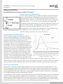
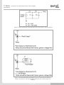
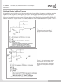
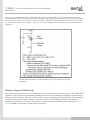
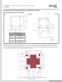
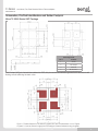
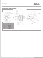
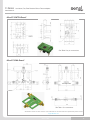
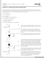
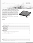
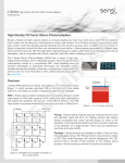
C-Series
Low Noise, Fast, Blue-Sensitive Silicon Photomultipliers
USER MANUAL
C-Series: Low Noise, Fast, Blue-Sensitive Silicon Photomultipliers
SensL’s C-Series low-light sensors feature an industry-leading low dark-count
rate, combined with high PDE and are available with SensL’s proprietary fast mode
output. Three sensor sizes are available; 1mm, 3mm and 6mm packaged in a variety
of formats including TO-can, ceramic header and 4-side tileable surface mount
technology (SMT) package. In addition, two evaluation boards are available with premounted SMT sensors to facilitate rapid product evaluation.
This User Manual covers all aspects of using and understanding the C-Series range
of sensors and evaluation boards. More details on the performance characteristics of
the C-Series sensors can be found in the C-Series datasheet.
Overview
The C-Series SiPM sensors from SensL are based on a P-on-N diode
structure (Figure 1) that results in a high PDE (Photon Detection Efficiency)
and sensitivity into the UV.
C-Series
All C-Series SiPM sensors also feature SensL’s proprietary fast output
terminal (Figure 2), giving access to signals with extremely fast rise times
and short pulse widths.
C-Series SiPM products are available in either MicroSC (2-pin) or MicroFC
(3-pin) versions.
Figure 1, P-on-N sensor structure
MicroSC
Although all C-Series SiPM sensors have the
architecture shown in Figure 2, MicroSC packaged
products only have two pins giving access to the anode
and cathode. The fast output is not accessible in
MicroSC products.
MicroFC
MicroFC packaged products have three (or more) pins,
giving access to the fast output as well as the anode
and cathode. The fast output is the derivative of the
internal fast switching of the microcell in response to the
detection of a single photon.
Figure 2, Simplified microcell level
schematic of the C-Series SiPM.
SensL © 2014
1
C-Series
Low Noise, Fast, Blue-Sensitive Silicon Photomultipliers
USER MANUAL
Contents
Overview...................................................................................................................................................................................................1
MicroSC...............................................................................................................................................................................1
MicroFC...............................................................................................................................................................................1
Glossary....................................................................................................................................................................................................3
Biasing and Readout.................................................................................................................................................................................4
Fast Mode Biasing and Readout of MicroFC Sensors.....................................................................................................................4
Recommended Fast Mode Readout....................................................................................................................................4
Fast Output Amplification.....................................................................................................................................................4
Recommended Fast Mode Biasing......................................................................................................................................4
Standard Mode Biasing and Readout of C-Series Sensors.............................................................................................................6
Recommended Standard Mode Biasing...............................................................................................................................6
Recommended Standard Mode Readout and Amplification.................................................................................................6
Dual Mode Readout of MicroFC Sensors........................................................................................................................................7
Readout of Arrays of SiPM Devices.................................................................................................................................................8
C-Series Mounted Sensors........................................................................................................................................................................9
MicroFC-SMA.................................................................................................................................................................................9
MicroFC-SMTPA.............................................................................................................................................................................10
Schematics, Pin/Pad Identification and Solder Footprint............................................................................................................................11
MicroFC 30000 Series SMT Package.............................................................................................................................................11
Schematics, Pin/Pad Identification and Solder Footprint............................................................................................................................12
MicroFC 60000 Series SMT Package.............................................................................................................................................12
MicroSC 30000 (and 10000) Series X13 Ceramic Package . ..........................................................................................................13
MicroSC 60000 Series X13 Ceramic Package................................................................................................................................13
MicroFC 10000 Series X18 Package...............................................................................................................................................14
MicroFC-SMTPA Board..................................................................................................................................................................15
MicroFC-SMA Board*.....................................................................................................................................................................15
Handling and Soldering.............................................................................................................................................................................16
Safe Handling of Sensors................................................................................................................................................................16
Package Summary.........................................................................................................................................................................16
SMT Package.................................................................................................................................................................................17
X18 Package..................................................................................................................................................................................18
X13 Package..................................................................................................................................................................................18
‘Not Connected’ (NC) Pads and Pins..............................................................................................................................................18
Further Help..............................................................................................................................................................................................19
Appendix A - Alternative Biasing in Fast Mode...........................................................................................................................................20
SensL © 2014
2
C-Series
Low Noise, Fast, Blue-Sensitive Silicon Photomultipliers
USER MANUAL
Glossary
C-Series - A family of SiPM products based upon a P-on-N structure, featuring sensitivity into the UV.
FC - C-Series SiPM product that has at least 3 pins (or pads) accessible that include anode, cathode and the fast
output and can therefore be used in fast mode configuration.
SC - C-Series SiPM product that has only 2-pins accessible, giving access to the anode and cathode. The third
terminal (fast output) is not accessible, and so SC sensors can only work in standard mode.
Fast mode - Using the fast output signal from an FC product for improved timing or photon counting applications.
Standard mode - Using the signal from the anode and cathode for the readout of an SC or FC product where
timing performance is less critical.
SensL © 2014
3
C-Series
Low Noise, Fast, Blue-Sensitive Silicon Photomultipliers
USER MANUAL
Biasing and Readout
Fast Mode Biasing and Readout of MicroFC Sensors
Recommended Fast Mode Biasing
The fast output is referenced to the cathode (substrate) of the SiPM. Therefore
the use of a negative bias voltage applied to the anode with cathode at 0V is
recommended, as in Figure 3. The fast mode signal polarity is positive. (If an
application requires the use of a positive bias, refer to the advice in Appendix A.)
Please refer to the C-Series datasheet for the operating over-voltage range.
The observed signals will be very fast, with rise-times ranging from 300ps to 1ns
and pulse widths of 600ps - 3ns (depending on sensor size). A typical output
pulse for a 3mm sensor (MicroFC-30035) is shown in Figure 4.
Figure 3, Recommended biasing
For all application circuits shown in this User Manual, it is recommended that a
bias voltage filter, such as the one shown in Figure 5, is used.
Alternative biasing schemes are discussed in Appendix A.
Recommended Fast Mode Readout
Due to the extreme speed of the signals from the fast
output, care should be taken in the routing of the signal.
Common microwave/RF design rules, such as controlled
impedance microstrip lines, should be used. The
capacitance of the fast output electrode is much lower (of
the order of 2-3pF for a 1mm device) than in a standard
configuration. The lower output capacitance does not
typically allow the use of a transimpedance amplifier, and
instead one can use an RF style (50W impedance) solution
including direct connection to a coaxial cable. The 3mm
and 6mm devices have higher capacitance, so for best
Figure 4, Fast mode output (red) of a MicroFB-SMA-30035
operation when connecting to an oscilloscope or driving
when illuminated with a 40ps laser pulse (Photek LPG-405).
long wires, it is recommended that the fast output be
~2.5% of microcells are fired in this pulse. Also shown is
connected to an RF transformer such as the RFXF9503 as
part of the standard output pulse, which is shown in full in
in Figure 7. This provides impedance matching, to improve
Figure 9. Scope input = 50W.
amplitude and timing characteristics of the pulse for 50W
impedance. For 1mm devices the capacitance is low enough to allow direct 50W connection as in Figure 6.
Another feature of the fast output electrode is that it is AC-coupled, with no DC component. However, if needed,
one can combine it with the standard output (see the next section) of the SiPM to incorporate DC information.
Fast Output Amplification
It is important to note that the signal charge injected into the fast output electrode is typically about 2% of the
SiPM charge generated during the avalanche. However, the pulse duration is approximately 100 times shorter, so
the current amplitude observed is about 0.02*100 = 2 times higher. This high current amplitude, in combination
with the significantly lower output capacitance, make the device suitable for photon counting at very high speed
(tens of MHz and higher has been demonstrated in the lab).
For amplification of the fast signal it is recommended that a low noise 50W RF amplifier be used. As with standard
readout, the level of gain required is dependent on the application. For applications with high photon counts it is
recommended that the Mini-Circuits ZX60-43S+ be used. For photon counting applications it is recommended
that the Mini-Circuits ZFL-1000LN+ be used. For PET applications it is possible to obtain both timing and energy
resolution information from the fast output, with the anode and cathode only used for biasing.
SensL © 2014
4
C-Series
Low Noise, Fast, Blue-Sensitive Silicon Photomultipliers
USER MANUAL
Figure 5, Generic biasing filter, recommended for all circuits given in this User Manual.
Figure 6, Recommended fast SiPM readout circuitry for 1mm MicroFC sensors.
Figure 7, Recommended fast SiPM readout circuitry for 3mm and 6mm MicroFC
sensors. Also shown is the recommended transformer part number and pin-out
labelling.
SensL © 2014
5
C-Series
Low Noise, Fast, Blue-Sensitive Silicon Photomultipliers
USER MANUAL
Standard Mode Biasing and Readout of C-Series Sensors
For applications that do not require fast timing from the MicroFC, or for the MicroSC products that do not give
access to the fast output signal, SensL’s C-Series sensors will perform as a conventional SiPM. For MicroFC
products the fast output terminal can be left open with no detriment to its standard mode performance. Standard
mode signals may be more suitable for applications involving slow pulses or slowly-varying, continuous light levels,
such as in luminometers or for gamma-ray spectroscopy with slow or low-light scintillators.
Recommended Standard Mode Biasing
Figure 8 below shows the standard mode biasing configuration. For MicroFC sensors the fast output electrode
is left open (unconnected). For all C-Series sensors read out in standard mode, the cathode should be held at a
positive bias with reference to the anode. It is recommended that the signal is taken from the side of the sensor
held at 0V. Reading out in this way yields a pulse that has a rise time of 1ns-10ns and a decay time of several
hundred ns (depending on sensor and microcell size). A typical standard mode output pulse shape is shown in
Figure 9. Alternative biasing schemes are discussed in Appendix A.
Cathode (Open connec)on) Anode Figure 8, Biasing for standard mode. The cathode
should be positive with respect to the anode, but
either a positive or negative bias can be used.
Figure 9, Standard output signal (blue) from a MicroFCSMA-30035 when illuminated with a 40ps laser pulse (Photek
LPG-405). ~2.5% of microcells are fired in this pulse. Also
shown is the fast output (red) from the same pulse. Scope
input = 50W.
When the fast output is not in use it should
be left floating. Do not connect it to ground
or have any wires or cables connected to it.
Recommended Standard Mode Readout and
Amplification
Figure 10 shows how the C-Series devices can be
connected to a standard high speed amplifier, such as
the OPA656, to convert the standard mode output signal
current to a voltage. This technique is recommended for
standard mode readout of all SensL SiPM devices. In the
case of MicroFC devices the fast output can be left open.
Figure 10, Example readout circuit for standard mode.
SensL © 2014
6
C-Series
Low Noise, Fast, Blue-Sensitive Silicon Photomultipliers
USER MANUAL
Dual Mode Readout of MicroFC Sensors
It is possible to read out both fast and standard outputs simultaneously from the sensor to obtain two separate
signals. This can be used for obtaining timing (fast output) and amplitude information (standard output) from
separate channels. This could be useful for applications such as PET (Positron Emission Tomography) where
timing and energy information are required from each photon pulse. Note that this is only possible with MicroFC
sensors. AC and DC coupled options for connecting the device for dual readout are shown in Figures 11 and 12.
Figure 11, DC coupled readout option.
The standard output is amplified
through a transimpedance amplifier
(TIA).
Figure 12, AC coupled readout option.
DC information from the SiPM is lost
but the pulse amplitude is maintained
through the transimpedance amplifier
(TIA).
SensL © 2014
7
C-Series
Low Noise, Fast, Blue-Sensitive Silicon Photomultipliers
USER MANUAL
A third option for simultaneous readout of the standard and fast outputs provides a DC coupled standard output signal,
and preserves the ability to read out the fast output. The decoupling capacitor from the cathode to 0V is critical to provide a
return path for the fast output. This circuit is used on the SensL -SMA and -SMTPA evaluation boards. SensL recommend
the -Vbias readout options from Figures 11 and 12 for most system designs. Alternative biasing schemes are discussed in
Appendix A.
Figure 13, Third option for dual readout that is employed on the SensL -SMA and
-SMTPA evaluation boards. Further information on using a positive bias is given in
Appendix A.
Readout of Arrays of SiPM Devices
Many applications require the use of multiple sensors in the form of an array, such as the SensL Array-SMT line of
products. Large arrays can pose a readout challenge due to the many channels of amplification and processing
that are required. Therefore, methods of reducing the number of channels are often employed in order to reduce
the readout requirements. Many examples of this can be found in the literature, and SensL has extensive
experience in developing solutions for array readout, as demonstrated by the Matrix family of products. A Tech
Note is available on the subject of large area array readout.
SensL © 2014
8
C-Series
Low Noise, Fast, Blue-Sensitive Silicon Photomultipliers
USER MANUAL
C-Series Mounted Sensors
Some C-Series sensors are available ready mounted on test boards, to allow for easy evaluation. The -SMA
and -SMTPA were designed for evaluation of fast output with a DC coupled standard output. The SMA board is
configured for use with the circuit shown in Figure 13 and the SMTPA can also be configured in this way with the
use of an external decoupling capacitor and sense resistor. Note that the 3mm and 6mm versions of the -SMA
and -SMTPA have baluns at their fast outputs for signal shaping and impedance matching. The use of these
boards is detailed in the following sections.
MicroFC-SMA
The MicroFC-SMA-XXXXX product line (Figure 14) features either an SMT or X18 packaged SiPM sensor (type
specified by the XXXXX digits) soldered onto a small PCB board. The board is simple to use, having just three SMA
(female) connectors: one delivers the bias voltage (Vbias) and the other two provide the output signals: standard
output from the anode (Sout) and the fast output (Fout). The circuitry on the board is designed to bias the sensor
in such a way as to retain the optimum high-speed performance. A typical output pulse is shown in Figure 4 which
was taken from a MicroFC-SMA-30035. The circuitry used is as given in Figure 13 with the addition of a bias filter
(Figure 5) and transformer on the fast output of the 3mm and 6mm versions (Figure 7). The schematics showing all
dimensions are on page 16.
Fast
output
Mounting
holes
Bias
SMT
sensor
Standard
output
Figure 14, The MicroFC-SMA board: 3mm SMT version
Output
Vbias
Fout
Sout
Connector
Standard female
SMA connector
Function
bias input (cathode)
Comments
positive bias input
fast output
if unused can be left open
standard output (anode)
if unused can be left open
Table 1, SMA Connections
The MicroFC-SMA is recommended for users who require a plug-and-play set-up to quickly evaluate MicroFC
sensors with optimal timing performance. The board provides outputs which can be connected directly to the
oscilloscope or measurement device. The board also allows the standard output from the anode to be observed
at the same time as the fast output. Table 1 summarizes the connections to the SMA board. Each board has two
mounting holes to allow secure placement during testing, with sensors located at the edge of the board. This
allows two sensors to be placed in close proximity for coincidence timing measurements.
SensL © 2014
9
C-Series
Low Noise, Fast, Blue-Sensitive Silicon Photomultipliers
USER MANUAL
MicroFC-SMTPA
The MicroFC-SMTPA-XXXXX, or Pin Adapter board (Figure 15), features an SMT-packaged SiPM sensor (type
specified by the XXXXX digits) mounted onto a small PCB board. The PCB has five through-hole pins that allow
easy electrical connections to the electrodes of the SMT sensor. The pins are labeled on the PCB with numbers
1 - 5. Each of the numbered pins is connected as listed in Table 2, with the option to use either a positive or
negative bias. Note that the positive bias configuration (see Figure 13) will provide better timing performance than
the negative bias configuration.
Pin
No.
Connection
1
Function
Positive bias
Negative bias
anode
standard output
(if unused connect to zero V)
negative bias input
2
fast
fast output
(if unused can be left open)
fast output
(if unused can be left open)
3
cathode
positive bias input
standard output
(if unused connect to zero V)
4
gnd
PCB gnd
PCB gnd
5
n/c
do not connect
do not connect
Figure 15, Pin numbering on the
MicroFC-SMTPA board
Table 2, Pin assignments for the MicroFC-SMTPA board
The biasing circuit of the SMTPA is the same as on the SMA board (as indicated by Figure 13), however it does
not contain any on-board decoupling on the bias line. Therefore, a bias filter, such as that in Figure 5, should be
included on the bias line before connecting to the relevant bias input pin (see Table 2). The standard output can
be connected directly to an amplifier or 50W load oscilloscope. If the standard output is not used, then that pin
should be connected to zero Volts.
It should be noted that the presence of the pins will slightly degrade the signal from the sensor. Figure 16 shows a
typical pulse from a MicroFC-SMTPA-30035.
The connectors from Samtec used are:
BBL-103-G-E
BBL-102-G-E
Compatible sockets from Samtec are:
SL-103-G-10
SL-102-G-10
Figure 16, Typical pulse from a MicroFCSMTPA-30035
SensL © 2014
10
C-Series
Low Noise, Fast, Blue-Sensitive Silicon Photomultipliers
USER MANUAL
Schematics, Pin/Pad Identification and Solder Footprint
MicroFC 60000 Series SMT Package
5
Pin Assignments
Pin #
C-Series
1
Anode
2
Fast Output
3
Cathode
4
No Connect *
5
No Connect *
* No Contact (NC) pin 4 should be soldered to PCB, this pin can be connected to ground but it can also be left floating without affecting
the dark noise. Recommend that NC pin 5 paddle is not soldered to the PCB and left floating to achieve optimal soldering on pins 1 to 4.
Care must be taken to ensure that no electrical contacts on the PCB, such as vias, short out on the paddle if using the area underneath for
routing. If it is desired to solder pin 5 to the PCB, for example to heatsink or ground the paddle, please consult your contract manufacture
for their solder recommendations based on their equipment and capabilities.
Figure 18, Solder footprint for the MicroFC-600XX-SMT part. All
dimensions in mm.
SensL © 2014
11
C-Series
Low Noise, Fast, Blue-Sensitive Silicon Photomultipliers
USER MANUAL
Schematics, Pin/Pad Identification and Solder Footprint
MicroFC 30000 Series SMT Package
Pin Assignments
Pin #
C-Series
1
Anode
2
Fast Output
3
Cathode
4
No Connect *
* No Contact (NC) pin 4 should be soldered to PCB, this pin can be connected to ground but it can also be left
floating without affecting the dark noise.
Figure 17, Solder footprint for the MicroFC-300XX-SMT part. All dimensions in mm. Fingers
on pads 1-4 can be omitted in tight pitch PCB designs to better facilitate routing of signals.
SensL © 2014
12
C-Series
Low Noise, Fast, Blue-Sensitive Silicon Photomultipliers
USER MANUAL
Schematics, Pin/Pad Identification and Solder Footprint
MicroFC 10000 Series SMT Package
Pin Assignments
Pin #
C-Series
1
Anode
2
Fast Output
3
Cathode
4
No Connect *
* No Contact (NC) pin 4 should be soldered to PCB, this pin can be connected to ground but it can also be left
floating without affecting the dark noise.
Figure 18, Solder footprint for the MicroFC-100XX-SMT part. All
dimensions in mm.
SensL © 2014
13
C-Series
Low Noise, Fast, Blue-Sensitive Silicon Photomultipliers
USER MANUAL
MicroSC 30000 Series X13 Ceramic Package
Pin Assignments
Pin #
C-Series
1
Anode (P)
2
Cathode (N)
MicroSC 60000 Series X13 Ceramic Package
Pin Assignments
Pin #
SensL © 2014
C-Series
1
Anode (P)
2
Cathode (N)
14
C-Series
Low Noise, Fast, Blue-Sensitive Silicon Photomultipliers
USER MANUAL
MicroFC 10000 Series X18 Package
Pin Assignments
Pin #
C-Series
1
Fast Output
2
Cathode (N)
3
GND
4
Anode (P)
SensL © 2014
15
C-Series
Low Noise, Fast, Blue-Sensitive Silicon Photomultipliers
USER MANUAL
MicroFC-SMTPA Board*
See Table 2 for pin connections.
MicroFC-SMA Board*
See Table 1 for connections.
* Schematics shown for 3mm versions. If the schematics for the other sizes are required then please contact
[email protected]
SensL © 2014
16
C-Series
Low Noise, Fast, Blue-Sensitive Silicon Photomultipliers
USER MANUAL
Handling and Soldering
Safe Handling of Sensors
• When unpacking, care should be taken to prevent dropping or misorienting the sensors. The specific items
contained in the package and the type of packaging will depend on the parts ordered.
• Remember that the SiPM is a sensitive optoelectronic instrument; always handle the sensor as carefully as
possible.
• The sensor should be disconnected from the bias supply when not in use.
• SiPM sensors are ESD sensitive. The following precautions are recommended:
• Ensure that personal grounding, environmental controls and work surfaces are compliant with
recommendations in JESD625.
• Ensure that all personnel handling these devices are trained according to the recommendations in
JESD625.
• Devices must be placed in an ESD approved carrier during transport through an uncontrolled area.
Package Summary
Table 3 summarizes packages and product type. In the following sections, handling and soldering advice is given
for each package type.
Package type
Delivery option
code
Product type
MSL*
Reflow Solder?
SMT - Tape & Reel
TR
FC
3
Y
SMT - Cut Tape
TA
FC
4
Y
SMT - Other
WP, GP
FC
N/A
Y**
X18
X13
PK
FC
SC
N/A
N
N/A
N
PK
Table 3, Summary of which package types are associated with which product type.
* See Table 4 for definition
** Sensors shipped in either a waffle pack (WP) or gel pack (GP) require a bake according to J-STD-20,
prior to reflow soldering
SensL © 2014
17
C-Series
Low Noise, Fast, Blue-Sensitive Silicon Photomultipliers
USER MANUAL
SMT Package
A dedicated SMT Handling and Soldering Tech Note is available that contains in depth information on the storage
and use of the SMT parts, including the CAD for the tape and reels.
The SMT package is compatible with standard reflow solder processes (J-STD-20) and so is ideal for high volume
manufacturing. The recommended solder footprints are shown in the Schematics section of this document. If the
SMT part is being assembled into an array, the advice on page 11 and in the SMT Array Tech Note should be
followed.
SMT SiPM sensors are shipped in moisture barrier bags (MBB) according to the J-STD 033 standard. An
unopened MBB should be stored at a temperature below 40OC with humidity below 90%RH. After the MBB has
been opened, the devices must be reflow soldered within a period of time depending on the moisture sensitivity
level (MSL). SensL SMT Tape & Reel are MSL 3, cut tape SMT are MSL 4 and SMT sensors shipped in trays
require a bake prior to reflow soldering. See Table 4 for details.
MSL
Exposure time
Condition
3
4
168 hours
72 hours
≤30 °C/60% RH
≤30 °C/60% RH
Applicable SMT
shipping format
Tape and reel
Cut tape and partial
reels
Table 4, MSL definitions applicable to SensL products (reference J-STD 020).
All SMT shipped on tray do not have an MSL rating and should be baked prior to placement on PCB.
Please discuss this with your contract manufacture for their recommended baking cycle which adheres
to IPC/JEDEC J-STD-20 MSL Classification. Note the temperature of the bake should not exceed the
recommended operating temperature of the product listed in product’s datasheet.
Exposure to solvents such as concentrated isopropyl alcohol (propan-2-ol) or commercial flux removal fluids such
as Fluxene will cause severe, irreversible damage to the MLP packages. If cleaning is necessary, a 20% solution of
isopropyl alcohol can be used. Futher details on cleaning can be found in the SMT Handling Guide.
Creating Arrays of SMT Sensors
If multiple SMT parts are to be mounted in close proximity (e.g. 1D or 2D arrays), the following recommendations
may be helpful. By following this recommendations, a planarity of 0.09% to 0.53% can be achieved.
• Minimum spacing between SMT parts of 200mm.
• Use of FR4 PCB as the substrate material
• Use commercial automatic placement machines to achieve the necessary placement accuracy to
give the above spacing and planarity.
• Take into account the MSL 3 specifications of the SMT devices when assembling.
• Hold the PCB board in a rigid frame to avoid warping due to the heat process.
• The user can refer to the additional Tech Note on this subject.
SensL © 2014
18
C-Series
Low Noise, Fast, Blue-Sensitive Silicon Photomultipliers
USER MANUAL
X18 Package
The X18 (TO-18 can) package has through-hole pins and hand-soldering is recommended. The SiPM can be
damaged by excessive heat and so it is important that due care be given to temperature and dwell time when
soldering the X18 products. A maximum temperature of 260oC for no more than 10 seconds is recommended.
More details can be found in the Hand Soldering Guide Tech Note.
X13 Package
The X13 ceramic package has through-hole pins and hand-soldering is recommended. The SiPM can be
damaged by excessive heat and so it is important that due care be given to temperature and dwell time when
soldering the X13 products. A maximum temperature of 260oC for no more than 5 seconds, applied at a
distance of 2mm from the ceramic base is recommended. More details can be found in the Hand Soldering
Guide Tech Note.
‘Not Connected’ (NC) Pads and Pins
Common PCB design practice is to ground any floating pins or pads such as those labelled ‘NC’. Grounding the
pin helps shielding and can reduce noise interference from external sources (EMI/RF).
SensL © 2014
19
C-Series
Low Noise, Fast, Blue-Sensitive Silicon Photomultipliers
USER MANUAL
Further Help
If more help is required in the set-up or operation of C-Series sensors, there are several SensL resources that can
help.
• The C-Series Datasheet contains more detailed information on the physical and performance characteristics of
the sensors.
• A variety of Tech Notes are available on the website, www.sensl.com, such as:
• A guide to handling and soldering SMT packages.
• A guide to hand soldering through-hole SensL sensor products.
• A guide on creating arrays of close-packed SMT sensors.
• An extensive library of technical and scientific papers on the use of SensL SiPM sensors.
• If additional help is needed, please contact [email protected]
SensL © 2014
20
C-Series
Low Noise, Fast, Blue-Sensitive Silicon Photomultipliers
USER MANUAL
Appendix A - Biasing Alternatives & Signal Polarity
This Appendix lists all of the possible ways in which a C-Series SiPM can be biased. Not all of them will deliver
optimimum performance but are included for completeness. For each biasing arrangement, the standard and fast
signal polarities are given. The following abbreviations are used throughout:
Vbias = bias voltage
Sout = standard output
Fout = fast output
Rs = load resistor for the standard output
Rf = load resistor for the fast output
Vs = standard output voltage
Vf = fast output voltage
RQ = quench resistor (included on the SiPM die)
A
When using one of the MicroFC products in fast mode, it is
recommended to use biasing scheme A, as shown on the
left.
This configuration will give the best timing performance
and if fast output only is required then the resistor Rs can
be zero ohms or -Vbias can be applied directly to the SiPM
cathode.
Note that there will be a negative offset on the Sout signal
in this configuration as the pulse is referenced to -Vbias.
B
A positive bias can be applied to the cathode (substrate), as
shown in B on the left, without any change in performance.
However, care must be taken to ensure good decoupling
of the bias voltage at the device since the substrate is the
return path for the fast signal. If this biasing configuration is
required, it is recommended that a 10nF (50V) ceramic SMT
decoupling capacitor with low ESR is placed as close to the
cathode as possible.
Without suitable decoupling the fast output pulse can suffer
from ringing and pulse shape distortion when the positively
biased cathode configuration is used.
An advantage of this configuration over configuration A is
that the standard output is now referenced to 0V potential.
However if the standard output is not required then the
resistor Rs can again be made zero ohms or the SiPM
anode connected directly to 0V.
SensL © 2014
21
C-Series Low Noise, Fast, Blue-Sensitive Silicon Photomultipliers
USER MANUAL
C
D
Neither of the biasing schemes represented in C or D are recommended for use with high precision timing
applications on the standard or in particular the fast output as these schemes would require the cathode substrate
plane of the SiPM chip to be switched. However, either would be suitable for applications where the pulse timing is
not critical.
www.sensl.com
[email protected]
+353 21 240 7110 (International)
+1 650 641 3278 (North America)
All specifications are subject to change without notice
Rev. 1.6, October 2015
SensL
SensL©©2014
2014
22