1
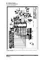
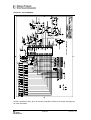
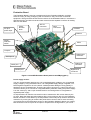
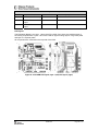
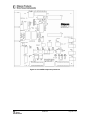
High-frequency
crystal
Trimmer
capacitor
32.768 kHz
crystal
Power
connections
Antenna
connector
CC1010
Temperature
sensor
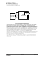
Figure 1: CC1010EM Evaluation Module
PCB layout
The figure above shows the 1.0 revision of the PCB. Later revisions are similar, but have the
following additional features:
•
0-ohm series resistor between the temperature sensor and the AD1 bit of CC1010.
Instead of desoldering the temperature sensor if you wish to use AD1 for other
purposes, you can desolder the 0-ohm resistor.
•
0-ohm series resistor between temperature sensor and VDD. Instead of desoldering
the temperature sensor when measuring the power-down current of the CC1010, you
can desolder the 0-ohm resistor.
RF circuits operating at high frequencies are sensitive to the physical layout of the PCB.
Chipcon has carefully optimized the layout of the CC1010EM evaluation module, and we
recommend that you copy it when making your own PCB design.
The PCB is of a 4-layer type in order to provide a good ground plane as well as adequate
routing space. The laminate used is standard FR-4 board material. The PCB is 1.6mm thick,
with layer 1 on the top side, layers 2 and 3 are internal layers and layer 4 is on the bottom
side. Layers 1 and 4 are used for routing, while layer 2 is a ground plane and layer 3 is used
for power routing. All areas not utilized for routing are filled with copper connected to ground
to provide RF shielding. The ground planes on all layers are stitched together with closely
spaced vias.
To minimize LO leakage and allow space for decoupling capacitors close to the CC1010, the
VCO inductor (L101) is placed on the bottom side of the PCB. EMI beads for power-supply
filtering are also placed on the bottom side, together with the pull-up resistors. All other
components are placed on the top side of the PCB.
SWRU055
Page 5 of 40