1
USB4CH User Manual
Manual Revision (2010/06/01)
Board Revision E
Symmetric Research
www.symres.com
FREE WEB VERSION - PARTIAL CIRCUIT DIAGRAMS
Contents
1 Introduction
8
2 Getting started
2.1
Find your CDROM . . . . . . . . . .
2.2
Downloading software from the web
2.3
Linux revs . . . . . . . . . . . . . . .
2.4
Hook up power . . . . . . . . . . . .
2.5
Hook up the USB cable . . . . . . .
2.6
Run Diag . . . . . . . . . . . . . . .
2.7
Run DVM or Scope . . . . . . . . .
2.8
Linux USB port permissions . . . . .
.
.
.
.
.
.
.
.
.
.
.
.
.
.
.
.
.
.
.
.
.
.
.
.
.
.
.
.
.
.
.
.
.
.
.
.
.
.
.
.
.
.
.
.
.
.
.
.
.
.
.
.
.
.
.
.
.
.
.
.
.
.
.
.
.
.
.
.
.
.
.
.
.
.
.
.
.
.
.
.
.
.
.
.
.
.
.
.
.
.
.
.
.
.
.
.
.
.
.
.
.
.
.
.
.
.
.
.
.
.
.
.
.
.
.
.
.
.
.
.
.
.
.
.
.
.
.
.
.
.
.
.
.
.
.
.
.
.
.
.
.
.
.
.
.
.
.
.
.
.
.
.
.
.
.
.
.
.
.
.
.
.
.
.
.
.
.
.
.
.
.
.
.
.
.
.
10
10
11
11
11
12
14
14
14
3 Application Programs
3.1
DVM . . . . . . . . . . . . . . . . .
3.1.1 starting the program . . .
3.1.2 ini syntax . . . . . . . . .
3.1.3 GUI version . . . . . . . .
3.1.4 command line version . . .
3.1.5 ASC file format . . . . . .
3.1.6 Calibrate . . . . . . . . . .
3.2
Scope . . . . . . . . . . . . . . . . .
3.2.1 starting the program . . .
3.2.2 ini syntax . . . . . . . . .
3.2.3 GUI version . . . . . . . .
3.2.4 command line version . . .
3.2.5 output file names . . . . .
3.2.6 DAT file format . . . . . .
3.3
Blast . . . . . . . . . . . . . . . . . .
3.3.1 starting the program . . .
3.3.2 output file names . . . . .
3.3.3 PAK file format . . . . . .
3.3.4 typical post processing . .
3.3.5 running in the background
.
.
.
.
.
.
.
.
.
.
.
.
.
.
.
.
.
.
.
.
.
.
.
.
.
.
.
.
.
.
.
.
.
.
.
.
.
.
.
.
.
.
.
.
.
.
.
.
.
.
.
.
.
.
.
.
.
.
.
.
.
.
.
.
.
.
.
.
.
.
.
.
.
.
.
.
.
.
.
.
.
.
.
.
.
.
.
.
.
.
.
.
.
.
.
.
.
.
.
.
.
.
.
.
.
.
.
.
.
.
.
.
.
.
.
.
.
.
.
.
.
.
.
.
.
.
.
.
.
.
.
.
.
.
.
.
.
.
.
.
.
.
.
.
.
.
.
.
.
.
.
.
.
.
.
.
.
.
.
.
.
.
.
.
.
.
.
.
.
.
.
.
.
.
.
.
.
.
.
.
.
.
.
.
.
.
.
.
.
.
.
.
.
.
.
.
.
.
.
.
.
.
.
.
.
.
.
.
.
.
.
.
.
.
.
.
.
.
.
.
.
.
.
.
.
.
.
.
.
.
.
.
.
.
.
.
.
.
.
.
.
.
.
.
.
.
.
.
.
.
.
.
.
.
.
.
.
.
.
.
.
.
.
.
.
.
.
.
.
.
.
.
.
.
.
.
.
.
.
.
.
.
.
.
.
.
.
.
.
.
.
.
.
.
.
.
.
.
.
.
.
.
.
.
.
.
.
.
.
.
.
.
.
.
.
.
.
.
.
.
.
.
.
.
.
.
.
.
.
.
.
.
.
.
.
.
.
.
.
.
.
.
.
.
.
.
.
.
.
.
.
.
.
.
.
.
.
.
.
.
.
.
.
.
.
.
.
.
.
.
.
.
.
.
.
.
.
.
.
.
.
.
.
.
.
.
.
.
.
.
.
.
.
.
.
.
.
.
.
.
.
.
.
.
.
.
.
.
.
.
.
.
.
.
.
.
.
.
.
.
.
.
.
.
.
.
.
.
.
.
.
.
.
.
.
.
.
.
.
.
16
17
18
19
20
21
22
23
25
26
27
28
29
30
31
32
33
36
37
38
39
2
4 Utilities and Format Conversion
4.1
Diag . . . . . . . . . . . . . . .
4.2
DevMan . . . . . . . . . . . . .
4.3
Dat2Asc . . . . . . . . . . . . .
4.4
Pak2Asc . . . . . . . . . . . . .
4.5
Interpolate . . . . . . . . . . .
4.6
View . . . . . . . . . . . . . . .
4.7
NmeaTime . . . . . . . . . . .
4.8
GpsProg . . . . . . . . . . . . .
4.9
DigitalIo . . . . . . . . . . . . .
4.10 SetDid . . . . . . . . . . . . . .
.
.
.
.
.
.
.
.
.
.
40
41
43
44
46
48
49
50
52
53
54
.
.
.
.
.
.
.
.
.
.
.
56
57
61
62
63
65
68
69
70
71
72
73
6 Sampling rates
6.1
Permitted rates . . . . . . . . . . . . . . . . . . . . . . . . . . . . . . . . . .
6.2
Master clock stability . . . . . . . . . . . . . . . . . . . . . . . . . . . . . .
6.3
Interpolation to other sampling rates . . . . . . . . . . . . . . . . . . . . . .
74
75
76
77
7 FIFO Depth and Overflow
7.1
FIFO Depth . . . . . . . . . . . . . . . . . . . . . . . . . . . . . . . . . . .
7.2
FIFO Overflow . . . . . . . . . . . . . . . . . . . . . . . . . . . . . . . . . .
7.3
FIFO Creep . . . . . . . . . . . . . . . . . . . . . . . . . . . . . . . . . . . .
78
78
80
80
8 A/D reference voltage
8.1
Standard reference . . . . . . . . . . . . . . . . . . . . . . . . . . . . . . . .
8.2
Alternate references . . . . . . . . . . . . . . . . . . . . . . . . . . . . . . .
8.3
TC correction with on board temp sensor . . . . . . . . . . . . . . . . . . .
81
82
82
83
9 Analog inputs
9.1
Differential signals . .
9.2
DB15 pin assignments
9.3
Twisted pair cabling .
9.4
Static shielding . . . .
84
84
88
90
91
.
.
.
.
.
.
.
.
.
.
5 User C Library
5.1
Open . . . . . . . . . . . . . . .
5.2
SPS rate table lookup . . . . . .
5.3
Start acquisition . . . . . . . . .
5.4
Get Data as Packets . . . . . . .
5.5
Convert Packets to Columns . .
5.6
User digital IO read . . . . . . .
5.7
User digital IO write . . . . . . .
5.8
Front panel red and yellow LEDs
5.9
Power good . . . . . . . . . . . .
5.10 Stop acquisition . . . . . . . . .
5.11 Close . . . . . . . . . . . . . . . .
.
.
.
.
.
.
.
.
.
.
.
.
.
.
.
.
.
.
.
.
.
.
.
.
.
.
.
.
.
.
.
.
.
.
.
.
.
.
.
.
.
.
.
.
.
.
.
.
.
.
.
.
.
.
.
.
.
.
.
.
.
.
.
.
.
.
.
.
.
.
.
.
.
.
3
.
.
.
.
.
.
.
.
.
.
.
.
.
.
.
.
.
.
.
.
.
.
.
.
.
.
.
.
.
.
.
.
.
.
.
.
.
.
.
.
.
.
.
.
.
.
.
.
.
.
.
.
.
.
.
.
.
.
.
.
.
.
.
.
.
.
.
.
.
.
.
.
.
.
.
.
.
.
.
.
.
.
.
.
.
.
.
.
.
.
.
.
.
.
.
.
.
.
.
.
.
.
.
.
.
.
.
.
.
.
.
.
.
.
.
.
.
.
.
.
.
.
.
.
.
.
.
.
.
.
.
.
.
.
.
.
.
.
.
.
.
.
.
.
.
.
.
.
.
.
.
.
.
.
.
.
.
.
.
.
.
.
.
.
.
.
.
.
.
.
.
.
.
.
.
.
.
.
.
.
.
.
.
.
.
.
.
.
.
.
.
.
.
.
.
.
.
.
.
.
.
.
.
.
.
.
.
.
.
.
.
.
.
.
.
.
.
.
.
.
.
.
.
.
.
.
.
.
.
.
.
.
.
.
.
.
.
.
.
.
.
.
.
.
.
.
.
.
.
.
.
.
.
.
.
.
.
.
.
.
.
.
.
.
.
.
.
.
.
.
.
.
.
.
.
.
.
.
.
.
.
.
.
.
.
.
.
.
.
.
.
.
.
.
.
.
.
.
.
.
.
.
.
.
.
.
.
.
.
.
.
.
.
.
.
.
.
.
.
.
.
.
.
.
.
.
.
.
.
.
.
.
.
.
.
.
.
.
.
.
.
.
.
.
.
.
.
.
.
.
.
.
.
.
.
.
.
.
.
.
.
.
.
.
.
.
.
.
.
.
.
.
.
.
.
.
.
.
.
.
.
.
.
.
.
.
.
.
.
.
.
.
.
.
.
.
.
.
.
.
.
.
.
.
.
.
.
.
.
.
.
.
.
.
.
.
.
.
.
.
.
.
.
.
.
.
.
.
.
.
.
.
.
.
.
.
.
.
.
.
.
.
.
.
.
.
.
.
.
.
.
.
.
.
.
.
.
.
.
.
.
.
.
.
.
.
.
.
.
.
.
.
.
.
.
.
.
.
.
.
.
.
.
.
.
.
.
.
.
.
.
.
.
.
.
.
.
.
.
.
.
.
.
.
.
.
.
.
.
.
.
.
.
.
.
.
.
.
.
.
.
.
.
.
.
.
.
.
.
9.5
9.6
9.7
9.8
Input impedance . .
Input voltage range
Op amp gain . . . .
RC antialias filtering
.
.
.
.
.
.
.
.
.
.
.
.
.
.
.
.
.
.
.
.
.
.
.
.
.
.
.
.
.
.
.
.
.
.
.
.
.
.
.
.
.
.
.
.
.
.
.
.
.
.
.
.
.
.
.
.
.
.
.
.
.
.
.
.
.
.
.
.
.
.
.
.
.
.
.
.
.
.
.
.
.
.
.
.
.
.
.
.
.
.
.
.
.
.
.
.
.
.
.
.
.
.
.
.
.
.
.
.
.
.
.
.
.
.
.
.
.
.
.
.
.
.
.
.
92
93
93
94
10 Analog DC calibration
10.1 Full Scale Voltage Span and Counts . . . . . . . . . . . . . . . . . . . . . .
10.2 Approximate counts per volt . . . . . . . . . . . . . . . . . . . . . . . . . .
10.3 Calibration slope and offset . . . . . . . . . . . . . . . . . . . . . . . . . . .
95
96
97
98
11 Analog AC calibration
100
11.1 Theoretical AC transfer function . . . . . . . . . . . . . . . . . . . . . . . . 101
11.2 Measured transfer function . . . . . . . . . . . . . . . . . . . . . . . . . . . 102
12 Digital IO
12.1 Digital input . . . . . . . . . . . . . . . . . . . . .
12.2 Digital output . . . . . . . . . . . . . . . . . . . .
12.3 Additional digital timing and GPS signals . . . . .
12.4 DB25 pin assignments . . . . . . . . . . . . . . . .
12.5 Static shielding . . . . . . . . . . . . . . . . . . . .
12.6 User configuration byte . . . . . . . . . . . . . . .
12.7 Triggering . . . . . . . . . . . . . . . . . . . . . . .
12.8 Programming the front panel red and yellow LEDs
12.9 Seeing the digital inputs in Scope . . . . . . . . . .
.
.
.
.
.
.
.
.
.
.
.
.
.
.
.
.
.
.
.
.
.
.
.
.
.
.
.
.
.
.
.
.
.
.
.
.
.
.
.
.
.
.
.
.
.
.
.
.
.
.
.
.
.
.
.
.
.
.
.
.
.
.
.
.
.
.
.
.
.
.
.
.
.
.
.
.
.
.
.
.
.
.
.
.
.
.
.
.
.
.
.
.
.
.
.
.
.
.
.
.
.
.
.
.
.
.
.
.
.
.
.
.
.
.
.
.
.
.
.
.
.
.
.
.
.
.
103
103
104
104
105
107
107
108
108
108
13 GPS Time Stamping
13.1 What is GPS ? . . . . . . . . . . . . . . . . . . . .
13.2 Required GPS signals . . . . . . . . . . . . . . . .
13.3 DB25 pin assignments . . . . . . . . . . . . . . . .
13.4 Using a Garmin 16x HVS with the USBxCH . . .
13.5 Determining RS232 polarity . . . . . . . . . . . . .
13.6 Determining PPS polarity . . . . . . . . . . . . . .
13.7 Front panel red LED . . . . . . . . . . . . . . . . .
13.8 Expected NMEA strings . . . . . . . . . . . . . . .
13.9 Programming the GPS antenna . . . . . . . . . . .
13.10 Seeing the GPS time stamps in Scope and Blast .
13.11 What does time stamping mean ? . . . . . . . . .
13.12 Driving multiple USBxCH systems from one GPS
.
.
.
.
.
.
.
.
.
.
.
.
.
.
.
.
.
.
.
.
.
.
.
.
.
.
.
.
.
.
.
.
.
.
.
.
.
.
.
.
.
.
.
.
.
.
.
.
.
.
.
.
.
.
.
.
.
.
.
.
.
.
.
.
.
.
.
.
.
.
.
.
.
.
.
.
.
.
.
.
.
.
.
.
.
.
.
.
.
.
.
.
.
.
.
.
.
.
.
.
.
.
.
.
.
.
.
.
.
.
.
.
.
.
.
.
.
.
.
.
.
.
.
.
.
.
.
.
.
.
.
.
.
.
.
.
.
.
.
.
.
.
.
.
.
.
.
.
.
.
.
.
.
.
.
.
.
.
.
.
.
.
.
.
.
.
.
.
109
109
110
110
112
113
115
116
116
117
118
119
120
14 NTP Time Stamping
121
14.1 Synchronizing the PC clock to NTP . . . . . . . . . . . . . . . . . . . . . . 121
14.2 Setting the USBxCH to use the PC clock . . . . . . . . . . . . . . . . . . . 122
4
15 Power Supply
15.1 Connectors . . . . . . . . . . . .
15.2 Voltage and current requirements
15.3 LED power status indicators . .
15.4 POWER GOOD signal . . . . .
15.5 Reset and power cycling . . . . .
15.6 Current limiting . . . . . . . . .
.
.
.
.
.
.
.
.
.
.
.
.
.
.
.
.
.
.
.
.
.
.
.
.
.
.
.
.
.
.
.
.
.
.
.
.
.
.
.
.
.
.
.
.
.
.
.
.
.
.
.
.
.
.
.
.
.
.
.
.
.
.
.
.
.
.
.
.
.
.
.
.
.
.
.
.
.
.
.
.
.
.
.
.
.
.
.
.
.
.
.
.
.
.
.
.
.
.
.
.
.
.
.
.
.
.
.
.
.
.
.
.
.
.
.
.
.
.
.
.
.
.
.
.
.
.
.
.
.
.
.
.
.
.
.
.
.
.
.
.
.
.
.
.
123
123
124
125
125
126
126
16 Temp Sensor
127
16.1 Temp records . . . . . . . . . . . . . . . . . . . . . . . . . . . . . . . . . . . 127
16.2 System level TC calibration . . . . . . . . . . . . . . . . . . . . . . . . . . . 128
17 Specifications
129
17.1 Specifications table . . . . . . . . . . . . . . . . . . . . . . . . . . . . . . . . 130
17.2 Noise floor . . . . . . . . . . . . . . . . . . . . . . . . . . . . . . . . . . . . . 131
17.3 Thermal response . . . . . . . . . . . . . . . . . . . . . . . . . . . . . . . . . 134
18 Circuit Diagrams
135
19 Examples and Experiments
19.1 Measuring a AA battery . . . . . . . . . .
19.2 Twisted pair for 50/60Hz rejection . . . .
19.3 Absolute calibration . . . . . . . . . . . .
19.4 Using DVM with a 10 turn potentiometer
19.5 Ratiometric technique . . . . . . . . . . .
19.6 Measuring light levels with a solar cell . .
19.7 Plotting results with GnuPlot . . . . . . .
19.8 Passive geophones . . . . . . . . . . . . .
19.9 Multiple USBxCH and network processing
19.10 Powering with batteries . . . . . . . . . .
141
142
147
148
149
154
155
156
159
160
161
.
.
.
.
.
.
.
.
.
.
.
.
.
.
.
.
.
.
.
.
.
.
.
.
.
.
.
.
.
.
.
.
.
.
.
.
.
.
.
.
.
.
.
.
.
.
.
.
.
.
.
.
.
.
.
.
.
.
.
.
.
.
.
.
.
.
.
.
.
.
.
.
.
.
.
.
.
.
.
.
.
.
.
.
.
.
.
.
.
.
.
.
.
.
.
.
.
.
.
.
.
.
.
.
.
.
.
.
.
.
.
.
.
.
.
.
.
.
.
.
.
.
.
.
.
.
.
.
.
.
.
.
.
.
.
.
.
.
.
.
.
.
.
.
.
.
.
.
.
.
.
.
.
.
.
.
.
.
.
.
.
.
.
.
.
.
.
.
.
.
.
.
.
.
.
.
.
.
.
.
.
.
.
.
.
.
.
.
.
.
20 Frequently Asked Questions
166
20.1 Software . . . . . . . . . . . . . . . . . . . . . . . . . . . . . . . . . . . . . . 166
20.2 Hardware . . . . . . . . . . . . . . . . . . . . . . . . . . . . . . . . . . . . . 168
21 Extra supplies
172
21.1 Small Parts for cables etc . . . . . . . . . . . . . . . . . . . . . . . . . . . . 173
22 Using Adobe PDF effectively
176
23 Getting Technical Help
177
5
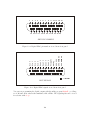
List of Figures
1.1
mini Netbook with USB4CH and geophone . . . . . . . . . . . . . . . . . . .
3.1
3.2
3.3
3.4
3.5
3.6
3.7
3.8
3.9
DVM sample display . .
DVM GUI screen . . . .
DVM CMD text screen
DVM Calibrate screen .
Scope sample display . .
Scope GUI screen . . . .
Scope CMD screen . . .
Blast sample display . .
Blast text screen . . . .
.
.
.
.
.
.
.
.
.
17
20
21
23
25
28
29
32
35
6.1
SPS rate table . . . . . . . . . . . . . . . . . . . . . . . . . . . . . . . . . . .
75
7.1
FIFO hold out time table . . . . . . . . . . . . . . . . . . . . . . . . . . . . .
79
9.1
9.2
9.3
9.4
9.5
9.6
9.7
Differential vs single ended signals . . . . . . . . .
Balanced differential inputs . . . . . . . . . . . . .
Two terminal floating sensor connection . . . . . .
Analog DB15 pin assignment table . . . . . . . . .
Analog DB15 pin numbers viewed from front panel
Analog DB15 pin signals viewed from front panel .
Magnetic coupling of 50/60Hz noise . . . . . . . .
.
.
.
.
.
.
.
85
86
87
88
89
89
90
10.1
10.2
10.3
A/D counts with balanced differential input . . . . . . . . . . . . . . . . . . .
A/D counts with single ended input . . . . . . . . . . . . . . . . . . . . . . .
Production input offset spreads . . . . . . . . . . . . . . . . . . . . . . . . . .
96
97
99
11.1
11.2
AC response: theoretical sinc . . . . . . . . . . . . . . . . . . . . . . . . . . . 101
AC response: physical measurement setup . . . . . . . . . . . . . . . . . . . . 102
12.1
12.2
12.3
12.4
Digital
Digital
Digital
Digital
DB25
DB25
DB25
DB25
.
.
.
.
.
.
.
.
.
.
.
.
.
.
.
.
.
.
.
.
.
.
.
.
.
.
.
.
.
.
.
.
.
.
.
.
.
.
.
.
.
.
.
.
.
.
.
.
.
.
.
.
.
.
.
.
.
.
.
.
.
.
.
.
.
.
.
.
.
.
.
.
.
.
.
.
.
.
.
.
.
.
.
.
.
.
.
.
.
.
.
.
.
.
.
.
.
.
.
.
.
.
.
.
.
.
.
.
.
.
.
.
.
.
.
.
.
.
.
.
.
.
.
.
.
.
.
.
.
.
.
.
.
.
.
pin assignment table . . . . . . . . .
pin numbers viewed from front panel
pin signals viewed from front panel .
UserCfgByte . . . . . . . . . . . . . .
6
.
.
.
.
.
.
.
.
.
.
.
.
.
.
.
.
.
.
.
.
.
.
.
.
.
.
.
.
.
.
.
.
.
.
.
.
.
.
.
.
.
.
.
.
.
.
.
.
.
.
.
.
.
.
.
.
.
.
.
.
.
.
.
.
.
.
.
.
.
.
.
.
.
.
.
.
.
.
.
.
.
.
.
.
.
.
.
.
.
.
.
.
.
.
.
.
.
.
.
.
.
.
.
.
.
.
.
.
.
.
.
.
.
.
.
.
.
.
.
.
.
.
.
.
.
.
.
.
.
.
.
.
.
.
.
.
.
.
.
.
.
.
.
.
.
.
.
.
.
.
.
.
.
.
.
.
.
.
.
.
.
.
.
.
.
.
.
.
.
.
.
.
.
.
.
.
.
.
.
.
.
.
.
.
.
.
.
.
.
.
.
.
.
.
.
.
.
.
.
.
.
.
.
.
.
.
.
.
.
.
.
.
.
.
.
.
.
.
.
.
.
.
.
.
.
.
.
.
.
.
.
.
.
.
.
.
.
.
.
.
.
.
.
.
.
.
.
.
.
.
.
.
.
.
.
.
.
.
.
.
.
.
.
.
.
.
.
.
.
.
.
.
.
.
.
.
.
.
.
.
.
.
.
.
9
105
106
106
107
13.1
13.2
13.3
13.4
13.5
13.6
GPS DB25 pin assignment table . . . .
GPS DB25 pin signals viewed from front
Garmin GPS 16x HVS wires . . . . . . .
Garmin GPS 16x HVS wiring . . . . . .
Garmin GPS 16x HVS finished cabling .
PPS signal polarities . . . . . . . . . . .
. . . .
panel
. . . .
. . . .
. . . .
. . . .
.
.
.
.
.
.
.
.
.
.
.
.
.
.
.
.
.
.
.
.
.
.
.
.
.
.
.
.
.
.
.
.
.
.
.
.
.
.
.
.
.
.
.
.
.
.
.
.
.
.
.
.
.
.
.
.
.
.
.
.
.
.
.
.
.
.
.
.
.
.
.
.
.
.
.
.
.
.
.
.
.
.
.
.
.
.
.
.
.
.
.
.
.
.
.
.
.
.
.
.
.
.
111
111
112
113
114
115
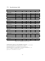
17.1
17.2
17.3
17.4
17.5
Specifications table . . . . . . . .
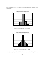
Noise floor time domain plots . .
Noise floor histogram at 130Hz .
Noise floor histogram at 1302Hz
Long term thermal response . . .
.
.
.
.
.
.
.
.
.
.
.
.
.
.
.
.
.
.
.
.
.
.
.
.
.
.
.
.
.
.
.
.
.
.
.
.
.
.
.
.
.
.
.
.
.
.
.
.
.
.
.
.
.
.
.
.
.
.
.
.
.
.
.
.
.
.
.
.
.
.
.
.
.
.
.
.
.
.
.
.
.
.
.
.
.
.
.
.
.
.
.
.
.
.
.
.
.
.
.
.
.
.
.
.
.
.
.
.
.
.
.
.
.
.
.
130
131
132
132
134
19.1
19.2
19.3
19.4
19.5
19.6
19.7
19.8
19.9
19.10
19.11
19.12
19.13
19.14
19.15
19.16
19.17
19.18
AA battery test lead setup . . . . . .
AA battery DVM display screen . . .
AA battery circuit floating . . . . . . .
AA battery with AGND connection .
AA battery circuit grounded . . . . . .
AA battery 6 volt circuit . . . . . . . .
10 turn circuit . . . . . . . . . . . . .
10 turn photo top . . . . . . . . . . . .
10 turn photo bottom . . . . . . . . .
10 turn Calibrate screen . . . . . . . .
10 turn DVM display screen . . . . . .
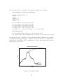
Solar cell light level measurements . .
GnuPlot graph . . . . . . . . . . . . .
NiMH AA battery pack . . . . . . . .
Battery voltage divider . . . . . . . . .
NiMH AA battery pack discharge plot
Lead acid 3Ah battery . . . . . . . . .
Lead acid 3Ah battery discharge plot .
.
.
.
.
.
.
.
.
.
.
.
.
.
.
.
.
.
.
.
.
.
.
.
.
.
.
.
.
.
.
.
.
.
.
.
.
.
.
.
.
.
.
.
.
.
.
.
.
.
.
.
.
.
.
.
.
.
.
.
.
.
.
.
.
.
.
.
.
.
.
.
.
.
.
.
.
.
.
.
.
.
.
.
.
.
.
.
.
.
.
.
.
.
.
.
.
.
.
.
.
.
.
.
.
.
.
.
.
.
.
.
.
.
.
.
.
.
.
.
.
.
.
.
.
.
.
.
.
.
.
.
.
.
.
.
.
.
.
.
.
.
.
.
.
.
.
.
.
.
.
.
.
.
.
.
.
.
.
.
.
.
.
.
.
.
.
.
.
.
.
.
.
.
.
.
.
.
.
.
.
.
.
.
.
.
.
.
.
.
.
.
.
.
.
.
.
.
.
.
.
.
.
.
.
.
.
.
.
.
.
.
.
.
.
.
.
.
.
.
.
.
.
.
.
.
.
.
.
.
.
.
.
.
.
.
.
.
.
.
.
.
.
.
.
.
.
.
.
.
.
.
.
.
.
.
.
.
.
.
.
.
.
.
.
.
.
.
.
.
.
.
.
.
.
.
.
.
.
.
.
.
.
.
.
.
.
.
.
.
.
.
.
.
.
.
.
.
.
.
.
.
.
.
.
.
.
.
.
.
.
.
.
.
.
.
.
.
.
.
.
.
.
.
.
.
.
.
.
.
.
.
.
.
.
.
.
.
.
.
.
.
.
.
.
.
.
.
.
.
.
.
.
.
.
.
.
.
.
.
.
.
.
.
.
.
.
.
.
.
.
.
.
.
.
.
.
.
.
.
.
.
.
.
.
.
.
.
.
.
.
.
.
.
.
.
.
142
143
144
144
145
146
149
150
151
152
152
155
157
161
162
163
164
165
.
.
.
.
.
.
.
.
.
.
7
Chapter 1
Introduction
The Symmetric Research USB4CH is a precision 24 bit analog and digital data acquisition
system for use with computers having USB ports. The system has four independent analog
input channels, four digital inputs, four digital outputs, and a GPS interface.
A key feature of the USB4CH is each of its four analog input channels is equipped with
its own 24 bit A/D converter. This avoids channel crosstalk and skew problems that are
common with systems having a single multiplexed A/D.
Some other leading features of the USB4CH are:
•
Simple USB PC interface for plug and play installation
•
Simultaneous synchronous analog and digital recording
•
High precision 24 bit A/D converter per channel
•
Analog input range of +/- 4 volts, balanced differential
•
Response to true DC, sampling rates to 9.7kHz
•
GPS time stamping with 800 nanosecond accuracy
•
2Mb FIFO buffer for no analog or digital data loss due to PC latencies
•
On board continuously recorded temp sensor
•
Finished ready to go applications, as well as User function library
•
Windows XP/7 and Linux support with kernel mode drivers
•
Free web software downloads
This manual covers the software and hardware aspects of the USB4CH. Also see the
ReadMe.txt files in many of the software directories for further information.
We hope the USB4CH is a useful tool for your applications
8
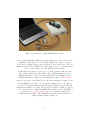
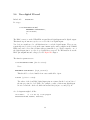
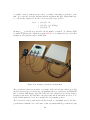
Figure 1.1: mini Netbook with USB4CH and geophone
One popular USB4CH configuration is with a mini Netbook for portable data
acquisition. In the photo above, the small cylinder is a geophone, a passive
sensor used for seismic surveys. A wide variety of other sensors can be used for
applications from DC to 10kHz. For software support, the Scope program can be
used to easily acquire, save, and display data in real time.
In this setup, the sensor is connected to one analog channel, while the other
three analog channels are still available. The red/black alligator pairs are
differential inputs for each of the analog inputs. The green alligator wire is
AGND, which is not required for a floating passive sensor. A GPS antenna
interface is provided on the DB25 for precision time stamping of acquired data.
The USB4CH is self powered. Power supplies varying from 8 to 24 volts are
acceptable. A 110 vac wall transformer is supplied with the system, with 220
transformers available on request. Various types of batteries can also be used for
power. As shown above, eight AA NiMH batteries will power the USB4CH for
over 20 hours. See powering with batteries for a discussion. Many other
configurations are possible. The USB4CH can be used with any Windows or
Linux computer having a USB port.
9
Chapter 2
Getting started
Installation of the USBxCH is fairly easy. Here are the steps to follow:
2.1
Find your CDROM
Look for a CD in the shipping box. This CD contains the system software and a PDF User
Manual with circuit diagrams. Support for both Windows and Linux is included on the
same disk. To install, change to the CD directory for the operating system you are going
to use, and at the command line run:
cmd:prompt>
install.bat
This will create the directory /SR/USBXCH on your hard disk, and unzip the CD files there.
This step only copies files to your hard disk. No registry entries or driver installation are
made with this step. If you don’t like running install.bat from the command line, use the
shortcut icon available on the CD. Once the files are copied to your hard disk, examine
the subdirectories. In particular, /SR/USBXCH/Driver will be needed later.
If you wish to remove the software from your system at this point, simply delete the
/SR/USBXCH directory. Nothing else is required. Later, after the device driver has been
installed, you must use the DevMan utility to completely remove the software.
The software must be installed in the /SR/USBXCH directory. Installation into other directories is not supported. Most of the executables can be run from any directory, but
the shortcuts and batch files have the standard path hardwired into them. If you need
to reinstall the software, rename or delete the current /SR/USBXCH directory and then run
install.bat again.
10
2.2
Downloading software from the web
If you want to upgrade to the latest software version, or simply want to review the product,
the full software package is available for free download from www.symres.com. The web
postings contain all the software and User Manual, but do not include circuit diagrams.
Full circuit diagrams are included only on the CD shipped with the system.
The symres.com web site has individual postings for each operating system as a zip file.
Download the appropriate file. Unzip the downloaded file into a temp directory and then
run install.bat to further unpack the software and create /SR/USBXCH.
2.3
Linux revs
The Windows drivers are compatible with all versions of XP/7. Unfortunately, Linux
drivers are specific to a particular version of the Linux kernel. Please compare your OS
kernel version with the SR driver build version. If they are different, you will have to
recompile.
Source code is provided so Linux users can rebuild for their particular kernel. SR attempts
to stay current with recent kernel revs, but does not offer support for older revs.
2.4
Hook up power
For connecting power to the USBxCH do the following:
√
Find the wall transformer
Look for the wall transformer included in the shipping box. US customers will
have a 110 vac unit, while international customers may have a 220 vac unit. The
output of the wall transformer should be rated at 9vdc 500ma.
Note that the USBxCH is not powered from the USB cable. You must use the
supplied wall transformer or other equivalent power source. In USB terminology,
the USBxCH is a self powered device.
√
Plug the wall transformer into the wall
Do not plug a 110 volt transformer into 220 power with simple adapters that do
not change the wall voltage. The wall transformer will simply output the wrong
voltage and probably burn up.
11
√
Plug the 2.1mm barrel connector into the USBxCH
Plug the 2.1mm barrel connector at the other end of the wall transformer cable
into either USBxCH back panel power jack. There are two jacks on the back
panel in parallel for daisy chaining power to other devices if needed. Make sure
the connector is fully seated into the jack.
√
Is the green LED on ?
If the wall transformer is energized at all, the green LED on the back panel near
the 2.1mm power jacks should light up. If the green LED is off, then there is a
basic problem with the wall transformer. Check the wall power and connections.
You must fix it to continue.
√
Is the red LED off ?
The red LED near the 2.1mm power jacks may momentarily light up when power
is applied, but will go off in a second or two. If the red LED stays on, it indicates
the power is not within specifications and something is wrong. Perhaps the wall
transformer voltage is low, or the USBxCH is suffering a short. If the red LED is
on, the problem must be fixed before the system will function correctly.
At this point, if the green LED is on, and the red LED is off, then the USBxCH is properly
powered and you are ready to connect the USB cable.
2.5
Hook up the USB cable
Connecting the USB cable is the big event. The PC will detect the new USB hardware
and prompt you for the location of its driver. The steps are:
√
Find the USB cable
Find the USB cable included in the shipping box. One end of the cable has a flat
type A USB connector for the PC. The other end has a square type B connector
for the USBxCH peripheral.
√
Plug the flat type A end into the PC
Plug the flat type A end into your computer. Note that the connector is polarized.
Do not use excessive force and plug it in upside down.
12
√
Plug the square type B end into the USBxCH
The next step is to plug the type B end of the USB cable into the powered up
USBxCH. Doing so will start a sequence of Plug and Play events. Keep an eye
on the PC when plugging it in.
√
Specify the driver directory to Plug and Play
After the PC has detected the new hardware, you will have to specify where it
can find the driver. For standard installations this is:
/SR/USBXCH/Driver
Once specified, the operating system will complete installation. Under Windows
this means the Plug and Play (PnP) manager will do the following:
Place a copy of the SrUsbXch.sys device driver file in the Windows
directory: /windows/system32/drivers.
Place a copy the SrUsbXch.inf driver info file in the Windows
directory: /windows/inf.
. . . the info file copy will be given a system generated name like:
oem1234.inf. The only sure way to find it is to compare file contents
with the original in /SR/USBXCH/Driver. Findstr or grep may help.
Linux carries out similar steps.
√
Check the Device Manager
Once PnP installation is complete, check the Device Manager to see the USBxCH
listed as an available device under the SR Instrumentation group.
Suppose you unplug the USBxCH and plug it into a different PC USB port. What will
happen? The PC will act as if new hardware has been detected and ask to reinstall the
driver all over again. Follow the above steps and all will go fine. If plugging and replugging
on the very same port, nothing will be required.
After the driver has been installed you will need to know the device name. Depending on
the number of systems installed this will be SrUsbXch0 (1,2,3 ...) etc. The device name
is required for later use with programs and library functions. If this is the first USBxCH
installed on the computer it will be:
SrUsbXch0
<< device name
13
To remove the driver, use the DevMan utility. It will delete the operating system copies of
the driver files and corresponding registry entries.
2.6
Run Diag
After hooking up power and connecting the USB cable, run the Diag utility to confirm
proper operation. This will check the hardware and give an error report if there are any
problems. Diag can be executed from the command line, or by double clicking on the
"Run Diag Install" shortcut icon. From the command line type:
cmd:prompt>
Diag install
Run Diag without any command line options for a help screen. If you feel the system has
a hardware problem, run Diag debug and email the report and log files to SR.
2.7
Run DVM or Scope
After running Diag, users should test acquiring data with DVM or Scope. Each comes in
both GUI and command line versions. For quick starts with default parameters, double
click on the shortcut icons.
When running, it is tempting to touch the analog input pins to apply small voltages. Avoid
the temptation to do this. You will inadvertently discharge static electricity into the inputs.
Even small static shocks such as those from walking on a carpet will do damage. Generally
the damage is cumulative, with calibration and analog performance steadily degraded with
each ESD event. If you must touch the input pins, touch the metal enclosure immediately
before doing so. This will help discharge any static. Better yet, wear an antistatic wrist
band clipped onto the front panel.
See the Analog inputs chapter for details on the analog input voltage ranges and differential
signals. For introductory hands on usage see the Examples and Experiments chapter.
2.8
Linux USB port permissions
Many Linux users will have installed the USBxCH driver while logged on as "root" and
all will run fine . . . but when they log on again as a regular user there will be trouble. The
problem is under Linux, there are not only file permissions, there are also USB hardware
port permissions. By default the hardware port permissions are often set to root, and if
you want to run as a regular user you will have to change them.
14
The steps for changing the Linux USB port permissions are covered in the file:
/usr/local/SR/USBXCH/Driver/"000 ReadMe.txt"
If you are already in the /usr/local/SR/USBXCH/Driver directory, the basic step is to
change the udev device rules. You can do so by executing:
cat 40-permissions.rules >> /etc/udev/rules.d/40-permissions.rules
and then rebooting as a regular user to reload the new rules. For Linux experts, the
contents of the 40-permissions.rules file are:
Contents of "40-permissions.rules" ...
# Symmetric Research USBxCH device - create with permission for all users
BUS=="usb", SYSFS(idVendor)=="15d3", SYSFS(idProduct)=="5504", MODE="0666"
15
Chapter 3
Application Programs
The USBxCH comes with three finished acquisition applications: DVM, Scope, and Blast.
With these programs you can acquire data, display it on the screen, and save it to disk.
Even for those planning to write their own custom software, running these applications will
help you understand how the system works.
The DVM program presents its data on the screen in familiar digital voltmeter style and is
suitable for low sampling rates. The Scope program presents its data as horizontal traces
in oscilloscope fashion and is suitable for low and medium sampling rates. Both DVM and
Scope specify their acquisition parameters with initialization files (ini files), and come in
graphical (GUI) and text only (command line) versions. The Blast program is a minimal
command line only program. All of its acquisition parameters are specified on the command
line, and it saves its data in packet format exactly as received from the USBxCH. Blast is
appropriate for all sampling rates up to the maximum the system bandwidth can support.
Source code for each of these programs is included with the system, and is also available
for download at www.symres.com.
The following sections give details about DVM, Scope, and Blast. The Calibrate program
is for use with DVM and is also detailed here. For information about general utility and
format conversion programs see Chapter 4, Utilities and Format conversion.
.
DVM
enhanced multichannel digital voltmeter
.
Calibrate
DVM calibration into volts and user units
.
Scope
horizontal real time trace display
.
Blast
minimal but fast PAK file acquisition
16
3.1
DVM
DVM is an acquisition program for the USBxCH with a display and function much like an
enhanced multichannel digital volt meter. If hand held instruments such as Fluke meters
are familiar, then you will find DVM easy to use.
One feature of DVM is besides displaying values as counts or volts, it can also display
values in user specified units. For example, displays reading in degrees C are possible. A
calibration program is included to easily generate the coefficients for such setups.
DVM optionally saves its acquired values to ASCII disk files. This makes it easy to review
experimental results, and to import data into spreadsheets etc. See the Examples and
Experiments chapter for an example of importing data into GnuPlot.
DVM comes in two versions. A full GUI (graphical user interface) display, and a text only
command line version. Both versions take their setup parameters from an ini initialization
file. The ini syntax and keywords are the same for both. The following sections review
details of using the program.
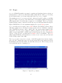
Figure 3.1: Typical DVM GUI display
17
3.1.1
DVM: starting the program
Starting DVM is similar for either the GUI or text only versions. From the command line
type either of:
cmd:prompt>
DvmGui parameters.ini
cmd:prompt>
DvmCmd parameters.ini
where the first is for the GUI display and the second for the text only display. The
parameters.ini file is optional. If not specified, DVM will start up with defaults. If you
want to run with custom parameters, they should be specified in the ini file. There is
nothing special about the ini filename, any filename may be used. In fact, having several
ini files for different setups can be very handy.
Several program shortcuts are also included in the DVM directory. Double click on them
to execute. Copy the shortcuts to the Windows Desktop or Start menu for easy access if
needed. You can also make multiple copies of the shortcuts and edit their properties to
run with different ini files.
18
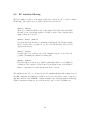
3.1.2
DVM: ini syntax
The layout of a DVM ini file is free format ASCII with a simple syntax of the form:
keyword = value
Comments are denoted with a semicolon, where everything from ; to the end of line is a
comment. You can create and edit ini files with text editors such as Windows Notepad or
any other favorite editor. For a listing of all the DVM ini keywords, see the file:
/SR/USBXCH/Dvm/DvmHelpIniSyntax.txt
Keywords not specified in the ini file will be given default values. Here is an example of a
short ini file:
; short DVM ini file:
; custom channel 0 display parameters ...
ChannelTitle
ChannelUnits
ChannelPlaces
ChannelDigits
ChannelSlope
ChannelOffset
0
0
0
0
0
0
=
=
=
=
=
=
"Temp"
"Degree F"
5
0
-0.0007109
631.757
;
;
;
;
;
;
any string
any string
total # digits shown including .
# digits after .
calibration slope
calibration offset
; channel 1,2,3 are not specified and stay at default values ...
All DVM parameters are taken from the ini file or default program values. Changes
to parameters such as the number of digits displayed must be specified in the ini file.
There are no GUI dialogs for setting ini parameters such as displayed digits. To make
changes, edit and reload the ini file. Besides the keywords in the fragment above, there are
also keywords specifying the output filename, time format, and similar features. See the
DvmHelpIniSyntax.txt file.
Note the DVM sampling rate is fixed at 1Hz, and is not specified with a keyword. DVM
is intended for low acquisition rate applications. Use Scope or Blast for support at user
specified sampling rates.
19
3.1.3
DVM: GUI version
When run in GUI mode, the DVM screen will look like:
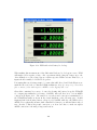
Figure 3.2: DVM GUI screen
For a USB4CH, all four analog channels are displayed as green digital readouts. The
channel titles are on the left and display units on the right. The titles and units can be
specified independently for each channel in the DVM ini file.
Across the top of the screen is an Alt menu with various program actions. With the Alt
menus you can start and stop acquisition, edit the ini file, and bring up a help screen. Each
Alt menu item has a speed key for keyboard users. Note that even the ini editor can be
specified in the ini file. Notepad is only the default.
Users wanting to change the display units will need calibration coefficients. The DVM
Calibrate program can be used to compute the required slopes and offsets and automatically
save them to an ini file.
20
3.1.4
DVM: command line version
If you like the data acquired by DvmGui, but only want to run a modest user interface
without a full graphical display, then the DvmCmd text only version of the program may
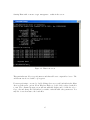
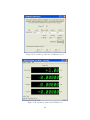
be useful. The DvmCmd output screen looks like this:
Figure 3.3: DVM CMD text screen
If you don’t even want this amount of display, there are ini keywords to turn the display
off entirely. This can be useful for lower power computers only wanting to save their data
to a file. The DvmCmd executable size is also smaller than DvmGui.
Note that DvmCmd uses the same ini keywords as DvmGui. You can refine keyword
selections with DvmGui and then move over to DvmCmd without change.
21
3.1.5
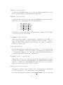
DVM: ASC output file format
DVM can save its acquired results to ASCII disk files. To turn file saving on, set the ini
keyword:
OutputFileName = "myfile.asc"
The output file may be given any name, but it is conventional to use the .asc extension for
easy identification. You can give the empty string "" or value ”NONE” for no file.
There are also ini keywords to control the output file format. Items such as header format
and time display may be selected. See the file DvmHelpIniSyntax.txt for a complete
syntax description. The general format of an ASC file is fairly simple. Data is laid out in
columns, one column per channel, and one sample point per row:
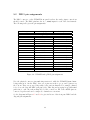
DVM ASC output file layout:
channel
channel
channel
channel
channel
channel
channel
channel
channel
channel
channel
0,
0,
0,
0,
0,
0,
0,
0,
0,
0,
0,
channel
channel
channel
channel
channel
channel
channel
channel
channel
channel
channel
1,
1,
1,
1,
1,
1,
1,
1,
1,
1,
1,
channel
channel
channel
channel
channel
channel
channel
channel
channel
channel
channel
2,
2,
2,
2,
2,
2,
2,
2,
2,
2,
2,
channel
channel
channel
channel
channel
channel
channel
channel
channel
channel
channel
3,
3,
3,
3,
3,
3,
3,
3,
3,
3,
3,
HMS:YMD
HMS:YMD
HMS:YMD
HMS:YMD
HMS:YMD
HMS:YMD
HMS:YMD
HMS:YMD
HMS:YMD
HMS:YMD
HMS:YMD
... etc
For DVM, each row advances by 1 second. If the acquisition units are volts, then the
voltages from channel 0 will be lined up in the first column. Channel numbering starts at
0. Files in this type of column format are easily imported into spreadsheets and analysis
programs such as GnuPlot, Excel, or Matlab for plotting and processing.
See the Examples and Experiments chapter for examples of using the public domain plotting
program GnuPlot and many other applications.
22
3.1.6
DVM: Calibrate
Sometimes users are surprised to learn A/D converters do not output their results as volts.
The output from an A/D converter is actually a digital integer that is only proportional to
the input voltage. The conversion from this digital integer to units such as volts is referred
to as the calibration.
The concept of calibration for an A/D converter can be carried even further into physical
sensor units. Suppose you have a sensor like a potentiometer or temperature gauge. At
the minimum setting the sensor may result in a particular A/D count, and likewise at its
maximum setting another count value. These two points define a line, and conversion of
the count values directly into sensor units, such as potentiometer turns or ◦ C can be done
with a linear transformation having a slope and offset.
The Calibrate program makes it easy to obtain the slope and offset coefficients for such
transformations. It allows you to record the transducer min and max settings, and then
output an ini file for use with DVM. The Calibrate screen looks like this:
Figure 3.4: DVM Calibrate screen
To start the program, execute either CalGui.exe or CalCmd.exe from the command line,
or double click on one of the provided shortcuts. Approximate calibration into volts is
provided in the DvmSetupVolts.ini file included with the software. However, because
23
all A/D converters, references, and resistors have tolerances, precision calibration must
be performed on each individual system and channel. Absolute calibration requires a lab
grade reference with repeatable fixed voltages. For such applications, the SR VREF-399
heater stabilized precision reference may be useful, see www.symres.com. Applications not
requiring absolute calibration may find ratiometric techniques helpful.
See the Examples and Experiments chapter for an absolute calibration demo, an example
of calibration into physical sensor units, and a ratiometric experiment. For a discussion of
the number of A/D counts per volt see the Analog DC calibration chapter.
24
3.2
Scope
Scope is a USBxCH acquisition program for acquiring and displaying data in real time as
horizontal traces on the screen. The functionality is much like an oscilloscope. If viewing
the AC characteristics of your data is important, then Scope is a good match.
The sampling rates for Scope are user selectable, with rates from the low Hz to several kHz
supported. Analog response is to DC, which means even if sampling at kHz, DC inputs will
still return the same correct DC value over and over on each sample. The Scope real time
graphical display requires considerable PC CPU horsepower which may limit achieving the
highest USBxCH rates. For the maximum sampling rates, use the Blast program.
Scope optionally saves its acquired data to DAT disk files. The DAT file format is binary
with data organized as records that are demuxed at the bit level. DAT files contain the
entire USBxCH data stream: analog, digital, GPS, and system status parameters like
temperature. For easy post processing, two utility programs are provided. The Dat2Asc
utility converts binary DAT to ASCII text files readable in any text editor. Dat2Asc files
can also be imported into programs such as GnuPlot, Excel, and MatLab. The View
utility displays DAT files as horizontal traces on the screen so users can scroll back and
forth reviewing acquired data offline.
The Scope program comes in two versions. A full GUI graphical user interface display,
and a text only command line version. Both versions take their setup parameters from an
ini initialization file much like DVM, but with different keywords. The following sections
review particular aspects of running Scope.
Figure 3.5: Typical Scope display
25
3.2.1
Scope: starting the program
Starting Scope is the same for either the GUI or the text only version, and is similar to
starting DVM. From the command line type one of:
cmd:prompt>
ScopeGui parameters.ini
cmd:prompt>
ScopeCmd parameters.ini
where the first is for the GUI display and the second for the text only display. The
parameters.ini file is optional. If not specified, Scope will start up with defaults. If you
want to run with custom parameters, they should be specified in the ini file. There is
nothing special about the ini filename, any filename may be used. In fact, having several
ini files for different setups can be very handy. The GUI and command line versions of the
program use the same ini keywords.
Several program shortcuts are also included in the Scope directory. Double click on them
to execute. Copy the shortcuts to the desktop or start menu for easy access if needed.
Make copies of the shortcuts and edit their properties to run with custom ini setups.
26
3.2.2
Scope: ini syntax
The layout of a Scope ini file is similar to that for DVM, only the keywords are different.
Scope ini files are free format ASCII with a simple syntax of the form:
keyword = value
Comments are denoted with a semicolon, where everything from ; to the end of line is a
comment. You can create and edit ini files with text editors such as Windows Notepad or
any other favorite editor. For a listing of all the Scope ini keywords, see the file:
/SR/USBXCH/Scope/ScopeHelpIniSyntax.txt
Here is an example of a short ini file:
; short Scope ini file:
SamplingRate = 130.0
ToggleLed = ON
; requested sampling rate
ChannelTitle
ChannelTitle
ChannelTitle
ChannelTitle
0
1
2
3
=
=
=
=
"Channel Name 00"
"Signal Generator 0"
"Microphone"
"My custom name"
DigitalTitle
DigitalTitle
DigitalTitle
DigitalTitle
0
1
2
3
=
=
=
=
"DIG0"
"DIG1"
"DIG2"
"DIG3"
; analog display names
; digital display names
OutputFileFormat = Dat
OutputFileNaming = Sequential
; Dat, None
; Single, Sequential, Time
; all other keywords are not specified and stay at default values ...
Keywords not specified in the ini file will be given default values. There are no GUI dialogs
for setting ini parameters, with the exception of a few display settings that can be toggled
with Alt menu commands. All other Scope parameters are taken from the ini keywords or
default values. Alt menu commands are available for quick ini file editing and reloading.
27
3.2.3
Scope: GUI version
When run in GUI display mode, the Scope screen will look like:
Figure 3.6: Scope GUI screen
The four analog channels are displayed as horizontal traces, as well as the digital channels
and GPS data too. The channel titles and enabling/disabling the display of particular
channels can be specified in the ini file.
Across the top of the screen is an Alt menu with various program actions. With the Alt
menus you can start and stop acquisition, edit the ini file, and bring up a help screen.
Speed keys are available for keyboard users. As with DVM you can specify the text editor
to use.
To change the Scope sampling rate you must edit and reload the ini file. Only rates from
the Rate Table are permitted. Requested rates not on the rate table will be rounded to the
nearest allowed rate. The sampling rate and other system parameters appear in the status
bar at the bottom of the Scope window.
28
3.2.4
Scope: command line version
If you like the capabilities of ScopeGui, such as specifying sampling rates and DAT files,
but want a text only display, then ScopeCmd may be a good match. The ScopeCmd screen
looks like this:
Figure 3.7: Scope CMD screen
If you don’t want even this amount of display, there are ini keywords to turn the display
off entirely. This can be useful for headless node single board computers only wanting to
save their data to a file.
Note that ScopeCmd uses the same ini keywords as ScopeGui. You can refine keyword
value selections with ScopeGui and then move them over to ScopeCmd without change.
29
3.2.5
Scope: output file names
Scope output files are saved to disk in the DAT file format. This is a binary format
comprised of a header and data records, as described in the next section. This section
describes the Scope output file name conventions.
Two ini keywords control the output file names and size:
OutputFileNaming
OutputFileNbuffers
=
=
{NONE,YMDHMS,SINGLE}
N
OutputFileNaming specifies how individual output files are named. As Scope runs, it fills
a temporary file Scope.tmp, and when full renames it according to:
NONE: turns off file output altogether. Use this option if you are setting Scope up
for an experiment and don’t want to save data yet.
YMDHMS: (default) creates a data subdirectory for the current Scope run with the
name (year, month, day, hours, minutes, seconds) as given by the PC clock. Within
the YMDHMS data directory, data is saved to Scope.tmp as it comes in. When filled,
the temp file is renamed to nnnnnnnn.DAT with an 8 character sequential decimal
name starting at 00000000.DAT. A new YMDHMS data directory is created for
each Scope Ctrl+R run and the sequential names will start again at 0. This filename
convention is similar to the Blast output filename convention.
SINGLE: renames the temporary file Scope.tmp to the single file named Scope.dat.
You or downstream processing must remove Scope.dat before the next file is ready
or an error will occur.
OutputFileNbuffers specifies the output file size. It controls how many acquisition buffers
are saved to Scope.tmp file before it is given its permanent name and a new temp file is
started. N can be any value between 1 and 4,294,967,295 (unsigned long).
The number of data samples per acquisition buffer varies with sampling rate and is selected
so each buffer is about 1/2 second long. At a sampling rate of 130 Hz, for example, there
will be 64 samples for each channel in one buffer. While at sampling rate of 2604 Hz, there
will be 1302 samples for each channel in one buffer.
For more information on these and other ini keywords, refer to the file:
/SR/USBXCH/Scope/ScopeHelpIniSyntax.txt
30
3.2.6
Scope: DAT output file format
The binary DAT file format saves complete information about a data run, including analog,
digital, GPS, and status parameters like temperature. Because binary files are smaller than
ASCII, CPU and disk bandwidth requirements are reduced when saving data in real time.
Most users will find it easiest to review DAT files by using the Dat2Asc and View utilities.
With these utilities you don’t need to know the internal binary structure of the DAT file
to do offline downstream processing.
For those who are interested, the internal structure of a DAT file is detailed in the include
file:
/SR/USBXCH/Include/SrDat.h
You may also wish to refer to the Dat2Asc.c source code for an example of how to decode
the DAT data records. In general, a DAT file is comprised of a 4096 byte header, followed
by data records.
The header itself is comprised of a C structure, SrDatHdrLayout, followed by zero padding
to fill out the 4096 bytes. The fields in the header include items such as sampling rate,
number of channels, etc. All of the the Scope ini keyword values are recorded in the header
for a complete record of the acquisition run associated with the DAT file.
Data records follow the header and may have many different types of data. Analog, digital,
GPS, and system information are all encoded in the records. Each data record starts off
with a record tag giving the data type, and then the record information.
The record tag is itself a structure with an integer id indicating the type of record information following the tag structure. The following are a few of the record tag types:
#define
#define
#define
#define
#define
SRDAT_TAGID_USBPACKET
SRDAT_TAGID_USBANALOG
SRDAT_TAGID_USBSERIAL
SRDAT_TAGID_USBEQUIP
SRDAT_TAGID_EOF
((long)(’BSUT’))
((long)(’ABUT’))
((long)(’SBUT’))
((long)(’EBUT’))
((long)(’FOET’))
//
//
//
//
//
=
=
=
=
=
"TUSB"
"TUBA"
"TUBS"
"TUBE"
"TEOF"
Refer to SrDat.h for a listing of all the record tags. Not all of the record types may appear
in a specific DAT file. Within a record, data may be arranged according to the specific
record type. See Dat2Asc.c for a decoding example.
Note that because the DAT files have a header, they cannot be concatenated from the
command line with the > copy command. Instead, use the Dat2Asc sequential processing
feature to process multiple files.
31
3.3
Blast
Blast is a USBxCH acquisition program designed to use the minimum PC resources possible.
It is started from the command line and saves its data to disk as PAK files comprised of
native USB binary packets.
The sole purpose of Blast is to save data to disk quickly. It does not have a GUI display or
even a real time text display of the data. If you need a text display of the data, please refer
to DvmCmd or ScopeCmd. Because it uses the minimum PC resources possible, Blast is a
good match if you need to make the most of the CPU and disk bandwidth available on a
particular computer.
Use the Pak2Asc and View utilities for easy ways to review PAK output files. If you are
writing custom software, Blast is also a good example to use as a starting point for your
source code development. By comparison, DVM and Scope have much more complicated
user interfaces. The following sections review particular aspects of running Blast.
Figure 3.8: Typical Blast display
32
3.3.1
Blast: starting the program
Start Blast from the command line. There is no ini file associated with Blast as with DVM
or Scope. All user options are specified on the command line. The syntax is:
cmd:prompt>
Blast sn [gn] [nFiles] [nokeypress] [0xUC] [/?]
where [ ] indicates the parameter is optional. Running without any command line parameters or /? will give a usage message. The other command line parameters are:
"sn": specifies the USBxCH sampling rate and must be one of the following:
Blast sampling rate table:
sn
s1
s2
s3
s4
s5
s6
s7
s8
s9
s10
s11
->
SPS(Hz)
19.531250
32.552083
39.062500
65.104167
78.125000
130.208333
651.041667
1302.083333
2604.166667
4882.812500
9765.625000
PACKETS/FILE
47
64
78
97
117
130
651
1302
1302
2441
4882
BYTES
3008
4096
4992
6208
7488
8320
41664
83328
83328
156224
312448
~ SECONDS
5
4
4
3
3
2
2
2
1
1
1
Specifying the "sn" sampling rate also automatically sets the output file size. The output PAK files are measured in USB packets, with 64 bytes per packet. The approximate
number of seconds of data in each output file is also listed.
"gn": specifies the time source to use and must be one of the following:
Time source table:
g0
g1
g2
g3
->
->
->
->
NONE
PCTIME
GARMIN
TRIMBLE
<< default
( NMEA = RMC, GGA )
( NMEA = ZDA, GGA )
If you have a GPS antenna, specify the proper "gn" number to generate time stamps
based on its signals. For users without GPS antennas, the PCTIME option uses the PC
33
clock as the time source. Note that if PCTIME is the time source, then the PC clock
will provide time, even if a GPS antenna is connected to the system. To process GPS
time you must specify a GPS source. For details about using GPS with the USBxCH,
see the GPS Time Stamping chapter.
nFiles: specifies how many total output files will be created. Blast will terminate
once nFiles have been written. If nFiles is not given, the program will create output
files forever, or until a keypress is made. You can also terminate the program from the
operating system with Task Manager.
nokeypress: specifies Blast is to start acquiring data with no keypress required. The
default behavior waits for a keypress to begin acquiring so you can have a chance to
read the on screen run time summary message.
UserCfg: is passed to the Open function inside Blast. See the User C Library for
information about Open, and the User configuration byte for bit assignments. UserCfg
should be a two digit C style hex number, like 0x14.
When staring up, Blast will display a summary report of the parameters it is running
with on the screen. This gives you an opportunity to verify the system is actually using
the parameters specified on the command line. A copy of the summary report with the
filename "000 Blast Run Summary.rpt" is also placed in the YMDHMS data directory
for a permanent record of the run.
After the summary display, output files will be listed on the screen as they are created.
Output files are all placed in the YMDHMS data directory for the particular run. See
the next section for a complete description. Each time Blast runs, a new data directory is
created. When running with nFiles not specified, output files will be created forever. You
can terminate the run by pressing ’q’ on the keyboard, or killing the Blast process with
the Task Manager.
A few typical Blast command lines are:
blast
blast
blast
blast
blast
blast
blast
s3
s3 g0
s3 g2
s10 nokeypress
s11 0x04
s8 100
s8
<
<
<
<
<
<
<
acquire
acquire
acquire
acquire
acquire
acquire
acquire
at 39Hz, use PC TIME
at 39Hz, without any time stamps
at 39Hz, with a Garmin antenna
at 4.8kHz, no keypress to start
at 9.7kHz, enable Adrdy on DB25
100 files at 1.3kHz
forever at 1.3kHz, ’q’ quits
34
Starting Blast with: > blast s7 g2 nokeypress results in the screen:
Figure 3.9: Blast text screen
This particular run did not specify nFiles and thus will create output files forever. The
endless run was aborted with a ’q’ keypress.
For users preferring to execute by double clicking, there are several batch files in the Blast
directory with preset options. From Windows Explorer, double click on these batch files
to run. The command prompt screen will automatically display and look like the above.
Copy, edit, and change the batch files if you wish to run with with other parameters. You
may also create shortcuts to the batch files.
35
3.3.2
Blast: output file names
Blast output files are saved to disk in the PAK file format. This is a binary format comprised of 64 byte packets exactly as received from the USB cable. Packet format is briefly
summarized in the next section. This section describes the output filename conventions.
When Blast is started, a data directory with the name YMDHMS is automatically created.
YMD stands for (year, month, day) and HMS for (hours, minutes, seconds). The data
directory name is formatted as:
2009-05-01-at-23-11-06
which should be read as: a Blast run was started on (2009/05/01) at (23:11:06). The
YMDHMS convention keeps the data directories well ordered when sorted by name. Within
a data directory for a particular run, Blast creates sequential file names like:
./2009-05-01-at-23-11-06/00000000.PAK
./2009-05-01-at-23-11-06/00000001.PAK
./2009-05-01-at-23-11-06/00000002.PAK
./2009-05-01-at-23-11-06/00000003.PAK
./2009-05-01-at-23-11-06/00000004.PAK
./2009-05-01-at-23-11-06/00000005.PAK
etc ...
The location ./ is where Blast was started. The next time Blast is run, a new data directory
will be created with the new YMDHMS start time, and the sequential file names will start
all over again at 00000000.PAK.
Output files are fixed in size as described in the previous section. Use the Pak2Asc utility
to convert an entire series of sequential PAK files to ASCII format with one call.
If necessary, PAK files can be concatenated with the copy command. Because they are
binary, you must use the copy /b option. End of file ctrl+z characters are inevitably
buried in the binary PAK data and the /b option is required to process them correctly.
PAK files must also be concatenated in acquisition order. If two files are concatenated in a
different order than they were acquired, then the error correction codes will not track. As
an example, if you have a directory with a long sequence of files then the command:
cmd:prompt>
copy /b 0*.PAK OneSingleFile.pak
will concatenate all of them into a single PAK file which can be further processed. Usually
concatenation is not required when using Pak2Asc.
36
3.3.3
Blast: PAK output file format
Data is transmitted from the USBxCH to the PC in 64 byte packets over the USB cable. To
maximize bandwidth, Blast saves these native packets directly to its output files without
any processing. The output files are all given the PAK filename extension to make them
easy to identify. PAK stands for packet format.
A USBxCH packet has considerable internal structure. Within the 64 bytes, the data could
be analog, digital, GPS PPS, GPS NMEA strings, system status, or error correction codes.
Each packet has headers to identify its type and substructure. For most users, the easy
way to deal with PAK files is to use the Pak2Asc or View conversion utilities.
For those who are interested in the binary PAK format, here is the layout:
Work underway . . .
37
3.3.4
Blast: typical post processing
Beyond Pak2Asc and View, users may want to automate post processing data from multiple
acquisition runs. One way is to use batch files to customize the data flow to exactly fit
your needs. This section covers a few techniques.
Suppose you have data from several acquisition runs in YMDHMS directories:
2009-09-21-at-11-32-45/
2009-09-21-at-11-33-26/
2009-09-21-at-11-33-41/
2009-09-21-at-11-58-15/
2009-09-21-at-13-40-36/
2009-09-21-at-15-03-47/
2009-09-21-at-15-20-15/
...
...
...
...
...
...
...
where ... indicates there are many sequential files in each directory. It is hard to know
what all the directory names are, and you probably don’t want to type them in with each
new set of runs. To process all of these directories automatically, use a text editor to put
the following line in a file:
@for /D %%i in (20??-*) do Pak2Asc.exe %%i/00000000.pak fw
Usually batch files are given a .bat extension. To execute a batch file, type its filename
on the command line, or double click from Windows Explorer. In the @for line, parameter
replacement will be done on the %%i variable, invoking the command following the do on
every directory matching the wildcard pattern (20??-*). The batch file:
Pak2Asc Convert All.bat
in the Blast directory implements the @for line given above. In batch file programming,
the command following "do" can even be comprised of many subcommands using &. For
example, the following:
@for /D %%i in (20??-*) do cd %%i & ren *.pak *.bin & cd ..
would descend into each directory and rename all the pak files to have a .bin extension.
With batch files you can process a great deal of data very quickly.
For information about batch file programming search on phrases like "command-line
reference" or "batch files" in the Windows help system. Linux also has similar command line script programming.
38
3.3.5
Blast: running in the background
For many applications, running Blast as a background task is useful. Under Windows use
the Task Scheduler to setup Blast as a background job. With Task Scheduler, you can start
at a specified time, periodically, or automatically on startup. All quietly in the background
while the computer can attend to other tasks. Under Linux, use the & command line
qualifier. The USBxCH on board FIFO makes it unlikely any data will be lost even if the
PC cannot serve the Blast background task immediately.
One problem that comes up with background execution is what to do with screen output.
The solution is to redirect any screen display to a file with the > operator. The following
would be typical:
cmd:prompt>
Blast s4 nokeypress > report.txt
Besides saving screen output in the report.txt file, the Blast nokeypress option will start
acquisition with no keyboard interaction required. Note that the above Blast command
line runs continuously, saving files until the process is killed with Task Manager or the
taskkill command. From Linux use the kill command.
39
Chapter 4
Utilities and Format Conversion
Besides the DVM, Scope, and Blast applications, several smaller utilities are also provided
for use with the USBxCH. They cover a number of basic tasks, with most intended for
processing data offline once it has been acquired. Popular utilities are Dat2Asc and Pak2Asc
for converting binary DAT and PAK files to ASCII. Other utilities are:
.
Diag
general system hardware diagnostic
.
DevMan
USBxCH device driver management
.
Dat2Asc
convert Scope binary DAT data files to ASCII
.
Pak2Asc
convert Blast binary PAK data files to ASCII
.
Interpolate
change time base and sampling rate of saved DAT files
.
View
review and display DAT and PAK files
.
NmeaTime
report the NMEA strings / set PC time for systems with GPS
.
GpsProg
program a GPS antenna through the USB port
.
DigitalIo
twiddle the DB25 digital io bits
.
SetDid
set the USB DID for multiboard installations
Source code is included, and users are encouraged to use it as a starting point for developing
their own custom utilities. There may be additional utilities available with the software
distribution besides those listed above, see the ReadMe.txt files for information.
Most of the utilities are command line oriented, and have options that may be specified.
Executing without any options will give a help screen. Under Windows, shortcut icons are
also available that may be double clicked to run with defaults. The following sections cover
each utility and their options.
40
4.1
Diag
Diag should be used to verify correct operation of the USBxCH after installation or if you
ever have any doubts about the hardware. It is the Swiss Army knife of USBxCH hardware
maintenance.
The Diag command line syntax is:
cmd:prompt>
Diag test [gn] [driver] [/?]
where [ ] indicates the parameter is optional. Running without parameters or with /?
will give a usage message. The other command line parameters are:
test: is required and specifies the particular test to run. The following are a few of
the available tests. See the /? usage message for the full list:
install
debug
dev
power
led
analog
nmea
equip
digin
digout
dram
rev
reset
=
=
=
=
=
=
=
=
=
=
=
=
=
Installation test suite (dev,power,led,analog,nmea)
Debug tests for customer support
Show device descriptor
Check if power is good
Toggle the yellow LED
Start A/D’s and display analog data
Start A/D’s and display NMEA strings
Start A/D’s and display equipment info like temp
Read digital input
Send digital output
Run several DRAM FIFO tests
Get firmware revision number
Hardware reset USBxCH board with full power cycle
gn: specifies a time source. If not specified, the PC clock will be used as the time
source. See GPS Time Stamping for more information.
g1
g2
g3
->
->
->
PCTIME
GARMIN
TRIMBLE
( NMEA = ZDA )
<< default
( NMEA = RMC, GGA )
( NMEA = ZDA, GGA )
driver: this option is required only if you are running multiple USBxCH boards on
a single PC with the names ( SrUsbXch0 .. SrUsbXch9 ). For a list of installed
driver names use the DevMan utility. See SetDid for specifying the name associated
with a particular board. Single board users should not specify this parameter, accepting
the factory default SrUsbXch0.
41
As part of any new installation, users should run:
cmd:prompt>
Diag install
This carries out a series of tests to confirm the driver is correctly installed and the basic
hardware is functioning. Windows users may also double click on the "Run Diag Install"
shortcut rather than executing from the command line.
If you feel the USBxCH has developed a hardware problem after running successfully for
awhile, then run:
cmd:prompt>
Diag debug
and email the files:
/SR/USBxCH/Utilities/Diag/"300 Diag History.log"
/SR/USBxCH/Utilities/Diag/"301 Diag Last Run.rpt"
to Symmetric Research for technical help. Do not delete earlier entries in the history log.
They may provide clues for debugging.
SR help email address:
42
[email protected]
4.2
DevMan
DevMan is a command line utility to manage USBxCH device drivers once installed on a
PC. For initial driver installation rely on the operating system Plug and Play capabilities
as described in the Getting started chapter.
The DevMan command line syntax is:
cmd:prompt>
DevMan [showall] [wakeall] [removeall] [/?]
where only one optional parameter may be specified at a time, and running without any
options or with a /? will give a usage message. The parameters are as follows:
showall: scans the registry for all USBxCH references, showing both active and
inactive instances. Also shows the related sys and inf files in the Windows driver
directories. Plugging a USBxCH into different USB ports on the PC results in an
instance of the USB driver each time. This option shows all symbolic device names,
and current status for each instance.
wakeall: if the PC is put into a sleep state while USBxCH devices are plugged in
and active, they will not be active on wakeup. This is an acknowledged OS level error
for Windows and self powered USB devices. Running DevMan wakeall will wakeup
all connected USBxCH devices after PC sleep.
removeall: deletes all USBxCH registry entries, and all driver sys and inf files in
the Windows directories. If you want to clean the system of earlier driver revisions
and force plug and play to load a new driver version, then use removeall.
Many of the tasks addressed by DevMan can also be carried out by hand in the Windows
GUI Device Manager. Using the DevMan command line program is safer for most users,
since its operations are specifically targeted at the USBxCH. It is difficult to compromise
the computer with DevMan, while with Windows Device Manager you are exposed to
drivers for all the hardware serving the system.
If you have forgotten the symbolic device name of a particular USBxCH, use the showall
option to refresh yourself. For information on running multiple USBxCH systems on a
single PC refer to the Examples and Experiments section Multiple USBxCH.
43
4.3
Dat2Asc
DatAsc converts the binary DAT files generated by programs like Scope to ASCII format.
The ASCII output is in columns that are easily readable in a text editor, as well as being
suitable for importing into spreadsheet and analysis programs.
The Dat2Asc command line syntax is:
cmd:prompt>
Dat2Asc filename format [/?]
where the filename and format parameters are required. Running without parameters or
with a /? will give a usage message. The filename and format are as follows:
filename: specifies the DAT input file. A .dat filename extension is customary
but not required. If the input file is not in DAT format, Dat2Asc will detect it and
terminate with an error. A full file pathname may be given, and then both the input
and output are directed to the indicated path.
If the filename has the form nnnnnnnn.dat, sequential processing is initiated, and
Dat2Asc will automatically look for and process the n+1 file. For sequential mode,
the starting filename must be eight decimal digits with a .dat extension. Note the
filename 0.dat has fewer than eight decimal digits and will not initiate sequential
processing.
format: specifies the ASCII output format, where format may be:
fw
fw_hex
fw_debug
csv
csv_hex
csv_debug
raw
=
=
=
=
=
=
=
fixed width ASCII columns
fw with hex instead of decimal fields
fw with low level debugging info
comma separated values
csv with hex instead of decimal fields
csv with low level debugging info
record format, for debugging only
The fixed width formats are easy to view by eye in text editors, while the csv formats are
easiest to import into downstream processing programs like GnuPlot and Excel. A typical
Dat2Asc command line for sequential processing might be:
cmd:prompt>
Dat2Asc ./mydatadirectory/00000000.dat csv
44
this will convert all of the sequential files in mydatadirectory, leaving the results there in
a single large ASCII file. Conversion is a multipass process with intermediate files. The
names of the files created by Dat2Asc are:
Dat2Asc-100-TimeInfoSample.asc
Dat2Asc-101-TimeInfoStatus.asc
Dat2Asc-102-TimeInfoEquip.asc
Dat2Asc-200-TimeInfoAll.asc
Dat2Asc-300-Nmea.asc
Dat2Asc-301-Data.asc
The last file, Dat2Asc-301-Data.asc, is the name of the final large output file with all of
the combined data. For csv formats, the final data file will be given a .csv extension. The
intermediate files may also have information you find useful.
Dat2Asc has verbose screen output. It reports the input files it processes, information
about each processing step, and the files created. To run silently, simply redirect the
screen output to a report file with:
cmd:prompt>
Dat2Asc 00000000.dat fw > dat2asc.rpt
Techniques for automating the processing of data from multiple acquisition runs is covered
in the Blast section typical post processing. For a ready to go example see the batch file:
/SR/USBXCH/Utilities/Scope/"Dat2Asc Convert All.bat"
For an example of importing ASCII data into a plotting program see the Examples and
Experiments section GnuPlot. The techniques used with GnuPlot are similar to those that
would be used with other plotting and analysis programs.
45
4.4
Pak2Asc
Pak2Asc converts the binary PAK files generated by programs like Blast to ASCII format.
The ASCII output is in columns that are easily readable in a text editor, as well as being
suitable for importing into spreadsheet and analysis programs.
The Pak2Asc command line syntax is:
cmd:prompt>
Pak2Asc filename format [/?]
where the filename and format parameters are required. Running without parameters or
with a /? will give a usage message. The filename and format are as follows:
filename: specifies the PAK input file. A .pak filename extension is customary
but not required. If the input file is not in PAK format, Pak2Asc will detect it and
terminate with an error. A full file pathname may be given, and then both the input
and output are directed to the indicated path.
If the filename has the form nnnnnnnn.pak, sequential processing is initiated, and
Pak2Asc will automatically look for and process the n+1 file. For sequential mode,
the starting filename must be eight decimal digits with a .pak extension. Note the
filename 0.pak has fewer than eight decimal digits and will not initiate sequential
processing.
format: specifies the ASCII output format, where format may be:
fw
fw_hex
fw_debug
csv
csv_hex
csv_debug
raw
=
=
=
=
=
=
=
fixed width ASCII columns
fw with hex instead of decimal fields
fw with low level debugging info
comma separated values
csv with hex instead of decimal fields
csv with low level debugging info
packet format, for debugging only
The fixed width formats are easy to view by eye in text editors, while the csv formats are
easiest to import into downstream processing programs like GnuPlot and Excel. A typical
Pak2Asc command line for sequential processing might be:
cmd:prompt>
Pak2Asc ./mydatadirectory/00000000.pak csv
46
this will convert all of the sequential files in mydatadirectory, leaving the results there in
a single large ASCII file. Conversion is a multipass process with intermediate files. The
names of the files created by Pak2Asc are:
Pak2Asc-100-SamplePackets.pak
Pak2Asc-101-StatusPackets.pak
Pak2Asc-200-TimeInfoSample.asc
Pak2Asc-300-TimeInfoStatus.asc
Pak2Asc-301-Nmea.asc
Pak2Asc-400-TimeInfoAll.asc
Pak2Asc-500-Data.asc
The last file, Pak2Asc-500-Data.asc, is the name of the final large output file with all of
the combined data. For csv format, the final data file will be given a .csv extension. The
intermediate files may also have information you find useful.
Pak2Asc has verbose screen output. It reports the input files it processes, information
about each processing step, and the output files created. To run silently, simply redirect
the screen output to a report file with:
cmd:prompt>
Pak2Asc 00000000.pak fw > pak2asc.rpt
Techniques for automating the processing of data from multiple acquisition runs is covered
in the Blast section typical post processing. For a ready to go example, see the batch file:
/SR/USBXCH/Utilities/Blast/"Pak2Asc Convert All.bat"
For an example of importing ASCII data into a plotting program see the Examples and
Experiments section GnuPlot. The techniques used with GnuPlot are similar to those that
would be used with other plotting and analysis programs.
47
4.5
Interpolate
Interpolate translates data acquired at one sampling rate to another time base.
Work underway . . .
48
4.6
View
View is a GUI application displaying the data from DAT files as horizontal traces on the
screen. The display looks much like Scope, except the user can scroll left and right for a
detailed off line review.
Work underway . . .
49
4.7
NmeaTime
NmeaTime reads and displays NMEA strings from the GPS system, and optionally also
sets the PC clock. It is intended as stand alone utility and is not required for time stamping
analog data. Programs like Scope and Blast will automatically time stamp data with better
accuracy because they also process PPS.
The NmeaTime command line syntax is:
cmd:prompt>
NmeaTime [gn] [forever] [set] [0xUC] [driver] [/?]
where [ ] indicates the parameter is optional. Running without parameters or with /?
will give a usage message. The other command line parameters are:
"gn": specifies the type of GPS receiver attached to the system and must be one of
the following:
Time source table:
g1
g2
g3
->
->
->
PCTIME
GARMIN
TRIMBLE
( NMEA = ZDA )
<< default
( NMEA = RMC, GGA )
( NMEA = ZDA, GGA )
For details about using GPS with the USBxCH, see the GPS Time Stamping chapter.
Note that even if you have a GPS antenna attached to the system, NmeaTime will still
default to the g1 PCTIME option with synthetic ZDA strings. The correct time source
(g2,g3,...) must be specified for NmeaTime to display strings from that source.
forever: indicates NMEA strings should be acquired and displayed continuously until
a ’q’ keypress is made. If not specified, the NMEA string display will stop after the
first string with a valid satellite count is received.
set: sets the PC time from the first valid NMEA string. Since NMEA strings are sent
from the GPS antenna only once every second, the accuracy of the PC clock will be
no better than 1 second. For more accurate time, use the time stamping capabilities
of Scope or Blast. If you wish to use NmeaTime to periodically set the PC clock, set
it up as a periodically scheduled task with the operating system.
0xUC: sets the User Configuration Byte. You may require the UC byte if you are
running from an antenna with non standard signals. An example would be for an
antenna with inverted RS232 polarity. See the GPS Time Stamping chapter for more
details.
50
driver: if you are running a multiboard system, specify the name of the USBxCH
board NmeaTime should use. Must be one of ( SrUsbXch0 .. 9 ). If not specified
will default to SrUsbXch0.
Note that if the GPS antenna has been programmed to emit more or different strings than
are expected by one of the NmeaTime "gn" options, then it will not work correctly. You
may get truncated versions of the strings if there are too many, or the PC time may not
be set because there is not enough time information in the strings you are emitting. Check
the results of NmeaTime before assuming they are correct.
Also be aware the NmeaTime utility cannot be run concurrently while Scope or Blast is
running. Only one program at a time can have the USBxCH device driver open, and other
programs will be excluded. The NmeaTime set option is not intended to time stamp
analog data from Scope or Blast. It is intended for those who wish to set their PC clock
to one second accuracy while booting, or at other periodic times, as an independent stand
alone task. Scope and Blast will automatically time stamp data as part of their normal
operation.
A few typical NmeaTime command lines might be:
cmd:prompt>
NmeaTime forever
cmd:prompt>
NmeaTime g2
cmd:prompt>
NmeaTime g2 forever
cmd:prompt>
NmeaTime g2 set
The first will display synthetic ZDA strings from the PC clock continuously until ’q’ is
pressed. Even if a GPS antenna is connected to the system, note that the g1 default of
the first command displays the synthetic PC clock ZDA strings. The second command will
display strings from a Garmin antenna until satellite lock is achieved. The third command
line will continue displaying strings even after satellite lock has been achieved. The fourth
command will set the PC clock from the Garmin strings, quitting once satellite lock has
been obtained.
51
4.8
GpsProg
GpsProg is a command line utility for programing a GPS antenna. With it you can set
antenna features like NMEA string line up and PPS enable, while the antenna is connected
to the USBxCH. You cannot set the NMEA RS232 baud rate with GpsProg. That is
assumed to always be 4800 baud by the USBxCH. If your receiver has a different baud
rate, you will have to use its manufacturer utilities to program it to 4800.
Work underway . . .
Once your antenna is programmed, use the NmeaTime utility to check its NMEA string
lineup while connected to the USBxCH. Make sure it agrees with that described in the
GPS Time stamping chapter. Also make sure the PPS is active by watching the USBxCH
front panel red led for a 1 second toggle.
52
4.9
DigitalIo
DigitalIo is a small command line utility for twiddling the USBxCH front panel DB25
digital IO pins. After starting up, the user is prompted for output values and they are
written to the port. Besides programming the output pins, the four DB25 input pins are
read and displayed on the screen as part of programming each value. For the pin number
locations, see the DB25 pin assignments.
The DigitalIo command line syntax is:
cmd:prompt>
DigitalIo [driver] [/?]
where driver is optional and indicates the particular USBxCH to program. It should be
one of ( SrUsbXch0 .. 9 ) for multiboard USBxCH installations.
Output values are specified as single hex digits. A value of 3 would result in the bit pattern
(0,0,1,1) with the least significant bit on the leftmost DB25 pin, while a value of F would
result in (1,1,1,1). The values on the pins are latched, with the same value remaining
until the next value is specified.
Note that programs like Scope and Blast synchronously save the digital inputs along with the
analog inputs automatically. The effect is the same as a mixed signal digital oscilloscope.
For most applications you do not need the DigitalIo utility to save the digital inputs.
53
4.10
SetDid
SetDid programs the board level EEPROM DID identifiers for multiboard installations.
Use this utility to set the driver names when you wish to prepare several boards to be
connected to a single PC all at once.
The SetDid command line syntax is:
cmd:prompt>
SetDid [driver] [0-9] [showall] [/?]
where [ ] indicates the parameter is optional. Running without parameters or with /?
will give a usage message. The other command line parameters are:
driver: specifies an existing USBxCH board to program with a new DID. This
parameter must be one of ( SrUsbXch0 ... 9 ). The board driver name will change
accordingly when programmed with a new DID.
0-9: new DID value to program the board EEPROM with. The new DID must be a
single digit (0 ... 9). After programming, the board will have the new driver name
SrUsbXchN where N is the new DID number. If you want to program the board back
to its original DID, you must specify the new driver name when calling SetDid.
showall: scans the PC for all SrUsbXchN that are installed. The scan is done by calling
Open() sequentially on each of the ( SrUsbXch0 ... 9 ) symbolic device names. A
list of who responds and who doesn’t is displayed. Use the showall option before and
after programming to check the results are what you expected.
USB devices are identified by three numbers, their (VID/PID/DID) numbers, standing for
the vendor, product, and device id respectively. The VID and PID are fixed for a particular
vendor and product, while DID numbers are free to change as needed. Sometimes the DID
is used to indicated a firmware revision, however it may also be used to distinguish between
multiple devices of the same type connected to a single PC. The second meaning is used
with the USBxCH, where up to 10 boards may be connected to a single PC at a time. The
multiple devices are referred to as SrUsbXch0, SrUsbXch1, etc where the trailing digit is
the same as the DID id number.
The USBxCH product is shipped from the factory with its on board EEPROM DID programmed to 0. This is suitable for computers with a single USBxCH attached. All of the
ini files supplied with software like Scope and Blast are set up to use the device driver name
SrUsbXch0.
If you wish to run multiple USBxCH on a single PC, attach one at a time to the machine and
run SetDid to specify the new DID you wish each to have. Then create the corresponding
54
ini initialization files or command line arguments to refer to the particular board you desire.
This way you can run multiple instances of Scope for example with each referring to its
respective USBxCH board.
Note that you cannot have two boards with the same DID value connected to the PC at
the same time. The second board will fail to install. In this situation, connect the boards
one at time, programming each with a unique DID number, and try again. Also note that
if you forget the DID number of a particular board, then you won’t know the driver name
for it. In this case run SetDid showall to scan for the board.
For step by step instructions on setting up a multiboard installation, see the Examples and
Experiments section Multiple USBxCH.
If the machine registry has become a mess and you need to clean up for a completely new
start, run DevMan removeall. This will delete all USBxCH instances and you will have a
clean start for the next plug and play event.
55
Chapter 5
User C Library
For those writing their own custom software, a function library is provided for controlling
the USBxCH. The library is written in C and follows C calling conventions. It is supplied
both as a static LIB and a dynamic DLL for either style of linking. Programs written
in languages such as Basic and LabView can use the DLL library by specifying C calling
conventions and including SrUsbXch.dll on their search paths.
If your primary goal is to acquire data and save it to disk, we recommend using DVM,
Scope, or Blast for most users. These finished programs have been tested and checked for
many error conditions. Once data has been saved to disk with one of them, it is relatively
easy to post process and generate different displays or data formats.
If you are writing your own acquisition programs with the User Library, we recommend
studying the source code for Blast. It shows the typical sequence of library function calls
and can serve as a guide for development.
The following sections review each library function one per page. Note that all function
names are preceded with SrUsbXch so they will be easy to find in source code, but that
the functions are often referred to only by their base names.
56
5.1
Open
Include file:
SrUsbXch.h
Prototype:
DEVHANDLE SrUsbXchOpen(
char *DriverName,
int XchModel,
int GpsModel,
int UserCfgByte,
double Sps,
double *ActualSps,
int *Error
);
This function opens and initializes the USBxCH device driver and hardware. If successful,
the system is ready to go with no other initialization required. The Open parameters set
the sampling rate and other user selectable features. If you want to change the parameters,
call Close and then Open again with the new settings.
The DEVHANDLE returned by Open should be passed to the other library functions to specify
a particular USBxCH. Several systems can be installed on one computer, each with its
own handle. Note that opening a particular USBxCH is exclusive, and calls to Open with
the same DriverName by other processes will fail until a Close of the handle by the current
process is done.
The function parameters are:
DEVHANDLE SrUsbXchOpen() (function return):
If successful, Open will return a valid device handle for subsequent use with other
library functions. If Open has failed, the value BAD DEVHANDLE will be returned. For
a more detailed reason for the failure, check the Error return argument described
below.
DriverName (input string):
This parameter must point to a C style character string with the USBxCH device
name. Valid names are: SrUsbXch0, SrUsbXch1, ...
57
XchModel (input parameter):
Specifies the USBXCH hardware model. The four channel USBxCH is the only
model currently available, and XchModel must equal 0x20.
GpsModel (input parameter):
Specifies the GPS antenna being used with the USBXCH. The following values are
valid, where the constant names are defined in SrUsbXch.h:
0
1
2
3
4
SRDAT
SRDAT
SRDAT
SRDAT
SRDAT
GPSMODEL
GPSMODEL
GPSMODEL
GPSMODEL
GPSMODEL
NONE
TRIMBLE
ONCORE
PCTIME
GARMIN
Users that do not have a GPS receiver should use NONE or PCTIME. See the Chapter
GPS Time stamping for more detail.
UserCfgByte (input parameter):
This byte specifies a number of digital and GPS configurations for the DB25 connector on the front panel. Among the configurable items are whether to enable or
disable the DB25 Adrdy, setting the PPS idle state, and others. See Chapter 12
and the UserCfgByte table.
SPS (input parameter):
Specifies the sampling rate in Hz. This value should be one of the rates from the
Rate Table in Chapter 6. It is not necessary to specify the rate exactly, it will
be automatically rounded to one of the allowed rates. All USBxCH channels are
programmed in parallel with the same sampling rate.
ActualSps (pointer to returned value):
This should be a pointer to a double in your program. After returning from Open,
it will be filled in with the actual sampling rate the USBxCH was programmed
with. Do not assume the actual sampling is the same as the rate as you requested.
Only rates from the allowed Rate Table are possible.
Error (pointer to returned value):
This parameter will report any errors that occurred. See the include file SrUsbXch.h
for a list of possible error code numbers and corresponding strings.
Note that although Open returns the handle BAD DEVHANDLE on an error, this only
58
indicates a failure did occur. The Error return indicates the detailed reason for
what went wrong.
The following page has a typical code sequence for Open. Note the use of the C & ampersand
operator to pass the address of returned parameters (a pointer).
59
Typical code sequence for open . . .
#include "SrUsbXch.h"
// include file ...
// allocate parameters at the top of your program ...
DEVHANDLE handle;
char DriverName[] = "SrUsbXch0";
int XchModel;
int GpsModel;
int UserCfgByte;
double Sps;
double ActualSps;
int Error;
// returned value
// returned value
// ... various code from your program would follow here, then ...
// Call the Open function
XchModel
GpsModel
UserCfgByte
Sps
=
=
=
=
0x20;
0;
0;
130.0;
//
//
//
//
handle = SrUsbXchOpen(
DriverName,
XchModel,
GpsModel,
UserCfgByte,
Sps,
&ActualSps,
&Error
);
< must be 0x20 for the USB4CH
< 0 = NONE
< 0 = use power up defaults
requested sampling rate in Hz
// returned value
// returned value
if ( Error ) // then print out the error code ...
printf( "Open error ouccured, Error code = %d", Error);
else // success, print out the actual sampling rate ...
printf( "the ActualSps is: %f\n", ActualSps); // 130.2083 Hz
// ... continue on with other code ...
60
5.2
SPS rate table lookup
Include file:
SrUsbXch.h
Prototype:
int SrUsbXchSpsRateTable( int SpsIndex, double *SpsRate);
The USBxCH can sample its inputs at various fixed rates. The allowed rates are listed
in the Rate Table in Chapter 6. This function takes an index into that table and returns
the corresponding Sps rate. This is a helper function only and does not require a device
handle.
The function parameters are:
int SrUsbXchSpsRateTable (function return):
If SpsIndex is between 0 and 15 this fuction returns a 1 indicating success, 0 if not.
SpsIndex (input parameter):
The requested table index between 0 and 15.
SpsRate (pointer to returned value):
This should be a pointer to a double in your program. After returning it will be
filled in with the sampling rate in Hz corresponding to the index.
A code fragment might look like:
double SpsRate; // < at the top of the program
SrUsbXchRateTable( 5, &SpsRate);
This would return the SpsRate 39.0625 Hz.
61
5.3
Start acquisition
Include file:
SrUsbXch.h
Prototype:
void SrUsbXchStart( DEVHANDLE UsbXchHandle );
Once Open has returned a valid device handle, acquisition can be started with this function.
Between the call to Open and Start, the USBxCH is in idle mode and not returning data.
Starting on command is useful for a variety of situations such as controlling acquisition in
response to a keypress or other signal. The matching function to Start is Stop.
This function takes only a device handle as a parameter, and does not have any other
returns or parameters.
62
5.4
Get Data as Packets
Include file:
SrUsbXch.h
Prototype:
unsigned int SrUsbXchGetDataAsPackets(
DEVHANDLE UsbXchHandle,
SRDAT USBPACKET *PacketArray,
unsigned int nPacketsRequested,
unsigned int *nPacketsReturned,
int *Error
);
After Open and Start are successful, data can then be retrieved from the USBxCH with
calls to GetDataAsPackets. The function will attempt to read the requested number of data
packets from the USBxCH. If fewer packets are ready, then those that are ready will be
returned. The return value, nPacketsReturned, indicates how many packets were actually
read. Because data is continually streaming in, this function must be called periodically
at a sufficient rate to avoid the USBxCH DRAM FIFO from gradually creeping towards
overflow. If nPacketsReturned is at least occasionally less than nPacketsRequested, then
you know the PC is keeping up.
Packet data structures are in a dense multiplexed binary format. Analog samples, digital
input values, GPS PPS ticks and NMEA strings, system temperature, power supply status,
and error codes are all in the packet data stream. For easy post processing, use the helper
function PacketsToColumns to convert packets to column arrays.
The function parameters for GetDataAsPackets are:
unsigned int SrUsbXchGetDataAsPackets() (function return):
The same value as *nPacketsReturned.
UsbXchHandle (device handle):
This should be a device handle from a successful call to Open.
63
PacketArray (pointer to returned array):
Pointer to an array of type SRDAT USBPACKET for storing the requested packets.
nPacketsRequested will be attempted to be read. It is the user’s responsbility to
make sure the PacketArray has been allocated, and that fewer packets than the
dimension of the array are requested to avoid overwriting.
nPacketsRequested (input parameter):
The number of packets that will be attempted to read. Do not ask for more packets
than the size of the PacketArray allocated in your program, to avoid overwriting
the array.
nPacketsReturned (pointer to returned value):
Indicates how many packets were actually returned. The value may be less than
what was requested, indicating fewer packets were available. Generally GetDataAsPackets should be called often enough so fewer packets than were requested are
returned indicating the USBxCH DRAM FIFO is drained and not creeping toward
overflow.
Error (pointer to returned value):
This parameter will report any errors that occurred. A value of 0 indicates success
with no errors. See the include file SrUsbXch.h for a list of possible error codes
greater than 0 and their corresponding strings.
64
5.5
Convert Packets to Columns
Include file:
SrUsbXch.h
Prototype:
int SrUsbXchPacketsToColumns(
int FinalProcess,
SRUSBXCH PACKET *PacketArray,
int nPackets,
SRUSBXCH SAMPLEDATA *SampleArray,
int maxSample,
int *nSample,
SRUSBXCH STATUSDATA *StatusArray,
int maxStatus,
int *nStatus,
int *Error
);
The previous function, GetDataAsPackets, should be used to move data from the USBxCH
to the PC. While very fast, many users will find its native hardware packet format difficult.
This function, PacketsToColumns, takes the packets from GetDataAsPackets and converts
them to easily accessed arrays of data. These arrays are essentially the same as the columns
appearing in the output from the Pak2Asc utility.
Of course real time conversion to column arrays will use CPU horsepower and reduce the
maximum sampling rate. If you need the maximum bandwidth, consider saving packets to
disk and then later post processing them. This is the approach Blast takes. However, if
you need data conveniently formatted for real time plotting, then use this function. This
is approach Scope and its trace display takes.
This is a helper function only and does not require a device handle.
65
The function parameters for PacketsToColumns are:
int SrUsbXchPacketsToColumns() (function return):
Work underway . . .
FinalProcess (input parameter):
Work underway . . .
PacketArray (pointer to input array):
This should be a pointer to an array of packets as returned by GetDataAsPackets
in the user’s program. Declare the array to be of type SRUSBXCH PACKET.
nPackets (input parameter):
The number of packets in the PacketArray. Often this would be the same as
the parameter nPacketsReturned from GetDataAsPackets, although if you have
been saving packets up it should reflect the total number of packets waiting to be
processed.
SampleArray (pointer to output array):
Output pointer to an array of samples in the user’s program. Declare the array to
be of type SRUSBXCH SAMPLEDATA.
maxSample (input parameter):
Maximum number of sample entries to return to prevent overwriting the SampleArray. Do not pass a number larger than the number of entries in SampleArray.
nSample (pointer to returned value):
Work underway . . .
StatusArray (pointer to output array):
Output pointer to an array of status entries in the user’s program. Declare the
array to be of type SRUSBXCH SAMPLEDATA.
maxStatus (input parameter):
Maximum number of status entries to return to prevent overwriting the StatusArray. Do not pass a number larger than the number of entries in StatusArray. For
many applications the StatusArray should be dimensioned at 2.
66
nStatus (pointer to returned value):
Work underway . . .
Error (pointer to returned value):
This parameter will report any errors that occurred. A value of 0 indicates success
with no errors. See the include file SrUsbXch.h for a list of possible error codes
greater than 0 and their corresponding strings.
67
5.6
User digital IO read
Include file:
SrUsbXch.h
Prototype:
void SrUsbXchUserIoRd(
DEVHANDLE UsbXchHandle,
int *IoValue,
);
The DB25 connector on the USBxCH front panel has 4 digital inputs and 4 digital outpus.
This function performs an asynchronous read of the four digital inputs.
You don’t necessarily need to call this function to read the digital inputs. They are automatically saved synchronously at the same instant as the analog samples in the DRAM
FIFO, and can be viewed in real time with programs like Scope. Apply a signal to one of
the digital input pins to see the Scope digital traces respond. For information about the
DB25 pin assignments and voltages, see the Digital IO chapter.
The function parameters are:
void SrUsbXchUserIoRd (function return):
None.
DEVHANDLE UsbXchHandle (input parameter):
This should be a device handle from a successful call to Open.
IoValue (pointer to return):
The values of the four DB25 digital input pins are returned in the low four bits of
the integer pointed to by IoValue. For example, a value of 0x1 means digital input
bit 0 is on and the others off, while 0xC means bits (3,4) are on, and (1,2) off.
A code fragment might look like:
int IoValue;
// < at the top of the program
SrUsbXchUserIoRd( hUsbXch, &IoValue);
68
5.7
User digital IO write
Include file:
SrUsbXch.h
Prototype:
void SrUsbXchUserIoWr(
DEVHANDLE UsbXchHandle,
int IoValue,
);
This function writes to the front panel DB25 digital outputs. The output values are latched
until another call to this function is done. For information about the DB25 pin assignments
and voltage levels, see the Digital IO chapter.
The function parameters are:
void SrUsbXchUserIoRd (function return):
None.
DEVHANDLE UsbXchHandle (input parameter):
This should be a device handle from a successful call to Open.
IoValue (input parameter, value to write to DB25):
The lower four bits of this value are written to the respective DB25 digital output
pins. Use a voltmeter to measure the pins as you change them.
A code fragment might look like:
int IoValue;
// < at the top of the program
IoValue = 3;
// < set the lower two bits (0,0,1,1)
SrUsbXchUserIoWr( hUsbXch, IoValue);
69
5.8
Front panel red and yellow LEDs
Include file:
SrUsbXch.h
Prototype:
void SrUsbXchUserLed(
DEVHANDLE UsbXchHandle,
int YellowLedState,
int RedLedState
);
The USBxCH has two LEDs on its front panel, one yellow and one red. Call this function
with 1 or 0 to set the states of the two LEDs to on or off.
The red LED has a power on default to toggle automatically with each GPS PPS tick from
the font panel DB25 connector. To change it to be user programmable, set the UserCfgByte
in the Open function appropriately.
The yellow LED is always available and dedicated to being user programmable.
70
5.9
Power good
Include file:
SrUsbXch.h
Prototype:
int SrUsbXchPowerGood( DEVHANDLE UsbXchHandle);
This function returns the current status of the POWER GOOD signal. If a 1 is returned
power is good. 0 if not.
The return of this function is the inverse of the red power status LED on the USBxCH
back panel near the 2.1mm power connector. If the red LED is ON, power is not good,
and this function returns a 0. Conversely, if the red LED is OFF, then power is good, and
this function returns a 1.
Note that an ongoing record of the power status is automatically returned once a second
in the GetDataAsPackets data stream. Users of Blast or Scope will already have the power
status information recorded and not need to call this function.
71
5.10
Stop acquisition
Include file:
SrUsbXch.h
Prototype:
void SrUsbXchStop( DEVHANDLE UsbXchHandle )
This is the matching function to Start and will stop data acquisition. It is common for a
keyboard press or other signal to call this function.
The function takes only the device handle as a parameter, and does not have any other
parameters or returns.
Note that stopping acquisition is not the same as calling Close. Stop does not close the
device driver. To restart the USBxCH with a different sampling rate you must call Close
and then Open again to reinitialize.
72
5.11
Close
Include file:
SrUsbXch.h
Prototype:
int SrUsbXchClose( DEVHANDLE UsbXchHandle );
Close the device driver and release the USBxCH for other applications to use. Since only
one process can have the USBxCH open at a time, it is important to Close the driver when
you are done. Close is the matching function to Open.
This function takes only the device handle as a parameter. Its return indicates whether
the Close was successful or not. Usually Close can only fail if handed a bad device handle,
perhaps from a failed call to Open.
Although the USBxCH device driver will be closed by the operating system if you exit from
an application, we recommend using calling Close in your programs to gracefully remove
the driver from the Plug and Play system.
73
Chapter 6
Sampling rates
The USBxCH returns converted analog data at a varitey of programmable rates. A particular sampling rate is referred to as the SPS (samples per second) or frequency in Hz. To
set the sampling rate in programs such as Scope users should specify the appropriate ini
keywords, or if writing their own programs, specify the sampling rate in the User C Library
Open function.
Available rates are listed in the Rate table in Figure 6.1. Arbitrary sampling rates cannot be
programmed, only rates listed on the rate table can be selected. Furthermore, you cannot
program different rates on different channels. All the analog and digital inputs on the
USBxCH are sampled at the same rate and instant, with no channel skew.
The USBxCH A/D chips are sigma delta converters. A simple model for their architecture
is they oversample their inputs at a high rate and then signal average to produce the final
result. As the amount of signal averaging increases, the final resolution improves at the cost
of a lower output sampling rate. The input oversampling for the USBxCH TI ADS1255
chips is determined by the on board master clock frequency. For a master clock frequency
of Fclkin, the oversampling rate is:
Input oversampling rate = Fclkin / 256
If Fclkin is maximized, then oversampling is also maximized, and the noise floor at any
particular final output rate is minimized because there is more signal averaging. The fastest
Fclkin the ADS1255 can work with is 10.0 MHz, and this is the master clock used on the
USBxCH. Using the above formula, the oversampling rate is:
Oversampling rate with 10 MHz master clock = 39,062.50 Hz
All final USBxCH output rates are averages from this 39 kHz oversampling rate.
74
6.1
Permitted rates
At the chip level, a final sampling rate is selected by programming the ADS1255 Data Rate
(DR) register with the number of averages, NumAvg, to be performed on the oversampling.
From the TI ADS1255 data sheet:
SPS rate = (Fclkin / 256) * (1 / NumAvg)
SPS rate = 39,062.50 / NumAvg
where the second equation is with a 10MHz Fclkin master clock. The following table gives
the possible SPS rates rounded to four decimal places:
SPS RATES FOR USB4CH 10.000 MHz (Fclkin) master clock ...
DR[7:0]
11110000
11100000
11010000
11000000
10110000
10100001
10010010
10000010
01110010
01100011
01010011
01000011
00110011
00100011
00010011
00000011
NumAvg
=
=
=
=
=
=
=
=
=
=
=
=
=
=
=
=
1
2
4
8
15
30
60
300
500
600
1000
1200
2000
3000
6000
12000
SPS rate
->
->
->
->
->
->
->
->
->
->
->
->
->
->
->
->
39062.5000
19531.2500
9765.6250
4882.8125
2604.1667
1302.0833
651.0417
130.2083
78.1250
65.1042
39.0625
32.5521
19.5313
13.0208
6.5104
3.2552
Hz
Hz
Hz
Hz
Hz
Hz
Hz
Hz
Hz
Hz
Hz
Hz
Hz
Hz
Hz
Hz
Figure 6.1: USBxCH sampling rates with 10 MHz master clock
Only program the DR register with the above values. Although it might appear other
NumAvg values could be specified in the DR register, only the values listed above are
valid. See the TI ADS1255 spec sheet.
75
6.2
Master clock stability
Of course all parts have tolerances and the USBxCH master clock is no exception. The
10MHz clock used on the USBxCH is a TCXO (temperature compensated xtal oscillator)
with an initial accuracy of +/- 1.5ppm, and frequency stability over the entire temperature
range of +/- 2.5ppm. Thus, at a constant 25◦ C (room temperature), Fclkin is actually
something between:
(10MHz - 15Hz)
<=
Fclkin
<=
(10MHz + 15Hz)
while over the full temperature range Fclkin could vary by 25Hz. This is better than
the average PC computer clock, which typically has 100ppm variation. And, for many
applications, the TCXO is good enough to provide an absolute time base.
But what does this all mean? As an example, suppose a particular master clock initial
frequency is high by 1.5ppm. The clock period would then be:
Tclkin = 1/( 10MHz*(1 + 1.5ppm) ) = (1/10MHz)*(1 - 1.5ppm)
where the second equal sign uses the first order approximation 1/(1 + x) ≈ 1 − x. If this
clock runs for a day the amount of time it will lose is very close to:
(1 day) * 1.5ppm = 0.129,600 seconds lost
This amount of error could represent many samples at high sampling rates. At 1kHz, the
analog sample that would be declared to be at the next day boundary if the TCXO is
used as an absolute time base would actually have come 129 samples before the true day
boundary occurred.
If you know the clock is high by 1.5ppm, you could account for that fact. A good way
to calibrate the master clock is to use the USBxCH GPS subsystem, see the GPS Time
Stamping chapter. With GPS time stamping you can count exactly how many samples
occur in a day and get an exceptionally accurate initial TCXO calibration.
Of course, calibrating for the initial TCXO accuracy does not make up for its 2.5ppm
variation with temperature. If your application is exposed to significant temp variations
you should track the time base with the GPS time stamps for an accurate record. If you
don’t have GPS, and are using the TCXO as an absolute time base, the USBxCH has an
on board temp sensor. System temperatures are recorded once per second as part of the
data stream. Do a thermal calibration of the time base at various temps, and then use the
calibration along with the recorded temp record to make corrections.
76
6.3
Interpolation to other sampling rates
Some applications may require specific sampling rates such as 100Hz or 250Hz, or perhaps
to be phase locked with timing marks such as GPS PPS ticks. One effective way to achieve
these requirements is to interpolate. Because sigma delta converters inherently oversample
and signal average there is a great deal of smoothing already making interpolation even
more accurate.
The Interpolate utility in the Utilities chapter is one simple way to post process data to
various sampling rates and phase lock conditions. Of course the interpolator requires data
that is sampled at a rate greater than or equal to the final requested output rate to produce
accurate results.
Work underway . . .
77
Chapter 7
FIFO Depth and Overflow
7.1
FIFO Depth
The USBxCH is equipped with a hardware memory buffer so data can accumulate on board
even if the PC is unable to read it immediately. This feature is essential if no data is to
be lost during continuous acquisition runs. Even if the PC is busy with Ethernet or other
activity when new data becomes ready, the USBxCH on board memory stores the data
until the PC can service the task.
The buffer is organized as a FIFO (First In First Out) memory. As soon as data is acquired,
it is placed in the buffer and the PC is notified so it can be read. Once read, the buffer
memory is returned to the end of the FIFO. This way there are no latency or fall through
times and the FIFO stands only as a guard in case the PC is busy.
The FIFO is organized as 4M x N bit words, where N = (4 or 8) depending on the number
of USBxCH analog channels. In the case of the USB4CH this equates to a total of 2 Mbytes
in size. An important question is: how long can data accumulate before FIFO overflow
occurs? Knowing this length of time affects both continuous and burst acquisition. In
continuous mode it defines the amount of time the PC can be away on other tasks. At high
sampling rates, where the PC bandwidth cannot stay up continuously, it defines how long
a burst mode run can last.
The FIFO hold out time of course depends on the sampling rate, filling more quickly the
faster the rate. To calculate the hold out time requires first knowing how many words per
sample are saved. The USBxCH saves 32 words per sample. The 32 words include: the
analog data from all channels, the synchronously sampled digital data, GPS time stamps,
and error correction codes.
32 FIFO words per sample (includes all four channels)
78
Since the FIFO buffer has a total size of 4 Meg words = 4,194,304 (decimal), a total of
4,194,304 / 32 words = 131,072 samples can be stored.
FIFO size in samples = 4M / 32 = 131,072 total samples
The hold out time is the total number of FIFO samples divided by the sampling rate:
FIFO BUFFERING TIME in sec = 131,072 / SPS in Hz
So for example, if the sampling rate is 100Hz, then the FIFO can hold out for a total of
131,072 / 100 = 1,310 seconds = 21.83 minutes. Something is wrong if the PC can’t service
the USBxCH in 20 minutes.
The following table summarizes the FIFO depth at the allowed sampling rates. These times
are the same for any of the USBxCH products regardless of the number of channels. Note
that at the slower rates data can accumulate for several hours . . . !
FIFO HOLD OUT TIMES FOR USB4CH with 10.000 MHz master clock:
SAMPLING RATE
39062.50
19531.25
9765.63
4882.81
2604.17
1302.08
651.04
130.21
78.13
65.10
39.06
32.55
19.53
13.02
6.51
3.26
Hz
Hz
Hz
Hz
Hz
Hz
Hz
Hz
Hz
Hz
Hz
Hz
Hz
Hz
Hz
Hz
FIFO BUFFER HOLD OUT TIME
3.36
6.71
13.42
26.84
50.33
100.66
201.33
1006.63
1677.72
2013.27
3355.44
4026.53
6710.89
10066.33
20132.65
40265.30
sec
sec
sec
sec
sec
sec
sec
sec
sec
sec
sec
sec
sec
sec
sec
sec
=
=
=
=
=
=
=
=
=
=
=
=
=
=
=
=
0.06
0.11
0.22
0.45
0.84
1.68
3.36
16.78
27.96
33.55
55.92
67.11
111.85
167.77
335.54
671.09
min
min
min
min
min
min
min
min
min
min
min
min
min
min
min
min
Figure 7.1: USBxCH FIFO hold out times
79
=
=
=
=
=
=
=
=
=
=
=
=
=
=
=
=
0.00
0.00
0.00
0.01
0.01
0.03
0.06
0.28
0.47
0.56
0.93
1.12
1.86
2.80
5.59
11.18
hrs
hrs
hrs
hrs
hrs
hrs
hrs
hrs
hrs
hrs
hrs
hrs
hrs
hrs
hrs
hrs
7.2
FIFO Overflow
The USBxCH buffer maintains an Overflow Flag. Overflow occurs if the USBxCH has been
left unserviced by the PC for so long that the FIFO is completely filled. If an overflow
occurs then any further A/D data is discarded at the USBxCH hardware level. Data saved
in the FIFO before overflow is preserved and can be read back by the PC. This way, data
from a burst run is not lost.
The FIFO Overflow Flag (OV) is sticky. Once overflow has occurred, the flag stays set until
a hardware FIFO reset is done. A reset can be forced by stopping and restarting acquisition
in programs like Scope, or by calling Close and then Open in the User C Library.
7.3
FIFO Creep
For continuous data acquisition, the bandwidth of the PC, hard disk, and USB interface
must all be able on average to keep up with the data acquisition rate of the USBxCH.
The FIFO allows for the PC to be sporadic in its allocation of bandwidth to service the
USBxCH, but on average the PC must still be able to keep up.
In cases where the PC can almost but not quite keep up with offloading data, the USBxCH
FIFO may creep very slowly toward full, requiring hours or even days before overflow occurs.
How can you know before then if the PC is not keeping up with the average bandwidth
requirements?
A Partially Full (PF) flag is maintained for the FIFO. The PF flag should be clearing
regularly if the PC is keeping up with the average bandwidth requirements at the particular
sampling rate.
Work underway . . .
80
Chapter 8
A/D reference voltage
All A/D converters require a reference voltage to compare their analog input against. When
the analog input is equal to the reference voltage the converter outputs full counts. For
other input voltages the reference sets the linear scale for the converter, see the Analog DC
calibration chapter for details on the DC transfer function.
Of course, for conversions to be reliable, the reference must be the same from one power
on cycle to the next and stable across temperature changes. The USBxCH uses a single
precision REF02 part for its reference with the same reference voltage applied to all four
converters. A DIP 8 plastic through hole package is used for maximum mechanical stability.
The pinout of the REF02 is standard across several manufacturers with many grades of
performance available.
A goal of the USBxCH is to achieve absolute voltage accuracy rather than simply ratiometric
measurement, so the selection of the reference is an important consideration. However,
besides the precision of the analog reference, users should be aware other factors may be
equally important. Issues such as the precision and drift of the master clock as well as
analog front end resistor matching are also important. For many applications, it may
be more effective to use the USBxCH on board temperature sensor to perform system
level corrections accounting for TC temperature changes rather than pursuing a particular
precision reference.
81
8.1
Standard reference
The reference on the standard USBxCH is populated with a generic REF02 from Texas
Instruments. The following are a few of its specifications:
TI part number
Technology
Reference voltage
Initial accuracy
Max TC
Typical TC
Temp range
Package
=
=
=
=
=
=
=
=
REF02AP
Buried Zener
5.0 volts
15 millivolts
15 ppm/C
4 ppm/C
-40 to +85C
plastic DIP 8 through hole
The output of this reference is buffered and scaled to be suitable for use with the USBxCH
ADS1255 A/D converters. A single REF02 is used to supply the converters for all channels
with the same reference voltage, see the Circuit Diagrams chapter. The package is DIP 8 to
reduce mechanical board stress related drift. Be aware, even though many small monolithic
surface mount references advertise excellent TC ppm, they have changes with mechanical
stress far exceeding their spec sheet claims.
8.2
Alternate references
High performance versions of the REF02 are available from Cirrus (formerly Thaler):
Cirrus part number
Technology
Reference voltage
Initial accuracy
Max TC
Typical TC
Temp range
Package
=
=
=
=
=
=
=
=
VRE3050
Buried Zener
5.0 volts
0.5 millivolts
0.6 ppm/C
0.3 ppm/C
-40 to +85C
hybrid DIP/SMT 8
This is representative of the very best in the REF02 class. Besides having excellent temperature compensation, the hybrid technology has been specifically designed to relieve
variations due to mechanical stress. There are also acceptable devices comparable with the
standard TI part listed above from companies such as Analog Devices, Linear Technology,
etc. Check their spec sheets for suitability.
82
8.3
TC correction with on board temp sensor
Rather than shopping for the most precise reference, an alternative is to thermally calibrate the USBxCH. Thermal calibration can be used to correct for many system level TC
variations as well as the analog reference variations.
With the USBxCH on board temp sensor, the board level temperature is continuously
recorded once per second. The temp record is automatically saved with the analog data
stream, so it is always available. Once a calibration has been performed, it can be used as
correction.
Work underway . . .
83
Chapter 9
Analog inputs
This chapter reviews the USBxCH analog inputs. General information is given covering the
nature of differential inputs, the front panel DB15 connector pin assignments, appropriate
cabling techniques, and how to adjust the front end circuitry for custom input ranges and
other options. See the Analog DC calibration chapter for the exact relationship of input
volts to counts.
9.1
Differential signals
The USBxCH has differential analog inputs. Although many users are probably more
familiar with single ended inputs, differential inputs have many benefits. Even though
the system can be used in single ended fashion, differential signaling is recommended for
achieving the highest precision.
The concept of a differential signal is as follows. On the USBxCH, each analog channel is
equipped with three inputs: (+,-,AGND). The A/D count for the channel is given by the
voltage difference between the (+,-) pins,
A/D counts = slope * (V+ - V-) + offset
where the slope and offset are the Analog DC calibration, and (V+,V-) are measured with
respect to AGND. The advantage of this is any noise which is common on both the + and
- pins is subtracted away and not part of the final returned value. Common mode noise
rejection with differential signals is a powerful way to reduce ground noise which is present
on almost every system.
Note that the differential - pin is not ground. It is an input just like the + pin, with the
only difference being its effect on the A/D counts is inverted. In fact, you can reverse the
84
(+,-) connections on any test setup and all that happens is the count values are inverted.
Note that if you are making a single ended connection, you could just as well tie the + pin
to AGND and connect the signal to the - pin. Everything would work the same as the more
commonly implemented - pin grounded and signal connected to the + pin configuration,
except for the inversion.
To see how differential inputs can reduce ground noise, consider the following figure:
USBxCH
A = differential connection, B = single ended
Ch0+
Vsensor
A
Ch0Rgnd
AGND
B
USB gnd
Ground noise current
Ground noise sources = PC or even adjacent channels
Figure 9.1: Differential vs single ended signals
The sensor or voltage which is to be connected to the USBxCH is indicated by the battery
symbol inside the smaller rectangle. The sensor itself is probably not a battery, but it
has an output that can be idealized as some voltage that varies with time. It will also be
connected to the USBxCH with wires of unknown length depending on the installation.
It is reasonable one terminal of the sensor should be connected to the + terminal of the
USBxCH as shown in the figure. But the real question is: what to do with the other
terminal? It could be connected to AGND, and the system would work. In fact for a single
ended system with multiple sensors, all of the second terminals would be connected to AGND
with a single common wire, where sometimes even a chassis might be used. The resistance
of that common connection is labeled Rgnd in the figure and is where the trouble starts.
85
Let’s estimate the magnitude of Rgnd. 24 gauge stranded wire has a typical resistance of
0.020 ohms per foot, and a 5 foot length as might be used in many installations would
have a total resistance of 0.1 ohm. Suppose a device sharing the common ground conducts
10ma. The voltage generated across Rgnd would be 0.001 volt, and this would appear in
series with Vsensor from the viewpoint of the USBxCH. The Vsensor measurement is at
the mercy of other devices and can suffer from crosstalk simply because of the single ended
connections.
Just how big a voltage is 0.001 volts or 1 millivolt? It is huge given the 1 microvolt precision
of the USBxCH. The error caused by a mere 1 millivolt ground bounce would be 1000 times
greater than the USBxCH sensitivity! To cancel the contribution of the ground noise the
- input should be used. Rather than leaving it unconnected, or connected to point B in
the figure, connect it to point A. Since only the difference between the (+,-) inputs is
converted into counts, the contribution from RGND is not included in the measurement.
The improvements provided by differential measurements can be significant, and for precision results the additional - wire is well worth the cost. Many active sensors already have
differential outputs, and making the connections for them is easy:
USBxCH
ACTIVE SENSOR
+VSENSOR
Ch0+
VSENSOR
Ch0-VSENSOR
AGND
GND
PWR
NO AGND CURRENT and LARGE SIGNAL SWING
Figure 9.2: Balanced differential inputs with an active sensor
Often, active sensors go even further and have balanced differential outputs. That means
the - output is exactly as negative as the + output is positive. The result is that all the
current going out the + output is matched by that coming in the - output and there is no
current at all on AGND. The AGND connection is still required to reference the differential
signals, but with no current flowing on it common mode noise is not an issue.
86
To connect a floating sensor to the differential inputs simply hook the two sensor terminals
to the (+,-) pins as in the next figure. Here the voltages are automatically self balancing
and referenced to AGND because of the USBxCH input circuit. A few examples of floating
sensors might be geophones, microphones, magnetic pickups, piezo cells, etc. It would
still work if you incorrectly connect the - pin to AGND, but the inputs would no longer be
balanced around AGND and you would be more susceptible to ground noise.
See the Examples and Experiments chapter for a demo of measuring a floating AA battery
in this way.
USBxCH EQUIVALENT INPUT CIRCUIT
[+VSENSOR/2]
CH0+
R
VSENSOR
AGND
R
CH0[-VSENSOR/2]
AGND
NO EXTERNAL AGND CONNECTION REQUIRED
USBxCH INTERNAL AGND CONNECTION
Figure 9.3: Two terminal floating sensor connection
87
9.2
DB15 pin assignments
The DB15 connector on the USB4CH front panel is where the analog input connections
should be made. The DB15 pins have the (+,-,AGND) inputs for each of the four channels.
The following table gives the pin assignments:
DB15 pin
Analog signal
Description
Diagonal pairs
1
9
Channel 0 +
Channel 0 -
2
10
AGND
AGND
3
11
Channel 1 +
Channel 1 -
4
12
AGND
AGND
5
13
Channel 2 +
Channel 2 -
6
14
AGND
AGND
7
15
Channel 3 +
Channel 3 -
8
AGND
+ differential input
- differential input
+ differential input
- differential input
+ differential input
- differential input
+ differential input
- differential input
Figure 9.4: USB4CH analog DB15 pin assignments
Note the physical connector pin numbering starts at 1, while the USB4CH channel numbering starts at 0. On the DB15, there are 8 pins across the top row, and 7 pins across
the bottom. These are grouped diagonally for the various channels. For example, channel
0 (+,-) are the diagonal DB15 pair pins (1,9). This diagonal grouping keeps differential
pairs next to each other when using ribbon cable connectors. All of the AGND pins are
connected together and can be assigned to channels as convenient.
See the diagrams in Figures 9.5 and 9.6 for pictorial views of the front panel DB15 and the
diagonal pin assignments.
88
1
2
4
3
5
6
7
8
9 10 11 12 13 14 15
DB15 PIN NUMBERS
Figure 9.5: Analog DB15 pin numbers viewed from front panel
0+
0-
1+
2+
1-
2-
3+
3-
DB15 SIGNALS
Figure 9.6: Analog DB15 signals viewed from front panel
89
9.3
Twisted pair cabling
Despite the benefits of differential signals, there are types of noise requiring additional measures to guard against. Two examples are magnetically coupled noise, and thermocouple
effects. Both of these can degrade microvolt measurements.
By Faraday’s Law, whenever time varying magnetic flux lines, dΦ/dt, cross the wire loop
formed by the (+,-) input cabling a noise current will be generated. While such noise
can occur at any frequency, by far the most common is 50/60Hz powerline noise. At many
installations, the wall power wiring is close enough and surrounds the work area sufficiently
to magnetically couple to the USB4CH input cabling. The action is like a transformer with
the wall wiring as primary and the USB4CH input cabling as secondary:
Varying 50/60Hz magnetic flux lines cutting input loop
USBxCH
CH0+
CH0R
AGND
Generates EMF across loop and sensor impedance
Figure 9.7: Magnetic coupling of 50/60Hz noise
Because the voltage generated by the varying flux is in series with the differential loop, it
is not removed as common mode noise. The best defense against this type of noise is to
prevent it from entering the system in the first place. According to Faraday’s Law, reducing
the area of the cable loop will reduce the EMF voltage generated. Placing or binding the
leads close to each other as might be done with flat ribbon cable will help. However, even
more effective is using twisted pair cable. The EMF generated by magnetic flux lines cutting
each small twist has opposite polarity from one twist to the next, and cancels out. The
technique is surprisingly effective, see Chapter 19, Examples and Experiments. Note that
90
even the flat areas on twisted pair ribbon cable can cause trouble. Discrete wire twisted
pairs give the best performance.
Shielded cable is not particularly effective against magnetic coupling. You will have better
results with simple twisted pair in reducing 50/60Hz noise. Shielded cable is excellent for
ESD protection and is discussed in the next section.
Thermocouple effects are another common problem. Whenever two dissimilar metals are
connected together they generate a temperature dependent junction voltage. For a copper
to tin/lead junction as might occur in a solder joint, the voltage is 3 microvolts / ◦ C. This
can be a substantial noise contribution at 24 bit sensitivity.
The way to battle against thermocouple noise is to keep both the + and - differential inputs
exactly balanced with metal to metal junctions. If a junction is introduced on the + side,
add one to the - side even if it is not needed. By keeping the thermocouples exactly the
same on the both sides, the differential signaling will cancel the two equal sides. If the
(+,-) sides are kept in the same thermal bath, the cancellation will be exact across all
operating temperatures.
9.4
Static shielding
Electrostatic discharge (ESD) events directly into the DB15 analog inputs are guaranteed
to damage the USB4CH. This is not maybe, it is guaranteed. Even though the system may
appear to continue working correctly, at a minimum calibration will be changed with each
ESD event.
Of course, drastic ESD events such as lightning strikes deliver irreversible damage that
is visible. For such installations, ground rods, gas arrestor tubes, TVS zener diodes, and
cable shielding should all be used as protection. However at the other end of the spectrum,
even a mild spark generated by a finger touch from walking over a carpet will also cause
damage and should be protected against.
Surprisingly the most likely components to be damaged from ESD finger touch events are
the series input resistors (R402/x, R403/x), and not the integrated circuits. See the circuit
diagram page A/D signal conditioning. Each mild ESD event vaporizes a little bit of the
resistor metalization, changing the input characteristics. The damage is interior to the
resistors and will not be visible. It is cumulative, with each event vaporizing a little more
metalization. Eventually, the resistor is blown open much like a fuse, and the channel will
appear to have failed.
If you have a channel go dead, it is easy to see if the series input resistors are compromised.
Measure their resistance with a multimeter such as a Fluke. If they measure higher than the
value listed on the circuit diagram, then they have been damaged and should be replaced.
One function of the input series resistors is specifically to help guard against ESD events
91
and their replacement in such cases is expected.
If you must touch the inputs with your fingers, prevent static damage by touching the case
immediately before. This will bring you and the system to the same potential. This simple
step will go a long way to preventing trouble. A further step is to use shielded cable for
the analog inputs. The shield should be connected to the case of the USB4CH, which in
turn is connected to the USB cable shield, which is connected onward to the PC case, and
ultimately to third prong of the wall plug. The entire string of shielding forms a Faraday
cage and mild ESD events are dissipated away from the sensitive electronics. This approach
is an excellent defense for installations with mild ESD risk.
Use round shielded twisted pair multiconductor cable such as that from Belden to make
such connections. The cable foil shield provides good static protection and the twisted pair
is an added benefit for 50/60Hz noise rejection. See Chapter 21, Extra supplies for part
numbers.
9.5
Input impedance
Input signals on the USB4CH are connected to the non-inverting pins of op amps. Because
of this the system has an inherently high input impedance of 10M ohms. See the TI
OPA2277 data sheet in the Docs/ChipSpecs directory.
For most applications an input impedance of 10M ohms is too high for good performance.
With the tiny signal current implied by high impedance even the smallest noise sources
compete, and signal to noise ratio is lost. To allow for different input impedances, the
USB4CH is equipped with resistors in parallel with the inputs. See the circuit diagram,
A/D signal conditioning, resistors (R400/x ,R401/x).
The parallel impedance setting resistors are normally populated with 51K ohm values. For
applications with active sensor outputs this is a good value. It draws a reasonable amount
of signal current, but does not overload the active sensor output either. Noise levels are
low, and issues like the triboelectric effect of input leads are not competing with the signal.
For applications that require other input impedances, such as passive sensors, the resistors
(R400/x, R401x) should be adjusted appropriately. There are SMT 0805 solder pads on
the circuit board for making changes. Note that if the system is set to 10M ohm input
impedance and the A/D inputs are allowed to float, conversions will be noisy and not pulled
to ground reliably. To measure the USB4CH noise floor with high input impedance, short
the inputs to AGND or other low impedance source.
92
9.6
Input voltage range
The normal full scale input range of the USB4CH is (+/-) 4 volts as described in the
Voltage Span and Counts section of the Analog DC Calibration chapter. This is the input
range on the (+,-) pins as measured with respect to AGND. The inputs are differential,
but only as long as the pin voltages are within this range.
Other input ranges can be accommodated by changing resistor values on the board. For
larger input ranges, there are solder pads on the input circuit for adding resistor dividers.
For smaller input ranges, the gain of the front end op amp amplifier must be increased.
The location of the resistor dividers for setting larger ranges is on the circuit diagram page
A/D signal conditioning, resistor pairs (R402/x, R404/x) and (R403/x, R405/x). You
can also populate the capacitors in this area of the circuit if RC filtering is required. Use
matched components to keep the differential inputs balanced.
One popular larger input range is (+/-) 10 volts. This is fairly common with active sensors
with op amp outputs. For this range leave (R402/x, R404/x) at their factory 10K values,
and populate (R403/x, R405/x) with 6.67K ohms. You don’t have to use exactly 6.67K
resistors. Values making the input range a little larger than (+/-) 10 volts will leave a
little headroom which may be helpful. Note that populating the resistor dividers also sets
the input impedance. This is usually not a problem for active sensors with low impedance
outputs.
9.7
Op amp gain
There are also solder pads on the board to increase the front end amplifier gain so the input
voltage range is smaller than the factory (+/-) 4 volt default. See the circuit diagram
pages A/D input amplifiers, and resistors R410/x, R412/x, R413/x.
The resistor R410/x is commonly referred to as the gain setting resistor RG, while R412/x
and R413/x are the feedback resistors RF. To keep the differential inputs balanced, make
the RF resistors are equal and closely matched. Assuming equal RF values, the transfer
function for the differential gain is:
(Vout+ - Vout-) = (1 + 2*(RF/RG)) * (Vin+ - Vin-)
so with the values RG = 1K and RF = 10K, the differential gain would be 21. When populating for unity gain, leave RG empty (infinite ohms) and set RF = 0 with a zero ohm
resistor. This avoids offsets due to op amp input bias currents flowing through RF.
93
9.8
RC antialias filtering
There are number of places on the input circuit where capacitors can be added for simple
RC filtering. The capacitors are populated at the factory as follows:
(C400/x, C401/x):
These are for snubbing ESD events on the inputs. The 47pF value snubs ESD
but still does not put much capacitive loading on active sensor outputs which
might oscillate if overloaded.
(C406/x, C407/x, C408/x):
If your site has radio frequency contamination aliasing into the measured signal,
these locations can be populated to provide some RC filtering. They are left
empty at the factory.
(C412/x, C413/x):
Populate these if you wish to roll off the amplifier response. Leave these unpopulated if running the OPA2277 at unity gain.
(C414/x, C415/x):
It is critical these locations are populated with 220pF values to avoid OPA2277
oscillations. The capacitive load presented by the input circuit of the ADS1255
must be compensated for with capacitors in these locations.
The amplifier front end is not designed to provide antialias filtering with a sharp notch at
50/60Hz. Applications requiring powerline noise rejection should use either a custom op
amp filter in front of the USB4CH, or sample at higher rates and apply numerical filtering.
Twisted pair input cabling also provides an effective way to reduce 50/60Hz noise.
94
Chapter 10
Analog DC calibration
The physical quantity measured by the USB4CH is voltage, and its A/D converters return
a count proportional to the input voltage. When the input voltage is low, a low count value
is returned, and as the input increases the count value increases.
The exact relationship between a particular input voltage and the A/D counts is referred
to as the DC calibration. It is well approximated by a straight line with a slope and offset.
Performing a calibration requires measuring the slope and offset so application software
can convert counts into volts.
As shipped, the USB4CH software is only approximately calibrated. Programs such as
DVM have a typical slope and offset in their ini files. These values are reasonably good, but
for highest accuracy, each USB4CH must be calibrated on site by the user. Furthermore,
because the input circuitry varies slightly from channel to channel, each of the four channels
must be calibrated independently.
The following sections cover the calculations involved with DC calibration. For an easy to
use GUI program see the DVM Calibrate program.
95
10.1
Full Scale Voltage Span and Counts
The USB4CH has 24 bit A/D converters with 224 counts spread out over the entire input
voltage span of the system:
TOTAL 24 BIT A/D COUNTS = 2**24 = 16,777,216 (decimal)
Counts are returned as 32 bit signed integers. Theoretically, for zero input volts zero counts
should be returned, and as the input goes positive or negative the count value goes positive
or negative, with 223 counts above zero and 223 below zero.
The USB4CH has +/- 4 volt balanced differential inputs. Users are often surprised to learn
this implies an input voltage span of 16 volts. Positive full scale counts are returned when
the + analog input is + 4 volts AND the - input is - 4 volts, a difference of 8 volts. Negative
full scale counts are returned when the voltages are reversed, resulting in the 16 volt span
for the full count range. Some of the count values from positive full scale down to negative
full scale are:
+ Input (volts)
- Input (volts)
Counts (hex)
Counts (decimal)
+4
-4
0x00 7FFFFF
8,388,607
+e
0
-e
-e
0
+e
0x00 000002
0x00 000000
0xFF FFFFFE
0,000,002
0,000,000
-0,000,002
-4
+4
0xFF 800000
-8,388,608
···
···
Figure 10.1: A/D counts with balanced differential input
Balanced differential inputs have many benefits as discussed in the Analog inputs chapter.
Having a 16 volt input span also provides an excellent signal to noise ratio with low op amp
power supply voltages. The voltage +e is the smallest voltage the ADS1255 A/D converter
can digitize.
The USB4CH can be used as a single ended system by connecting the - input to ground
and applying the signal to the + input only. However, with such a connection noise immunity is reduced, and the count range is cut in half effectively losing one bit of resolution.
Nevertheless, for applications where single ended is appropriate the count values are listed
in the table in Figure 10.2.
96
+ Input (volts)
- Input (volts)
Counts (hex)
Counts (decimal)
+4
0
0x00 3FFFFF
4,194,303
+e
0
-e
0
0
0
0x00 000001
0x00 000000
0xFF FFFFFF
0,000,001
0,000,000
-0,000,001
-4
0
0xFF C00000
-4,194,304
···
···
Figure 10.2: A/D counts with single ended input
10.2
Approximate counts per volt
With the total counts and the 16 volt span of the previous section in hand, the theoretical
counts per volt for the USB4CH is:
Counts per Volt = (2**24)/16 =
1,048,576 counts / volt
or equivalently,
Counts per Millivolt = 1,049 counts / millivolt
Counts per Microvolt = 1.0 count / microvolt
where the last two values are rounded. Of course the volts per count is just the inverse:
Volts per Count = 16/(2**24) =
1.0 microvolts / count
Note that because the A/D converters have noise floors greater than 24 bits, the resolution
implied by these numbers may not be fully usable. For example, at a sampling rate of 100
Hz, the system has a noise free repeatable count value of 20 bits. There are four bits, or
(2**4) * 1.0 = 16 microvolts, of noise. You may prefer to work in 20 bit counts and 16
microvolts per count for your calculations at that sampling rate.
The input voltage span depends on the gain setting of the front end op amps. The above
calculation assumes a gain of 1 on those amplifiers. By changing resistors on the board it
is possible to run the amplifiers with gains of 1 to 100 with no increase in the noise floor.
This is discussed in the Analog inputs chapter. The full scale input range will be smaller
with added gain, but the counts per volt will be more sensitive.
We do not recommend using the ADS1255 PGA feature to increase the counts per volt. As
97
with most sigma delta A/D converters claiming to have a PGA, the ADS1255 implements
this function by changing the effective oversampling. When doing this the noise floor
increases in direct proportion. This is in contrast to changing the gain of the USB4CH op
amps, where the gain can be increased without corresponding noise floor increases.
10.3
Calibration slope and offset
For the general differential DC transfer function in the Analog inputs chapter,
A/D counts = slope * (V+ - V-) + offset
applied to a theoretically perfect USB4CH, the slope is the A/D counts per volt as in the
previous section and the offset is zero. So the equation becomes:
A/D counts = 1,048,576 * (V+ - V-)
For most applications the calibration equation is actually used the other way around: given
the A/D counts one wants to compute the corresponding voltage. The DVM program is
one example. Given the A/D counts, we have:
(V+ - V-) = 9.53674e-007 * A/D counts
9.53674e-007 = 1/1,048,576
and the slope and offset would be entered into the DVM ini file as:
ChannelSlope x = 9.53674e-007
ChannelOffset x = 0
; = ( 1/1,048,576 )
The ini files shipped with DVM for voltage display use these theoretically perfect values. Of
course, physical components are never perfect and the true slope and offset will be slightly
different from this ideal. For an exact calibration of any particular USB4CH channel, you
should perform a physical calibration with the DVM Calibrate program. Note that besides
calibration into volts, it is possible to calibrate A/D counts into other physical quantities
such as temperature. The slope and offset can include the sensor response too.
The major contribution to offset error on USB4CH boards is the Vio input offset voltage
of the front end op amps. No op amp is ideal, and the Vio parameter measures what input
voltage may actually be required to zero the output. For the OPA2277 amps used on the
USB4CH Vio is +/- 50 microvolts max. See the TI spec sheet for this Vio specification,
98
as well as other details such as TC temperature variation. The following graph shows the
offset spreads measured on 10 USB4CH boards for a total of 40 channels at 25 ◦ C:
include graph here
Figure 10.3: Production input offset spreads
99
Chapter 11
Analog AC calibration
Suppose you have a sinsuoidal input. How does its amplitude and phase get modified by
the USB4CH? Clearly the response will depend on frequency, and one could measure it
frequency by frequency to develop a curve.
While the response can be measured one frequency at a time, the AC transfer function can
be computed even more quickly and easily by measuring the response to a single square
wave step input. Since a square edge contains Fourier components of all frequencies, the
entire response can be computed with one test run. This is the method followed here.
In the experiment, a USB4CH DB25 digital output is used as the square wave stimulus, and
the time base of the input and output will be measured with the GPS timing system. See
later chapters for details on these capabilities. Using these tools the physical measurement
of the AC response is easily carried out.
If you have custom electronics ahead of the USB4CH you can even use the DB25 digital
output to measure the response of your front end and USB4CH combined. Simply move
the DB25 square wave from the USB4CH DB15 analog input to your front end inputs and
use the same techniques as reviewed here.
100
11.1
Theoretical AC transfer function
The dominate component of the USB4CH AC frequency response comes from its A/D
converters. Because all sigma delta converters oversample their inputs and then signal
average, they impose a strong low pass filter characteristic on the response. A normalized
average of a sinusoid with many cycles in the averaging window tends towards zero and
thus the low pass response. Nothing else in the system has a comparable effect.
In this section the theoretical amplitude response will be reviewed, and in the next section
the USB4CH response will be experimentally measured for comparison. From the TI
ADS1255 spec sheet the theoretical transfer function for the A/D converter is:
A(f ) = |sinc(x)|5 ∗ |sinc(N )| / N ormalization
When plotted this gives the curve:
theoretical AC response graph
Figure 11.1: AC response: theoretical sinc
which has the familiar low pass bouncy ball response one would expect from a finite length
numerical average. As the input frequency increases, when the wavelength agrees with the
averaging length, the output falls to zero.
101
11.2
Measured AC transfer function
The experimental setup to measure the AC frequency response is:
line drawing of response measurement setup
Figure 11.2: AC response: physical measurement setup
Beyond the A/D response, review the contribution of the op amp and RC signal conditioning front end . . .
102
Chapter 12
Digital IO
The USB4CH has digital io in addition to its 24 bit analog inputs. The digital interface
can be used for simple communication with external equipment and sensors. The digital io
is accessed on the DB25 front panel connector, where besides general purpose inputs and
outputs, there are also USB4CH timing signals and a GPS interface.
12.1
Digital input
The USB4CH has four general purpose digital inputs. The digital inputs are synchronously
sampled and saved automatically along with the 24 bit A/D analog inputs. No special
commands are required, with the effect being similar to a mixed signal oscilloscope.
You can also asynchronously poll the digital inputs with the User library UserIoRd() function, which will return the input values at the instant of the call. Polling has no effect on
the automatic synchronous save, which continues on at the analog sampling rate regardless
of whether you poll or not.
The digital inputs use standard 3.3 volt TTL/CMOS levels. Inputs near 0 volts are saved
as a logical 0, while those near 3.3 volts are saved as a logical 1. All four digital inputs are
buffered through HC14 Schmitt inverters for noise immunity and slow edge tolerance. The
USB4CH automatically adds another inversion to the HC14 buffering so the saved digital
values agree with the DB25 pins.
Besides buffering, each digital input also has RC filtering for further noise immunity and
edge control. Depending on the application, you may wish to change the RC filtering to be
different than the factory setting. There is also a pull down resistor on each input so they
do not float when left unconnected. See the table below for the DB25 pin assignments and
the Circuit Diagrams chapter for circuit details.
103
12.2
Digital output
In addition to digital input, the USB4CH also has four general purpose digital outputs.
The four outputs may be set at any time by calling the User Library UserIoWr() function.
Once written, the outputs stay latched and do not change until another write is done. The
power on value of the outputs is 0.
The digital outputs use standard 3.3 volt TTL/CMOS signaling. If you program an output
to 0, the corresponding DB25 pin will be close to 0 volts, and likewise programming a 1
will result in the output pin being near 3.3 volts.
All the digital outputs are driven by HC14 inverters, and as with the digital inputs,
the USB4CH automatically adds another inversion so the DB25 pin agrees with the programmed logic level. Each output also has a 300 ohm series resistor to limit the current
that can be drawn from the DB25 pins. There is nothing the user can do to one of the
outputs that will cause the USB4CH to crash. Even direct shorts to ground can be tolerated. The 300 ohm resistors also make it easy to connect LEDs as indicators with no
additional resistors required. See the table below for the DB25 pin assignments and the
Circuit Diagrams chapter for circuit details.
12.3
Additional digital timing and GPS signals
Along with general purpose digital inputs and outputs, there are also USB4CH timing
signals and a GPS interface on the DB25. The signals are:
Adrdy : This output pin is a buffered version of the ADS1255 A/D converter data ready
signal, indicating when an A/D conversion has been completed. Adrdy strobes at the
same frequency as the analog sampling rate, with the rising edge indicating conversion
completion. Applications can synchronize to the A/D sampling rate with this signal. This
signal is disabled at power on and must be enabled in the UserCfgByte.
However . . . be aware! Adrdy does not indicate the instant at which analog samples are
taken. With oversampling sigma delta converters like the ADS1255, the output counts is
an average of the analog input over the sampling period. Adrdy only indicates when the
converters have a new sample ready to be moved onward to the PC.
Trigger : This input pin allows the user to control when the USB4CH begins data acquisition with an external trigger. The polarity of the input can be controlled by the user.
By default the trigger is assumed to idle low, with the rising edge indicating the trigger.
Idleing high with a falling edge indicating the trigger can be selected by programming the
UserCfgByte. See sections 12.6 and 12.7 below for more details.
104
GPS : By applying GPS signals from a GPS receiver to these pins you can record GPS
time stamp and location information in real time along with the 24 bit analog and digital
inputs. See chapter 13 for more details on using GPS with the USB4CH.
12.4
DB25 pin assignments
The digital io signals are available on the male Dsub 25 pin connector (DB25) located on
the USB4CH front panel right hand side. The pin assignments are:
DB25 pin
Signal
USB4CH
Power on polarity
Top row
1
2
3
4
Din
Din
Din
Din
5
6
7
8
Dout
Dout
Dout
Dout
bit
bit
bit
bit
0
1
2
3
bit
bit
bit
bit
input
input
input
input
0
1
2
3
pull
pull
pull
pull
down
down
down
down
output
output
output
output
low
low
low
low
9
10
Trigger
Adrdy sync pulse
input
output
idle low, rising edge
disabled
11
12
13
GPS PPS
GPS RS232 NMEA RX
GPS RS232 NMEA TX
input
input
output
idle low, rising edge
idle high
idle high
-
-
Bottom row
14 - 25
Ground
Figure 12.1: USB4CH digital DB25 pin assignments
It is easy to count off pins on the DB25. Looking at the connector from the front, all the
signal pins are on the top row. All the ground pins are on the bottom row. Counting from
the left on the top row, the first four signal pins are the digital inputs, the next four signal
pins are the digital outputs, etc. Note that the digital bits are counted starting from 0,
while the DB25 pins are counted starting from 1.
All signals must be referenced to the ground on the DB25, where each signal should be
paired with a matching ground return if possible. The following two diagrams show the
pins viewed from the front panel:
105
1
2
3
4
5
6
7
8
9 10 11 12 13
14 15 16 17 18 19 20 21 22 23 24 25
DB25 PIN NUMBERS
GPS NMEA TX
GPS NMEA RX
GPS PPS
Adrdy
Trigger
Dout 0
Dout 0
Dout 0
Dout 0
Din 3
Din 2
Din 1
Din 0
Figure 12.2: Digital DB25 pin numbers viewed from front panel
= GROUND
DB25 SIGNALS
Figure 12.3: Digital DB25 signals viewed from front panel
You can test programming the digital outputs with the utility program DigitalIo, see Chapter 4. Measure their values with a multimeter like a Fluke. The digital inputs can be viewed
in real time with Scope.
106
12.5
Static shielding
Static electricity discharge (ESD) is damaging to all solid state equipment. The DB25
connector is designed to tolerate small static shocks, but users must take reasonable steps
to avoid ESD problems. If the ESD event is large enough, such as a lightning strike, there
is no hope, but reasonable steps against smaller events are also necessary and can avoid
failure. Even the static discharge from walking across a synthetic carpet in winter will
cause severe damage.
Using shielded multiconductor cable for the digital connections to the DB25 is one of the
best preventions possible. The foil shield should be connected to the metal DB25 housing.
When a static discharge hits the cable, the jolt will be conducted down the shield, onto
the USB4CH enclosure, down the USB cable shield, onto the PC enclosure, and hopefully
onward to the third wire on the wall power plug. If the case of the PC is not grounded in
such a fashion, it should be. Field installations should be equipped with a ground stakes
to dissipate the static burst.
Foil shields connected to properly grounded conductive enclosures form a Faraday cage
around the electronic equipment keeping the static discharge on the outside. If your equipment is exposed to ESD, building a Faraday cage in this fashion is an effective safeguard,
and is highly recommended.
12.6
User configuration byte
The polarity of the timing and GPS signals on the DB25 can be programmed by the user.
For example, you may want to enable or disable the Adrdy signal, or change the idle state
of PPS. These selections can be made with the UserCrfByte passed to the Open function.
The bit layout of UserCfgByte is shown in the following table:
Bit
Function
Values
Power on default
0
1
2
3
4
5
6
7
TriggerPolarity
reserved
Adrdy
reserved
PpsPolarity
PpsLedToggle
NmeaRxPolarity
NmeaTxPolarity
idle low or high
disabled or enabled
idle low or high
pps toggle or programmed
idle high or low
idle high or low
idle low
disabled
idle low
pps toggle
idle high
idle high
Figure 12.4: USB4CH UserCfgByte bit assignments
107
Most users will specify the values of these configuration bits by setting the values of ini
keywords in programs like Scope.
12.7
Triggering
The leader length is fixed at 100 samples regardless of sampling rate . . .
12.8
Programming the front panel red and yellow LEDs
Call the user library function SrUsbXchUserLed to program the front panel red and yellow
LEDs.
Note the red LED can serve two different functions. Its power on default is to toggle on
and off with every tick of the PPS signal on the DB25 connector. The function can be
changed to user programmable by changing the PpsLedToggle bit in the UserCfgByte.
12.9
Seeing the digital inputs in Scope
Use the Scope application to see the digital inputs in real time. The inputs are sampled in
real time and saved synchronously along with the 24 bit analog data.
108
Chapter 13
GPS Time Stamping
If you have a GPS receiver you can probably use it to accurately time stamp data acquired
with the USBxCH. Using a particular receiver is often only a matter of making the appropriate cable connections. If you don’t have a GPS receiver, Symmetric Research can
provide ready to go antennas with the required cabling.
Besides GPS time stamping, the USBxCH also saves real time GPS latitude and longitude
information. This can be useful for mobile applications, as well as for fixed networks with
multiple systems that must know locations to triangulate. Both GPS time and location are
saved continuously as part of the USBxCH data stream.
For sites where GPS reception is not possible, the USBxCH can time stamp with NTP
(network time protocol). Although less accurate, NTP is useful when the open sky visibility
GPS requires is not available. NTP time stamping is covered in the next chapter.
13.1
What is GPS ?
GPS is a system of orbiting satellites transmitting signals designed to determine location
and time at receivers on the surface of the Earth. A GPS receiver uses multiple satellites
to triangulate its location and then computes precise time by making propagation delay
corrections. The final time accuracy far exceeds traditional methods like WWV.
By far the most popular use of GPS is to determine location for travel and mapping.
However, for many applications accurate time is equally essential, allowing for the precise
correlation of analog data between widely separated installations.
GPS receivers are surprisingly small, often no larger than a hockey puck. If your cell phone
appears to receive GPS, it may not actually have a GPS receiver, but only receive GPS
information from its base stations. True GPS receivers are complete stand alone units that
109
receive satellite signals directly. One downside to GPS is buildings, cement, and other
obstacles may all interfer with reception. In those cases a long cable may be required to
place the GPS receiver where reception is possible.
Some GPS receivers combine their antenna and receiver into the same enclosure, while
others separate the two. If the antenna and receiver are separated, they will be connected
by a RF coax cable. With either type of packaging, there is a final cable from the receiver
with digital signals indicating the location and time. It is these digital signals the USBxCH
requires to time stamp and locate its data.
Two major GPS manufacturers are Garmin and Trimble. Garmin receivers usually combine the antenna and receiver into the same enclosure, while Trimble often has a separate
antenna. The USBxCH is compatible with both of these brands and many others. The
general nature of the final GPS digital output is reasonably standard, and the USBxCH has
programmable features to accommodate several of the common variations. As a specific
example, this chapter will show how to connect a Garmin GPS 16x HVS.
13.2
Required GPS signals
The USBxCH requires two specific digital outputs from the GPS receiver:
The first GPS output is a RS232 serial signal. This signal has location and coarse time information. It is comprised of ASCII strings which are emitted once per second in predefined
formats, with the most popular being NMEA (national marine electronics association) format. Because NMEA strings are only emitted once per second, it is difficult to determine
time to better than one second with them alone, and so . . .
The second GPS output is a PPS (pulse per second) TTL/CMOS signal. The leading edge
of this signal is precisely aligned with the global GPS second tick. The accuracy of the
PPS edge is usually within a few microseconds, where expensive receivers may even achieve
nanosecond accuracy. The USBxCH is designed to use PPS in conjunction with the RS232
NMEA strings to time stamp acquired data entirely on board. The time stamping is done
automatically with a dedicated FPGA. Accuracy is maintained regardless of cpu loading,
interrupts, USB activity, or other system considerations.
13.3
DB25 pin assignments
The GPS receiver outputs must be connected to the USBxCH front panel male DB25
connector. If your GPS receiver has a cable with wire ends you should use a female DB25
connector to make the connections. The following table gives the USBxCH DB25 GPS pin
assignments, along with a line drawing of the front panel connector in Figure 13.2. These
pins are also covered in the Digital IO chapter.
110
DB25 pin
GPS signal
USBxCH
Power on polarity
input
input
output
idle low, active high
idle high
idle high
-
-
Top row
11
12
13
PPS
RS232 NMEA RX
RS232 NMEA TX
Bottom row
14 - 25
Ground
Figure 13.1: DB25 GPS pin assignment table
14
GPS NMEA TX
GPS NMEA RX
Pin 1
GPS PPS
All signals must be reference to the USBxCH DB25 ground pins. This is crucial. Any
noise, glitch, or grounding problems with respect to the USBxCH will result in unreliable
time stamping. It is the user’s responsibility to provide clean GPS signals at the front panel
DB25 in order to have reliable time stamping.
= GROUND
DB25 GPS SIGNALS
Figure 13.2: DB25 GPS signals viewed from front panel
Note that besides having a RX pin to listen to the GPS NMEA output strings, the USBxCH
also has a TX pin. Most GPS receivers are configurable, and this allows the USBxCH to
program receiver features. The TX programming strings are defined as part of the NMEA
standard and are an output from the USBxCH point of view.
Also note that the NMEA RX pin can accept a variety of input voltage levels. There
is no standard for whether GPS receivers output full +/- 12 volt RS232 or lower level
111
TTL/CMOS signals, so the DB25 RX pin has been designed to accept to accept a wide
range of voltage levels. All other DB25 pins expect + 3.3 volt digital levels.
The power on defaults for the signal polarities are given in the last column of the table in
Figure 13.1. For an explanation of selecting different polarities with the UseCfgByte, see
the sections RS232 polarity and PPS polarity.
13.4
Using a Garmin 16x HVS with the USBxCH
As a specific example, this section shows how to connect a Garmin GPS 16x HVS receiver
to the USBxCH. The Garmin 16x is similar to many GPS receivers, and the steps given
here should be similar to those for others. If you have difficulty making cable connections,
Symmetric Research offers ready to go antennas.
The Garmin 16x is a rugged unit designed for outdoor use. It can be mounted on flat wall
surfaces and the ends of pipes with flanges and adapters. The unit has its antenna and
receiver packaged together in a single hockey puck enclosure. For connections, there is a
round multiconductor cable with outputs, inputs, and power for the puck. The following
lists the Garmin multiconductor cable wire assignments:
Garmin wire
Color
Signal
Desc
1
2
3
4
5
6
7
8
red
black
yellow
blue
white
gray
green
violet
power
ground
enable on/off
RS232 NMEA in
RS232 NMEA out
PPS
port 2 / data in
port 2 / data out
+12 VDC power
power and signal ground
power on = low
NMEA config programming
NMEA string output +/- 12
Pulse per second
Garmin reserved / not used
Garmin reserved / not used
Figure 13.3: Garmin GPS 16x HVS wires
To hook up the Garmin 16x, its cable must be terminated with suitable connectors. In this
example, we will use a female DB25 connector for signals, and a 2.1mm barrel connector
for power. Note the Garmin cable has only one common ground wire for both power and
signals. This single ground wire should be connected to a USBxCH DB25 ground pin
to avoid ground bounce at the DB25. Figure 13.4 shows the wiring diagram. Note also
the Garmin cable has a foil shield. Garmin recommends not connecting the foil shield to
anything because it is part of the antenna system. We have followed that recommendation.
Finally, because the 16x HVS can be powered from a wide range of supply voltages, we
112
have hooked it up to the USBxCH wall transformer using the daisy chain 2.1mm connector
on the USBxCH back panel. If you are using an antenna that must be powered from a
regulated voltage such as +5 volts, do not connect it to the wall transformer. The voltage
will be too high. In those cases you must provide the antenna with its own +5 volts.
The photo in Figure 13.5 shows the finished cabling with the 2.1mm power and DB25
connectors.
USBxCH front panel DB25
GARMIN SIGNALS
GRAY PPS OUT
WHITE RS232 NMEA OUT
13
12
25
24
23
1
11
BLUE NMEA IN
= GROUND
YELLOW ENABLE IN
BLACK GND
RED PWR
GND
SHIELD = NC
+12 volts
2.1mm power daisy chain to USBxCH wall trans
GPS 16x HVS
Figure 13.4: Garmin GPS 16x HVS wiring
13.5
Determining RS232 polarity
Suppose you are using a receiver other than the Garmin 16x. It may have a RS232 polarity
different than the USBxCH power on default. Even within a particular GPS vendor catalog
there are likely to be differences between models that must be accommodated.
To make a successful RS232 connection, there are two major considerations. The RS232
baud rate and polarity. The USBxCH expects a 4800 baud rate signal, and the GPS receiver
must be configured for that rate. Most GPS receivers come with a utility program to set
113
Figure 13.5: Garmin GPS 16x HVS finished cabling
their baud rate, and you should use it to set 4800 baud. The RS232 polarity is generally
less configurable, so the USBxCH has provisions to accept inverted or non inverted RS232.
RS232 polarity comes in two styles: Full +/- 12 volt RS232, or TTL/CMOS. Typically, 12
volt RS232 has inverted polarity, while TTL/CMOS RS232 is non inverted. Even if the
signal levels are not +/- 12 volts, you may still have inverted outputs. You can determine
the polarity by studying the output on a scope. If the output idles high between characters,
then the signaling is 12 volt style and the USBxCH should be programmed to idle high.
You can also probably do this measurement with a multimeter, watching activity between
bursts of signal. Even if not a full + 12 volts, if the output reads more than a volt or two
between bursts of activity you probably have 12 volt inverted idle high signaling.
If on the other hand the RS232 NMEA string output idles near 0 volts between bursts of
activity, then you probably have TTL/CMOS style signaling and the USBxCH should be
programmed to expect non inverted idle low.
Selecting RS232 idle high or low is programmed with the USBxCH UserCfgByte. For most
users, the easiest way to specify a selection is with the keywords in the Scope ini file. If you
are writing custom software, selections should be specified with the UserCfgByte passed to
the User C Library Open function.
114
13.6
Determining PPS polarity
As with the RS232 polarity, GPS receivers also vary in their PPS polarity. It is most
common for PPS to idle low and the rising edge to indicate the PPS tick:
UserCfgByte = PPS IDLE LOW:
PP
S
ti
ck
1 second
UserCfgByte = PPS IDLE HIGH:
PP
S
ti
ck
PPS Polarities
Figure 13.6: PPS signal polarities
However, there are receivers that idle high and use the falling edge of PPS to indicate the
tick. You can accommodate the variation with the USBxCH UserCfgByte. The PPS convention used by a particular receiver can be determined with an oscilloscope or multimeter
and observing the behavior between bursts of activity. Note that if you have the USBxCH
programmed for idle low but the GPS receiver actually idles high, your system will appear
to work . . . but the time stamps will be off by the width of the PPS pulse!
The PPS pulse width does not matter to the USBxCH as long as it is greater than 100
nanoseconds. Within that constraint, it is only the leading PPS edge that signals a tick.
In practice, we have never seen a PPS tick narrower than 10 microseconds, or wider than
0.5 sec. The 100 ns minimum width is easily met by most receivers. Note that if the PPS
width is as wide as 0.5 sec you will have trouble determining the polarity with a multimeter.
Consult the receiver’s User Manual in that case.
As with RS232 polarity, for most users the easiest way to make a PPS polarity selection is
with the keywords in the Scope ini file. If you are writing custom software, the UserCfgByte
value should be passed to the User C Library Open function.
115
13.7
Front panel red LED
If you have a GPS antenna hooked up and successfully receiving, the front panel red led
should toggle on and off once a second in response to the PPS signal. If it is not toggling,
there is a problem with PPS. It may be as simple as the GPS receiver taking awhile
to get full satellite lock at power on. A half hour to get lock from a cold start is not
uncommon with many receivers. If the receiver has been on for awhile and successfully
sending PPS, then perhaps the number of satellites has fallen too low, or the receiver needs
better visibility. If you see the red led toggling, then you know PPS is being signaled by
the antenna.
It is possible for the front panel red led to be set to program mode with the UserCfgByte,
and not respond to PPS. However, the power on default is PPS toggle and GPS users
should normally be able to see the red led respond.
13.8
Expected NMEA strings
Most GPS antennas can be programmed to output a wide variety of RS232 NMEA strings.
In fact, it is even possible to program many antennas with obviously incorrect settings such
as emitting more NMEA characters than it is possible for the RS232 baud rate to transmit
in 1 second. So . . . care is required.
The USBxCH hardware and software expect particular NMEA strings, and the GPS antenna should be programed accordingly. If the antenna is programmed differently the
USBxCH may give incorrect results. Antennas supplied by SR will already be programmed
with the correct NMEA string line up.
The first consideration for the NMEA strings is the total number of characters emitted.
The USBxCH hardware buffer can only hold 255 characters per second. A NMEA string
lineup less than this must be selected. The second consideration is the strings themselves.
Many NMEA strings do not have sufficient coarse time and location information to provide
the quantities needed to compute the time stamp. In particular we recommend the antenna
be programmed to output the following two strings in this order:
$GPRMC
$GPGGA
for coarse time and date info
for location information
All other strings should be turned off and not emitted. For a description of the Garmin
NMEA strings, please refer to section 4.2.2 in:
/SR/USBXCH/Docs/GpsSpecs/GPS16x TechnicalSpecifications.pdf
116
A copy of this Garmin document is included with the SR software distribution for convenience. In particular, the RMC and GGA string pairs expected by the USB4CH will
typically read as:
$GPRMC,185442,A,3608.9181,N,11517.9605,W,000.0,000.0,150310,013.4,E*6F
$GPGGA,185442,3608.9181,N,11517.9605,W,2,10,1.2,880.3,M,-26.0,M,,*70
where the comma separated fields contain the time and location information. For example
in the RMC sting, the A indicates the antenna has lock and the fields are valid, while the
N indicates the latitude is in the northern hemisphere, and so forth. Note each string is
terminated with a *xx checksum. The field values will of course vary depending on when
and where you run the system. See the Garmin document for details about all the fields.
When using Scope and Blast, you do not have to decode the time and date fields. Those
programs and their conversion utilities automatically take care of the decoding. To simply
verify the NMEA strings are being received, use the NmeaTime or Diag utilities.
13.9
Programming the GPS antenna
If you purchase a Garmin or Trimble GPS antenna from Symmetric Research, it will already
be programmed correctly for the USBxCH. Users with other antennas will need to program
the baud rate, NMEA string lineup, and PPS enable to be compatible. Note that even the
Garmin and Trimble factory defaults are usually not compatible with the USBxCH. They
tend to output too many strings and have PPS disabled.
Included with the SR supplied software is a Windows utility from Garmin for setting their
basic programmable antenna features. It is included with the distribution for convenience.
Besides programming the NMEA string line up to agree with the previous section, also be
sure to enable the antenna to output PPS. You can find the Garmin programming utility
in:
/SR/USBXCH/Docs/GpsSpecs/snsrxcfg 200.exe
To use this program you will need a computer with an RS232 port and a custom cable.
See the ReadMe.txt file in the /GpsSpecs directory for more information. Garmin does not
supply a programming utility under Linux.
You can also use the SR utility GpsProg to program a Garmin antenna while connected
to the USBxCH, rather than a separate RS232 port. Both Windows and Linux versions of
this SR command line utility are supplied.
117
13.10
Seeing the GPS time stamps in Scope and Blast
To see the time stamps from Scope or Blast, first acquire data to DAT or PAK files, and
then run either the Dat2Asc or Pak2Asc conversion utilities respectively. The time stamps
will appear as a column associated with each set of samples. The command lines:
cmd:prompt> Dat2Asc 00000000.dat fw
cmd:prompt> Pak2Asc 00000000.pak fw
would be typical, with the resulting output shown next. The analog CHx columns and digital data have been omitted to fit on the page. The time of each sample point is presented in
both in decimal form as "Time as Seconds" and also "YMDHMS" formats for easy processing
by downstream applications. The time in seconds is measured from (1970/01/01).
Typical Pak2Asc output:
#
Pt#
0000000000
0000000001
0000000002
0000000003
0000000004
0000000005
0000000006
0000000007
0000000008
0000000009
0000000010
0000000011
0000000012
...
CHx
....
....
....
....
....
....
....
....
....
....
....
....
....
PwrH
1
1
1
1
1
1
1
1
1
1
1
1
1
DegC
26.0
26.0
26.0
26.0
26.0
26.0
26.0
26.0
26.0
26.0
26.0
26.0
26.0
DegF
79
79
79
79
79
79
79
79
79
79
79
79
79
Time in Seconds
1268679282.069689
1268679282.070457
1268679282.071225
1268679282.071993
1268679282.072761
1268679282.073529
1268679282.074297
1268679282.075065
1268679282.075833
1268679282.076601
1268679282.077369
1268679282.078137
1268679282.078905
Time as YMD HMS
2010/03/15 18:54:42.069689
2010/03/15 18:54:42.070457
2010/03/15 18:54:42.071225
2010/03/15 18:54:42.071993
2010/03/15 18:54:42.072761
2010/03/15 18:54:42.073529
2010/03/15 18:54:42.074297
2010/03/15 18:54:42.075065
2010/03/15 18:54:42.075833
2010/03/15 18:54:42.076601
2010/03/15 18:54:42.077369
2010/03/15 18:54:42.078137
2010/03/15 18:54:42.078905
This particular data was acquired at 1302Hz. At that rate the sample period is 1/1302 =
0.0007680 seconds, and you can confirm each time stamp is indeed incrementing by that
amount. In fact the GPS controlled time stamping is so accurate you can even measure the
frequency of the on board 10MHz master A/D clock controlling sampling rate with extreme
precision. If you wish to also see the latitude and longitude displayed as a columns, run
the conversion utilities with the showall command line option.
118
13.11
What does time stamping mean ?
Many users ask if the USBxCH A/D master clock or Adrdy signal is synchronized to the
PPS tick. The answer is NO:
The USBxCH does not phase lock its master clock (or Adrdy) to PPS
A true statement is: The USBxCH uses GPS to time stamp the data it acquires. When an
A/D sample is available, the GPS time at which it became available is recorded as part of
the data stream.
This statement should be taken literally. For example, the time stamp does not even
indicate the exact instant when the sample was acquired. Analog samples acquired with
sigma delta A/D converters are averaged results over the sampling period. The time stamp
only indicates when the end of the A/D oversampling averaging period occurred.
Given this understanding, exactly how accurate is the time stamp recorded at the end of
the oversampling period? It depends on two factors. The first is obviously the accuracy
of the PPS signal itself. Most receivers have accuracies in the low microseconds, while
expensive receivers may be as good as nanoseconds. The length of the cable connecting the
GPS receiver to the USBxCH can also be a similar issue. Two installations with different
cable lengths will not deliver their PPS ticks at the same instant at the USBxCH DB25.
If you need better accuracy regarding these issues, you have no choice but to improve the
receiver or cabling.
The second factor is the accuracy of the USBxCH itself. This is guaranteed to be 800
nanoseconds worst case. The USBxCH time stamp is computed by a dedicated onboard
FPGA controller, and is always within 800 ns of the PPS tick. No cpu polling, interrupt,
or other activity is involved.
We are also often asked if the time stamps are the same across all the USBxCH channels.
Since each channel is clocked from the same master clock and controlled in parallel by the
same FPGA, there is no skew between channels. Each channel has identically the same
timing environment. Each channel asserts Adrdy at exactly the same nanosecond, and the
associated time stamp is the same across all.
Finally, users sometimes ask about using timing signals other than GPS. For example, there
are systems generating PPM (pulse per minute) signals. With appropriate interpretation
of the resulting data files, these systems can work with the USBxCH. With a PPM signal,
timing marks will simply occur in the output files every minute rather than every second.
119
13.12
Driving multiple USBxCH systems from one GPS
It is possible to drive several USBxCH systems from one GPS receiver. Doing so only
requires daisy chaining the GPS NMEA RS232, PPS, and ground from one USBxCH
system to the next, connecting them all in parallel.
If you choose to daisy chain GPS in this fashion, DO NOT use a full width DB25 ribbon
cable when connecting one USBxCH DB25 to the next. This will unintentionally connect
the digital outputs on one system to the next, creating contention. The DB25 connectors
have many signals and you must treat them all appropriately. Only daisy chain the NMEA,
PPS, and ground with discrete wires.
120
Chapter 14
NTP Time Stamping
NTP (network time protocol) can be used to time stamp data acquired with the USBxCH.
Although less accurate than GPS, NTP is useful for many applications where a GPS antenna is impossible because of physical location, expense, or power consumption.
Using NTP with the USBxCH is straightforward. First, use NTP to set the PC clock.
This can usually be done with utilities provided by the operating system. After that, set
the USBxCH to use the PC clock as its time source. Using the PC clock as a central time
source in this fashion has its advantages. All hardware running in parallel on the PC will
have access to the same time base.
NTP has its inherent inaccuracies. One of the primary problems are cable delays. Because
USB, Web, or Ethernet delays all depend on the activity of all the attached peripherals,
NTP time stamping will not have the absolute accuracy of GPS. By comparison GPS
computes its time signals directly on the USBxCH board with a custom controller giving
microsecond accuracy.
The next two sections cover the steps required to use the NTP time system with the
USBxCH.
14.1
Synchronizing the PC clock to NTP
Each of the operating systems supported by the USBxCH has command line utilities to
synchronize the PC clock with NTP. The sync is done continuously, but is not perfect.
There are jumps in the PC clock as the background NTP utilities resync the PC clock.
Work underway . . .
121
14.2
Setting the USBxCH to use the PC clock
Once the PC clock is synchronized to NTP time, all that is required is to set the USBxCH
to use PC time to time stamp its data. For programs like Scope, set the ini file parameter
GPS MODEL to PC TIME and you are done.
Work underway . . .
122
Chapter 15
Power Supply
Reliable power is critical to the USBxCH . Many seemingly mysterious problems are actually the result of unstable power. The power supply must have sufficient voltage and
current for the system to work correctly. There must be a solid ground connection between
the power source, USBxCH, PC, and other peripherals without a voltage difference between
one ground point and another. Failure to give adequate consideration to these aspects of
the power supply will result in unreliable operation. This chapter covers some of the basics.
15.1
Power connectors
Power connectors for the USBxCH are on the back panel. Most users will already be
familiar with the wall transformer 2.1mm barrel connector. Actually, there are two 2.1mm
jacks on the back panel connected in parallel. This makes it easy to daisy chain several
devices from the same wall transformer. It does not matter which 2.1mm jack the wall
transformer is plugged into and which is used as the daisy chain.
Besides the 2.1mm power jacks, there is also a 4 pin molex power header which is available
when using the USBxCH as a bare board. It is intended for field box applications where
the USBxCH is part of a hardware stack. In such applications, power is often distributed
on discrete wire cables with molex terminations.
It is important the power cables for the USBxCH be of sufficient gauge. 24 gauge stranded
wire or larger is recommended. The inductance of skinny wires may choke the power supply
off when the USBxCH hits an execution peak and demands more power. It is particularly
important the ground wire be of sufficient gauge. If the ground wire establishes system
ground and all signals are referenced to it, then any ground bounce will cause false signaling
and digital errors.
123
15.2
Voltage and current requirements
The USBxCH requires only a single positive power supply. The supply must be DC . AC
supplies that are directly from an AC transformer will not work. So for example, the power
from a 9vdc 500ma unregulated wall transformer is acceptable, while that from a 9vac
500ma wall transformer is not.
The off board power is conditioned and regulated by active circuitry on the USBxCH. In
fact, there are multiple linear regulators to generate the precision voltages required for 24
bit A/D converters. See the Power supply circuit diagram pages.
Off board power may vary over a wide range. The minimum is 8 volts, and the maximum
24 volts. If the power goes below 8 volts, the board will detect the error and indicate it
by turning on the back panel red LED, as well as setting the power status flag to an error.
If you use an unregulated DC wall transformer, it is ok to have 50/60Hz power ripples,
as long as none of the ripples go below 8 volts. AC wall transformers do not meet this
requirement and the red LED will light up.
If possible, power supplies in the range of 9 to 12 volts are recommended. Because the
USBxCH uses linear regulators and consumes approximately 100ma regardless of supply
voltage, the excess power at higher supply voltages is dissipated as heat and the board will
run hotter. Supplies as high as 24 volts are acceptable, but cooler electronics is always
better, and those in the 9 to 12 volt range are ideal. Voltages beyond 32 volts simply
exceed component specifications and will cause permanent damage even before the board
overheats.
The current consumption of the USBxCH depends somewhat on the sampling rate and
other activities of the board. Typically it is 100ma for a USB4CH with +/- 5ma variation.
At power up, while on board capacitors are charging, the board may draw as much as
350ma. The off board power supply must be capable of supplying this amount of inrush
current to successfully power up. The inrush current surge may last for 2 seconds, but no
longer. Active on board circuitry always limits the total current consumption to 350ma
+/- 10% even under most short circuit conditions.
Besides wall transformers, many other supplies meeting the voltage and current requirements are acceptable. This includes lab bench supplies as well as batteries. For example,
you may power the USBxCH directly from 12 volt lead acid batteries. We have even seen
9 volt transistor radio batteries used. Of course, the length of time the system will run is
directly proportional to the Ah (amp-hour) rating of the battery. A 9 volt transistor radio
battery will not last very long.
When running from batteries, we highly recommend including a manual switch so the
battery can be connected with one clean quick action. Sparks often occur when attaching
an active load to a battery with alligator clips. Not only will the sparks bounce the power
and probably crash the USBxCH, it is also dangerous if there are any flammable hazards
124
in the area. Use a sealed snap action toggle switch to make the final battery connection.
Wall transformers, batteries, and some lab power supplies are floating and not necessarily
connected to any ground system. In such cases, be aware if other devices are using the
same floating supply, because the USBxCH will be sharing the ground connection with
those devices. In such installations make sure a heavy ground wire is used so all the
devices share the same common ground. CPU boards are often serious offenders in this
regard. They may draw many amps when hitting execution peaks, and create inductive
ground bounces for all the other devices. If your system is behaving unreliably, review the
ground system carefully.
15.3
LED power status indicators
On the USBxCH back panel there are two LEDs, one green, one red. Both are near the
2.1mm power connectors and give a visual indication of the power status.
The green LED will light up if there is any power supply voltage at all. Even power as
low as 3 volts will light it up to indicate the wall transformer or other supply is energized
at some level. If the green LED is off, then check for very basic problems with the power
supply itself. Things as simple as a wall plug not being turned on are common, or if you
are running from batteries they may be dead. If the green LED is not on, check the off
board power and correct the problem.
Once the green LED is on, the red LED further indicates whether the USBxCH regulators
are within specifications. If the red LED is on, the on board regulators are not functioning
correctly. The problem is most likely the off board power supply voltage is too low. For
example, if the power supply is 5 volts, the green LED will be on, but the red LED will also
be on. You must raise the power to at least 8 volts for the red LED to turn off.
The red LED may indicate other conditions besides low power supply voltage. For example,
during power up the on board capacitors are charging and the regulators are momentarily
out of specifications. In this case, the red LED should go off within 2 seconds and then the
USBxCH will be ready to run. If the red LED stays on permanently, there is a problem
that must be fixed. After verifying the off board voltage is sufficient, the red LED may be
indicating there is a short on the USBxCH board itself and the current limit is activated.
Do not run for extended periods with the red LED on. Diagnose the problem.
15.4
POWER GOOD signal
The status of the back panel red LED is also available in software, and can be accessed in
two ways:
125
First, an ongoing record of the power status is automatically saved once a second in programs like Scope and Blast. This information is continually recorded and saved in the
DAT and PAK files. Besides the power status, the system temperature is also recorded as
described in the next chapter.
Second, you can test the power status by calling the User C Library PowerGood function
which returns a 1 if power is good, 0 if not. The power status is a latched value. It is
cleared by calling Open and initializing the system. If power goes bad at any time during
the run, the system remembers the event and IsPowerGood will return 0.
15.5
Reset and power cycling
A hardware jumper is provided on the USBxCH board to force a full power reset cycle.
This is the most drastic reset possible. The power supply performs a momentary power
down of the entire board. The PC plug and play system will act as if the USBxCH has
been unplugged from the system, and do a complete restart.
The power cycle feature is only available if the system is being used as a bare board. The
power reset header is J940 on the back edge of the board near the molex power connector.
Placing a short between its two header pins will trigger the reset. The short can be made
with a header jumper, a piece of wire, a screwdriver, or an open collector output from a
logic device.
Power cycling is particularly useful for field box applications. If the field box can only be
remotely accessed you may want to provide an internet interface to the power cycle, or
perhaps periodically take the system down with a timer for a complete system reset.
15.6
Current limiting
Power consumption on the USBxCH is current limited. The current drawn from the power
supply will never be more than 350ma. This includes power up inrush current. There
are active power clamps enforcing a hard limit on the power. Normal power consumption
after inrush current has subsided should be approximately 100ma. If more current is being
consumed then something is wrong and should be fixed.
If the USBxCH is in current limit mode, the regulator heat dissipation will be excessive.
Extended periods at the peak power supply voltage of 24 volts with the back panel red
LED continuously on will push the thermal limits of what the board can withstand. The
system will survive, but turn the system off and diagnose the problem.
126
Chapter 16
Temp Sensor
The USB4CH is equipped with an onboard temperature sensor which records the board
temperature once per second. With this information you can perform system level temperature corrections that include the effects of voltage reference, op amp, and resistor TC
drifts.
The physical temp sensor is a Microchip TCN75. A manufacturer spec sheet is included in
the /Docs/ChipSpecs directory. The component has a max error of +/- 2◦ C from - 40 to
+ 120◦ C. Of course the temp sensor does not record the temperature at the exact location
of the voltage reference or any other particular component. However, being a multilayer
board with copper ground and power planes, the temperature is reasonably uniform from
one side to the other. This is particularly true if the system is inside a field box along with
other equipment.
16.1
Where is the temp data stored ?
Temperature recording is done automatically and does not require any special actions by
the user. The temp reading is reported once per second as part of the GPS NMEA strings.
A trailing data packet including the temperature, power supply condition, and other system
indicators is tacked onto the end of the once per second NMEA strings.
If you don’t have a GPS antenna you can still get the system status reports by setting the
ini file parameter GPS MODEL to PC TIME in programs like Scope. With Blast specify
the corresponding command line argument. To see the temp records, run the Pak2Asc
conversion utility on the PAK data files. Plotting the system temp along with the the
other analog and digital data is a useful tool to determine how a site is responding to daily
temp variations.
127
16.2
Temp calibration
For those needing the ultimate in TC correction, a system level thermal calibration can be
performed. Once the response to a specific temperatures profile is known, it can be used to
correct data acquired in the field. When performing a TC calibration, run several thermal
cycles to account for hysteresis.
128
Chapter 17
Specifications
The table on the following page lists the leading USB4CH operating specifications. Many
performance questions are discussed in more detail in their respective chapters. The small
table here lists the primary analog components used on the board. Copies of the manufacturer specification sheets are also included in the directory /Docs/ChipSpecs.
A/D converter
A/D voltage reference
Front end op amp
Temp sensor
=
=
=
=
ADS1255
REF02AP
OPA2277UA
TCN75
129
(Texas Instruments)
(Texas Instruments)
(Texas Instruments)
(Microchip)
17.1
Specifications table
Parameter
Analog input:
Input voltage range (1)
Sampling rate (2)
Resolution
Noise Floor (3)
Input Impedance (4)
Overvoltage tolerance (5)
Digital IO:
Logic 1 high voltage
Logic 0 low voltage
Output current
GPS interface:
NMEA RX baud rate
NMEA TX baud rate
PPS pulse width
Time stamp error
USB cable:
USB type / bit rate
USB cable length
Power supply:
Supply voltage
Supply inrush current
Supply current (6)
Supply current (7)
Comment
USB4CH Specs
Min
Typ
- 4.0
3.26
Max
Units
+ 4.0
9,765.625
3
5
10M
+ 20.0
volts
Hz
bits
bits
bits
Ω
volts
11
V
V
ma
unlimited
800
baud
baud
ns
ns
12
6
Mbit/sec
feet
24
Vdc
ma
ma
ma
24
at 130 Hz
at 1302 Hz
51K
10K ohm series R
- 20.0
3.3
0.0
300 ohm series R
fixed
fixed
100
-
worst case
4800
4800
-
USB 1.1
8
2 s at power up
converting
sleeping
General:
Temp range
Board dimensions
12
350
100
2
0
70
5.28 x 6
Figure 17.1: USB4CH specifications table
(1)
(2)
(3)
(4)
(5)
(6)
(7)
Min/max input on any + or - analog pin within conversion range
The USB1.1 and DRAM FIFO bandwidth limit the sampling rate to this maximum
Absolute maximum noise floor measured in peak to peak bits
Input impedance is set by onboard resistors, 51K = factory default
Absolute min/max, beyond this damage occurs, 10K series R is internal to board
Power consumption varies little with conversion rate
Sleep mode occurs when Close is executed
130
◦
C
inches
17.2
Noise floor
The USBxCH noise floor varies with sampling rate. This is characteristic of all systems
based on sigma delta A/D converters, where the faster the final data output rate, the less
time there is for signal averaging. The typical performance at various rates is:
USBxCH Noise Floor, Counts vs Samples
50
19 Hz
0
-50
50
130 Hz
0
-50
50
1302 Hz
0
-50
50
9765 Hz
0
-50
100
200
300
400
500
Figure 17.2: Noise floor variation with sampling rate
These graphs show the peak to peak noise versus time. The vertical axes are in counts,
where 1 count is the 24th bit of the converted result. Similar results can be seen running
the Scope program in real time. If the results from Scope are worse than the plots above,
you have another noise source in the overall system besides the USBxCH.
131
Besides plotting the noise floor as a function of time, it is also useful to display the results
as histograms:
USBxCH Noise Histogram, 130Hz, 4096 Readings
60
Percent of Population
50
40
30
20
10
0
-6
-4
-2
0
2
4
6
Output
Figure 17.3: Noise floor histogram at 130Hz
USBxCH Noise Histogram, 1302Hz, 4096 Readings
20
Percent of Population
15
10
5
0
-22 -20 -18 -16 -14 -12 -10 -8
-6
-4
-2 0 2
Output
4
6
8
10 12 14 16 18 20 22
Figure 17.4: Noise floor histogram at 1302Hz
At the higher sampling rate, the width of the histogram becomes wider showing the increase
132
in the noise floor with sampling rate. At 130Hz, the width above the 1% level spans from
-4 to +4 counts, a peak to peak total of 8 counts or 3 bits. At 1302Hz, the width spans
from -16 to +16 counts, a peak to peak total of 32 counts or 5 bits. These results are in
agreement with the specifications published by TI for the ADS1255 A/D converters, and
include the noise performance of the USBxCH amplifier front end. To compare with the
TI quoted specs, see the TI ADS1255 spec sheet, page 13 Table 6.
133
17.3
Thermal response
Work underway . . .
thermal response plot
Figure 17.5: Long term thermal response
134
Chapter 18
Circuit Diagrams
FREE WEB VERSION - PARTIAL CIRCUIT DIAGRAMS
This free web copy of the User Manual includes only the Circuit Overview and connector
pin assignments. Complete circuit diagrams are provided only with purchase of the product.
Install the CDROM that came with the product shipment for the full User Manual with
complete diagrams. Customers who need an update or have lost their original CDROM
may obtain copies of the full User Manual by emailing SR at [email protected].
Use the Adobe Acrobat reader View/RotateView/Clockwise command to present the diagrams horizontally on the screen.
Circuit Overview . . . . . . . . . . . . . . . . . . . . . . . . . . . . . . . . . . . . . . . . . . . . . . . . . . . . . . . . . . . 136
USB interface . . . . . . . . . . . . . . . . . . . . . . . . . . . . . . . . . . . . . . . . . . . . . . . . . . . . . . . . . . . . . . 137
User digital IO connector . . . . . . . . . . . . . . . . . . . . . . . . . . . . . . . . . . . . . . . . . . . . . . . . . .
138
Analog input connector . . . . . . . . . . . . . . . . . . . . . . . . . . . . . . . . . . . . . . . . . . . . . . . . . . . .
139
Power supply . . . . . . . . . . . . . . . . . . . . . . . . . . . . . . . . . . . . . . . . . . . . . . . . . . . . . . . . . . . . . .
140
135
136
1
2
3
4
B
2 Mb DRAM FIFO
B
ON BOARD LINEAR REGULATORS FOR LOW NOISE
C
(900)
3.3 volt OPERATION
CUSTOM CPLD PROCESSOR
2.1mm WALL TRANSFORMER AND 4 PIN MOLEX CONNECTORS
A
C
SCHEMATIC PAGES 9-13
DIGITAL CONTROLLER
9 TO 24 VDC ACCEPTABLE POWER SUPPLY VOLTAGE
SCHEMATIC PAGES 32-44
POWER SUPPLY
(100)
FULL SPEED 12Mbs INTERFACE
CYPRESS USB FX1 CONTROLLER
USB TYPE B CONNECTOR
SCHEMATIC PAGES 2-8
USB INTERFACE
SR USB4CH BLOCK DIAGRAM OVERVIEW
A
(200)
Date:
Size
A
Title
E
(300)
D
Wednesday, October 28, 2009
Sheet
Document Number
USB4CH.DSN, (c) Symmetric Research, 2008
01 OVERVIEW
1
E
of
44
(400)
24 BIT A/D CONVERTER PER CHANNEL
DIFFERENTIAL INPUTS
FOUR INPUT CHANNELS
DB15 MALE CONNECTOR
SCHEMATIC PAGE 17-31
ANALOG INPUTS
USER HARDWARE TRIGGER
GPS PPS AND NMEA INPUTS
3.3 volt TTL/CMOS SIGNAL LEVELS
FOUR INPUTS AND FOUR OUTPUTS
DB15 MALE CONNECTOR
SCHEMATIC PAGES 14-16
DIGITAL IO
D
Rev
E
1
2
3
4
137
1
2
3
4
1
1
1
MH2
MOUNTING HOLE
MH3
MOUNTING HOLE
MH4
MOUNTING HOLE
A
1
MH1
MOUNTING HOLE
J100
USB TYPE B
SHIELD2
SHIELD1
GND
DP
DM
V+
USB BUS CONNECTOR
A
C100
0.1uF
GND
R100
1M
GND
C
D
USBDP
USBDM
B
SHIELD
C
Date:
Size
A
Title
D
Thursday, December 10, 2009
Sheet
Document Number
USB4CH.DSN, (c) Symmetric Research, 2008
02 DIG USB CONNECTOR
THE USB4CH IS SELF POWERED, THERE IS NO CONNECTION TO USB BUS POWER
S2
S1
SHIELD
3
GND
USBDP
4
USBDM
2
1
B
2
E
E
of
44
Rev
E
1
2
3
4
138
1
2
3
4
(OUT)
(OUT)
(IN)
(IN)
(IN)
(IN)
UOUT1
UOUT0
UIN3
UIN2
UIN1
UIN0
ULEDY
ULEDR
(OUT)
(OUT)
UOUT2
(IN)
UOUT3
(OUT)
UADRDY
UTRIGGER
(IN)
UGPS PPS
(IN)
A
B
YELLOW AND RED FRONT PANEL LEDS
UIN[0..3]
UOUT[0..3]
UADRDY
UTRIGGER
UGPS NMEA TX
UGPS NMEA RX
UGPS PPS
ULEDR
ULEDY
(OUT)
UGPS NMEA RX
B
UGPS NMEA TX
USER DIGITAL IO CONNECTOR
A
D340 LED/YELLOW
D341 LED/RED
SHIELD
GND
SHIELD
S1
13
25
12
24
11
23
10
22
9
21
8
20
7
19
6
18
5
17
4
16
3
15
2
14
1
S2
C
GND
GND
C
Date:
Size
A
Title
J300
DB25 MALE
D
Wednesday, October 28, 2009
Sheet
Document Number
USB4CH.DSN, (c) Symmetric Research, 2008
16
E
of
= USER DIGITAL OUTPUTS
= USER DIGITAL INPUTS
= USER A/D DRDY OUTPUT
= USER TRIGGER INPUT
= USER GPS NMEA OUTPUT
= USER GPS NMEA INPUT
= USER GPS PPS INPUT
16 DIG USER IO CONNECTOR
UOUT0..3]
UIN[0..3]
DIGITAL IO:
UADRDY
UTRIGGER
TRIGGER / SYNC:
UGPS NMEA TX
UGPS NMEA RX
UGPS PPS
GPS:
E
RIGHT HAND SIDE OF FRONT PANEL
MALE DB25 CONNECTOR
D
44
Rev
E
1
2
3
4
139
1
2
3
4
A
B
B
TO INPUT SIGNAL CONDITIONING
AP3
AN3
AP2
AN2
AP1
AN1
AP0
AN0
ANALOG INPUT CONNECTOR
A
C
NOTE:
C
SHIELD
AGND
AGND
AGND
AGND
AGND
AGND
AGND
S1
8
15
7
14
6
13
5
12
4
11
3
10
2
9
1
S2
J400
DB15 MALE
Date:
Size
A
Title
D
Wednesday, October 28, 2009
Sheet
Document Number
USB4CH.DSN, (c) Symmetric Research, 2008
31 ANA INPUT CONNECTOR
31
ALL INPUTS DIFFERENTIAL, OVERVOLTAGES CLIP
AN0
AP0
AN1
AP1
AN2
AP2
AN3
AP3
SHIELD
D
E
E
of
44
Rev
E
1
2
3
4
140
1
2
3
4
B
2
3
1
GND
CTR
2
3
GND
A
4
3
2
1
J902
HEADER 4
GND
GND
B
ALTERNATE MOLEX POWER HEADER
GND
GND
1
J901
POWER JACK (2.1mm)
DAISY CHAIN 2.1MM JACK
GND
GND
CTR
J900
POWER JACK (2.1mm)
2.1MM WALL TRANS JACK
POWER SUPPLY INPUT CONNECTORS
A
D900
TVS 36v
GND
D
GND
C900
0.1uF
C
Date:
Size
A
D
Wednesday, December 09, 2009
Sheet
Document Number
USB4CH.DSN, (c) Symmetric Research, 2008
32 PWR SUPPLY 0
9 VDC @ 500ma unregulated wall trans preferred
Title
E
32
E
of
( NO VAC )
VDC
ACCEPTABLE OFF BOARD POWER SUPPLIES = 8 to 24 VDC
D901
SS14
D901 = SERIES POWER REVERSAL PROTECTION DIODE
D900 = BIDIRECTIONAL P6KE36CA TVS
F900
0 ohm
C
44
Rev
E
1
2
3
4
Chapter 19
Examples and Experiments
This chapter reviews a few simple experiments with the USBxCH. Photos are included
with many of the examples. These particular experiments were chosen to help you get
started quickly with the system on your test bench:
.
AA battery
using a battery as an analog DC test signal
.
Twisted pair
twisted pair for 50/60Hz noise rejection
.
Absolute calibration
absolute voltage calibration with the VREF-399
.
10 turn potentiometer
calibrating DVM in potentiometer turns
.
Ratiometric technique
ratiometic methods versus absolute
.
Solar cell light levels
measuring light levels with a solar cell
.
GnuPlot
importing USB4CH data into GnuPlot
.
Passive geophones
recording seismic signals with Scope
.
Multiple USBxCH
processing data from multiple systems
.
Powering with batteries
battery power for portable and field apps
141
19.1
Measuring a AA battery
With a AA battery and the DVM program you can test many of the USBxCH DC analog
input characteristics. In this example, besides showing basic usage, we will also review a
few details regarding the three wire differential (+,-,AGND) inputs. For additional theory
behind differential signals, see the Analog inputs chapter.
The most basic test with a AA battery is to simply connect it between the (+,-) of an
analog channel, like this:
Figure 19.1: Two lead AA battery voltage measurement
In this setup, we have used a battery holder with tab lugs so the alligator clips can be
easily connected, with the red and black wires of analog channel 0 connected to the (+,-)
battery terminals. The USBxCH green AGND alligator clip is not connected at all, leaving
the battery floating. Note the black - input is not ground. It is the inverted differential
input.
Since a AA cell has approximately 1.5 volts, if you run the DVM program by double clicking
on the "Run DvmGui Volts" shortcut you will see the following on your computer:
142
Figure 19.2: DVM with a AA battery hooked up
When making this measurement, if the differential leads are hooked up in reverse, DVM
will simply read a negative voltage. Also experiment with hooking the battery up to the
other channels to see the voltage appear on their respective DVM readouts. Unused (+,-)
inputs should normally be left shorted together.
Performing this test, it is important to be aware that while the red and black alligators are
much like the test leads of a handheld Fluke multimeter, they also may not go more than
plus or minus 4 volts with respect to AGND, or else clipping will occur.
Given this constraint, how can we be sure the floating AA battery keeps the USBxCH
(+,-) input pins within the 4 volt range of AGND? After all, there is no obvious AGND
connection in Figure 19.1. The answer is a weak ground connection is maintained by
the USBxCH internally as shown in the circuit fragment on the following page. In this
fragment, half of the floating battery voltage is above AGND, while the other half is below
AGND. If you physically measure with a handheld voltmeter you will find this is indeed
true. Because of this weak ground connection, you often don’t have to make an explicit
AGND connection for floating voltages and sensors.
143
USBxCH
51K
0.75v
R
51K
1.5 volts
R
0.75v
CH0+
AGND
AA cell
CH0-
AGND
NO EXTERNAL AGND CONNECTION REQUIRED
USBxCH INTERNAL AGND CONNECTION
Figure 19.3: Floating AA battery circuit
What happens if instead of floating, we crowbar one terminal of the AA battery to AGND
as in the following setup?
Figure 19.4: AA battery measurement with AGND connection
Here we have simply connected the green AGND alligator to the metal thumb tab of the
black alligator. You will still measure 1.5 volts with DVM as before, but now the voltages
144
between the inputs and AGND are different than the floating case. Here the + input is at
1.5 volts with respect to AGND, while the - input is at AGND. The difference still remains
at 1.5 volts, but the + input is pushed 0.75 volts closer to the 4 volt clipping limit. We
have effectively put a short across the lower 51K ohm resistor as in the following circuit
fragment:
USBxCH
51K
1.50v
R
51K
1.5 volts
R
0.00v
CH0+
AGND
AA cell
CH0-
AGND
AGND CONNECTED TO NEGATIVE AA TERMINAL
Figure 19.5: Grounded AA battery circuit
To modify the experiment further, imagine if instead of a 1.5 volt AA cell we had used a
6 volt battery. When floating, DVM would report the correct 6 volts, with 3 volts above
AGND and 3 volts below, avoiding clipping. But, if we connect one of the (+,-) terminals
to AGND the other terminal will be forced to 6 volts with respect to AGND, and clipping
will occur. You can construct a 6 volt battery from 4 AA cells in series. The figure on the
next page shows some of the results.
It is also acceptable to use adjustable floating lab supplies less than 20 volts for such
experiments. Even transistor radio 9 volt batteries can be used, although their voltage is
high enough so clipping will occur even in the floating case. The USBxCH inputs will not
be damaged or harmed with the 9 volts of overvoltage.
Do not attempt to measure high voltages such as 110/220 vac from the wall socket with
the USBxCH. Not only are such voltages life threatening with the types of connectors on
the system, you will also instantly destroy the front end circuitry and void the warranty. If
you must measure high voltages, use resistive dividers, TVS/Zener overvoltage protection,
and suitably insulated connectors in front of the USBxCH.
145
Finally, note the USBxCH AGND is connected to its power supply ground as well as the
PC ground when making measurements. Because of this, a ground connection is often
present in ways you might not expect. For example . . . if you are using a desktop machine,
AGND is connected through the USB cable ground wire to the PC ground, which in turn is
probably connected to the PC chassis and the third prong on the wall power. At the same
time, if you use a signal generator also powered from wall power, it is probably connected
to wall ground. This completes a ground loop you probably didn’t expect, and provides
opportunities for noise contributions. Review the entire system carefully to avoid hidden
ground connections you didn’t count on.
Measured with respect to AGND
6 VOLT BATTERY
+3v
CH0+
AGND
NC
CH0-
+6v
CH0+
AGND
AGND
CH0-3v
0v
CH0+
CH00v
DVM = 6 VOLTS
DVM = +4 VOLTS
CORRECT!
Ch0+ clipped at +4 volts!
-6v
DVM = -4 VOLTS
Ch0- clipped at -4 volts!
Figure 19.6: 6 volt battery circuit showing clipping depends on ground
In these experiments, all the DVM channels have been calibrated in volts. You can also
calibrate for other physical units, as in the 10 turn potentiometer experiment. For easy
ways to plot and print results, see the GnuPlot example.
146
19.2
Twisted pair for 50/60Hz rejection
Work underway . . .
147
19.3
Absolute calibration
Work underway . . .
148
19.4
Using DVM with a 10 turn potentiometer
Besides volts, DVM can also display physical sensor units. This example shows how to set
up a 10 turn potentiometer with DVM displaying "turns". Using the same techniques as
this example you can easily calibrate to display other desired physical units. The circuit
for the potentiometer experiment is:
10 TURN POTENTIOMETER
USBxCH
Ra
[Vwiper]
CH0+
Rb
3v BATTERY
CH0-
10K TOTAL
AGND
NO EXTERNAL AGND CONNECTION REQUIRED
Figure 19.7: 10 turn potentiometer circuit fragment
We will assume the battery is a pair of AA cells in series providing 3 volts. It is a good idea
to keep the end to end potentiometer resistance reasonably high so not too much current is
drawn from the battery. With a 10K pot there would be 0.3 ma of current flowing, which
is reasonable.
If R is the total end to end potentiometer resistance, Ra the resistance above the wiper,
and Rb the resistance below the wiper, then we have:
Ra = R · (1 − T /10)
Rb = R · (T /10)
where T is the physical number turns at the current setting of the 10 turn potentiometer.
Of course, this assumes the wiper resistance varies linearly with turns. The linearity should
149
be available on the potentiometer spec sheet, or perhaps even stamped on the side of the
unit. You could also check the linearity with an experiment like this. Using Ohm’s law,
V = IR, and the equation for Rb , the voltage across the wiper would be:
Vwiper = (Vbat /R) · Rb
= (Vbat /R) · ( R · (T /10) )
= (Vbat /10) · T
showing Vwiper is directly proportional to the the number of turns T. To calibrate DVM
for turns, we will use the companion program Calibrate to determine the slope and offset
parameters. The physical setup looks like this:
Figure 19.8: 10 turn potentiometer measurement
The potentiometer has been mounted on a simple cardboard enclosure with a green dial
made from index paper. Connections to the stimulus battery, potentiometer, and USBxCH
have been made with alligator clips. The USB cable and computer are not shown. Being a
10 turn potentiometer, the black knob can spin around and around and it is easy to loose
track of which turn it is on, let alone measure the exact angular position.
The bottom side of the potentiometer is in the next photo, with simple wires to the three
potentiometer terminals. You could easily do this experiment with the potentiometer just
150
lying on the table, but the cardboard enclosure and dial are simple to make for more
accurate measurements.
Figure 19.9: 10 turn potentiometer photo bottom
Next, start up the DVM Calibrate program. To calibrate, first turn the potentiometer knob
to its minimum setting, aligning the knob with the zero mark on the dial, then enter 0 for
Value A and click on the Measure A button. After that, move the potentiometer thru 10
turns to its maximum setting, aligning with the zero mark again, then enter 10 for Value
B and then click on the Measure B button. These two measurements define a straight line
on a plot of turns versus A/D counts. Clicking on the Save button will automatically save
the ini file "Cal.ini" with the corresponding slope and offset.
Loading the new "Cal.ini" into DVM will display the potentiometer channel in "turns".
Note when running Calibrate you can enter the Channel Title and Units as Potentiometer
and Turns, so they will also display. The Calibrate screen should look like Figure 19.10,
and the resulting DVM screen like Figure 19.11.
With practice, calibration for other types of sensors should be quick. The steps are always
the same. Put the sensor at its minimum setting, and take a measurement. Then put the
sensor at its maximum setting, and take another measurement. Use the resulting ini file
with DVM. There is nothing special about a 10 turn potentiometer, the same process can
be used with any sensor that has a linear response.
151
Figure 19.10: 10 turn potentiometer Calibrate screen
Figure 19.11: 10 turn potentiometer DVM screen
152
No doubt 24 bits is more resolution than is typically needed for the average potentiometer
measurement. However, the idea is to apply these methods to applications that do require
high precision. Even with this experiment, an 8 bit A/D would only have an angular
resolution of 14 degrees, while with 24 bits you can easily achieve 0.1 degree resolution.
Other types of potentiometers offer linear styles for length measurements, while many
simple devices can serve as remarkably good sensors for other parameters. Silicon diodes
as temperature sensors, and LEDs as light sensors are examples. There is also a huge
variety of prepackaged sensors for measuring parameters of every type. See your favorite
electronics catalog as in the Extra supplies chapter for possibilities. Regardless, you can
use the Calibrate program to create a DVM readout in physical sensor units.
Some will observe there is a flaw with the core equation we have used in this example. It
comes from the expression:
Vwiper = (Vbat /10) · T
The wiper voltage is not only a function of the physical number of turns T , but also depends
on Vbat . Any change in the battery voltage will result in a change in the number of turns
reported on the DVM screen, regardless of whether the physical turns on the potentiometer
changed or not. You won’t have to work with the system very long before you notice changes
in the battery voltage because of discharging or changes in temperature have an effect. At
24 bits even a small drift becomes apparent.
What can be done? One solution would be to use a battery or reference that has an
extremely constant output across time, load, and temperature. The SR VREF-399 is an
example of a stable potentiometer excitation source that would be suitable. However for
sensors like potentiometers with outputs proportional to their stimulating voltage, there
is an even better way: ratiometric techniques. Ratiometric methods are simple and give
excellent results.
To change this example into a ratiometric measurement the battery excitation voltage Vbat
is simply measured on another channel at the same time as the wiper voltage. From the
Vwiper equation above you can see dividing by the battery voltage will give the actual
number of physical turns regardless of the absolute values of the voltages. Ratiometric
measurements are easy to set up with a multichannel DVM. The next section shows the
results that are possible.
153
19.5
Ratiometric technique
Work underway . . .
154
19.6
Measuring light levels with a solar cell
Sometimes sensors can be made from unexpected devices. Any component with a voltage
that varies in response to an external stimulus is a candidate.
Solar cells find their most common use as a power source. However, the voltage from a cell
varies with the light level, serving as a light intensity sensor. With DVM, measurements
from a cell can even be calibrated directly into light intensity units. As an example, the
photo below shows a small flexible cell mounted in a cardboard holder for testing. This
particular cell has a voltage ranging from 0 volts at total darkness to approximately 3 volts
at full brightness. The cell is connected directly to the USBxCH channel 0 with no signal
conditioning required.
Using the Calibrate program you can set up a DVM readout to be 1 at total darkness and
10 at total brightness. You can also have DVM save its values to an output file along with
time stamps. Data runs for days or months can create a record of light intensity.
The next section shows how to use GnuPlot with values saved in DvmOutputSolar.asc to
plot results for reports and presentations.
Figure 19.12: Measuring light levels with a solar cell
155
19.7
Plotting results with GnuPlot
After acquiring data with the USBxCH you may want to plot the values. This example
shows how to use GnuPlot to generate display and report presentations. GnuPlot is a
public domain program and can be downloaded for free from:
www.sourceforge.net
or found by searching the web. Documentation is included when unpacked. Excel and
MatLab users may use techniques similar to the ones shown here to import data.
To use GnuPlot you first need a data file. For this example we assume you have the solar
cell data collected with DVM as in the previous example. The following file fragment from
DvmOutputSolar.asc would be typical:
Sample
Volts
OneToTen
1
2
3
4
5
6
+0.7
+0.7
+0.7
+0.7
+0.7
+1.0
+1.42
+1.43
+1.43
+1.45
+1.49
+2.01
Time (Sec)
1202171952.468
1202171953.629
1202171954.791
1202171955.953
1202171957.114
1202171958.276
Time (YMD HMS)
2008/02/05
2008/02/05
2008/02/05
2008/02/05
2008/02/05
2008/02/05
00:39:12.468
00:39:13.629
00:39:14.791
00:39:15.953
00:39:17.114
00:39:18.276
The DVM ini parameters to create this file format were:
; Solar cell output format and channel 1 calibration:
OutputFileName
OutputFileComment
OutputFileShowHeader
OutputFileShowIndex
OutputFileShowTimeSec
OutputFileShowTimeYmd
RunMode
DisplayTitle
DisplayUnits
DisplayPlaces
DisplayDigits
DisplaySlope
DisplayOffset
1
1
1
1
1
1
=
=
=
=
=
=
=
"DvmOutputSolar.asc"
"Measuring solar panel response"
ON
ON
ON
ON
CONTINUOUS
=
=
=
=
=
=
"Light Level"
"OneToTen"
6
2
6.02121e-007
-0.00147941
Besides specifying the output file format, these ini parameters also calibrate the second
readout to light level units of 1 to 10. Calibrate into other light intensity units as appropriate.
156
Once the data file has been acquired, start GnuPlot and issue the commands:
# SET FILE FORMAT and PLOTTING AXIS PARAMETERS:
DataFile = "DvmOutputSolar.asc"
ColSample = 1
ColVolts
= 2
ColLight
= 3
ColSeconds = 4
ColTime
= 5
set
set
set
set
set
set
xtics nomirror
ytics nomirror
xlabel "Sample"
ylabel "Volts"
xrange [0:120]
yrange [0:5]
font "Helvetica Bold,14"
font "Helvetica Bold,14"
font "Helvetica Bold,18"
font "Helvetica Bold,18"
# About 2 minutes of data
# Solar panel outputs ~3.3v in strong sunlight
# PLOT THE SOLAR DATA:
set title "SER1CH-UA Solar Panel Data" font "Helvetica Bold,18"
plot DataFile index 1 using ColSample:ColVolts linestyle 1 title "Solar panel voltage"
You can also save these commands to a file and run them with the GnuPlot load command,
see Examples/Solar.gp. The plot command does the serious work, everything else is
setup. Refer to the GnuPlot PDF documentation for details. After running, the following
should appear on the screen:
SER1CH-UA Solar Panel Data
5
Solar panel voltage
Light very close
4
Volts
3
2
1
Light off
0
0
20
40
60
80
Sample
Figure 19.13: GnuPlot graph
157
100
120
For including the plot in a report, you’ll probably want to save it as a PDF file. Other
formats are possible, read about them in the GnuPlot documentation. For PDF, first run
GnuPlot to output a .ps PostScript file, and then convert this file to PDF. The conversion
to PDF can be done with either Abobe Acrobat Distiller or the public domain GhostScript.
In the examples directory we show how to do it with GhostScript commands.
158
19.8
Passive geophones
Work underway . . .
159
19.9
Multiple USBxCH and network processing
Work underway . . .
160
19.10
Powering with batteries
For portable applications the USBxCH can be powered from batteries. The system requires
100 ma of current at 8 volts or greater, and it is entirely possible to run from AA and
larger batteries for periods of days. Rechargeable batteries are particularly attractive.
Two popular technologies are: NiMH (nickel metal hydride), and lead acid. This example
shows how to use eight rechargeable NiMH AA cells to power the system, and also a small
3Ah (amp hour) rechargeable lead acid battery.
NiMH rechargeable batteries are readily available and used widely in digital cameras and
other electronic devices. The AA size has excellent power density with 2Ah or more typical.
Here we will be using Duracell AA batteries, which claim 2.6Ah. At a drain rate of 100
ma, in principle they should be able to power the USBxCH for 26 hours. In actual tests
they reliably power the system for 22 hours, enough for a day of field work. The following
photo shows the setup:
Photo: Powering from AA NiMh
Figure 19.14: Powering from a rechargeable NiMH AA battery pack
To hold the 8 AA cells, an inexpensive battery holder organized as 4x2 cells in series has
been used. Since NiMH cells have a fully charged cell voltage of at least 1.2 volts, this gives
approximately 9.6 volts total. This is enough to power the USBxCH. In addition to the
battery holder, there is also an on-off toggle switch. We recommend using a switch so the
power can be applied at one clean instant to the USBxCH. Using alligator clips directly
as a power switch is unreliable, sometimes drawing sparks and causing the system to crash
on start up. Besides the battery holder and switch, there is also a 2.1mm power connector
161
so the battery pack can be quickly connected and disconnected for recharging.
Determining the discharge characteristics for any particular battery setup is easy: have
the USBxCH measure and record its own battery voltage, giving a detailed plot of the
discharge curve! One problem is the battery voltage will be greater than the +/- 4 volt
USBxCH input range. To solve this, use a simple resistive divider to scale the battery
voltage into range. Keep the divider resistances reasonably high so the divider doesn’t
drain much additional current from the battery. The following circuit is one example:
Vbat (approx 9.6 volts)
MEASURING BATTERY VOLTAGE
100K
USBxCH
[Vbat/10]
10K
CH0+
PWR+
CH0-
GND
AGND
8 AA cells in series
Figure 19.15: Dividing battery voltages for USBxCH measurement
To acquire the data, use the Blast acquisition program at a low sampling rate. There really
isn’t much point to sampling at high rates. The following would be typical:
cmd:prompt> Blast s1 g1 nokeypress
The s1 option specifies sampling at 19.5Hz, while the g1 option uses the PC clock to time
stamp the data. After the run use the Pak2Asc utility to convert the binary PAK files to
ASCII columns. As an alternative to Blast, you could also use the DVM program to gather
data and even have a real time display of the battery voltage during the run.
While measuring the battery voltage with Blast, check the red LED on the USBxCH back
panel near the 2.1mm power connectors. When the battery voltage drops low enough,
the red LED will light up indicating it is too low for the on board regulators to function
162
correctly. At this point the run is over and it is time to stop Blast. The condition of the
red power good LED is also given as a column in the Pak2Asc output file. The following
GnuPlot graph made from the Pak2Asc data shows a typical run:
8 AA NiMH discharge plot
Figure 19.16: 8 AA NiMH discharge plot
Both the analog battery voltage and the power good status bit (red LED) are plotted. The
power good signal (when the red LED comes on) failed at approximately 7.5 volts as it
should. Note that although the USB digital portion of the system can function at battery
voltages even as low as 3.5 volts, the analog subsystems such as the A/D reference will
begin to fail at 7.5 volts. The USBxCH will not meet analog specifications at voltages less
than 7.5 volts. The elapsed time for this particular run was approximately 22 hours. Given
their relatively small size and good availability, NiMH AA cells are an excellent match for
many applications.
Recharging NiMH batteries is fairly easy. While you could remove the 8 AA cells from the
battery holder and place them in a commercial recharger, you can also recharge them all
while in series still in the holder. Charging rates are quoted in fractions of a full charge
C. So, for example, if the capacity is 2Ah, then a C/10 rate would use a constant current
of 200ma for charging. If you have a lab bench supply, the eight AA cells in series can
be recharged by applying 12 volts at a current limit of 200ma for 10 hours to the battery
holder. Disconnect the battery holder from the USBxCH while recharging. Actually, you
should apply the recharging voltage for 12 to 14 hours because battery charging cycles are
not 100% efficient. Do not charge at more than a C/10 rate with this method. Do not
continue charging for more than 12 to 14 hours with this method either. Do not leave
163
the batteries for extended periods with low rate constant trickle charging applied. Failing to
observe any of these rules may cause the batteries to become hot and even explode. The
problem is oxygen builds up internal to the battery once charging is complete. We do not
recommend fast rate charging at currents greater than C/10 for reliable battery life. With
any charging method, stop charging immediately if the batteries become hot.
For longer runs, and applications where trickle charging is required, lead acid batteries are
useful. They come in a variety of sizes and Ah ratings. At one extreme are car batteries.
Actually, rather than car batteries, deep discharge marine batteries are often a better
match. Marine lead acids are designed for complete discharge cycles, while car batteries
are designed for short bursts of extremely high current. Both types are readily available
at automotive supply stores. Such batteries have an impressive amount of power, with
50Ah or more common. That represents 500 hours = 20 days of continuous operation. Of
course the battery is probably powering other equipment too, so the overall run time will
be correspondingly less. For more modest applications, there are smaller lead acids. The
following photo shows a 12 volt 3Ah lead acid weighing in at 2.9 pounds:
Photo: Powering from 3Ah Lead Acid
Figure 19.17: Powering from a rechargeable 3Ah lead acid battery
Lead acids are typically 12 volts, so only one battery is required. Although the photo shows
alligator clips connecting to the battery itself, there is still a toggle switch so power can
be cleanly applied to the USBxCH without excessive sparking. This photo also shows a
voltage divider for monitoring the battery voltage with the USBxCH.
It is interesting to compare the discharge characteristics of lead acid batteries with NiMH.
164
Manufacturer Ah ratings are often poorly specified with regard to discharge rate, so real
world tests are important. Figure 19.18 shows the results of a typical run with the 3Ah
lead acid. The system actually ran for ?? hours, while one might have expected only 30
hours from the Ah rating. One explanation is the 3Ah lead acid starts at a higher voltage
than the NiMH. Another is the low voltage discharge characteristics of lead acid are also
better.
Recharging lead acids is not difficult. Any automotive battery charger can be used. Most
have an initial fast charge cycle, followed by a trickle charge for maintenance until use.
Lead acid discharge plot
Figure 19.18: Lead acid battery discharge plot
Work underway . . .
165
Chapter 20
Frequently Asked Questions
The following FAQ may help if you have general questions about the USBxCH.
20.1
Software
Do you include source code ?
Source code for all of the supplied software is included at no extra cost. This includes the driver, user libraries, and applications. Free downloads are available
at our web site. Customers wanting to upgrade to the latest release should
download from the web. Potential customers who would like to review the
software are also encouraged to download for review.
Only partial circuit diagrams are included with the free web downloads. Full
circuit diagrams are included only with the CDROM shipped with purchase.
Other than the circuit diagrams, the web releases are complete.
Does the USB4CH save its data to disk files ?
Yes. The three acquisition programs, DVM, Scope, and Blast can each save
their data to disk files. DVM saves its data in ASC format, Scope in DAT, and
Blast in PAK. For details, see the Application Programs.
Files in the respective formats are given the filename extensions ASC, DAT,
or PAK. Conversion utilities are supplied to convert from the binary DAT and
PAK formats to ASC. See the Utilities and Format Conversion chapter.
166
What is the ASC file format ?
ASC files are ASCII text. Data is organized in columns that can be easily read
in text editors and imported into other applications such as spreadsheets. In
the DVM initialization file there are a number of options to control the ASC
header and format to be the most convenient for your work.
The Scope and Blast programs do not output ASC files directly. Too much PC
bandwidth is required at high sampling rates to keep up with ASCII formatting
in real time. Use one of the offline conversion utilities to convert DAT or PAK
files to more readable ASCII.
What is the DAT file format ?
DAT files are binary, with the data internally organized as records. Some
records are purely data, while others have GPS time stamping information.
All data is bit level demuxed and easy to process by downstream programs.
Utilities are included with the SR software to convert DAT files to ASCII which
is then readable in any text editor, and can be imported into many applications.
What is the PAK file format ?
PAK files are binary, with the USB4CH 64 byte USB cable packets saved
directly to the file. This format is useful when you want to save data to disk
as fast as possible to maximize bandwidth with the Blast program.
Decoding a PAK file is difficult and requires detailed knowledge of how the
USB4CH formats its data at the bit level. Most users should use one of the
offline the conversion utilities to convert PAK files to other formats.
Can I use the USB4CH with Excel or MatLab ?
To interface with these applications, convert your DAT or PAK files into ASCII
with one of the Utilities and Format Conversion programs and then import.
ASC files from DVM can be imported directly without a conversion step.
Is it possible to call a User Library function from Visual Basic ?
The User Library is written in C and available as a DLL. The functions can be
called from Visual Basic as well as other programming languages as long as you
follow C calling conventions. See the User C Library chapter for information
on the library functions.
167
How do I use the system with LabView ?
Set up LabView VI (virtual instrument) interfaces to the USB4CH User Library
with C calling conventions, and you will have access to the library functions.
Can I run under Linux ?
Yes, drivers and applications are provided for Linux. However, before using
them, confirm the Linux kernel rev on your machine agrees with the SR supplied
driver. Once compiled, Linux drivers are specific to a particular Linux kernel
revision. If the kernel rev on your machine does not agree with the SR driver,
you will have to recompile the driver source on your particular machine.
Why doesn’t the USBxCH work after waking the PC from sleep?
Some PC motherboard USB hub drivers do not wake up correctly after sleep for
self powered peripherals and may even crash the system. This is a well known
OS level error for several versions of Windows and Linux for which neither
Microsoft or Linux provides a solution.
The USBxCH driver which is layered on top of the OS hub driver works around
this problem by automatically disabling itself when the PC goes to sleep. This
prevents any possibility of crashing on wake up. However, the price to be paid
for this work around is the USBxCH driver must be manually restarted after
waking from sleep.
A manual restart can be done either with the SR DevMan utility, or with the
operating system Device Manager. With the DevMan utility, use the restart
option. With the operating system Device Manager, go to the SrInstrumentation class and toggle the disable/enable option to remove the USBxCH yellow
exclamation mark.
20.2
Hardware
Is the USB4CH powered by the USB cable ?
No. The USB4CH must be powered by a separate power source like a wall
transformer. The USB4CH is referred to as a self powered USB peripheral.
Power sources such as lab bench supplies and batteries are also acceptable.
168
Are wall transformers with AC outputs ok ?
No. Wall transformers with AC outputs will not work. The USB4CH requires
a DC power supply.
The standard wall transformer for the system is an unregulated 9vdc 500ma
unit with 2.1mm center positive connector. Unregulated 12vdc, as well as fully
regulated supplies are also acceptable. The 50/60Hz ripples from unregulated
DC wall transformers are ok if the lows of the ripples are greater than + 8 volts.
See the Specifications for the allowed ranges. The ripples will not degrade
analog performance.
What do the back panel green and red LEDs mean ?
The back panel green LED will light up if the USB4CH has any power at all.
It indicates the wall transformer or other power source is at least energized.
The back panel red LED further indicates whether the power is sufficient for
the on board regulators to run correctly. If the back panel red LED is off, then
power is ok. Conversely, if the red led is continuously on something is wrong
and must be fixed before the system will run.
Momentary flashes of the red LED during power up lasting for two seconds or
less are normal. See the Power Supply chapter for more information. After a
few seconds if the red LED is off and the green LED is on, the system is good.
Does the USB4CH have any digital buffering ?
Yes. It has a 2 Mbyte FIFO buffer for storing data, so results can be read back
over the USB cable when the PC has available time. The FIFO prevents data
loss even if the PC is heavily interrupted with other activities such as graphics
or networking. See the FIFO Depth and Overflow chapter for details on exactly
how long the system can hold out before requiring service from the PC.
What is the analog input voltage range ?
The analog inputs may vary from - 4 to + 4 volts for valid count values to
be returned. This is the voltage range on any input pin as measured with
respect to AGND. The analog inputs are differential, with (+,-,AGND) pins. See
the Analog Inputs chapter for more details on the input range and differential
signals.
For larger full scale input ranges, there are solder pads on the board for resistor
dividers. For smaller full scale ranges, the front end amplifier gain may be
increased by adjusting the RG and RF resistors. For divider and gain resistor
169
locations, see the A/D signal conditioning and A/D input amplifiers circuit
diagrams. Note that SR does not warrant customer modified boards.
Is it ok to overdrive an analog input ?
Moderate overvoltages less than +/- 20 volts are ok. Each input has a 10K
series resistor limiting the current that can flow. Of course, overdriving an
input is hard on the system. It is better to add suitable front end circuitry to
deal with the problems at a particular site rather than having the USB4CH
take the brunt of the overload. Zener/TVS diodes, gas arrestor tubes, and
spark gaps are all useful devices depending on the size of the problem.
Do static shocks hurt the analog inputs ?
Yes! Although the USB4CH analog inputs have resistors and capacitors to
help snub static shocks, any static discharge is damaging to the system. This
includes the small sparks generated when walking over a carpet and touching
the analog input pins. Even the smallest ESD (electro static discharge) events
into the analog input pins will result in degradation. System calibration will
be modified even if total failure does not occur.
Before touching the USB4CH, first discharge yourself by touching a nearby
metal object such as a desk or a computer case. Then touch the USB4CH
metal enclosure, and finally the input connectors for any connections. Taking
a moment to perform this simple routine will significantly help prevent static
damage. See the Analog inputs chapter for more information.
Is the USB4CH connected to system ground ?
Yes. The AGND and GND pins on the front panel DB15 and DB25 connectors
are connected to power ground and consequently also to PC ground. The
outer ring of the 2.1mm power supply connector is the USB4CH power supply
ground. If you use a grounded power supply, then the system will also be
connected to that ground. The wall transformer supplied with the system is
an unregulated floating power supply. The USB cable ground wire and shield
are also connected to the PC.
Is the system opto-isolated ?
No. The USB signals are direct wire connections between the PC and USB4CH.
Users requiring a floating system should use a USB opto-isolator from companies such as Sea Level.
170
Is there an antialias filter ?
The USB4CH amplifier circuitry has solder pads for simple RC filtering at a
number of signal nodes. The factory default values for these positions are mild
so no roll off occurs even for the highest A/D sampling rates. This type of
antialias filtering is intended for protection against RF contamination. See the
A/D signal conditioning circuit diagrams for details.
What is the 50/60Hz rejection ?
If you need powerline rejection, there are three options: numerical filters, op
amp notch filters, and twisted pair. When numerically filtering use high sampling rates and then apply the numerical filter. Any op amp filters of course
must be added in front of the USB4CH. Often the most effective solution for
50/60Hz rejection is to simply use twisted pair for the inputs.
Do you recommend twisted pair for 50/60Hz rejection ?
Yes! Twisted pair along with proper use of the differential inputs is often
a very effective way to achieve 50/60Hz rejection. Often more effective than
any amount of numerical or op amp filtering. Ideally the twisted pair would
also have a foil shield that is connected to the USB4CH case to provide ESD
shielding. See the Analog inputs chapter for more information.
How long can the USB cable be ?
The formal USB specification quotes 6 feet as the maximum. You can probably
use a longer cable if needed, 12 feet being reasonable. However, you will not
be successful using a 100 foot cable. That is simply beyond USB capabilities.
For longer cable runs use USB hubs and repeaters for reliable operation.
171
Chapter 21
Extra supplies
Extra basic supplies such as cable and connectors may be required depending on the installation at a particular site. SR can often provide such supplies on request, however
many customers may want to purchase such parts directly from suppliers themselves. This
chapter lists a few typical parts and vendors. This list is only representative with many
other suppliers providing equally good products.
DigiKey
www.digikey.com
1(800)344-4539
Mouser Electronics
www.mouser.com
1(800)346-6873
JDR Microdevices
www.jdr.com
1(800)538-5000
Abbreviations used below:
MFG = Manufacturer
DK = DigiKey
MO = Mouser
JDR = JDR Microdevices
172
21.1
Small Parts for cables etc
Some of the more common small parts used in USB4CH applications are as follows:
2.1mm power plug
MFG part number = CUI Inc PP3-002A
DK part number = CP3-1000A
MFG part number = Kobiconn
MO part number = 1710-2131
These are discrete wire power plugs suitable for soldering wires to. They are useful for
connecting batteries and other custom power sources to the USB4CH. Use these instead of
chopping the plug off of your wall transformer.
Alligator clips
MFG part number = Mueller BU-30
DK part number = 314-1010-ND
MFG part number = Silvertronic 501793
MO part number = 835-501793
The Mueller BU-30 clip has a good spring and strong teeth. The connection is wire crimp,
which should also be soldered for low resistance. Making cables with these clips requires
skill, but they result in inexpensive connections of good quality that are easy to use. The
Silvertronic part is equivalent to the Mueller.
DB15 / DB25 solder cup Dshell connectors
MFG part number = generic
JDR part number = DB15S (female) / DB25S (female)
For making custom analog and digital USB4CH input cables, solder cup DB connectors are
convenient. These are available everywhere including DK and MO. The JDR parts are generic
and of good quality at a reasonable price.
173
Wall transformers
MFG part number = CUI Inc DPD090050-P5P-SZ
DK part number = T968-P5P-ND (9vdc 500ma 2.1mm plug, 110vac input ** US)
MFG part number = CUI Inc DPD090050E-P5P-SZ
DK part number = T973-P5P-ND (9vdc 500ma 2.1mm plug, 220vac input ** Euro)
Switching regulated wall transformers are not particularly recommended. No damage will
occur, but switching regulators introduce high frequency noise into the system. Simple unregulated DC wall transformers listed above provide a low noise supply. Linear regulated
supplies are equally low noise.
Twisted pair shielded cable
MFG part number = Belden 9501
MO part number = 566-9501-100
Twisted pair provides reasonable powerline noise immunity for analog inputs. This Belden
cable also has a foil shield for ESD protection and is jacketed. There are a large number of
cable types available. The above is only one example.
Double twisted pair shielded cable
MFG part number = Belden 9502
MO part number = 566-9502-100
If necessary, cable with multiple twisted pair inside one shield is available. There is no
particular advantage other than having more connections inside one jacket.
Potentiometers, 10 turn, 10K ohm
MFG part number = Vishay (Sfernice) 53411103
MO part number = 594-53411103
MFG part number = Bourns 3540 series
DK part number = 3540S-1-103-ND
A 10 turn pot is a simple and reasonably accurate sensor to use when testing the USB4CH or
for angular measurements. DVM can be easily calibrated into turns or other units if necessary.
174
Potentiometers, linear slider, 10K ohm
MFG part number = Alps RSA0N11S9002
MO part number = 688-RSA0N11S9002
Linear slider pots do not have the accuracy of a 10 turn pot, but they are ideal for making
linear position measurements.
Sensors, general
DK part number = Many, see their sensors listings
MO part number = Many, see their sensors listings
Both DK and MO have extensive selections of sensors that are suitable for use with the
USB4CH. Temperature and pressure sensors are just a few in their listings. They can often
provide an easy solution to sensor selection. PDF copies of their catalogs are available for
download from their web sites.
Batteries, 12 volt lead acid
MFG part number = BB Battery BP1.2-12-T1 (12v 1.2Ah)
DK part number = 522-1007-ND
MFG part number = Power Sonic (12v 1.4Ah)
MO part number = 547-PS-1212
The batteries above are a small lead acid batteries. A good point about lead acid is they are
rechargeable. A 1.2Ah battery would have enough power to run the USB4CH continuously
for approximately 12 hours.
175
Chapter 22
Using Adobe PDF effectively
Most users will be viewing this this document in Adobe Reader. The following tips, specifically for Adobe Reader 8, may help keyboard users navigate the manual more quickly.
The red text items throughout the manual are hyperlinks. Analog inputs is an example. If
you click on a hyperlink you will go to the referenced item. To get back from a hyperlink,
type Alt+BackArrow. This makes it easy to come back from a hyperlink you have followed.
Alt+ForwardArrow and Alt+BackArrow go forward and backward through the viewing
chain you have recently traversed.
When viewing the Circuit Diagrams you may wish to rotate them by 90 degrees. This
can be done quickly with the key combinations Ctrl+Shift+Plus, and Ctrl+Shift+Minus
to rotate back.
You will probably also want to adjust the page display and zoom level depending on where
you are looking in the manual. The following may be helpful:
Alt+V+P, S
Alt+V+P, U
Ctrl+0
Ctrl+1
Ctrl+2
single page display
two up page display
set zoom to fit page
set zoom to actual size
set zoom to fit width
If the Adobe Reader "single key accelerators" is turned on in the General Preferences,
then you can use the Z key to drag a rectangle around a specific area you would like to
view in more detail. This can be particularly helpful with the Circuit Diagrams.
Finally, using Ctrl+F will bring up the Adobe Reader text search. Use the Table of
Contents at the beginning of the manual as well as the Adobe text search facility to find
specific topics in the Manual.
176
Chapter 23
Getting Technical Help
Answers to many general questions and resources such as software downloads can be found
on the SR web site. If you have specific technical questions, please email us at:
General product information: www.symres.com
Software downloads: www.symres.com
SR technical help email address: [email protected]
If the USBxCH has a hardware problem, run Diag debug and email us the log and report
files for a reply.
177
Avoid the ditch
Cathedral Gorge, Panaca, Nevada, 2006
USB4CH User Manual
c , Symmetric Research, 2004, 2010
Copyright This material can only be reproduced in whole or part with the written permission of
Symmetric Research
No guarantee of suitability for any application is made with this document
All liabilities are the responsibility of the user
Email: [email protected]
178
Web: www.symres.com