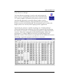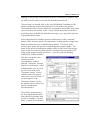
1
MRU User Manual V1.5 Series 2040 Test Systems MRU User Manual Part Number 4200-0172 Version 1.5 Series 2040 Test System Page 1 MRU User Manual V1.5 Table Of Contents Memory Replacement Unit ........................................................................... 5 MRU Block Diagram .......................................................................... 6 SOFTWARE ....................................................................................... 7 DESCRIPTION OF THE DEVELOPMENT CYCLE ..................... 7 Product Routines .................................................................... 9 Using a Product Routine ....................................................... 10 Using the Trigger Matrix with a Product Routine .................... 11 Trigger Matrix Connections .............................................................. 12 OVERVIEW OF MRUMANS PROJECT UTILITIES ............................ 14 File Menu ............................................................................. 14 Project Menu ........................................................................ 14 Tester Resources Manager ..................................................... 15 Direct Execution ................................................................... 16 Logic Analyzer ...................................................................... 17 Edit project code .................................................................. 20 Configuration ........................................................................ 20 MRU Selftest Executive ......................................................... 22 SETUP OF MRU PRIOR TO TESTING .............................................. 23 BOARD CONFIGURATION .................................................. 23 Board Number ........................................................... 23 Reset Type: ................................................................ 23 Reset Time: ............................................................... 23 CPU File: ................................................................... 24 Byte Order: ............................................................... 24 Monitor File: .............................................................. 24 Initialization File: ....................................................... 24 Active ROM Chip Select Level: .................................. 24 Boot Address: ............................................................ 25 TRIGGER MATRIX FUNCTIONS ........................................... 25 TMSetIn ..................................................................... 26 TMSetOut .................................................................. 27 ClearTM .................................................................... 28 EXTERNAL CONTROLS, CLOCKS ......................................... 30 WRITING A MONITOR PROGRAM ...................................... 31 Monitor .cpu file ..................................................... 31 MONITOR_FILE ........................................................ 33 BUS_WIDTH ............................................................. 33 BIG_ENDIAN ............................................................. 33 Page 2 Series 2040 Test System MRU User Manual V1.5 BOOT_HI_LO_FLAG ................................................. 33 EXCEPT_VEC_ADDR.................................................. 33 EXCEPT_VEC_SIZE ..................................................... 33 EXCEPT_VEC_NUM ................................................... 33 MONITOR_PARAM_ADDR ....................................... 33 INITIALIZATION_ADDR ............................................ 34 MONITOR_ADDR ..................................................... 34 MAX_INIT_SIZE ......................................................... 34 START_IO_ADDR ...................................................... 34 END_IO_ADDR ......................................................... 34 Handling exceptions ............................................................. 34 Handling special considerations ............................................ 36 Offset map for a low-boot processor ..................................... 38 Offset map for a high-boot processor .................................... 38 Description of signal area resource ........................................ 39 ADDRESS OFFSET MAP of MRU as seen from UUT processor40 Low Boot Processor: 8-bit data bus .......................... 40 High Boot Processor: 8-bit data bus .......................... 40 Communication Area ................................................. 41 Flag Byte:................................................................... 41 Exception Number Address ........................................ 42 Tester Status Register: ................................................. 42 Command Description ............................................... 43 Monitor ERROR definitions ................................................... 49 MRU Functional Calls in Visual BASIC .............................................. 49 Brief Summary ...................................................................... 49 mrBoot ...................................................................... 50 mrCall ....................................................................... 51 mrConfig ................................................................... 53 mrCopy ..................................................................... 54 mrCRC ...................................................................... 55 mrFill ......................................................................... 56 mrIn .......................................................................... 57 mrIrqEnable ............................................................... 58 mrIrqNum ................................................................. 59 mrJump ..................................................................... 60 mrLfaDisconnect........................................................ 62 mrLoad ...................................................................... 63 mrLoadImm ............................................................... 64 Series 2040 Test System Page 3 MRU User Manual V1.5 mrLoadLogicMemoryAddr ......................................... 65 mrLogicModeEnable .................................................. 66 mrLoadStackPtr ......................................................... 67 mrOut ....................................................................... 68 mrPrReset .................................................................. 69 mrRamTest ................................................................. 70 mrRead ..................................................................... 72 mrReadLFAid ............................................................. 73 mrReadLogicData ...................................................... 74 mrReceive ................................................................. 75 mrReset ..................................................................... 76 mrSelectLogicWts ...................................................... 77 mrSend ...................................................................... 78 mrSetCode ................................................................ 79 mrTMPulse ................................................................ 80 mrTMTrigEn ............................................................... 81 mrWaitTrig ................................................................. 82 mrWrite ..................................................................... 83 Maintenance ................................................................................... 84 Calibration ............................................................................ 84 Selftest .................................................................................. 84 Selftest Programs ................................................................... 84 Logic Family Adapter Test ...................................................... 85 Hardware ........................................................................................ 87 Memory Replacement Unit (MRU) ........................................ 87 Description ................................................................ 87 MRU Interconnect ..................................................... 88 Switches and jumpers ................................................ 89 Connector Pin Definitions .......................................... 90 P5 - DOS MC68331 Debugger Cable Connector ....... 92 MRU Board Part Number 0000-5356 ........................ 92 MRU Board Patchboard Interface ............................... 93 Memory Replacement Unit Interface Card ............................ 94 Description ................................................................ 94 Connector pin outs .................................................... 95 Logic Family Adapter Card (Wirewrap version shown) ........... 98 Cables ................................................................................ 103 Error Codes .............................................................................................. 109 DIGALOG MRU ERROR CODES ................................................... 110 Page 4 Series 2040 Test System MRU User Manual V1.5 Memory Replacement Unit Revision V1.5 Series 2040 Test System Page 5 MRU User Manual V1.5 MRU Block Diagram Page 6 Series 2040 Test System MRU User Manual V1.5 SOFTWARE DESCRIPTION OF THE DEVELOPMENT CYCLE The development cycle starts with determining how the UUT can be tested with the MRU system. The MRU requires the following conditions: The processor can boot from external ROM. The boot ROM chips are at least 8K bytes. The ROM access time is greater than 100 nanoseconds. Any ROM memory caching can be disabled. The boot ROM data path is less than or equal to 64 bits. Data fetches are allowed from boot ROM space. The boot ROM can be removed or disabled. The test engineer must first determine if the processor on the UUT is supported by the MRU system. If the processor is not supported, a custom monitor will need to be written. (See the section on how to write a monitor). The number of MRU boards needed must then be determined. Each 8 bits of the boot ROM data bus will require an MRU board. Next, the test engineer must determine how the MRU system will be connected to the UUT. There are generally two ways of connecting to the UUT. The first method involves removing the boot ROM chips and plugging the MRU cables into the boot ROM sockets. The second method uses a bed-of-nails fixture with wire wrapping of the connections. If the second approach is used, the boot ROM chips do not have to be removed if they can be either disabled or re-mapped to another location in the processor memory space before boot-up. In addition to the connection method, the engineer must also select the proper logic family adapter board (LFA pod) to match the logic family of the address and data bus interface chips on the UUT. Then, the test engineer configures the system using the configuration manager. When the UUT is connected to the MRU system and power is supplied to the UUT, the test engineer can use the MRUs logic analyzer to check if the system can boot. The Direct Execution mode permits the engineer to boot-up and reset the UUT as well as interactively issue commands to the monitor. Once the monitor is booted, the engineer can use the various Direct Execution mode Series 2040 Test System Page 7 MRU User Manual V1.5 commands, such as mrWrite and mrRead, to access the hardware on the UUT to verify preliminary operation. The commands used to verify the operation can be incorporated into a Visual BASIC test program to automate and to speed up hardware testing. After the engineer is satisfied with the basic operation of the UUT, the Visual Basic environment can be entered. Using Visual Basic the engineer can write test code to test the UUT. The MRU functional calls can be used with the analog functional calls to test hardware on the UUT. The following example Visual BASIC code shows the ease with which the tests can be implemented. Dim vret as Double Call PowerUUT(0, 5.0, 1.5) Call mrConfig(C:\DIGALOG\PROJECTS\EXAMPLE\MRU\MRU.INI) Call mrBoot(0) Call mrWrite(0, 1, &H1000, &HFF) Call Mux(0, 1 10) Call AMS(vret, 1, 1, 0, 0) The previous code writes a hex FF to an 8-bit Digital to Analog Converter (DAC) located on the UUT at hex address 1000. The output of the DAC is connected to channel 0 of the Relay Multiplexer (RMUX). The Mux call connects RMUX channel 0 to the Amplitude Measurement Systems (AMS) signal 1 (Sig1) with a 20 Volt range. The AMS call measures the Voltage on signal 1 and returns it in vret. The analog functional calls are fully explained in the analog programming manual. Once the test is running from Visual BASIC, the engineer can convert UUT processor intensive tests, such as memory testing and ADC calibration, into product routines. Product routines are written in the native language of the processor and can be downloaded and executed within the UUTs memory. This speeds up testing even more by eliminating the time overhead that is required for the functional calls in the Visual BASIC test program to communicate with the monitor. Instead of receiving commands one at a time from the VB test programs functional calls and returning a status reply for each commands execution, the monitor simply downloads the product routine, executes it, and returns one response. Page 8 Series 2040 Test System MRU User Manual V1.5 Product Routines Product routines are routines that are written in the native language (usually assembly language) of the processor and downloaded to the UUT for it to execute. The routines are useful for doing tests that must run at the full speed of the UUT processor, and for testing large sections of memory, which would otherwise require a lot of time just to transfer data between the tester and the monitor. The product routines can be written in C if there is accessible, tested, and sufficient read/write memory for the stack because C language routines require the use of a valid stack pointer. The MRU system itself provides approximately 2K of product routine memory space. Larger product routines will have to be downloaded into UUT read/write memory. The product routine area is provided for product routines to be downloaded into and executed from. This area is 2K locations in size, where the size of each location is determined by the bus size of the boot ROM space. For example, on an 8-bit bus, there are 2K bytes, and on a 16-bit bus, there are 2K words or 4K bytes. Sixty-four (64) locations at the top of the product routine area are reserved for passing commands and parameters to the monitor. Product routines can also be downloaded to the UUTs RAM. This allows the use of larger product routines limited only by the size of the UUT RAM. However, this memory must first be tested to assure proper code execution. In addition, the product routines can be downloaded into the monitor space thereby overwriting the monitor. This is not recommended since none of the monitor functions will be available until the monitor is reloaded and booted. Test execution results can be returned to the monitor in several ways. The product routine can place a return value in one of the processors registers. The product routine then returns back to the monitor. Next, the monitor transfers the result back to the VB functional call. The product routine also could place one or more return values in the UUTs RAM. The approach used depends on the processors architecture and the implementation of the monitor. All Digalog-written monitors are explicitly documented in this respect for the test engineer to easily write product routines that properly pass information back to the monitor upon their completion. Series 2040 Test System Page 9 MRU User Manual V1.5 Using a Product Routine The product routine is downloaded to the product routine area using mrLoad. All locations in the product routine area are acceptable for use except for the monitor communication area, which exists in the topmost 64 ocations. The product routine can be written to utilize parameters located in a noncode area of the product routine area or in an accessible area of the UUTs RAM. The VB test program uses mrLoadImm to load the parameters into the proper memory area. The product routine is executed by calling mrJump or mrCall in the test program. The mrCall causes the processor to save the address of the next monitor instruction to the stack, and then begin executing the code at the given product-routine starting-address argument. Upon completion of the routine, the processor returns back to the next monitor instruction by utilizing the address that it saved on the stack. The mrJump causes the processor to immediately begin executing the code at the given product-routine startingaddress argument. Upon completion of the routine, a jump instruction must be executed to jump to the section of the monitor that sends a return value back to the user. It then resumes waiting for the next command instruction from the MRU. All Digalog-written monitors are explicitly documented in this respect for the test engineer to easily write product routines that properly jump back into the monitor upon their completion. One advantage of the mrJump functional call over the mrCall functional call is that it can be used even if there is no UUT RAM available or before the UUT RAM has been tested because mrJump does not require a stack. To return a value to the VB test program, the product routine loads it into the UUT processor register specified in the monitor documentation for that processor. When the product routine returns to the monitor, the monitor passes the value in this UUT processor register to the mrJump functional call in the test program. The size of the return value depends on the size of the UUT processor register. If more than one value needs to be returned to the test program, the product routine can write those values to an accessible, tested area of UUT RAM. The VB test program then uses mrRead to retrieve the values from the UUT RAM area. Page 10 Series 2040 Test System MRU User Manual V1.5 The product routine returns to the monitor in one of two ways depending on how it was called. If it was called by mrJump, it must execute a jump instruction to the mrJump return address in the monitor, which was specified in the monitor documentation. If it was called by mrCall, it must execute a return from subroutine instruction to return to the monitor. The second method requires accessible, tested UUT RAM and a valid stack pointer address. Using the Trigger Matrix with a Product Routine The product routine can be synchronized with other boards in the Testhead by using the trigger matrix. Two signals are provided for connection to the trigger matrix: the UUTTrigIn signal for input from the trigger matrix and the UUTTrigOut signal for output to the trigger matrix. The UUTTrigIn line is latched and connected to bit 4 of the tester status register. This bit is high, or at logic 1, when no pulse has been received on the trigger matrix line that it is connected to. The bit goes low, or to logic 0, when a rising (logic 0 to logic 1) pulse is detected on the connected trigger matrix line. The bit remains low until the product routine reads from the ResetTM offset within the flag area. Consult the Address Offset Map of the MRU as seen from UUT processor to determine the exact address to read from for the application. The address must map to board #0 if the application has a UUT bus wider than 8 bits. The UUTTrigOut line is connected to hardware addressed at the Trigger Matrix Pulse offset within the address map. By reading from this location, a falling (logic 1 to logic 0) pulse is delivered to the connected trigger matrix line. Consult the Address Offset Map of the MRU as seen from UUT processor to determine the exact address to read from for your application. The address must map to board #0 if the application has a UUT data bus wider than 8 bits. Series 2040 Test System Page 11 MRU User Manual V1.5 Trigger Matrix Connections The MRU board has 5 output triggers and 6 input triggers that can be connected to the trigger matrix. The following are the 5 output triggers with the corresponding signal number used in the TMSetOut trigger matrix functional call. Signal N ame N umber O ut0 Signal #0 O ut1 Signal #1 FuncTrig Signal #2 ResetTrig Signal #3 UUTTrigO ut Signal #4 An active-low transition (logic 1 to logic 0) pulse is generated on either the Out0 or Out1 line by the functional call mrTMPulse and can be used to trigger some other action on another board in the Testhead configured to sense the corresponding signal. An active-low transition pulse is generated on the FuncTrig line when the auto trig mode has been enabled with the mrTMTrigEn functional call AND one of the following functional calls is executed in the test program: MRCOPY MRFILL MRREAD MRWRITE MRIN MROUT An active-low transition pulse is generated on the ResetTrig line just prior to negating the UUT reset line. The time between each of these signals will be a few microseconds. The active-low pulse on ResetTrig will occur automatically whenever the mrBoot or mrReset functional call is executed. Using this signal allows a Testhead board to be triggered whenever the UUT is booted or reset. Page 12 Series 2040 Test System MRU User Manual V1.5 An active-low transition pulse is generated on the UUTTrigOut line when a product routine executing in the UUT processor reads from the Trigger Matrix Pulse offset within the flag area of the boot ROM space. The following are the 6 input triggers with the corresponding signal number used in the TMSetIn trigger matrix functional call: Signal N ame N umber In0 Signal #0 In1 Signal #1 UUTTrigIn Signal #2 TMLogWTS Signal #3 TMLogSTRT Signal #4 TMLogSTO P Signal #5 When the MRU board detects a rising signal edge on the In0 or In1 line, it is latched and can be checked for with the functional call mrWaitTrig. The mrWaitTrig functional call then clears the latch before it returns. If a pulse has been latched before mrWaitTrig is called or its TimeOut parameter is zero, it will clear the latch and return immediately. The UUTTrigIn line is connected to the tester status register, which can be read by a product routine executing in the UUT processor. This allows a product routine to wait for some trigger from another Testhead board. The address of the tester status register is given in the Address Offset Map of MRU as seen from UUT Processor section of this manual. The TMLogWTS line is connected to the logic analyzer memory and is used as a clock to capture the state of the address, control, and data lines connected to the UUT boot ROM socket. The TMLogSTRT and TMLogSTOP lines are connected to the enable logic of the logic analyzer memory and are used to start and stop capturing of the address, control, and data lines connected to the UUT boot ROM socket. Series 2040 Test System Page 13 MRU User Manual V1.5 OVERVIEW OF MRUMANS PROJECT UTILITIES The MRUMAN program provides a starting point for project development. It also serves as a launch pad for the Tester Resources Manager, the Direct Execution mode, the MRU Logic Analyzer utility, the MRU Configuration editor, the Visual Basic program development environment, and the MRU Selftest Executive. When the program is executed, the screen to the right is displayed showing the projects available in the Digalog\Projects directory. If none of the projects in this directory is a MRU project, an appropriate message box is displayed. File Menu The MRUMAN File menu contains selections to Create a project, Delete a project, Reread the project list, or Exit the program. An existing project can only be selected by clicking on it with the mouse. If the project directory selected does not contain a MRU project, a message box is displayed prompting the user to create one. For the purposes of this discussion, a project named Example could be created by selecting Create from the File menu and entering the name Example in the resulting inputbox. This also creates a subdirectory called Digalog\Projects\Example\MRU where MRU project specific files are stored. Project Menu Once the project is selected or created, it must be properly configured. All project specific information can be entered or edited using options from the Project menu. These options include Tester Resources, Direct execution, MRU Logic Analyzer, Edit project code, Configuration, and Selftest. Page 14 Series 2040 Test System MRU User Manual V1.5 Tester Resources Manager The Tester Resource Manager is used to track and manage the tester resources including all the boards in the Testhead and the UUT power supplies. Information about these resources can be automatically generated or manually defined, and are used to generate a Patchboard Interface Map and define the pin locations of these resources at the Patchboard. This information can be saved to the Registry and can be used by other Digalog Systems applications. Specifically, the software is capable of printing out a Patchboard Map containing Patchboard pin mnemonics by either automatically interrogating the tester for its resources, or by asking the programmer to define the testers resources. When the configuration is performed manually, it allows the programmer to configure additional resources beyond what the tester physically contains. In this manner, a programmer has the additional resources and dialogs to generate programs and fixtures for any tester. Series 2040 Test System Page 15 MRU User Manual V1.5 Direct Execution Direct Located under the Project menu, The Direct execution utility provides direct execution of MRU functional calls, functional call Execution parameter list examples, drop down menu access to functional calls and macro definition and execution capabilities. When invoked by MRUMAN, Direct Execution accepts the path to the currently selected MRU project. All macros developed, will then be saved in the projects MRU subdirectory. The Direct Execution mode enables the user to interactively execute any MRU functional call. This mode provides direct, immediate feedback to the user as an aid in troubleshooting the hardware interfacing and in streamlining the building process of each test program. After a MRU functional call is entered into the single-line text entry box at the bottom of the screen, the results of its execution appear in the upper portion of the screen (following the output of the previously executed functional call) for the user to easily follow. This history code can then be printed out to use as a reference for code development later on in the Visual BASIC programming environment. It also features the ability to create and process macros, which are short, user-definable names used to represent the MRU functional calls and includes their parameter lists. These macros can be saved to a file and later retrieved. Page 16 Series 2040 Test System MRU User Manual V1.5 Under the File menu option, the choices for loading and saving macro files, for printing out the history code, and for terminating this application are available. Under the Edit menu option, the choices for removing, copying, inserting, and erasing selected sections of the entered functional call are available as well as the options to create, delete, and clear all macros. The Subroutine menu option lists all of the MRU functional calls to choose from and presents the parameter list usage below the text field once a call has been chosen from the list. The user can also enter the functional call via the keyboard, but no parameter list information will be provided. In this case, the section on functional calls in this manual will have to be consulted. The Macro menu option lists the available macros to choose from for immediate execution. Logic Analyzer The Logic Analyzer utility graphically displays the signal levels that were read by an MRU boards logic analyzer circuitry and saved to a log file. If the system is configured for multiple MRU boards, the signal levels from each MRU board are written to the same log file. Since the MRU Logic Analyzer utility can only display eight data lines at a time (in addition to the address and control lines), to load a multiple-MRU-board log file, it will invoke itself automatically and repeatedly to show all of the data Series 2040 Test System Page 17 MRU User Manual V1.5 lines. For example, when a 16-bit product is monitored, there will be two MRU Logic Analyzer utilities with one displaying D0-D7 and the other, D8-D15. The address and control signals display the same values in each utility invocation. The control signals that are monitored consist of: Name Description ROM CS The ROM chip select ROM OE The ROM output enable P R ES ET Product Reset (controlled by MRU) PW T S Product write strobe to write to MRU RAM Ex t. LogWTS Ex ternal Logic Analyzer write strobe Ex t. LogStart Ex ternal logic analyzer enable Ex t. LogStop Ex ternal logic analyzer disable This utility also features golden log file comparison and hexadecimal representation of the data and address lines. It also continuously updates the information fields displaying the signal name, the signal levels, and the time index to reflect the current position of the mouse pointer within each log file. The actions listed under the File menu option operate on the user-selectable sample log file, which is plotted in red upon being loaded. The actions listed under the Golden menu option operate on the user-selectable Page 18 Series 2040 Test System MRU User Manual V1.5 golden log file, which is plotted in blue upon being loaded. The golden log file, which contains the signal behavior of a properly working product, can be any log file (just like the sample log file) and will overlay the sample log file when loaded. Any discrepancies between the two log files will then appear in red and be easily noticed. The Help menu option provides access to the help file via its Contents and Search for Help on... submenu items. The Timebase field contains the timebase used for logging this data and is extracted from the log file. Various timebases accommodated by the MRU board are asynchronous clocks periods of 20, 40, 80, 100, 200, and 400 nano-seconds; product bus cycles; and an external signal. The Timebase field will contain the clock period value, the phrase Bus Cycle, or the word Unknown, respectively. The Signal field contains the name of the signal whose waveform the mouse pointer is currently positioned over. Depending on the timebase selected, the Time field contains the time division index, the bus cycle index, or the log sample index of the mouse pointers current position. The Sample data and Sample address fields contain the hexadecimal values of the data and address signals, respectively, in the sample file whose timebase index the mouse pointer is currently positioned over. The Golden data and Golden address fields contain the hexadecimal values of the data and address signals, respectively, in the golden file whose timebase index the mouse pointer is currently positioned over. The Cycles to Shift field is used to specify how many cycles the sample data or golden data is to be shifted when the << or >> command button associated with the Cycles to Shift field is selected. The need to shift the sample data or golden data occurs when the two batches of samples do not start on the same cycle. By shifting one of the sample sets, both of the sample sets can be aligned to the same cycle. When either of the sample sets are shifted up (to the right), the invalid signal state shown on the leftmost portion of the Logic Analyzer will not show up as being high or low. Instead it will be Series 2040 Test System Page 19 MRU User Manual V1.5 displayed as being filled in. The signal state is invalid because it is not an actual sample taken. The Block information and manipulation controls are located below the Time field. A block consists of 512 samples of the monitored signals. Incrementing up and down through the blocks is performed using the >> and << command buttons, respectively. The block index and the corresponding timebase index range for the currently visible waveform are also displayed. The Logic Analyzer utility can be used to troubleshoot the boot-up sequence of an uncommunicative product by enabling one of the asynchronous clock sources to capture the various signal states after reset. The results can then be viewed to check for various anomalies, such as short-circuited or stuck-at signal conditions, illegal opcodes, and incorrect branching destinations. Edit project code When this option is selected from the MRUMAN menu, the program opens Visual BASIC. It will open the .vbp file with the same name as the project (in this case it will open example.vbp) in the Digalog\Projects\Example\MRU directory (example project). If no .vbp file exists in that directory, Visual BASIC opens the standard blank Project1.vbp. When VB code for the Example project is stored, it should also be stored in this directory. Configuration The MRU Configuration editor manages the necessary information describing the products configuration and the various files needed to control and interact with the product during testing. The first step to create a configuration for the current project is to double-click on the text field labeled CPU File and select the CPU configuration file that matches your product. This file describes the possible bus width options, specifies the monitor and default initialization files, and alerts the user to set up any additional or special CPU-related considerations, such as the address location of a particular relocatable CPU register that the monitor might use. The monitor file is a boot-up program that has been written in the native Page 20 Series 2040 Test System MRU User Manual V1.5 language of the product and performs whatever commands are given to it by the MRU board in order to execute the desired functional call. The next step is to double-click on the text field labeled Initialization File and then select the monitor initialization file to be used for this project. The initialization file contains code that is executed by the product after being reset, but before the monitor is run. It may include instructions to disable a watchdog timer, to disable the maskable interrupts, or to specify the behavior of programmable I/O pins. If the selected monitor handles special considerations, hit the command button called Monitor Specific Considerations to bring up the configuration editor that allows the user to initialize these options. The writer of the monitor must specify the special considerations the monitor handles. The name of the special considerations and the MRU boards Boot RAM storage space (in bytes) needed for these special considerations are entered by the writer of the monitor into the processors .cpu file under the heading MONITOR_PARAM_NAMES. This data is read when the Monitor Specific Considerations editor is selected. When the Monitor Specific Considerations editor is displayed the user can click on one of the items in the Parameter Names section and then enter the desired value in the text box below. If no items appear in the Parameter Names section the monitor does not have any special considerations associated with it. The polarity and duration of the reset signal that the MRU board drives the product with can be set using the Product Reset controls. If the duration Series 2040 Test System Page 21 MRU User Manual V1.5 is not known, the Learn Valid Reset option can be executed. This utility will determine the minimum reset duration needed (from 500 uS to 500 mS). Next the active level of the UUTs ROM chip select level can be selected in the Active ROM Chip Select Level section. There are two available options: active high and active low. It should be set to the same level as UUT processors ROM chip select level. This needs to be initialized so the LFA can be properly set up to correctly pass read and write data from the UUT to the MRU board. The Byte Order section shows which MRU board number is assigned to which UUT boot ROM data byte. It is used for informational purposes only. This information can not be changed by the user. Due to software limitations, the least significant data byte is always assigned to MRU board #0. Finally, the boot address is entered. This is only used for cases where the boot space on a low-boot processor has been re-mapped to another location. The location of the re-mapped boot space is needed so the exception vectors within the monitor can be changed to their new location. If a high-boot processor is configured or the boot space is not re-mapped, this field should be zero. If the product contains more than one processor, then the Processors field will have to be incremented. When this field is incremented, another processor tab will appear next to the first one (Proc 1). The new processor tab will then have to be selected, and the configuration data for the new processor will have to be entered. When all of the information has been entered, the configuration file should be saved using either the Save or Save As... operation under the File menu option. MRU Selftest Executive The MRU Selftest Executive provides the means to functionally test all of the MRU boards in the Testhead. For a description of the Selftest programs, see the Selftest Programs section of this manual. Page 22 Series 2040 Test System MRU User Manual V1.5 SETUP OF MRU PRIOR TO TESTING BOARD CONFIGURATION Board Number Each Memory Replacement Unit (MRU) Testhead board is responsible for 8bits of data-bus ROM emulation on a product. Therefore, if the product contains a sixteen-bit processor, the tester requirements would be two MRU boards. Likewise, a thirty-two bit processor would require four MRU boards. Each MRU board has an eight-switch dip package that is used to assign this board to a UUT ROM data byte and which processor group it is assigned to. The processor group is needed when one UUT has more than one processor on it. The lower nibble is used to distinguish which data byte it is assigned to and the upper nibble is used to distinguish which processor group it is assigned to. Within each processor group, MRU board number 0 must be assigned to the least significant ROM data byte. The assignment of the processor group number is up to the user. Example: SW1- 8 SW1- 7 SW1- 6 SW1- 5 SW1- 4 SW1- 3 SW1- 2 SW1- 1 0 0 0 1 0 0 1 0 SW1-1SW1-2SW1-3SW1-4SW1-5SW1-6SW1-7SW1-8 This configuration would signify board two (zero inclusive) of group one (zero inclusive) or the MRU board responsible for data bits sixteen through twentythree on the second processor. All configuration concerns listed below are contained in a file named mru.ini located in the Projects\MRU directory. This information is entered through the MRU Configuration Editor. Each configuration concern is also available for each processor when multiple processors are present. Reset Type: The reset type specifies the reset signal as active-high or active-low. This signal is generated on the MRU-controlled LFA pod board. Reset Time: The reset time specifies the duration of the reset signal that is generated on the MRU-controlled LFA pod board. Series 2040 Test System Page 23 MRU User Manual V1.5 The bus width specifies the configuration of the MRU boards required to emulate the ROM devices. For example, if a single 16-bit processor is selected, the data bus width is sixteen bits and therefore creates a system requirement of two MRU boards. Software determines that the two MRU boards are for the same processor and executes accordingly. This value is part of the .cpu file and cannot be edited from this dialog. CPU File: This file contains all CPU-specific configuration concerns, such as bus width, high or low boot processor, name of the monitor file, etc.. Byte Order: The byte order is the significance arrangement of the CPU data bus. For example, the Motorola 680xx family of processors uses Big Endian (MSB at lowest address) while the Intel 80x86 family uses Little Endian (LSB at lowest address). It is used for informational purposes only. This information can not be changed by the user. Due to software limitations, the least significant data byte is always assigned to MRU board #0. Monitor File: This file is downloaded into the ROM space of the product (RAM on the MRU board) and is responsible for accepting and acting upon commands given to it to allow the test engineer to fully interact with and test the product. The monitor file to be used can not be changed by the user. It is specified within the CPU file. The CPU file is generated by the writer of the monitor and the two files must go together. Initialization File: This project-specific file contains processor setup routines that are executed by the processor immediately following its reset mode, but prior to execution of the monitor program. Active ROM Chip Select Level: Used to select the active state of the UUTs ROM chip select signal. This needs to be initialized so the LFA can be properly set up to correctly pass read and write data from the UUT to the MRU board. Page 24 Series 2040 Test System MRU User Manual V1.5 Boot Address: This is only used for cases where the boot space on a low-boot processor has been re-mapped to another location. The location of the re-mapped boot space is needed so the exception vectors in the monitor can be changed to their new location. If a high-boot processor is configured or the boot space is not re-mapped, this field should be zero. TRIGGER MATRIX FUNCTIONS The following pages contain the description of the functional calls that are used with the trigger matrix feature located on the MRU card. Syntax for Visual BASIC is provided. Series 2040 Test System Page 25 MRU User Manual V1.5 TMSetIn The TMSetIn function is used to make or break Trigger Matrix connections to the inputs of boards containing Trigger Matrix hardware. Due to hardware restrictions, an input to a board cannot be connected to more than one Trigger Matrix channel at a time. If the selected input signal is already connected to a different TMBus channel, the connection will be broken. Passing a negative number for the Channel parameter will break the connection between the signal selected and the Trigger Matrix Bus. The signal is selected by crossreferencing the signal name to the number that represents it for that particular board type and then inserting it into the Sig parameter. Visual BASIC Declaration: Public Sub TMSetIn(ByVal Channel As Integer, ByVal Slot As Integer, ByVal Sig As Integer) Call TMSetIn (Channel, Slot, Sig) Where: Channel = 0 to 7. TMBus channel to connect/disconnect to/ from. Slot = 1 to 23. The Testhead slot containing the board. Sig = = = = = 0 1 2 3 4 Out 0. Out 1. FuncTrig. ResetTrig. UUTTrigOut. These are the only Trigger Matrix input signals available on the MRU Board. EXAMPLES: Const BREAKIT = -5 Channel = 5 Slot = 22 Sig = 0 Call TMSetIn(Channel, Slot, Sig) ............................................................. connects input signal .............................................................................. 0 of board in slot 22 to TMBus channel 5. Call TMSetIn(BREAKIT, Slot, Sig) ....................... disconnects input signal 0 of board in slot 22 .......................................................................................................... from TMBus channel 5. Page 26 Series 2040 Test System MRU User Manual V1.5 TMSetOut The TMSetOut function is used to make or break Trigger Matrix connections to the outputs of boards containing Trigger Matrix hardware. To avoid conflicting sources, no two outputs from Testhead boards will be allowed to drive a single Trigger Matrix Bus channel at one time. If the selected input signal is already connected to a different TMBus channel, the connection will be broken. Passing a negative number for the Channel parameter will break the connection between the signal selected and the Trigger Matrix Bus. The signal is selected by cross-referencing the signal name to the number that represents it for that particular board type and then inserting it into the Sig parameter. Visual BASIC Declaration: Public Sub TMSetOut(ByVal Channel As Integer, ByVal Slot As Integer, ByVal Sig As Integer) Call TMSetOut(Channel, Slot, Sig) Where: Channel = 0 to 7. TMBus channel to connect/disconnect to/ from. Slot = 1 to 23. The Testhead slot containing the board. Sig = = = = = = 0 1 2 3 4 5 In0Trig. In1Trig. UUTTrigIn. TMLogWTS. TMLogSTRT. TMLogSTOP. These are the only Trigger Matrix output signals available on the MRU Board. EXAMPLES: Const BREAKIT = -5 Channel = 5 Slot = 22 Sig = 0 Call TMSetOut(Channel, Slot, Sig) ...................... connects outputsignal 0 of board in slot 22 .............................................................................................................. to TMBus channel 5. Call TMSetOut(BREAKIT, Slot, Sig) ........ disconnects output signal 0 of board in slot 22 from .................................................................................................................. TMBus channel 5. Series 2040 Test System Page 27 MRU User Manual V1.5 ClearTM ClearTM breaks all input and output connections of every Testhead board from a specific Trigger Matrix Bus channel. This function works well to clear the way for programming Trigger Matrix connections to a TMBus channel of unknown status. Visual BASIC Declaration: Public Sub ClearTM(ByVal Channel As Integer) Call ClearTM(Channel) Where: Channel = 0 to 7. The TMBus channel to be cleared. EXAMPLES: Dim Channel As Integer Channel = 0 Call ClearTM(Channel) ........................................ clear all connections to TMBus channel 0. Page 28 Series 2040 Test System MRU User Manual V1.5 Trigger matrix interface controls and clocks Out 0 - software-generated trigger output created by MRU firmware from functional call mrTMPulse(). Out 1 - software-generated trigger output created by MRU firmware from functional call mrTMPulse(). FuncTrig - software-generated trigger output created by MRU firmware during execution of certain functional calls. ResetTrig - software-generated trigger output created by MRU firmware during product reset. UUTTrigOut - product generated trigger output lasting one UUT bus cycle. In 0 - software-monitored trigger input via functional call mrWaitTrig(). In 1 - software-monitored trigger input via functional call mrWaitTrig(). UUTTrigIn - UUT-monitored input trigger. TMLogWTS - Trigger Matrix input signal used to capture logic analyzer data samples. TMLogSTRT - Trigger Matrix input signal used to arm the logic analyzer. TMLogSTOP - Trigger Matrix input signal used to disarm the logic analyzer. Series 2040 Test System Page 29 MRU User Manual V1.5 EXTERNAL CONTROLS, CLOCKS LFA Pod interface controls and clocks UD[x] - UUT data lines zero to seven, eight to fifteen, sixteen to twenty-three, etc., dependent on MRU board number. UA[x] - UUT address lines zero to thirteen. UROMVCC - product VCC monitoring signal. UROMCS* - product ROM chip select signal monitored and used for emulation control. UBUSQUAL* - product signal logically ord with UROMCS* to define the valid and inactive regions of a bus cycle. UROMOE* - product ROM output enable monitored and used for emulation control. URESET - product ROM reset signal generated by MRU and used for emulation control. UWTS* - product ROM write strobe signal monitored and used for emulation control. UXLOGWTS* - externally generated write strobe used to capture logic analyzer data samples. UXLOGSTRT* - externally generated software-generated signal used to arm logic analyzer. UXLOGSTOP* - externally generated software-generated signal used to disarm logic analyzer. GND - product ground used to match LFA pod ground and to shield signals in twisted-pair wiring. Page 30 Series 2040 Test System MRU User Manual V1.5 WRITING A MONITOR PROGRAM The monitor program accepts commands to read and write any location in the UUT processors address map. The test engineer uses Visual BASIC to send commands to the MRU board. The MRU breaks the command into lower level commands to be executed by the monitor. This allows the UUT to be tested without having to program test routines in the native language of the UUTs processor. The MRU also accepts commands to download data to any space in the UUTs address map. This data could be machine language product routines which the monitor can be instructed to execute. The monitor will be downloaded to the memory location given by the MONITOR_ADDR entry in the projects CPU file. This location is specified by the author of the monitor program. When the UUT boots up, the first code that is executed is the initialization file. A default initialization file is supplied by Digalog. The test engineer can add code to this file that is specific to the UUT. The initialization code is used to set up registers, enable/disable watchdogs, and anything else that must be setup either due to time or order-of-execution restrictions. This code might also be needed to setup the UUT to be able to execute the monitor from the MRU board. The initialization code is always executed prior to the monitor even if the only function of the initialization code is to jump to the monitor. The initialization file will be downloaded to the memory location given by the INITIALIZATION_ADDR entry in the projects CPU file . This location is also specified by the author of the monitor program. Monitor .cpu file Each monitor must be accompanied with a second file. This file must have a .cpu file name extension. The .cpu file will contain configuration type information specific to the processor the monitor is written for. The .cpu file is read when the mrConfig functional call is executed. The information contained in the .cpu file is then used to setup the MRU hardware and software for the processor it was created for. The listing on the next page shows the elements that must be in the file with example settings for each element. Following the listing is a description of each element. The section titled [GENERAL] must be in every .cpu file. All of the elements must be initialized except the two dealing with a processors I/O space. These two elements are only valid for processors that have an I/O space. Series 2040 Test System Page 31 MRU User Manual V1.5 The section titled [MONITOR_PARAM_NAMES] is optional. This section deals with processor options (see the Special Considerations option in the configuration editor) that are not dealt with in the [GENERAL] section of the .cpu file or are not part of the configuration editor. An example of an option that would have to be handled in this section is the location of a processorss registers if they can be relocated within the processors memory map. First, the writer of the monitor assigns a name to each element they place under the [MONITOR_PARAM_NAMES] section. Then each element is initialized to the number of bytes needed to be reserved in the MRU boot RAM to store the elements value (the value will be assigned by the user through the Special Considerations option of the Configuration Editor). In the example below, the special consideration called REGISTER_VECTOR is assigned to handle a maximum of two bytes. The user can then enter a maximum of two bytes for this option in the Special Considerations option. The two bytes entered by the user would be the address where their product has the processors registers located. The Special Consideration data is written to the MRUs boot RAM address given by MONITOR_PARAM_ADDR when the mrConfig functional call is executed. The monitor can then read this data at the given MRU boot RAM address. [GENERAL] MONITOR_FILE=c:\digalog\include\mon68020.bin BUS_WIDTH=1 BIG_ENDIAN = TRUE BOOT_HI_LO_FLAG=LOW EXCEPT_VEC_ADDR=000 EXCEPT_VEC_SIZE=4 EXCEPT_VEC_NUM=256 MONITOR_PARAM_ADDR=800 INITIALIZATION_ADDR=400 MONITOR_ADDR=000 MAX_INIT_SIZE=40 START_IO_ADDR= END_IO_ADDR= [MONITOR_PARAM_NAMES] REGISTER_VECTOR=2 Page 32 Series 2040 Test System MRU User Manual V1.5 MONITOR_FILE Specifies the full path to the monitor file associated with this .cpu file. The monitors are usually kept in the ..\digalog\include directory. BUS_WIDTH Specifies the width, in bytes, of the boot ROMs data bus for this processor. The valid numbers are 1, 2, 4, and 8. BIG_ENDIAN Specifies if this processor uses big-endian (i.e. Motorola) or little-endian (i.e. Intel) format. For a big-endian processor this element is set to TRUE and for a little-endian processor this element is set to FALSE. BOOT_HI_LO_FLAG Specifies if this processor is a high or low boot. For a high boot processor the valid entry is HIGH and for a low boot processor the valid entry is LOW. EXCEPT_VEC_ADDR Specifies the address location within the MRUs 4K boot space of the first exception vector. This element will only be used by projects with low boot processors that have had their boot space re-mapped. If the boot space is remapped the exception vectors will have to be rewritten to correspond to the new location. EXCEPT_VEC_SIZE Specifies the size, in bytes, of each exception vector. This information is needed so the software knows how to rewrite the exception vectors to the MRUs boot space for the various combinations of exception vector bytes and number of MRU boards for a given project. EXCEPT_VEC_NUM Specifies the number of exception vectors for this processor. MONITOR_PARAM_ADDR Specifies the address where the software will automatically place the monitors special consideration information within the MRUs boot space. This is one of three boot space addresses that must be specified by the writer of the monitor. The other two are INITIALIZATION_ADDR and MONITOR_ADDR. The addresses were to load these three items must be given by the writer of the Series 2040 Test System Page 33 MRU User Manual V1.5 monitor because the monitor location were a product routine will jump to after a mrJump command must also be given by the writer of the monitor. And since this location can not change, the location of the monitor must not change. INITIALIZATION_ADDR Specifies the address where the software will automatically place the monitors initialization code within the MRUs boot space. MONITOR_ADDR Specifies the address where the software will automatically place the monitors code within the MRUs boot space. MAX_INIT_SIZE Specifies the maximum size for the initialization code. Since the writer of the monitor maps where the monitor, initialization code, and special consideration information goes and since the user can add to the initialization code, the maximum space this code can take in the boot space must be specified so these three items do not overwrite each other. START_IO_ADDR Specifies the starting I/O space address for the processor. This element is only valid for processors that have an I/O space. END_IO_ADDR Specifies the ending I/O space address for the processor. This element is only valid for processors that have an I/O space. Handling exceptions The monitor must be written so it can handle exceptions. Fatal and nonfatal interrupt service routines (ISRs) need to be handled differently. The nonfatal ISRs first need to check if the UUTs stack pointer has been initialized (by the mrLoadStackPtr function). If the stack has been initialized, bit #1 of the Flag Byte in the Communication Area will be set. If the stack has not been initialized (or there is no UUT RAM), the ISR cannot return by way of a return from interrupt instruction because there is no valid return address. In this case, the ISR should just jump to the monitors command loop and wait for the next instruction. If the stack has been initialized, the nonfatal ISR needs to Page 34 Series 2040 Test System MRU User Manual V1.5 check if interrupts are expected (by the mrIrqEnable function). ISRs are expected if bit #0 of the Flag Byte in the Communication Area is set. If they are not expected the return from interrupt instruction should be executed. If interrupts are expected, the exception number needs to be stored at the UUT RAM address that is specified in the exception address location in the Communication Area (see the description of the Communication Area below). The exception number can then later be retrieved by the mrIrqNum functional call. Once the exception number has been stored, the return from interrupt instruction can be executed to resume monitor or product routine execution. Fatal interrupts need to be handled differently. Since the state of the UUT cannot be guaranteed after a fatal interrupt, the user should be notified of the fatal interrupt by returning the monitors ERR_EXCEPTION error. If the UUTs stack has been initialized, the fatal ISR can save the interrupt number just like in nonfatal ISR handling before returning the exception error. Series 2040 Test System Page 35 MRU User Manual V1.5 Handling special considerations Since the configuration editor cannot account for every configurable option of every existing and future processor, the monitor must be able to handle these special options. These options are defined by the writer of the monitor and entered into the .cpu file for the processor the monitor is being written for. The first value that needs to be defined and entered is the Boot RAM address where the MRU firmware will place the parameters for the special considerations. This address is assigned to the MONITOR_PARAM_ADDR entry within the [GENERAL] section of the .cpu file. Care must be taken so the required data space for these parameters is not placed within the initialization code or the monitor itself. Next to be entered is the name of each option and the number of bytes that each will occupy in the Boot RAM (of MRU board #0 only). The parameter names are entered under the section titled [MONITOR_PARAM_NAMES] in the .cpu file. This is an example of the Special Consideration additions needed to be made to the .cpu file: [GENERAL] . MONITOR_PARAM_ADDR=0x3B00 . . [MONITOR_PARAM_NAMES] REGISTER_VECTOR=2 RAM_VECTOR=2 . In this example, four bytes (2 bytes for each special consideration) are reserved at address 0x3B00 in the boot RAM space. Therefore, the monitor would read two bytes at address 0x3B00 to get the REGISTER_VECTOR and two bytes at address 0x3B02 to get the RAM_VECTOR. The monitor must be able to interpret the data generated by the Special Considerations section of the configuration editor. An example of a special consideration would be a processor that has a watchdog timer that cannot be disabled by the initialization code because the timers address resides in a relocatable register. In this case the monitor must handle the resetting of the watchdog before it times out. Therefore, the monitor code must be informed Page 36 Series 2040 Test System MRU User Manual V1.5 by the user as to where the register is located so that it can disable the watch-dog timer on boot-up. This can be accomplished by placing the address of the relocatable register in the boot RAM space for the monitor to fetch at the proper time. The address of the relocatable register is automatically placed in the boot RAM space by the mrBoot functional call. However, the value of the relocatable register must be specified by the user from within the Monitor Specific Considerations editor which is part of the MRU Configuration Editor. When the configuration is saved the value of the relocatable register is saved to this projects mru.ini file. Which is then read by the mrConfig functional call and then available to the mrBoot functional call. NOTE: To properly fetch the data on a UUT with a 16-bit data bus, the monitor needs to fetch each data byte separately using a byte-wide operation and then concantenate the bytes together to form the proper value. Thus, the first byte is located at address (MONITOR_PARAM_ADDR) and the second at (MONITOR_PARAM_ADDR +2). For a 32-bit data bus, each byte is located 4 addresses away from the previous one. The resources available to the monitor consist of the processors registers, 4K-location boot ROM space, (2K-64)-location product routine area, 256-location signal area resource, and a 64-location communication area. All sizes are given in locations, which is bytes if the data bus width is 8 bits, words if the data bus width is 16 bits, or long words if the data bus width is 32 bits. NOTE: Even though the communication area can be byte-wide, word-wide, or longword-wide, depending on the data bus width, its data is stored contiguously in the boot RAM of MRU board #0 only. To fetch a word using a word-wide data bus requires two byte wide read operations specifying two addresses not adjacent to each other, but having a difference of two. For a longword-wide architecture, adjacent data bytes in the communication area have addresses that differ by four. Thus, the monitor must take the CPUs data bus architecture into account when retrieving words and long words from the communication area. Series 2040 Test System Page 37 MRU User Manual V1.5 Offset map for a low-boot processor O ffset Size Section 0 4K Monitor Area 0x1000 2K Product Routine Area 0x1800 256 Signal Area 0x1900 256 Flag Area 0x1A00 1K MRU Status Register 0x1FFF End of 8K region Offset map for a high-boot processor O ffset Size Section 0 2K Product Routine Area 0x0800 256 Signal Area 0x0900 256 Flag Area 0x0A00 1K MRU Status Register 0x1000 4K Monitor Program 0x1FFF End of 8K Region NOTE: The offset of 0 is actually 8K below the top of memory. The MRU board maps into an 8K-location region of the boot ROM space. The 8K region is located either at the top of memory or at the bottom depending on whether the UUT processor boots from high or low memory. The monitor has a 4K-location space allocated to it out of the 8K region. This 4K space holds the initialization code, the monitor code, various startup parameters, and the vector table. The remaining 4K space of the 8K region is mapped into a 2K-location product routine area, a 256-location signal area resource, a 256-location flag area, and an MRU status register. The MRU uses the top 64 address locations in the product routine area to pass commands and parameters to the monitor. The Page 38 Series 2040 Test System MRU User Manual V1.5 256-location signal area resource is used by the monitor to pass values back to the firmware. The 256-location flag area is used to trigger events on the trigger matrix bus and signal errors to the MRU. The MRU status register is used to inform the monitor that a command is in the communication area and that the MRU has released its control of the product routine area for the monitor to now be able to fetch its next instruction. Description of signal area resource The purpose of the signal area is to provide a communication path from the monitor back to the MRU. Because the monitor only has readable access to the ROM space, it cannot write data to be returned to the MRU. Thus, another method is used, the signal area resource. The signal area resource is only available on MRU board #0. Board #0 is always connected to the least significant byte of the UUT data bus. The MRU loads the 256 locations of the signal area resource with the signal values 0-255 (in sequential order). The monitor or product routines can use this section to communicate data back to the MRU. To use the signal area resource (lookup table), the executing code performs a read access at the location containing the number that it wants to transfer back to the MRU. The value at that location is latched for the MRU to read, and a flag is set in the flag area to notify the MRU that a signal value has been latched. Addressing of the signal area locations must take into account the width of the data bus in the same way as the communication area must be addressed. Series 2040 Test System Page 39 MRU User Manual V1.5 ADDRESS OFFSET MAP of MRU as seen from UUT processor Low Boot Processor: 8-bit data bus Start End Description Attributes 0x0000 0x0FFF Monitor Program Area Read O nly 0x1000 0x17BF Product Routine Area Read O nly 0x17C0 0x17FF Communication Area Read O nly 0x1800 0x18FF Signal Area Read O nly 0x1901 Trigger Matrix Pulse Read O nly 0x1904 Reset of TM Input Read O nly 0x1908 Error Flag Read O nly 0x1A00 Tester Status Register Read O nly 0x1A01 Enable Logic Analyzer Mode Read O nly 0x1A02 Disable Logic Analyzer Mode Read O nly High Boot Processor: 8-bit data bus Start End Description Attributes 0x0000 0x07BF Product Routine Area Read O nly 0x07C0 0x07FF Communication Area Read O nly 0x0800 0x08FF Signal Area Read O nly 0x0901 Trigger Matrix Pulse Read O nly 0x0904 Reset of TM Input Read O nly 0x0908 Error Flag Read O nly 0x0A00 Tester Status Register Read O nly 0x0A01 Enable Logic Analyzer Mode Read O nly 0x0A02 Disable Logic Analyzer Mode Read O nly Monitor Program Area Read O nly 0x1000 0x1FFF NOTE: The offset of 0 is actually 8K below the top of memory. Use of the Error Flag offset signals the MRU that an error has occurred and that it should request the error code number from the monitor. The flag is generated by a read access within the flag area with address bit A7 asserted high on MRU board #0. Page 40 Series 2040 Test System MRU User Manual V1.5 Communication Area Located at offset 0x7C0 above the product Routine Area, the following parameter locations are defined as indicated: Data Type Primary Address O ffset 0 Secondary Address 4 Data Type Offset Data Value #1 8 Data Value #2 16 Data Value #3 24 Data Value #4 32 Data Value #5 40 Data Value #6 48 Command Number 56 Flag Byte 57 Exception Address 58 Flag Byte: Bit 0: IRQ Enabled Flag 0 = interrupt (exception) number capturing disabled 1 = interrupt (exception) number capturing enabled This bit is used by the interrupt service routines to determine whether to save or discard the exception number when an exception occurs. This bit will only be asserted by the firmware if a valid stack pointer has already been loaded. Bit 1: Stack Enabled Flag 0 = invalid stack pointer 1 = valid stack pointer This bit is used to verify proper use of the mrCall functional call, to check if a valid stack exists, and to signal what action to take when servicing an interrupt. Series 2040 Test System Page 41 MRU User Manual V1.5 Exception Number Address The initial stack pointer value is written here by the MRU when the Load Stack Pointer command is given. The monitor reserves this initial stack location for storage of an exception number if one should occur. The stack then actually starts one location above (or below depending on the stacks direction) from the initial stack pointer. All information in the communication area conforms to the byte-ordering of the UUT processor. Addressing of the communication area by the monitor must take into account the bus width. To address Data Value #1 on a single byte machine, an offset of seven bytes would be added to the Data Value #1 location. Tester Status Register: Bits 0-2: Unassigned These bits may be used by a product routine to receive commands from the test program. Bit 3: Command ready Flag 0 = No command ready 1 = Command ready This bit is used to signal the monitor program that a command has been loaded into the communication area. Bit 4: Trigger Matrix In 0 = Pulse received 1 = No pulse received This bit is used to signal the UUT that a pulse was received on the trigger matrix bus. Bit 5: Product Routine Area Access Flag 0 = UUT does not have access 1 = UUT has access This bit is used to determine if the UUT has access to the product routine and communication area. The MRU places the command number and parameters in the communication area and then switches access to the UUT. If the monitor attempts to access the area without Page 42 Series 2040 Test System MRU User Manual V1.5 permission, it will not retrieve the correct data. Bit 6: Monitor Program Space Access Flag (MRU Boot RAM) 0 = UUT does not have access 1 = UUT has access This bit is used to determine if the UUT can access the monitor program area RAM on the MRU board. The MRU loads the monitor, switches access to the UUT, and resets the UUT to boot the monitor. Bit 7: Signal Ready Flag 0 = MRU has not read the latched signal value 1 = MRU has read the latched signal value This bit is used to determine if the MRU has read the previous signal value. Command Description The monitor program must handle the following set of commands. Any commands that are unsupported for the processor must return the error code ERR_UNSUP_COMMAND. Command Command Read Description Description Reads a location in the UUT memory space. Write Writes a location in the UUT memory space. C opy Copy one section of UUT memory to another. Fill Fill an area of UUT memory space with a value Ram Test Test an area of UUT RAM space. Irqnum Returns an exception number if an exception has occurred. In Reads a location in the UUT I/O space. O ut Writes a location in the UUT I/O space. Load Stack Sets the stack pointer to a location in (tested) UUT RAM space. Jump Jumps to a product routine. Call Calls a product routine. Download Downloads a product routine. Set FCodes Sets the function code lines to allow accesses to UUT memory. IrqEnable Enables the maskable interrupts. Series 2040 Test System Page 43 MRU User Manual V1.5 All commands must return a value to the MRU. This value can be data as in a Read command, a zero byte to signify success, or a nonzero byte with the error flag set to signify an error. Once the monitor has finished with any initializations, it should enter a main loop where it checks bit 3 of the tester status register. A value of 1 signifies that a command is in the communication area. The monitor should get the command number from the communication area and check if it is within the range of valid commands. It should then either report an error or jump to a routine to handle the command. It must jump to the routine instead of executing any type of subroutine call that utilizes the stack because the UUT RAM may not have been tested yet. This also requires all variable storage to be done in the UUT processors registers or internal processor RAM (if available). Data is returned to the MRU through the signal area resource. The protocol to do this is as follows: 1.) If an error is being returned, set the error flag by doing a read access at the Error Flag offset. 2.) Wait for bit 7 of the tester status register to be a 1. This signifies that the previous signal value has been read by the MRU. 3) Send the number of bytes being returned by doing a read access at corresponding offset in the signal area resource i.e. offset 1 for one byte, offset 2 for two bytes, etc. 4.) Wait for bit 7 of the tester status register to be a 1. This signifies that the byte count value has been read by the MRU. 5.) Send the value by doing a read access at the corresponding offset in the signal area resource i.e., offset 0 for value 0, offset 1 for value 1, ..., or offset 0xff for value 0xff. 6.) If more than one byte is being sent, repeat steps 4 & 5. Page 44 Series 2040 Test System MRU User Manual V1.5 The following is a description of the commands that can be executed by the monitor. When a value is specified as (8-bit), it means that the size of the value is always 8 bits. Command #1 - Read: Reads a value from the location specified by the primary address. Data value #1 (8-bit) specifies the size of the bus access in bytes. If the bus access size is illegal for the UUT processor, the monitor returns the error code ERR_CYCLE_SIZE. The monitor must support (at a minimum) byte-read access. The value read or an error is returned. Command #2 - Write: Writes a value to the location specified by the primary address. Data value #1 (8-bit) specifies the size of the bus access in bytes. If the bus access size is illegal for the UUT processor, the monitor returns the error code ERR_CYCLE_SIZE. The monitor must support, at a minimum, byte-read access. The value to write is supplied by Date Value #2. The command returns a zero or an error. Command #3 - Copy: Copies a block of UUT memory. The primary address specifies the start of the source block. The secondary address specifies the start of the destination block. Data Value #1 (8-bit) specifies the size of the bus access in bytes. Data Value #2 specifies the number of locations to copy. The command returns a zero or an error. Command #4 - Fill: Writes a value to a block of UUT memory. The primary address specifies the start of the block. Data Value #1 (8-bit) specifies the size of the bus access in bytes. Data Value #2 specifies the number of locations to fill. Data Value #3 specifies the value used to fill the block. The command returns a zero or an error. Command #5 - Ram Test: Tests a block of UUT RAM. The primary address specifies the start of the block. Data Value #2 specifies the number of locations to test. The testing method is left up to the discretion of the monitor programmer. ERR_RAM_VERIFY is returned on an error. Only one byte of actual and expected data is returned. Finally, the four-byte address is returned. Series 2040 Test System Page 45 MRU User Manual V1.5 Command #6 - IRQNum: Bit 0 of the ErrFlag (IRQ Enabled) is checked by the MRU. This bit, when asserted high, signifies that an exception has occurred and the exception number was stored. The activated ISR stores the exception number at the memory location pointed to by the exception number address contained in the communication area. The exception number will be initialized to a specific value by the monitor when the stack pointer is initialized. This function checks the current value against the initialized value to detect if an exception has indeed occurred. The command returns the exception number or NO_ERROR to the MRU via the protocol previously defined. This feature allows the test engineer to ascertain if an interrupt occurs in response to a particular stimulus of the product. Command #7 - In: Reads a byte from the I/O space of the UUT processor. The primary address specifies the location to read from. The command returns a zero or an error. Command #8 - Out: Writes a byte to the I/O space of the UUT processor. The primary address specifies the location to write to. Data value #1 specifies the value to write. The command returns a zero or an error. Command #9 - LoadSP: Loads the stack pointer register. The stack address specifies the value to load into the stack register. Bit 1 of the flag byte will be set by the MRU to signify that the stack is valid. The monitor must then adjust the stack pointer to allocate enough storage to accommodate all of the possible exception numbers plus one. For example, if the processor is capable of generating 256 exceptions, at least two bytes must be allocated for the exception number storage because the exception number must be initialized to an unused value, e.g., 256. When the IRQNum command interrogates the monitor as to whether an exception has occurred or not, the monitor will be able to compare the currently-stored exception value to the unused value to determine if an exception has occurred. The command returns a zero or an error. Page 46 Series 2040 Test System MRU User Manual V1.5 Command #10 - Jump Jumps to a product routine to start executing it. The primary address specifies the address to jump to. The product routine must jump back to the reply loop in the monitor. The reply loop is the section of the monitor where data is returned to the MRU. The starting address of the reply loop to be jumped to must be given by the writer of the monitor. In addition, any data being returned from the product routine must be stored in a UUT processor register specified by the writer of the monitor. Command #11 - Call Calls a product routine with a Jump to Subroutine instruction. The primary address specifies the address to jump to. When the Jump to Subroutine instruction is executed the UUTs processor automatically places the address to return to on the stack. Therefore, when the product routine does its Return from Subroutine instruction, it retrieves the return address from the stack. This return address will be the next instruction in the call command after the Jump to Subroutine instruction. In addition, any data being returned from the product routine must be stored in a UUT processor register specified by the writer of the monitor. When code execution returns to the call command, it should jump to the reply loop so the product routine data can be returned to the MRU. Command #12 - Download: Downloads a maximum of 32 bytes of product routine at a time. The primary address specifies the location to start downloading to. Data value #2 (8-bit) specifies the number of data values being passed in the 32-byte block. If this value is greater than 32, then the error ERR_BLOCK_SIZE is passed back to the MRU. If it is 32 or less, then that number of bytes are copied from the block to the given address. If the product routine being downloaded is greater than 32 bytes, the MRU will successively call this command until the entire product routine is downloaded. The MRU will handle incrementing the address to download to for successive blocks of data being downloaded. Therefore, the monitor code can treat each call to the download command as a separate call and just download the given number of bytes to the given address. The command returns a zero or an error. Series 2040 Test System Page 47 MRU User Manual V1.5 Command #13 - SetFCode: Sets the read and function code lines. Not all processors support function codes. If the processor does not support function codes, then the error number ERR_UNSP_COMMAND should be returned. If the function codes are supported, the primary address location will contain the read address and the secondary address location will contain the write address. When finished, the command returns a zero or an error. Command #14 - IrqEnable: Enables or disables the processors maskable interrupts. Bit #0 of the FlagByte in the communication area is checked to see if interrupts are being enabled or disabled. The bit is high if interrupts are being enabled and low if they are being disabled. If interrupts are being enabled, the monitor must execute any instructions needed to enable maskable interrupts. The monitor must also initialize the exception number location (set by the Load Stack Pointer function) with a number that is not a valid exception for this processor (i.e. load the location with 256 if the maximum exception number is 255). This is done so the IRQNum function can determine if an interrupt has occurred (will read a valid exception number) or did not occur (will read the invalid exception number). The command returns a zero or an error. Page 48 Series 2040 Test System MRU User Manual V1.5 MONITOR ERROR DEFINITIONS NO_ERROR = 0 ERR_UNSUP_COMMAND = 1 ERR_CYCLE_SIZE = 2 ERR_RAM_VERIFY = 3 ERR_EXCEPTION = 4 ERR_PRA_NOT_AVAIL = 5 ERR_DATA_CNT = 6 ERR_BLOCK_SIZE = 7 MRU FUNCTIONAL CALLS IN VISUAL BASIC Brief Summary mrBoot - Load the monitor into the UUT boot memory and boot it. mrCall - Call a product routine previously loaded into UUT or MRU RAM. mrConfig - Configure the software and the MRU boards. mrCopy - Duplicate a section of UUT memory. mrCRC - Calculates a 16-bit cyclic-redundancy-check (CRC) value on a section of UUT RAM. mrFill - Fill a section of UUT memory with data. mrIn - Read data from UUT I/O space. mrIrqEnable - Enable the maskable UUT interrupts. mrIrqNum - Get the first occurring UUT IRQ number since they were enabled. mrJump - Jump to a previously-loaded product routine in UUT or MRU memory. mrLfaDisconnect - Disconnect the LFA pod from the UUT. mrLoad - Load binary data into UUT or MRU memory. mrLoadImm - Write immediate data to UUT or MRU memory. mrLoadLogicMemoryAddr - Set the Logic Analyzers address. mrLogicModeEnable - Enable/disable the Logic Analyzer. mrLoadStackPtr - Initialize the UUTs stack to one of its RAM addresses. mrOut - Write data to the UUT I/O space. mrPrReset - Reset the UUT and wait for return data. mrRamTest - Test a section of UUT RAM. mrRead - Read data from UUT memory. mrReadLFAid - Reads the LFAs ID. mrReadLogicData - Read the stored data from the Logic Analyzer. mrReceive - Fetch the return value of a product routine. mrReset - Control the state of the UUTs reset line. mrSelectLogicWts - Select one of eight Logic Analyzer write strobes. mrSend - Write to the UUT status byte. mrSetCode - Set UUT function code lines. mrTMPulse - Output a low pulse on Out0 or Out1. mrTMTrigEn - Enable/disable the FuncTrig signal. mrWaitTrig - Wait for a preselected signal on the Trigger matrix. mrWrite - Write data to UUT RAM. Series 2040 Test System Page 49 MRU User Manual V1.5 mrBoot Loads the emulation monitor into the UUT boot RAM space on the MRU board and then boots up the UUT via its reset line. After the UUT is reset, the monitor is in control of the UUT. The test engineer can then use the UUTs own processor to test itself and its associated hardware. The name and location of the monitor program is contained in the .cpu file for the given project. The .cpu file to use for the project is selected from the configuration editor. Visual BASIC Declaration: Public Sub mrBoot(ByVal Group As Integer) Call mrBoot(Group) Where: Group = 0 to 15. The UUTs group number. EXAMPLES: Const DASH_CONTROLLER = 0 a 68040. Const IGNITION_CONTROL = 1 a 68HC11. Dim FileName As String Configure all MRU boards for the EXAMPLE project FileName = C:\DIGALOG\PROJECTS\EXAMPLE\MRU\MRU.INI Call mrConfig(FileName) Load the monitors into both UUTs: Call mrBoot(DASH_CONTROLLER) Call mrBoot(IGNITION_CONTROL) As a side note, its always wise to use constants (or even variables) for your arguments rather than magic numbers. Code is then clearer, and maintenance becomes much easier. Page 50 Series 2040 Test System MRU User Manual V1.5 mrCall Calls a microprocessor-specific product routine previously loaded at the address CodeAddr. The address can be in Product Routine RAM, Boot RAM, or UUT RAM. The function will wait Timeout milliseconds for the product routine to execute and then return to the emulation monitor. A Timeout of zero causes the function to return immediately leaving the product routine in control of the UUT. The only way to then regain control is to reboot the UUT or load and run a boot RAM product routine. Since this function directs the monitor to save its program counters contents to the stack to be used when returning back from the product routine, the UUT must have its own RAM and the stack pointer must have been previously initialized by calling the mrLoadStackPtr() function. Visual BASIC Declaration: Public Sub mrCall(RetData as Long, ByVal Group As Integer, ByVal CodeAddr As Long, ByVal Timeout As Long) Call mrCall(RetData,Group,CodeAddr,Timeout) Where: RetData = Group = CodeAddr = Timeout = = Value returned from the product routine. 0 to 15. The UUTs group number. Any valid address in product routine RAM, boot RAM, or UUT RAM. 0 1 Do not wait for return data. to 60000 Time in milliseconds to wait for the product routine to finish. EXAMPLES: Const DATA_SIZE = 1 Byte-wide data bus. Const UUT_GROUP = 0 Just one UUT. Dim i As Integer burn-in run-counter variable Dim FileName As String Dim CfgFileName As String Dim RetData As Long configure the MRU boards for the current project... CfgFileName = C:\DIGALOG\PROJECTS\EXAMPLE\MRU\MRU.INI Call mrConfig(CfgFileName) Series 2040 Test System Page 51 MRU User Manual V1.5 Load the (raw binary) burn-in code into the UUT memory. Call mrLoad(UUT_GROUP,DATA_SIZE,&H00000100&,FileName) Call the routine for burn-in: 2 hours of 1-minute executions... On Error GoTo BurnError For i = 1 To 2 * 60 Call mrCall(RetData,UUT_GROUP,&H00000100&,60000) If RetData <> NO_ERROR Then Error 0 invoke error handler EndIf Next i MsgBox GOOD Exit Sub BurnError: MsgBox BAD Exit Sub Page 52 Series 2040 Test System MRU User Manual V1.5 mrConfig Configures the MRU boards as specified in the projects MRU configuration file. The mrConfig call must be executed before any other MRU functional calls since all other calls will depend upon configuration-dependent information, such as byte order, data size, and CPU type. Use the MRU Configuration Editor to construct the projects mru.ini file, and then use that file name in the mrConfig call. Visual BASIC Declaration: Public Sub mrConfig(ByVal FileName As String) Call mrConfig(Filename) Where: FileName = The full path to the projects configuration file. EXAMPLES: Dim FileName As String Configure all MRU boards for the EXAMPLE project FileName = C:\DIGALOG\PROJECTS\EXAMPLE\MRU\MRU.INI Call mrConfig(FileName) Series 2040 Test System Page 53 MRU User Manual V1.5 mrCopy Copies NLocations of data from the UUT memory starting at the address Source to the UUT memory at address Dest. Depending upon the UUT processor and its monitor, any of the UUTs read/write cycles should be adequate for the copy operation. For example on a processor with a bus width of 16 bits, read/write operations can use either byte or word cycles, and DataSize equals one, or two bytes respectively. If the FuncTrig trigger matrix signal has been enabled by using the mrTMTrigEn call, then this command will produce a low pulse on the FuncTrig signal line connected to a preselected trigger matrix line just before the copy operation is executed. Visual BASIC Declaration: Public Sub mrCopy(ByVal Group As Integer, ByVal DataSize As Integer, ByVal Source As Long, ByVal Dest As Long, ByVal NLocations As Long) Call mrCopy(Group,DataSize,Source,Dest,NLocations) Where: Group = 0 to 15 The UUTs group number. DataSize = 1 ,2,4. The size in bytes of the read/write cycle to use. Source = Any valid UUT RAM address for the base address of the source data. Dest = Any valid UUT RAM address for the base address of the destination data. NLocations = Valid number of UUT RAM locations for the given data bus width. EXAMPLES: Const UUT_GROUP = 0 Const BYTEWISE = 1 Const WORDWISE = 2 Copy 128 words from 0x100 to 0x400: Call mrCopy(UUT_GROUP,WORDWISE,&H100&,&H400&,128&) Copy 128 bytes from 0x600 to 0x800: Call mrCopy(UUT_GROUP,BYTEWISE,&H600&,&H800&,128&) Page 54 Series 2040 Test System MRU User Manual V1.5 mrCRC Calculates a 16-bit cyclic-redundancy check (CRC) value (by using the CRC-16 polynomial with a divisor of X16 + X15 + X2 + 1) starting at the address Source and continuing for NLocations. The read address is incremented by DataSize bytes for each appropriately-sized read cycle. Visual BASIC Declaration: Public Sub mrCRC(RetData As Integer, ByVal Group As Integer, ByVal DataSize As Integer, ByVal Source As Long, ByVal NLocations As Long) Call mrCRC(RetData,Group,DataSize,Source,NLocations) Where: RetData = The return variable containing the CRC calculation. Group = 0 to 15. The UUTs group number. DataSize = 1 ,2, or 4. Size of the read cycle to use. Source = Valid UUT RAM address for the base address of the source data. NLocations = Valid number of UUT RAM locations for the given data bus width. EXAMPLES: Const UUT_GROUP = 0 Const EACH_BYTE = 1 Dim ByteCRC As Integer Check 128 words (two bytes each) starting at 0x100: Call mrCRC(ByteCRC,UUT_GROUP,EACH_BYTE,&H100&,256&) Show the results MsgBox ByteCRC = & CStr(ByteCRC) Series 2040 Test System Page 55 MRU User Manual V1.5 mrFill Fills NLocations of UUT memory starting at the address Dest with the value FillData. The type of write cycle to be used as indicated by the parameter DataSize determines how much of FillData is used. A byte-wide write cycle only uses the least significant byte. If the FuncTrig trigger matrix signal has been enabled by using the mrTMTrigEn call, then this command will produce a low pulse on the FuncTrig signal line connected to a preselected trigger matrix line just before the fill operation begins on the UUT. Visual BASIC Declaration: Public Sub mrFill(ByVal Group As Integer, ByVal DataSize As Integer, ByVal Dest As Long, ByVal FillData As Long, ByVal NLocations As Long) Call mrFill(Group,DataSize,Dest,FillData,NLocations) Where: Group = 0 to 15. The UUTs group number. DataSize = 1 2, or 4. The size in bytes of the write cycle to use. Dest = FillData = NLocations = Any valid UUT RAM address. &H0 to &HFFFFFFFF (Depends on the DataSize parameter). Number of valid UUT RAM locations for the given data bus width. EXAMPLES: Const UUT_GROUP = 0 Const BYTEWISE = 1 Const WORDWISE = 2 Fill the bottom 1K Bytes of UUT RAM with zeros: Call mrFill(UUT_GROUP,BYTEWISE,&H000,&H0,1024&) Fill a 4K Byte section of word-mode-only memory with a test pattern Call mrFill(UUT_GROUP,WORDWISE,&HE8000000,&H5A5A, 2*1024&) Page 56 Series 2040 Test System MRU User Manual V1.5 mrIn Reads data from UUT I/O space at the address Source. The parameter DataSize specifies the size of the read cycle to use. This command is only available for processors that have an I/O space. If the FuncTrig trigger signal has been is enabled by using the mrTMTrigEn call, then this command will produce a low pulse on the FuncTrig signal line connected to a preselected trigger matrix line just before the data is read. Visual BASIC Declaration: Public Sub mrIn(RetData As Long, ByVal Group As Integer, ByVal DataSize As Integer, ByVal Address As Long) Call mrIn(RetData,Group,DataSize,Address) Where: RetData = Return value containing the I/O space input data. Group = 0 to 15. The UUTs group number. DataSize = 1 2, or 4. The size, in bytes, of the read/write cycle to use. Address = Valid UUT I/O address to read from. EXAMPLES: Const UUT_GROUP = 0 Const BYTEWISE = 1 Dim DataByte As Long Fetch what is at I/O address 0x0a: Call mrIn(DataByte,UUT_GROUP,BYTEWISE,&HA&) MsgBox I/O address 0x0a contains: & CStr(DataByte) Series 2040 Test System Page 57 MRU User Manual V1.5 mrIrqEnable Enables or disables the UUTs maskable interrupt. Before enabling the interrupts, the UUTs stack pointer must have been initialized by using the mrLoadStackPtr call. The mrIrqNum call is used to retrieve the first interrupt number from the UUT. Visual BASIC Declaration: Public Sub mrIrqEnable(ByVal Group As Integer, ByVal Enable As Integer) Call mrIrqEnable(Group,Enable) Where: Group = 0 to 15. The UUTs group number. Enable = = 0 1 Disable interrupts. Enable interrupts. EXAMPLES: Const UUT_GROUP = 0 Const ENABLE_INTERRUPT = 1 Enable the UUT to save the interrupt number so it can then be returned. Call mrIrqEnable(UUT_GROUP,ENABLE_INTERRUPT) Page 58 Series 2040 Test System MRU User Manual V1.5 mrIrqNum Returns the number of the first UUT interrupt since interrupts were enabled using the call mrIrqEnable. The stack pointer for the UUT must have been initialized by using the mrLoadStackPtr call. Since mrLoadStackPtr needs UUT RAM, the UUT must have its own RAM to store an interrupt number. Visual BASIC Declaration: Public Sub mrIrqNum(RetData As Integer, ByVal Group As Integer) Call mrIrqNum(RetData,Group) Where: RetData Group = = Return value containing the first interrupt number. 0 to 15. The UUTs group number. EXAMPLES: Const UUT_GROUP = 0 Const WORDWISE = 2 Const ENABLE_IRQ = 1 Dim Interrupt As Integer Initialize the UUTs stack address and then enable the interrupts Call mrLoadStackPtr(UUT_GROUP,&HFF80) Call mrIrqEnable(UUT_GROUP,ENABLE_IRQ) Do some other things... Check what interrupt was received: Call mrIrqNum(Interrupt,UUT_GROUP) MsgBox First interrupt was & CStr(Interrupt) Series 2040 Test System Page 59 MRU User Manual V1.5 mrJump Executes a jump to a product routine that was previously loaded with the mrLoad call. The product routine must be loaded at the address Address. The product routine must jump back to the monitor at a specific address supplied by the writer of the monitor. The argument Timeout is the time that the function waits in milliseconds for the product routine to jump back to the emulation monitor after executing its code. If Timeout is zero, the function returns immediately and leaves the product routine in control of the UUT. The only way to regain control in this case is to reboot the UUT using the mrBoot command or load and execute a boot RAM product routine. Visual BASIC Declaration: Public Sub mrJump(RetData as Long, ByVal Group As Integer, ByVal Address As Long, ByVal Timeout As Long) Call mrJump(RetData,Group,Address,Timeout) Where: RetData = Group = Address = Timeout = = Return value containing data from the product. 0 to 15. The UUTs group number. Any valid address for a product routine to be placed. 0 1 Do not wait for the product routine to return to 60000. Time, in milliseconds, to wait for the product routine to return. EXAMPLES: Dim RetData As Long Dim FileName as String Const UUT_GROUP = 0 Const DataSize = 1 Const PR_ADDR = &H1000 Load the burn-in code: FileName = C:\DIGALOG\PROJECTS\EXAMPLE\MRU\BURNIN.BIN Call mrLoad(UUT_GROUP,DataSize,PR_ADDR,FileName) Jump to the burn-in code - dont wait for return data Call mrJump(RetData,UUT_GROUP,PR_ADDR,0) Page 60 Series 2040 Test System MRU User Manual V1.5 Wait 65 seconds: Call Idle(65000) Reboot the monitor for the post-burn-in checkout: Call mrBoot(UUT) Series 2040 Test System Page 61 MRU User Manual V1.5 mrLfaDisconnect Disables all of the LFA boards for the UUT whose group number is in the argument Group so that the LFA data, address, and control lines are not driven from the UUT to the MRU board. Before disconnecting the LFAs, the UUT is placed in the reset state and it is left as such. The LFAs are automatically enabled within the mrBoot(). Visual BASIC Declaration: Public Sub mrLfaDisconnect(ByVal Group As Integer) Call mrLfaDisconnect(Group) Where: Group = 0 to 15. The UUTs group number. EXAMPLES: Const UUT_GROUP = 0 Disable the LFA data lines between the UUT and the MRU boards Call mrLfaDisconnect(UUT_GROUP) Page 62 Series 2040 Test System MRU User Manual V1.5 mrLoad Loads the product routine (or any binary data) in the file FileName into UUT or MRU RAM beginning at the address Dest. This call can be used to load code into boot RAM, Product Routine RAM, and UUT RAM. If Dest specifies UUT RAM, the various UUT write cycles can be sized according to the DataSize argument. For product routine RAM and boot RAM, the DataSize argument provides the size of the UUTs data bus. This is needed so that the call knows how many MRU boards make up the data bus and how to write the product routine to the different MRU boards. Visual BASIC Declaration: Public Sub mrLoad(ByVal Group As Integer, ByVal DataSize As Integer, ByVal Dest As Long, ByVal FileName As String) Call mrLoad(Group,DataSize,Dest,FileName) Where: Group = 0 to 15. The UUTs group number. DataSize = 1 2, or 4. The size in bytes of the write cycle to use. Dest = Valid boot RAM, product routine RAM, or UUT RAM address. FileName = Full path to a valid binary file name. EXAMPLES: Const UUT_GROUP = 0 Const BYTEWISE = 1 Dim RetData As Long Dim FileName As String Load the latest version of the firmware into the boot memory: FileName = C:\DIGALOG\PROJECTS\EXAMPLE\MRU\FIRM.BIN Call mrLoad(UUT_GROUP,BYTEWISE,&H0&,FileName) Now reset the product! Call mrPrReset(RetData,UUT_GROUP,BYTEWISE,0) (Test out firmware without burning EPROMs! ) Series 2040 Test System Page 63 MRU User Manual V1.5 mrLoadImm Writes the parameter ImmData into memory at the address Dest. This address value can be located in boot RAM, product routine RAM, or UUT RAM. The DataSize argument specifies the number of bytes in ImmData that are going be written starting with the least significant byte. Visual BASIC Declaration: Public Sub mrLoadImm(ByVal Group As Integer, ByVal DataSize As Integer, ByVal Dest As Long, ByVal ImmData As Long) Call mrLoadImm(Group,DataSize,Dest,ImmData) Where: Group = 0 to 15. The UUTs group number. DataSize = 1 2, or 4. The size in bytes of the read/write cycle to use. Dest = ImmData = Valid boot RAM, product routine RAM, or UUT RAM address &H0 to &HFFFFFFFF. The data to be written, depending on the size of the Read/Write cycle. EXAMPLES: Const UUT_GROUP = 0 Const WORDWISE = 2 Change one vector in the boot memory: Call mrLoadImm(UUT_GROUP,WORDWISE,&H00000004&,&H17D3&) Page 64 Series 2040 Test System MRU User Manual V1.5 mrLoadLogicMemoryAddr Sets the logic analyzers memory to address the argument Address. The logic analyzer will be disabled before its address is set. Therefore, the mrLogicModeEnable() function must be given after this call to enable the logic analyzer. Visual BASIC Declaration: Public Sub mrLoadLogicMemoryAddr(ByVal Group As Integer, ByVal Address As Long) Call mrLoadLogicMemoryAddr(Group,Address) Where: Group Address = 0 to 15. The UUTs group number. = 0x0 to 0xFFFF. Valid logic analyzer memory address. EXAMPLES: Const UUT_GROUP = 0 Set the logic analyzers memory address counter to &H100 Call mrLoadLogicMemoryAddr(UUT_GROUP,&H100&) Series 2040 Test System Page 65 MRU User Manual V1.5 mrLogicModeEnable Enables or disables the logic analyzer based on the value of the parameter Mode. When disabled, the logic analyzer cannot store samples. When enabled, the logic analyzer can store samples as long as the UUT is booted and the hardware is set up to clock the logic analyzers memory from an internal signal, external signal, or one of the six asynchronous clocks available. An alternative method of enabling the logic analyzer is to use a signal from the trigger matrix. Signals from the trigger matrix have the ability to enable (TMLogStrt) and disable (TMLogStop) the logic analyzer. Visual BASIC Declaration: Public Sub mrLogicModeEnable(ByVal Group As Integer, ByVal Mode As Integer) Call mrLogicModeEnable(Group,Mode) Where: Group = 0 to 15. The UUTs group number. Mode = = 0 1 Disable the logic analyzer. Enable the logic analyzer. EXAMPLES: Const UUT_GROUP = 0 Const ENABLE_LOGIC_MODE = 1 Enables the MRUs logic analyzer for group #0 Call mrLogicModeEnable(UUT_GROUP,ENABLE_LOGIC_MODE) Page 66 Series 2040 Test System MRU User Manual V1.5 mrLoadStackPtr Initializes the UUTs stack pointer so that it can be used for product routine execution and interrupt handling. The stack address is given by the parameter StackAddr and must be a valid UUT RAM address. The RAM location given by StackAddr is actually reserved for storing an exception number for when interrupts have been enabled by using the mrIrqEnable command. After being initialized to this address, the stack pointer is offset by one or more address locations in order to set aside enough space to accommodate the largest possible exception number plus one. This call must be executed before the command mrCall() is used. If the UUT does not have its own RAM, this function cannot be used. Visual BASIC Declaration: Public Sub mrLoadStackPtr(ByVal Group As Integer, ByVal StackAddr As Long) Call mrLoadStackPtr(Group,StackAddr) Where: Group StackAddr = = 0 to 15. The UUTs group number. Any valid UUT RAM address location. EXAMPLES: Const UUT_GROUP = 0 Initialize the UUT stack pointer Call mrLoadStackPtr(UUT_GROUP,&H1050&) Series 2040 Test System Page 67 MRU User Manual V1.5 mrOut Writes the parameter OutData to the address Dest in the UUTs I/O space. Only the least significant DataSize bytes of OutData is written. This command is only available for processors that have an I/O space. If the FuncTrig trigger matrix signal has been is enabled by using the mrTMTrigEn call, then this command will produce a low pulse on the FuncTrig signal line connected to a preselected trigger matrix line just before the data is written. Visual BASIC Declaration: Public Sub mrOut(ByVal Group As Integer, ByVal DataSize As Integer, ByVal Dest As Long, ByVal OutData As Long) Call mrOut(Group,DataSize,Dest,OutData) Where: Group = 0 to 15. The UUTs group number. DataSize = 1 2, or 4. The size in bytes of the write cycle to use. Dest = OutData = Valid UUT I/O address to write to. &H0 to &HFFFFFFFF. Data to be written out. EXAMPLES: Const UUT_GROUP = 0 Const BYTEWISE = 1 Have the product write a zero to port 3: Call mrOut(UUT_GROUP,BYTEWISE,&H3&,&H0&) Page 68 Series 2040 Test System MRU User Manual V1.5 mrPrReset Resets the UUT so that a previously loaded boot RAM product routine or monitor can be started. It then waits for data to be returned. The argument Timeout gives the time to wait in milliseconds. A timeout of zero instructs the call to not wait for return data. An MRU communication error is returned if Timeout is reached before the product routine returns data. Visual BASIC Declaration: Public Sub mrPrReset(RetData As Long, ByVal Group As Integer, ByVal DataSize As Integer, ByVal Timeout As Long) Call mrPrReset(RetData,Group,DataSize,Timeout) Where: RetData = Return value from the product routine. Group = 0 to 15. The UUTs group number. DataSize = 1 2, or 4. The size in bytes of the return data. Timeout = 0 = 1 Do not wait for the product routine to return data. to 60000. Time in milliseconds to wait for return data. EXAMPLES: Const UUT_GROUP = 0 Const LONGWISE = 4 Const RESET_PULSE = 0 Dim FileName As String Dim RetData As Long On Error GoTo PrResetErr Load the file into product routine RAM: FileName = C:\DIGALOG\PROJECTS\EXAMPLE\MRU\PRTEST.BIN Call mrLoad(UUT_GROUP,LONGWISE,&H0&,FileName) Reset the UUT and wait one second for return data Call mrPrReset(RetData,UUT_GROUP,LONGWISE,1000&) Display the return data MsgBox The Product Routine returned: & CStr(RetData) Exit Sub Handle the error that can occur if product routine does not respond within one second. PrResetErr: MsgBox The Product Routine did not complete. Exit Sub Series 2040 Test System Page 69 MRU User Manual V1.5 mrRamTest Tests NLocations of UUT RAM starting at the address Start. If there is a failure, FailAddr will hold the address at which the test failed, Expect will be the byte-value expected and Actual will be the byte-value which was actually read at FailAddr. A failure is detected by comparing the actual data to the expected. If they are different, a failure has occurred. To finish testing the UUT RAM after a failure, this command must be executed again using FailAddr+1 as the address Start and NLocations will be the original NLocations value minus the number of tested addresses. NOTE: The actual RAM test will vary due to the fact that the test is actually done by the monitor and that there may be processor limitations e.g., not enough registers, that prevent a more extensive RAM test. If a more extensive RAM test is desired, it may have to be implemented using the functional calls mrRead() and mrWrite(). Visual BASIC Declaration: Public Sub mrRamTest(FailAddr As Long, Expect As Integer, Actual As Integer, ByVal Group As Integer, ByVal Start As Long, ByVal NLocations As Long, ByVal Timeout As Long) Call mrRamTest(FailAddr,Expect,Actual,Group,Start,NLocations,Timeout) Where: FailAddr Page 70 = Failed address. Expect = Test data written. Actual = Data actually read. Group = Start = Valid UUT RAM address. NLocations = Number of UUT RAM locations to test. Timeout = 0 1 to 15. The UUTs group number. to 60,000. Time in milliseconds to wait for the test to finish. Series 2040 Test System MRU User Manual V1.5 EXAMPLES: Dim FailAddr As Long Dim Expected As Integer Dim Actual As Integer Test the bottom 16K Bytes of the UUT RAM on MRU Group #0 Call mrRamTest(FailAddr,Expect,Actual,0,&H0&,1024*16,50) Check for a failure. If (Expect <> Actual) Then MsgBox UUT RAM Failed at & CStr(FailAddr) End If Series 2040 Test System Page 71 MRU User Manual V1.5 mrRead Reads data from UUT memory at the address Address and returns the result in the return variable RetData using a read cycle corresponding to the data width DataSize. If the FuncTrig trigger matrix signal has been is enabled by using the mrTMTrigEn call, then this command will produce a low pulse on the FuncTrig signal line connected to a preselected trigger matrix line just before the read operation is executed. Visual BASIC Declaration: Public Sub mrRead(RetData As Long, ByVal Group As Integer, ByVal DataSize As Integer, ByVal Address As Long) Call mrRead(RetData,Group,DataSize,Address) Where: RetData = Return data read from UUT RAM, boot Ram, or Product Routine RAM. Group = 0 to 15. The UUTs group number. DataSize = 1 2, or 4. The size in bytes of the read cycle to use. Address = Valid UUT memory address. EXAMPLES: Const UUT_GROUP = 0 Const BYTEWISE = 1 Dim DataByte As Long Find out whats in UUT RAM at address 0x3000: Call mrRead(DataByte,UUT_GROUP,BYTEWISE,&H3000&) MsgBox Address 0x3000 contains: & CStr(DataByte) Page 72 Series 2040 Test System MRU User Manual V1.5 mrReadLFAid Reads an LFAs ID. The returned value is a byte wide value with the lower four bits representing the LFAs logic family type, e.g., 3 Volts, 5 Volts, and the upper four bits representing the type of LFA to UUT connection, e.g. wirewrap, DIP. To see what each of the four bits represent see the Logic Family Adapter Card section. NOTE: The LFA must be powered up before executing this call. After executing this call, the UUT will have to be re-booted to get control of the monitor again. Visual BASIC Declaration: Public Sub mrReadLFAid(IdVal As Integer, ByVal GroupAndBdNum As Integer) Call mrReadLFAid( IdVal, GroupAndBdNum) Where: IdVal = GroupAndBdNum= EXAMPLES: Const LFA_Board = 0 The returned LFA ID. 0x00 to 0xFF. This parameter represents the group number and board number of the MRU board connected to the LFA card to be identified. The lowest nibble is the board number within the group, and the second nibble is the group number. Thus, 0x12 would be board #2 of group #1. The UUTs group number Dim IdVal As Integer Read the ID of the LFA associated with the MRU board LFA_BOARD Call mrReadLFAid(IdVal, LFA_Board) Series 2040 Test System Page 73 MRU User Manual V1.5 mrReadLogicData Reads the existing samples from the logic analyzer and stores them in the file FileName. The samples are retrieved starting at logic analyzer memory address 0x0000 and continues sequentially until one of three events occur. First, it returns the number of samples given by the parameter MaxReturnSamples if the number of samples actually stored exceeds MaxReturnSamples. Second, it returns all 32,768 samples of the logic analyzers memory if it is full and MaxReturnSamples is 32768. Third, it returns only the samples stored since the logic analyzer was last enabled and the number of samples is fewer than MaxReturnSamples. The number of samples actually returned is placed in the return variable SamplesRead. Visual BASIC Declaration: Public Sub mrReadLogicData(SamplesRead As Long, ByVal Group As Integer, ByVal FileName As String, ByVal MaxReturnSamples As Long) Call mrReadLogicData(SamplesRead,Group,FileName, MaxReturnSamples) Where: SamplesRead = Group = Filename = MaxReturnSamples= The number of samples read from the logic analyzers memory. 0 to 15. The UUTs group number. File to store the samples in. 1 to 32768. Maximum number of samples to return. EXAMPLES: Const UUT_GROUP = 0 Dim FileName As String Dim SamplesRead As Long Read a maximum of 1000 samples and store them in the file given by FileName. FileName = C:\DIGALOG\PROJECTS\EXAMPLE\MRU\LOGIC.LOG Call mrReadLogicData(SamplesRead,UUT_GROUP,FileName, 1000&) Page 74 Series 2040 Test System MRU User Manual V1.5 mrReceive Waits for a product routine to finish and then reads its return data value RetData. The argument Timeout specifies in milliseconds the time to wait for the product routine to finish. A timeout of zero means to check for the product routine return data only once before returning. Visual BASIC Declaration: Public Sub mrReceive(RetData As Long, ByVal Group As Integer, ByVal DataSize As Integer, ByVal Timeout As Long) Call mrReceive(RetData,Group,DataSize,Timeout) Where: RetData = Return value containing the data sent from the product routine. Group = 0 to 15. The UUTs group number. DataSize = 1 2, or 4. The size, in bytes, of the return data. Timeout = 0 = 1 Checks only once for data to be returned from the product routine. to 60000. Time in milliseconds to wait for the return data. EXAMPLES: Const UUT_GROUP = 0 Const BYTEWISE = 1 Const LONGWISE = 4 Dim RetCode As Long Dim FileName As String FileName = C:\DIGALOG\PROJECTS\EXAMPLE\MRU\QWIKTEST.BIN Load and start the product routine but do not wait for return data: Call mrLoad(UUT_GROUP,BYTEWISE,&H0&,FileName) Call mrJump(RetData,UUT_GROUP,&H0&,0&) Retrieve and display the return data: Call mrReceive(RetData,UUT_GROUP,LONGWISE,15000&) MsgBox Return code: & CStr(RetData) Series 2040 Test System Page 75 MRU User Manual V1.5 mrReset Used to control the state of the UUTs reset line. There are three ways to use this function. One is to place the UUT into the reset state (SUSPEND). The second is to bring the UUT out of reset (RELEASE). The third is to perform a full reset by toggling the reset line (PULSE). Visual BASIC Declaration: Public Sub mrReset(ByVal Group As Integer, ByVal Action As Integer) Call mrReset(Group,Action) Where: Group = 0 to 15. The UUTs group number. Action = = = -1 0 1 Bring the UUT out of the reset state (RELEASE). Toggle the reset line (PULSE). Put the UUT into the reset state (SUSPEND). EXAMPLES: Const UUT_GROUP = 0 Const LONGWISE = 4 Const RESET_PULSE = 0 Dim FileName As String Load the file into the boot memory: FileName = C:\DIGALOG\PROJECTS\EXAMPLE\MRU\BOOT.BIN Call mrLoad(UUT_GROUP,LONGWISE,&H0,FileName) Toggle the reset line to reset the UUT Call mrReset(UUT_GROUP,RESET_PULSE) Page 76 Series 2040 Test System MRU User Manual V1.5 mrSelectLogicWts Selects one of the eight possible logic analyzer write strobes. The selected write strobe is used to write the current UUT data, address, and control lines to the logic analyzers memory (on its falling edge) and then increment the address counters to the next address. Visual BASIC Declaration: Public Sub mrSelectLogicWts(ByVal Group As Integer, ByVal Signal As Integer) Call mrSelectLogicWts(Group,Signal) Where: Group = 0 to 15. The UUTs group number. Signal = 0 Internal signal (UROMCS* or UWTS*) The internal write strobe is determined by the falling edge of UROMCS*UBUSQUAL*,or by the rising edge of UWTS*, whichever occurs first. This strobe saves the current address, data, and control signal levels into the logic analyzer memory. = 1 External signal (via the Patchboard) = 2 20-nS asynchronous clock = 3 40-nS asynchronous clock = 4 80-nS asynchronous clock = 5 100-nS asynchronous clock = 6 200-nS asynchronous clock = 7 400-nS asynchronous clock NOTE 1: If the Internal Signal mode is selected and the signal UROMCS* does not toggle at the end of each successive ROM-addressed read cycle, then another read-cycle-only UUT low-active signal which does toggle at the end of each cycle must be connected to the UBUSQUAL* pin to produce the necessary falling edge. NOTE 2: The actual clocking signal driving the logic analyzer is derived from the leading-falling edge of the UROMCS*/UBUSQUAL* signal, or from the trailing-rising edge of the UWTS* signal, whichever comes first. It is recommended that the UWTS* signal be active only during ROM-based accesses. EXAMPLES: Const UUT_GROUP = 0 Route the UUTs own ROM chip select line to clock the samples into the logic analyzers memory Call mrSelectLogicWts(UUT_GROUP,0) Series 2040 Test System Page 77 MRU User Manual V1.5 mrSend Writes the least significant 3 bits of the parameter DataNibble to the least significant 3 bits of the UUT status register. Since product routines can read this register, this can be useful for conveying information to a currentlyexecuting product routine which may be awaiting additional information from the test program. Visual BASIC Declaration: Public Sub mrSend(ByVal Group As Integer, ByVal DataNibble As Integer) Call mrSend(Group,DataNibble) Where: Group DataNibble = 0 to 15. The UUTs group number. = &H0 to &H07. Data to be written. EXAMPLES: Const UUT_GROUP = 0 Set bit #1 in the UUT status register: Call mrSend(UUT_GROUP,&H02) Page 78 Series 2040 Test System MRU User Manual V1.5 mrSetCode Sets the function code lines of the UUT for all subsequent emulation reads and writes. ReadCode is the function code that the UUT processor uses when reading data. WriteCode is the function code used when writing data. This command is only available for processors that support function codes, such as the Motorola 680xx series. Visual BASIC Declaration: Public Sub mrSetCode(ByVal Group As Integer, ByVal ReadCode As Long, ByVal WriteCode As Long) Call meSetCode(Group,ReadCode,WriteCode) Where: Group = 0 to 15. The UUTs group number. ReadCode = Any valid UUT function code setting. WriteCode = Any valid UUT function code setting. EXAMPLES: Definitions: Const UUT_GROUP = 0 Const BYTEWISE = 1 68K function codes: Const USER_DATA = &H1 0001 Const SUPERVISOR_DATA = &H5 0101 Dim Address As Long Dim DataByte As Long location of the byte to modify holder for the byte data Address = &H5D040100& Modify a byte in the Supervisor Data Space: Call mrSetCode(UUT_GROUP,SUPERVISOR_DATA, SUPERVISOR_DATA) Call mrRead(DataByte,UUT_GROUP, BYTEWISE, Address) Call mrWrite(UUT_GROUP,BYTEWISE,Address,DataByte And &H5A&) Then switch back to the User Data Space for normal operation: Call mrSetCode(UUT_GROUP, USER_DATA, USER_DATA) Series 2040 Test System Page 79 MRU User Manual V1.5 mrTMPulse Outputs a low pulse on the given signal line to the trigger matrix. By using the trigger matrix functional calls, the Outx signal selected by the parameter Signal can be routed to one of the trigger matrix output signals. This pulse can be used to trigger another card in the Testhead. Visual BASIC Declaration: Public Sub mrTMPulse(ByVal Group As Integer, ByVal Signal As Integer) Call mrTMPulse(Group,Signal) Where: Group = 0 to 15. The UUTs group number. Signal = 0 1 Out0trigger matrix signal line. Out1 trigger matrix signal line. EXAMPLES: Const UUT_GROUP = 0 Const OUT1 = 1 Have the MRU board send a low pulse on the Out1 signal line Call mrTMPulse(UUT_GROUP,OUT1) Page 80 Series 2040 Test System MRU User Manual V1.5 mrTMTrigEn Enables or disables the FuncTrig signal line based on the value of Flag. When enabled, a low pulse is sent on the preselected trigger matrix line when any of these commands are executed: mrCopy, mrFill, mrRead, mrWrite, mrIn, and mrOut. The function returns the previous state of the enable flag in PrevState. Visual BASIC Declaration: Public Sub mrTMTrigEn(PrevState As Integer, ByVal Group As Integer, Flag As Integer) Call mrTMTrigEn(PrevState,Group,Flag) Where: PrevState = 0 1 Previous state disabled. Previous state enabled. Group = 0 to 15. The UUTs group number. Flag = 0 1 Disable the FuncTrig signal. Enable the FuncTrig signal. EXAMPLES: Const UUT_GROUP = 0 Dim PrevState As Integer Disable function trigger output from the UUT Call mrTMTrigEn(PrevState,UUT_GROUP,0) Series 2040 Test System Page 81 MRU User Manual V1.5 mrWaitTrig Waits Timeout milliseconds for a low pulse from a preselected trigger matrix line to be detected on either the In0 or In1 signal line. The pulse is latched when it is detected and remains latched until it is reset. If Timeout is reached and if the latched signal has not been detected by the end of the waiting period, a timeout error is returned. When the latched signal line is detected, no error is returned. The fact that it is latched means that the MRU cannot distinguish between a pulse which occurred after this command was given or before the command was given. Therefore, to detect a pulse that occurred after this command, the latch must first be reset by calling this function with a Timeout of zero. This will not cause a timeout error. Visual BASIC Declaration: Public Sub mrWaitTrig(ByVal Group As Integer, ByVal Signal As Integer, ByVal Timeout As Long) Call mrWaitTrig(Group,Signal,Timeout) Where: Group = 0 to 15. The UUTs group number. Signal = 0 1 In0 trigger matrix signal line. In1 trigger matrix signal line. Timeout = 0 1 Reset the possibly latched signal. to 60000. Time in milliseconds to wait for the low pulse. EXAMPLES: Const UUT_GROUP = 0 Const IN1 = 1 Wait up to 200 mS for a low pulse on the IN1 signal line: Call mrWaitTrig(UUT_GROUP,IN1,200&) Page 82 Series 2040 Test System MRU User Manual V1.5 mrWrite Writes the argument WriteData to the UUTs address Dest. The write cycle can use bytes, words, or longwords. Only the least significant DataSize bytes of WriteData are written. If the FuncTrig trigger signal has been is enabled by using the mrTMTrigEn call, then this command will produce a low pulse on the FuncTrig signal line connected to a preselected trigger matrix line just before the write cycle is executed. Visual BASIC Declaration: Public Sub mrWrite(ByVal Group As Integer, ByVal DataSize As Integer, ByVal Dest As Long, ByVal WriteData As Long) Call mrWrite(Group, DataSize,Dest,WriteData) Where: Group = 0 to 15. The UUTs group number. DataSize = 1 2, or 4. The size in bytes of the read/write cycle to use. Dest = WriteData = Any valid UUT address. &H0 to &HFFFFFFFF. Data to be written, depending on the size of the write cycle used. EXAMPLES: Const UUT_GROUP = 0 Const WORDWISE = 2 Write an integer timing constant into a routine already present: Call mrWrite(UUT_GROUP,WORDWISE,&HE346&,&HFEA5&) Series 2040 Test System Page 83 MRU User Manual V1.5 MAINTENANCE Calibration No calibration is necessary for the MRU Testhead board. Selftest The Software distributed with the MRU Board includes a Selftest Executive called MRUExec. This utility allows the user to perform self tests on the MRU Board. Selftest Programs The MRU Testhead board comes with a series of Selftest routines to verify the functionality of the circuitry on the board. These tests are listed below with a brief description of what each test does. MRU_dig_f - Tests the registers on the MRU board that can be written to and read from. A walking bit test is performed on each register. A Turbo Selftest Assembly is not required. MRU_mem_f - Tests the 32Kx8 Boot RAM and the 32Kx8 Product Routine RAM on the MRU board. A walking bit test is performed on each memory chip. Then 0x55 and 0xAA are written and tested at each address location A Turbo Selftest Assembly is not required. MRULogMem - Tests the 32Kx32 Logic Analyzer memory on the MRU board. A walking bit test is performed on each memory chip. Then 0x55 and 0xAA are written and tested at each address location. A Turbo Selftest Assembly is not required. MRULogFull - Checks if the Logic Analyzers hardware on the MRU correctly sets the bit that signals its memory is full. It also checks if this bit can be cleared. A Turbo Selftest Assembly is not required. MRU_gnd_f - Checks the level of the ground connection which is coming from the MRU board. The MRUs ground line is routed to SIG5 on the MRU Selftest board which is then routed to the AMS board. The level of the MRUs ground is then measured and checked against a min and max value. A Turbo Selftest Assembly is required. Page 84 Series 2040 Test System MRU User Manual V1.5 MRU_com_f - Tests the MRU-to-Patchboard-to-Selftest connection. Data is written serially to the MRU Selftest board which then directs it back to the MRUs logic analyzer. Logic analyzer samples are then taken and then checked against the data that was written serially. A Turbo Selftest Assembly is required. MRU_id_f - Tests the ability of the MRU to read an LFAs ID. The MRU Selftest board is used in place of the LFA. A Turbo Selftest Assembly is required. MRU_tmsig_f - Tests the functionality of the Trigger Matrix on the MRU board. Each of the six inputs are verified that they can be connected to each of the six outputs on each of the eight Trigger Matrix busses. It is verified that only one output has an output pulse for each test. A Turbo Selftest Assembly is not required. Logic Family Adapter Test In addition to the selftest routines included in the Selftest Executive, there is a program called Logic Family Adapter Test that can be used to test an LFA. This utility allows the user to test the ability of the MRU to pass data to/from the LFA. The UUT itself is not tested, in fact it is recommended that the UUT be disconnected from the LFA during this test. However, the LFA needs to be powered up for this utility to work. So the power cable must be connected and the power supply used to power up the LFA must be turned on and set to 5.0 volts. The setting and turning on of the power supply must be done from another program. This program has the ability to perform three tests on the LFA. They are: Read LFA Identification, Test LFA Communication, and LFA Data Read Test. These tests are described on the next page. Series 2040 Test System Page 85 MRU User Manual V1.5 Read LFA Identification - This test reads the LFAs ID. The ID consists of the 8 position DIP switch used to represent the LFAs logic family type (i.e. 3 volt, 5 volt) and the type of LFA to UUT connection (i.e. wirewrap, DIP). The test simply calls the mrReadLFAid functional call using the given MRU group and board number. The user selects the group and board number to be used. The upper four bits (switch #2) represent the logic family type and the lower four bits (switch #1) represent the LFA to UUT connection method. The ID value read is shown both graphically and as a hexadecimal number. Test LFA Communication - Test the ability of the LFA to drive the data, address, and control lines from the LFA to the MRUs Logic Analyzer. Thirty-four different patterns of data are sent to the LFA using the MRUs serial port. The LFA then drives this data back to the MRUs Logic Analyzer. The Logic Analyzer is then used to read the data. The written and read data are then compared. The results window shows each test result and the number of passes and failures are displayed. The data patterns used are: each bit in the 32 bit long data pattern are set high separately, 0x00000000, and 0xFFFFFFFF. It should be noted that bits 14 and 15 (0x0000C000) will always be high and bit 18 (0x00040000) will always be low. These three bits are not used on the Logic Analyzer. LFA Data Read Test - Tests the ability of the MRU board to drive the data lines to the LFA. A known data byte is written to a given address within the MRUs Boot RAM. This address is then serially written to the LFA. The LFA latches the address and drives it back to the MRU board. The LFA should now be able to read the data byte. The LFA then latches this byte and the MRU reads it back using its serial port. All 13 address lines used to address the MRUs Boot RAM are individually tested (a total of 14 different addresses). At each address each data bit is set high individually and tested (a total of 9 different test patterns). This adds up to a total of 126 separate tests. . The results window shows each test result and the number of passes and failures are displayed. Page 86 Series 2040 Test System MRU User Manual V1.5 HARDWARE Memory Replacement Unit (MRU) Description The Memory Replacement Unit (MRU) board can replace the unit-under-tests (UUT) ROM space. The user can then direct the MRU to test the operation of the UUTs microprocessor and any of its associated circuitry. The MRU board has an embedded 32-bit Motorola MC68331 microcontroller. The MC68331 has 256Kb ROM and 256Kb (expandable to 1Mb) RAM. The MRU board also has 32Kb RAM of Program Routine Memory. This is to facilitate the proper placement of the 2Kb program routine memory within the memory map of a low- or high-boot UUT processor. The UUT has read/write access to this memory. This memory is used to store and execute user-written programs that test the UUT at speed. The UUT can also pass test data back to the MRU through this memory via the signal area resource. These programs must be compiled in the UUT microprocessors native language. There also is 32Kb Boot RAM memory. This is to facilitate the proper placement of the 4Kb boot memory within the memory map of a low- or high-boot UUT processor. This memory is mapped into the UUTs boot space and replaces the UUTs boot ROM. The monitor or user-written routines can be loaded into this space and then executed by rebooting the UUTs microprocessor. One advanced feature of the MRU is the Trigger Matrix. The Trigger Matrix has five inputs and six outputs that can be connected to eight bus lines. These bus lines are connected to other boards in the tester via the digital motherboard. The output signals can be used to signal other boards that the MRU has performed or started to perform a certain function. The input signals can be used to signal the MRU that another board has finished or started a certain function. A second advanced feature of the MRU is the Logic Analyzer. The Logic Analyzer can be used to record the data, address, and control signals of the UUT. The Logic Analyzer can be started and stopped by signals coming through the Trigger Matrix bus and the LFA board from the UUT. One use of the Logic Analyzer is to record the boot sequence of the UUT and then compare it to a known good sequence. This allows the user to determine the point at where the boot-up process fails. Series 2040 Test System Page 87 MRU User Manual V1.5 MRU Interconnect Page 88 Series 2040 Test System MRU User Manual V1.5 Switches and Jumpers SW1-1 through SW1-4 select the MRU board number. SW1- 4 SW1- 3 SW1- 2 SW1- 1 Board N umber ON ON ON ON 0 ON ON ON O FF 1 ON ON O FF ON 2 ON ON O FF O FF 3 ON O FF ON ON 4 ON O FF ON O FF 5 ON O FF O FF ON 6 ON O FF O FF O FF 7 Note: ON means the switch is closed. SW1-5 through SW1-8 select the group number that the MRU board is a member of. SW1-5SW1-6SW1-7SW1-8Group Number SW1- 8 SW1- 7 SW1- 6 SW1- 5 Group Number ON ON ON ON 0 ON ON ON O FF 1 ON ON O FF ON 2 ON ON O FF O FF 3 ON O FF ON ON 4 ON O FF ON O FF 5 ON O FF O FF ON 6 ON O FF O FF O FF 7 Series 2040 Test System Note: ON means the switch is closed. Page 89 MRU User Manual V1.5 JP1/JP2 Reserved (Default setting JP2 only) JP3/JP4 Reserved (Default setting JP4 only) JP5 JP6 JP7 Selects the size of the MRUs MC68331 boot ROM. If the jumper is between pins 1-2, the size is 512K. If the jumper is between pins 2-3, the size is 128K (Default). Selects the physical size of the MRU boards MC68331 RAM. For 32-pin DIP chips, jumper pins 1-2. For 28-pin DIP chips, jumper pins 2-3 (Default). Reserved. Default setting jumper pins 1-2. Connector Pin Definitions P1 Digital Motherboard - Connector #1 Namenal N AME SIGN AL N AME SIGN AL N AME SIGN AL C1 TMB1 B1 N O T USED A1 TMB0 C2 TMB3 B2 N O T USED A2 TMB2 C3 TMB5 B3 N O T USED A3 TMB4 C4 TMB7 B4 N O T USED A4 TMB6 C5 N O T USED B5 N O T USED A5 N O T USED C6 N O T USED B6 N O T USED A6 N O T USED C7 N O T USED B7 N O T USED A7 N O T USED C8 N O T USED B8 N O T USED A8 N O T USED C9 S8 B9 TDTACK * A9 N O T USED C10 TDS0* B10 TDS1* A10 N O T USED C11 TD14* B11 TD11* A11 N O T USED C 12 TD15* B12 TD12* A12 N O T USED C13 TADRS* B13 TD13* A13 N O T USED C 14 TD8 B14 TA7 A14 TA4 C15 TD9 B15 TA12 A15 TA5 C 16 TD10 B16 8/16* A16 TA6 Page 90 Series 2040 Test System MRU User Manual V1.5 P2 Digital Motherboard - Connector #2 N AME SIGN AL N AME SIGN AL N AME SIGN AL C1 S4 B1 GN D A1 S5 C2 N O T USED B2 GN D A2 TE* C3 N O T USED B3 GN D A3 TR/W* C4 N O T USED B4 GN D A4 TRESET* C5 TA1 B5 GN D A5 N O T USED C6 TA3 B6 GN D A6 TA2 C7 TA9 B7 GN D A7 TA8 C8 TA11 B8 GN D A8 TA10 C9 S6 B9 VCC A9 S7 C 10 TD1* B10 VCC A10 TD0* C11 TD3* B11 VCC A11 TD2* C12 TD5* B12 VCC A12 TD4* C 13 TD7* B13 VCC A13 TD6* C14 N O T USED B14 VCC A14 N O T USED C15 N O T USED B15 VCC A15 N O T USED C16 N O T USED B16 N O T USED A16 N O T USED Name Signal Name Signal Name Signa P3 - Analog Motherboard Connector A1 - A16 Not used B1 - B16 Not used C1 - C16 Not used P4 - Debug Terminal Connector 1 - TX1OUT 2 - RX1IN 3 - GND Series 2040 Test System Page 91 MRU User Manual V1.5 P5 - DOS MC68331 Debugger Cable Connector Pin Signal Pin Signal PIN SIGN AL PIN SIGN AL 1 DS* 2 BERR* 3 GN D 4 BK PT* 5 GN D 6 FREEZE 7 RESET* 8 DS1 9 VCC 10 DS0 MRU Board Part Number 0000-5356 Page 92 Series 2040 Test System MRU User Manual V1.5 MRU Board Patchboard Interface PIN SIGN AL PIN SIGN AL TPB1 PD0- BPB1 PD0+ TPB2 PD1- BPB2 PD1+ TPB3 PD2- BPB3 PD2+ TPB4 PD3- BPB4 PD3+ TPB5 PD4- BPB5 PD4+ TPB6 PD5- BPB6 PD5+ TPB7 PD6- BPB7 PD6+ TPB8 PD7- BPB8 PD7+ TPB9 PA0- BPB9 PA0+ TPB10 PA1- BPB10 PA1+ TPB11 PA2- BPB11 PA2+ TPB12 PA3- BPB12 PA3+ TPB13 PA4- BPB13 PA4+ TPB14 PA5- BPB14 PA5+ TPB15 PA6- BPB15 PA6+ TPB16 PA7- BPB16 PA7+ TPB17 PA8- BPB17 PA8+ TPB18 PA9- BPB18 PA9+ TPB19 PA10- BPB19 PA10+ TPB20 PA11- BPB20 PA11+ TPB21 PA12- BPB21 PA12+ TPB22 PA13- BPB22 PA13+ TPB23 SDATAO UT BPB23 SCLK TPB24 RO MCS- BPB24 RO MCS+ TPB25 PWTS- BPB25 PWTS+ TPB26 RO MO E- BPB26 RO MO E+ TPB27 PO DSEN SE BPB27 PRESET TPB28 TESTMD BPB28 RESETLVL TPB29 N RESETMD* BPB29 XPRN TMD TPB30 N LO GSTRT* BPB30 N LO GSTO P* TPB31 XLO GWTS- BPB31 XLO GWTS+ TPB32 BUSQ UAL- BPB32 GN D TPB33 BUSQ UAL+ BPB33 GN D RO MVCC BPB34 SDATAIN TPB34 (Sense) Series 2040 Test System Page 93 MRU User Manual V1.5 MEMORY REPLACEMENT UNIT INTERFACE CARD Description The Memory Replacement Unit Interface Card provides the means to connect the Logic Family Adapter (LFA) to the tester. The Interface Card plugs directly onto the Patchboard. The Patchboard is the base of the test fixture. The connection to the LFA is made with two (2) 34-pin data cables and one (1) four-pin ground connection cable. Page 94 Series 2040 Test System MRU User Manual V1.5 Connector pin outs P1 Interface Board Connector #1 PIN SIGN AL PIN SIGN AL 1 PD0+ 2 PD0- 3 PD1+ 4 PD1- 5 PD2+ 6 PD2- 7 PD3+ 8 PD3- 9 PD4+ 10 PD4- 11 PD5+ 12 PD5- 13 PD6+ 14 PD6- 15 PD7+ 16 PD7- 17 PA0+ 18 PA0- 19 PA1+ 20 PA1- 21 PA2+ 22 PA2- 23 PA3+ 24 PA3- 25 PA4+ 26 PA4- 27 PA5+ 28 PA5- 29 PA6+ 30 PA6- 31 PA7+ 32 PA7- 33 PA8+ 34 PA8- Series 2040 Test System Page 95 MRU User Manual V1.5 P2 PIN Interface Board Connector #2 SIGN AL PIN SIGN AL 1 PA9+ 2 PA9- 3 PA10+ 4 PA10- 5 PA11+ 6 PA11- 7 PA12+ 8 PA12- 9 PA13+ 10 PA13- 11 SCLK 12 SDATAO UT 13 RO MCS+ 14 RO MCS- 15 PWTS+ 16 PWTS- 17 RO MO E+ 18 RO MO E- 19 PRESET 20 PO DSEN SE 21 RESETLVL 22 TESTMD 23 XPRN TMD 24 N RESETMD 25 N XLO GSTO P 26 N XLO GSTRT 27 XLO GWTS+ 28 XLO GWTS- 29 BUSQ UAL+ 30 BUSQ UAL- 31 SDATAIN 32 33 GN D 34 P3 RO MVCC (Sense) GN D Interface Board Connector #3 1 - N/C 2 - N/C 3 - Ground 4 - Ground Page 96 Series 2040 Test System MRU User Manual V1.5 Interface to Patchboard Connector PIN SIGN AL PIN SIGN AL TPB1 PD0- BPB1 PD0+ TPB2 PD1- BPB2 PD1+ TPB3 PD2- BPB3 PD2+ TPB4 PD3- BPB4 PD3+ TPB5 PD4- BPB5 PD4+ TPB6 PD5- BPB6 PD5+ TPB7 PD6- BPB7 PD6+ TPB8 PD7- BPB8 PD7+ TPB9 PA0- BPB9 PA0+ TPB10 PA1- BPB10 PA1+ TPB11 PA2- BPB11 PA2+ TPB12 PA3- BPB12 PA3+ TPB13 PA4- BPB13 PA4+ TPB14 PA5- BPB14 PA5+ TPB15 PA6- BPB15 PA6+ TPB16 PA7- BPB16 PA7+ TPB17 PA8- BPB17 PA8+ TPB18 PA9- BPB18 PA9+ TPB19 PA10- BPB19 PA10+ TPB20 PA11- BPB20 PA11+ TPB21 PA12- BPB21 PA12+ TPB22 PA13- BPB22 PA13+ TPB23 SDATAO UT BPB23 SCLK TPB24 RO MCS- BPB24 RO MCS+ TPB25 PWTS- BPB25 PWTS+ TPB26 RO MO E- BPB26 RO MO E+ TPB27 PO DSEN SE BPB27 PRESET TPB28 TESTMD BPB28 RESETLVL TPB29 N RESETMD* BPB29 XPRN TMD TPB30 N LO GSTRT* BPB30 N LO GSTO P* TPB31 XLO GWTS- BPB31 XLO GWTS+ TPB32 BUSQ UAL- BPB32 GN D TPB33 BUSQ UAL+ BPB33 GN D BPB34 SDATAIN TPB34 RO MVCC (Sense) Series 2040 Test System Page 97 MRU User Manual V1.5 LOGIC FAMILY ADAPTER CARD (WIREWRAP VERSION SHOWN) P4 P1/P2 P3 Description The Logic Family Adapter Card (LFA pod) is used to connect to the ROM address space of the unit under test (UUT). The LFA card has to match the logic family type e.g., 3 Volt, 5 Volt of the UUT. Therefore, there will be a different LFA card for each family type. In addition, each LFA type can have one of several different methods of connecting to the UUT. There currently are two methods of connecting to the UUT: wirewrap and DIP socket adaptor. The LFA card has a serial communication link to the MC68331 microcontroller on the MRU board. This serial link is used to test the integrity of the data, address, and control line connections between the MRU board and the LFA board. Switches and Jumpers SW1 UUT Connection Method 0 Undefined 1 Wirewrap 2 28-pin DIP socket adaptor 3 32-pin DIP socket adaptor Page 98 Series 2040 Test System MRU User Manual V1.5 SW2 0 1 2 3 4 Logic Family Undefined 3 Volt 5 Volt Undefined Undefined JP1 Install if the UUT needs the reset line to be pulled down while inactive and it is not done by the UUT. JP2 Install if the UUT needs the reset line to be pulled up while inactive and it is not done by the UUT. JP3, JP4, JP5 Unused: Do NOT install. JP6 Install if the UUT uses a 32-pin DIP socket adaptor. (On DIP style LFAs only) P1 - Logic Family Adaptor Connector PIN SIGN AL PIN SIGN AL 1 PD0+ 2 PD0- 3 PD1+ 4 PD1- 5 PD2+ 6 PD2- 7 PD3+ 8 PD3- 9 PD4+ 10 PD4- 11 PD5+ 12 PD5- 13 PD6+ 14 PD6- 15 PD7+ 16 PD7- 17 PA0+ 18 PA0- 19 PA1+ 20 PA1- 21 PA2+ 22 PA2- 23 PA3+ 24 PA3- 25 PA4+ 26 PA4- 27 PA5+ 28 PA5- 29 PA6+ 30 PA6- 31 PA7+ 32 PA7- 33 PA8+ 34 PA8- Series 2040 Test System Page 99 MRU User Manual V1.5 P2 - Logic Family Adaptor Connector (Continued) PIN SIGN AL PIN SIGN AL 1 PA9+ 2 PA9- 3 PA10+ 4 PA10- 5 PA11+ 6 PA11- 7 PA12+ 8 PA12- 9 PA13+ 10 PA13- 11 SCLK 12 SDATAO UT 13 RO MCS+ 14 RO MCS- 15 PWTS+ 16 PWTS- 17 RO MO E+ 18 RO MO E- 19 PRESET 20 PO DSEN SE 21 RESETLVL 22 TESTMD 23 XPRN TMD 24 N RESETMD* 25 N XLO GSTO P* 26 N XLO GSTRT* 27 XLO GWTS+ 26 XLO GWTS- 29 BUSQ UAL+ 30 BUSQ UAL- 31 SDATAIN 32 33 GN D 34 P3 1 2 3 4 Page 100 RO MVCC (Sense) GN D Power Connector VCC - From UUT Digital +5V Power Supply GND - From the UUT Digital +5V Return/MRU Interface Ground GND - From the UUT Digital +5V Return/MRU Interface Ground VCC - From the UUT Digital +5V Return/MRU Interface Ground Series 2040 Test System MRU User Manual V1.5 P4 PIN UUT Interface Wirewrap Field (Wirewrap version) SIGNAL PIN SIGNAL A1 UD0 C1 GND A2 UD1 C2 GND A3 UD2 C3 GND A4 UD3 C4 GND A5 UD4 C5 GND A6 UD5 C6 GND A7 UD6 C7 GND A8 UD7 C8 GND A9 UA0 C9 GND A10 UA1 C10 GND A11 UA2 C11 GND A12 UA3 C 12 GND A13 UA4 C 13 GND A14 UA5 C14 GND A15 UA6 C15 GND A16 UA7 C16 GND A17 UA8 C 17 GND A18 UA9 C 18 GND A19 UA10 C 19 GND A20 UA11 C 20 GND A21 UA12 C 21 GND A22 UA13 C 22 GND UROMVCC C 23 GND A23 (Sense) A24 UROMCS* C 24 GND A25 UROMOE* C 25 GND A26 URESET C 26 GND A27 UWTS* C 27 GND A28 UXLOGWTS* C 28 GND A29 UXLOGSTRT* C 29 GND A30 UXLOGSTOP* C 30 GND A31 UBUSQUAL* C 31 GND A32 GND C 32 GND Series 2040 Test System Page 101 MRU User Manual V1.5 P4 28/32 Pin Dip Connector (DIP Version) Pin Signal Pin PIN SIGN AL Signal PIN SIGN AL 1 N O T USED 2 N O T USED 3 N O T USED 4 N O T USED 5 N O T USED 6 N O T USED 7 N O T USED 8 N O T USED 9 JUMPER** 10 UA12 11 UA13 12 UA7 13 UA8 14 UA6 15 UA9 16 UA5 17 UA11 18 UA4 19 URO MO E* 20 UA3 21 UA10 22 UA2 23 URO MCS* 24 UA1 25 UD7 26 UA0 27 UD6 28 UD0 29 UD5 30 UD1 31 UD4 32 UD2 33 UD3 34 GN D P5 PIN Wirewrap Field (DIP Version) SIGN AL PIN SIGN AL 1 URESET 2 GN D 3 UWTS* 4 GN D 5 UBUSQ UAL* 6 GN D 7 UXLO GSTRT* 8 GN D 9 UXLO GSTO P* 10 GN D 11 UXLO GWTS* 12 GN D 13 N /C 14 GN D 15 N /C 16 GN D 17 N /C 18 GN D 19 N /C 20 GN D Page 102 ** Install JP-6 at Pin 9 for a 32-Pin Socket Series 2040 Test System MRU User Manual V1.5 Cables Data Cables There are two 34-pin data cables per LFA card. The data cables connect the data, address, and control lines from the Interface card to the LFA card. Wirewrap UUT Interface Lines If the LFA card uses the wirewrap method to connect to the UUT, there will be 64 wirewrap lines per LFA card. These lines connect the data, address, and control lines from the LFA card to the UUT. Each signal pin has a ground pin adjacent to it for using twisted-pair wiring. 28/32 pin DIP Socket Adaptors If the LFA card uses the DIP method to connect to the UUT, there will be a 34-pin connector and a twenty-pin wirewrap connector per LFA card. These connectors and wirewrap lines connect the data, address, and control lines from the LFA card to the UUT. Series 2040 Test System Page 103 MRU User Manual V1.5 Data Cables P1 MRU Interface Cable #1 (Interface Board to LFA Card) PIN SIGN AL PIN SIGN AL 1 PD0+ 2 PD0- 3 PD1+ 4 PD1- 5 PD2+ 6 PD2- 7 PD3+ 8 PD3- 9 PD4+ 10 PD4- 11 PD5+ 12 PD5- 13 PD6+ 14 PD6- 15 PD7+ 16 PD7- 17 PA0+ 18 PA0- 19 PA1+ 20 PA1- 21 PA2+ 22 PA2- 23 PA3+ 24 PA3- 25 PA4+ 26 PA4- 27 PA5+ 28 PA5- 29 PA6+ 30 PA6- 31 PA7+ 32 PA7- 33 PA8+ 34 PA8- Page 104 Series 2040 Test System MRU User Manual V1.5 P2 PIN MRU Interface Cable #2 (Interface Board to LFA Card) SIGNAL PIN SIGNAL 1 PA9+ 2 PA9- 3 PA10+ 4 PA10- 3 PA11+ 6 PA11- 7 PA12+ 8 PA12- 9 PA13+ 10 PA13- 11 SCLK 12 SDATAO UT 13 RO MCS+ 14 RO MCS- 15 PWTS+ 16 PWTS- 17 RO MO E+ 18 RO MO E- 19 PRESET 20 PO DSENSE 21 RESETLVL 22 TESTMD 23 XPRNTMD 24 NRESETMD 25 NXLO GSTO P 26 NXLO GSTRT 27 XLO GWTS+ 28 XLO GWTS- 29 BUSQ UAL+ 30 BUSQ UAL- 31 SDATAIN 32 RO MVCC (Sense) 33 GND 34 GND Series 2040 Test System Page 105 MRU User Manual V1.5 P4 PIN UUT Interface Wirewrap Field SIGN AL PIN SIGN AL A1 UD0 C1 GN D A2 UD1 C2 GN D A3 UD2 C3 GN D A4 UD3 C4 GN D A5 UD4 C5 GN D A6 UD5 C6 GN D A7 UD6 C7 GN D A8 UD7 C8 GN D A9 UA0 C9 GN D A10 UA1 C10 GN D A11 UA2 C11 GN D A12 UA3 C12 GN D A13 UA4 C13 GN D A14 UA5 C14 GN D A15 UA6 C15 GN D A16 UA7 C16 GN D A17 UA8 C17 GN D A18 UA9 C18 GN D A19 UA10 C19 GN D A20 UA11 C 20 GN D A21 UA12 C 21 GN D A22 UA13 C 22 GN D A23 URO MVCC (Sense) C 23 GN D A24 URO MCS* C 24 GN D A25 URO MO E* C 25 GN D A26 URESET C 26 GN D A27 UWTS* C 27 GN D A28 UXLO GWTS* C 28 GN D A29 UXLO GSTRT* C 29 GN D A30 UXLO GSTO P* C 30 GN D A31 UBUSQ UAL* C 31 GN D A32 GN D C 32 GN D Page 106 Series 2040 Test System MRU User Manual V1.5 28/32 Pin DIP Connectors PIN SIGNAL PIN SIGNAL 1 NOT USED 2 NOT USED 3 NOT USED 4 NOT USED 5 NOT USED 6 NOT USED 7 NOT USED 8 NOT USED 9 JUMPER** 10 UA12 11 UA13 12 UA7 13 UA8 14 UA6 15 UA9 16 UA5 17 UA11 18 UA4 19 UROMOE* 20 UA3 21 UA10 22 UA2 23 UROMCS* 24 UA1 25 UD7 26 UA0 27 UD6 28 UD0 29 UD5 30 UD1 31 UD4 32 UD2 33 UD3 34 GND ** Install JP-6 at Pin 9 for a 32-Pin Socket Series 2040 Test System Page 107 MRU User Manual V1.5 Wirewrap Field PIN SIGN AL PIN SIGN AL 1 URESET 2 GN D 3 UWTS* 4 GN D 5 UBUSQ UAL* 6 GN D 7 UXLO GSTRT* 8 GN D 9 UXLO GSTO P* 10 GN D 11 UXLO GWTS* 12 GN D 13 N /C 14 GN D 15 N /C 16 GN D 17 N /C 18 GN D 19 N /C 20 GN D Page 108 Series 2040 Test System MRU User Manual V1.5 Error Codes Series 2040 Test System Page 109 MRU User Manual V1.5 DIGALOG MRU ERROR CODES 105:001 (MRU) Monitor does not support this command. 105:002 (MRU) Invalid cycle size for this monitor. 105:003 (MRU) RAMTEST VERIFY Failed the UUT RAM test. 105:004 (MRU) UUT exception error. 105:005 (MRU) Product Routine Area not available. 105:006 (MRU) Too many locations to be copied. 105:007 (MRU) Too mant bytes to download. 105:037 (MRU) Out of MRU RAM. 105:038 (MRU) Interrupts have not been enabled. 105:041 (MRU) The UUT had an interrupt. 105:042 (MRU) Invalid Logic Analyzer Mode. 105:044 (MRU) Invalid Logic Analyzer address. 105:046 (MRU) MRU Firmware exception. 105:048 (MRU) Stack pointer has not been initialized. 105:049 (MRU) Stack already loaded. 105:070 (MRU) Unknown command requested by host PC. 105:128 (MRU) Invalid Trigger Matrix Channel. Channel exceeded the MAX_CHAN number. 105:129 (MRU) Invalid Testhead slot. Slot number exceeds the MAX_Slot number. 105:130 (MRU) Invalid Trigger Matrix signal. Signal exceeded MAX_SIG. 105:132 (MRU) Invalid Trigger Matrix slot. Slot without trigger matrix hardware. 105:133 (MRU) Error opening configuration file. 105:193 (MRU) Firmware did not set FDRDY (Error is in GetByte()). 105:195 (MRU) Firmware has not cleared HDRDY by reading the previous data. (Error is in r_putByte). 105:197 (MRU) Error reading a 2 byte word. 105:199 (MRU) Error writing a 2 byte word. 105:201 (MRU) Error reading a 4 byte word. 105:205 (MRU) Error writing a 4 byte word. 105:206 (MRU) Error opening the file to hold the temporary except vectors. 105:207 (MRU) Full path to golden samples file is too long. 105:208 (MRU) Could not open golden samples file in LearnLogicWtsDelay(). 105:209 (MRU) Bad Data Size. Only 1, 2, 4, or 8 bytes allowed. 105:210 (MRU) Byte readback test failed. 105:211 (MRU) Short readback test failed. 105:212 (MRU) Long readback test failed. 105:213 (MRU) MRU board not present. 105:214 (MRU) No MRU boards found. 105:215 (MRU) Illegal MRU group number. 105:216 (MRU) Given MRU group not configured. 105:217 (MRU) Bad name/access to the CPU file. 105:218 (MRU) Bad name/access to the INIT file. 105:220 (MRU) Invalid reset action. 105:221 (MRU) Invalid auxLine level. 105:223 (MRU) Invalid Logic Analyzer write strobe signal. Page 110 Series 2040 Test System MRU User Manual V1.5 105:224 (MRU) Invalid Logic Analyzer write strobe delay. 105:225 (MRU) File path to monitor file too long. 105:226 (MRU) Invalid MRU RAM Addr. Illegal MRU RAM address. 105:227 (MRU) Illegal MRU RamTest Timeout. 105:228 (MRU) Invalid MRU TMPulse Sig. The signal must be a 0 or 1. 105:229 (MRU) Invalid MRU TrigEn Flag. The flag parameter must be a 0 or 1. 105:230 (MRU) Invalid MRU WaitTrig Sig. The signal must be a 0 or 1. 105:231 (MRU) Invalid MRU FunCode Setting. Illegal function code setting for UUT processor. 105:232 (MRU) Invalid MRU UUT Fill Bytes. The UUT cannot fill this many bytes. 105:233 (MRU) Invalid MRU UUT Fill Data. Invalid data for the given data size. 105:234 (MRU) Invalid MRU IO Addr. Illegal MRU I/O address. 105:235 (MRU) Illegal IRQ enable flag. 105:238 (MRU) Illegal numbber of UUT RAM locations to test. 105:244 (MRU) SPI getChar timed out. 105:246 (MRU) SPI putChar timed out. 105:247 (MRU) Could not determine the Logic WTS delay. 105:249 (MRU) No samples stored in the Logic Analyzer. 105:250 (MRU) Could not determine the ReadBack WTS delay. 105:252 (MRU) Could not find a time for the UUT reset pulse. 105:253 (MRU) Not enough UUT RAM to perform the copy. 105:254 (MRU) Too many bytes for the CRC. Series 2040 Test System Page 111 MRU User Manual V1.5 Page 112 Series 2040 Test System