1
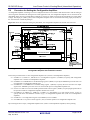
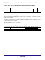
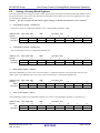
APPLICATION NOTE RL78/G1E Group Low-Power Control of Analog Block (Intermittent Operation) R01AN1128EJ0110 Rev.1.10 Sep. 30, 2013 Introduction This application note describes how to apply the low-power control for the sensor measurement by using the stanby function (HALT mode) of the microcontroller block and the power-off function of the analog block incorporated in the RL78/G1E (R5F10FMx). Operation Verified Devices RL78/G1E (R5F10FMx (x = C, D, or E)) When this application note is applied to other microcontrollers, make the necessary changes according to the specifications of the microcontroller and verify them thoroughly. R01AN1128EJ0110 Rev.1.10 Sep. 30, 2013 Page 1 of 38 RL78/G1E Group Low-Power Control of Analog Block (Intermittent Operation) Contents 1. Specifications ......................................................................................................................................... 3 2. Conditions for Verifying Operation ......................................................................................................... 4 3. Related Application Notes ...................................................................................................................... 4 4. Hardware ................................................................................................................................................ 5 4.1 Hardware Configuration Example............................................................................................... 5 4.2 Functions Used........................................................................................................................... 6 4.3 Pins Used ................................................................................................................................... 6 5. Features of the Analog Block ................................................................................................................. 7 5.1 Procedure for Setting the Variable Output Voltage Regulator.................................................... 7 5.2 Procedure for Setting the Configurable Amplifiers ..................................................................... 8 5.3 Procedure for Setting the D/A Converter.................................................................................... 9 5.4 Analog Block Settling Time....................................................................................................... 10 5.4.1 Settling time of the variable output voltage regulator........................................................ 10 5.4.2 Settling time of the configurable amplifier (used as transimpedance amplifier) ............... 10 5.4.3 D/A converter settling time................................................................................................ 11 6. Software ............................................................................................................................................... 12 6.1 Timing Chart ............................................................................................................................. 12 6.2 Settings of Analog Block Registers .......................................................................................... 14 6.3 Settings of Microcontroller Block Registers .............................................................................. 17 6.4 Functions .................................................................................................................................. 27 6.5 Function Specifications............................................................................................................. 28 6.6 RAM Variables.......................................................................................................................... 30 6.7 Flowcharts ................................................................................................................................ 31 6.8 Source Files and Changes Applied to the Code Output from the Code Generator ................. 36 R01AN1128EJ0110 Rev.1.10 Sep. 30, 2013 Page 2 of 38 RL78/G1E Group 1. Low-Power Control of Analog Block (Intermittent Operation) Specifications This application note describes the example of the low-power control introducing the intermittent operation to the sensor measurement with the RL78/G1E (R5F10FMx). In this application note, using the example of the system to measure the illuminance with the photodiode (BS520E0F made by Sharp Corporation) connected to the RL78/G1E (R5F10FMx), it is explained how to shift the microcontroller block and the analog block incorporated in the RL78/G1E (R5F10FMx) from the normal operation mode to the stanby mode, how to make a comeback to the normal operation mode, and how to use the CPU/peripheral function, the analog peripheral function after a comeback. Figure 1.1 shows an overview of the control flow used in this application note. Microcontroller block of RL78/G1E (R5F10FMx) Analog block of RL78/G1E (R5F10FMx) HALT state INTTM01 interrupt request Normal operation Operation stopped On control Wait for settling time Wait for 100 µs Operation starts Both the microcontroller block and the analog block are in the low-power state. The microcontroller block enters the normal operation state in response to an interrupt. The microcontroller block sends a SPI command to the analog block to start operating. Settling time AMP1_OUT output voltage Output stable The analog block output stabilizes after the settling time has elapsed. A/D conversion starts A/D conversion ends Off control Operation stops 10 ms cycle HALT state Once A/D conversion has finished, the microcontoller sends a SPI command to the analog block to stop operating. Both the microcontroller block and the analog block are in the low-power state. INTTM01 interrupt request Normal operation On control Operation starts The microcontroller block enters the normal operation state triggered by an interrupt The analog block starts operating based on communication from the microcontroller block via the SPI. Figure 1.1 Control Flow R01AN1128EJ0110 Rev.1.10 Sep. 30, 2013 Page 3 of 38 RL78/G1E Group 2. Low-Power Control of Analog Block (Intermittent Operation) Conditions for Verifying Operation The operation of the sample code shown in this application note has been verified under the conditions shown below. Table 2.1 Conditions for Verifying Operation Item Microcontroller used Operating frequency Operating voltage External devices used Integrated development environment C compiler 3. Description RL78/G1E (R5F10FME) High-speed on-chip oscillator (high-speed OCO) clock: 32 MHz CPU/peripheral hardware clock: 32 MHz VDD, DVDD, AVDD1, AVDD2, AVDD3: 5.0 V AVDD: 3.3 V LVD detection voltage (VLVIH): 4.06 V when rising, 3.98 V when falling Photodiode (BS520E0F made by Sharp Corporation) CubeSuite+ V1.01.01 [31 Jan 2012] made by Renesas Electronics CA78K0R V1.30 made by Renesas Electronics Related Application Notes Related application notes are shown below. Also refer to these documents when using this application note. RL78/G13 Low-Power Operation (R01AN0465E) Application Note RL78/G1E Example Measurement Using a Current Sensor (R01AN1055E) Application Note RL78/G1E Sample Code for Performing SPI Communication with Analog Block (R01AN1130E) Application Note R01AN1128EJ0110 Rev.1.10 Sep. 30, 2013 Page 4 of 38 RL78/G1E Group 4. Low-Power Control of Analog Block (Intermittent Operation) Hardware 4.1 Hardware Configuration Example Figure 4.1 shows an example of the hardware configuration described in this application note. 5.0 V MPXIN10 AVDD1 AVDD2 AVDD3 AGND1 Sensor (photodiode) AGND2 AGND3 Analog block AGND4 5.0 V AMP1_OUT DVDD DGND ARESET# DGND LDO_OUT DGND DGND BGR_OUT 5.0 V P70/SCLK# P71/SDO SPI communication P72/SDI P73/CS# 5.0 V AVDD VDD AVSS REGC VSS 2k Measured voltage subject to A/D conversion ANI2 Note 2 P130 Microcontroller block 3k Note 1: Because the A/D converter supply voltage is 3.3 V, the output of the AMP1_OUT pin (0 to 5 V) is stepped down to 0 to 3 V by using a resistor divider. Note 2: The analog block is reset via the P130 pin output. After the reset of the microcontroller block ends, P130 outputs a high level. 5.0 V Resistor divider Note 1 RESET# For on-chip debugging TOOL0 RL78/G1E (R5F10FMx) Figure 4.1 Hardware Configuration Caution This circuit diagram is simplified to show an overview of the circuit connections. When designing an actual circuit, connect pins appropriately so as to satisfy the electrical specifications. (Connect unused input-only ports individually to VDD or VSS via a resistor.) R01AN1128EJ0110 Rev.1.10 Sep. 30, 2013 Page 5 of 38 RL78/G1E Group 4.2 Low-Power Control of Analog Block (Intermittent Operation) Circuits Used Table 4.1 shows the RL78/G1E (R5F10FMx) peripheral circuits used in this application note and their applications. Table 4.1 RL78/G1E (R5F10FMx) Peripheral Circuits and Their Applications Microcontroller block Analog block RL78/G1E (R5F10FMx) Peripheral Circuit Configurable amplifier D/A converter Variable output voltage regulator SPI A/D converter High-speed on-chip oscillator (high-speed OCO) Serial array unit 1 (channel 1) I/O ports Timer array unit 0 (channel 1) Timer array unit 0 (channel 3) 4.3 Application Used as a transimpedance amplifier that converts the output current from a sensor (photodiode) to a single-ended voltage and amplifies it. Generates a bias voltage for the configurable amplifier (used as a transimpedance amplifier). Generates the power supply voltage for the A/D converter. Controls SPI communication with the microcontroller block of the RL78/G1E (R5F10FMx). Converts the voltage output from the configurable amplifier (used as a transimpedance amplifier) to a digital value. Generates the 32 MHz clock used as the main system clock. Controls SPI communication with the analog block by using the 3-wire serial I/O (CSI21). Controls the reset of the analog block, and the chip select signal (CS) used to control SPI communication with the analog block. The timer to generate the signal which cancels the HALT mode. The timer to generate the settling time that the system must wait until the output of configurable amplifier Ch1 (used as a transimpedance amplifier) and the D/A converter stabilizes. Pins Used Table 4.2 shows the RL78/G1E (R5F10FMx) pins used in this application note and their features. Table 4.2 RL78/G1E (R5F10FMx) Pins Used and Their Features Pin Name MPXIN10 AMP1_OUT I/O Input Output ANI2 Input P130 Output Description This is an inverted input pin of the configurable amplifier Ch1 (used as a transimpedance amplifier) in the analog block. This pin is connected to the sensor (Photodiode). This is an output pin of the configurable amplifier Ch1 (used as a transimpedance amplifier) in the analog block. This pin is connected to the ANI2 pin of the A/D converter in the microcontroller block via a resistor divider. This is an analog input pin of the A/D converter in the microcontroller block. This pin is connected to the AMP1_OUT pin in the analog block via a resistor divider. P130 is an output-only pin in the microcontroller block. This pin is connected to the ARESET# pin in the analog block and is used to control the analog reset feature of the analog block. R01AN1128EJ0110 Rev.1.10 Sep. 30, 2013 Page 6 of 38 RL78/G1E Group 5. Low-Power Control of Analog Block (Intermittent Operation) Features of the Analog Block See 6.2 Settings of Analog Block Registers on p. 14 for details. 5.1 Procedure for Setting the Variable Output Voltage Regulator The variable output voltage regulator incorporated in the RL78/G1E (R5F10FMx) is a series regulator which outputs the variable voltage from 2.0 to 3.3 V by a 0.1 V step with the setting of control registers. In this application note, the output voltage from the variable output voltage regulator is set to be 3.3 V and is used as the power supply voltage of the A/D converter. Figure 5.1 shows the connection between the variable output voltage regulator in the analog block and the A/D converter in the microcontroller block incorporated in the RL78/G1E (R5F10FMx). RL78/G1E (R5F10FMx) Analog block BGR_OUT 3.3 V (Typ.) LDO_OUT Reference voltage generator Variable output voltage regulator Microcontroller block AVDD Set the LDO_OUT pin output to 3.3 V (Typ.) and connect it to the AVDD pin of the A/D converter. A/D converter AVSS Figure 5.1 Connection Between Variable Output Voltage Regulator and A/D Converter Follow the procedure below to start the variable output voltage regulator (LDO_OUT = 3.3 V (Typ.)) and reference voltage generator in the analog block of the RL78/G1E (R5F10FMx)). <1> Set LDO3 to 1, LDO2 to 1, LDO1 to 0, and LDO0 to 1 in the LDO control register (LDOC) to specify 3.3 V (Typ.) as the voltage output from the variable output voltage regulator. <2> Set LDOOF to 1 in power control register 2 (PC2) to enable operation of the variable output voltage regulator and reference voltage generator. By executing the above steps, the variable output voltage regulator and reference voltage generator start operating and 3.3 V (Typ.) is output from the LDO_OUT pin. Follow the procedure below to stop the variable output voltage regulator and reference voltage generator. <1> Set LDOOF to 0 in power control register 2 (PC2) to stop operation of the variable output voltage regulator and reference voltage generator. By executing the above step, the variable output voltage regulator and reference voltage generator stop operating and 0 V is output from the LDO_OUT pin. In this application note, the output voltage from the variable output voltage regulator in the analog block is used as the power supply voltage of the A/D converter in the microcontroller block, so the variable output voltage regulator is never stopped once they start operating. R01AN1128EJ0110 Rev.1.10 Sep. 30, 2013 Page 7 of 38 RL78/G1E Group 5.2 Low-Power Control of Analog Block (Intermittent Operation) Procedure for Setting the Configurable Amplifiers A configurable amplifier can change its circuit configuration and its circuit features and characteristics with the setting of control registers included in the analog block. In this application note, the configurable amplifier Ch1 is connected to the photodiode and is used as a transimpedance amplifier to convert an output current from the photodiode to a single-ended voltage. The output pin (AMP1_OUT) of the configurable amplifier Ch1 is connected to the analog input pin (ANI2) of the A/D converter outside the packages. Selector Selector Figure 5.2 shows the connection among the photodiode, the configurable amplifier Ch1 and the A/D converter. Figure 5.2 Connection Between Configurable Amplifier Ch1 and Photodiode, and Between Configurable Amplifier Ch1 and A/D Converter Follow the procedure below to start configurable amplifier Ch1 (used as a transimpedance amplifier). <1> Set SW11 to 1, SW12 to 1, and SW13 to 1 in configuration register 1 (CONFIG1) to specify that configurable amplifier Ch1 is used as a transimpedance amplifier. <2> Set MPX11 to 0 and MPX10 to 0 in MPX setting register 1 (MPX1) to specify the MPXIN10 pin as the source of inverted input to configurable amplifier Ch1. <3> Set MPX21 to 1 and MPX20 to 0 in MPX setting register 1 (MPX1) to specify the D/A converter Ch1 output signal or the VREFIN1 pin as the source of non-inverted input to configurable amplifier Ch1. <4> Set CC1 to 0 and CC0 to 0 in the AMP operation mode control register (AOMC) to specify high-speed mode as the operation mode of configurable amplifier channels Ch1 to Ch3. <5> Set AMP14 to 0, AMP13 to 1, AMP12 to 1, AMP11 to 1, and AMP10 to 1 in gain control register 1 (GC1) to specify 640 kΩ as the feedback resistance (Typ.) of configurable amplifier Ch1 (used as a transimpedance amplifier). <6> Set SW01 to 1 in configuration register 2 (CONFIG2) to turn on SW01. <7> Set AMP1OF to 1 in power control register 1 (PC1) to enable operation of configurable amplifier Ch1. By executing the above steps, configurable amplifier Ch1 (used as a transimpedance amplifier) starts operating. R01AN1128EJ0110 Rev.1.10 Sep. 30, 2013 Page 8 of 38 RL78/G1E Group Low-Power Control of Analog Block (Intermittent Operation) Follow the procedure below to stop configurable amplifier Ch1 (used as a transimpedance amplifier). <1> Set AMP1OF to 0 in power control register 1 (PC1) to stop operation of configurable amplifier Ch1. By executing the above step, configurable amplifier Ch1 (used as a transimpedance amplifier) stops operating. In this application note, the operation of configurable amplifier Ch1 (used as a transimpedance amplifier) is stopped after its output voltage, which is a voltage that has been stepped down by using a resistor divider, has been A/D converted by the A/D converter in the microcontroller block. 5.3 Procedure for Setting the D/A Converter In this application note, D/A converter Ch1 in the analog block is used to generate a bias voltage for configurable amplifier Ch1 (used as a transimpedance amplifier). Follow the procedure below to start D/A converter Ch1. <1> Set VRT1 to 0 and VRT0 to 0 in the DAC reference voltage control register (DACRC) to specify “AVDD1 × 5/10” as the upper limit of the reference voltage (VRT) for the D/A converter. <2> Set VRB1 to 0 and VRB0 to 0 in the DAC reference voltage control register (DACRC) to specify AGND1 as the lower limit of the reference voltage (VRB) for the D/A converter. <3> Specify the analog voltage to be output to DAC control register 1 (DAC1C). • In this application note, D/A converter Ch1 is used to generate a bias voltage for configurable amplifier Ch1 (used as a transimpedance amplifier). Set the DAC1C register to 19H to specify 0.49 V as the voltage output from the DAC1_OUT pin. (Note that the value set to the DAC1C register is a reference value. The user needs to evaluate the system to determine the actual values.) • DAC1_OUT = ((reference voltage upper limit − reference voltage lower limit) × 2 × m/255) + 2 × reference voltage lower limit = ((AVDD1 × 5/10 − AGND1) × 2 × 25/255) + 2 × AGND1 = ((5 × 5/10 − 0) × 2 × 25/255) + 2 × 0 = 0.49 V * AVDD1 = 5 V * AGND1 = 0 V * m (DAC1C register value) = 25 (19H) <4> Set DAC1OF to 1 in power control register 1 (PC1) to enable operation of D/A converter Ch1. By executing the above steps, D/A converter Ch1 starts operating. Follow the procedure below to stop D/A converter Ch1. <1> Set DAC1OF to 0 in power control register 1 (PC1) to stop operation of D/A converter Ch1. By executing the above step, D/A converter Ch1 stops operating. In this application note, the operation of configurable amplifier Ch1 (used as a transimpedance amplifier) is stopped after its output voltage, which is a voltage that has been stepped down by using a resistor divider, has been A/D converted by the A/D converter in the microcontroller block. Due to this, the operation of D/A converter is also stopped. R01AN1128EJ0110 Rev.1.10 Sep. 30, 2013 Page 9 of 38 RL78/G1E Group 5.4 Low-Power Control of Analog Block (Intermittent Operation) Analog Block Settling Time 5.4.1 Settling time of the variable output voltage regulator When operation of the variable output voltage regulator is started (by setting LDOOF to 1 in power control register 2 (PC2)) after having been stopped (by setting LDOOF to 0 in PC2), a settling time (tSET) is required for the output of the variable output voltage regulator to stabilize. The required settling time of the variable output voltage regulator is shown in Table 5.1 below, based on the electrical specifications described in the RL78/G1E Hardware User’s Manual. Table 5.1 Settling Time of Variable Output Voltage Regulator (−40°C ≤ TA ≤ 85°C, AVDD1 = AVDD2 = AVDD3 = DVDD = 5.0 V, LDOOF = 1) Parameter Symbol Conditions Ratings MIN Settling time tSET − − Caution 5.4.2 Unit TYP − MAX 5 ms The rating in Table 5.1 applies to when a 4.7 μF (recommended value) capacitor is connected to the LDO_OUT pin and a 0.1 μF (recommended value) capacitor is connected to the BGR_OUT pin. Settling time of the configurable amplifier (used as transimpedance amplifier) When operation of the configurable amplifier is started (by setting AMPnOF (n = 1 to 3) to 1 in power control register 1 (PC1)) after having been stopped (by setting AMPnOF (n = 1 to 3) to 0 in PC1), a settling time (TS) is required for the output of the amplifier to stabilize. The settling time of the configurable amplifier (used as a non-inverting amplifier) is measured from the end of SPI command (the data that changes the setting of the AMPnOF (n = 1 to 3) bit from 0 to 1 is latched) until the output voltage from the configurable amplifier (AMPn_OUT (n = 1 to 3)) is within ±0.1% of the final output voltage.Figure 5.3 shows the settling time. CS# SCLK# TS AMPn_OUT (n = 1 to 3) Data that changes AMPnOF (n = 1 to 3) from 0 to 1 is latched Figure 5.3 Settling Time of Configurable Amplifier (Used as Transimpedance Amplifier) The required settling time of the configurable amplifier when used as a transimpedance amplifier is shown in Table 5.2 below, based on the electrical specifications described in the RL78/G1E Hardware User’s Manual. R01AN1128EJ0110 Rev.1.10 Sep. 30, 2013 Page 10 of 38 RL78/G1E Group Low-Power Control of Analog Block (Intermittent Operation) Table 5.2 Settling Time of Configurable Amplifier (Used as Transimpedance Amplifier) (−40°C ≤ TA ≤ 85°C, AVDD1 = AVDD2 = AVDD3 = DVDD = 5.0 V, AMP1OF = AMP2OF = AMP3OF = 1) Parameter Symbol Conditions Ratings MIN TYP MAX Settling time TS High-speed mode 9 − − (CC1, CC0 = 0, 0) Feedback resistance: 20 kΩ 5.4.3 Unit μs D/A converter settling time When operation of the D/A converter is started (by setting DACnOF (n = 1 to 4) to 1 in power control register 1 (PC1)) after having been stopped (by setting DACnOF (n = 1 to 4) to 0 in PC1), a settling time (tSET) is required for the output of the D/A converter to stabilize. The settling time of the D/A converter is measured from the end of SPI command (the data that changes the setting of the DACnOF (n = 1 to 4) bit from 0 to 1 is latched) until the output voltage from the D/A converter (DACn_OUT (n = 1 to 4)) is within ±1.0% of the final output voltage. The required settling time of the D/A converter is shown in Table 5.3 below, based on the electrical specifications described in the RL78/G1E Hardware User’s Manual. Table 5.3 D/A Converter Settling Time (−40°C ≤ TA ≤ 85°C, AVDD1 = AVDD2 = AVDD3 = DVDD = 5.0 V, DAC1OF = DAC2OF = DAC3OF = DAC4OF = 1) Parameter Symbol Conditions Unit Ratings MIN TYP MAX Settling time tSET 100 μs − − − R01AN1128EJ0110 Rev.1.10 Sep. 30, 2013 Page 11 of 38 RL78/G1E Group 6. 6.1 Low-Power Control of Analog Block (Intermittent Operation) Software Timing Chart In this application note, configurable amplifier Ch1 (used as a transimpedance amplifier) and D/A converter Ch1 are used. It is therefore necessary to program the system to wait for at least 100 us between when the AMP1OF and DAC1OF bits are set to 1 in the PC1 register and the start of A/D conversion, to accord with the D/A converter's settling time, which is the longer of the two. A timing chart showing the intermittent operation described in this application note is shown below. 10 ms TAU0 Ch1 INTTM01 CPU status HALT mode Normal operation mode TAU0 Ch3 HALT mode Normal operation mode 100 µs measured AMP1OF Operating (settling time) Status of configurable amplifier Ch1 Operation stopped Operating (output stable) Operation stopped DAC1OF Operating (output stable) Status of D/A converter Ch1 Operation stopped Operation stopped Operating (settling time) A/D converter ADCS <1> Remark INTTM01: AMP1OF: DAC1OF: ADCS: <2> <3> <4> <5> <6> <1> Interrupt triggered by the completion of counting by channel 1 of timer array unit 0 or capture interrupt Bit 0 of power control register 1 (PC1). Controls the operation of configurable amplifier Ch1. 0: Stop operation of configurable amplifier Ch1. 1: Enable operation of configurable amplifier Ch1. Bit 4 of power control register 1 (PC1). Controls the operation of D/A converter Ch1. 0: Stop operation of D/A converter Ch1. 1: Enable operation of D/A converter Ch1. Bit 7 of A/D converter mode register 0 (ADM0) 0: Stop conversion (When read: Conversion stopped or in the standby status) 1: Enable conversion (When read: Conversion in progress (software trigger mode)) Figure 6.1 Timing Chart for Intermittent Operation R01AN1128EJ0110 Rev.1.10 Sep. 30, 2013 Page 12 of 38 RL78/G1E Group Low-Power Control of Analog Block (Intermittent Operation) <1> The microcontroller block exits the HALT mode upon occurrence of the interrupt request triggered by the completion of counting by channel 1 of timer array unit 0 (INTTM01). <2> Operation of configurable amplifier Ch1 (used as a transimpedance amplifier) and D/A converter Ch1 in the analog block is started via the 3-wire serial I/O of channel 1 of serial array unit 1 (CSI21) in the microcontroller block (by setting the AMP1OF and DAC1OF bits to 1 in the PC1 register). <3> The system waits for 100 us, which is the settling time of configurable amplifier Ch1 (used as a transimpedance amplifier) and D/A converter Ch1 in the analog block, and which is counted by using the interval timer of channel 3 of timer array unit 0 in the microcontroller block. Once the 100 us wait time has elapsed, the A/D converter in the microcontroller block enters software trigger mode and A/D conversion of the data input from the ANI2 pin is started (by setting the ADCS bit to 1 in A/D converter mode register 0 (ADM0)). <4> When the A/D converter in the microcontroller block finishes A/D converting the data, the conversion result is read out. <5> Operation of configurable amplifier Ch1 (used as a transimpedance amplifier) and D/A converter Ch1 in the analog block is stopped via CSI21 in the microcontroller block (by setting the AMP1OF and DAC1OF bits to 0 in the PC1 register). <6> The microcontroller block enters HALT mode. R01AN1128EJ0110 Rev.1.10 Sep. 30, 2013 Page 13 of 38 RL78/G1E Group 6.2 Low-Power Control of Analog Block (Intermittent Operation) Settings of Analog Block Registers This section describes the settings of the SPI control registers in the analog block of the RL78/G1E (R5F10FMx) used in this application note. This section omits descriptions of the SPI control registers not used in this application note. (They are used with their default values.) Caution (1) For how to specify the SPI control register settings, see the RL78/G1E Hardware User’s Manual. Configuration register 1 (CONFIG1) Set all the switches of configurable amplifier Ch1 to "transimpedance amplifier" mode. Address: 00H Symbol CONFIG1 Set value (2) After reset: 00H 7 6 0 SW11 0 1 R/W 5 SW12 1 Set value: 70H 4 3 SW13 0 1 0 2 SW21 0 1 SW22 0 0 SW23 0 2 SW02 0 1 SW01 1 0 SW00 0 Configuration register 2 (CONFIG2) Turn on the output switches of configurable amplifier Ch1. Address: 01H Symbol CONFIG2 Set value (3) After reset: 00H 7 6 0 SW31 0 0 R/W 5 SW32 0 Set value: 02H 4 3 SW33 0 0 0 MPX setting register 1 (MPX1) Specify the MPXIN10 pin as the source of inverted input to configurable amplifier Ch1, and the D/A converter Ch1 output signal or the VREFIN1 pin as the source of non-inverted input to configurable amplifier Ch1. Address: 03H After reset: 00H Symbol 7 6 MPX1 MPX11 MPX10 0 0 Set value (4) R/W 5 MPX21 1 Set value: 20H 4 3 MPX20 MPX31 0 0 2 MPX30 0 1 MPX41 0 0 MPX40 0 Gain control register 1 (GC1) Set the feedback resistance of configurable amplifier Ch1 (used as a transimpedance amplifier) to 640 kΩ (Typ.). Address: 06H Symbol GC1 Set value After reset: 00H 7 6 0 0 0 0 R01AN1128EJ0110 Rev.1.10 Sep. 30, 2013 R/W 5 0 0 Set value: 0FH 4 3 AMPG14 AMPG13 0 1 2 AMPG12 1 1 AMPG11 1 0 AMPG10 1 Page 14 of 38 RL78/G1E Group (5) Low-Power Control of Analog Block (Intermittent Operation) AMP operation mode control register (AOMC) Set the operating mode of configurable amplifier Ch1 to “high-speed mode”. Address: 09H Symbol AOMC Set value (6) After reset: 00H 7 6 0 0 0 0 R/W 5 0 0 4 0 0 Set value: 00H 3 0 0 2 0 0 1 CC1 0 0 CC0 0 2 LDO2 1 1 LDO1 0 0 LDO0 1 LDO control register (LDOC) Set the output voltage of the variable output voltage regulator to 3.3 V (Typ.). Address: 0BH Symbol LDOC Set value (7) After reset: 0DH 7 6 0 0 0 0 R/W 5 0 0 Set value: 0DH 4 3 0 LDO3 0 1 DAC reference voltage control register (DACRC) Set the upper (VRT) and lower (VRB) limits of the reference voltage for the D/A converter to AVDD1 × 5/10 and AGND1, respectively. Address: 0CH After reset: 00H Symbol 7 6 DACRC 0 0 0 0 Set value (8) R/W 5 0 0 4 0 0 Set value: 00H 3 VRT1 0 2 VRT0 0 1 VRB1 0 0 VRB0 0 2 DAC12 0 1 DAC11 0 0 DAC10 1 DAC control register 1 (DAC1C) Set the analog voltage to be output to the DAC1_OUT pin to 0.49 V. Address: 0DH After reset: 80H Symbol 7 6 DAC1C DAC17 DAC16 0 0 Set value R01AN1128EJ0110 Rev.1.10 Sep. 30, 2013 R/W 5 DAC15 0 Set value: 19H 4 3 DAC14 DAC13 1 1 Page 15 of 38 RL78/G1E Group (9) Low-Power Control of Analog Block (Intermittent Operation) Power control register 1 (PC1) Enable or stop operation of configurable amplifier Ch1 and D/A converter Ch1. Address: 11H After reset: 00H Symbol 7 6 PC1 DAC4OF DAC3OF 0 0 Set value R/W 5 DAC2OF 0 Set value: **H 4 3 DAC1OF 0 * 0 2 AMP3OF 0 1 AMP2OF 0 0 AMP1OF * Remark: * = Write 1 to this bit to enable operation of configurable amplifier Ch1 and D/A converter Ch1, and 0 to stop operation. (10) Power control register 2 (PC2) Enable operation of the variable output voltage regulator and reference voltage generator. Address: 12H Symbol PC2 Set value After reset: 00H 7 6 0 0 0 0 R01AN1128EJ0110 Rev.1.10 Sep. 30, 2013 R/W 5 0 0 Set value: 02H 4 3 GAINOF LPFOF 0 0 2 HPFOF 0 1 LDOOF 1 0 TEMPOF 0 Page 16 of 38 RL78/G1E Group 6.3 Low-Power Control of Analog Block (Intermittent Operation) Settings of Microcontroller Block Registers The register settings specified for the microcontroller block of the RL78/G1E (R5F10FMx) are shown below. This section omits descriptions of the SPI control registers not used in this application note. (They are used with their default values.) Caution For how to specify the microcontroller block register settings, see the RL78/G1E Hardware User’s Manual. (1) User option bytes (a) User option byte (000C0H/010C0H) Disable operation of the watchdog timer counter. Address: 000C0H/010C0H Symbol 7 6 WDTINT WINDOW 1 1 1 Set value (b) 5 WINDOW 0 1 4 WDTON 3 WDCS2 0 1 Set value: EEH 2 1 WDCS1 WDCS0 1 1 0 WDSTBY ON 0 User option byte (000C1H/010C1H) Set the LVD operation mode to "reset mode", and the LVD detection level (VLVIH) when the voltage is rising to 4.06 V and when the voltage is falling to 3.98 V. Address: 000C1H/010C1H Symbol 7 6 VPOC2 VPOC1 0 1 Set value (c) 5 VPOC0 1 4 1 1 3 LVIS1 0 Set value: 73H 2 1 LVIS0 LVIMDS1 0 1 0 LVIMDS0 1 User option byte (000C2H/010C2H) Set the flash operation mode to "HS (high speed main) mode" and select 32 MHz as the high-speed on-chip oscillator frequency. Address: 000C2H/010C2H Symbol 7 6 CMODE1 CMODE0 5 1 4 0 1 1 0 Set value (d) 1 Set value: E8H 3 2 1 FRQSEL FRQSEL FRQSEL 3 2 1 1 0 0 0 FRQSEL 0 0 On-chip debug option byte (000C3H/010C3H) Enable on-chip debugging and specify that the flash memory data is erased if security ID authorization fails. Address: 000C3H/010C3H Symbol 7 OCDENS ET 1 Set value 6 0 5 0 4 0 3 0 0 0 0 0 R01AN1128EJ0110 Rev.1.10 Sep. 30, 2013 Set value: 84H 2 1 1 1 0 0 0 OCDERS D 0 Page 17 of 38 RL78/G1E Group Low-Power Control of Analog Block (Intermittent Operation) (2) Clock generator (a) Clock operation mode control register (CMC) Set the operation mode of the high-speed system clock pin to "input port". Address: FFFA0H Symbol 7 CMC EXCLK 0 Set value (b) After reset: 00H 6 5 OSCSEL 0 0 0 R/W 4 0 1 3 0 0 Set value: 10H 2 0 0 1 0 0 0 AMPH 0 Clock operation status control register (CSC) Set the operation mode of the high-speed system clock (in input port mode) to "input port" and the operation mode of the high-speed on-chip oscillator to "high-speed on-chip oscillator operating". Address: FFFA1H Symbol 7 CSC MSTOP 1 Set value (c) After reset: C0H 6 5 1 0 1 0 R/W 4 0 0 3 0 0 Set value: C0H 2 1 0 0 0 0 0 HIOSTOP 0 System clock control register (CKC) Select the high-speed on-chip oscillator clock (fMAIN) as the main system clock (fIH). Address: FFFA4H Symbol 7 CKC CLS 0 Set value (d) 6 0 0 After reset: 00H 5 MCS 0 R/W 4 MCM0 0 3 0 0 Set value: 00H 2 0 0 1 0 0 0 0 0 1 0 0 0 0 0 Operation speed mode control register (OSMC) Select the low-speed on-chip oscillator clock as the interval timer operation clock. Address: F00F3H Symbol 7 OSMC 0 Set value 0 After reset: 00H R/W 6 5 4 0 0 WUTMM CK0 0 0 1 R01AN1128EJ0110 Rev.1.10 Sep. 30, 2013 3 0 0 Set value: 10H 2 0 0 Page 18 of 38 RL78/G1E Group (e) Low-Power Control of Analog Block (Intermittent Operation) Peripheral enable register 0 (PER0) Enable the input clock supply to the A/D converter, serial array unit 1, and timer array unit 0. Address: F00F0H Symbol 7 PER0 RTCEN 0 Set value 6 0 0 After reset: 00H 5 ADCEN 1 (3) Serial array unit 1 (a) Serial mode register 11 (SMR11) R/W 4 0 0 3 SAU1EN 1 Set value: 29H 2 SAU0EN 0 1 0 0 0 TAU0EN 1 Specify the operation clock specified by the SPS1 register (CK10) as the operation clock for channel 1 (fMCK), the divided operation clock (fMCK) specified by the CKS11 bit as the transfer clock for channel 1 (fTCLK), CSI mode as the channel 1 operation mode, and the transfer end interrupt or buffer empty interrupt as the channel 1 interrupt source. 0 STS11 0 SIS110 1 0 0 MD112 MD111 MD110 0 0 1 0 2 0 6 Set value: 002*H 5 4 3 0 R/W 8 7 CCS11 Set value After reset: 0020H 12 11 10 9 CKS11 Address: F0152H, F0153H Symbol 15 14 13 SMR11 0 0 0 0 0 0 0 0 0 0 1 0 0 0 0 * Remark: * = Switch the transfer end interrupt (= 0) and buffer empty interrupt (= 1) by using software. (b) Serial communication operation setting register 11 (SCR11) Specify "transmission/reception" as the channel 1 operation mode, "Type 1" as the data and clock phase in CSI mode, "MSB first" as the data transfer order, and "8 bits" as the transfer data length. (c) PTC110 DIR11 0 0 SLC110 0 1 1 DLS110 0 PTC111 1 EOC11 2 0 Set value: C007H 5 4 3 CKP11 6 DAP11 R/W 8 7 RXE11 Set value After reset: 0087H 12 11 10 9 TXE11 Address: F015AH, F015BH Symbol 15 14 13 SCR11 1 1 0 0 0 0 0 0 0 0 0 0 0 1 1 1 Serial data register 11 (SDR11) Specify "fMCK/32" as the transfer clock generated by dividing the operation clock (fMCK). The lower 8 bits (bits 7 to 0) function as a transmission/reception buffer register. Address: FFF4AH, FFF4BH Symbol 15 14 13 SDR11 − − − 0 0 0 Set value After reset: 0000H 12 11 10 9 − − − − 1 1 1 1 R/W 8 7 − − 0 * 6 − * Set value: 1E**H 5 4 3 − − − * * * 2 − * 1 − * 0 − * Remark: * = Functions as a transmission/reception buffer register. R01AN1128EJ0110 Rev.1.10 Sep. 30, 2013 Page 19 of 38 RL78/G1E Group (d) Low-Power Control of Analog Block (Intermittent Operation) Serial channel stop register 1 (ST1) Specify whether the trigger to stop operation of channel 1 is the "no trigger operation" or "clear the SE11 bit to 0 to stop the communication operation". 0 0 0 0 0 0 0 ST11 ST10 0 0 1 0 2 0 Set value: 000*H 5 4 3 0 6 0 R/W 8 7 0 Set value After reset: 0000H 12 11 10 9 0 Address: F0164H, F0165H Symbol 15 14 13 ST1 0 0 0 0 0 0 0 0 0 0 0 0 0 0 * 0 Remark: * = Write 1 to this bit only when finishing serial communication. (e) Serial clock select register 1 (SPS1) Specify "32 MHz when fCLK = 32 MHz" as the operation clock (CK10). (f) 0 PRS113 PRS112 PRS111 PRS110 PRS103 PRS102 PRS101 PRS100 0 0 1 0 2 0 Set value: 0000H 5 4 3 0 6 0 R/W 8 7 0 Set value After reset: 0000H 12 11 10 9 0 Address: F0166H, F0167H Symbol 15 14 13 SPS1 0 0 0 0 0 0 0 0 0 0 0 0 0 0 0 0 Serial output register 1 (SO1) Set the serial clock output of channel 1 to "1" and the serial data output to "0". (g) CKO10 0 0 0 0 0 0 SO11 SO10 0 CKO11 1 0 2 0 Set value: 0301H 5 4 3 0 6 0 R/W 8 7 0 Set value After reset: 0F0FH 12 11 10 9 0 Address: F0168H, F0169H Symbol 15 14 13 SO1 0 0 0 0 0 0 1 1 0 0 0 0 0 0 0 1 Serial output enable register 1 (SOE1) Specify whether to enable the serial output of channel 1 during serial communication. 0 0 0 0 0 0 0 SOE11 SOE10 0 0 1 0 2 0 Set value: 000*H 5 4 3 0 6 0 R/W 8 7 0 Set value After reset: 0000H 12 11 10 9 0 Address: F016AH, F016BH Symbol 15 14 13 SOE1 0 0 0 0 0 0 0 0 0 0 0 0 0 0 * 0 Remark: * = Write 1 to this bit to start serial communication and 0 to stop serial communication. R01AN1128EJ0110 Rev.1.10 Sep. 30, 2013 Page 20 of 38 RL78/G1E Group (h) Low-Power Control of Analog Block (Intermittent Operation) Serial channel start register 1 (SS1) Specify that the trigger to start operation of channel 1 is "clear the SE11 bit to 1 and enter the communication wait status". 0 0 0 0 0 0 0 SS11 SS10 0 0 1 0 2 0 Set value: 000*H 5 4 3 0 6 0 R/W 8 7 0 Set value After reset: 0000H 12 11 10 9 0 Address: F0162H, F0163H Symbol 15 14 13 SS1 0 0 0 0 0 0 0 0 0 0 0 0 0 0 * 0 Remark: * = Write 1 to this bit only when starting serial communication. (4) Ports (a) Port mode registers Select the Pmn pin I/O mode (m = 0 to 2, 4, 6, 7, 14, 15; n = 0 to 7). Address: FFF20H Symbol 7 PM0 1 1 Set value After reset: FFH 6 5 PM06 PM05 0 0 R/W Address: FFF21H Symbol 7 PM1 1 1 Set value After reset: FFH 6 5 PM16 PM15 0 1 R/W Address: FFF22H Symbol 7 PM2 PM27 0 Set value After reset: FFH 6 5 PM26 PM25 0 0 R/W Address: FFF24H Symbol 7 PM4 1 1 Set value After reset: FFH 6 5 1 1 1 1 R/W Address: FFF26H Symbol 7 PM6 1 1 Set value After reset: FFH 6 5 1 1 1 1 R/W Address: FFF27H Symbol 7 PM7 PM77 0 Set value After reset: FFH 6 5 PM76 PM75 0 0 R/W Address: FFF2EH Symbol 7 PM14 1 1 Set value After reset: FFH 6 5 1 1 1 1 R/W R01AN1128EJ0110 Rev.1.10 Sep. 30, 2013 Set value: 9FH 3 2 PM03 PM02 1 1 1 PM01 1 0 PM00 1 Set value: BFH 3 2 PM13 PM12 1 1 1 PM11 1 0 PM10 1 Set value: 1FH 3 2 PM23 PM22 1 1 1 PM21 1 0 PM20 1 4 1 1 Set value: F7H 3 2 PM43 PM42 0 1 1 PM41 1 0 PM40 1 4 1 1 Set value: F0H 3 2 PM63 PM62 0 0 1 PM61 0 0 PM60 0 4 PM74 0 Set value: 02H 3 2 PM73 PM72 0 0 1 PM71 1 0 PM70 0 Set value: FDH 3 2 1 1 1 1 1 PM141 0 0 PM140 1 4 PM04 1 4 PM14 1 4 PM24 1 4 1 1 Page 21 of 38 RL78/G1E Group Address: FFF2FH Symbol 7 PM15 1 1 Set value (b) Low-Power Control of Analog Block (Intermittent Operation) After reset: FFH 6 5 1 1 1 1 R/W 4 PM154 0 Set value: E0H 3 2 PM153 PM152 0 0 1 PM151 0 0 PM150 0 Set value: 00H 3 2 P03 P02 0 0 1 P01 0 0 P00 0 Set value: 00H 3 2 P13 P12 0 0 1 P11 0 0 P10 0 Set value: 00H 3 2 P23 P22 0 0 1 P21 0 0 P20 0 4 0 0 Set value: 00H 3 2 0 P42 0 0 1 P41 0 0 P40 0 4 0 0 Set value: 0*H 3 2 P73 P72 * 1 1 P71 0 0 P70 1 4 0 0 Set value: 01H 3 2 0 0 0 0 1 0 0 0 P130 1 4 0 0 Set value: 00H 3 2 0 0 0 0 1 0 0 0 P140 0 Port registers Control the Pmn pin output data (m = 0 to 2, 4, 7, 13, 14; n = 0 to 5 and 7). Address: FFF00H Symbol 7 P0 0 0 Set value After reset: 00H 6 5 0 0 0 0 R/W Address: FFF01H Symbol 7 P1 0 0 Set value After reset: 00H 6 5 0 P15 0 0 R/W Address: FFF02H Symbol 7 P2 0 0 Set value After reset: 00H 6 5 0 0 0 0 R/W Address: FFF04H Symbol 7 P4 0 0 Set value After reset: 00H 6 5 0 0 0 0 R/W Address: FFF07H Symbol 7 P7 0 0 Set value After reset: 00H 6 5 0 0 0 0 R/W Address: FFF0DH Symbol 7 P13 P137 0 Set value After reset: Undefined 6 5 0 0 0 0 R/W Address: FFF0EH Symbol 7 P14 0 0 Set value After reset: 00H 6 5 0 0 0 0 R/W 4 P04 0 4 P14 0 4 P24 0 Remark: * = Write 0 or 1 to switch the output level according to the status. R01AN1128EJ0110 Rev.1.10 Sep. 30, 2013 Page 22 of 38 RL78/G1E Group (c) Low-Power Control of Analog Block (Intermittent Operation) Port mode control register 7 (PMC7) Specify whether the P70 pin is used as a digital I/O pin or an analog input pin. Address: FFF67H Symbol 7 PMC7 1 1 Set value After reset: FFH 6 5 1 1 1 1 (5) A/D converter (a) A/D converter mode register 0 (ADM0) R/W 4 1 1 Set value: FEH 3 2 1 1 1 1 1 1 1 0 PMC70 0 Enable A/D conversion, specify "select" as the A/D conversion channel selection mode, enable operation of the A/D voltage comparator, and set the A/D conversion time to 54 μs (12-bit A/D conversion, no stabilization wait (hardware trigger no-wait mode), AVDD = 2.7 to 3.6 V, fCLK = 32 MHz). Address: FFF30H Symbol 7 ADM0 ADCS * Set value After reset: 00H 6 5 ADMD FR2 0 0 R/W 4 FR1 0 Set value: *1H 3 2 FR0 LV1 0 0 1 LV0 0 0 ADCE 1 Remark: * = Write 1 to this bit only when starting A/D conversion. (b) A/D converter mode register 1 (ADM1) Specify software trigger mode as the A/D conversion trigger mode and one-shot conversion mode as the A/D conversion operation mode. Address: FFF32H After reset: 00H R/W Symbol 7 6 5 4 ADM1 ADTMD1 ADTMD0 ADSCM 0 0 0 1 0 Set value (c) Set value: 20H 3 2 0 0 0 0 1 ADTRS1 0 0 ADTRS0 0 A/D converter mode register 2 (ADM2) Specify AVDD as the positive reference voltage supply of the A/D converter, AVSS as the negative reference voltage supply of the A/D converter, the generation of an interrupt signal (INTAD) if the conversion result upper/lower limit check results in ADLL register value ≤ ADCR register value ≤ ADUL register value, disable the SNOOZE mode, and set the A/D conversion resolution to "12 bits". Address: F0010H After reset: 00H R/W Symbol 7 6 5 4 ADM2 ADREFP1 ADREFP0 ADREFM 0 0 0 0 0 Set value R01AN1128EJ0110 Rev.1.10 Sep. 30, 2013 Set value: 00H 3 2 ADRCK AWC 0 0 1 0 0 0 ADTYP 0 Page 23 of 38 RL78/G1E Group (d) Low-Power Control of Analog Block (Intermittent Operation) Conversion result comparison upper limit setting register (ADUL) Set the A/D conversion result comparison upper limit to FFH. Address: F0011H Symbol 7 ADUL ADUL7 1 Set value (e) After reset: FFH 6 5 ADUL6 ADUL5 1 1 R/W 4 ADUL4 1 Set value: FFH 3 2 ADUL3 ADUL2 1 1 1 ADUL1 1 0 ADUL0 1 1 ADLL1 0 0 ADLL0 0 1 ADS1 1 0 ADS0 0 Conversion result comparison lower limit setting register (ADLL) Set the A/D conversion result comparison lower limit to 00H. Address: F0012H Symbol 7 ADLL ADLL7 0 Set value (f) After reset: 00H 6 5 ADLL6 ADLL5 0 0 R/W 4 ADLL4 0 Set value: 00H 3 2 ADLL3 ADLL2 0 0 Analog input channel specification register (ADS) Specify ANI2 as the A/D conversion channel (in select mode (ADMD = 0)). Address: FFF31H Symbol 7 ADS ADISS 0 Set value (g) After reset: 00H 6 5 0 0 0 0 R/W 4 ADS4 0 Set value: 02H 3 2 ADS3 ADS2 0 0 A/D port configuration register (ADPC) Specify "analog input" (not "digital I/O") as the I/O mode of the P24/ANI4, P23/ANI3, P22/ANI2, P21/ANI1, and P20/ANI0 pins. Address: F0076H Symbol 7 ADPC 0 0 Set value After reset: 00H 6 5 0 0 0 0 R01AN1128EJ0110 Rev.1.10 Sep. 30, 2013 R/W 4 0 0 Set value: 00H 3 2 0 ADPC2 0 0 1 ADPC1 0 0 ADPC0 0 Page 24 of 38 RL78/G1E Group Low-Power Control of Analog Block (Intermittent Operation) (6) Timer array unit 0 (a) Timer channel stop register 0 (TT0) Specify “no trigger operation” as the trigger to stop operation of channel 3 and “operation is stopped (stop trigger is generated)” as that of channel 1. 0 TT07 TT06 TT05 TT04 TT03 TT02 TT01 TT00 0 TTH01 1 0 2 TTH03 Set value: 000*H 5 4 3 0 6 0 R/W 8 7 0 Set value After reset: 0000H 12 11 10 9 0 Address: F01B4H, F01B5H Symbol 15 14 13 TT0 0 0 0 0 0 0 0 0 0 0 0 0 * 0 * 0 Remark: * = Write 1 to this bit during timer operation to stop the timer operation. (b) Timer clock selection register 0 (TPS0) Specify "32 MHz (fCLK = 32 MHz)" as the CK00 operation clock and "4 MHz (fCLK = 32 MHz)" as the CK01 operation clock. (c) PRS021 PRS020 PRS013 PRS012 PRS011 PRS010 PRS003 PRS002 PRS001 PRS000 0 0 1 0 2 PRS030 6 Set value: 0030H 5 4 3 PRS031 R/W 8 7 0 Set value After reset: 0000H 12 11 10 9 0 Address: F01B6H, F01B7H Symbol 15 14 13 TPS0 0 0 0 0 0 0 0 0 0 0 1 1 0 0 0 0 Timer mode registers 1 and 3 (TMR01, TMR03) Set timer mode registers 1 and 3 as follows: • Set the operation clock of channel 1 (fMCK) to "operation clock CK01 set by TPS0". • Set the operation clock of channel 3 (fMCK) to "operation clock CK00 set by TPS0" • Set the count clock of channels 3 and 1 (fTCLK) to "operation clock (fMCK) specified by the CKS0n0 and CKS0n1 (n = 1 to 3) bits". • Specify that channels 3 and 1 are used as 8-bit timers (not 16-bit timers). • Specify "only software trigger start is valid (other trigger sources are unselected)" as the start trigger and capture trigger for channels 3 and 1. • Specify the interval timer as the operation mode of channels 3 and 1. • Specify "timer interrupt is not generated when counting is started (timer output does not change, either)" as the count start and interrupt setting for channels 3 and 1. STS010 CIS011 CIS010 0 0 MD013 MD012 MD011 MD010 0 STS011 1 STS012 2 SPLIT01 Set value: 8000H 5 4 3 CCS01 6 0 R/W 8 7 CKS010 Set value After reset: 0000H 12 11 10 9 CKS011 Address: F0192H, F0193H Symbol 15 14 13 TMR01 1 0 0 0 0 0 0 0 0 0 0 0 0 0 0 0 R01AN1128EJ0110 Rev.1.10 Sep. 30, 2013 Page 25 of 38 RL78/G1E Group Low-Power Control of Analog Block (Intermittent Operation) (d) STS031 STS030 CIS031 CIS030 0 0 MD033 MD032 MD031 MD030 0 STS032 1 SPLIT03 2 CCS03 6 Set value: 0000H 5 4 3 0 R/W 8 7 CKS030 Set value After reset: 0000H 12 11 10 9 CKS031 Address: F0196H, F0197H Symbol 15 14 13 TMR03 0 0 0 0 0 0 0 0 0 0 0 0 0 0 0 0 Timer data registers 1 and 3 (TDR01, TDR03) Specify the interval in the interval mode of channels 1 and 3 of timer array unit 0. Address: FFF1AH, FFF1BH Symbol 15 14 13 TDR01 − − − 1 0 0 Set value After reset: 0000H 12 11 10 9 − − − − 1 1 1 0 R/W 8 7 − − 0 0 6 − 0 Set value: 9C3FH 5 4 3 − − − 1 1 1 2 − 1 1 − 1 0 − 1 Address: FFF66H, FFF67H Symbol 15 14 13 TDR03 − − − 0 0 0 Set value After reset: 0000H 12 11 10 9 − − − − 0 0 0 0 R/W 8 7 − − 0 0 6 − 0 Set value: 001FH 5 4 3 − − − 0 1 1 2 − 1 1 − 1 0 − 1 (e) Timer channel start register 0 (TS0) Specify that the trigger to start operation of channel 1 and channel 3 is the setting of the TE01 and TE03 bits to 1, enabling counting. TSH01 0 TS07 TS06 TS05 TS04 TS03 TS02 TS01 TS00 0 0 1 TSH03 2 0 6 Set value: 000*H 5 4 3 0 R/W 8 7 0 Set value After reset: 0000H 12 11 10 9 0 Address: F01B2H, F01B3H Symbol 15 14 13 TS0 0 0 0 0 0 0 0 0 0 0 0 0 * 0 * 0 Remark: * = Write 1 to this bit only when starting the timer. R01AN1128EJ0110 Rev.1.10 Sep. 30, 2013 Page 26 of 38 RL78/G1E Group 6.4 Low-Power Control of Analog Block (Intermittent Operation) Functions Table 6.1 Functions File Name main.c r_systeminit.c r_cg_cgc.c r_cg_port.c r_cg_serial.c r_cg_serial_user.c r_cg_adc.c r_cg_adc_user.c r_cg_timer.c r_cg_timer_user.c Function Name main R5F10FMx_LDO_Enable R5F10FMx_Analog_Init R5F10FMx_Analog_Start R5F10FMx_Analog_Stop R_Systeminit hdwinit R_CGC_Create R_PORT_Create R_SAU1_Create R_CSI21_Create R_CSI21_Start R_CSI21_Stop R_CSI21_Send_Receive r_csi21_interrupt r_csi21_callback_receiveend r_csi21_callback_error SPI_ControlRegister_Read SPI_ControlRegister_Write SPI_ControlRegister_Write_ Verify SPI_ControlRegister_Read_ Bit SPI_ControlRegister_Write_ Bit SPI_ControlRegister_Write_ Verify_Bit R_ADC_Create R_ADC_Start R_ADC_Stop R_ADC_Set_OperationOn R_ADC_Set_OperationOff R_ADC_Get_Result ADC_Control R_TAU0_Create R_TAU0_Channel1_Start R_TAU0_Channel1_Stop R_TAU0_Channel3_Start R_TAU0_Channel3_Stop r_tau0_channel1_interrupt TAU0_WAIT_1us R01AN1128EJ0110 Rev.1.10 Sep. 30, 2013 Overview main function Analog block LDO initialization function Analog block initialization function Analog block operation start function Analog block operation stop function MCU initialization function System initialization function Clock generator initialization function Port initialization function SAU1 initialization function CSI21 initialization function CSI21 operation start function CSI21 operation stop function CSI21 transmission/reception function INTCSI21 interrupt service function CSI21 reception completion function CSI21 error handling function SPI control register read function SPI control register write function SPI control register write verify function SPI control register bit read function SPI control register bit write function SPI control register bit write verify function ADC initialization function ADC operation start function ADC operation stop function ADC comparator operation enable function ADC comparator operation stop function A/D conversion result read function A/D conversion control function TAU0 initialization function TAU0 Ch1 counter operation start function TAU0 Ch1 counter operation stop function TAU0 Ch3 counter operation start function TAU0 Ch3 counter operation stop function TAU0 Ch1 interrupt service function 1-μs unit wait function Page 27 of 38 RL78/G1E Group 6.5 Low-Power Control of Analog Block (Intermittent Operation) Function Specifications The specifications of the major functions used in this application note are described below. For details about using the SPI to communicate with the analog block, see Sample Code for Performing SPI Communication with Analog Block (R01AN1130E). (1) main function Declaration Overview Parameters Return value Description (2) Analog block LDO initialization function (R5F10FMx_LDO_Enable) Declaration Overview Parameters Return value Description (3) void main(void) Main routine function None None • Initializes the variable output voltage regulator in the analog block. • Initializes timer array unit 0 in the microcontroller block. • Executes processing to make the system wait for the output of the variable output voltage regulator in the analog block to stabilize. • Initializes the A/D converter in the microcontroller block. • Initializes the circuits (configurable amplifier Ch1 and D/A converter Ch1) in the analog block. • Starts counting using channel 1 in timer array unit 0 in the microcontroller block. • Starts operation of the circuits (configurable amplifier Ch1 and D/A converter Ch1) in the analog block. • Waits for the 100 μs settling time. • Controls A/D conversion performed by the A/D converter in the microcontroller block. • Stops operation of the circuits (configurable amplifier Ch1 and D/A converter Ch1) in the analog block. • Shifts the microcontroller block to HALT mode. static uinu8_t R5F10FMx_LDO_Enable(void) Analog block LDO initialization function None 0: Successful 1: Communication with the analog block failed • Initializes the variable output voltage regulator in the analog block. - Sets the variable output voltage regulator voltage to 3.3 V and enables the variable output voltage regulator and the reference voltage generator. Analog block initialization function (R5F10FMx_Analog_Init) Declaration Overview Parameters Return value Description static uinu8_t R5F10FMx_Analog_Init(void) Analog block initialization function None 0: Successful 1: Communication with the analog block failed • Initializes the circuits in the analog block. - Configures configurable amplifier CH1 (used as a transimpedance amplifier) as shown in this application note. - Sets the D/A converter Ch1 output voltage. - Enables D/A converter Ch1 and configurable amplifier Ch1. R01AN1128EJ0110 Rev.1.10 Sep. 30, 2013 Page 28 of 38 RL78/G1E Group (4) Analog block operation start function (R5F10FMx_Analog_Start) Declaration Overview Parameters Return value Description (5) Description void R_Systeminit(void) MCU initialization function None None • Initializes the peripheral hardware in the MCU used in this application note. - Calls the R_PORT_Create function to initialize the ports. - Calls the R_CGC_Create function to initialize the clock generator. - Calls the R_SAU1_Create function to initialize the 3-wire serial I/O (CSI21) of channel 1 in serial array unit 1. System initialization function (hdwinit) Declaration Overview Parameters Return value Description (8) static uinu8_t R5F10FMx_Analog_Stop(void) Analog block operation stop function None 0: Successful 1: Communication with the analog block failed • Stops operation of the circuits in the analog block. - Stops operation of D/A converter Ch1 and configurable amplifier Ch1. MCU initialization function (R_Systeminit) Declaration Overview Parameters Return value Description (7) static uinu8_t R5F10FMx_Analog_Start(void) Analog block operation start function None 0: Successful 1: Communication with the analog block failed • Starts operation of the circuits in the analog block. - Enables D/A converter Ch1 and configurable amplifier Ch1. Analog block operation stop function (R5F10FMx_Analog_Stop) Declaration Overview Parameters Return value (6) Low-Power Control of Analog Block (Intermittent Operation) void hdwinit(void) System initialization function None None • Disables interrupts. • Calls the R_Systeminit function to initialize the MCU. • Enables interrupts. A/D conversion control function (ADC_Control) Declaration Overview Parameters Return value Description void ADC_Control(void) A/D conversion control function None None Controls A/D conversion of the voltage output from the configurable amplifier (Ch1) (voltage stepped down by using a resistor divider). R01AN1128EJ0110 Rev.1.10 Sep. 30, 2013 Page 29 of 38 RL78/G1E Group (9) 1-μs unit wait function (TAU0_WAIT_1us) Declaration Overview Parameters Return value Description 6.6 Low-Power Control of Analog Block (Intermittent Operation) void TAU0_WAIT_1us(uint32_t wait_1us) 1-μs unit wait function uint32_t wait_1us: 1-μs counter None • Calls the R_TAU0_Channel3_Stop function to stop counting using channel 3 in timer array unit 0. • Calls the R_TAU0_Channel3_Start function to start counting using channel 3 in timer array unit 0. • Decrements the value of the wait_1us parameter for the interval of channel 3 in timer array unit 0 (1 μs) until the value becomes 0. RAM Variables Table 6.2 RAM Variables Data Type Variable Name Description volatile uint8_t * volatile uint16_t volatile uint16_t gp_csi21_rx_address Address of CSI21 reception buffer Number of bytes received at CSI21 CSI21 received byte counter volatile uint8_t * volatile uint16_t gp_csi21_tx_address volatile uint16_t static uint16_t static uint8_t g_csi21_tx_count g_csi21_rx_length g_csi21_rx_count g_csi21_send_length _ad_buffer g_csi21_overrun_flag R01AN1128EJ0110 Rev.1.10 Sep. 30, 2013 Address of CSI21 transmission buffer Number of bytes transmitted from CSI21 CSI21 transmitted byte counter Stores the A/D conversion result. CSI21 overrun flag Function That Uses This Variable R_CSI21_Send_Receive r_csi21_interrupt None None R_CSI21_Send_Receive r_csi21_interrupt R_CSI21_Send_Receive r_csi21_interrupt R_CSI21_Send_Receive r_csi21_interrupt r_adc_interrupt ADC_Get_AD_Buffer_Value R_CSI21_Send_Receive r_csi21_callback_error SPI_ControlRegister_Read SPI_ControlRegister_Write Page 30 of 38 RL78/G1E Group 6.7 Low-Power Control of Analog Block (Intermittent Operation) Flowcharts Figure 6.2 shows an overview of the processing flow used in this application note. Flowcharts for the major functions are shown in the subsequent figures. Start … System initialization function The relevant option byte is referenced before the initial setup function is called. hdwinit() main() … main function End Figure 6.2 Overview of Processing Flow (1) System initialization function (hdwinit) hdwinit DI() R_Systeminit() EI() … Disables interrupts. … MCU initialization function Initializes the MCU described in this application note. … Enables interrupts. return Figure 6.3 Flowchart for hdwinit Function R01AN1128EJ0110 Rev.1.10 Sep. 30, 2013 Page 31 of 38 RL78/G1E Group (2) Low-Power Control of Analog Block (Intermittent Operation) MCU initialization function (R_Systeminit) R_Systeminit PIOR = 0x00U R_PORT_Create() R_CGC_Create() … Initializes peripheral I/O redirect. … Port initialization function Initializes the ports described in this application note. … Clock generator initialization function Initializes the clock generator described in this application note. R_SAU1_Create() … SAU1 initialization function Initializes the 3-wire serial I/O (CSI21) of channel 1 of serial array unit 1 described in this application note. CRC0CTL = 0x00U … Initializes the flash memory CRC calculation unit. IAWCTL = 0x00U … Initializes the illegal memory access detection, RAM guard, and SFR guard features. return Figure 6.4 Flowchart for R_Systeminit Function R01AN1128EJ0110 Rev.1.10 Sep. 30, 2013 Page 32 of 38 RL78/G1E Group (3) Low-Power Control of Analog Block (Intermittent Operation) main function (main) main R5F10FMx_LDO _Enable() Has communication with the analog block finished successfully? No ... Analog block LDO initialization function Initializes the variable output voltage regulator incorporated in the RL78/G1E (R5F10FMx). Yes ... Disables interrupts. DI() ... TAU0 initialization function Initializes timer array unit 0 in the RL78/G1E (R5F10FMx). R_TAU0_Create() ... 1-µs unit wait function Executes processing to make the system wait (5 ms) for the output of the variable output voltage regulator in the analog block to stabilize. TAU0_WAIT_1us(5000) ... ADC initialization function Initializes the A/D converter incorporated in the RL78/G1E (R5F10FMx). R_ADC_Create() ... Enables interrupts. EI() R5F10FMx_Analog _Init() Has communication with the analog block finished successfully? No ... Analog block initialization function Initializes configurable amplifier Ch1 and D/A converter Ch1 incorporated in the RL78/G1E (R5F10FMx). Yes R_TAU0_Channel1 _Start() ... TAU0 Ch1 counter operation start function Starts operation of the TAU0 Ch1 counter. R5F10FMx_Analog _Start() Has communication with the analog block finished successfully? No ... Analog block operation start function Starts operation of configurable amplifier Ch1 and D/A converter Ch1 in the RL78/G1E (R5F10FMx). Yes ... 1-µs unit wait function Makes the system wait for the settling time of configurable amplifier Ch1 and D/A converter Ch1 (at least 100 µs). TAU0_WAIT_1us(100) ... A/D conversion control function Controls A/D conversion of the voltage (voltage stepped down by using a resistor divider) output from configurable amplifier Ch1 (used as a transimpedance amplifier). ADC_Control() R5F10FMx_Analog _Stop() Has communication with the analog block finished successfully? No ... Analog block operation stop function Stops operation of configurable amplifier Ch1 and D/A converter Ch1 in the RL78/G1E (R5F10FMx). Yes HALT() ... The CPU enters HALT mode. Figure 6.5 Flowchart for main Function R01AN1128EJ0110 Rev.1.10 Sep. 30, 2013 Page 33 of 38 RL78/G1E Group (4) Low-Power Control of Analog Block (Intermittent Operation) Analog block LDO initialization function (R5F10FMx_LDO_Enable) R5F10FMx_LDO_Enable SPI_ControlRegis ter_Write() Has communication with the analog block finished successfully? ... SPI control register write function Writes data to the SPI control register in the RL78/G1E (R5F10FMx). - LDOC (0BH) = 0DH - PC2 (12H) = 02H No ... Returns 0 if writing the SPI control register was completed successfully, and 1 if an error occurred Yes return (0) return (1) Figure 6.6 Flowchart for R5F10FMx_LDO_Enable Function (5) Analog block initialization function (R5F10FMx_Analog_Init) R5F10FMx_Analog_Init SPI_ControlRegister _Write() Has communication with the analog block finished successfully? ... SPI control register write function Writes data to the SPI control register in the RL78/G1E (R5F10FMx). - CONFIG1 (00H) = 70H - CONFIG2 (01H) = 02H - MPX1 (03H) = 20H - GC1 (06H) = 0FH - AOMC (09H) = 00H - DACRC (0CH) = 00H - DAC1C (0DH) = 19H No ... Returns 0 if writing the SPI control register was completed successfully, and 1 if an error occurred Yes return (0) return (1) Figure 6.7 Flowchart for R5F10FMx_Analog_Init Function R01AN1128EJ0110 Rev.1.10 Sep. 30, 2013 Page 34 of 38 RL78/G1E Group (6) Low-Power Control of Analog Block (Intermittent Operation) Analog block operation start function (R5F10FMx_Analog_Start) R5F10FMx_Analog_Start SPI_ControlRegis ter_Write() Has communication with the analog block finished successfully? ... SPI control register write function Writes data to the SPI control register in the RL78/G1E (R5F10FMx). - PC1 (11H) = 11H No ... Returns 0 if writing the SPI control register was completed successfully, and 1 if an error occurred Yes return (1) return (0) Figure 6.8 Flowchart for R5F10FMx_Analog_Start Function (7) Analog block operation stop function (R5F10FMx_Analog_Stop) R5F10FMx_Analog_Stop SPI_ControlRegis ter_Write() Has communication with the analog block finished successfully? ... SPI control register write function Writes data to the SPI control register in the RL78/G1E (R5F10FMx). - PC1 (11H) = 00H No ... Returns 0 if writing the SPI control register was completed successfully, and 1 if an error occurred Yes return (0) return (1) Figure 6.9 Flowchart for R5F10FMx_Analog_Stop Function R01AN1128EJ0110 Rev.1.10 Sep. 30, 2013 Page 35 of 38 RL78/G1E Group 6.8 Low-Power Control of Analog Block (Intermittent Operation) Source Files and Changes Applied to the Code Output from the Code Generator The sample code used in this application note was created based on the code for the RL78/G1A group (R5F10ELE) output by the code generator of CubeSuite+. The output file has been modified to apply the differences between the RL78/G1A (R5F10ELE) and RL78/G1E (R5F10FME) such as incorporated registers. Table 6.3 and Table 6.4 show the changes applied to the code output by the code generator. For details about the differences between the RL78/G1A (R5F10ELE) and RL78/G1E (R5F10FME), see the RL78/G1E Hardware User’s Manual. Table 6.3 Source Files and Changes Applied to the Code Output from the Code Generator (1/2) Changes Applied to the Code Output by the Code File Name Description Generator Item Description r_main.c Output by the − − code generator r_systeminit.c R_systeminit Output by the • Commented out code generator function R_ADC_Create();. • Commented out R_TAU0_Create();. r_cg_cgc.c R_CGC_Create Output by the • Changed the value set to CMC = code generator function …;. • Commented out XSTOP = ...;. • Commented out CSS = ...;. r_cg_cgc_user.c Output by the − − code generator r_cg_port.c R_PORT_Create Output by the • Commented out P6 = ...;. code generator function • Commented out P12 = ...;. • Commented out P15 = ...;. • Commented out PMC4 = ...;. • Changed the value set to ADPC = …;. r_cg_port_user.c Output by the − − code generator r_cg_serial.c R_CSI21_Create Output by the • Commented out SO1 |= ...;. code generator function • Commented out SO1 &= ...;. r_cg_serial_user.c Output by the r_csi21_callback • Added processing. _receiveend function code generator r_cg_adc.c R_ADC_Create function • Commented out PM2 |= ...;. Output by the code generator • Commented out PM15 |= ...;. • Commented out PM12 |= ...;. • Commented out PMC3 |= ...;. • Commented out PM3 |= ...;. r_cg_adc_user.c r_adc_interrupt Output by the • Added processing. code generator function r_cg_timer.c R_TAU0_Create Output by the • Commented out TOM0 &= ...;. code generator function • Commented out TOL0 &= ...;. • Commented out TO0 &= ...;. • Commented out TOE0 &= ...;. r_cg_timer_user.c Output by the − − code generator r_cg_macrodriver.h Output by the − − code generator R01AN1128EJ0110 Rev.1.10 Sep. 30, 2013 Page 36 of 38 RL78/G1E Group Low-Power Control of Analog Block (Intermittent Operation) Table 6.4 Source Files and Changes Applied to the Code Output from the Code Generator (2/2) Changes Applied to the Code Output by the Code File Name Description Generator Item Description r_cg_userdefine.h Output by the − • Added the typedef and code generator define statements. r_cg_cgc.h Output by the − • Added the extern statement. code generator r_cg_port.h Output by the − • Added the extern statement. code generator r_cg_serial.h Output by the − • Added the extern statement. code generator r_cg_adc.h Output by the − • Added the extern statement. code generator r_cg_timer.h Output by the − • Added the extern statement. code generator lcd.c LCD module − − control lcd.h Header file for − − lcd.c R01AN1128EJ0110 Rev.1.10 Sep. 30, 2013 Page 37 of 38 RL78/G1E Group Low-Power Control of Analog Block (Intermittent Operation) Website and Support Renesas Electronics Website http://www.renesas.com/ Inquiries http://www.renesas.com/contact/ R01AN1128EJ0110 Rev.1.10 Sep. 30, 2013 Page 38 of 38 Revision Record Rev. 1.00 1.10 Date Sep. 30, 2012 Sep. 30, 2013 Description Page Summary — First edition issued. — Some descriptions are modified. All trademarks and registered trademarks are the property of their respective owners. A-1 General Precautions in the Handling of MPU/MCU Products The following usage notes are applicable to all MPU/MCU products from Renesas. For detailed usage notes on the products covered by this manual, refer to the relevant sections of the manual. If the descriptions under General Precautions in the Handling of MPU/MCU Products and in the body of the manual differ from each other, the description in the body of the manual takes precedence. 1. Handling of Unused Pins • Handle unused pins in accord with the directions given under Handling of Unused Pins in the manual. ⎯ The input pins of CMOS products are generally in the high-impedance state. In operation with unused pin in the open-circuit state, extra electromagnetic noise is induced in the vicinity of LSI, an associated shoot-through current flows internally, and malfunctions occur due to the false recognition of the pin state as an input signal become possible. Unused pins should be handled as described under Handling of Unused Pins in the manual. 2. Processing at Power-on • The state of the product is undefined at the moment when power is supplied. ⎯ The states of internal circuits in the LSI are indeterminate and the states of register settings and pins are undefined at the moment when power is supplied. In a finished product where the reset signal is applied to the external reset pin, the states of pins are not guaranteed from the moment when power is supplied until the reset process is completed. In a similar way, the states of pins in a product that is reset by an on-chip power-on reset function are not guaranteed from the moment when power is supplied until the power reaches the level at which resetting has been specified. 3. Prohibition of Access to Reserved Addresses • Access to reserved addresses is prohibited. ⎯ The reserved addresses are provided for the possible future expansion of functions. Do not access these addresses; the correct operation of LSI is not guaranteed if they are accessed. 4. Clock Signals • After applying a reset, only release the reset line after the operating clock signal has become stable. When switching the clock signal during program execution, wait until the target clock signal has stabilized. ⎯ When the clock signal is generated with an external resonator (or from an external oscillator) during a reset, ensure that the reset line is only released after full stabilization of the clock signal. Moreover, when switching to a clock signal produced with an external resonator (or by an external oscillator) while program execution is in progress, wait until the target clock signal is stable. 5. Differences between Products • Before changing from one product to another, i.e. to one with a different part number, confirm that the change will not lead to problems. ⎯ The characteristics of MPU/MCU in the same group but having different part numbers may differ because of the differences in internal memory capacity and layout pattern. When changing to products of different part numbers, implement a system-evaluation test for each of the products. Notice 1. Descriptions of circuits, software and other related information in this document are provided only to illustrate the operation of semiconductor products and application examples. You are fully responsible for the incorporation of these circuits, software, and information in the design of your equipment. Renesas Electronics assumes no responsibility for any losses incurred by you or third parties arising from the use of these circuits, software, or information. 2. Renesas Electronics has used reasonable care in preparing the information included in this document, but Renesas Electronics does not warrant that such information is error free. Renesas Electronics 3. Renesas Electronics does not assume any liability for infringement of patents, copyrights, or other intellectual property rights of third parties by or arising from the use of Renesas Electronics products or assumes no liability whatsoever for any damages incurred by you resulting from errors in or omissions from the information included herein. technical information described in this document. No license, express, implied or otherwise, is granted hereby under any patents, copyrights or other intellectual property rights of Renesas Electronics or others. 4. You should not alter, modify, copy, or otherwise misappropriate any Renesas Electronics product, whether in whole or in part. Renesas Electronics assumes no responsibility for any losses incurred by you or 5. Renesas Electronics products are classified according to the following two quality grades: "Standard" and "High Quality". The recommended applications for each Renesas Electronics product depends on third parties arising from such alteration, modification, copy or otherwise misappropriation of Renesas Electronics product. the product's quality grade, as indicated below. "Standard": Computers; office equipment; communications equipment; test and measurement equipment; audio and visual equipment; home electronic appliances; machine tools; personal electronic equipment; and industrial robots etc. "High Quality": Transportation equipment (automobiles, trains, ships, etc.); traffic control systems; anti-disaster systems; anti-crime systems; and safety equipment etc. Renesas Electronics products are neither intended nor authorized for use in products or systems that may pose a direct threat to human life or bodily injury (artificial life support devices or systems, surgical implantations etc.), or may cause serious property damages (nuclear reactor control systems, military equipment etc.). You must check the quality grade of each Renesas Electronics product before using it in a particular application. You may not use any Renesas Electronics product for any application for which it is not intended. Renesas Electronics shall not be in any way liable for any damages or losses incurred by you or third parties arising from the use of any Renesas Electronics product for which the product is not intended by Renesas Electronics. 6. You should use the Renesas Electronics products described in this document within the range specified by Renesas Electronics, especially with respect to the maximum rating, operating supply voltage range, movement power voltage range, heat radiation characteristics, installation and other product characteristics. Renesas Electronics shall have no liability for malfunctions or damages arising out of the use of Renesas Electronics products beyond such specified ranges. 7. Although Renesas Electronics endeavors to improve the quality and reliability of its products, semiconductor products have specific characteristics such as the occurrence of failure at a certain rate and malfunctions under certain use conditions. Further, Renesas Electronics products are not subject to radiation resistance design. Please be sure to implement safety measures to guard them against the possibility of physical injury, and injury or damage caused by fire in the event of the failure of a Renesas Electronics product, such as safety design for hardware and software including but not limited to redundancy, fire control and malfunction prevention, appropriate treatment for aging degradation or any other appropriate measures. Because the evaluation of microcomputer software alone is very difficult, please evaluate the safety of the final products or systems manufactured by you. 8. Please contact a Renesas Electronics sales office for details as to environmental matters such as the environmental compatibility of each Renesas Electronics product. Please use Renesas Electronics products in compliance with all applicable laws and regulations that regulate the inclusion or use of controlled substances, including without limitation, the EU RoHS Directive. Renesas Electronics assumes no liability for damages or losses occurring as a result of your noncompliance with applicable laws and regulations. 9. Renesas Electronics products and technology may not be used for or incorporated into any products or systems whose manufacture, use, or sale is prohibited under any applicable domestic or foreign laws or regulations. You should not use Renesas Electronics products or technology described in this document for any purpose relating to military applications or use by the military, including but not limited to the development of weapons of mass destruction. When exporting the Renesas Electronics products or technology described in this document, you should comply with the applicable export control laws and regulations and follow the procedures required by such laws and regulations. 10. It is the responsibility of the buyer or distributor of Renesas Electronics products, who distributes, disposes of, or otherwise places the product with a third party, to notify such third party in advance of the contents and conditions set forth in this document, Renesas Electronics assumes no responsibility for any losses incurred by you or third parties as a result of unauthorized use of Renesas Electronics products. 11. This document may not be reproduced or duplicated in any form, in whole or in part, without prior written consent of Renesas Electronics. 12. Please contact a Renesas Electronics sales office if you have any questions regarding the information contained in this document or Renesas Electronics products, or if you have any other inquiries. (Note 1) "Renesas Electronics" as used in this document means Renesas Electronics Corporation and also includes its majority-owned subsidiaries. (Note 2) "Renesas Electronics product(s)" means any product developed or manufactured by or for Renesas Electronics. http://www.renesas.com SALES OFFICES Refer to "http://www.renesas.com/" for the latest and detailed information. Renesas Electronics America Inc. 2880 Scott Boulevard Santa Clara, CA 95050-2554, U.S.A. Tel: +1-408-588-6000, Fax: +1-408-588-6130 Renesas Electronics Canada Limited 1101 Nicholson Road, Newmarket, Ontario L3Y 9C3, Canada Tel: +1-905-898-5441, Fax: +1-905-898-3220 Renesas Electronics Europe Limited Dukes Meadow, Millboard Road, Bourne End, Buckinghamshire, SL8 5FH, U.K Tel: +44-1628-651-700, Fax: +44-1628-651-804 Renesas Electronics Europe GmbH Arcadiastrasse 10, 40472 Düsseldorf, Germany Tel: +49-211-65030, Fax: +49-211-6503-1327 Renesas Electronics (China) Co., Ltd. 7th Floor, Quantum Plaza, No.27 ZhiChunLu Haidian District, Beijing 100083, P.R.China Tel: +86-10-8235-1155, Fax: +86-10-8235-7679 Renesas Electronics (Shanghai) Co., Ltd. Unit 204, 205, AZIA Center, No.1233 Lujiazui Ring Rd., Pudong District, Shanghai 200120, China Tel: +86-21-5877-1818, Fax: +86-21-6887-7858 / -7898 Renesas Electronics Hong Kong Limited Unit 1601-1613, 16/F., Tower 2, Grand Century Place, 193 Prince Edward Road West, Mongkok, Kowloon, Hong Kong Tel: +852-2886-9318, Fax: +852 2886-9022/9044 Renesas Electronics Taiwan Co., Ltd. 13F, No. 363, Fu Shing North Road, Taipei, Taiwan Tel: +886-2-8175-9600, Fax: +886 2-8175-9670 Renesas Electronics Singapore Pte. Ltd. 80 Bendemeer Road, Unit #06-02 Hyflux Innovation Centre Singapore 339949 Tel: +65-6213-0200, Fax: +65-6213-0300 Renesas Electronics Malaysia Sdn.Bhd. Unit 906, Block B, Menara Amcorp, Amcorp Trade Centre, No. 18, Jln Persiaran Barat, 46050 Petaling Jaya, Selangor Darul Ehsan, Malaysia Tel: +60-3-7955-9390, Fax: +60-3-7955-9510 Renesas Electronics Korea Co., Ltd. 11F., Samik Lavied' or Bldg., 720-2 Yeoksam-Dong, Kangnam-Ku, Seoul 135-080, Korea Tel: +82-2-558-3737, Fax: +82-2-558-5141 © 2013 Renesas Electronics Corporation. All rights reserved. Colophon 2.2


![LS5105 Document No 2 [PDF 1MB] - Australian Electoral Commission](http://vs1.manualzilla.com/store/data/005655823_1-2458abda02bbd8390d0ac9ba8bd86ac6-150x150.png)