1
US008625906B2
(12) United States Patent
(10) Patent N0.:
(45) Date of Patent:
Isomae et a].
(54)
IMAGE CLASSIFICATION STANDARD
UPDATE METHOD, PROGRAM, AND IMAGE
(56)
(*)
Notice:
Subject to any disclaimer, the term of this
patent is extended or adjusted under 35
13/142,812
(22)
PCT Filed:
Dec. 28, 2009
(86)
PCT No.:
PCT/JP2009/071774
§ 371 (0X1)’
(2), (4) Date:
Jun. 29, 2011
(87)
PCT Pub. Date: Jul. 8, 2010
Prior Publication Data
US 2011/0274362 A1
(30)
(51)
(52)
Int. Cl.
G06K 9/62
G06K 9/54
US. Cl.
USPC
(58)
Nov. 10,2011
Foreign Application Priority Data
Dec. 29, 2008
6/1996
9/2006 Obara et al.
12/2009
5/2012
Bacus ......................... .. 382/129
Hayashi et a1. ............. .. 382/224
Inakoshi et al. ............ .. 707/737
2005/0152592 A1
7/2005 Kasai
2/2007
Kanda et al. ................ .. 382/149
FOREIGN PATENT DOCUMENTS
JP
JP
JP
JP
08-021803
2001-156135
2005-185560
2005-309535
A
A
A
A
1/1996
6/2001
7/2005
11/2005
OTHER PUBLICATIONS
Written Opinion of the International Searching Authority (PCT/ISM
237) issued in PCT/JP2009/071774 With English Translation dated
Mar. 23, 2010.
International Search Report issued in PCT/JP2009/071774 dated
Mar. 23, 2010 With English Translation.
* cited by examiner
PCT Pub. No.: WO2010/076882
(65)
5,526,258 A *
7,113,628 B1
2007/0025611 A1*
U.S.C. 154(b) by 148 days.
(21) Appl. No.:
References Cited
7,634,141 B2 *
8,176,050 B2 *
(73) Assignee: Hitachi High-Technologies
Corporation, Tokyo (JP)
Jan. 7, 2014
U.S. PATENT DOCUMENTS
CLASSIFICATION DEVICE
(75) Inventors: Yuya Isomae, Hitachinaka (JP);
Fumiaki Endo, Hitachinaka (JP);
Tomohiro Funakoshi, Hitachinaka (JP);
Junko Konishi, Hitachinaka (JP);
Tsunehiro Sakai, Mito (JP)
US 8,625,906 B2
(JP) ............................... .. 2008-335779
(2006.01)
(2006.01)
......................................... .. 382/224; 382/305
Field of Classi?cation Search
USPC ........................ .. 382/141, 149, 224, 294, 305
See application ?le for complete search history.
Primary Examiner * Daniel Mariam
(74) Attorney, Agent, or Firm * McDermott Will & Emery
LLP
(57)
ABSTRACT
The objective is to improve a classi?cation standard. Classi
?cation standard data, in Which is registered image data infor
mation that is the standard When image data is classi?ed, and
classi?cation data, in Which is registered image data informa
tion that is the result When neWly input image data is classi?ed
using the classi?cation standard data, are stored in a storage
unit. An image classi?cation device is characterized in that
When any image data information of the image data that is
registered in the classi?cation data is selected by means of an
input unit, and an instruction to additionally register the
selected image data information in the classi?cation standard
data is input by means of the input unit, the selected image
data information is additionally registered in the classi?ca
tion standard data.
18 Claims, 13 Drawing Sheets
US. Patent
Jan. 7, 2014
Sheet 3 0f 13
US 8,625,906 B2
FIG.4
I21 CLASSIFICATION STANDARD DATA, I22 CLASSIFICATION DATA
CATEGORY
BY USER
CATEGORY
BY ADC
DEFECT IMAGE DATA NAME
CI: PARTICLE
CI: PARTICLE
CI: PARTICLE
C2: SCRATCH
AI JDEAZJpgABJpg; ' '
"
I
0
O
l
i
O
I
O
02: SCRATCH
CI: PARTICLE
AID-131%
O
‘
Q
O
I
I
FIG.5
I24 STANDARD CHARACTERISTIC AMOUNT DATA,
I25 CHARACTERISTIC AMOUNT DATA
DEFECT IMAGE
DATA NAME
FLATNESS BRIGHTNESS CIRCULARITY
SIZE
Ming
50
50
45
55
AZJPQ
4O
60
3O
60
-~-
_
US. Patent
Jan. 7, 2014
Sheet 4 0f 13
US 8,625,906 B2
FIG.6
@
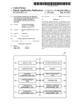
READING OF DEFECT IMAGE DATA
{S201
FOR CREATING CLASSIFICATION STANDARD
CLASSIFICATION BY USER
r8202
AUTOMATIC ADJUSTMENT OF DEFECT
RECOGNITION PARAMETERS
JPSZOZ
EXTRACTION OF CHARACTERISTIC AMOUNTS
AND DETERMINATION OF WEIGHTING
/"S204
I
ADC PROCESSING
K8205
REFLECTION INTO CLASSIFICATION STANDARD DATA fszo?
I
DISPLAY OF SELF-CHECK SCREEN
SELF-CHECK
SELF~CHECKED ADEQUATELY?
5207
[S208
US. Patent
Jan. 7, 2014
Sheet 5 0f 13
US 8,625,906 B2
FIG .7
SELF~GHECK PROCESS
( Start )
GENERATE AND DISPLAY OONFUSION MATRIX
S302
r5301
CELL SELECTED?
DISPLAY DEFECT IMAGE LIST DISPLAY AREA
"8303
S304
DEFECT IMAGE
SELECTED?
DISPLAY OOMPARISON IMAOE IN CORRESPONDING CATEGORY "S306
N0
/
5307
ANALYSIS TAB
SELECTED?
wsasmem
GENERATE AND DISPLAY HISTOORAM
5309
S310
N° /MOVE?
Yes
UPDATE OLASSIFIOATION STANDARD DATA
End
53“
US. Patent
Jan. 7, 2014
Sheet 7 0f 13
US 8,625,906 B2
81
US. Patent
Jan. 7, 2014
Sheet 9 0f 13
US 8,625,906 B2
FIGJ 1
I Start )
IMAGE CAPTURING
AND ADC PROCESSING
READING OF DEFECT IMAGE DATA
/"S40I
S402
CONFIRMATION
r8403
AND RECLASSIFICATION BY UER
REFLECTION INTO
CLASSIFICATION DATA
/S404
GENERATION AND DISPLAY
OF GONFUSION MATRIX
f8405
COPYING AS IMAGE
/"*S407
FOR ADDITIONAL LEARNING
r
UPDATING OF CLASSIFICATION f5408
STANDARD DATA
/
ADC PROCESSING
I
r3409
US. Patent
Jan. 7, 2014
Sheet 10 0f 13
US 8,625,906 B2
FIG.1 2
CHECK PROCESS
(
Start >
IMAGE COMPARISON PROCESS AND CHARACTERISTIC
AMOUNT COMPARISON PROCESS
S502
ANALYSIS 2 TAB
SELECTED?
Yes
5503
CATEGORY SELECTED?
Yes
GENERATION AND DISPLAY OF HISTOGRAM
S504
S505
DEFECT IMAGE
SELECTED?
SIMULATION EXECUTION AND RESULT DISPLAY
r8507
8508
Yes
COPYING OF CORRESPONDING DEFECT IMAGE
5510
N°
APPLY?
Yes
UPDATING OF CLASSIFICATION STANDARD DATA
End
/~S511
US 8,625,906 B2
1
2
IMAGE CLASSIFICATION STANDARD
DISCLOSURE OF INVENTION
UPDATE METHOD, PROGRAM, AND IMAGE
CLASSIFICATION DEVICE
Technical Problem
RELATED APPLICATIONS
In the technology described in Patent Document 1, a clas
si?cation standard for automatic defect classi?cation using a
neural netWork learns based on visual classi?cation by human
eyes. Consequently, if an inspector makes a classi?cation
This application is the US. National Phase under 35 U.S.C.
§37l of International Application No. PCT/J P2009/ 071774,
?led on Dec. 28, 2009, Which in turn claims the bene?t of
error, there may be a contradiction in the classi?cation stan
Japanese Application No. 2008-335779, ?led on Dec. 29,
2008, the disclosures of Which Applications are incorporated
by reference herein.
dard, resulting in a drop in the classi?cation performance for
automatic defect classi?cation. That is, learning is performed
via a neural netWork, based on a classi?cation standard as a
result of visual classi?cation, Which causes problems that a
classi?cation standard With errors is created, and a learning
TECHNICAL FIELD
The present invention relates to a technology of a method
result outputs a result With errors.
Furthermore, in some cases, a desirable classi?cation can
and a program for updating an image classi?cation standard,
and relates to an image classi?cation device.
not be performed, since a defect having one type of charac
teristic may have another type of characteristic if a semicon
BACKGROUND ART
20
During a process of manufacturing semiconductor prod
ucts, it is concerned that short circuit may occur on a formed
circuit pattern because foreign matter or the like is generated,
or a defect such as breaking of Wire, and a defect due to a
problematic of conditions of a manufacturing process, and the
25
like. In order to improve the product yield ratio, it is necessary
tion standard and thereby improving the classi?cation stan
to identify the root cause of such a defect at an early stage and
to take countermeasures. For this purpose, it is necessary to
inspect the semiconductor Wafer for foreign matter adhered
on a Wafer surface and pattern defects formed on the Wafer
ductor-manufacturing process varies after a currently
effective classi?cation standard Was created. That is, it is
necessary to perform learning each time When a defect of a
type that has not been registered in a classi?cation standard is
detected.
The technology described in Patent Document 2 does not
include a technology for updating a once-created classi?ca
30
surface by using a device for inspecting foreign matter on
dard.
The present invention has been developed in vieW of the
foregoing background, and an object of the invention is to
improve a classi?cation standard.
semiconductor Wafers or a visual inspection device for semi
Technical Solution
conductor Wafers, and thereby continuously monitor occur
rence of such defects and take measures to ?nd the causes of
such defects, based on inspection results.
Conventionally, such inspection has been carried out visu
ally by a person. Accordingly, classi?cation of detects of
observation objects is biased, depending on an inspector. In
order to solve this problem, in recent years, technologies for
35
ADR (automatic defect revieW) and ADC (automatic defect
classi?cation), in Which a device automatically performs
determination of the siZe, the shape, the kind, and the like of
40
standard by using an image classi?cation device for classify
ing image data, Wherein a storage section stores classi?cation
standard data in Which information on image data to be a
classi?cation of neWly input image data using the classi?ca
45
on Wafers) by using an SEM (scanning electron microscopy)
revieW device, a system that ef?ciently performs a task While
reducing the Workload of a user is proposed.
As a method for extracting information included in an
inspection image as characteristic amounts and performing
50
automatic classi?cation based on the characteristic amounts,
a method using a neural netWork is disclosed (for example,
refer to Patent Document 1). Further, in order to reduce
effects of inappropriate characteristic amounts on the classi
?cation performance in learning (Weighting of respective
tion standard data is registered, and Wherein, When informa
tion on arbitrary image data is selected via an input section
from the image data registered in the classi?cation data, and
an instruction is input via the input section to additionally
register the selected information on image data into the clas
si?cation standard data, the image classi?cation device addi
tionally registers the selected information on image data into
the classi?cation standard data.
Other solutions Will be described later in embodiments.
Advantageous Effects
55
characteristic amounts) for creating a classi?cation standard
for performing automatic classi?cation, a method that auto
The present invention can improve a classi?cation stan
dard.
BRIEF DESCRIPTION OF THE DRAWINGS
matically selects characteristic amounts that are effective for
classi?cation is disclosed (for example, refer to Patent Docu
ment 2).
standard for classifying image data is registered, and classi
?cation data in Which information on image data as a result of
a defect using an image processing technology, have come to
be introduced. For example, in order to observe, in another
Word, revieW inspected parts (for example, patterns formed
In order to solve the above-described problem, the present
invention is a method for updating an image classi?cation
60
FIG. 1 is a diagram shoWing an example of the con?gura
tion of a semiconductor Wafer manufacturing system in the
present embodiment;
PRIOR ART DOCUMENTS
FIG. 2 is a diagram shoWing the How of data in a semicon
Patent Documents
65
Patent Document 1: JP H08-02l803 A
Patent Document 2: JP 2005-309535 A
ductor Wafer manufacturing system in the present embodi
ment;
FIG. 3 is a diagram shoWing an example of the con?gura
tion of a revieW device in the present embodiment;
US 8,625,906 B2
3
4
FIG. 4 is a diagram showing an example of classi?cation
standard data and classi?cation data;
FIG. 5 is a diagram showing an example of standard char
acteristic amount data and characteristic amount data;
FIG. 6 is a ?owchart showing the procedure of a process for
creating a classi?cation standard in the present embodiment;
FIG. 7 is a ?owchart showing the procedure of a process for
analyZe the defect image data. The SEM review devices 1b
obtain defect image data captured by an electronic micro
scope, and analyZe the defect image data. The appearance
inspection devices 2, the optical review devices 1a, and the
SEM review devices 1b are respectively arranged in plural
number, and plural defect image data can be simultaneously
obtained.
Semiconductor wafers, which are to become products,
self-checking in the present embodiment;
FIG. 8 is a diagram showing an example of a self-check
?ow by lot unit through a plurality of manufacturing devices
4 (FIG. 1). After completion of a process in which appearance
inspection of semiconductor wafers is scheduled in advance,
screen (initial screen) in the present embodiment;
FIG. 9 is a diagram showing an example of a self-check
screen (image comparison) in the present embodiment;
a worker or a conveying machine conveys the semiconductor
FIG. 10 is a diagram showing an example of a self-check
wafers to the appearance inspection device 2, and appearance
screen (characteristic comparison) in the present embodi
ment;
inspection processing is performed. The appearance inspec
tion device 2 captures the images of the appearance of the
FIG. 11 is a ?owchart showing the procedure of a process
executed upon newly obtaining defect image data;
FIG. 12 is a ?owchart showing the procedure of a check
process in the present embodiment;
FIG. 13 is a diagram showing an example of a check screen
20
processing device 3 (S101).
(image comparison) in the present embodiment;
Because the amount of defect data that the appearance
FIG. 14 is a diagram showing an example of a check screen
inspection device 2 outputs is huge, the data processing
(characteristic amount comparison) in the present embodi
ment; and
FIG. 15 is a diagram showing an example of a check screen
device 3 transmits defect data having been ?ltered by a ?lter
25
(simulation) in accordance with the present embodiment.
30
Modes for carrying out the present invention (referred to as
35
images, such as image inspection of foods.
FIG. 1 is a diagram showing an example of the con?gura
40
tor wafers are normally set in a clean room 7 where clean
45
subjected to a conduction test by a probe inspection device 5.
In the clean room 7, there are provided appearance inspec
tion devices 2 for detecting appearance defects of produced
50
55
the review device 1, the probe inspection device 5, and the
data processing device 3 are connected with each other via a
communication line 6.
interface card, a processing section 11 for processing infor
mation, and a storage section 12 for storing information.
The processing section 11 includes a display processing
section 111, an input processing section 112, an automatic
defect classi?cation section 113, a characteristic amount
FIG. 2 is a diagram showing the ?ow of data in the semi
60
embodiment. In FIG. 2, elements same as those in FIG. 1 are
given with the same symbols, and description will be omitted.
The review device 1 includes a plurality of optical review
extraction section 114, and a data obtaining section 115. The
display processing section 111 has a function of processing
information and display the processed information on the
display section 14. The input processing section 112 has a
function of processing the information having been input
devices 111 and a plurality of SEM review devices 1b. The
a digital camera connected with an optical microscope, and
optical review device 1a.
A review device 1 includes an input section 13, such as a
keyboard or a mouse, a display section 14, such as a display,
a transmitting/receiving section 15, such as a communication
processing device 3 that performs processing of image data
having been obtained by the appearance inspection devices 2
optical review devices 111 obtain defect image data, that are
data of defect images on semiconductor wafers, obtained by
FIG. 3 is a diagram showing an example of the con?gura
tion of a review device in the present embodiment. In the
present embodiment, an example is shown where an SEM
review device 1b is assumed to be a review device 1, however,
the invention is not limited thereto, and may be applied to an
reviewing, based on data from the appearance inspection
devices 2. Further, outside the clean room 7, provided is a data
conductor wafer manufacturing system in the present
implemented therein. Information on results of such defect
classi?cation is transmitted as ADR/ADC information via the
review devices 1b).
environment is maintained. Further, semiconductor wafers
or the review devices 1. The appearance inspection device 2,
defects (defect image data) of the semiconductor wafers. The
communication line 6 to the data processing device 3 (S104,
S105). In the present embodiment, described is a technology
related to a review device 1 (optical review devices 1a, SEM
present embodiment.
Manufacturing devices 4 for manufacturing semiconduc
wafers, and review devices 1 (image classi?cation device) for
observation of the appearance defects, in another word,
scope or an electronic microscope, and obtain the images of
the semiconductor wafers at the portions of the detected
optical review devices 111 and the SEM review devices 1b
perform classi?cation of defects by using an ADC function
applicable to systems that perform defect inspection using
manufactured on the line of the manufacturing devices 4 are
determined number of pieces of detect information at ran
dom.
The optical review devices 111 or the SEM review devices
1b capture the images at the coordinate positions according to
the transmitted defect information by using an optical micro
“embodiments”) will be described below, referring to the
tion of a semiconductor wafer manufacturing system in the
function to an optical review devices 111 or an SEM review
devices 1b via the communication line 6 (S102, S103). The
?ltering function includes, for example, extraction of a pre
BEST MODES FOR CARRYING OUT THE
INVENTION
drawings, as appropriate. In the preset embodiment, an
example will be described where an image classi?cation
device is applied to a semiconductor wafer manufacturing
system Z, however, the invention is not limited thereto and is
semiconductor wafers, and if an appearance defect is
detected, the appearance inspection device 2 obtains the coor
dinates of the position of the detected appearance defect as
defect data, and transmits the obtained defect data to the data
65
from the input section 13. The automatic defect classi?cation
section 113 has a function of classifying defect image data by
using ADC. The characteristic amount extraction section 114
has a function of extracting the characteristic amounts of
US 8,625,906 B2
5
6
respective defect image data. The data obtaining section 115
FIG. 5 is a diagram shoWing an example of standard char
acteristic amount data and characteristic amount data. Herein,
the standard characteristic amount data 124 is data created by
has a function of obtaining data from the transmitting/receiv
ing section 15.
The processing section 11 and the respective sections 111
a later-described process With reference to FIG. 6, and the
characteristic amount data 125 is data created by a later
described process With reference to FIG. 11. Although the
standard characteristic amount data 124 and the characteristic
amount data 125 are different from each other in terms of data
to be stored, their formats are the same; therefore, these data
to 115 are realized by executing a program stored in a ROM
(read only memory), not shoWn, or a HD (hard disk), not
shoWn, is loaded into a RAM (random access memory), not
shoWn, by a CPU (central processing unit), not shoWn.
The storage section 12 stores classi?cation standard data
121, classi?cation data 122, a defect image data group 123,
standard characteristic amount data 124, and characteristic
amount data 125. The classi?cation standard data 121, the
classi?cation data 122, the standard characteristic amount
data 124, and the characteristic amount data 125 Will be
described later, referring to FIGS. 4 and 5. The defect image
data group 123 are defect image data captured by the revieW
Will be explained referring to FIG. 5. As shoWn in FIG. 5, the
device 1.
Various Data
FIG. 4 is a diagram shoWing an example of classi?cation
standard data and classi?cation data. Herein, the classi?ca
tion standard data 121 are data created by a process, Which
Will be described later With reference to FIG. 6, and the
classi?cation data 122 are data created by a process, Which
Will be described later With reference to FIG. 1 1. Although the
classi?cation standard data 121 and the classi?cation data
122 are different in terms of stored data, the formats are
5.
similar to each other and Will be commonly described beloW,
referring to FIG. 4.
As shoWn in FIG. 4, the classi?cation standard data 121
and the classi?cation data 122 have a ?eld for categories
standard characteristic amount data 124 and the characteristic
amount data 125 each having a defect image data name have
characteristic amounts of ?atness, brightness, circularity,
size, etc.
The process for creating a classi?cation standard Will be
explained beloW, based on FIG. 6, referring to FIGS. 3, 4 and
FIG. 6 is a ?owchart shoWing the process for creating a
classi?cation standard in the present embodiment. In the pro
20
is a process for creating the classi?cation standard data 121.
25
First, the processing section 11 reads defect image data for
creating a classi?cation standard, from the defect image data
group 123 in the storage section 12 (S201).
Then, the user classi?es the defect image data obtained via
the input section 13 (S202). For example, the user visually
classi?es the defect image data one by one into kinds, such as
particle, scratch, and the like. By the process in S202, initial
classi?cation standard data 121 is created.
30
categorized by user, a ?eld for categories categorized by
In the step of S202, only the column of categories by the
user is ?lled in, While the column of categories by ADC is
blank.
Subsequent to S202, the characteristic amount extraction
ADC, and a ?eld for the names of defect image data. The
categories by user refer to categories classi?ed by a user in
S202 in FIG. 6 (or later-described S403 in FIG. 11). The
categories by ADC are those classi?ed by ADC processing in
cess for creating a classi?cation standard as shoWn in FIG. 6
35
section 114 automatically adjusts defect recognition param
eters (for example, detection sensitivity, noise removing
threshold, protrusion/recession threshold) for extracting
later-described S205 in FIG. 6 (or later-described S401 in
FIG. 11). In the example shoWn in FIG. 4, it is shoWn that
defect image data having been determined to be “C1: par
ticle” by a user and determined to be “C1: particle” also by
characteristic amounts from the defect image data (S203).
Herein, the folloWing operation is performed. In recognizing
a defect portion and extracting a characteristic amount, the
ADC processing are “A1.jpg, A2.jpg, A3.jpg, . . . ”. Further, it 40 characteristic amount extraction section 114 compares nor
is shoWn that there is no defect image data that has been
determined to be “C1: particle” by the user and determined to
mal image data With defect image data, and then extracts the
defect portion. In this state, in order not to erroneously extract
be “C2: scratch” by ADC processing. Further, it is shoWn that
a noise on an image as a defect portion, the characteristic
amount extraction section 114 removes a noise at a certain
defect image data that has been determined to be “C2:
scratch” by the user and determined to be “C1: particle” by
45
level, and in order not to erroneously extract a portion that
appears bright due to light as a defect portion, the character
istic amount extraction section 114 adjusts the detection sen
sitivity. The process in S203 is a technology described in JP
50
be omitted.
ADC processing is “A10.jpg”.
Herein, “C1”, “C2”, and the like are identi?cation numbers
assigned to categories. In the present embodiment, “C1” rep
resents particle, “C2” represents scratch, “C3” represents
pattern short, “C4” represents pattern open, and “C5” repre
2007-198968 A and others, and accordingly description Will
Then, after extracting defect potions, the characteristic
sents no defect. In the present embodiment, these identi?ca
tion numbers Will be used, as appropriate, instead of category
names. In addition to these, it is possible to freely set catego
ries, such as to be critical foreign matter, non-critical foreign
matter, and false information, Without particularly consider
amount extraction section 114 extracts the characteristic
amounts of these defect patterns, and determines hoW to
Weight the extracted characteristic amounts When performing
55
user can freely set category names.
The classi?cation standard data 121 and the classi?cation
data 122 may include data related to every possible combi
nation of categories by a user and by ADC, or may include
only data related to combinations of categories in Which
characteristics, ?atness, brightness, circularity, size, as
described above, and in addition, height, shape, color, texture,
60
defect, background, and the like can be considered. The char
acteristic amount extraction section 114 stores the extracted
characteristic amounts in the storage section 12 as standard
characteristic amount data 124.
corresponding defect image data actually exists. That is, for
example, as shoWn in line 2 in FIG. 4, records having no
corresponding defect image may be omitted. Further, each
defect image data may have a format to Which information of
a category by user and information of a category by ADC are
added.
ADC (S204). Extracting the characteristic amounts means
calculating physical characteristics having been set and quan
ti?ed in advance for each defect image data. As the physical
ing image processing or a characteristic amount. That is, the
Subsequent to S204, the automatic defect classi?cation
65
section 113 performs ADC processing (S205) by using the
characteristic amounts extracted in S204 and the determined
Weight, and classi?es the defect image data by ADC. The
US 8,625,906 B2
7
8
ADC process is a technology described in JP H09-l0l970
“Manual” in FIG. 8), and the respective categories according
and the like, and description in detail will be omitted.
Then, the automatic defect classi?cation section 113
to the classi?cation by ADC (represented by “ADC” in FIG.
8).
Symbols C1 to C5 are, as described above, category iden
re?ects a result of the ADC process into the classi?cation
ti?cation numbers, wherein “C1” represents particle, “C2”
represents scratch, “C3” represents pattern short, “C4” rep
standard data 121 (FIG. 4) (S206). The automatic defect
classi?cation section 113 registers the result of the classi?
cation in S205 into the column, which was blank at the step of
S202, as a category by ADC. More speci?cally, the automatic
defect classi?cation section 113 further classi?es the classi
resents pattem open, and “C5” represents no defect.
In the example in FIG. 8, the vertical axis represents cat
egories according to classi?cation by the user (“Manual”),
and the horizontal axis represents categories according to
classi?cation by ADC.
For example, regarding line 1 of the confusion matrix 211,
?cation made at the step of S202 for more details. For
example, it will be assumed that “A20.jpg”, “A21.jpg”, and
“A22.jpg”, not shown in the drawings, had been determined
to be “C3: pattern short” in S202 (classi?cation by the user),
38 (34+4) defect image data are determined to be C1 (par
ticle) according to the classi?cation (“Manual”) by the user,
however, in S205 (classi?cation by ADC), “A20.jpg” has
while 34 defect image data among them are determined to be
C1 (particle) and 4 defect image data among them are deter
been determined to be “C1: particle”, and “A21.jpg” and
“A22 .jpg” have been determined to be“C3: pattern short”. In
mined to be C3 (pattern short) according to the classi?cation
this case, “A20.jpg” is classi?ed to be “C3: pattern short” as
category determined by the user and to be “C1: particle” as
category by ADC, while “A21.jpg” and “A22.jpg” are classi
20
?ed to be “C3: pattern short” as category by the user, and to be
“C3: pattern short” as category by ADC.
Incidentally, in case that the classi?cation standard data
by ADC. A correct result ratio is the ratio of a classi?cation
result by ADC that agrees with a classi?cation result by user,
to the classi?cation result by the user. For example, the cor
rect result ratio ofline 1 is 34/38><l00589 (%).
Likewise, regarding row 1 in the confusion matrix 211 in
re?ected into the classi?cation standard data 121 and then the
FIG. 8, it is recogniZed that 37 (34+l +2) defect image data are
determined to be C1 (particle) by ADC, while one defect
image data is determined to be C2 (scratch) and two defect
image data are determined to be C5 (no defect) by the user. A
purity ratio is the agreement ratio of a result of classi?cation
by user to a result of classi?cation by ADC. For example, the
purity ratio of row 1 is 34/37><l00592 (%).
The elements having a reference symbol 212 (the central
oblique line) in the confusion matrix 211 represent the num
bers of defect image data in which classi?cation by user
conforms with classi?cation by ADC for the respective cat
egories. Further, symbol 213 represents the ratio of the num
ber of defect image data, in which classi?cation by user
conforms with classi?cation by ADC, to the total number of
all defect image data.
When a matrix button 214 in the input section 13 is selected
and entered, the display processing section 111 counts the
process returns to S203 to extract characteristic amounts. 40
numbers of defect image data in the respective categories,
Then, the display processing section 111 again performs
referring to the classi?cation standard data 121, shown in
FIG. 4, and displays the counted numbers in the confusion
121 is not a type as shown in FIG. 4, but a type in which a
category names are given to each image data, it is merely
25
required to add the category names as a result of classi?cation
in S205 to the corresponding defect image data.
Then, the display processing section 111 displays a self
check screen 200, shown in FIG. 8, on the display section 14
(S207), and the user performs self-check via the self-check
screen 200 (S208). Self-check will be described later, refer
ring to FIGS. 8 to 10.
Then, from a result of the self-check, the user determines as
30
to whether or not the classi?cation of the classi?cation stan
dard data 121 is adequate (S209).
35
As a result of S209, if it is determined to be inadequate
(determined that the classi?cation of the classi?cation stan
dard data 121 is inappropriate) (S209QNo), a change is
ADC processing, and displays a result as a self-check screen.
As a result of S209, if it is determined to be adequate
(determined that the classi?cation of the classi?cation stan
dard data 121 is appropriate) (S209—>Yes), then the process is
terminated.
The procedure of a self-check process will be described
below, based on FIG. 7 and referring to FIG. 3 and FIGS. 8 to
matrix 211.
Herein, the display processing section 111 monitors
45
selected (S302 in FIG. 7).
50
When no cell is selected (S302QNo), the display process
ing section 111 forwards the process to S304. In FIG. 7 and in
FIG. 12, if the process moves forward to the step No. Sm
when no selection input is made in step No. Sn, it means that
55
the processing section 11 determines nothing and executes
the process of the step Sm. This is because, the steps in FIG.
7 and FIG. 12 are actually image processing steps, and each
step is executed when an instruction is input, regardless of the
order of the steps shown in the drawings.
10.
FIG. 7 is a ?owchart showing the process for self-checking
in the present embodiment.
The process, shown in FIG. 7, is a process corresponding to
S207 to S209 in FIG. 6.
First, the display processing section 111 generates a con
fusion matrix 211 (association information between catego
ries), and displays a self-check screen 200a (FIG. 8) includ
If the user selects one of the cells in the confusion matrix
ing the generated confusion matrix 211 (S301).
FIG. 8 is a diagram showing an example of a self-check
screen (initial screen) in the present embodiment.
The self-check screen 20011 (200) includes a confusion
60
matrix display area 201, a defect image list display area 202,
and a defect image con?rmation area 203, which are dis
played in the same window.
In the confusion matrix display area 201, a confusion
matrix 211 is displayed. The confusion matrix 211 is a table
that indicates the numbers of images in the respective catego
ries according to the classi?cation by the user (represented by
whether or not a cell of the confusion matrix 211 has been
65
211 (S302—>Yes, in FIG. 7), then a defect image correspond
ing to the selected cell is displayed in the defect image list
display area 202 (S303 in FIG. 7).
For example, if a cell 215, whose category is C3 (pattern
short) according to classi?cation by user (“Manual”) and is
also C3 (pattern short) according to Classi?cation by ADC, is
selected and entered via the input section 13, then the display
processing section 111 obtains, from the classi?cation stan
dard data 121 in FIG. 4, the names of defect image data stored
in the records of both categories by the user and ADC “C3:
pattern short”. Then, the display processing section 111
US 8,625,906 B2
10
obtains, from the defect image data group 123 (FIG. 3) in the
storage section 12, image data corresponding to the obtained
name of defect image data, and displays the obtained image
obtained defect image data in the comparison image display
data in the defect image list display area 202.
Incidentally, in FIG. 8, as “12” is described in cell 215, the
A characteristic amount display area 400 (FIG. 10) is hid
den at the back of the image comparison area 320, and the
number of images displayed in the defect image list display
characteristic amount display area 400 (FIG. 10) is displayed
area 202 is also 12. The user can refer to 12 images by moving
the slide bar in the defect image list display area 202 shoWn in
FIG. 8.
section 13.
area 340 as comparison images in the corresponding category
(S306 in FIG. 7).
in front by selectively inputting “analysis tab” via the input
That is, the display processing section 111 determines
Whether or not “analysis tab” has been selectively input (se
lected) (S307 in FIG. 7), and if the analysis tab has not been
selected (S307—>No), the display processing section 111 pro
In the defect image con?rmation area 203, nothing is dis
played at the step of S303. A save button 205 and a delete
button 206 Will be described later.
In order to create accurate classi?cation standard data 121
ceeds the process to S310 in FIG. 7.
If the analysis tab has been selected (S307—>Yes), then the
and thereby improve the accuracy of classi?cation by ADC, it
display processing section 111 displays the characteristic
is necessary to improve the purity ratio and the correct result
ratio in the confusion matrix 211.
A method for updating the classi?cation standard data 121
for improving the purity ratio and the correct result ratio Will
be described beloW, referring to FIGS. 9 and 10. Incidentally,
amount display area 400 shoWn in FIG. 10.
FIG. 10 is a diagram shoWing an example of a self-check
screen (for comparing characteristic amounts) according to
20
in FIGS. 9 and 10, elements that are similar to those in FIG. 8
are given With the same symbols, and description Will be
omitted.
FIG. 9 is a diagram shoWing an example of a self-check
screen (image comparison) according to the present embodi
self-check screen 2000 (200), to the characteristic amount
display area 400, then the dragged and dropped defect image
40111 is copied and displayed in the characteristic amount
25
not a category Whose characteristic amounts the user intends
In FIG. 9, an example is shoWn Where, in the confusion
to display has been selected via a characteristic amount selec
matrix 211, a cell 301 Whose classi?cation by user
30
cessing section 111 proceeds the process to S307 in FIG. 7.
If the user drags and drops a defect image 31111 from defect
images displayed in the defect image list display area 202 to
the defect image con?rmation area 203 (S304—>Yes, in FIG.
7), then the dragged and dropped defect image 31111 is copied
to an object image display area 330 in a image comparison
area 320 in the defect image con?rmation area 203, and
enlarged and displayed as a defect image 3111).
Further, in a comparison image display area 340, defect
images 342, Which belong to a category selected via a cat
egory selection pull-doWn menu 341, are displayed. A cat
egory Which is selected via the category selection pull-doWn
menu 341 is a category according to classi?cation by user. If
the user Wishes to compare images in a category With images
in another category, the user selects said another category by
tion pull-doWn-menu 402, 403 (S308 in FIG. 7), and if not
selected (S308—>No), the display processing section 111 pro
ceeds the process to S310 in FIG. 7.
If a category Whose characteristic amounts the user intends
to display has been selected via the characteristic amount
The display processing section 111 determines Whether or
not a defect image displayed in the defect image list display
area 202 has been selected (S304 in FIG. 7). If no defect
image has been selected (S304QNo), then the display pro
display area 400 as a defect image 4011).
The display processing section 111 determines Whether or
ment.
(“Manual”) is “C1: particle” and Whose classi?cation by
ADC (“ADC”) is “C3: pattern short” is selectively input.
the present embodiment.
If the user drags and drops an arbitrary defect image 401a
displayed in the defect image list display area 202 on the
35
selection pull-doWn-menu 402, 403 (S308—>Yes, in FIG. 7),
then the display processing section 111 generates a histogram
representing the distribution of the respective characteristic
amounts in the selected category, and displays the generated
histogram in a characteristic amount distribution display area
40
411 (S309 in FIG. 7). A category selected via the character
istic amount selection pull-doWn-menu 402, 403 is a category
classi?ed by user.
45
In graphs displayed in the characteristic amount distribu
tion display area 411, the horiZontal axis represents the values
of respective characteristic amounts and the vertical axis rep
resents the numbers of defect image data With the respective
values. In the characteristic amount distribution display area
411, the characteristic amount distribution of a category
selected via the characteristic amount selection pull-doWn
50
menu 402 is displayed as a holloW histogram, and the char
acteristic amount distribution of a category selected via the
using the category selection pull-doWn-menu 341 via the
input section 13.
More speci?cally, the display processing section 111 deter
characteristic amount selection pull-doWn-menu 403 is dis
played as a hatched histogram. Further, a portion Where the
mines Whether or not a category has been selected by the
the characteristic amount selection pull-doWn-menu 402 and
category selection pull-doWn-menu 341 (S305 in FIG. 7). If
no category has been selected (S305QNo), then the display
processing section 111 proceeds the process to S307.
If a category is selected by the category selection pull
doWn-menu 341 (S305QYes, in FIG. 7), then the display
processing section 111 refers to the classi?cation standard
data 121 in FIG. 4, With a key of the selected category, and
thereby obtains the names of defect image data stored in all
records corresponding to the selected category With classi?
cation by user. Then, the display processing section 111
obtains defect image data corresponding to the obtained
names of defect image data from the defect image data group
123 (FIG. 3) in the storage section 12, and displays the
characteristic amount distribution of a category selected via
55
the characteristic amount distribution of a category selected
60
via the characteristic amount selection pull-doWn-menu 403
overlap With each other is displayed as a black solid histo
gram. In the example, shoWn in FIG. 10, the characteristic
amount distribution of “C1: particle” is displayed by a holloW
histogram, and the characteristic amount distribution of “C2:
65
scratch” is displayed by a hatched histogram. The percentage
displayed in the right top portion of a characteristic amount
distribution display area 411 represents the separation degree
that is the ratio of the non-overlapped distribution portion to
the entire characteristic distribution in tWo categories. That is,
the percentage represents the ratio of the histograms Which
are not black-solid to the entire characteristic amount distri
US 8,625,906 B2
11
12
bution. It is shown that if the separation degree is larger, the
(S310 in FIG. 7), and if not to move (S310QNo), the pro
cessing section 11 terminates the process. Herein, “not to
difference is the greater between the characteristic amount
distributions of two categories.
move” refers to a case, for example, where a delete button 206
is selected and entered, or the user closes the self-check
A histogram representing characteristic amount distribu
tion is created in the following procedure. First, the display
screen 200 in a state that the move button 332 has not been
selected and entered. Incidentally, S310 corresponds to the
processing section 111 searches a category by the user in the
classi?cation standard data 121 in FIG. 4 by using the cat
process in S209 in FIG. 6.
If the user intends to move the current defect image from
the current category to another category, the user selects a
egory name selected via the characteristic amount selection
pull-down-menu 402 as a key, and obtains the names of defect
image data included in all corresponding records.
Then, the display processing section 111 searches in the
moving destination category via a moving-destination-cat
standard characteristic amount data 124 in FIG. 5 by using the
of the respective characteristic amounts corresponding to the
defect image data names, and counts the number of defect
the move button 332 (FIG. 9) (S310—>Yes, in FIG. 7), and
thereupon the display processing section 111 moves the data
name of the defect image 311!) displayed in the object image
display area 330 (FIG. 9) to the selected moving destination
image data with the same characteristic amount on each indi
category. More speci?cally, the display processing section
vidual characteristic. For example, in the example in FIG. 5,
assuming that “A1 .jpg” and “A2.jpg” are objects of process
ing, the display processing section 111 ?rst refers to record
“A1.jpg” and counts “?atness: 50” by +1, and counts “bright
ness: 60” by +1. The display processing section 111 likewise
111 moves the name of the defect image data corresponding
to the defect image 3111) to a record of the selected moving
destination category selected by the user in the classi?cation
egory selection pull-down menu 331 and selects and enters
obtained defect image data names as a key, refers to the values
20
counts “circularity” and “siZe” of this record as well.
Then, the display processing section 111 refers to record
“A2.jpg”, and counts “?atness: 40” by + 1, and counts “bright
ness: 60” by +1 (“brightnessz 60” thereby becomes “2”). The
display area 330 is an inappropriate (for example, a case
25
display processing section 111 likewise counts “circularity”
and “size” of this record as well.
The display processing section 111 performs this process
on all the obtained names of defect image data, thereafter
further performs the same process also on the category
selected via the characteristic amount selection pull-down
menu 403, and calculates the histograms of characteristic
amounts for the respective characteristics.
Further, bars 412 in the characteristic amount distribution
display area 411 represent the respective values of the char
acteristic amounts of the defect image 4011). The display
processing section 111 obtains the values of characteristic
where the image of a defect is not correctly captured) image
for creating the classi?cation standard data 121, then the
delete button 206 is selected and entered via the input section
13, and thereupon, the display processing section 111 can
delete the name of this defect image data from the classi?ca
tion standard data 121.
30
When the user has moved a defect image data name to be
used for learning to another category by selecting and enter
ing the move button 332 (FIG. 9), when the user has deleted
defect image data from the classi?cation standard data 121 by
selecting and entering the delete button 206, or when the user
35
has switched effectiveness/ineffectiveness of a characteristic
amount to be used forADC processing, it is possible to update
the confusion matrix 211 by selecting and entering the matrix
button 214 each time. Further, the classi?cation standard data
amounts from the standard characteristic amount data 124 in
FIG. 5, by using the name of the defect image data of the
defect image 4011) as a key, and displays bars 412 at positions
representing the respective characteristic amounts corre
standard data 121, and thereby updates the classi?cation stan
dard data 121 (S311 in FIG. 7).
Further, if a defect image displayed in the object image
121 in this state can be overwritten or saved with another
40
name by selecting and entering the save button 205.
The classi?cation standard data 121 having been created in
sponding to the values obtained by the display processing
such a manner is used as a classi?cation standard for ADC
section 111.
processing in the review device 1, and the review device 1
automatically classi?es defects on semiconductor wafers and
transfers identi?cation numbers of categories in respective
results to the data processing device 3. On the other hand, the
defect image data group 123 determined to be defect images
byADC is stored in the storage section 12 of the review device
1 for respective wafers.
Through the process up to here, a classi?cation standard
data 121 has been created and adjusted for classi?cation of
defect images by ADC. A process to be performed when new
defect image data is transmitted to the review device 1 after
the classi?cation standard data 121 is created will be
described below, referring to FIGS. 10 to 14. The transmitted
new defect image data is stored in the defect image data group
123 in the storage section 12.
In a separation degree list display area 431, the above
described separation degrees are listed in the descending
45
order.
Radio buttons 421, 422 are used to indicate characteristic
amounts which are currently used in performing classi?ca
tion by ADC processing. In the example in FIG. 10, “?at
ness”, “brightness”, and “circularity”, for which the radio
50
buttons 421, 422 are “ON”, are characteristic amounts which
are currently used in the ADC process. By switching “On/
Off ’ of the radio buttons 421, 422, the user can set effective
ness/ineffectiveness of characteristic amounts to be used in
the ADC process. For example, when the user determines that
55
“brightness” and “circularity” are ineffective characteristic
amounts, the user can set the usage of these characteristic
amounts in the ADC process to be ineffective by selecting and
entering the corresponding radio buttons 412, 422. Further,
on the contrary, when the user determines that “size” is valid
characteristic amount, the user can set the usage of this char
acteristic amount in the ADC process to be effective by select
60
ing and entering the corresponding radio buttons 421, 422.
FIG. 11 is a ?owchart showing the process executed when
defect image data is obtained anew.
First, when the review device 1 captures new defect image
data after the process in FIG. 6, the characteristic amount
extraction section 114 automatically adjusts the defect rec
ognition parameters, thereafter extracts characteristic
amounts, and the automatic defect classi?cation section 113
By determining whether or not a move button 332 (FIG. 9)
111 determines whether or not to move corresponding defect
performs ADC processing of the captured defect image data
(S401) and thereby classi?es defect images. A result of ADC
image data from the current category to another category
processing is registered in the classi?cation data 122 shown in
has been selected and entered, the display processing section
65