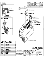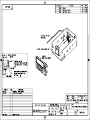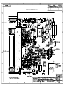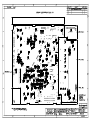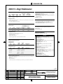
1
Model 2000 Multimeter
Repair Manual
A GREATER MEASURE OF CONFIDENCE
WARRANTY
Keithley Instruments, Inc. warrants this product to be free from defects in material and workmanship for a
period of 3 years from date of shipment.
Keithley Instruments, Inc. warrants the following items for 90 days from the date of shipment: probes, cables,
rechargeable batteries, diskettes, and documentation.
During the warranty period, we will, at our option, either repair or replace any product that proves to be defective.
To exercise this warranty, write or call your local Keithley representative, or contact Keithley headquarters in
Cleveland, Ohio. You will be given prompt assistance and return instructions. Send the product, transportation
prepaid, to the indicated service facility. Repairs will be made and the product returned, transportation prepaid.
Repaired or replaced products are warranted for the balance of the original warranty period, or at least 90 days.
LIMITATION OF WARRANTY
This warranty does not apply to defects resulting from product modification without Keithley’s express written
consent, or misuse of any product or part. This warranty also does not apply to fuses, software, non-rechargeable
batteries, damage from battery leakage, or problems arising from normal wear or failure to follow instructions.
THIS WARRANTY IS IN LIEU OF ALL OTHER WARRANTIES, EXPRESSED OR IMPLIED, INCLUDING
ANY IMPLIED WARRANTY OF MERCHANTABILITY OR FITNESS FOR A PARTICULAR USE. THE
REMEDIES PROVIDED HEREIN ARE BUYER’S SOLE AND EXCLUSIVE REMEDIES.
NEITHER KEITHLEY INSTRUMENTS, INC. NOR ANY OF ITS EMPLOYEES SHALL BE LIABLE FOR
ANY DIRECT, INDIRECT, SPECIAL, INCIDENTAL OR CONSEQUENTIAL DAMAGES ARISING OUT
OF THE USE OF ITS INSTRUMENTS AND SOFTWARE EVEN IF KEITHLEY INSTRUMENTS, INC., HAS
BEEN ADVISED IN ADVANCE OF THE POSSIBILITY OF SUCH DAMAGES. SUCH EXCLUDED DAMAGES SHALL INCLUDE, BUT ARE NOT LIMITED TO: COSTS OF REMOVAL AND INSTALLATION,
LOSSES SUSTAINED AS THE RESULT OF INJURY TO ANY PERSON, OR DAMAGE TO PROPERTY.
Keithley Instruments, Inc.
28775 Aurora Road • Cleveland, Ohio 44139 • 440-248-0400 • Fax: 440-248-6168
1-888-KEITHLEY (534-8453) • www.keithley.com
Sales Offices:
Bergensesteenweg 709 • B-1600 Sint-Pieters-Leeuw • 02-363 00 40 • Fax: 02/363 00 64
Yuan Chen Xin Building, Room 705 • 12 Yumin Road, Dewai, Madian • Beijing 100029 • 8610-6202-2886 • Fax: 8610-6202-2892
Tietäjäntie 2 • 02130 Espoo • Phone: 09-54 75 08 10 • Fax: 09-25 10 51 00
3, allée des Garays • 91127 Palaiseau Cédex • 01-64 53 20 20 • Fax: 01-60 11 77 26
Landsberger Strasse 65 • 82110 Germering • 089/84 93 07-40 • Fax: 089/84 93 07-34
Unit 2 Commerce Park, Brunel Road • Theale • Berkshire RG7 4AB • 0118 929 7500 • Fax: 0118 929 7519
Flat 2B, Willocrissa • 14, Rest House Crescent • Bangalore 560 001 • 91-80-509-1320/21 • Fax: 91-80-509-1322
Viale San Gimignano, 38 • 20146 Milano • 02-48 39 16 01 • Fax: 02-48 30 22 74
New Pier Takeshiba North Tower 13F • 11-1, Kaigan 1-chome • Minato-ku, Tokyo 105-0022 • 81-3-5733-7555 • Fax: 81-3-5733-7556
2FL., URI Building • 2-14 Yangjae-Dong • Seocho-Gu, Seoul 137-888 • 82-2-574-7778 • Fax: 82-2-574-7838
Postbus 559 • 4200 AN Gorinchem • 0183-635333 • Fax: 0183-630821
c/o Regus Business Centre • Frosundaviks Allé 15, 4tr • 169 70 Solna • 08-509 04 679 • Fax: 08-655 26 10
Kriesbachstrasse 4 • 8600 Dübendorf • 01-821 94 44 • Fax: 01-820 30 81
1FL., 85 Po Ai Street • Hsinchu, Taiwan, R.O.C. • 886-3-572-9077• Fax: 886-3-572-9031
BELGIUM:
CHINA:
FINLAND:
FRANCE:
GERMANY:
GREAT BRITAIN:
INDIA:
ITALY:
JAPAN:
KOREA:
NETHERLANDS:
SWEDEN:
SWITZERLAND:
TAIWAN:
4/02
Model 2000 Multimeter
Repair Manual
©1995, Keithley Instruments, Inc.
All rights reserved.
Cleveland, Ohio, U.S.A.
Second Printing, March 1997
Document Number: 2000-902-01 Rev. B
Manual Print History
The print history shown below lists the printing dates of all Revisions and Addenda created
for this manual. The Revision Level letter increases alphabetically as the manual undergoes subsequent updates. Addenda, which are released between Revisions, contain important change information that the user should incorporate immediately into the manual. Addenda are numbered
sequentially. When a new Revision is created, all Addenda associated with the previous Revision
of the manual are incorporated into the new Revision of the manual. Each new Revision includes
a revised copy of this print history page.
Revision A (Document Number 2000-902-01) ................................................................. May 1995
Revision B (Document Number 2000-902-01) .............................................................. March 1997
All Keithley product names are trademarks or registered trademarks of Keithley Instruments, Inc.
Other brand names are trademarks or registered trademarks of their respective holders.
Safety Precautions
The following safety precautions should be observed before using this product and any associated instrumentation. Although
some instruments and accessories would normally be used with non-hazardous voltages, there are situations where hazardous
conditions may be present.
This product is intended for use by qualified personnel who recognize shock hazards and are familiar with the safety precautions
required to avoid possible injury. Read and follow all installation, operation, and maintenance information carefully before using the product. Refer to the manual for complete product specifications.
If the product is used in a manner not specified, the protection provided by the product may be impaired.
The types of product users are:
Responsible body is the individual or group responsible for the use and maintenance of equipment, for ensuring that the equipment is operated within its specifications and operating limits, and for ensuring that operators are adequately trained.
Operators use the product for its intended function. They must be trained in electrical safety procedures and proper use of the
instrument. They must be protected from electric shock and contact with hazardous live circuits.
Maintenance personnel perform routine procedures on the product to keep it operating properly, for example, setting the line
voltage or replacing consumable materials. Maintenance procedures are described in the manual. The procedures explicitly state
if the operator may perform them. Otherwise, they should be performed only by service personnel.
Service personnel are trained to work on live circuits, and perform safe installations and repairs of products. Only properly
trained service personnel may perform installation and service procedures.
Keithley products are designed for use with electrical signals that are rated Installation Category I and Installation Category II,
as described in the International Electrotechnical Commission (IEC) Standard IEC 60664. Most measurement, control, and data
I/O signals are Installation Category I and must not be directly connected to mains voltage or to voltage sources with high transient over-voltages. Installation Category II connections require protection for high transient over-voltages often associated with
local AC mains connections. Assume all measurement, control, and data I/O connections are for connection to Category I sources unless otherwise marked or described in the Manual.
Exercise extreme caution when a shock hazard is present. Lethal voltage may be present on cable connector jacks or test fixtures.
The American National Standards Institute (ANSI) states that a shock hazard exists when voltage levels greater than 30V RMS,
42.4V peak, or 60VDC are present. A good safety practice is to expect that hazardous voltage is present in any unknown
circuit before measuring.
Operators of this product must be protected from electric shock at all times. The responsible body must ensure that operators
are prevented access and/or insulated from every connection point. In some cases, connections must be exposed to potential
human contact. Product operators in these circumstances must be trained to protect themselves from the risk of electric shock.
If the circuit is capable of operating at or above 1000 volts, no conductive part of the circuit may be exposed.
Do not connect switching cards directly to unlimited power circuits. They are intended to be used with impedance limited sources. NEVER connect switching cards directly to AC mains. When connecting sources to switching cards, install protective devices to limit fault current and voltage to the card.
Before operating an instrument, make sure the line cord is connected to a properly grounded power receptacle. Inspect the connecting cables, test leads, and jumpers for possible wear, cracks, or breaks before each use.
When installing equipment where access to the main power cord is restricted, such as rack mounting, a separate main input power disconnect device must be provided, in close proximity to the equipment and within easy reach of the operator.
For maximum safety, do not touch the product, test cables, or any other instruments while power is applied to the circuit under
test. ALWAYS remove power from the entire test system and discharge any capacitors before: connecting or disconnecting ca5/02
bles or jumpers, installing or removing switching cards, or making internal changes, such as installing or removing jumpers.
Do not touch any object that could provide a current path to the common side of the circuit under test or power line (earth) ground. Always make measurements with dry hands while standing on a dry, insulated surface capable of withstanding the voltage being measured.
The instrument and accessories must be used in accordance with its specifications and operating instructions or the safety of the
equipment may be impaired.
Do not exceed the maximum signal levels of the instruments and accessories, as defined in the specifications and operating information, and as shown on the instrument or test fixture panels, or switching card.
When fuses are used in a product, replace with same type and rating for continued protection against fire hazard.
Chassis connections must only be used as shield connections for measuring circuits, NOT as safety earth ground connections.
If you are using a test fixture, keep the lid closed while power is applied to the device under test. Safe operation requires the use
of a lid interlock.
If
The
or
!
is present, connect it to safety earth ground using the wire recommended in the user documentation.
symbol on an instrument indicates that the user should refer to the operating instructions located in the manual.
The
symbol on an instrument shows that it can source or measure 1000 volts or more, including the combined effect of
normal and common mode voltages. Use standard safety precautions to avoid personal contact with these voltages.
The WARNING heading in a manual explains dangers that might result in personal injury or death. Always read the associated
information very carefully before performing the indicated procedure.
The CAUTION heading in a manual explains hazards that could damage the instrument. Such damage may invalidate the warranty.
Instrumentation and accessories shall not be connected to humans.
Before performing any maintenance, disconnect the line cord and all test cables.
To maintain protection from electric shock and fire, replacement components in mains circuits, including the power transformer,
test leads, and input jacks, must be purchased from Keithley Instruments. Standard fuses, with applicable national safety approvals, may be used if the rating and type are the same. Other components that are not safety related may be purchased from
other suppliers as long as they are equivalent to the original component. (Note that selected parts should be purchased only
through Keithley Instruments to maintain accuracy and functionality of the product.) If you are unsure about the applicability
of a replacement component, call a Keithley Instruments office for information.
To clean an instrument, use a damp cloth or mild, water based cleaner. Clean the exterior of the instrument only. Do not apply
cleaner directly to the instrument or allow liquids to enter or spill on the instrument. Products that consist of a circuit board with
no case or chassis (e.g., data acquisition board for installation into a computer) should never require cleaning if handled according to instructions. If the board becomes contaminated and operation is affected, the board should be returned to the factory for
proper cleaning/servicing.
Table of Contents
1 Routine Maintenance
Introduction..........................................................................................1-2
Setting line voltage and replacing fuse ................................................1-2
AMPS fuse replacement ......................................................................1-4
2 Troubleshooting
Introduction..........................................................................................2-2
Repair considerations...........................................................................2-3
Power-on test .......................................................................................2-3
Front panel tests...................................................................................2-4
Principles of operation.........................................................................2-5
Display board checks.........................................................................2-11
Power supply checks..........................................................................2-11
Digital circuitry checks......................................................................2-12
Analog signal switching states...........................................................2-13
Built-In Test overview .......................................................................2-18
Built-In Test documentation ..............................................................2-22
3 Disassembly
Introduction..........................................................................................3-2
Handling and cleaning .........................................................................3-3
Static sensitive devices ........................................................................3-4
Assembly drawings..............................................................................3-4
Case cover removal..............................................................................3-5
Changing trigger link lines ..................................................................3-6
Motherboard removal ..........................................................................3-7
Front panel disassembly ......................................................................3-8
Main CPU firmware replacement ........................................................3-9
Removing power components ...........................................................3-10
Instrument re-assembly......................................................................3-12
4 Replaceable Parts
Introduction..........................................................................................4-2
Parts lists ..............................................................................................4-2
Ordering information ...........................................................................4-2
Factory service.....................................................................................4-3
Component layouts ..............................................................................4-3
A Specifications
............................................................................................................A-1
List of Illustrations
1 Routine Maintenance
Power module...................................................................................... 1-3
2 Troubleshooting
Power supply block diagram ............................................................... 2-6
Digital circuitry block diagram ........................................................... 2-7
Analog circuitry block diagram........................................................... 2-9
3 Disassembly
Trigger link line connections............................................................... 3-6
List of Tables
1 Routine Maintenance
Fuse rating ...........................................................................................1-3
2 Troubleshooting
Power supply circuits...........................................................................2-7
Display board checks.........................................................................2-11
Power supply checks..........................................................................2-11
Digital circuitry checks......................................................................2-12
DCV signal switching........................................................................2-13
ACV and FREQ signal switching ......................................................2-13
Ω2 signal switching ...........................................................................2-14
Ω4 signal switching ...........................................................................2-14
Ω2/Ω4 reference switching................................................................2-15
DCA signal switching........................................................................2-15
ACA signal switching ........................................................................2-15
DCV signal multiplexing and gain ....................................................2-16
ACV and ACA signal multiplexing and gain.....................................2-16
DCA signal multiplexing and gain ....................................................2-16
Ω2 signal multiplexing and gain........................................................2-16
Ω4 signal multiplexing and gain........................................................2-17
Circuit section location for switching devices...................................2-17
Built-In Test summary .......................................................................2-19
1
Routine
Maintenance
1-2
Routine Maintenance
Introduction
The information in this section deals with routine type maintenance that can be performed by
the operator. This information is arranged as follows:
•
•
Setting line voltage and replacing fuse — Explains how to select the alternate power line
voltage setting, and how to replace a blown power line fuse.
Amps fuse replacement — Explains how to replace a blown current fuse.
Setting line voltage and replacing fuse
A rear panel fuse located next to the AC receptacle (in the power module) protects the power
line input of the instrument. If the line voltage setting needs to be changed or the line fuse needs
to be replaced, perform the following steps.
WARNING
Disconnect the line cord at the rear panel and remove all test leads connected to the instrument (front and rear) before replacing the line fuse or changing the line voltage setting.
1.
Place the tip of a flat-blade screwdriver into the power module by the fuse holder assembly (see Figure 1-1). Gently push in and to the left. Release pressure on the assembly and
its internal spring will push it out of the power module.
2.
Remove the fuse and replace it with the type listed in Table 1-1.
CAUTION
3.
4.
For continued protection against fire or instrument damage, only replace
fuse with the type and rating listed. If the instrument repeatedly blows fuses,
locate and correct the cause of the trouble before replacing the fuse.
If configuring the instrument for a different line voltage, remove the line voltage selector
from the assembly and rotate it to the proper position. When the selector is installed into
the fuse holder assembly, the correct line voltage appears inverted in the window.
Install the fuse holder assembly into the power module by pushing it in until it locks in
place.
Routine Maintenance
Figure 1-2
Power module
Model 2000
WARNING:NO INTERNAL OPERATOR SERVICABLE PARTS,SERVICE BY QUALIFIED PERSONNEL ONLY.
HI
MADE IN
U.S.A.
IEEE-488
350V
PEAK
!
1000V
PEAK
(CHANGE IEEE ADDRESS
FROM FRONT PANEL)
TRIGGER
LINK
RS232
!
LO
SENSE
Ω 4W
500V
INPUT PEAK
1
2
3
4
5
6
VMC
EXT TRIG
!
FUSE
LINE
250mAT
(SB)
100 VAC
120 VAC
125mAT
(SB)
220 VAC
240 VAC
LINE RATING
120
!
50, 60
400HZ
17 VA MAX
Line Voltage Selector
CAUTION:FOR CONTINUED PROTECTION AGAINST FIRE HAZARD,REPLACE FUSE WITH SAME TYPE AND RATING.
Fuse
100
220
240
120
Spring
Window
Fuse Holder Assembly
Table 1-1
Fuse rating
Line voltage
Fuse rating
Keithley part no.
100/120V
220/240V
0.25A slow-blow 5×20mm
0.125A slow-blow 5×20mm
FU-96-4
FU-91
1-3
1-4
Routine Maintenance
AMPS fuse replacement
WARNING
Make sure the instrument is disconnected from the power line and other equipment before
replacing the AMPS fuse.
1.
2.
Turn off the power and disconnect the power line and test leads.
From the front panel, gently push in the AMPS jack with your thumb and rotate the fuse
carrier one-quarter turn counter-clockwise. Release pressure on the jack and its internal
spring will push the fuse carrier out of the socket.
3.
Remove the fuse and replace it with the same type 3A, 250V, fast blow: Keithley
part number FU-99-1.
CAUTION
4.
Do not use a fuse with a higher current rating than specified or instrument
damage may occur. If the instrument repeatedly blows fuses, locate and correct the cause of the trouble before replacing the fuse.
Install the new fuse by reversing the procedure.
2
Troubleshooting
2-2
Troubleshooting
Introduction
WARNING
The information in this section is intended for qualified service personnel.
Some of these procedures may expose you to hazardous voltages. Do not perform these hazardous procedures unless you are qualified to do so.
This section of the manual will assist you in troubleshooting the Model 2000. Included are
self-tests, test procedures, troubleshooting tables, and circuit descriptions. It is left to the discretion of the repair technician to select the appropriate tests and documentation needed to troubleshoot the instrument. This section is arranged as follows:
•
•
•
•
•
•
•
•
•
•
Repair considerations — Covers some considerations that should be noted before making any repairs to the Model 2000.
Power-on test — Describes the tests that are performed on memory elements each time
the instrument is turned on.
Front panel tests — Provides the procedures to test the functionality of the front panel
keys and the display.
Principles of operation — Provides support documentation for the various troubleshooting tests and procedures. Included is some basic circuit theory for the display board,
power supply, digital circuitry and analog circuitry.
Display board checks — Provides display board checks that can be made if front panel
tests fail.
Power supply checks — Provides power supply checks that can be made if the integrity
of the power supply is questionable.
Digital circuitry checks — Provides some basic checks for the digital circuitry.
Analog signal switching states — Provides tables to check switching states of various
relays, FETs, analog switches and the A/D multiplexer for the basic measurement functions and ranges.
Built-in test overview — Summarizes the built-in tests, which can be used to test and exercise the various digital and analog circuits.
Built-in test documentation — Provides a detailed analysis of each built-in test.
Troubleshooting
2-3
Repair considerations
Before making any repairs to the Model 2000, be sure to read the following considerations.
CAUTION
1.
2.
3.
4.
5.
The PC-boards are built using surface mount techniques and require specialized equipment and skills for repair. If you are not equipped and/or qualified,
it is strongly recommended that you send the unit back to the factory for repairs or limit repairs to the PC-board replacement level. Without proper
equipment and training, you could damage a PC-board beyond repair.
Repairs will require various degrees of disassembly. However, it is recommended that
the Front Panel Tests and Built-In-Test be performed prior to any disassembly. The disassembly instructions for the Model 2000 are contained in Section 3 of this manual.
Do not make repairs to surface mount PC-boards unless equipped and qualified to do so
(see previous CAUTION).
When working inside the unit and replacing parts, be sure to adhere to the handling precautions and cleaning procedures explained in Section 3.
Many CMOS devices are installed in the Model 2000. These static-sensitive devices require special handling as explained in Section 3.
Anytime a circuit board is removed or a component is replaced, the Model 2000
must be recalibrated.
Power-on test
During the power-on sequence, the Model 2000 will perform a checksum test on its EPROM
(U156 and U157) and test its RAM (U151 and U152). If one of these tests fails the instrument
will lock up.
2-4
Troubleshooting
Front panel tests
There are two front panel tests: one to test the functionality of the front panel keys and one to
test the display. In the event of a test failure, refer to “Display Board Checks” for details on troubleshooting the display board.
KEY test
The KEY test allows you to check the functionality of each front panel key. Perform the following steps to run the KEY test:
1.
2.
3.
Press SHIFT and then TEST to access the self-test options.
Use the ▲ or ▼ key to display “TEST: KEY”.
Press ENTER to start the test. When a key is pressed, the label name for that key is displayed to indicate that it is functioning properly. When the key is released, the message
“NO KEY PRESS” is displayed.
4.
Pressing EXIT tests the EXIT key. However, the second consecutive press of EXIT
aborts the test and returns the instrument to normal operation.
DISP test
The display test allows you to verify that each pixel and annunciator in the vacuum fluorescent display is working properly. Perform the following steps to run the display test:
1.
2.
3.
Press SHIFT and then TEST to access the self-test options.
Use the ▲ or ▼ key to display “TEST: DISP”.
Press ENTER to start the test. There are four parts to the display test. Each time ENTER
is pressed, the next part of the test sequence is selected. The four parts of the test sequence are as follows:
A. All annunciators are displayed.
B. The pixels of each digit are sequentially displayed.
C. The 12 digits (and annunciators) are sequentially displayed.
D. The annunciators located at either end of the display are sequentially displayed.
4.
When finished, abort the display test by pressing EXIT. The instrument returns to
normal operation.
Troubleshooting
2-5
Principles of operation
The following information is provided to support the troubleshooting tests and procedures
covered in this section of the manual. Refer to the following block diagrams:
Block Diagrams:
Figure 2-1 — Power supply block diagram
Figure 2-2 — Digital circuitry block diagram
Figure 2-3 — Analog circuitry block diagram
Display board
Microcontroller
U401 is the display board microcontroller that controls the display and interprets key data.
The microcontroller uses three internal, peripheral I/O ports for the various control and read
functions.
Display data is serially transmitted to the microcontroller from the digital section via the TXB
line to the microcontroller RDI terminal. In a similar manner, key data is serially sent back to
the digital section through the RXB line via TDO. The 4MHz clock for the microcontroller is
generated by crystal Y401.
Display
DS401 is the display module, which can display up to 12 alpha-numeric characters and the
various annunciators.
The display uses a common multiplexing scheme with each character refreshed in sequence.
U402 and U403 are the drivers for the display characters and annunciators. Note that data for
the drivers are serially transmitted from the microcontroller (MOSI and PC1).
Filament voltage for the display is derived from the power supply transformer (F1 and F2).
The display drivers require +37VDC and +5VDC, which are supplied by U144 (+5VD) and
U101 (+37V).
2-6
Troubleshooting
Key matrix
The front panel keys (S401-S430) are organized into a row-column matrix to minimize the
number of microcontroller peripheral lines required to read the keyboard. A key is read by strobing the columns and reading all rows for each strobed column. Key down data is interpreted by
the display microcontroller and sent back to the main microprocessor using proprietary encoding schemes.
Power supply
The following information provides some basic circuit theory that can be used as an aid to
troubleshoot the power supply. A block diagram of the power supply is shown in Figure 2-1.
Figure 2-1
Power supply
block diagram
CR104
C128, C156
U144
CR116, CR117
C104, C108
U101
Fuse
Power
Switch
Line
Voltage
Switch
+5VD
D Common
+37V
D Common
Power
Transformer
CR102
C131, C148
U119, U125
CR103
C146
U124
+15V
A Common
-15V
+5V, +5VRL
A Common
AC power is applied to the AC power module receptacle (J1009). Power is routed through the
line fuse and line voltage selection switch of the power module to the power transformer. The
power transformer has a total of four secondary windings for the various supplies.
AC voltage for the display filaments is taken from a power transformer secondary at F1 and
F2, and then routed to the display board.
Each DC supply uses a bridge rectifier, a capacitive filter arrangement and a regulator. Table
2-1 summarizes rectifier, filter and regulator circuits for the various supplies.
Troubleshooting
2-7
Table 2-1
Power supply circuits
Supply
Rectifier
Filter
Regulator
+5VD
+37V
+15V
-15V
+5V, +5VRL
CR104
CR116, CR117
CR102
CR102
CR103
C128, C156
C104, C108
C148
C131
C146
U144
U101
U125
U119
U124
Digital circuitry
Refer to Figure 2-2 for the following discussion on digital circuitry.
Figure 2-2
Digital circuitry
block diagram
NVRAM
U136
ROM
RAM
U156, U157
U151, U152
Keypad
XADTX
Analog
Circuitry
XADCLK
XADTS
(See Figure 2-3)
XADRX
O
P
T
O
I
S
O
ADTX
ADCLK
ADTS
Display Board
Controller
U401
68306
µP
U135
Display
DS401
ADRXB
AT101
U150
U155
XTAL
Y101
Scan Control
Trigger
U146, U164
Trigger
Link
TRIG IN
IN
OUT
RS-232
U159
RS-232
Port
TRIG OUT
Data IN
Data OUT
GPIB
U158, U160,
U161
IEEE-488
Bus
2-8
Troubleshooting
Microprocessor
U135 is a 68306 microprocessor that oversees all operating aspects of the instrument. The
MPU has a 16-bit data bus and provides an 18-bit address bus. It also has parallel and serial ports
for controlling various circuits. For example, the RXDA, TXDA, RXDB and TXDB lines are
used for the RS-232 interface.
The MPU clock frequency of 14.7456MHz is controlled by crystal Y101. MPU RESET is
performed momentarily (through C241) on power-up by the +5VD power supply.
Memory circuits
ROMs U156 and U157 store the firmware code for instrument operation. U157 stores the D0D7 bits of each data word, and U156 stores the D8-D15 bits.
RAMS U151 and U152 provide temporary operating storage. U152 stores the D0-D7 bits of
each data word, and U151 stores the D8-D15 bits.
Semi-permanent storage facilities include NVRAM U136. This IC stores such information as
instrument setup and calibration constants. Data transmission from this device is done in a serial
fashion.
RS-232 interface
Serial data transmission and reception is performed by the TXDB and RXDB lines of the
MPU. U159 provides the necessary voltage level conversion for the RS-232 interface port.
IEEE-488 interface
U158, U160 and U161 make up the IEEE-488 interface. U158, a 9914A GPIA, takes care of
routine bus overhead such as handshaking, while U160 and U161 provide the necessary buffering and drive capabilities.
Trigger circuits
Buffering for Trigger Link input and output is performed by U146. Trigger input and output
is controlled by the IRQ4 and PB3 lines of the MPU. U164 provides additional logic for the trigger input to minimize MPU control overhead.
At the factory, trigger output is connected to line 1 of the Trigger Link connector (resistor
R267 installed). Trigger input is connected to line 2 of the Trigger Link connector (resistor R270
installed).
Troubleshooting
2-9
Analog circuitry
Refer to Figure 2-3 for the following discussion on analog circuitry.
Figure 2-3
Analog circuitry
block diagram
AMPS
Current
Shunts
K103, R158, R205
DCA
ACA
AC Switching
&
Gain
K102, U102, U103, U105,
U112, U118, U111, U110
ACV,
FREQ
INPUT
HI
DCV
OHMS
SSP*
Q101, Q102
DCV
Divider
DCV/100
R117, Q109,
Q114, Q136
DCV & Ohms
Switching
K101, Q104, Q105,
Q108, Q113, U115
X1
Buffer
U113
A/D
MUX &
Gain
BUFCOM U163, U166
U129, U132
ADC
U165
Digital
Circuitry
(See Figure 2-2)
Ohms I-Source
U133, Q123, Q125,
Q124, Q126, Q119,
Q120, U123
SENSE
HI
SENSE
LO
X1 Buffer
Q121, U126
Scanner Output
Scanner
Inputs
Scanner
Option
Scanner Control
*Solid State Protection
INPUT HI
INPUT HI protection is provided by the SSP (solid state protection) circuit. The SSP is primarily made up of Q101 and Q102. An overload condition opens Q101 and Q102. This disconnects the analog input signal from the rest of the analog circuit.
Note that for the 100VDC and 1000VDC ranges, Q101 and Q102 of the SSP are open. The
DC voltage signal is routed through the DCV Divider (Q114 and Q136 on) to the DCV switching circuit.
AMPS input
The ACA or DCA input signal is applied to the Current Shunt circuit, which is made up of
K103, R158 and R205. For the 10mADC range, 10.1Ω (R158 + R205) is shunted across the input. Relay K103 is energized (on) to select the shunts. For all other DCA ranges, and all ACA
ranges, 0.1Ω (R158) is shunted across the input (K103 off).
The ACA signal is then sent to the AC Switching & Gain circuit, while the DCA signal is routed directly to the A/D MUX & Gain circuit.
2-10
Troubleshooting
Signal switching
Signal switching for DCV and OHMS is done by the DCV & Ohms Switching circuit. FETs
Q113, Q105, Q104 and Q108 connect the DCV or ohms signal to the ×1 buffer (U113). (Tables
2-5 through 2-8 show the switching states of these FETs for the various DCV and OHMS ranges.)
Note that the reference current for OHMS is generated by the Ohms I-Source circuit. For 4wire ohms measurements, SENSE LO is connected to the circuit by turning on Q121.
Signal switching and gain for ACV, FREQ and ACA is done by the AC Switching & Gain
circuit, which is primarily made up of K102, U102, U103, U105, U112, U118, U111 and U110.
Tables 2-6 and 2-11 show the switching states for these AC signals. Note that U111 is used for
frequency adjustment. The states of these analog switches vary from unit to unit.
Multiplexer and A/D converter
All input signals, except FREQ, are routed to the A/D MUX & Gain circuit. The multiplexer
(U163) switches the various signals for measurement. In addition to the input signal, the multiplexer also switches among reference and zero signals at various phases of the measurement cycle.
When the input signal is selected by the MUX, it is amplified by U132 and U166. Tables 212 through 2-16 identify the input signal lines (S3, S4, S6 or S7) of the multiplexer for the various functions and ranges. These tables also provide the switch states of U129, which determine
the gain for U132 and U166.
The multiplexed signals of the measurement cycle are routed to the A/D Converter (U165)
where it converts the analog signals to digital form. The digital signals are then routed through
an opto-isolator to the MPU to calculate a reading.
Troubleshooting
2-11
Display board checks
If the front panel DISP test indicates that there is a problem on the display board, use Table
2-2. See “Principles of Operation” for display circuit theory.
Table 2-2
Display board checks
Step
Item/component
Required condition
Remarks
1
2
3
4
Front panel DISP test.
P1005, pin 5
P1005, pin 9
U401, pin 1
Use front panel display test.
Digital +5V supply.
Display +37V supply.
Microcontroller RESET.
5
6
7
U401, pin 43
U401, pin 32
U401, pin 33
Verify that all pixels operate.
+5V +/-5%
+37V +/-5%
Goes low briefly on power up,
then goes low.
4MHz square wave.
Pulse train every 1msec.
Brief pulse train when front
panel key pressed.
Controller 4MHz clock.
Control from main processor.
Key down data sent to main
processor.
Power supply checks
Power supply problems can be checked out using Table 2-3. See “Principles of Operation”
for circuit theory on the power supply.
Table 2-3
Power supply checks
Step
Item/component
Required condition
Remarks
1
2
3
Line fuse
Line voltage
Line power
4
5
6
7
8
U144, pin2
U101, pin 7
U125, pin 3
U119, pin 3
U124, pin 3
Check continuity.
120V/240V as required.
Plugged into live receptacle,
power on.
+5V +/-5%
+37V +/-5%
+15V +/-5%
-15V +/-5%
+5V +/-5%
Remove to check.
Check power module position.
Check for correct power-up
sequence.
+5VD, referenced to Common D.
+37V, referenced to Common D.
+15V, referenced to Common A.
-15V, referenced to Common A.
+5VRL, referenced to Common A.
2-12
Troubleshooting
Digital circuitry checks
Digital circuit problems can be checked out using Table 2-4. See “Principles of Operation”
for digital circuit.
Table 2-4
Digital circuitry checks
Step
Item/component
Required condition
Remarks
1
Power-on test
RAM OK, ROM OK.
2
U152 pin 16
Digital common.
3
4
U152 pin 32
U135 pin 48
5
6
7
8
9
10
11
+5V
Low on power-up, then goes
high.
U135, lines A1 thru A23 Check for stuck bits.
U135, lines D1 thru D15 Check for stuck bits.
14.7456MHz
U135 pin 44
Pulse train during RS-232 I/O.
U159 pin 13
Pulse train during RS-232 I/O.
U159 pin 14
Pulse train during IEEE-488 I/O.
U158 pins 34-42
Pulses during IEEE-488 I/O.
U158 pins 26-31
Verify that RAM and
ROM are functional.
All signals referenced
to digital common.
Digital logic supply.
MPU RESET line.
12
13
14
15
16
17
U158 pin 24
U158 pin 25
U135 pin 84
U135 pin 91
U135 pin 90
U135 pin 89
MPU address bus.
MPU data bus.
MPU clock.
RS-232 RX line.
RS-232 TX line.
IEEE-488 data bus.
IEEE-488 command
lines.
IEEE-488 REN line.
IEEE-488 IFC line.
ADRXB
ADTX
ADCLK
ADTS
Low with remote enabled.
Low during interface clear.
Pulse train.
Pulse train.
Pulse train.
Pulse train.
Troubleshooting
2-13
Analog signal switching states
Tables 2-5 through 2-11 provide switching states of the various relays, FETs and analog
switches for the basic measurement functions and ranges. These tables can be used to assist in
tracing an analog signal from the input to the A/D multiplexer.
Table 2-5
DCV signal switching
Range
Q101 Q102 Q114 Q136 Q109 K101* Q113 Q105 Q104 Q108 Q121
100mV
1V
10V
100V
1000V
ON
ON
ON
OFF
OFF
*K101 set states:
ON
ON
ON
OFF
OFF
OFF
OFF
OFF
ON
ON
OFF
OFF
OFF
ON
ON
OFF
OFF
OFF
OFF
OFF
SET
SET
SET
SET
SET
OFF
OFF
OFF
OFF
OFF
OFF
OFF
OFF
OFF
OFF
ON
ON
ON
OFF
OFF
OFF
OFF
OFF
ON
ON
ON
ON
ON
ON
ON
Pin 8 switched to Pin 7
Pin 3 switched to Pin 4
Table 2-6
ACV and FREQ signal switching
Range
Q101 Q102 K101*
K102*
U103 U103 U105 U105 U103 U103 U105 U111
pin 8 pin 9 pin 9 pin 8 pin 16 pin 1 pin 1 pin 16
100mV
1V
10V
100V
750V
ON
ON
ON
ON
ON
RESET
RESET
RESET
RESET
RESET
RESET
RESET
SET
SET
SET
ON
ON
OFF
OFF
OFF
ON
ON
ON
ON
ON
*K101 and K102 reset states: Pin 8 switched to Pin 9
Pin 3 switched to Pin 2
K101 and K102 set states:
Pin 8 switched to Pin 7
Pin 3 switched to Pin 4
ON
ON
OFF
OFF
OFF
OFF
OFF
ON
ON
ON
OFF
OFF
OFF
OFF
ON
OFF
ON
OFF
ON
OFF
ON
OFF
ON
OFF
OFF
ON
OFF
ON
OFF
OFF
OFF
OFF
OFF
OFF
OFF
2-14
Troubleshooting
Table 2-7
Ω2 signal switching
Range
Q101 Q102 Q114 Q136 Q109 K101* K102*
100Ω
1kΩ
10kΩ
100kΩ
1MΩ
10MΩ
100MΩ
ON
ON
ON
ON
ON
ON
ON
ON
ON
ON
ON
ON
ON
ON
OFF
OFF
OFF
OFF
OFF
OFF
OFF
OFF
OFF
OFF
OFF
OFF
OFF
OFF
OFF
OFF
OFF
OFF
OFF
ON
ON
SET
SET
SET
SET
SET
SET
SET
RESET
RESET
RESET
RESET
RESET
RESET
RESET
Q113 Q105 Q104 Q108 Q121
OFF
OFF
OFF
OFF
OFF
OFF
OFF
ON
ON
ON
ON
ON
ON
ON
OFF
OFF
OFF
OFF
OFF
OFF
OFF
OFF
OFF
OFF
OFF
OFF
OFF
OFF
ON
ON
ON
ON
ON
ON
ON
*K101 set states:
Pin 8 switched to Pin 7
Pin 3 switched to Pin 4
K102 reset states: Pin 8 switched to Pin 9
Pin 3 switched to Pin 2
Table 2-8
Ω4 signal switching
Range
Q101 Q102 Q114 Q136 Q109 K101* Q113 Q105 Q104 Q108 Q121
100Ω
1kΩ
10kΩ
100kΩ
1MΩ
10MΩ
100MΩ
ON
ON
ON
ON
ON
ON
ON
*K101 set states:
ON
ON
ON
ON
ON
ON
ON
OFF
OFF
OFF
OFF
OFF
OFF
OFF
OFF
OFF
OFF
OFF
OFF
OFF
OFF
Pin 8 switched to Pin 7
Pin 3 switched to Pin 4
OFF
OFF
OFF
OFF
OFF
ON
ON
SET
SET
SET
SET
SET
SET
SET
ON
ON
ON
ON
ON
OFF
OFF
OFF
OFF
OFF
OFF
OFF
ON
ON
OFF
OFF
OFF
OFF
OFF
OFF
OFF
OFF
OFF
OFF
OFF
OFF
OFF
OFF
ON
ON
ON
ON
ON
ON
ON
Troubleshooting
2-15
Table 2-9
Ω2/Ω4 reference switching
Range
U133 U133
Q123 Q125 Q124 Q126 Q120
/.7V /7V
100Ω
1kΩ
10kΩ
100kΩ
1MΩ
10MΩ
100MΩ
OFF
OFF
OFF
ON
ON
OFF
OFF
ON
ON
ON
OFF
OFF
ON
ON
ON
ON
OFF
OFF
OFF
OFF
OFF
ON
ON
OFF
OFF
OFF
OFF
OFF
OFF
OFF
ON
ON
ON
ON
ON
OFF
OFF
ON
ON
ON
ON
ON
ON
ON
ON
ON
ON
OFF
OFF
Table 2-10
DCA signal switching
Range
10mA
100mA
1A
3A
K103
ON
OFF
OFF
OFF
Table 2-11
ACA signal switching
Range
K103
1A OFF
3A OFF
U105 U105
pin 16 pin 1
U111 U105
pin 16 pin 8
U103 U103
pin 16 pin 1
ON
ON
OFF
ON
OFF
OFF
ON
ON
OFF
OFF
OFF
OFF
Tables 2-12 through 2-16 can be used to trace the analog signal through the A/D multiplexer
(U163) to the final amplifier stage. These tables show the MUX lines (S3, S4, S6, S7) that are
selected for measurement during the SIGNAL phase of the multiplexing cycle. Also included
are switching states of analog switches (U129) that set up the gain for the final amplifier stage
(U166).
2-16
Troubleshooting
Table 2-12
DCV signal multiplexing and gain
Range
100mV
1V
10V
100V
1000V
Signal
(U163)
U129
pin 1
U129
pin 8
U129
pin 9
Gain
(U166)
S4
S4
S4
S4
S4
OFF
OFF
ON
OFF
ON
OFF
ON
OFF
ON
OFF
ON
OFF
OFF
OFF
OFF
×100
×10
×1
×10
×1
Table 2-13
ACV and ACA signal multiplexing and gain
Range
Signal
(U163)
U129
pin 1
U129
pin 8
U129
pin 9
Gain
(U166)
All
S3
ON
OFF
OFF
×1
Table 2-14
DCA signal multiplexing and gain
Range
10mA
100mA
1A
3A
Signal
(U163)
U129
pin 1
U129
pin 8
U129
pin 9
Gain
(U166)
S6
S6
S6
S6
OFF
OFF
OFF
OFF
OFF
OFF
OFF
ON
ON
ON
ON
OFF
×100
×100
×100
×10
U129
pin 9
Gain
(U166)
ON
OFF
OFF
OFF
OFF
OFF
OFF
×100
×10
×10
×10
×1
×1
×1
Table 2-15
Ω2 signal multiplexing and gain
Range
100Ω
1kΩ
10kΩ
100kΩ
1MΩ
10MΩ
100MΩ
Signal
(U163)
U29 pin U129
1
pin 8
S4
S4
S4
S4
S4
S4
S4
OFF
OFF
OFF
OFF
ON
ON
ON
OFF
ON
ON
ON
OFF
OFF
OFF
Troubleshooting
2-17
Table 2-16
Ω4 signal multiplexing and gain
Range
100Ω
1kΩ
10kΩ
100kΩ
1MΩ
10MΩ
100MΩ
Signal
(U163)
U129
pin 1
U129
pin 8
U129
pin 9
Gain
(U166)
S4 then S7
S4 then S7
S4 then S7
S4 then S7
S4 then S7
S4 then S7
S4 then S7
OFF
OFF
OFF
OFF
ON
ON
ON
OFF
ON
ON
ON
OFF
OFF
OFF
ON
OFF
OFF
OFF
OFF
OFF
OFF
×100
×10
×10
×10
×1
×1
×1
Figure 2-3 provides a block diagram of the analog circuitry. Table 2-17 is provided to show
where the various switching devices are located in the block diagram.
Table 2-17
Circuit section locations for switching devices
Switching devices
Q101, Q102
Q114, Q136, Q109
K101, Q113, Q105, Q104, Q108
Q121
K102, U103, U105, U111
U133, Q123, Q125, Q124,
Q126, Q120
K103
U163, U129
Analog circuit section
(see Figure 2-3)
SSP (Solid State Protection)
DCV Divider
DCV & Ohms Switching
Sense LO
AC Switching & Gain
Ohms I-Source
Current Shunts
A/D Mux & Gain
2-18
Troubleshooting
Built-In Test overview
Built-In Test is used to test and exercise various circuits and components. The Built-In Tests
are listed in Table 2-18. Many of the tests are actual pass/fail type tests, while others are circuit
exercises that are used for subsequent tests. Each Built-In Test can be run manually. After a test
is manually run, operation is “frozen” to allow the technician to troubleshoot the circuit.
Using Built-In Test
There are several ways to run the Built-In Test, including the following recommended sequence:
1.
2.
3.
4.
5.
Run the AUTO bit test (see “AUTO Testing”) and note the first (lowest numbered) test
that has failed. Always address the lowest numbered test failure first because that failure
could cause subsequent tests to fail.
Familiarize yourself with the failed circuit. See “Built-In Test Documentation” for troubleshooting information. Be sure to read the documentation for the complete series. For
example, if test 202.4 fails, read the documentation for all 202 series tests.
Manually run the test that failed (see “MANUAL Testing”). Keep in mind that many of
the pass/fail type tests require that one or more circuit exercise tests be run first. Using
the manual step looping mode will “freeze” instrument operation after a test is run.
After manually running the test, use the test documentation and your troubleshooting expertise to locate the problem.
After repairing the instrument, start again at step 1 to check the integrity of the repair
and to see if there are any other failures.
Troubleshooting
Table 2-18
Built-In Test summary
Test
Circuit tested
Bank 100
100.1
100.2
101.1
101.2
101.3
Bank 200
200.1
200.2
201.1
201.2
Bank 300
300.1
301.1
301.2
302.1
302.2
303.1
303.2
304.1
Bank 400
400.1
400.2
400.3
401.1
401.2
401.3
402.1
402.2
402.3
403.1
403.2
403.3
Bank 500
500.1
500.2
Bank 600
600.1
600.2
601.1
601.2
601.3
A/D
A/D
A/D
TestCal
TestCal
TestCal
REF/MUX
Reference
Reference
A/D Mux Lo
A/D Mux Lo
DC/OHM
Front End Lo
Hi Ohms
Hi Ohms
2W Sense
2W Sense
Lo Ohm Path
Lo Ohm Path
Input /100
VAC
Non Inv Path
Non Inv Path
Non Inv Path
Invert Path
Invert Path
Invert Path
Non Inv /10
Non Inv /10
Non Inv /10
Non Inv Bex2
Non Inv Bex2
Non Inv Bex2
SENSE
4W Sense
4W Sense
AMP/OHM
Ohm/Amp
Ohm/Amp
Amp Shunt
Amp Shunt
Amp Shunt
2-19
2-20
Troubleshooting
AUTO testing
1.
2.
3.
4.
5.
Press SHIFT and then TEST to access the self-test options.
Use the ▲ or ▼ key to display “TEST: BUILT-IN” and press ENTER.
Use the ▲ or ▼ key to display “BIT: AUTO” and press ENTER.
Use the
,
, ▲ or ▼ key to display the bank of tests that you wish to run and press
ENTER. Test BANK selections include:
FULL
A/D
REF/MUX
DC/OHM
VAC
SENSE
AMP/OHM
Perform all tests.
Perform tests on A/D converter.
Perform tests on reference and multiplexer circuitry.
Perform tests on DC and ohm circuitry.
Perform tests on AC volts circuitry.
Perform tests on sense circuitry.
Perform tests on amp and ohm circuitry.
Use the
, ▲ or ▼ key to display one of the following FAULT options:
PAUSE
CONT
6.
,
The tests will stop (pause) when a failure (FAULT) occurs.
The tests will not stop (continue) when a failure occurs.
Press ENTER and go to step A or B:
A. If the PAUSE fault option was selected, the tests will start immediately. The tests
stop at a failure (FAULT) and displays the test number of the failure. Press ENTER
to continue the tests or press EXIT to abort the tests.
B. If the CONT fault option was selected, use the ▲ or ▼ key to display one of the
following REPEAT options and press ENTER to start the tests:
NO Perform the specified tests and stop.
YES Continuously repeat the specified tests.
When a failure occurs, the “FAULT” message will be displayed. If the YES repeat
option was selected, use the EXIT key when ready to stop the tests.
7.
After the tests are finished, any failures are displayed. With the ”FAILS” message displayed, use the
,
, ▲ or ▼ key to scroll through the test numbers of the failures.
8.
When finished, use the EXIT key to back out of the test menu structure.
Troubleshooting
2-21
MANUAL testing
1.
2.
3.
4.
Press SHIFT and then TEST to access the self-test options.
Use the ▲ or ▼ key to display “TEST: BUILT-IN” and press ENTER.
Use the ▲ or ▼ key to display “BIT: MANUAL” and press ENTER.
Use the
and
keys, or the ▲ and ▼ keys to display the desired test series number.
For example, if you wish to run test 302.2, display the series 302 test number as shown:
MANUAL: 302
5.
6.
7.
8.
With the desired test series number displayed, press ENTER.
Use the
,
, ▲ or ▼ key to display one of the following looping modes and press
ENTER:
SINGLE — Performs all the tests in the specified series. The instrument displays the
number of the test being run. If a failure occurs, the “FAULT” message appears and
stays on for the remainder of the tests in the series. This testing process automatically
stops after the last test in the series is completed. This test process can also be
stopped by pressing EXIT. When EXIT is pressed, any test in process will be allowed
to finish before aborting the testing process.
CONTINUOUS — This looping mode continuously repeats all the tests in the specified
series until the testing process is manually stopped. If a failure occurs, the “FAULT”
message appears and stays on for the remainder of the tests in the series. This test
process can be stopped by pressing EXIT. When EXIT is pressed, any test in process
will be allowed to finish before aborting the testing process.
STEP — Used to perform one test at a time. Each press of the ENTER key performs the
displayed test. If a failure occurs, the “FAULT” message appears for that test. The
instrument automatically aborts the testing process after the last test in the series is
run. If you do not wish to run all the tests in the series, simply press EXIT after the
desired test is run.
After the tests are finished, any failures are displayed. With the ”FAILS” message displayed, use the
,
, ▲ or ▼ key to scroll through the test numbers of the failures.
When finished, use the EXIT key to back out of the test menu structure.
2-22
Troubleshooting
Built-In Test documentation
The following paragraphs provide a detailed description of each Built-In Test. Refer to
“Built-In Test overview” for basic information on how to use Built-In Tests. The following documentation is provided for each test:
•
•
•
•
•
•
NOTE
Test Identification — Includes test bank, number and name.
Input Requirements — Indicates the required state of the input terminals for the test.
Note that input requirements are displayed by the Model 2000 when Built-In Test is run.
Expected Value and Limits — Provides the measurement or reading value (and limits)
that is expected for the test as explained in the “Description”.
Fault Message — For pass/fail type tests, a message is provided to summarize the cause
of the failure.
Description — Provides a description of circuit being tested. In general, all components
in the tested circuit could be the cause of a failure.
Bit Patterns — Provides the logic states of key shift registers. After a test is manually
run, you can check the registers for the correct logic levels.
The letter “v” in a bit pattern indicates a “don’t care” condition.
Troubleshooting
2-23
TEST BANK: A/D
Test 100.1 — A/D
Bank
Inputs
Expected Value
Limits
Fault Message
Description
A/D
Open
153661550 counts
1200000 counts
NO A/D COMM
This A/D test uses the default conditions of the ADC word and the ACDC
word. This sets up the front end of the instrument to a stable configuration.
The MUX word is applied to register U130 which sets lines A0, A1 and A2
of U163 high. This bit pattern selects the S8 input, which connects signal LO
to the D output.
Signal LO is then connected to op amp U166 which is configured for ×1
gain with feedback through mux switch U129 pin 2 to 3. Signal LO is then
connected to the A/D at A/D_IN.
In the first tests the value is in the form of counts. Signal LO is converted
to counts in the A/D and then compared to a zero by-design value. This test
checks the functionality of the A/D converter. If the 100 series tests fail, all
other tests will be invalid. Measure 0V at A/D-IN. Failures could be the A/
D MUX U163, the A/D buffer U132 and associated circuitry, or almost any
component in the A/D section. Primary checks should be the references and
power supplies, then the control circuit U165.
Bit patterns
Bit pattern
Q
Q
87654321
—U106—
110v1111
Q
Q
87654321
—U109—
00101111
Q
Q
87654321
—U134—
1v10000v
—U130—
11111101
Register
Q
Q
87654321
—U121—
01110010
ACDC_STB
MUX_STB
IC pins: Q8=11, Q7=12, Q6=13, Q5=14, Q4=7, Q3=6, Q2=5, Q1=4
2-24
Troubleshooting
Test 100.2 — A/D
Bank
Inputs
Expected Value
Limits
Fault Message
Description
A/D
Open
<none specified>
100 counts
SIGNAL NOISY
This test has the identical setup as the 100.1 test. Signal LO is connected
to the A/D circuit for ten readings and a min/max comparison is done to ensure that all readings are within 100 counts of each other. The test is to check
for noise. The failures are the same as in test 100.1.
Primary checks should be the references and power supplies. Secondary
tests are the op amps of the integrator (U138 and U137), gain op amp U142,
and the zero-cross comparator U145.
Bit patterns
Bit pattern
Q
Q
87654321
—U106—
110v1111
Q
Q
87654321
—U109—
00101111
Q
Q
87654321
—U134—
1v10000v
—U130—
11111101
Register
Q
Q
87654321
—U121—
01110010
ACDC_STB
MUX_STB
IC pins: Q8=11, Q7=12, Q6=13, Q5=14, Q4=7, Q3=6, Q2=5, Q1=4
Troubleshooting
2-25
Test 101.1 — TESTCAL
Bank
Expected Value
Limits
Inputs
Description
A/D
<none specified>
<none specified>
Open
TESTCAL is a way to calibrate the unit with internal references so that
the remaining tests can be displayed in the form of voltages. Given that there
are errors in the internal references and in the A/D circuitry, the voltages on
the display of the unit may vary from the value that is measured at A/D-IN
with a calibrated test meter. The values on the display of the unit under test
are values that are relative to the internal references.
This test has the same set up as the 100.1 and 100.2 tests. The A/D makes
a conversion of the signal zero and stores the value in the form of A/D counts
to be used in the next phase of the test. There is no fault message for this test.
Measure 0V at A/D-IN.
Bit patterns
Bit pattern
Q
Q
87654321
—U106—
110v1111
Q
Q
87654321
—U109—
00101111
Q
Q
87654321
—U134—
1v10000v
—U130—
11111101
Register
Q
Q
87654321
—U121—
01110010
ACDC_STB
MUX_STB
IC pins: Q8=11, Q7=12, Q6=13, Q5=14, Q4=7, Q3=6, Q2=5, Q1=4
2-26
Troubleshooting
Test 101.2 — TESTCAL
Bank
Inputs
Expected Value
Limits
Fault Message
Description
A/D
Open
(101.2) - (101.1) = 76275970 counts
1800000
NO 7V AT A/D
This A/D test uses the default conditions of the ADC word and the ACDC
word. This sets up the front end of the instrument to a stable configuration.
The MUX word is applied to register U130 which sets the lines of U163 as
follows; A0 and A1 low, A2 high. This bit pattern selects the S5 input, which
connects REFHI to the D output.
REFHI is then connected to op amp U166 which is configured for ×1 gain
with feedback through mux switch U129 pin 2 to 3. The buffered value of
REFHI is then connected to the A/D at A/D-IN.
A conversion is taken in the form of A/D counts and compared to the value
taken in test 101.1. The value in counts of test 101.2 minus the value in
counts of test 101.1 yields a value that is compared to a value by-design for
REFHI. If this value is within the limits, the REFHI reference, which is 7
volts, is considered acceptable. Measure 7V at A/D-IN. Failures could be the
MUX (U163), or the reference circuit (U141) and the associated circuitry.
Bit patterns
Bit pattern
Q
Q
87654321
—U106—
110v1111
Q
Q
87654321
—U109—
00101111
Q
Q
87654321
—U134—
1v10000v
—U130—
11001101
Register
Q
Q
87654321
—U121—
01110010
ACDC_STB
MUX_STB
IC pins: Q8=11, Q7=12, Q6=13, Q5=14, Q4=7, Q3=6, Q2=5, Q1=4
Troubleshooting
2-27
Test 101.3 — TESTCAL
Bank
Inputs
Expected Value
Limits
Fault Message
Description
A/D
Open
1.03 volts
0.06 volts
NO 1V AT A/D
This test uses the default conditions of the ADC word and the ACDC
word. This sets up the front end of the instrument to a stable configuration.
The MUX word sets shift register U130 to disable U163 by setting line /EN
low. The /EN line is also connected to pin 16 of U129 which closes the mux
switch for pins 14 and 15. This connects the voltage between R189 and R185
(around 1.03 volts) to op amp U166, which is configured for ×1 gain with
feedback through U129 (pin 2 to 3). The buffered value of the signal is then
connected to the A/D at A/D-IN.
A conversion is taken and compared to the calibration values in tests 101.1
and 101.2, and displayed as a voltage. Measure 1.03V at A/D-IN. Primary
tests are on the resistor divider (R189, R185, and R188), the MUX U163, and
the signal path from the resistor divider.
Bit patterns
Bit pattern
Q
Q
87654321
—U106—
110v1111
Q
Q
87654321
—U109—
00101111
Q
Q
87654321
—U134—
1v10000v
—U130—
11111100
Register
Q
Q
87654321
—U121—
01110010
ACDC_STB
MUX_STB
IC pins: Q8=11, Q7=12, Q6=13, Q5=14, Q4=7, Q3=6, Q2=5, Q1=4
2-28
Troubleshooting
TEST BANK: REF/MUX
Test 200.1 — REFERENCE
Bank
Inputs
Expected Value
Limits
Fault Message
Description
REF/MUX
Open
1 volt
0.1 volts
1VREF/AD X10
The 7V REFHI signal is routed through R189 and R185, which forms a
0.014/1 voltage divider with R188. The 0.1V result (0.014 × 7V = 0.1V) is
then applied to S1 of U163. The A0, A1 and A2 bit pattern on U163 is set to
connect the S1 signal (0.1V) to the D output. The signal is then routed
through R159, Q117 and R166 to the non-inverting input of op amp U166.
A/D MUX (U166) is configured for ×10 gain (/×10 control line is low turning
on U129 analog switch; pins 6 to 7). Feedback resistors R309 and R310 configure the ×10 gain. Measure 1V at AD_IN.
Bit patterns
Bit pattern
Q
Q
87654321
—U106—
110v1111
Q
Q
87654321
—U109—
00101111
Q
Q
87654321
—U134—
1v10000v
—U130—
10000111
Register
Q
Q
87654321
—U121—
01110010
ACDC_STB
MUX_STB
IC pins: Q8=11, Q7=12, Q6=13, Q5=14, Q4=7, Q3=6, Q2=5, Q1=4
Troubleshooting
2-29
Test 200.2 — REFERENCE
Bank
Inputs
Expected Value
Limits
Fault Message
Description
REF/MUX
Open
10 volts
1 volt
AD X100
Same as test 200.1 except the A/D MUX is configured for ×100 gain (/
×100 control line is low). The gain path is through U129 pin 10 to 11. Resistor network R271 is used to configure the x100 gain. Measure 10V at AD_IN.
Bit patterns
Bit pattern
Q
Q
87654321
—U106—
110v1111
Q
Q
87654321
—U109—
00101111
Q
Q
87654321
—U134—
1v10000v
—U130—
10001011
Register
Q
Q
87654321
—U121—
01110010
ACDC_STB
MUX_STB
IC pins: Q8=11, Q7=12, Q6=13, Q5=14, Q4=7, Q3=6, Q2=5, Q1=4
2-30
Troubleshooting
Test 201.1 — A/D MUX LO
Bank
Inputs
Expected Value
Limits
Fault Message
Description
REF/MUX
Open
0 volts
0.0001 volts
SENSE LO 0
Signal LO is routed through R181 and Q122 (/LOMUXA control line
high) into unity gain amp U126. Signal LO is then routed to S7 of U163. The
A0, A1 and A2 bit pattern on U163 connects S7 to the D output, which then
routes signal LO through Q117 to U166.
The A/D MUX (U166) is configured for ×1 gain (/×1 control line low) by
closing U129; pin 2 to 3. Measure 0V at AD_IN.
Bit patterns
Bit pattern
Q
Q
87654321
—U106—
110v1111
Q
Q
87654321
—U109—
00101111
Q
Q
87654321
—U134—
1v10000v
—U130—
11011101
Register
Q
Q
87654321
—U121—
01110010
ACDC_STB
MUX_STB
IC pins: Q8=11, Q7=12, Q6=13, Q5=14, Q4=7, Q3=6, Q2=5, Q1=4
Troubleshooting
2-31
Test 201.2 — A/D MUX LO
Bank
Inputs
Expected Value
Limits
Fault Message
Description
REF/MUX
Open
0 volts
0.0001 volts
MUX LO
This test is similar to test 201.1, except signal LO is routed through R274
to S8 of U163. Signal LO is then routed through Q117 to U166, which is configured for ×1 gain. Measure 0V at AD_IN.
Bit patterns
Bit pattern
Q
Q
87654321
—U106—
110v1111
Q
Q
87654321
—U109—
00101111
Q
Q
87654321
—U134—
1v10000v
—U130—
11111101
Register
Q
Q
87654321
—U121—
01110010
ACDC_STB
MUX_STB
IC pins: Q8=11, Q7=12, Q6=13, Q5=14, Q4=7, Q3=6, Q2=5, Q1=4
2-32
Troubleshooting
TEST BANK: DC/OHM
Test 300.1 — FRONT END LO
Bank
Inputs
Expected Value
Limits
Fault Message
Description
DC/OHM
Open
0 volts
0.01 volts
FRONT END LO
This test is for the DC volts front end LO path. Control line DIVLO is high
making the U120 comparator output (pin 2) open collector. Q114 is on due
to the gate being pulled low by R164. Signal LO is connected to SIG/100
through Q114 and divider R117.
The DIVTAP control line at U115 (pin 11) is pulled high to turn on Q108.
This routes SIG/100 LO through Q108 to the unity gain buffer U113. The
signal at the output of U113 is now called BUFCOM and goes through R314
to S4 of U163. It then goes to the A/D MUX which is configured for ×1 gain.
Measure 0V at AD_IN.
Bit patterns
Bit pattern
Q
Q
87654321
—U106—
110v1111
Q
Q
87654321
—U109—
00101111
Q
Q
87654321
—U134—
1v10000v
—U130—
10111101
Register
Q
Q
87654321
—U121—
01110001
ACDC_STB
MUX_STB
IC pins: Q8=11, Q7=12, Q6=13, Q5=14, Q4=7, Q3=6, Q2=5, Q1=4
Troubleshooting
2-33
Test 301.1 — HI OHMS
Bank
Inputs
Expected Value
Limits
Fault Message
Description
DC/OHM
Open
7 volts
0.7 volts
7V REFBOOT
+7V is generated by buffering REFHI with op amp U139. This +7V,
which is used by the ohms circuit as a voltage reference, is switched by U133
(/7V control line low) to op amp U123 which is a unity gain buffer.
The +7V reference, now labeled REFBOOT, is routed through R272,
Q109 (/HIOHM control line low), the 9.9MΩ half of R117, Q101, Q102,
K101 (RESETK2 control line high), R304, Q104 (LOV control line high) to
U113. The unity gain output of U113 (BUFCOM) then goes to the A/D MUX
as in test 300.1 with a gain of ×1. Measure +7V at AD_IN.
NOTE
K101 and K102 are latching relays. Any reference to their control line settings implies
that this setting, normally high (+5V), may be present for less than 100 milliseconds.
Remember this if attempting to troubleshoot these parts, especially when running the
BIT test in the MANUAL STEP mode.
Bit patterns
Bit pattern
Q
Q
87654321
—U106—
110v1111
Q
Q
87654321
—U109—
00101111
Q
Q
87654321
—U134—
1v10001v
—U130—
10111101
Register
Q
Q
87654321
—U121—
10000100
ACDC_STB
MUX_STB
IC pins: Q8=11, Q7=12, Q6=13, Q5=14, Q4=7, Q3=6, Q2=5, Q1=4
2-34
Troubleshooting
Test 301.2 — HI OHMS
Bank
Inputs
Expected Value
Limits
Fault Message
Description
DC/OHM
Open
12.4 volts
0.5 volts
13.3 REFBOOT
This test is the same as 301.1 except that the +13.3V ohms reference is
tested. The +13.3V reference is generated by the same circuit as the +7V reference. 14V is routed through Q130 and then applied to a 1K/10K divider
which is part of R271. The +13.3V divider output is routed through analog
switch U133 (/.7V control line low) to op amp U123. The remainder of the
path is the same as test 300.1.
The expected voltage at AD_IN would be +13.3V except that at the source
lead of Q104 (labeled SOURCE) there is a clamping circuit. Back-to-back
11V zener diodes VR105 and VR106, and photo-coupler U107 clamp the
voltage at the SOURCE node to about +12.4V. Measure +12.4V at AD_IN.
Bit patterns
Bit pattern
Q
Q
87654321
—U106—
110v1111
Q
Q
87654321
—U109—
00101111
Q
Q
87654321
—U134—
0v01001v
—U130—
10111101
Register
Q
Q
87654321
—U121—
10000100
ACDC_STB
MUX_STB
IC pins: Q8=11, Q7=12, Q6=13, Q5=14, Q4=7, Q3=6, Q2=5, Q1=4
Troubleshooting
2-35
Test 302.1 — 2W SENSE
Bank
Inputs
Expected Value
Limits
Fault Message
Description
DC/OHM
Open
7 volts
0.7 volts
2W SENSE 7V
The +7V reference is again switched to REFBOOT, and routed through
R272, Q109, the 9.9MΩ half of divider R117, the parallel combination of
R115, R324 and L109, and then through R113, R107, R103, R108, and
K101. At this point, the reference is labeled 2WSEN_I.
Reference 2WSEN_I is then routed through K102 (control line SETK1
high) to the 2WSEN_O node. This node then goes through Q105 (2W control
line high), to U113 (BUFCOM) and to the A/D MUX with ×1 gain. Measure
+7V at AD_IN.
Bit patterns
Bit pattern
Q
Q
87654321
—U106—
110v1111
Q
Q
87654321
—U109—
00011111
Q
Q
87654321
—U134—
0v10000v
—U130—
10111101
Register
Q
Q
87654321
—U121—
10000010
ACDC_STB
MUX_STB
IC pins: Q8=11, Q7=12, Q6=13, Q5=14, Q4=7, Q3=6, Q2=5, Q1=4
2-36
Troubleshooting
Test 302.2 — 2W SENSE
Bank
Inputs
Expected Value
Limits
Fault Message
Description
DC/OHM
Open
12.4 volts
0.5 volts
2W SENSE 13V
Same as test 302.1 except the +13.3V reference is used. This voltage does
not go through the ohms zener clamp path but is clipped by the A/D circuit
itself at about 12.4V due to the fact that 13.3V approaches the power supply
limits of the op amps. Measure +12.4V at AD_IN.
Bit patterns
Bit pattern
Q
Q
87654321
—U106—
110v1111
Q
Q
87654321
—U109—
00011111
Q
Q
87654321
—U134—
0v01000v
—U130—
10111101
Register
Q
Q
87654321
—U121—
10000010
ACDC_STB
MUX_STB
IC pins: Q8=11, Q7=12, Q6=13, Q5=14, Q4=7, Q3=6, Q2=5, Q1=4
Troubleshooting
2-37
Test 303.1 — LO OHM PATH
Bank
Inputs
Expected Value
Limits
Fault Message
Description
DC/OHM
Open
7 volts
0.7 volts
7V SOURCE
This test uses the ohms circuit. The +7V reference is switched to REFBOOT by closing U133 (/7V line low). Q123 and Q125 are turned on by setting the OHMA control line high. +14V is applied directly to R194. Since
Q123 is on, +7V appears on the other side of R194. As a result, the voltage
drop across R194 (7.06kΩ) is 7V. A current of 1mA therefore flows through
R194, Q125, Q119, CR114, and Q120 (/LOWOHM control line low).
The current (labeled OHM) then flows through R304, U107, VR106, and
VR105 to LO. The +7V reference is routed through Q104, to BUFCOM, and
on to the A/D MUX with a gain of ×1. Measure +7V at AD_IN.
Bit patterns
Bit pattern
Q
Q
87654321
—U106—
110v1111
Q
Q
87654321
—U109—
00101111
Q
Q
87654321
—U134—
0v10011v
—U130—
10111101
Register
Q
Q
87654321
—U121—
01100100
ACDC_STB
MUX_STB
IC pins: Q8=11, Q7=12, Q6=13, Q5=14, Q4=7, Q3=6, Q2=5, Q1=4
2-38
Troubleshooting
Test 303.2 — LO OHM PATH
Bank
Inputs
Expected Value
Limits
Fault Message
Description
DC/OHM
Open
12.4 volts
0.5 volts
13.3V SOURCE
This test is similar to test 303.1. The +13.3V reference is switched to REFBOOT again by closing U133 pins 6 to 7. Q124 and Q126 are turned on by
setting the OHMA control line low. +14V is applied to R195, and since Q124
is on, +13.3V appears on the other end of R195. The voltage across R195
(70.6KΩ) is 0.7V. 10µA therefore flows through R195, Q126, Q119, CR114,
and Q120 (/LOWOHM control line low).
The current (labeled OHM) then flows through R304, U107, VR106, and
VR105 to LO. This is again the clamping circuit described in test 301.2. The
+12.4V reference is routed through Q104, to BUFCOM, and on to the A/D
MUX with a gain of ×1. Measure +12.4V at AD_IN.
Bit patterns
Bit pattern
Q
Q
87654321
—U106—
110v1111
Q
Q
87654321
—U109—
00101111
Q
Q
87654321
—U134—
0v01001v
—U130—
10111101
Register
Q
Q
87654321
—U121—
01100100
ACDC_STB
MUX_STB
IC pins: Q8=11, Q7=12, Q6=13, Q5=14, Q4=7, Q3=6, Q2=5, Q1=4
Troubleshooting
2-39
Test 304.1 — INPUT /100
Bank
Inputs
Expected Value
Limits
Fault Message
Description
DC/OHM
Open
7 volts
0.7 volts
INP SIG/100
The ohms circuit current is set up the same as test 303.1. A 1mA current
flows into the OHM node but instead of flowing into the clamping circuit, it
flows through K101 (RESETK2 control line high) through Q102, Q101,
R117, and Q114 to LO.
Resistor R117 is a 100 to 1 divider. Therefore, 0.07V (7V/100) is seen at
the SIG/100 node. Q108 is turned on to switch the 0.07V through U113
(BUFCOM) to the A/D MUX which is configured for ×100 gain. Measure
+7V at AD_IN.
Bit patterns
Bit pattern
Q
Q
87654321
—U106—
110v1111
Q
Q
87654321
—U109—
00101111
Q
Q
87654321
—U134—
1v10011v
—U130—
10111011
Register
Q
Q
87654321
—U121—
10110001
ACDC_STB
MUX_STB
IC pins: Q8=11, Q7=12, Q6=13, Q5=14, Q4=7, Q3=6, Q2=5, Q1=4
2-40
Troubleshooting
TEST BANK: VAC
Test 400.1 — NON INV PATH
Bank
Inputs
Expected Value
Limits
Fault Message
Description
VAC
Open
<none specified>
<none specified>
<none>
This test places the ACV front end in the non-inverting configuration.
Logic levels for this configuration are as follows:
K102: /SETK1 low, /RESETK1 high
U103: Pins 8 and 9 low
U105: Pin 9 high
The signal path is from ACIN through K102 to the plus input of U102. Resistors R117 (9.9MΩ) and R146 (1.1MΩ) to form a ÷10 at the input. The
feedback path for U102 is from the minus input through U103 (pins 6 and 7)
to node ACFE. Node ACFE is connected to U112 through U103 (pin 1 low).
Op amp U112 is configured for ×10 gain. The output of U112 is routed
through U105 (pin 1 low). The signal is then coupled across C115 to U118.
Analog switch U111 (pin 16 low) is closed to set up U118 for unity gain.
The output of U118 goes to U110 (TRMS converter) through the parallel
combination of R129, C113 and C114. The output of the TRMS converter
(OUT) is fed back through its own internal buffer. The buffer output signal
(BUFF OUT) is then labeled AC_MED. The AC_MED signal is selected at
U163 and fed to the A/D buffer (U166) through Q117. The A/D buffer is set
up for ×1 gain through U129 (/×1 low). This test is a setup phase for the next
test.
Bit patterns
Bit pattern
Q
Q
87654321
—U106—
110v1111
Q
Q
87654321
—U109—
10011111
Q
Q
87654321
—U134—
1v01000v
—U130—
10011101
Register
Q
Q
87654321
—U121—
01110000
ACDC_STB
MUX_STB
IC pins: Q8=11, Q7=12, Q6=13, Q5=14, Q4=7, Q3=6, Q2=5, Q1=4
Troubleshooting
2-41
Test 400.2 — NON INV PATH
Bank
Inputs
Expected Value
Limits
Fault Message
Description
VAC
Open
5.6 volts
0.6 volts
NON INV PATH
The previous test sets up the circuit for this test. There is a routine in software that generates a waveform for the ACV tests. This is done by selecting
the 13.3V reference by closing analog switch U133 (/.7V control line low).
The reference is buffered by U123 is labeled REFBOOT.
The REFBOOT signal is switched into the front end through Q109 via
U120 by toggling the /HIOHM line. This switching routine is done in firmware. Q114 and Q136 are turned ON (conducting to ground) by U120 (DIVLO control line low). The 100kΩ leg of R117 acts as a pull-up and pull-down
to clean up the switched signal REFBOOT.
The signal path continues through Q101, Q102 and K101 to ACIN. The
switched ACIN signal (coupled across C105) is applied to the circuit described in test 400.1 and the measurement is made.
The input signal switching stops while the A/D takes the reading. Signal
switching continues after the reading is done. There are delays before the
reading is taken to ensure that the ACV section and filters have enough time
to reach a charged full scale reading. In this phase, the switched signal can
be traced through the circuit described in test 400.1. Measure 5.6 volts DC at
A/D_IN.
Bit patterns
Bit pattern
Q
Q
87654321
—U106—
110v1111
Q
Q
87654321
—U109—
10011111
Q
Q
87654321
—U134—
1v01000v
—U130—
10011101
Register
Q
Q
87654321
—U121—
01110000
ACDC_STB
MUX_STB
IC pins: Q8=11, Q7=12, Q6=13, Q5=14, Q4=7, Q3=6, Q2=5, Q1=4
2-42
Troubleshooting
Test 400.3 — NON INV PATH
Bank
Inputs
Expected Value
Limits
Fault Message
Description
VAC
Open
<none specified>
<none specified>
<none>
This phase resets the circuit to a known state and turns the waveform signal off. Subsequent tests require that the A/D be in the normal operating
mode.
Bit patterns
Bit pattern
Q
Q
87654321
—U106—
101v0001
Q
Q
87654321
—U109—
10011111
Q
Q
87654321
—U134—
1v01000v
—U130—
10011101
Register
Q
Q
87654321
—U121—
01110000
ACDC_STB
MUX_STB
IC pins: Q8=11, Q7=12, Q6=13, Q5=14, Q4=7, Q3=6, Q2=5, Q1=4
Troubleshooting
2-43
Test 401.1 — INVERT PATH
Bank
Inputs
Expected Value
Limits
Fault Message
Description
VAC
Open
<none specified>
<none specified>
<none>
This test places the ACV front end in the inverting configuration. Logic
levels for this configuration are as follows:
K102: /SETK1 high, /RESETK1 low
U103: Pins 8 and 9 high
U105: Pin 9 low
The signal path is from ACIN through C105, R104 and R105, which make
up a 1.1MΩ input resistance to the minus input of op amp U102. The plus
input of U102 is connected to AC common through R146. Feedback for
U102 is provided by R106 (11kΩ). The output gain for U102 (seen at ACFE)
is ×0.001 (R106/(R117+R104+R105)).
The output of U102 (ACFE) is routed through U103 (pin 1 low) to U112
which is configured for ×10 gain. The signal then goes through U105 (pin 1
low) and is coupled across C115 to U118 which is configured for ×2 gain.
The output of U118 goes to the TRMS converter (U110) through the parallel combination of R129, C113 and C114. The output of the TRMS converter (OUT) is fed back through its own internal buffer. The buffer output
signal (BUFF OUT) is then labeled AC_MED. The AC_MED signal is selected at U163 and fed to the A/D buffer (U166) through Q117. The A/D
buffer is set up for ×1 gain through U129 (/×1 low). This test is a setup phase
for the next test.
Bit patterns
Bit pattern
Q
Q
87654321
—U106—
101v1101
Q
Q
87654321
—U109—
01101111
Q
Q
87654321
—U134—
1v01000v
—U130—
10011101
Register
Q
Q
87654321
—U121—
01110000
ACDC_STB
MUX_STB
IC pins: Q8=11, Q7=12, Q6=13, Q5=14, Q4=7, Q3=6, Q2=5, Q1=4
2-44
Troubleshooting
Test 401.2 — INVERT PATH
Bank
Inputs
Expected Value
Limits
Fault Message
Description
VAC
Open
0.108 volts
0.02 volts
INVERT PATH
The previous test sets up the circuit for this test. There is a routine in software that generates a waveform for the ACV tests. This is done by selecting
the 13.3V reference by closing analog switch U133 (/.7V control line low).
The reference is buffered by U123 is labeled REFBOOT.
The REFBOOT signal is switched into the front end through Q109 via
U120 by toggling the /HIOHM line. This switching routine is done in firmware. Q114 and Q136 are turned ON (conducting to ground) by U120 (DIVLO control line low). The 100kΩ leg of R117 acts as a pull-up and pull-down
to clean up the switched signal REFBOOT.
The signal path continues through Q101, Q102 and K101 to ACIN. The
switched ACIN signal (coupled across C105) is applied to the circuit described in test 401.1 and the measurement is made.
The input signal switching stops while the A/D takes the reading. Signal
switching continues after the reading is done. There are delays before the
reading is taken to ensure that the ACV section and filters have enough time
to reach a charged full scale reading. In this phase,the switched signal can be
traced through the circuit described in test 401.1. Measure 108mV DC at A/
D_IN.
Bit patterns
Bit pattern
Q
Q
87654321
—U106—
101v1101
Q
Q
87654321
—U109—
01101111
Q
Q
87654321
—U134—
1v01000v
—U130—
10011101
Register
Q
Q
87654321
—U121—
01110000
ACDC_STB
MUX_STB
IC pins: Q8=11, Q7=12, Q6=13, Q5=14, Q4=7, Q3=6, Q2=5, Q1=4
Troubleshooting
2-45
Test 401.3 — INVERT PATH
Bank
Inputs
Expected Value
Limits
Fault Message
Description
VAC
Open
<none specified>
<none specified>
<none>
This phase resets the circuit to a known state and turns the waveform signal off. Subsequent tests require that the A/D be in the normal operating
mode.
Bit patterns
Bit pattern
Q
Q
87654321
—U106—
101v1101
Q
Q
87654321
—U109—
01101111
Q
Q
87654321
—U134—
1v01000v
—U130—
10011101
Register
Q
Q
87654321
—U121—
01110000
ACDC_STB
MUX_STB
IC pins: Q8=11, Q7=12, Q6=13, Q5=14, Q4=7, Q3=6, Q2=5, Q1=4
2-46
Troubleshooting
Test 402.1 — NON INV /10
Bank
Inputs
Expected Value
Limits
Fault Message
Description
VAC
Open
<none specified>
<none specified>
<none>
This test places the ACV front end in the non-inverting configuration.
Logic levels for this configuration are as follows:
K102: /SETK1 low, /RESETK1 high
U103: Pins 8 and 9 low
U105: Pin 9 high
The signal path is from ACIN through K102 to the plus input of U102. Resistors R117 (9.9MÍ) and R146 (1.1MΩ) to form a ÷10 at the input. The feedback path for U102 is from the minus input through U103 (pins 6 and 7) to
node ACFE.
The signal at ACFE is divided by 10 through R110 to make ACFE/10. The
ACFE/10 signal bypasses U112 through U105 (pin 8 set LO). The signal is
then coupled across C115 to U118 which is configured for ×2 gain.
The output of U118 goes to U110 (TRMS converter) through the parallel
combination of R129, C113 and C114. The output of the TRMS converter
(OUT) is fed back through its own internal buffer. The buffer output signal
(BUFF OUT) is then labeled AC_MED. The AC_MED signal is selected at
U163 and fed to the A/D buffer (U166) through Q117. The A/D buffer is set
up for ×1 gain through U129 (/×1 low). This test is a setup phase for the next
test.
Bit patterns
Bit pattern
Q
Q
87654321
—U106—
110v0011
Q
Q
87654321
—U109—
11011111
Q
Q
87654321
—U134—
1v01000v
—U130—
10011101
Register
Q
Q
87654321
—U121—
01110000
ACDC_STB
MUX_STB
IC pins: Q8=11, Q7=12, Q6=13, Q5=14, Q4=7, Q3=6, Q2=5, Q1=4
Troubleshooting
2-47
Test 402.2 — NON INV /10
Bank
Inputs
Expected Value
Limits
Fault Message
Description
VAC
Open
0.108 volts
0.02 volts
NON INV /10
The previous test sets up the circuit for this test. There is a routine in software that generates a waveform for the ACV tests. This is done by selecting
the 13.3V reference by closing analog switch U133 (/.7V control line low).
The reference is buffered by U123 is labeled REFBOOT.
The REFBOOT signal is switched into the front end through Q109 via
U120 by toggling the /HIOHM line. This switching routine is done in firmware. Q114 and Q136 are turned ON (conducting to ground) by U120 (DIVLO control line low). The 100kΩ leg of R117 acts as a pull-up and pull-down
to clean up the switched signal REFBOOT.
The signal path continues through Q101, Q102 and K101 to ACIN. The
switched ACIN signal (coupled across C105) is applied to the circuit described in test 402.1 and the measurement is made.
The input signal switching stops while the A/D takes the reading. Signal
switching continues after the reading is done. There are delays before the
reading is taken to ensure that the ACV section and filters have enough time
to reach a charged full scale reading. In this phase, the switched signal can
be traced through the circuit described in test 402.1. Measure 108mV DC at
A/D_IN.
Bit patterns
Bit pattern
Q
Q
87654321
—U106—
110v0011
Q
Q
87654321
—U109—
11011111
Q
Q
87654321
—U134—
1v01000v
—U130—
10011101
Register
Q
Q
87654321
—U121—
01110000
ACDC_STB
MUX_STB
IC pins: Q8=11, Q7=12, Q6=13, Q5=14, Q4=7, Q3=6, Q2=5, Q1=4
2-48
Troubleshooting
Test 402.3 — NON INV /10
Bank
Inputs
Expected Value
Limits
Fault Message
Description
VAC
Open
<none specified>
<none specified>
<none>
This phase resets the circuit to a known state and turns the waveform signal off. Subsequent tests require that the A/D be in the normal operating
mode.
Bit patterns
Bit pattern
Q
Q
87654321
—U106—
110v0011
Q
Q
87654321
—U109—
11011111
Q
Q
87654321
—U134—
1v01000v
—U130—
10011101
Register
Q
Q
87654321
—U121—
01110000
ACDC_STB
MUX_STB
IC pins: Q8=11, Q7=12, Q6=13, Q5=14, Q4=7, Q3=6, Q2=5, Q1=4
Troubleshooting
2-49
Test 403.1 — NON INV BEX2
Bank
Inputs
Expected Value
Limits
Fault Message
Description
VAC
Open
<none specified>
<none specified>
<none>
This test places the ACV front end in the non-inverting configuration.
Logic levels for this configuration are as follows:
K102: /SETK1 low, /RESETK1 high
U103: Pins 8 and 9 low
U105: Pin 9 high
The signal path is from ACIN through K102 to the plus input of U102. Resistors R117 (9.9MΩ) and R146 (1.1MΩ) to form a ÷10 at the input. The
feedback path for U102 is from the minus input through U103 (pins 6 and 7)
to node ACFE. The ACFE signal bypasses U112 through U103 (pin 16 low).
The signal is then coupled across C115 to U118 which is configured for x2
gain.
The output of U118 goes to U110 (TRMS converter) through the parallel
combination of R129, C113 and C114. The output of the TRMS converter
(OUT) is fed back through its own internal buffer. The buffer output signal
(BUFF OUT) is then labeled AC_MED. The AC_MED signal is selected at
U163 and fed to the A/D buffer (U166) through Q117. The A/D buffer is set
up for ×1 gain through U129 (/×1 low). This test is a setup phase for the next
test.
Bit patterns
Bit pattern
Q
Q
87654321
—U106—
011v0011
Q
Q
87654321
—U109—
11011111
Q
Q
87654321
—U134—
1v01000v
—U130—
10011101
Register
Q
Q
87654321
—U121—
01110000
ACDC_STB
MUX_STB
IC pins: Q8=11, Q7=12, Q6=13, Q5=14, Q4=7, Q3=6, Q2=5, Q1=4
2-50
Troubleshooting
Test 403.2 — NON INV BEX2
Bank
Inputs
Expected Value
Limits?
Fault Message
Description
VAC
Open
1.08 volts
0.2 volts
NON INV BEX2
The previous test sets up the circuit for this test. There is a routine in software that generates a waveform for the ACV tests. This is done by selecting
the 13.3V reference by closing analog switch U133 (/.7V control line low).
The reference is buffered by U123 is labeled REFBOOT.
The REFBOOT signal is switched into the front end through Q109 via
U120 by toggling the /HIOHM line. This switching routine is done in firmware. Q114 and Q136 are turned ON (conducting to ground) by U120 (DIVLO control line low). The 100kΩ leg of R117 acts as a pull-up and pull-down
to clean up the switched signal REFBOOT.
The signal path continues through Q101, Q102 and K101 to ACIN. The
switched ACIN signal (coupled across C105) is applied to the circuit described in test 403.1 and the measurement is made.
The input signal switching stops while the A/D takes the reading. Signal
switching continues after the reading is done. There are delays before the
reading is taken to ensure that the ACV section and filters have enough time
to reach a charged full scale reading. In this phase, the switched signal can
be traced through the circuit described in test 403.1. Measure 1.08V DC at
A/D_IN.
Bit patterns
Bit pattern
Q
Q
87654321
—U106—
011v0011
Q
Q
87654321
—U109—
11011111
Q
Q
87654321
—U134—
1v01000v
—U130—
10011101
Register
Q
Q
87654321
—U121—
01110000
ACDC_STB
MUX_STB
IC pins: Q8=11, Q7=12, Q6=13, Q5=14, Q4=7, Q3=6, Q2=5, Q1=4
Troubleshooting
2-51
Test 403.3 — NON INV BEX2
Bank
Inputs
Expected Value
Limits
Fault Message
Description
VAC
Open
<none specified>
<none specified>
<none>
This phase resets the circuit to a known state and turns the waveform signal off. Subsequent tests require that the A/D be in the normal operating
mode.
Bit patterns
Bit pattern
Q
Q
87654321
—U106—
011v0011
Q
Q
87654321
—U109—
11011111
Q
Q
87654321
—U134—
1v01000v
—U130—
10011101
Register
Q
Q
87654321
—U121—
01110000
ACDC_STB
MUX_STB
IC pins: Q8=11, Q7=12, Q6=13, Q5=14, Q4=7, Q3=6, Q2=5, Q1=4
2-52
Troubleshooting
TEST BANK: SENSE
Test 500.1 — 4W SENSE
Bank
Inputs
Expected Value
Limits
Fault Message
Description
SENSE
4-wire short
0 volts
0.0001 volts
SENSE LO
This test requires a 4-wire short at the input. The SLO node is the Sense
LO jack on the front or rear panel. The 4-wire short connects SLO to LO. The
0V signal at SLO is routed through R132, R139, R148, R163, and Q121 to
U126, which is configured as a unity gain buffer. The 0V output of U126 is
routed to S7 of U163 where it is switched to the A/D MUX (×1 gain). Measure 0V at AD_IN.
Bit patterns
Bit pattern
Q
Q
87654321
—U106—
110v1111
Q
Q
87654321
—U109—
00101111
Q
Q
87654321
—U134—
1v10000v
—U130—
01011101
Register
Q
Q
87654321
—U121—
01110010
ACDC_STB
MUX_STB
IC pins: Q8=11, Q7=12, Q6=13, Q5=14, Q4=7, Q3=6, Q2=5, Q1=4
Troubleshooting
2-53
Test 500.2 — 4W SENSE
Bank
Inputs
Expected Value
Limits
Fault Message
Description
SENSE
4-wire short
0 volts
0.0001 volts
SENSE HI
This test requires a 4-wire short at the input. The SHI node is the Sense HI
jack on the front or rear panel. The 4-wire short connects SHI to LO. The 0V
signal at SHI is routed through R120, R124, R121, R125 and Q113 (4W control line high) to U113 BUFCOM. As in previous tests, this signal goes to the
A/D MUX which is configured for ×1 gain. Measure 0V at AD_IN.
Bit patterns
Bit pattern
Q
Q
87654321
—U106—
110v1111
Q
Q
87654321
—U109—
00101111
Q
Q
87654321
—U134—
1v10000v
—U130—
10111101
Register
Q
Q
87654321
—U121—
01101000
ACDC_STB
MUX_STB
IC pins: Q8=11, Q7=12, Q6=13, Q5=14, Q4=7, Q3=6, Q2=5, Q1=4
2-54
Troubleshooting
TEST BANK: AMP/OHM
Test 600.1 — OHM/AMP
Bank
Inputs
Expected Value
Limits
Fault Message
Description
AMP/OHM
INPUT HI to AMPS Short
0.0095 volts
0.001 volts
1mA SOURCE
This test requires a jumper wire from the INPUT HI jack to the AMPS
jack on the front panel. The +7V reference is switched to the ohms circuit
through U133. Q123 and Q125 are turned on to generate a 1mA current that
is routed to the INPUT HI jack. The signal path for this 1mA current is from
the +14V node through R194, Q125, Q119, Q120, K101 (pins 3 to 4) Q102,
Q101, through the parallel combination of R115, L109, and R324, then to the
INPUT HI jack.
The jumper wire then routes the 1mA into the AMPS jack through K103
(SETK3 control line high so that pins 3 to 4 and 7 to 8 are closed). This puts
R205 in series with R158 for a total of 10.1Ω. The 1mA current through
10.1Ω generates around 10mV which is sensed through S101 and R142 to
the AMPSHUNT node. The AMPSHUNT signal is routed to S6 of U163
where it is switched to the A/D MUX. The A/D MUX is configured for ×1
gain. Measure 10mV at AD_IN.
Bit patterns
Bit pattern
Q
Q
87654321
—U106—
110v1111
Q
Q
87654321
—U109—
00101111
Q
Q
87654321
—U134—
1v10111v
—U130—
11101101
Register
Q
Q
87654321
—U121—
10110010
ACDC_STB
MUX_STB
IC pins: Q8=11, Q7=12, Q6=13, Q5=14, Q4=7, Q3=6, Q2=5, Q1=4
Troubleshooting
2-55
Test 600.2 — OHM/AMP
Bank
Inputs
Expected Value
Limits
Fault Message
Description
AMP/OHM
INPUT HI to AMPS short
0.025 volts
0.015 volts
.1 OHM SHUNT
This test requires a jumper wire from the INPUT HI jack to the AMPS
jack on the front panel. The +7V reference is switched to the ohms circuit
through U133. Q123 and Q125 are turned on to generate a 1mA current that
is routed to the INPUT HI jack. The signal path for this 1mA current is from
the +14V node through R194, Q125, Q119, Q120, K101 (pins 3 to 4) Q102,
Q101, through the parallel combination of R115, L109, and R324, then to the
INPUT HI jack.
The jumper wire then routes the 1mA into the AMP jack and through
K103 (SETK3 control line low so that pins 2 to 3 and 8 to 9 are closed). This
bypasses R205 and routes the 1mA through the 0.1Ω ohm resistor (R158). A
1mA current through 0.1Ω generates around 100µV which is sensed through
S101 and R142 to the AMPSHUNT node.
The AMPSHUNT signal is routed to S6 of U163 where it is switched to
the A/D MUX. The A/D MUX is configured for ×100 gain. Since this is a
very small voltage, trace resistance and circuit offsets greatly affect the expected voltage of 10mV. This test is useful to detect the presence of the proper component operation and not so much their precision. Measure
approximately 25mV at AD_IN.
Bit patterns
Bit pattern
Q
Q
87654321
—U106—
110v1111
Q
Q
87654321
—U109—
00101111
Q
Q
87654321
—U134—
1v10011v
—U130—
11101011
Register
Q
Q
87654321
—U121—
10110010
ACDC_STB
MUX_STB
IC pins: Q8=11, Q7=12, Q6=13, Q5=14, Q4=7, Q3=6, Q2=5, Q1=4
2-56
Troubleshooting
Test 601.1 — AMP SHUNT
Bank
Inputs
Expected Value
Limits
Fault Message
Description
AMP/OHM
INPUT HI to AMPS short
<none specified>
<none specified>
<none>
This test requires an external jumper wire be installed from the INPUT HI
jack to the AMPS jack on the front panel. There is a routine in software that
generates a test signal current for the ACV AMP test. This signal generation
is described in test 601.2.
The test signal is routed through the front end circuit to the front panel INPUT HI jack. The jumper connects the test signal to the front panel AMPS
jack. The test signal is routed through K103 (pins 3 and 8 to pins 4 and 7. The
signal current then flows through the series combination of R205 (10Ω) and
R158 (0.1Ω) to ground. This generates an AC voltage that is connected to
AMPSHNT through S101 and R142.
The ACV front end is set up for the non-inverting configuration as follows:
K102: /SETK1 low, /RESETK1 high
U103: Pins 8 and 9 low
U105: Pin 9 high
The AMPSHNT signal is routed through U105 (pin 16 low) to the plus input of U112 which is configured for ×10 gain. The output signal of the op
amp is routed through U105 (pin 1 low) and coupled across C115 to U118
which is configured for ×2 gain.
The output of U118 goes to U110 the TRMS converter through R129 and
the parallel C113 and C114. U110 OUT pin 11 is feed through its own internal buffer pin 1 to 16 and the signal out is AC_MED. AC_MED signal is selected at U163 pin 6 to 8 and fed to A/D buffer U166 through Q117. The A/
D buffer is set up for ×1 gain through U129 pin 3 to 2 with /×1 low. This test
is the setup phase for the next test phase.
Troubleshooting
2-57
Bit patterns
Bit pattern
Q
Q
87654321
—U106—
110v0010
Q
Q
87654321
—U109—
11011111
Q
Q
87654321
—U134—
1v10110v
—U130—
10011101
Register
Q
Q
87654321
—U121—
10110000
ACDC_STB
MUX_STB
IC pins: Q8=11, Q7=12, Q6=13, Q5=14, Q4=7, Q3=6, Q2=5, Q1=4
2-58
Troubleshooting
Test 601.2 — AMP SHUNT
Bank
Inputs
Expected Value
Limits
Fault Message
Description
AMP/OHM
INPUT HI to AMPS Short
0.084 volts
0.02 volts
AC AMP SHUNT
The previous test sets up the circuit for this test. There is a routine in software that generates a waveform for the ACV tests. This is done by selecting
the 7V reference by closing analog switch U133 (/7V controlline low). The
reference is buffered by U123.
Control line OHMA line is high turning Q123 and Q125 on which generates a 1mA current source with R195, op amp U123, Q119, and associated
circuitry. The /LOWOHM control line of U133 is switched to toggle Q120
on and off to generate the 1mA AC current to the OHM node.
This test current is then switched through K101 (pin 4 to 3). Control line
/SETK2 is high and /RESETK2 is low. The test current goes through Q102,
Q101, the parallel combination of R115, L109, and R324, then to the INPUT
HI jack.
The switched current signal is applied to the circuit described in the previous test and a measurement is made. The input signal switching stops while
the A/D is taking the reading, then continues when the measurement is complete. There are delays before the reading is taken to ensure that the ACV section and filters have enough time to reach a charged stable reading. For this
test, the switched signal can be traced through the circuit described in the previous test. Measure 84mV DC at A/D_IN.
Bit patterns
Bit pattern
Q
Q
87654321
—U106—
101v0010
Q
Q
87654321
—U109—
11011111
Q
Q
87654321
—U134—
1v10110v
—U130—
10011101
Register
Q
Q
87654321
—U121—
10110000
ACDC_STB
MUX_STB
IC pins: Q8=11, Q7=12, Q6=13, Q5=14, Q4=7, Q3=6, Q2=5, Q1=4
Troubleshooting
2-59
Test 601.3 — AMP SHUNT
Bank
Inputs
Expected Value
Limits
Fault Message
Description
AMP/OHM
INPUT HI to AMPS Short
<none specified>
<none specified>
<none>
This phase resets the circuit to a known state and turns the waveform signal off. Subsequent tests require that the A/D be in the normal operating
mode.
Bit patterns
Bit pattern
Q
Q
87654321
—U106—
101v0010
Q
Q
87654321
—U109—
11011111
Q
Q
87654321
—U134—
1v10110v
—U130—
10011101
Register
Q
Q
87654321
—U121—
10110000
ACDC23
_STB
MUX_STB
IC pins: Q8=11, Q7=12, Q6=13, Q5=14, Q4=7, Q3=6, Q2=5, Q1=4
3
Disassembly
3-2
Disassembly
Introduction
This section explains how to handle, clean, and disassemble the Model 2000 Multimeter. This
section is organized as follows:
•
•
•
•
•
•
•
•
•
Handling and cleaning — Describes how to properly handle, clean, and solder PC
boards.
Static sensitive devices — Explains how to handle ICs and CMOS devices.
Assembly drawings — Provides mechanical drawings to assist in the disassembly and
re-assembly of the Model 2000.
Case cover removal — Provides the procedure for removing the case to gain access to
the internal components.
Motherboard removal — Provides the procedure for removing the motherboard.
Front panel disassembly — Provides the procedure for removing the display board and
front panel switch pad.
Firmware replacement — Provides the procedure for removing and replacing the Model
2000 firmware.
Removing power components — Explains how to remove the power transformer and
power module.
Instrument re-assembly — Provides general guidelines for re-assembling the Model
2000.
Disassembly
3-3
Handling and cleaning
To avoid contaminating PC board traces with body oil or other foreign matter, avoid touching
the PC board traces while you are repairing the instrument. Motherboard areas covered by the
shield have high impedance devices or sensitive circuitry where contamination could cause degraded performance.
Handling PC boards
Observe the following precautions when handling PC boards:
•
•
•
•
•
Wear cotton gloves.
Only handle PC boards by the edges and shields.
Do not touch any board traces or components not associated with repair.
Do not touch areas adjacent to electrical contacts.
Use dry nitrogen gas to clean dust off PC boards.
Solder repairs
Observe the following precautions when you must solder a circuit board:
•
•
•
•
Use an OA-based (organic activated) flux, and take care not to spread the flux to other
areas of the circuit board.
Remove the flux from the work area when you have finished the repair by using pure water with clean, foam-tipped swabs or a clean, soft brush.
Once you have removed the flux, only swab the repair area with methanol, then blow dry
the board with dry nitrogen gas.
After cleaning, allow the board to dry in a 50°C, low-humidity environment for several
hours.
3-4
Disassembly
Static sensitive devices
CMOS devices operate at very high impedance levels for low power levels. Therefore, any
static that builds up on you or your clothing may be sufficient to destroy these devices if they are
not handled properly. Use the following precautions to avoid damaging them:
CAUTION
•
•
•
•
•
•
•
Many CMOS devices are installed in the Model 2000. Handle all semiconductor devices as static sensitive.
Only transport and handle ICs in containers specially designed to prevent static build-up.
Typically, you receive these parts in anti-static containers made of plastic or foam. Keep
these devices in their original containers until ready for installation.
Remove the devices from their protective containers only at a properly grounded work
station. Also, ground yourself with a suitable wrist strap.
Handle the devices only by the body; do not touch the pins.
Also ground any printed circuit board into which a semiconductor device is to be inserted to the bench or table.
Only use anti-static type solder sucker.
Only use grounded tip solder irons.
Once the device is installed in the PC board, it is normally adequately protected, and you
can handle the boards normally.
Assembly drawings
Use the following assembly drawings to assist you as you disassemble and re-assemble the
Model 2000. Also, refer to these drawings for information about the Keithley part numbers of
most mechanical parts in the unit. The drawings are located at the end of this section of the manual.
•
•
•
•
Front Panel Assembly — 2000-040
Chassis/Transformer Power Module Assembly — 2000-050
Front Panel/Chassis Assembly — 2000-051
Chassis Assembly — 2000-052
Disassembly
3-5
Case cover removal
If you need to troubleshoot the instrument or replace a component, you must gain access to
the components by removing the case.
WARNING
Before removing the case cover, disconnect the line cord and any test leads from the instrument.
1.
2.
NOTE
3.
4.
5.
NOTE
Remove Handle — The handle serves as an adjustable tilt-bail. Adjust its position by
gently pulling it away from the sides of the instrument case and swinging it up or down.
To remove the handle, swing the handle below the bottom surface of the case and back
until the orientation arrows on the handles line up with the orientation arrows on the
mounting ears. With the arrows lined up, pull the ends of the handle from the case.
Remove Mounting Ears — Remove the screw that secures each mounting ear. Pull down
and out on each mounting ear.
When re-installing the mounting ears, make sure to mount the right ear to the right
side of the chassis, and the left ear to the left side of the chassis. Each ear is marked
“RIGHT” or “LEFT” on its inside surface.
Remove Rear Bezel — To remove the rear bezel, loosen the two captive screws that secure the rear bezel to the chassis. Pull the bezel away from the case.
Removing Grounding Screws — Remove the two grounding screws that secure the case
to the chassis. They are located on the bottom of the case at the back.
Remove Chassis — To remove the case, grasp the front bezel of the instrument, and
carefully slide the chassis forward. Slide the chassis out of the metal case.
If you need to gain access to the components under the motherboard shield to troubleshoot them, remove the shield. It is secured to the motherboard by a single screw.
3-6
Routine Maintenance
Changing trigger link lines
The Model 2000 uses two lines of the Trigger Link rear panel connector as External Trigger
(EXT TRIG) input and Voltmeter Complete (VMC) output. At the factory, line 1 is configured
as VMC and line 2 as EXT TRIG.
NOTE
Line 1, 3 or 5 of the Trigger Link can be configured as VMC, while line 2, 4 or 6 can
be configured as EXT TRIG.
Trigger link line configurations are changed by moving the position of resistors inside the
unit. Perform the following steps to change trigger link lines:
WARNING
Make sure the instrument is disconnected from the power line and other equipment before
performing the following procedure.
1.
Remove the cover from the instrument as explained in “Case Cover Removal”.
The resistors used to select the trigger link lines are located next to the Trigger Link connector as shown in Figure 3-1. The “resistors” are actually solder beads that bridge pcboard pads. If the factory default lines are selected, the solder beads will be located at
R270 (line 2, EXT TRIG) and R267 (line 1, VMC).
2.
To change a trigger link line:
A. Use a soldering iron and solder sucker to remove the appropriate solder bead.
B. Using a solder with OA-based flux, apply a solder bead to the appropriate resistor
location.
3.
Replace the cover on the instrument.
Figure 3-1
Trigger link line
connections
Mother Board
(View from top)
Rear Panel
Trigger Link Lines
Line 1 = VMC (R267)
Line 2 = EXT TRIG (R270)
Line 3 = VMC (R266)
Line 4 = EXT TRIG (R268)
Line 5 = VMC (R265)
Line 6 = EXT TRIG (R269)
Solder Bead
R270
R269
R268
R267
R265
R266
Trigger
Link
Connector
(Factory Default Configured)
Disassembly
3-7
Motherboard removal
Perform the following steps to remove the motherboard. This procedure assumes that the case
cover is already removed.
1.
Remove the IEEE-488 and RS-232 fasteners.
The IEEE-488 and the RS-232 connectors each have two nuts that secure the connectors
to the rear panel. Remove these nuts.
2.
Remove the front/rear switch rod.
At the switch, place the edge of a flat-blade screw driver in the notch on the pushrod.
Gently twist the screw driver while pulling the rod from the shaft.
3.
Disconnect the front and rear input terminals.
You must disconnect these input terminal connections for both the front and rear inputs:
• INPUT HI and LO
• SENSE HI and LO
• AMPS
Remove all the connections except the front AMPS connection by pulling the wires off the
pin connectors. To remove the front panel AMPS input wire (white), first remove the AMPS fuse
holder, then use needle-nose pliers to grasp the AMP wire near fuse housing. Push the wire forward and down to snap the spring out of the fuse housing. Carefully pull the spring and contact
tip out of housing.
During re-assembly, use the following table to identify input terminals:
INPUT HI
INPUT LO
SENSE HI
SENSE LO
AMPS
4.
5.
Front wire color
Rear wire color
Red
Black
Yellow
Gray
White
White/Red
White/Black
White/Yellow
White/Gray
—
Unplug cables.
C. Unplug the display board ribbon cable from connector J1014.
D. Unplug the transformer cables from connectors J1016 and J1015.
E. Unplug the scanner board ribbon cable from connector J1017.
Remove the fastening screw that secures the main PC board to the chassis. This screw is
located along the left side of the unit towards the rear. It also holds down U144.
During re-assembly, replace the board, and start the IEEE-488 and RS-232 connector
nuts and the mounting screw. Tighten all the fasteners once they are all in place and the
board is correctly aligned.
6.
Remove the motherboard, which is held in place by edge guides on each side, by
sliding it forward until the board edges clear the guides. Carefully pull the motherboard from the chassis.
3-8
Disassembly
Front panel disassembly
Use the following procedures to remove the display board and/or the pushbutton switch pad:
NOTE
1.
2.
You must first remove the case cover, the front/rear input switch, and the front input
terminal wires as described in earlier in this section.
Unplug the display board ribbon cable from connector J1014.
Remove the front panel assembly.
This assembly has four retaining clips that snap onto the chassis over four pem nut studs.
Two retaining clips are located on each side of the front panel. Pull the retaining clips
outward and, at the same time, pull the front panel assembly forward until it separates
from the chassis.
3.
4.
Using a thin-bladed screw driver, pry the plastic PC board stop (located at the bottom of
the display board) until the bar separates from the casing. Pull the display board from the
front panel.
Remove the switch pad by pulling it from the front panel.
Disassembly
3-9
Main CPU firmware replacement
Changing the firmware may be necessary as upgrades become available. The firmware revision level for the main CPU is displayed during the power-on sequence. The firmware for the
main CPU is located in the EPROMs U156 (EVEN) and U157 (ODD), leadless ICs that resides
in chip carriers on the PC board.
To replace the CPU firmware, do the following:
WARNING
Disconnect the instrument from the power lines and remove the test leads before changing
the firmware.
1.
Remove the case cover as described earlier in this section.
2.
Locate U156 EVEN and U157 ODD (EPROMs) on the main PC board. They are the
only devices installed in chip carriers (sockets).
CAUTION
3.
4.
5.
6.
EPROMs U156 and U157 are static sensitive devices. Be sure to follow the
handling precautions explained in the paragraph entitled “Static sensitive
devices.”
Using an appropriate chip extractor, remove U156 and U157 from its chip carrier.
Position the new U156 EPROM on the appropriate chip carrier. Make sure the notched
corner of the chip is aligned with the notch in the chip carrier.
With the EPROM properly positioned, push down on the chip until it completely seats
into the chip carrier.
Repeat steps 4 and 5 for EPROM U157.
3-10
Disassembly
Removing power components
The following procedures to remove the power transformer and/or power module require that
the case cover and motherboard be removed, as previously explained.
Power transformer removal
Perform the following steps to remove the power transformer:
1.
Remove motherboard.
2.
Unplug the transformer wires that attach to the power module at the rear panel.
During re-assembly, use drawing 2000-050 as a reference and replace the wires as follows:
Top wire
Right top
Right bottom
Left top
Left bottom
WARNING
Gray
Violet
White
Red
Blue
3.
Remove the two nuts that secure the transformer to the bottom of the chassis.
4.
Pull the black ground wire off the threaded stud and remove the power transformer
from the chassis.
To avoid electrical shock, which could result in injury or death, the black ground wire of the
transformer must be connected to chassis ground. When installing the power transformer, be
sure to re-connect the black ground wire to the mounting stud on bottom of the chassis.
Disassembly
3-11
Power module removal
Perform the following steps to remove the power module:
1.
Remove motherboard.
2.
Unplug the transformer wires that attach to the power module at the rear panel.
During re-assembly, use drawing 2000-050 as a reference and replace the wires as follows:
Top wire
Right top
Right bottom
Left top
Left bottom
WARNING
Gray
Violet
White
Red
Blue
3.
Disconnect the power module's ground wire. This green and yellow wire connects to a
threaded stud on the chassis with a kep nut.
4.
Squeeze the latches on either side of the power module while pushing the module
from the access hole.
To avoid electrical shock, which could result in injury or death, the ground wire of the power
module must be connected to chassis ground. When installing the power module, be sure to
re-connect the green and yellow ground wire to the threaded stud on the chassis.
3-12
Disassembly
Instrument re-assembly
Re-assemble the instrument by reversing the previous disassembly procedures. Make sure
that all parts are properly seated and secured and that all connections are properly made. To ensure proper operation, replace and securely fasten the shield.
WARNING
To ensure continued protection against electrical shock, verify that power line ground (green
and yellow wire attached to the power module) and the power transformer ground (black
wire) are connected to the chassis.
4
Replaceable Parts
4-2
Replaceable Parts
Introduction
This section contains replacement parts information and component layout drawings for the
Model 2000.
Parts list
The electrical parts lists for the Model 2000 are shown in Tables 4-1 to 4-3. For part numbers
to the various mechanical parts and assemblies, use the Miscellaneous parts list and the assembly drawings provided at the end of Section 3.
Ordering information
To place an order, or to obtain information concerning replacement parts, contact your Keithley representative or the factory (see inside front cover for addresses). When ordering parts, be
sure to include the following information:
•
•
•
•
•
Instrument model number (Model 2000)
Instrument serial number
Part description
Component designation (if applicable)
Keithley part number
Replaceable Parts
4-3
Factory service
If the instrument is to be returned to Keithley Instruments for repair, perform the following:
1.
2.
3.
4.
Call the Repair Department at 1-800-552-1115 for a Return Material Authorization
(RMA) number.
Complete the service form at the back of this manual, and include it with the instrument.
Carefully pack the instrument in the original packing carton.
Write ATTENTION REPAIR DEPARTMENT and the RMA number on the shipping label.
Components layouts
The component layouts are provided in the following pages:
Motherboard: 2000-250, pages 1 and 2
Connector board: 2000-250, pages 1 and 2
Display board: 2000-250, pages 3 and 4
4-4
Replaceable Parts
Table 4-1
Model 2000 connector board, parts list
Circuit desig.
Description
Keithley part no.
C101
J1034
P1017
R196
CAP, .1UF, 10%, 25V, CERAMIC (0805)
CONN, MALE RT ANGLE, 32-PIN
CABLE ASSEMBLY
RES, 2.21K, 1%, 100MW, THICK FILM (0805)
C-495-.1
CS-456
CA-123-14A
R-418-2.21K
Table 4-2
Model 2000 display board, parts list
Circuit desig.
Description
Keithley part no.
RFI CLIP, CHASSIS
TAPE, 3/4 WIDE X 1/32 THICK
2001-366-1A
TP-12-1
C401,402,411
C403,404,405,407,409,410,412
C406,408
C413
CAP,.1UF, 20%,50V,CERAMIC(1206)
CAP, .1UF, 10%, 25V, CERAMIC (0805)
CAP, 33PF, 10%, 100V, CERAMIC (1206)
CAP,22UF, 20%, 6.3,TANTALUM(C6032)
C-418-.1
C-495-.1
C-451-33P
C-417-22
CR401,402
DIODE, MBR0520LT1(SOD-123)
RF-103
DS401
DISPLAY
DD-52
P1014
CABLE ASSEMBLY
CA-123-16A
R401,402,403,404,406,409,411
R405,408,410,412
R413
R417,418
R419
R420,421
RES, 15k, 1%, 100MW, THICK FILM(0805)
RES, 12.1, 1%, 125MW METAL FILM(1206)
RES, 13K, 1%, 100MW, THICK FILM(0805)
RES, 15k, 1%, 100MW, THICK FILM(0805)
RES, 10M, 5%, 125MW, METAL FILM(1206)
RES, 10K, 1%, 100MW, THICK FILM (0805)
R-418-15K
R-391-12.1
R-418-13K
R-418-15K
R-375-10M
R-418-10K
U401
U402,403
PROGRAM
IC, LATCHED DRIVERS,UCN-5812EPF-1(PLCC)
2000-800-**
IC-732
Y401
CRYSTAL, 4MHZ (SMT)
CR-36-4M
** Order present firmware revision.
Replaceable Parts
4-5
Table 4-3
Model 2000 motherboard, parts list
Circuit desig.
Description
Keithley part no.
CONTACT, FUSE
CRIMP CONTACT ROUND
HEAT SINK FOR U124
SOCKET PLCC-032-T-A FOR U156,157
SPRING, COMPRESSION
4-40X5/16 PHILLIPS PAN HD FOR IEEE CS TO BD
2001-314B
CS-760
HS-41
SO-143-32
SP-5
4-40X5/16PPH
AT101
IC,DUAL HIGH CMR/SPEED OPTO,HCPL-2631
IC-588
C101,160,163,174,180,186,207
C102
C104
C105
C106
C107
C109
C112,248
C113,114,119,126,246,247
C115
C117,147,151,191,234,237
C120
C121,132,134,140
C123,245
C131,148
C135,203,198,183,187,197,249
C137
C145
C146
C153,111,225,122,118,155,116
C156
C157,179
C171,177
C175
C178,167,172,169,161,103,128
C194,182,199,200,136,233,232
C204-206,190,173,139,138,162
C209
C213,212,133,124,159,154,230
C221,168,185
C222
C224,141,158,150,176,219,220
CAP, .1UF, 10%, 25V, CERAMIC (0805)
CAP,.01UF,10%,1000V,CERAMIC
CAP,100UF,20%,63V,ALUM ELEC
CAP, .22UF, 20%, 400V FILM
CAP, 15P, 1%, 100V CERAMIC (0805)
CAP,.1UF, 20%,50V,CERAMIC(1206)
CAP, 2.2UF, 20%, 63V, POLYCARB
CAP, .01, 5%, 50V, NPO(1812)
CAP, 1000P, 10%, 100V, CERAMIC (1206)
CAP, .33UF, 20%, 63V, POLYCARBONATE
CAP,.1UF, 20%,50V,CERAMIC(1206)
CAP, 270PF, 5%, 100V, CERAMIC (0805)
CAP, 220PF, 10%, 100V, CERAMIC (1206)
CAP, 1000P, 10%, 100V, CERAMIC (1206)
CAP, 1000UF, 20%, 50V ALUM ELEC
CAP, .1UF, 10%, 25V, CERAMIC (0805)
CAP, 33PF, 5%, 100V, CERAMIC (0805)
CAP, 1000pF, 20%, 50V, CERAMIC (1206)
CAP, 2200UF, 20%, 16V ALUM ELEC
CAP, .1UF, 10%, 25V, CERAMIC (0805)
CAP, 6800UF, -20+100%, 16V ALUMINUM
CAP,100PF, 5%, 100V, CERAMIC(0805)
CAP, 2200P, 10%, 100V CERAMIC
CAP, 10UF,20%, 25V, TANTALUM (D7243)
CAP, .1UF, 10%, 25V, CERAMIC (0805)
CAP, .1UF, 10%, 25V, CERAMIC (0805)
CAP, .1UF, 10%, 25V, CERAMIC (0805)
CAP, 22UF, 20%, 25V, TANTALUM (D7243)
CAP, .1UF, 10%, 25V, CERAMIC (0805)
CAP, .1UF, 10%, 25V, CERAMIC (0805)
CAP, 47P, 5%, 100V, CERAMIC (0805)
CAP, 47P, 5%, 100V, CERAMIC (0805)
C-495-.1
C-64-.01
C-403-100
C-513-.22
C-512-15P
C-418-.1
C-480-2.2
C-514-.01
C-451-1000P
C-482-.33
C-418-.1
C-465-270P
C-451-220P
C-451-1000P
C-469-1000
C-495-.1
C-465-33P
C-418-1000P
C-473-2200
C-495-.1
C-313-6800
C-465-100P
C-430-2200P
C-440-10
C-495-.1
C-495-.1
C-495-.1
C-440-22
C-495-.1
C-495-.1
C-465-47P
C-465-47P
4-6
Replaceable Parts
Table 4-3(cont.)
Model 2000 motherboard, parts list
Circuit desig.
Description
Keithley part no.
C241
C242,243
C244
CAP, .01UF, 10%, 50V CERAMIC(0805)
CAP, .01UF, 10%, 50V CERAMIC(0805)
CAP, 1000pF, 20%, 50V, CERAMIC (1206)
C-491-.01
C-491-.01
C-418-1000P
CR102,103
CR104
CR105,108,114
CR106
CR110,CR118
CR111,112,115-117
DIODE,BRIDGE,VM18
DIODE,SILICON,W04M (CASE WM)
DIODE, SWITCHING, MMBD914 (SOT-23)
DIODE, BRIDGE PE05 (CASE KBU)
DIODE, DUAL HSM-2822T31(S0T-23)
DIODE, DUAL SWITCHING, BAV99L(SOT-23)
RF-52
RF-46
RF-83
RF-48
RF-95
RF-82
E101,102
SURGE ARRESTOR, CG3-1.5L
SA-4
J1006
J1007
J1008
J1014
J1015
J1016
J1017
CONN, MICRODIN W/GND FINGERS
CONN, RT ANGLE, MALE, 9 PIN
CONN,RIGHT ANGLE,24 PIN
CONN, HEADER STRAIGHT SOLDER PIN
CONNECTOR, HEADER
CONN, MALE, 5-PIN (MOLEX 42491)
CONNECTOR, HEADER STRAIGHT SOLDER PIN
CS-792
CS-761-9
CS-501
CS-368-16
CS-784-4
CS-784-5
CS-368-14
K102,101
K103
RELAY, MINATURE (DPDT) TQ2E-L2-5V
RELAY, MINI SIGNAL REL
RL-155
RL-163
L101,103,102,104
L105,L106
L107,108
L109
FERRITE CHIP 600 OHM BLM32A07(1206)
FERRITE CHIP 600 OHM BLM32A07(1206)
CHOKE
CHOKE
CH-62
CH-62
CH-61
CH-63-22
LS101
BEEPER, 5V, 30MA, BRT1209P-06-C
EM-5
Q101,102
Q103,110,112,115,118,128,130
Q104-109,113,114,117,120-126
Q119
Q116,111,129
Q127,131,132,133
TRANS, C-CHAN MOSFET, 2SK1412(TO-220ML)
TRANS, NPN, MMBT3904 (SOT-23)
TRANS, N CHANNEL JFET, SNJ132199(SOT-23)
TRANS,P CHANNEL JFET,J270 (TO-92)
TRANS, PNP, MMBT3906L(SOT-23)
TRANS, N-MOSFET, VN0605T (SOT-23)
TG-276
TG-238
TG-294
TG-166
TG-244
TG-243
R101,102
R103,107,108,113,120,121,124
R104,105
R106
RES, 1M, 5%, 125MW, METAL FILM (1206)
RES, 24K, 5%, 1W, 200V, THICK FILM 251
RES,549K, .1%,1/4W METAL FILM
RES,11K,.1%,1/10W,METAL FILM
R-375-1M
R-437-24K
R-315-549K
R-263-11K
Replaceable Parts
4-7
Table 4-3(cont.)
Model 2000 motherboard, parts list
Circuit desig.
Description
Keithley part no.
R109
R110,133
R114
R115
R117
R122,134,272,181
R123
R127
R129
R135
R139,148,163
R142
R145,156,321,322
R146
R147
R149,151
R150
R152,143,137
R153
R154,230
R155
R157
R158
R159,166,185,275,307,314
R164,112
R168
R169,214,218
R172,167,160
R176,179,183,186,193,130,177
R178,184,187,161,213,257,248
R188
R189
R192
R194
R195
R196
R200,190,165,182,111,284,296
R201,204,223,229,231,233,206
R202,263,249,224,319
R205
R215
R216
RES, 1K, 1%, 125mW, METAL FILM (1206)
RES NET, 9K-1K, MICRO DIVIDER
RES, 604, 1%, 100MW THICK FILM(0805)
RES, 5K, .1%, WIREWOUND
RES NET, 100K, 9.9M, METAL FILM
RES, 1K, 1%, 125mW, METAL FILM (1206)
RES, 73.2K, 1%, 100MW, THICK FILM(0805)
RES, 33.2K, 1%, 100MW, THICK FILM (0805)
RES, 215, 1%, 100MW, THICK FILM (0805)
RES, 33.2K, 1%, 100MW, THICK FILM (0805)
RES, 24K, 5%, 1W, 200V, THICK FILM 2512
RES,10,5%,125MW,METAL FILM(1206)
RES, 100, 1%, 100MW, THICK FILM (0805)
RES, 1.1M, 5%, 125MW, METAL FILM (1206)
RES, 732K,1%, 100MW, THICK FILM(0805)
RES, 150, 1%, 100MW, THICK FILM(0805)
RES, 25.5K, 1%, 100MW, THICK FILM (0805)
RES,49.9K,1%,125MW, METAL FILM (1206)
RES NET, 3.6K MICRO DIVIDER
RES, 49.9K, 1%, 100MW THICK FILM(0805)
RES, 4.99K, 1%, 100MW THICK FILM(0805)
RES, 511, 1%, 100MW, THICK FILM (0805)
RES, .1, 1%, 2W, 4-TERMINAL MOLDED
RES, 475, 1%, 125mW, METAL FILM (1206)
RES, 100K, 1%, 125mW, METAL FILM (1206)
RES, 270,5%, 250mW, METAL FILM (1210)
RES, 4.99K, 1%, 100MW THICK FILM(0805)
RES, 1M, 1%, 100MW, THICK FILM(0805)
RES, 100K, 1%, 100MW THICK FILM(0805)
RES, 100, 1%, 100MW, THICK FILM (0805)
RES, 49.9, 1%, 125mW, METAL FILM (1206)
RES, 3.01K, 1%, 125MW, METAL FILM(1206)
RES, 6.98K, 1%, 125MW, METAL FILM(1206)
RESISTOR, METAL FILM
RESISTOR, METAL FILM
RES, 2.21K, 1%, 100MW, THICK FILM (0805)
RES, 1K, 1%, 100MW, THICK FILM (0805)
RES, 4.75K, 1%, 100MW, THICK FILM (0805)
RES, 10K, 1%, 100MW, THICK FILM (0805)
RES, 10, .5%, 1/8W, METAL FILM
RES, 4.42K, 1%, 125MW METAL FILM(1206)
RES, 2.21K, 1%, 125mW, METAL FILM (1206)
R-391-1K
TF-246-2
R-418-604
R-249-5K
TF-224
R-391-1K
R-418-73.2K
R-418-33.2K
R-418-215
R-418-33.2K
R-437-24K
R-375-10
R-418-100
R-375-1.1M
R-418-732K
R-418-150
R-418-25.5K
R-391-49.9K
TF-246-1
R-418-49.9K
R-418-4.99K
R-418-511
R-342-.1
R-391-475
R-391-100K
R-376-270
R-418-4.99K
R-418-1M
R-418-100K
R-418-100
R-391-49.9
R-391-3.01K
R-391-6.98K
R-443-7.06K
R-443-70.6K
R-418-2.21K
R-418-1K
R-418-4.75K
R-418-10K
R-246-10
R-391-4.42K
R-391-2.21K
4-8
Replaceable Parts
Table 4-3(cont.)
Model 2000 motherboard, parts list
Circuit desig.
Description
Keithley part no.
R220,221,264,212,217
R225
R226,228,235,237,250,252,255
R234
R238,244,254,293
R241
R243,259
R245
R246
R261
R267,270
R271
R273,274
R277
R279,140,256,299
R280,294
R283
R287
R288,289,290
R291,292
R295,118,175,276,282,316
R297,278,281
R300
R302,303
R304
R309
R310
R311
R312,313
R315
R317,320
R318
R324
RES, 2.21K, 1%, 100MW, THICK FILM (0805)
RES, 470,5%, 125MW, METAL FILM(1206)
RES, 475, 1%, 100MW, THICK FILM (0805)
RES, 5.11K, 1%, 100MW, THICK FILM (0805)
RES, 4.75K, 1%, 100MW, THICK FILM (0805)
RES, 34K, 1%, 100MW, THICK FILM (0805)
RES, 10, 10%, 100MW, THICK FILM(0805)
RES, 475, 1%, 100MW, THICK FILM (0805)
RES, 82.5, 1%, 100MW, THICK FILM (0805)
RES, 200, 1%, 100MW, THICK FILM (0805)
RES, .0499, 1%, 100MW, THICK FILM(0805)
RES NET (SOIC)
RES, 475, 1%, 125mW, METAL FILM (1206)
RES, 66.5K, 1%, 100MW, THICK FILM(0805)
RES, 1K, 1%, 100MW, THICK FILM (0805)
RES, 49.9, 1%, 100MW THICK FILM(0805)
RES, 470,5%, 125MW, METAL FILM(1206)
RES, 1.28M, .1%, 1/8W METAL FILM
RES, 1K, 1%, 100MW, THICK FILM (0805)
RES, 47.5K, 1%, 100MW THICK FILM (0805)
RES, 10K, 1%, 100MW, THICK FILM (0805)
RES, 357, 1%, 100MW, THICK FILM (0805)
RES, 2.15K, 1%, 125MW THIN FILM (1206)
RES, 499, 1%, 100MW THICK FILM(0805)
RES, 20K, 1%, 100MW THICK FILM (0805)
RES,1K,.1%,1/10W,METAL FILM
RES, 9.09K, .1%, 1/10W, METAL FILM
RES, 392, 1%, 100MW, THICK FILM (0805)
RES, 332K,1%, 100MW, THICK FILM (0805)
RES, 100K, 1%, 100MW THICK FILM(0805)
RES, 10, 10%, 100MW, THICK FILM(0805)
RES, 73.2K, 1%, 100MW, THICK FILM(0805)
RES, 2K, 1%, 125mW, METAL FILM (1206)
R-418-2.21K
R-375-470
R-418-475
R-418-5.11K
R-418-4.75K
R-418-34K
R-418-10
R-418-475
R-418-82.5
R-418-200
R-418-.0499
TF-245
R-391-475
R-418-66.5K
R-418-1K
R-418-49.9
R-375-470
R-176-1.28M
R-418-1K
R-418-47.5K
R-418-10K
R-418-357
R-423-2.15K
R-418-499
R-418-20K
R-263-1K
R-263-9.09K
R-418-392
R-418-332K
R-418-100K
R-418-10
R-418-73.2K
R-391-2K
S101
SWITCH, PUSHBUTTON, 8 POLE
SW-468
TP102,103,104,105,106
CONN,TEST POINT
CS-553
U101
U102,118
U103,105,111,129
U104
INTEGRATED CIRCUIT
IC, J-FET, OP-AMP, TLE2081CD(SOIC)
IC,CMOS ANALOG SWITCH DG211DY(SOIC)
IC, MOSFET DRIVER, TLP591B
IC-846
IC-967
IC-768
OC-877
Replaceable Parts
4-9
Table 4-3(cont.)
Model 2000 motherboard, parts list
Circuit desig.
Description
Keithley part no.
U106,109,121,130,134
U107,108
U110
U112
U113
U114
U116
U117,145
U119
U120,131,115
U123
U124
U125
U126
U133
U135
U136
U137,166
U138,132
U139
U141
U142
U144
U146
U147,164
U148,153
U149
U150
U151,152
U154
U155
U156
U157
U158
U159
U160
U161
U162
U163
IC, 8 STAGE SHIFT/STORE,MC14094BD(SOIC)
IC, PHOTO, DARLINGTON TRANS, PS2506L-1
IC,TRMS TO DC CONVERTER, 637JR (SOLIC)
IC, J-FET OP-AMP LF357M(SOIC)
IC, OP-AMP, LTC1050CS8(SOIC)
ICM DUAL J-FET OP-AMP, OP-282GS,(SOIC)
IC, DARLINGTON ARRAY, ULN2003L (SOIC)
IC, VOLT. COMPARATOR,LM311M (SOIC)
IC,NEG VOLTAGE REG -15V,500MA,79M15
IC, QUAD COMPARATOR,LM339D (SOIC)
IC, DUAL PICOAMP OP-AMP AD706JR (SOIC)
IC,+5V REGULATOR,500mA,7805
IC,POS VOLTAGE REG +15V,500MA,7815
IC, OP-AMP, AD705JR(SOIC)
IC, CMOS ANAL SWITCH, DG444DY, (SOIC)
IC, 16BIT MICROPROCESSOR MC68306FC16
IC, SERIAL EPROM 24LC16B(SOIC)
IC, HI-SPEED BIFET OP-AMP, AD711JR(SOIC)
INTEGRATED CIRCUIT, OPA177GS(SOIC)
IC, DUAL BIPOLAR OP-AMP, LT1124C58
IC, PRECISION REFERENCE, LM399
IC, OP-AMP, NE5534D (SOIC)
IC, LOW DROPOUT REGULATOR, LM295T
IC,POS NAND GATES/INVERT,74HCT14(SOIC)
IC, DUAL D-TYPE F/F, 74HC74(SOIC)
IC, QUAD 2 IN NOR, 74HCT02 (SOIC)
IC, NCHAN LAT DMOS QUADFET,SD5400CY SOIC
IC,OPTOCOUPLER,2611
IC,32KX8 STAT CMOS RAM,D43256C(SOMETRIC)
IC, QUAD D FLIP FLOP W/CLK,RESET 74HC175
IC,OPTOCOUPLER,2601
PROGRAM
PROGRAM
IC, GPIB ADAPTER, 9914A (PLCC)
IC +5V RS-232 TRANSCEIVER, MAX202(SOIC)
IC,OCTAL INTER BUS TRANS,75161(SOLIC)
IC,OCTAL INTERFACE BUS,75160(SOLIC)
PROGRAM
IC, 8-CHAN ANA MULTIPLEXER,DG408DY(SOIC)
IC-772
IC-911
IC-796
IC-966
IC-791
IC-968
IC-969
IC-776
IC-195
IC-774
IC-910
IC-93
IC-194
IC-814
IC-866
LSI-154
LSI-153
IC-894
IC-960
IC-955
196-600A
IC-802
IC-962
IC-656
IC-773
IC-809
IC-893
IC-690
LSI-93-100
IC-923
IC-239
2000-804-**
2000-803-**
LSI-123
IC-952
IC-647
IC-646
2000-802-**
IC-844
4-10
Replaceable Parts
Table 4-3(cont.)
Model 2000 motherboard, parts list
Circuit desig.
Description
Keithley part no.
VR101,114
VR102
VR103,104
VR105,106,115,116
VR107,108
VR109
VR110
VR112,113
VAR, 576V METAL OXIDE
DIODE, ZENER 6.2V, BZX84B6V2 (SOT-23)
DIODE, ZENER, 6.8V,MMSZ5235BT1 (SOD-23)
DIODE, ZENER 11V,MMSZ11T1 (SOD-123)
DIODE, ZENER 3.3V, MMBZ5226BL(SOT-23)
DIODE, ZENER 17V, MMBZ5247BL (SOT-23)
DIODE,ZENER 5.1V, BZX84C5V1 (SOT-23)
DIODE, ZENER, 6.2V MMS26V2 SOD-123
VR-5
DZ-87
DZ-100
DZ-103
DZ-94
DZ-104
DZ-88
DZ-97
Y101
Y102
CRYSTAL, 14.7456MHZ
OSCILLATOR HIGH SPEED CMOS 12MHZ
CR-39
CR-37
** Order present firmware revision.
Table 4-4
Model 2000 mechanical, parts list
Description
Keithley part no.
2-56X5/8 PHILLIPS PAN HEAD SCREW SCANNER BOARD ASSEMBLY
4-40X1/4 PHIL FLAT HD UNDERCUT SR WRAP TO CHASSIS
4-40X5/16 PHILLIPS PAN HD SEMS MOTHER BOARD TO CHASSIS
6-32 KEP NUT SAFETY GROUND
6-32X1 PH PAN HD SEMS SCR FOR MOTHER BOARD SHIELD
6-32X1/4 PHIL. PAN HD SEMS CARD GUIDE TO CHASSIS
6-32X1/4 PHILLIPS FLAT HD FOR REAR FOOT
8-32 SMALL NUT FOR TRANSFORMER MOUNTING
#8 INTERNAL TOOTH LOCKWASHER FOR TRANSFORMER MOUNTING
2-56X5/8PPH
4-40X1/4PFHUC
4-40X5/16PPHSEM
6-32KEPNUT
6-32X1PPHSEM
6-32X1/4PPHSEM
6-32X1/4PFH
8-32SMNUT
8LKWA
Replaceable Parts
Table 4-4(cont.)
Model 2000 mechanical, parts list
Description
Keithley part no.
BANANA JACK, PUSH-IN, BLACK
BANANA JACK, PUSH-IN, RED
BEZEL, REAR
BRACKET, REAR PANEL SCANNER COVER PLATE
CABLE CLAMP FOR DISPLAY CABLE & TR-299 WIRE
CABLE CLAMP TIE WRAP, NYLON, 4" LONG FOR FRONT/REAR WIRES
CAPTIVE PANEL SCREW FOR BEZEL
CARD GUIDE/SHIELD
CHASSIS ASSEMBLY
CONNECTOR, HARDWARE KIT FOR IEEE
COVER
DISPLAY LENS
FASTENER FOR EARS
FOOT
FOOT, EXTRUDED
FOOT,RUBBER
FRONT PANEL OVERLAY
FRONT PANEL PRINTED
FRONT/REAR SWITCH ROD
FUSE HOLDER FOR PM-1-1
FUSE, 3A, 250 FOR CURRENT INPUT JACK
FUSE 0.25A FOR FH-35-1
JACK, CURRENT INPUT
LINE MODULE
LUG
LUG
MOTHERBOARD SHIELD
MOUNTING EAR, LEFT
MOUNTING EAR, RIGHT
PC BOARD STOP
PLASTIC PLUG FOR SCANNER COVER PLATE
POWER ROD
SCREWLOCK, FEMALE FOR RS-232
SWITCHPAD
TRANSFORMER
BJ-13-0
BJ-13-2
428-303D
2001-328C
CC-37
CC-38-2
FA-232-1C
2000-311A
2000-309D
CS-713
2000-307C
2000-304A
FA-230-2B
428-319A
FE-22A
FE-6
2000-303A
2000-318B
2001-322A
FH-35-1
FU-99-1
FU-96-4
2001-312D
PM-1-1B
LU-130
LU-88
2000-306B
428-338B
428-328E
2001-371A
FA-240
2001-320A
CS-725
2000-310A
TR-299B
4-11
4-12
Replaceable Parts
Table 4-5
Model 2000 miscellaneous, parts list
Description
Keithley part no.
CALIBRATION MANUAL PACKAGE
COVER PANEL, SCANNER
DISK PROGRAMMING
HANDLE
LINE CORD
QUICK REFERENCE GUIDE PACKAGE
TEST LEADS
USER'S MANUAL PACKAGE
2000-905-00
2001-372A
2000-DSK-81
428-329F
CO-7
2000-903-00
CA-22
2000-900-00
A
Specifications
PURCHASED ITEM
2000 61⁄ 2-Digit Multimeter
DC CHARACTERISTICS
CONDITIONS: MED (1 PLC)1 or SLOW (10 PLC)
or MED (1 PLC) with filter of 10
FUNCTION
TEST CURRENT
RESOOR BURDEN
INPUT
LUTION VOLTAGE (±5%) RESISTANCE
RANGE
Voltage
100.0000 mV
1.000000
V
10.00000
V
100.0000
V
1000.000
V9
Resistance 15
100.0000
1.000000
10.00000
100.0000
1.000000
10.00000
100.0000
Current
10.00000 mA
100.0000 mA
1.000000
A
3.00000
A
Continuity 2W
Diode Test
0.1 µV
1.0 µV
10 µV
100 µV
1 mV
Ω
100 µΩ
kΩ
1mΩ
kΩ
10mΩ
kΩ
100mΩ
MΩ 16
1 Ω
MΩ 11, 16 10 Ω
MΩ 11, 16 100 Ω
1 kΩ
3.00000
10.00000
10.00000
ACCURACY: ±(ppm of reading + ppm of range)
(ppm = parts per million) (e.g., 10ppm = 0.001%)
V
V
V
10
100
1
10
> 10 GΩ
> 10 GΩ
> 10 GΩ
10 MΩ ±1%
10 MΩ ±1%
1 mA
1 mA
100 µA
10 µA
10 µA
700 nA // 10MΩ
700 nA // 10MΩ
DIGITS
61⁄2 3, 4
61⁄2 3, 7
61⁄2 3, 5
51⁄2 3, 5
51⁄2 5
51⁄2 5
41⁄2 5
1 YEAR
23°C ± 5°
30 + 30
15 + 6
15 + 4
15 + 6
20 + 6
40 + 35
25 + 7
20 + 5
30 + 6
35 + 6
50 + 35
30 + 7
30 + 5
45 + 6
45 + 6
2+6
2+1
2+1
5+1
5+1
30 + 30
20 + 6
20 + 6
20 + 6
20 + 6
150 + 6
800 + 30
80 + 40
80 + 10
80 + 10
80 + 10
80 + 10
200 + 10
1500 + 30
100 + 40
100 + 10
100 + 10
100 + 10
100 + 10
400 + 10
1500 + 30
8+6
8+1
8+1
8+1
8+1
70 + 1
385 + 1
< 0.15 V
< 0.03 V
< 0.3 V
<1 V
60 + 30
100 + 300
200 + 30
1000 + 15
300 + 80
300 + 800
500 + 80
1200 + 40
500 + 80
500 + 800
800 + 80
1200 + 40
50 + 5
50 + 50
50 + 5
50 + 5
100mΩ
1 mA
40 + 100
100 + 100
120 + 100
8+1
10 µV
10 µV
10 µV
1 mA
100 µA
10 µA
30 + 7
30 + 7
30 + 7
40 + 7
40 + 7
40 + 7
8+1
8+1
8+1
20 + 6
20 + 6
20 + 6
READINGS/s
5
30
50
270
500
1000
2000
SPEED AND NOISE REJECTION
PLCs 8
10
1
1
0.1
0.1
0.04
0.01
DC SYSTEM SPEEDS 2, 6
RANGE CHANGE 3: 50/s.
FUNCTION CHANGE 3: 45/s.
AUTORANGE TIME 3, 10: <30 ms.
ASCII READINGS TO RS-232 (19.2K BAUD): 55/s.
MAX. INTERNAL TRIGGER RATE: 2000/s.
MAX. EXTERNAL TRIGGER RATE: 500/s.
DC GENERAL
LINEARITY OF 10VDC RANGE: ±(2ppm of reading + 1ppm of range).
DCV, Ω, TEMPERATURE, CONTINUITY, DIODE TEST INPUT
PROTECTION: 1000V, all ranges.
MAXIMUM 4WΩ LEAD RESISTANCE: 10% of range per lead for 100Ω
and 1kΩ ranges; 1kΩ per lead for all other ranges.
DC CURRENT INPUT PROTECTION: 3A, 250V fuse.
SHUNT RESISTOR: 0.1Ω for 3A, 1A and 100mA ranges. 10Ω for 10mA
range.
CONTINUITY THRESHOLD: Adjustable 1Ω to 1000Ω.
AUTOZERO OFF ERROR: Add ±(2ppm of range error + 5µV) for <10 minutes and ±1°C change.
OVERRANGE: 120% of range except on 1000V, 3A and Diode.
BRUNING 40-21 62198-SBG
90 DAY
23°C ± 5°
nA
nA
µA
µA
DC OPERATING CHARACTERISTICS 2
FUNCTION
DCV (all ranges),
DCI (all ranges), and
Ohms (<10M range)
24 HOUR
23°C ± 1°
TEMPERATURE
COEFFICIENT
0°–18°C &
28°–50°C
14
RATE
10 PLC
1 PLC
0.1 PLC
0.01 PLC
READINGS/S
5
50
500
2000
DIGITS
61⁄2
61⁄2
51⁄2
41⁄2
RMS NOISE
10V RANGE
< 1.5 µV
< 4 µV
< 22 µV
< 150 µV
NMRR 12
60 dB
60 dB
—
—
CMRR 13
140 dB
140 dB
80 dB
80 dB
DC Notes
1
Add the following to “ppm of range” uncertainty:1V and 100V, 2ppm; 100mV, 15ppm; 100Ω, 15ppm; <1MΩ,
2ppm; 10mA and 1A, 10ppm; 100mA, 40ppm.
2
Speeds are for 60 Hz operation using factory default operating conditions (*RST). Autorange off, Display off,
Trigger delay = 0.
3
Speeds include measurement and binary data transfer out the GPIB.
4
Auto zero off.
5
Sample count = 1024, auto zero off.
6
Auto zero off, NPLC = 0.01.
7
Ohms = 24 readings/second.
8
1 PLC = 16.67ms @ 60Hz, 20ms @ 50Hz/400Hz. The frequency is automatically determined at power up.
9
For signal levels >500V, add 0.02ppm/V uncertainty for the portion exceeding 500V.
10
Add 120ms for ohms.
11
Must have 10% matching of lead resistance in Input HI and LO.
12
For line frequency ±0.1%.
13
For 1kΩ unbalance in LO lead.
14
Relative to calibration accuracy.
15
Specifications are for 4-wire ohms. For 2-wire ohms, add 1Ω additional uncertainty.
16
For rear inputs, add the following to Temperature Coefficient “ppm of reading” uncertainty: 10MΩ 70ppm,
100MΩ 385ppm. Operating environment specified for 0° to 50°C and 50% RH at 35°C.
Rev. E
HW 8/8/01
LTR
REVISIONS
APP. DATE DRN.
CKD.
APP.
DATE
DATE
DATE
Keithley Instruments, Inc.
Cleveland, Ohio 44139
PART NUMBER
SPECIFICATIONS
FORM 28777A-SBG
SPEC-2000
PURCHASED ITEM
2000 61⁄ 2-Digit Multimeter
TRUE RMS AC VOLTAGE AND CURRENT CHARACTERISTICS
ACCURACY 1: ±(% of reading + % of range), 23°C ±5 °C
VOLTAGE
CALIBRATION
RANGE
RESOLUTION
CYCLE
100.0000 mV
0.1 µV
1.000000 V
1.0 µV
90 Days
10.00000 V
10 µV
100.0000 V
100 µV
1 Year
750.000 V
1 mV
CURRENT
RANGE
1.000000 A
3.000009 A
10 Hz–
20 kHz
20 kHz–
50 kHz
50 kHz–
100 kHz
100 kHz–
300 kHz
0.35 + 0.03
0.05 + 0.03
0.11 + 0.05
0.60 + 0.08
4 + 0.5
0.35 + 0.03
0.06 + 0.03
0.12 + 0.05
0.60 + 0.08
4 + 0.5
TEMPERATURE
COEFFICIENT/°C 8
0.035 + 0.003
0.005 + 0.003
0.006 + 0.005
0.01 + 0.006
CALIBRATION
CYCLE
90 Day/1 Year
90 Day/1 Year
3 Hz–
10 Hz
0.30 + 0.04
0.35 + 0.06
10 Hz–
5 kHz
0.10 + 0.04
0.15 + 0.06
TEMPERATURE
COEFFICIENT/°C 8
0.035 + 0.006
0.015 + 0.006
RESOLUTION
1 µA
10 µA
3 Hz–
10 Hz
HIGH CREST FACTOR ADDITIONAL ERROR ±(% of reading) 7
AC SYSTEM SPEEDS 2, 5
CREST FACTOR:
ADDITIONAL ERROR:
FUNCTION/RANGE CHANGE 6: 4/s.
AUTORANGE TIME: <3 s.
ASCII READINGS TO RS-232 (19.2k BAUD) 4: 50/s.
MAX. INTERNAL TRIGGER RATE 4: 300/s.
MAX. EXTERNAL TRIGGER RATE 4: 300/s.
1–2
0.05
2–3
0.15
3–4
0.30
4–5
0.40
AC OPERATING CHARACTERISTICS 2
FUNCTION
ACV (all ranges), and
ACI (all ranges)
DIGITS
61⁄2 3
61⁄2 3
61⁄2 4
61⁄2 3
61⁄2 4
READINGS/s
2s/reading
1.4
4.8
2.2
35
RATE
SLOW
MED
MED
FAST
FAST
BANDWIDTH
3 Hz–300 kHz
30 Hz–300 kHz
30 Hz–300 kHz
300 Hz–300 kHz
300 Hz–300 kHz
AC GENERAL
INPUT IMPEDANCE: 1MΩ ±2% paralleled by <100pF.
ACV INPUT PROTECTION: 1000Vp.
MAXIMUM DCV: 400V on any ACV range.
ACI INPUT PROTECTION: 3A, 250V fuse.
BURDEN VOLTAGE: 1A Range: <0.3V rms. 3A Range: <1V rms.
SHUNT RESISTOR: 0.1Ω on all ACI ranges.
AC CMRR: >70dB with 1kΩ in LO lead.
MAXIMUM CREST FACTOR: 5 at full scale.
VOLT HERTZ PRODUCT: ≤8 × 10⁷ V·Hz.
OVERRANGE: 120% of range except on 750V and 3A ranges.
ADDITIONAL LOW FREQUENCY ERRORS ±(% of reading)
20Hz – 30Hz
30Hz – 50Hz
50Hz – 100Hz
100Hz – 200Hz
200Hz – 300Hz
> 300Hz
BRUNING 40-21 62198-SBG
0.03 + 0.01
SLOW
0
0
0
0
0
0
MED
0.3
0
0
0
0
0
FAST
—
—
1.0
0.18
0.10
0
AC Notes
1
Specifications are for SLOW rate and sinewave inputs >5% of range.
2
Speeds are for 60 Hz operation using factory default operating conditions (*RST).
Auto zero off, Auto range off, Display off, includes measurement and binary data
transfer out the GPIB.
3
0.01% of step settling error. Trigger delay = 400ms.
4
Trigger delay = 0.
5
DETector:BANDwidth 300, NPLC = 0.01.
6
Maximum useful limit with trigger delay = 175ms.
7
Applies to non-sinewaves >5Hz.
8
Applies to 0°–18°C and 28°–50°C.
9
For signal levels > 2.2A, add additional 0.4% to “of reading” uncertainty.
Rev. E
HW 8/8/01
LTR
REVISIONS
APP. DATE DRN.
CKD.
APP.
DATE
DATE
DATE
Keithley Instruments, Inc.
Cleveland, Ohio 44139
PART NUMBER
SPECIFICATIONS
FORM 28777A-SBG
SPEC-2000
PURCHASED ITEM
2000 61⁄ 2-Digit Multimeter
FREQUENCY AND PERIOD CHARACTERISTICS 1,2
ACV
RANGE
100 mV
to
750 V
FREQUENCY
RANGE
3 Hz
to
500 kHz
PERIOD
RANGE
333 ms
to
2 µs
GATE
TIME
1s
(SLOW)
TRIGGERING AND MEMORY
READING HOLD SENSITIVITY: 0.01%, 0.1%, 1%, or 10% of reading.
TRIGGER DELAY: 0 to 99 hrs (1ms step size).
EXTERNAL TRIGGER LATENCY: 200µs + <300µs jitter with autozero
off, trigger delay = 0.
MEMORY: 1024 readings.
RESOLUTION
ACCURACY
±(ppm of
90 DAY/1 YEAR
reading)
±(% of reading)
0.3
0.01
Frequency Notes
1
Specifications are for squarewave inputs >10% of ACV range, except 100mV range. On 100mV range frequency
must be >10Hz if voltage is <20mV.
MATH FUNCTIONS
2
20% overrange on all ranges except 750V range.
Rel, Min/Max/Average/StdDev (of stored reading), dB, dBm, Limit
Test, %, and mX+b with user defined units displayed.
dBm REFERENCE RESISTANCES: 1 to 9999Ω in 1Ω increments.
TEMPERATURE CHARACTERISTICS
THERMOCOUPLE 2, 3, 4
TYPE
J
K
T
90 DAY/1 YEAR (23°C ± 5°C)
ACCURACY 1
Relative to
Using 5
RANGE
RESOLUTION Reference Junction 2001-TCSCAN
–200 to + 760°C
0.001°C
±0.5°C
±0.65°C
–200 to + 1372°C
0.001°C
±0.5°C
±0.70°C
–200 to + 400°C
0.001°C
±0.5°C
±0.68°C
STANDARD PROGRAMMING LANGUAGES
SCPI (Standard Commands for Programmable Instruments)
Keithley 196/199
Fluke 8840A. Fluke 8842A
Temperature Notes
REMOTE INTERFACE
1
For temperatures <–100°C, add ±0.1°C and >900°C add ±0.3°C.
2
Temperature can be displayed in °C, K or °F.
3
Accuracy based on ITS-90.
4
Exclusive of thermocouple error.
5
Specifications apply to channels 2-6. Add 0.06°C/channel from channel 6.
GPIB (IEEE-488.1, IEEE-488.2) and RS-232C.
GENERAL
POWER SUPPLY: 100V / 120V / 220V / 240V ±10%.
LINE FREQUENCY: 45Hz to 66Hz and 360Hz to 440Hz, automatically
sensed at power-up.
POWER CONSUMPTION: 22 VA.
OPERATING ENVIRONMENT: Specified for 0°C to 50°C. Specified to
80% R.H. at 35°C.
STORAGE ENVIRONMENT: –40°C to 70°C.
WARRANTY: 3 years.
EMC: Complies with European Union Directive 89/336/EEC,
EN61326-1.
SAFETY: Conforms to European Union Directive 73/23/EEC
EN61010-1, CAT II.
VIBRATION: MIL-PRF-28800F Class 3 Random.
WARMUP: 1 hour to rated accuracy.
DIMENSIONS: Rack Mounting: 89mm high × 213mm wide × 370mm
deep (31⁄2 in × 83⁄8 in × 149⁄16 in).
Bench Configuration (with handle and feet): 104mm high × 238mm
wide × 370mm deep (41⁄8 in × 93⁄8 in × 149⁄16 in).
NET WEIGHT: 2.9kg (6.3 lbs).
SHIPPING WEIGHT: 5kg (11 lbs).
VOLT HERTZ PRODUCT: ≤8 × 10⁷V·Hz.
INTERNAL SCANNER SPEED4
MAXIMUM INTERNAL SCANNER RATES
RANGE: Channels/s1
TRIGGER DELAY = 0
2-WIRE
DCV 2
ACV 2, 3
OHMS 2
All : 110
All : 100
All : 105
4-WIRE
OHMS 2
<10MΩ : 33
TEMPERATURE 2
All : 60
TRIGGER DELAY = AUTO
DCV 2
0.1 V : 105
1 V : 105
10 V : 105
100 V : 70
1000 V : 70
ACV 2, 3
All : 1.8
2-WIRE
OHMS 2
100 Ω : 85
1 kΩ : 85
10 kΩ : 42
100 kΩ : 28
1 MΩ : 8
10 MΩ : 5
100 MΩ : 3
4-WIRE
OHMS 2
100 Ω : 29
1 kΩ : 29
10 kΩ : 22
100 kΩ : 18
1 MΩ : 7
10 MΩ : 5
100 MΩ : 3
TEMPERATURE 2
All : 60
BRUNING 40-21 62198-SBG
Internal Scanner Speed Notes
1
Speeds are for 60Hz operation using factory default operating conditions (*RST). Auto Zero off, Auto Range off,
Display off, sample count = 1024.
2
NPLC = 0.01.
3
DETector:BANDwidth 300.
4
10-channel card specification. See individual card specifications for options other than 10-channel card.
Specifications are subject to change without notice.
Rev. E
HW 8/8/01
LTR
REVISIONS
APP. DATE DRN.
CKD.
APP.
DATE
DATE
DATE
Keithley Instruments, Inc.
Cleveland, Ohio 44139
PART NUMBER
SPECIFICATIONS
FORM 28777A-SBG
SPEC-2000
Index
A
M
AMPS fuse replacement 1-4
Analog signal switching states 2-13
Assembly drawings 3-4
B
Main CPU firmware replacement 3-9
Motherboard removal 3-7
O
Ordering information 4-2
Built-in Test documentation 2-22
Built-in Test overview 2-18
P
Parts list 4-2
Power supply checks 2-11
Power-on test 2-3
Principles of operation 2-5
C
Case cover removal 3-5
Changing trigger link lines 3-6
Components layouts 4-3
D
R
Removing power components 3-10
Repair considerations 2-3
Replaceable parts 4-1
Routine maintenance 1-1
Digital circuitry checks 2-12
Disassembly 3-1
Display board checks 2-11
F
S
Factory service 4-3
Front panel disassembly 3-8
Front panel tests 2-4
H
Setting line voltage and replacing fuse 1-2
Specifications A-1
Static sensitive devices 3-4
T
Handling and cleaning 3-3
I
Instrument re-assembly 3-12
Troubleshooting 2-1
Service Form
Model No. _________________ SerialNo. ______________________ Date_________________
Name and Telephone No. ________________________________________________________
Company ______________________________________________________________________
List all control settings, describe problem and check boxes that apply to problem. _________________________
__________________________________________________________________________________________
__________________________________________________________________________________________
❑ Intermittent
❑ Analog output follows display
❑ Particular range or function bad; specify
_______________________________
❑ IEEE failure
❑ Obvious problem on power-up
❑ Front panel operational ❑ All ranges or functions are bad
❑ Batteries and fuses are OK
❑ Checked all cables
Display or output (check one)
❑ Drifts
❑ Overload
❑ Unable to zero
❑ Will not read applied input
❑ Calibration only
❑ Certificate of calibration required
(attach any additional sheets as necessary)
❑ Unstable
❑ Data required
Show a block diagram of your measurement including all instruments connected (whether power is turned on or
not). Also, describe signal source.
Where is the measurement being performed? (factory, controlled laboratory, out-of-doors, etc.)_______________
__________________________________________________________________________________________
What power line voltage is used? ___________________ Ambient temperature? ________________________ °F
Relative humidity? ___________________________________________Other?___________________________
Any additional information. (If special modifications have been made by the user, please describe.)
__________________________________________________________________________________________
__________________________________________________________________________________________
Be sure to include your name and phone number on this service form.
Specifications are subject to change without notice.
All Keithley trademarks and trade names are the property of Keithley Instruments, Inc. All other trademarks and
trade names are the property of their respective companies.
Keithley Instruments, Inc.
28775 Aurora Road • Cleveland, Ohio 44139 • 440-248-0400 • Fax: 440-248-6168
1-888-KEITHLEY (534-8453) • www.keithley.com
Sales Offices: BELGIUM:
CHINA:
FINLAND:
FRANCE:
GERMANY:
GREAT BRITAIN:
INDIA:
ITALY:
JAPAN:
KOREA:
NETHERLANDS:
SWEDEN:
SWITZERLAND:
TAIWAN:
Bergensesteenweg 709 • B-1600 Sint-Pieters-Leeuw • 02-363 00 40 • Fax: 02/363 00 64
Yuan Chen Xin Building, Room 705 • 12 Yumin Road, Dewai, Madian • Beijing 100029 • 8610-6202-2886 • Fax: 8610-6202-2892
Tietäjäntie 2 • 02130 Espoo • Phone: 09-54 75 08 10 • Fax: 09-25 10 51 00
3, allée des Garays • 91127 Palaiseau Cédex • 01-64 53 20 20 • Fax: 01-60 11 77 26
Landsberger Strasse 65 • 82110 Germering • 089/84 93 07-40 • Fax: 089/84 93 07-34
Unit 2 Commerce Park, Brunel Road • Theale • Berkshire RG7 4AB • 0118 929 7500 • Fax: 0118 929 7519
Flat 2B, Willocrissa • 14, Rest House Crescent • Bangalore 560 001 • 91-80-509-1320/21 • Fax: 91-80-509-1322
Viale San Gimignano, 38 • 20146 Milano • 02-48 39 16 01 • Fax: 02-48 30 22 74
New Pier Takeshiba North Tower 13F • 11-1, Kaigan 1-chome • Minato-ku, Tokyo 105-0022 • 81-3-5733-7555 • Fax: 81-3-5733-7556
2FL., URI Building • 2-14 Yangjae-Dong • Seocho-Gu, Seoul 137-888 • 82-2-574-7778 • Fax: 82-2-574-7838
Postbus 559 • 4200 AN Gorinchem • 0183-635333 • Fax: 0183-630821
c/o Regus Business Centre • Frosundaviks Allé 15, 4tr • 169 70 Solna • 08-509 04 679 • Fax: 08-655 26 10
Kriesbachstrasse 4 • 8600 Dübendorf • 01-821 94 44 • Fax: 01-820 30 81
1FL., 85 Po Ai Street • Hsinchu, Taiwan, R.O.C. • 886-3-572-9077• Fax: 886-3-572-9031
© Copyright 2001 Keithley Instruments, Inc.
Printed in the U.S.A.
4/02