1
Embedded Solutions
20F011S00 E3 – 2011-09-05
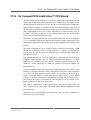
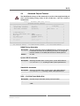
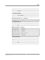
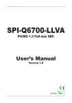
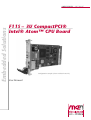
F11S – 3U CompactPCI®
Intel® Atom™ CPU Board
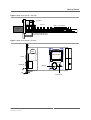
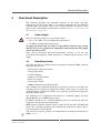
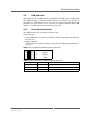
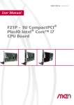
Configuration example (shown without heat sink)
User Manual
®
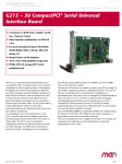
F11S - 3U CompactPCI® Intel® Atom™ CPU Board
F11S - 3U CompactPCI® Intel® Atom™ CPU Board
The F11S single-board computer is a versatile 3U Eurocard CompactPCI® board,
taking 8 HP or more front space depending on its configuration. It is equipped with
the Intel® Atom™ XL processor, an IA-32 core based on 45nm process technology.
Some processor versions are qualified for the extended temperature range. Due to
the low power architecture of the Intel® Atom™ processor, the CPU card has a total
power consumption of max. 5 to 7 Watts, while having a clock frequency of up to
1.6 GHz. A specially outlined heat sink efficiently takes away the heat from the
board, even in extended temperature range.
The F11S is designed especially for systems which require low power consumption,
e.g. as a computing platform for rugged industrial PCs in mobile applications or for
infotainment applications, offering the whole world of Windows® and Linux based
software.
The F11S accommodates up to 2 GB of directly soldered main memory, 2 MB
SRAM and an SPI boot flash. A SATA interface is available at CompactPCI®
connector J2. The storage capacity is completed by a CompactFlash® socket and a
microSD™ card slot.
One Gigabit Ethernet via one PCI Express® x1 link from the Intel® System
Controller Hub US15WP and one FPGA-controlled Fast Ethernet via RJ45
connectors are available at the front. Further standard front I/O interfaces are one
COM via a D-Sub connector, two USB 2.0, graphics (VGA up to UXGA) and
keyboard/mouse.
An on-board FPGA allows implementation of additional functionality such as serial
interfaces, CAN bus controllers, binary I/O, protocol converters, touch controllers
etc. to the needs of the individual application in a very flexible way. Before boot-up
of the system, the FPGA is loaded from the boot Flash. Updates of the FPGA
contents can be made inside the boot Flash during operation and are available after a
power-off of the system. A maximum of 3 SA-Adapters™ can be realized on one
F11S, with I/O accessible at the front panel.
The F11S is completed by a board management controller for temperature and
power supervision. It comes with a Phoenix® Award BIOS configurable for the
final application.
The F11S is screened or qualified for operation in a -40°C to +85°C conduction or
convection cooled environment.
MEN Mikro Elektronik GmbH
20F011S00 E3 – 2011-09-05
2
Technical Data
Technical Data
CPU
• Intel® Atom™ Z510P, Z530P, Z510PT or Z520PT
- Up to 1.6 GHz processor core frequency
- 400 MHz or 533 MHz system bus frequency
• Chipset
- Intel® system controller hub US15WP
Memory
• 512 KB L2 cache integrated in Atom processor
• Up to 2 GB DDR2 SDRAM system memory
- Soldered
- 400/533 MHz memory bus frequency locked to the FSB frequency
• 2 MB boot Flash
• 2 MB non-volatile SRAM, FPGA-controlled
• CompactFlash® card interface
- Via USB
- Type I
- DMA support
• One microSD™ card slot
- Via USB
- Compliant to SDIO Revision 1.1 and MMC Revision 4.0 (backward-compatible)
Mass Storage
• SATA
- Transfer rates up to 100MB/s
- Via PATA-to-SATA converter
- Accessible on rear I/O connector J2
Graphics
• Integrated in Intel® System Controller Hub US15WP
• Maximum resolution: 1600x1200 pixels
• VGA connector at front panel
- Via SDVO port from chipset
I/O
• USB
- Two Series A connectors at front panel
- One USB for PS/2 interface
- One USB for connection of CompactFlash®/microSD™
- UHCI and EHCI implementation
- Data rates up to 480 Mbits/s
MEN Mikro Elektronik GmbH
20F011S00 E3 – 2011-09-05
3
Technical Data
• Ethernet
- One 10/100/1000Base-T Ethernet channel
- Via one PCI Express® x1 linkfrom the chipset
- One 10/100Base-T Ethernet channel
- FPGA-controlled
- RJ45 connectors at front panel
- Two status LEDs for each channel
• One RS232 UART, FPGA-controlled
- D-Sub connector at front panel
- Via SA-Adapter™
- Data rates up to 115.2 kbits/s
- 60-byte transmit/receive buffer
- Handshake lines: CTS, RTS; DCD, DSR, DTR; RI
• 66 user I/O lines, FPGA-controlled
- Depending on FPGA configuration
- Accessible via rear I/O connector
• PS/2 keyboard/mouse
- PS/2 connector at front panel
- Via USB-PS/2 converter
Front Connections (Standard)
•
•
•
•
•
VGA
Two USB 2.0 (Series A)
Two Ethernet (RJ45)
One COM (D-Sub)
PS/2
FPGA
• Standard factory FPGA configuration:
- Main bus interface
- 16Z024_SRAM – SRAM controller
- 16Z125_UART – UART controller
- 16Z087_ETH – Ethernet controller
- 16Z034_GPIO – GPIO controller
• The FPGA offers the possibility to add customized I/O functionality. See FPGA.
PCI Express®
• One x1 link to connect local 1000Base-T Ethernet controller
• One x1 link for connection of PCI Express® to PCI bridge
• Data rate 250 MB/s (2.5 Gbits/s per lane)
MEN Mikro Elektronik GmbH
20F011S00 E3 – 2011-09-05
4
Technical Data
Miscellaneous
• Real-time clock buffered by a GoldCap or alternatively a battery (5 years life
cycle)
• Power supervision and watchdog
• Temperature measurement
• One status LED from board controller
• One FPGA status LED
• Six user LEDs (FPGA-controlled)
• Reset button
CompactPCI® Bus
•
•
•
•
Compliance with CompactPCI® Core Specification PICMG 2.0 R3.0
System slot
32-bit/33-MHz PCI Express®-to-PCI bridge
V(I/O): +3.3V
Electrical Specifications
• Supply voltage/power consumption:
- +5V (-3%/+5%), 0.9A typ. (with network connection)
- +3.3V (-3%/+5%), 0.9A typ. (with network connection)
- +12V (-5%/+5%), only provided for detection of 3.3V
Mechanical Specifications
• Dimensions: conforming to CompactPCI® specification for 3U boards
• Front panel: 8HP with ejector
• Weight: 458 g
Environmental Specifications
• Temperature range (operation):
- -40..+85°C (screened)
- Airflow: min. 1.0m/s
• Temperature range (storage): -40..+85°C
• Relative humidity (operation): max. 95% non-condensing
• Relative humidity (storage): max. 95% non-condensing
• Altitude: -300m to + 3,000m
• Shock: 15g/11ms
• Bump: 10g/16ms
• Vibration (sinusoidal): 1g/10..150Hz
• Conformal coating on request
MTBF
• 110,411h @ 40°C according to IEC/TR 62380 (RDF 2000)
Safety
• PCB manufactured with a flammability rating of 94V-0 by UL recognized manufacturers
MEN Mikro Elektronik GmbH
20F011S00 E3 – 2011-09-05
5
Technical Data
EMC
• Conforming to EN 55022 (radio disturbance), IEC 61000-4-2 (ESD) and IEC
61000-4-4 (burst)
BIOS
• Award BIOS
Software Support
•
•
•
•
•
Windows®
Linux
VxWorks® (on request)
QNX® (on request)
For more information on supported operating system versions and drivers see
online data sheet.
MEN Mikro Elektronik GmbH
20F011S00 E3 – 2011-09-05
6
Block Diagram
Block Diagram
F Front panel
Intel® Atom™
Processor
F
Compact Flash
and
MicroSD
USB 2.0
F
USB 2.0
B On‐board
Options
System Memory
DDR2 SDRAM
Intel® System Controller Hub
US15WP
SDVO to VGA
F
F
USB 2.0
F
USB 2.0 to PS/2
IDE (PATA)
PATA/SATA Converter
PCIe x1
PCIe x1
PCI Express to PCI Bridge
Ethernet
10/100/
1000BaseT PCI 32‐bit
LPC
F
Ethernet
10/100/
BaseT MII
UART
F
UART
F
UART
F
SRAM
FPGA
SPI Flash
F
CompactPCI Connectors
J1 and J2
7 LEDs
User I/O
MEN Mikro Elektronik GmbH
20F011S00 E3 – 2011-09-05
7
Configuration Options
Configuration Options
CPU
•
•
•
•
Intel® Atom™ Z530P, 1.6GHz, 533MHz FSB
Intel® Atom™ Z510P, 1.1GHz, 400MHz FSB
Intel® Atom™ Z520PT, 1.33GHz, 533MHz FSB
Intel® Atom™ Z510PT, 1.1GHz, 400MHz FSB
Memory
• CompactFlash®
- 0 MB up to maximum available
• MicroSD card
- 0 MB up to maximum available
• NAND Flash instead of CompactFlash®, microSD™ card and battery
- 0 MB up to maximum available
• mSATA slot instead of CompactFlash® and microSD™ card
- 0 MB up to maximum available
I/O
• USB
- One additional interface on M12 connector
• Ethernet
- Two interfaces on two 9-pin D-Sub connectors instead of two RJ45 connectors and COM interface
- Two interfaces on two M12 connectors instead of two RJ45 connectors and
COM interface
• UART
- Two additional UARTS on two SA-Adapters™ (12HP front)
Mechanical
• 4HP (without 2 Ethernet and UART)
• 8HP (standard)
• 12HP (with 2 additional UARTs)
Operating Temperature
• -40..+85°C qualified
Please note that some of these options may only be available for large volumes.
Please ask our sales staff for more information.
For available standard configurations see online data sheet.
MEN Mikro Elektronik GmbH
20F011S00 E3 – 2011-09-05
8
FPGA
FPGA
Flexible Configuration
• Customized I/O functions can be added to the FPGA.
• It depends on the board type, pin counts and number of logic elements which IP
cores make sense and/or can be implemented. Please contact MEN for information on feasibility.
• You can find more information on our web page "User I/O in FPGA"
FPGA Capabilities
• FPGA Altera® Cyclone® III EP3C16
- 119,088 logic elements
- 516,096 total RAM bits
• Connection
- Total available pin count: 66 pins
- Functions available via rear I/O connector J2
- SA-Adapters™ can be used to realize the physical lines.
MEN Mikro Elektronik GmbH
20F011S00 E3 – 2011-09-05
9
Product Safety
Product Safety
!
Lithium Battery
This board contains a lithium battery. There is a danger of explosion if the
battery is incorrectly replaced!
See Chapter 6 Maintenance on page 68.
!
Electrostatic Discharge (ESD)
Computer boards and components contain electrostatic sensitive devices.
Electrostatic discharge (ESD) can damage components. To protect the board and
other components against damage from static electricity, you should follow some
precautions whenever you work on your computer.
• Power down and unplug your computer system when working on the inside.
• Hold components by the edges and try not to touch the IC chips, leads, or circuitry.
• Use a grounded wrist strap before handling computer components.
• Place components on a grounded antistatic pad or on the bag that came with the
component whenever the components are separated from the system.
• Store the board only in its original ESD-protected packaging. Retain the original
packaging in case you need to return the board to MEN for repair.
MEN Mikro Elektronik GmbH
20F011S00 E3 – 2011-09-05
10
About this Document
About this Document
This user manual describes the hardware functions of the board, connection of
peripheral devices and integration into a system. It also provides additional
information for special applications and configurations of the board.
The manual does not include detailed information on individual components (data
sheets etc.). A list of literature is given in the appendix.
History
Issue
Comments
Date
E1
First issue
2010-03-17
E2
Completed and corrected front LED description,
Added mSATA option
Added note concerning SATA via CT12
Corrected J2 description
2010-11-04
E3
Modified chapters Chapter 2.4 Real-Time Clock on
page 24 and Chapter 2.1 Power Supply on page 23,
added Chapter 1.6.2 Installing Windows XP or Windows 7 via USB on page 22
2011-09-05
Conventions
!
italics
bold
monospace
This sign marks important notes or warnings concerning proper functionality of the
product described in this document. You should read them in any case.
Folder, file and function names are printed in italics.
Bold type is used for emphasis.
A monospaced font type is used for hexadecimal numbers, listings, C function
descriptions or wherever appropriate. Hexadecimal numbers are preceded by "0x".
comment
Comments embedded into coding examples are shown in green color.
hyperlink
Hyperlinks are printed in blue color.
The globe will show you where hyperlinks lead directly to the Internet, so you can
look for the latest information online.
IRQ#
/IRQ
Signal names followed by "#" or preceded by a slash ("/") indicate that this signal is
either active low or that it becomes active at a falling edge.
in/out
Signal directions in signal mnemonics tables generally refer to the corresponding
board or component, "in" meaning "to the board or component", "out" meaning
"coming from it".
Vertical lines on the outer margin signal technical changes to the previous issue of
the document.
MEN Mikro Elektronik GmbH
20F011S00 E3 – 2011-09-05
11
About this Document
Legal Information
MEN Mikro Elektronik GmbH ("MEN") reserves the right to make changes without further notice to any products herein.
MEN makes no warranty, representation or guarantee of any kind regarding the suitability of its products for any particular
purpose, nor does MEN assume any liability arising out of the application or use of any product or circuit, and specifically
disclaims any and all liability, including, without limitation, consequential or incidental damages. TO THE EXTENT
APPLICABLE, SPECIFICALLY EXCLUDED ARE ANY IMPLIED WARRANTIES ARISING BY OPERATION OF LAW,
CUSTOM OR USAGE, INCLUDING WITHOUT LIMITATION, THE IMPLIED WARRANTIES OF
MERCHANTABILITY AND FITNESS FOR A PARTICULAR PURPOSE OR USE. In no event shall MEN be liable for
more than the contract price for the products in question. If buyer does not notify servicer in writing within the foregoing
warranty period, servicer shall have no liability or obligation to buyer hereunder.
The manual is provided on the terms and understanding that:
1. MEN is not responsible for the results of any actions taken on the basis of information in the manual, nor for any error in or
omission from the manual; and
2. MEN is not engaged in rendering technical or other advice or services.
MEN expressly disclaims all and any liability and responsibility to any person, whether a reader of the manual or not, in
respect of anything, and of the consequences of anything, done or omitted to be done by any such person in reliance, whether
wholly or partially, on the whole or any part of the contents of the manual.
The correct function of MEN products in mission-critical and life-critical applications is limited to the environmental
specification given for each product in the technical user manual. The correct function of MEN products under extended
environmental conditions is limited to the individual requirement specification and subsequent validation documents for each
product for the applicable use case and has to be agreed upon in writing by MEN and the customer. Should the customer
purchase or use MEN products for any unintended or unauthorized application, the customer shall indemnify and hold MEN
and its officers, employees, subsidiaries, affiliates, and distributors harmless against all claims, costs, damages, and expenses,
and reasonable attorney fees arising out of, directly or indirectly, any claim or personal injury or death associated with such
unintended or unauthorized use, even if such claim alleges that MEN was negligent regarding the design or manufacture of the
part. In no case is MEN liable for the correct function of the technical installation where MEN products are a part of.
All products or services mentioned in this publication are identified by the trademarks, service marks, or product names as
designated by the companies who market those products. The trademarks and registered trademarks are held by the companies
producing them. Inquiries concerning such trademarks should be made directly to those companies.
Copyright © 2011 MEN Mikro Elektronik GmbH. All rights reserved.
Please recycle
Germany
MEN Mikro Elektronik GmbH
Neuwieder Straße 5-7
90411 Nuremberg
Phone +49-911-99 33 5-0
Fax +49-911-99 33 5-901
E-mail [email protected]
www.men.de
MEN Mikro Elektronik GmbH
20F011S00 E3 – 2011-09-05
France
MEN Mikro Elektronik SA
18, rue René Cassin
ZA de la Châtelaine
74240 Gaillard
Phone +33 (0) 450-955-312
Fax +33 (0) 450-955-211
E-mail [email protected]
www.men-france.fr
USA
MEN Micro, Inc.
24 North Main Street
Ambler, PA 19002
Phone (215) 542-9575
Fax (215) 542-9577
E-mail [email protected]
www.menmicro.com
12
Contents
Contents
1 Getting Started . . . . . . . . . . . . . . . . . . . . . . . . . . . . . . . . . . . . . . . . . . . . . . . .
1.1 Map of the Board. . . . . . . . . . . . . . . . . . . . . . . . . . . . . . . . . . . . . . . . .
1.2 Configuring the Hardware . . . . . . . . . . . . . . . . . . . . . . . . . . . . . . . . . .
1.3 Integrating the Board into a System . . . . . . . . . . . . . . . . . . . . . . . . . .
1.4 Troubleshooting at Start-up . . . . . . . . . . . . . . . . . . . . . . . . . . . . . . . . .
1.5 Configuring BIOS . . . . . . . . . . . . . . . . . . . . . . . . . . . . . . . . . . . . . . . .
1.6 Installing Operating System Software. . . . . . . . . . . . . . . . . . . . . . . . .
1.6.1
Installing Windows 2000 via USB . . . . . . . . . . . . . . . . . . . .
1.6.2
Installing Windows XP or Windows 7 via USB . . . . . . . . . .
1.7 Installing Driver Software . . . . . . . . . . . . . . . . . . . . . . . . . . . . . . . . . .
17
17
20
21
22
22
22
22
22
22
2 Functional Description . . . . . . . . . . . . . . . . . . . . . . . . . . . . . . . . . . . . . . . . . .
2.1 Power Supply. . . . . . . . . . . . . . . . . . . . . . . . . . . . . . . . . . . . . . . . . . . .
2.2 Board Supervision . . . . . . . . . . . . . . . . . . . . . . . . . . . . . . . . . . . . . . . .
2.3 Reset . . . . . . . . . . . . . . . . . . . . . . . . . . . . . . . . . . . . . . . . . . . . . . . . . .
2.4 Real-Time Clock . . . . . . . . . . . . . . . . . . . . . . . . . . . . . . . . . . . . . . . . .
2.5 Processor Core. . . . . . . . . . . . . . . . . . . . . . . . . . . . . . . . . . . . . . . . . . .
2.5.1
Thermal Considerations . . . . . . . . . . . . . . . . . . . . . . . . . . . .
2.6 Memory . . . . . . . . . . . . . . . . . . . . . . . . . . . . . . . . . . . . . . . . . . . . . . . .
2.6.1
DRAM System Memory . . . . . . . . . . . . . . . . . . . . . . . . . . . .
2.6.2
Boot Flash . . . . . . . . . . . . . . . . . . . . . . . . . . . . . . . . . . . . . . .
2.6.3
EEPROM. . . . . . . . . . . . . . . . . . . . . . . . . . . . . . . . . . . . . . . .
2.6.4
SRAM . . . . . . . . . . . . . . . . . . . . . . . . . . . . . . . . . . . . . . . . . .
2.7 Mass Storage . . . . . . . . . . . . . . . . . . . . . . . . . . . . . . . . . . . . . . . . . . . .
2.7.1
CompactFlash and microSD Card. . . . . . . . . . . . . . . . . . . . .
2.7.2
Mass Storage Options . . . . . . . . . . . . . . . . . . . . . . . . . . . . . .
2.7.3
Serial ATA (SATA) . . . . . . . . . . . . . . . . . . . . . . . . . . . . . . . .
2.8 Graphics. . . . . . . . . . . . . . . . . . . . . . . . . . . . . . . . . . . . . . . . . . . . . . . .
2.8.1
Connection via VGA. . . . . . . . . . . . . . . . . . . . . . . . . . . . . . .
2.9 USB Interfaces. . . . . . . . . . . . . . . . . . . . . . . . . . . . . . . . . . . . . . . . . . .
2.9.1
Front-Panel Connection . . . . . . . . . . . . . . . . . . . . . . . . . . . .
2.10 Ethernet Interfaces. . . . . . . . . . . . . . . . . . . . . . . . . . . . . . . . . . . . . . . .
2.10.1 Connector Options . . . . . . . . . . . . . . . . . . . . . . . . . . . . . . . .
2.10.2 Ethernet Status LEDs . . . . . . . . . . . . . . . . . . . . . . . . . . . . . .
2.11 UART Interfaces . . . . . . . . . . . . . . . . . . . . . . . . . . . . . . . . . . . . . . . . .
2.11.1 UART Interface Options . . . . . . . . . . . . . . . . . . . . . . . . . . . .
2.12 User I/O . . . . . . . . . . . . . . . . . . . . . . . . . . . . . . . . . . . . . . . . . . . . . . . .
2.13 PS/2 Keyboard/Mouse . . . . . . . . . . . . . . . . . . . . . . . . . . . . . . . . . . . . .
2.13.1 Reset Button . . . . . . . . . . . . . . . . . . . . . . . . . . . . . . . . . . . . .
2.14 Front Panel LEDs . . . . . . . . . . . . . . . . . . . . . . . . . . . . . . . . . . . . . . . .
2.14.1 Status LED . . . . . . . . . . . . . . . . . . . . . . . . . . . . . . . . . . . . . .
2.14.2 User-definable LEDs. . . . . . . . . . . . . . . . . . . . . . . . . . . . . . .
23
23
23
24
24
24
24
25
25
25
25
25
26
26
26
27
27
27
28
28
29
30
32
33
34
35
35
35
36
36
37
MEN Mikro Elektronik GmbH
20F011S00 E3 – 2011-09-05
13
Contents
2.15 CompactPCI Interface . . . . . . . . . . . . . . . . . . . . . . . . . . . . . . . . . . . . . 38
2.15.1 General . . . . . . . . . . . . . . . . . . . . . . . . . . . . . . . . . . . . . . . . . 38
2.15.2 CompactPCI Extensions and Rear I/O . . . . . . . . . . . . . . . . . 38
3 FPGA . . . . . . . . . . . . . . . . . . . . . . . . . . . . . . . . . . . . . . . . . . . . . . . . . . . . . . . .
3.1 General . . . . . . . . . . . . . . . . . . . . . . . . . . . . . . . . . . . . . . . . . . . . . . . .
3.2 Standard Factory FPGA Configuration . . . . . . . . . . . . . . . . . . . . . . . .
3.2.1
Configuration Table. . . . . . . . . . . . . . . . . . . . . . . . . . . . . . . .
3.3 Software Support . . . . . . . . . . . . . . . . . . . . . . . . . . . . . . . . . . . . . . . . .
3.4 Possible Front and Rear I/O Extensions . . . . . . . . . . . . . . . . . . . . . . .
41
41
41
42
43
43
4 BIOS . . . . . . . . . . . . . . . . . . . . . . . . . . . . . . . . . . . . . . . . . . . . . . . . . . . . . . . . .
4.1 Main Menu . . . . . . . . . . . . . . . . . . . . . . . . . . . . . . . . . . . . . . . . . . . . .
4.2 Standard CMOS Features . . . . . . . . . . . . . . . . . . . . . . . . . . . . . . . . . .
4.3 Advanced BIOS Features . . . . . . . . . . . . . . . . . . . . . . . . . . . . . . . . . .
4.4 Advanced Chipset Features . . . . . . . . . . . . . . . . . . . . . . . . . . . . . . . . .
4.5 Integrated Peripherals . . . . . . . . . . . . . . . . . . . . . . . . . . . . . . . . . . . . .
4.6 Power Management Setup . . . . . . . . . . . . . . . . . . . . . . . . . . . . . . . . . .
4.7 PNP/PCI Configurations . . . . . . . . . . . . . . . . . . . . . . . . . . . . . . . . . . .
4.8 PC Health Status . . . . . . . . . . . . . . . . . . . . . . . . . . . . . . . . . . . . . . . . .
4.9 Frequency/Voltage Control . . . . . . . . . . . . . . . . . . . . . . . . . . . . . . . . .
4.10 Load Fail-Safe Defaults. . . . . . . . . . . . . . . . . . . . . . . . . . . . . . . . . . . .
4.11 Load Optimized Defaults. . . . . . . . . . . . . . . . . . . . . . . . . . . . . . . . . . .
4.12 Set Password . . . . . . . . . . . . . . . . . . . . . . . . . . . . . . . . . . . . . . . . . . . .
4.13 Save & Exit Setup . . . . . . . . . . . . . . . . . . . . . . . . . . . . . . . . . . . . . . . .
4.14 Exit without Saving . . . . . . . . . . . . . . . . . . . . . . . . . . . . . . . . . . . . . . .
44
44
45
47
52
54
58
60
62
62
63
63
63
63
63
5 Organization of the Board . . . . . . . . . . . . . . . . . . . . . . . . . . . . . . . . . . . . . . .
5.1 Memory Mappings . . . . . . . . . . . . . . . . . . . . . . . . . . . . . . . . . . . . . . .
5.1.1
Processor View of the Memory Map. . . . . . . . . . . . . . . . . . .
5.1.2
I/O Memory Map . . . . . . . . . . . . . . . . . . . . . . . . . . . . . . . . .
5.2 PCI Devices . . . . . . . . . . . . . . . . . . . . . . . . . . . . . . . . . . . . . . . . . . . . .
5.3 SMBus Devices . . . . . . . . . . . . . . . . . . . . . . . . . . . . . . . . . . . . . . . . . .
5.4 Interrupt Mapping . . . . . . . . . . . . . . . . . . . . . . . . . . . . . . . . . . . . . . . .
64
64
64
65
66
67
67
6 Maintenance . . . . . . . . . . . . . . . . . . . . . . . . . . . . . . . . . . . . . . . . . . . . . . . . . . 68
6.1 Lithium Battery . . . . . . . . . . . . . . . . . . . . . . . . . . . . . . . . . . . . . . . . . . 68
7 Appendix . . . . . . . . . . . . . . . . . . . . . . . . . . . . . . . . . . . . . . . . . . . . . . . . . . . . .
7.1 Literature and Web Resources . . . . . . . . . . . . . . . . . . . . . . . . . . . . . . .
7.1.1
SATA . . . . . . . . . . . . . . . . . . . . . . . . . . . . . . . . . . . . . . . . . . .
7.1.2
USB . . . . . . . . . . . . . . . . . . . . . . . . . . . . . . . . . . . . . . . . . . . .
7.1.3
Ethernet . . . . . . . . . . . . . . . . . . . . . . . . . . . . . . . . . . . . . . . . .
7.1.4
PCI Express. . . . . . . . . . . . . . . . . . . . . . . . . . . . . . . . . . . . . .
7.1.5
CompactPCI/PCI. . . . . . . . . . . . . . . . . . . . . . . . . . . . . . . . . .
7.2 Finding out the Product’s Article Number, Revision and
Serial Number . . . . . . . . . . . . . . . . . . . . . . . . . . . . . . . . . . . . . . . . . . .
MEN Mikro Elektronik GmbH
20F011S00 E3 – 2011-09-05
69
69
69
69
69
69
70
70
14
Figures
Figure 1.
Figure 2.
Figure 3.
Figure 4.
Figure 5.
Figure 6.
Figure 7.
MEN Mikro Elektronik GmbH
20F011S00 E3 – 2011-09-05
Map of the board – front panel . . . . . . . . . . . . . . . . . . . . . . . . . . . . . . .
Map of the board – side view . . . . . . . . . . . . . . . . . . . . . . . . . . . . . . . .
Map of the board – top view. . . . . . . . . . . . . . . . . . . . . . . . . . . . . . . . .
Map of the board – bottom view . . . . . . . . . . . . . . . . . . . . . . . . . . . . .
FPGA – Block diagram . . . . . . . . . . . . . . . . . . . . . . . . . . . . . . . . . . . .
Position of battery on the CompactFlash adapter on the F11S. . . . . . .
Labels giving the product’s article number, revision and
serial number . . . . . . . . . . . . . . . . . . . . . . . . . . . . . . . . . . . . . . . . . . . .
17
18
18
19
42
68
70
15
Tables
Table 1.
Table 2.
Table 3.
Table 4.
Table 5.
Table 6.
Table 7.
Table 8.
Table 9.
Table 10.
Table 11.
Table 12.
Table 13.
Table 14.
Table 15.
Table 16.
Table 17.
Table 18.
Table 19.
Table 20.
Table 21.
Table 22.
Table 23.
Table 24.
Table 25.
Table 26.
Table 27.
MEN Mikro Elektronik GmbH
20F011S00 E3 – 2011-09-05
Retention times of Goldcap and battery . . . . . . . . . . . . . . . . . . . . . . . .
Processor core options on F11S . . . . . . . . . . . . . . . . . . . . . . . . . . . . . .
Pin assignment of 15-pin HD-Sub VGA receptacle connector . . . . . .
Signal mnemonics of 15-pin HD-Sub VGA connector . . . . . . . . . . . .
Pin assignment of USB front-panel connectors . . . . . . . . . . . . . . . . . .
Signal mnemonics of USB front-panel connectors . . . . . . . . . . . . . . .
Signal mnemonics of Ethernet front-panel connectors. . . . . . . . . . . . .
Pin assignment of 8-pin RJ45 Ethernet 10/100/1000Base-T
connectors (LAN1/LAN2) . . . . . . . . . . . . . . . . . . . . . . . . . . . . . . . . . .
Pin assignment of 9-pin D-Sub 1000Base-T plug connector (LAN2) .
Pin assignment of 9-pin D-Sub 100Base-T plug connector (LAN1) . .
Pin assignment of 8-pin M12 1000Base-T plug connector (LAN2) . .
Pin assignment of 8-pin M12 100Base-T plug connector (LAN1) . . .
Ethernet status LEDs . . . . . . . . . . . . . . . . . . . . . . . . . . . . . . . . . . . . . .
Pin assignment of 9-pin D-Sub connector for RS232 . . . . . . . . . . . . .
Signal Mnemonics for the RS232 COM Interfaces . . . . . . . . . . . . . . .
Pin assignment of the 6-pin Mini DIN PS/2 connector . . . . . . . . . . . .
Signal mnemonics of PS/2 Interface . . . . . . . . . . . . . . . . . . . . . . . . . .
Front panel LEDs on the F11S . . . . . . . . . . . . . . . . . . . . . . . . . . . . . . .
Error codes signaled by board management controller via
LED flashes . . . . . . . . . . . . . . . . . . . . . . . . . . . . . . . . . . . . . . . . . . . . .
Pin Assignment of CompactPCI Connector J2 (110-pin type "B"
modified) . . . . . . . . . . . . . . . . . . . . . . . . . . . . . . . . . . . . . . . . . . . . . . .
Signal mnemonics of CompactPCI connector J2 – CompactPCI and
rear I/O extension . . . . . . . . . . . . . . . . . . . . . . . . . . . . . . . . . . . . . . . . .
FPGA – Factory standard configuration table for F11S. . . . . . . . . . . .
Memory map – processor view . . . . . . . . . . . . . . . . . . . . . . . . . . . . . .
Memory map - I/O . . . . . . . . . . . . . . . . . . . . . . . . . . . . . . . . . . . . . . . .
PCI Devices . . . . . . . . . . . . . . . . . . . . . . . . . . . . . . . . . . . . . . . . . . . . .
SMBus devices . . . . . . . . . . . . . . . . . . . . . . . . . . . . . . . . . . . . . . . . . . .
Interrupts. . . . . . . . . . . . . . . . . . . . . . . . . . . . . . . . . . . . . . . . . . . . . . . .
24
24
27
27
28
28
29
30
30
31
31
31
32
33
33
35
35
36
37
39
40
42
64
65
66
67
67
16
Getting Started
1
Getting Started
This chapter gives an overview of the board and some hints for first installation in a
system.
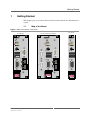
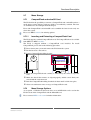
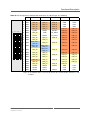
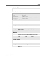
1.1
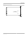
Map of the Board
Figure 1. Map of the board – front panel
F11S Standard
F11S with 2 additional SA-Adapters
®
F11S with 4HP
®
®
1 2 3 4
1 2 3 4
1 2 3 4
RST
5 6 7 8
RST
5 6 7 8
RST
5 6 7 8
KB/MS
KB/MS
USB1
KB/MS
USB1
X1
USB1
X1
X2
USB2
USB2
LAN
1
VGA
VGA
A
L
A
L
MEN Mikro Elektronik GmbH
20F011S00 E3 – 2011-09-05
VGA
A
L
X3
A
L
LAN
2
F11S
USB2
LAN
1
LAN
2
F11S
F11S
17
Getting Started
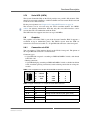
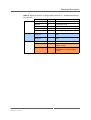
Figure 2. Map of the board – side view
SA-Adapter
Plug-on Board
Heat sink
Battery
CompactFlash
Plug-on Board
Handle
Main Board
2 optional SA-Adapters (board
version with 12 HP front panel)
Figure 3. Map of the board – top view
Gold
Cap
CompactFlash
COM
met.
met.
Ethernet
Battery
microSD™
MEN Mikro Elektronik GmbH
20F011S00 E3 – 2011-09-05
18
Getting Started
Figure 4. Map of the board – bottom view
met.
met.
SA-Adapter
Connectors (optional)
MEN Mikro Elektronik GmbH
20F011S00 E3 – 2011-09-05
19
Getting Started
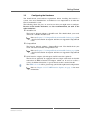
1.2
Configuring the Hardware
You should check your hardware requirements before installing the board in a
system, since most modifications are difficult or even impossible to do when the
board is mounted in a rack.
The following check list gives an overview on what you might want to configure.
Because of the board’s mechanics, we also recommend that you stick to the
order of this list!
microSD card
The board is shipped without a microSD card. You should check your needs
and install a suitable microSD card.
Refer to Chapter 2.7.1 CompactFlash and microSD Card on page 26 for
a detailed installation description and hints on supported CompactFlash
cards.
CompactFlash
The board is shipped without a CompactFlash card. You should check your
needs and install a suitable CompactFlash card.
Refer to Chapter 2.7.1 CompactFlash and microSD Card on page 26 for
a detailed installation description and hints on supported CompactFlash
cards.
Serial interface adapters (SA-Adapters) for I/O extension (optional)
The board can optionally be equipped with two 10-pin connectors for flexible
connection of MEN standard SA-Adapters which can be used to realize a
variety of additional functions. A special board version is needed for this.
The MEN sales staff will be glad to help you find the right board configuration.
Refer to Chapter 2.11.1 UART Interface Options on page 34 for more
information.
MEN Mikro Elektronik GmbH
20F011S00 E3 – 2011-09-05
20
Getting Started
1.3
Integrating the Board into a System
You can use the following check list when installing the F11S in a system for the
first time and with minimum configuration.
!
The board is completely trimmed on delivery.
Power-down the system.
Remove all boards from the CompactPCI system.
Insert the F11S into the system slot of your CompactPCI system, making sure
that the CompactPCI connectors are properly aligned.
Note: The system slot of every CompactPCI system is marked by a
triangle
on the backplane and/or at the front panel. It also has red guide rails.
If you want to use a terminal via RS232:
Connect a terminal to the standard RS232 interface (D-Sub connector).
Set your terminal to the following protocol:
-
9600 or 19200 or 115200 baud data transmission rate
8 data bits
1 stop bit
No parity
If you don’t want to use a terminal via RS232:
Connect a PS/2 keyboard and mouse to the PS/2 connector at the front panel.
Or: Connect a USB keyboard and mouse to the USB connectors at the front
panel.
Connect a CRT or flat-panel display to the VGA connector at the front panel.
Power-up the system.
You can fork up the BIOS setup menu by hitting the <DEL> key (see Chapter 4
BIOS on page 44).
Now you can make configurations in BIOS (see Chapter 4 BIOS on page 44).
Observe the installation instructions for the respective software.
MEN Mikro Elektronik GmbH
20F011S00 E3 – 2011-09-05
21
Getting Started
1.4
Troubleshooting at Start-up
If you have any problems at start-up of the F11S, you can start the board with BIOS
default settings for troubleshooting. Please refer to Chapter 4 BIOS on page 44.
1.5
Configuring BIOS
The F11S is equipped with an industry-standard BIOS. Normally you won’t need to
make any changes in the BIOS setup. If you do, however, you find further details on
the F11S’s BIOS in Chapter 4 BIOS on page 44.
1.6
Installing Operating System Software
The board supports Windows®, Linux, VxWorks® (on request), QNX® (on
request).
!
By default, no operating system is installed on the board. Please refer to the
respective manufacturer's documentation on how to install operating system
software!
You can find any software available on MEN’s website.
1.6.1
Installing Windows 2000 via USB
If you want to install Windows 2000 using a USB CD-ROM drive, you must install
from a Windows 2000 CD including Service Pack 4 to avoid problems. This is a
known Windows problem.
1.6.2
Installing Windows XP or Windows 7 via USB
The microSD card and the CompactFlash of the F11S are connected via USB. A
standard Windows operating system (like Windows XP Professional or Windows 7
Ultimate) does not support direct installation on USB memory devices.
There are three possible solutions:
• The F11S offers the possibility to assemble an mSATA slot instead of the CompactFlash and the microSD. See Chapter 2.7.2 Mass Storage Options on page 26.
• Add a hard drive (SATA, mSATA) on a peripheral board or side card
• Switch to an Embedded Windows (like Windows Embedded Standard or Windows Embedded Standard 7). These Embedded Windows operating systems support being installed on and booted from a USB device.
Linux supports booting from a USB device without problems.
1.7
Installing Driver Software
For a detailed description on how to install driver software please refer to the
respective documentation.
You can find any driver software available for download on MEN’s website.
MEN Mikro Elektronik GmbH
20F011S00 E3 – 2011-09-05
22
Functional Description
2
Functional Description
The following describes the individual functions of the board and their
configuration on the board. There is no detailed description of the individual
controller chips and the CPU. They can be obtained from the data sheets or data
books of the semiconductor manufacturer concerned (Chapter 7.1 Literature and
Web Resources on page 69).
2.1
!
Power Supply
There are only two possible ways to power the F11S:
• +5V, +3.3V and +12V via CompactPCI connector J1
• +5V only via CompactPCI connector J1
To supply the board with 3.3V and 5V is not allowed and may cause serious
damage. If +3.3V are supplied via CompactPCI connector J1, the +12V supply
always has to be present.
If the +12V are not present, the board automatically generates +3.3V and also
feeds them to the backplane, which would cause a conflict with the external +3.3V
supply.
2.2
Board Supervision
The F11S provides an intelligent board management controller (BMC) with the
following main features:
•
•
•
•
•
•
•
Board power sequencing control
Voltage supervision
System watchdog
Software reset functionality
Error state logging
Power mode settings
SMBus communication with main CPU
The watchdog device monitors the board on operating system level. If enabled, the
watchdog must be triggered by application software. If the trigger is overdue, the
watchdog initiates a board reset and this way can put the system back into operation
when the software hangs.
The watchdog uses a configurable time interval or is disabled. Settings are made
through BIOS or via an MEN software driver.
In addition, the F11S uses a National LM95245 device to measure the CPU die
temperature and the local board temperature.
MEN provides dedicated software drivers for the board controller and LM95245
device. For a detailed description of the functionality of the driver software please
refer to the drivers’ documentation.
You can find any driver software and documentation available for download on
MEN’s website.
MEN Mikro Elektronik GmbH
20F011S00 E3 – 2011-09-05
23
Functional Description
2.3
Reset
The F11S generates its own reset signal. You can wake it up from reset state by
externally switching the power supply off and on.
2.4
Real-Time Clock
For data retention during power off the RTC is backed up by a GoldCap capacitor
and - for retention of time/date data after a power off of more than 8-10 hours - also
by a battery.
Under normal conditions, replacement should be superfluous during lifetime of the
board. The RTC can generate interrupt requests to the chipset.
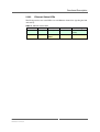
The retention time depends on whether there is an SRAM on the board. For the
different retention times see Table 1, Retention times of Goldcap and battery.
Table 1. Retention times of Goldcap and battery
SRAM+RTC
Only RTC, without SRAM
With Goldcap
16.5 h
33 h
With Battery
4 years
8 years
2.5
Processor Core
The F11S is equipped with an Intel Atom Z530 (1.6 GHz) or a Z510 (1.1 GHz)
processor. The following table gives a performance overview:
Table 2. Processor core options on F11S
Processor Type
Core Frequency
L2 Cache
Front Side Bus
Atom Z510P
1.1 GHz
512 KB
400 MHz
Atom Z530P
1.6 GHz
512 KB
533 MHz
Atom Z510PT
1.1GHz
512 KB
400MHz
Atom Z520PT
1.33GHz
512 KB
533MHz
2.5.1
Thermal Considerations
A suitable heat sink is provided to meet thermal requirements.
!
Please note that if you use any other heat sink than that supplied by MEN, or no heat
sink at all, warranty on functionality and reliability of the F11S may cease. If you
have any questions or problems regarding thermal behavior, please contact MEN.
MEN Mikro Elektronik GmbH
20F011S00 E3 – 2011-09-05
24
Functional Description
2.6
Memory
The standard board versions provide a memory configuration suitable for many
applications. However, memory on the F11S can also be configured for your needs.
For standard memory sizes and ordering options please see MEN’s website.
2.6.1
DRAM System Memory
The board provides up to 2 GB on-board, soldered DDR2 (double data rate)
SDRAM. The memory bus is 64 bits wide (one channel) and operates with up to
533 MHz.
The F11S supports memory down technology. The memory is not realized with
complete modules. Instead single memory chips with a maximum of 2 Gbit per chip
are used.
2.6.2
Boot Flash
The F11S has a SPI boot Flash device. The system controller hub (SCH) is
connected to the FPGA via the LPC bus. The SPI Flash is connected to the FPGA.
The flash device is used to store the system BIOS and FPGA configuration. The
LPC bus to SPI conversion is implemented in an IP core in the FPGA.
2.6.3
EEPROM
The board has a 2-kbit serial EEPROM for factory data.
2.6.4
SRAM
The F11S supports a 2 MB SRAM which is buffered by a Goldcap or the battery. It
is controlled by an IP core in the FPGA.
MEN Mikro Elektronik GmbH
20F011S00 E3 – 2011-09-05
25
Functional Description
2.7
Mass Storage
2.7.1
CompactFlash and microSD Card
The F11S offers the possibility to connect a CompactFlash and a microSD card on a
small adapter card in the heat sink area which is assembled by standard. The slots
are controlled via one USB port from the chipset.
Even with CompactFlash and microSD card assembled the board needs only one
slot in the system.
Please see MEN’s website for ordering options.
2.7.1.1
Inserting and Extracting a CompactFlash Card
The F11S supports standard CompactFlash cards. For CompactFlash cards available
from MEN see MEN’s website.
The F11S is shipped without a CompactFlash card installed. To install
CompactFlash, please stick to the following procedure.
Power down your system and remove the F11S from the system.
Put the board on a flat surface.
Lift the CompactFlash holding bracket.
Gold
Cap
CompactFlash
met.
met.
Insert the CompactFlash card carefully as indicated by the arrow on top of the
card.
Make sure that all the contacts are aligned properly and the card is firmly connected with the card connector.
Push the CompactFlash holding bracket back down until it clicks into place.
Observe manufacturer notes on usage of CompactFlash cards.
2.7.2
Mass Storage Options
As an option, a USB based solid state drive or an mSATA disk can be used on the
F11S instead of the CompactFlash and the MicroSD card.
Please contact MEN’s sales team for further information.
MEN Mikro Elektronik GmbH
20F011S00 E3 – 2011-09-05
26
Functional Description
2.7.3
Serial ATA (SATA)
The System Controller Hub of the F11S provides one parallel ATA channel. This
channel is converted to SATA by a PATA-to-SATA converter on the F11S board and
led to the J2 rear I/O connector.
For the pin assignment see Chapter 2.15 CompactPCI Interface on page 38.
The interface can be accessed using the CT12 transition module. See MEN’s
website for ordering information. Note that only this one SATA interface can be
used on the CT12 in combination with the F11S.
The SATA interface supports transfer rates up to 100 MB/s.
2.8
Graphics
The graphics core of the F11S is part of the System Controller Hub. It supports a
resolution of up to 1600x1200 pixels. The SDVO signals from the SCH are
converted to VGA and accessible at a 15-pin HD-Sub connector at the front panel.
2.8.1
Connection via VGA
You can connect a VGA monitor directly at the F11S’s front panel. The pinout of
the 15-pin HD-Sub connector is standard VGA.
Connector types:
• 15-pin HD-Sub receptacle according to DIN41652/MIL-C-24308, with thread
bolt UNC 4-40
• Mating connector:
15-pin HD-Sub plug according to DIN41652/MIL-C-24308, available for ribbon
cable (insulation piercing connection), hand-soldering connection or crimp connection
Table 3. Pin assignment of 15-pin HD-Sub VGA receptacle connector
10
15
5
11
1
6
15
SCL
10
GND
5
GND
14
VSYNC
9
-
4
-
13
HSYNC
8
GND
3
B
12
SDA
7
GND
2
G
11
-
6
GND
1
R
Table 4. Signal mnemonics of 15-pin HD-Sub VGA connector
Signal
Function
GND
-
Ground
HSYNC
out
Horizontal synchronization
R, G, B
out
Analog monitor interface (red, green, blue)
SCL
out
Monitor I²C interface
SDA
in/out
VSYNC
out
MEN Mikro Elektronik GmbH
20F011S00 E3 – 2011-09-05
Direction
Vertical synchronization
27
Functional Description
2.9
USB Interfaces
The F11S provides six USB interfaces controlled by the SCH system controller hub.
Two USB interfaces are routed to standard front-panel connectors, one interface is
connected to a USB-PS/2 converter, one is used to control the CompactFlash and
microSD card, one interface can be used for an optional additional front USB
interface on an M12 connector, the sixth one is not used.
2.9.1
Front-Panel Connection
Two USB interfaces are accessible at the front panel.
Connector types:
• 4-pin USB Series A receptacle according to Universal Serial Bus Specification
Revision 1.0
• Mating connector:
4-pin USB Series A plug according to Universal Serial Bus Specification Revision 1.0
Table 5. Pin assignment of USB front-panel connectors
1
2
3
4
1
+5V
2
USB_D-
3
USB_D+
4
GND
Table 6. Signal mnemonics of USB front-panel connectors
Signal
Direction
+5V
out
+5 V power supply
GND
-
Digital ground
USB_D+, USB_D- in/out
MEN Mikro Elektronik GmbH
20F011S00 E3 – 2011-09-05
Function
USB lines, differential pair
28
Functional Description
2.10
Ethernet Interfaces
The F11S provides two Ethernet channels on two RJ45 connectors at the front
panel. One is a Gigabit Ethernet interface which is controlled by the chipset via a
PCI Express x1 link. The other interface is a Fast Ethernet and is controlled via an
IP core in the FPGA.
!
The unique MAC address is set at the factory and should not be changed. Any
attempt to change this address may create node or bus contention and thereby render
the board inoperable. The MAC addresses on F11S are:
• LAN1 (Fast) : 0x 00 C0 3A 9E Cx xx - 0x 00 C0 3A 9E FF FF
• LAN2 (Gigabit) : 0x 00 C0 3A 9E 8x xx - 0x 00 C0 3A 9E BF FF
where "00 C0 3A" is the MEN vendor code, "9E" is the MEN product code. The last
four digits depend on the interface and the serial number of the product. The serial
number is added to the offset, for example for LAN1:
• Serial number 0042: 0x xx xx = 0x8000 + 0x002A = 0x 80 2A.
(See Chapter 7.2 Finding out the Product’s Article Number, Revision and Serial
Number on page 70.)
Connector types:
• Modular 8/8-pin mounting jack according to FCC68
• Mating connector:
Modular 8/8-pin plug according to FCC68
Table 7. Signal mnemonics of Ethernet front-panel connectors
Signal
Function
BI_Dx+/-
in/out
Differential pairs of data lines for 1000Base-T
RX+/-
in
Differential pair of receive data lines for 10/
100Base-T
TX+/-
out
Differential pair of transmit data lines for 10/
100Base-T
MEN Mikro Elektronik GmbH
20F011S00 E3 – 2011-09-05
Direction
29
Functional Description
Connection via RJ45 Connectors
Table 8. Pin assignment of 8-pin RJ45 Ethernet 10/100/1000Base-T connectors
(LAN1/LAN2)
1
8
2.10.1
1000Base-T
(LAN2)
10/100Base-T
(LAN1)
1
BI_DA+
TX+
2
BI_DA-
TX-
3
BI_DB+
RX+
4
BI_DC+
-
5
BI_DC-
-
6
BI_DB-
RX-
7
BI_DD+
-
8
BI_DD-
-
Connector Options
The F11S offers the possibility to route the two Ethernet interfaces either to two 9pin D-Sub connectors or two M12 connectors. In both configurations the RS232
UART interface is replaced by one Ethernet connector.
Please contact MEN’s sales team for further information about possible configurations and special board versions.
Connection via 9-pin D-Sub Connectors
Connector types:
• 9-pin D-Sub plug according to DIN41652/MIL-C-24308, with thread bolt UNC
4-40
• Mating connector:
9-pin D-Sub receptacle according to DIN41652/MIL-C-24308, available for ribbon cable (insulation piercing connection), hand-soldering connection or crimp
connection
Table 9. Pin assignment of 9-pin D-Sub 1000Base-T plug connector (LAN2)
6
9
MEN Mikro Elektronik GmbH
20F011S00 E3 – 2011-09-05
1
5
1
BI_DA+
6
BI_DA-
2
BI_DC+
7
BI_DC-
3
-
8
BI_DD-
4
BI_DD+
9
BI_DB-
5
BI_DB+
30
Functional Description
Table 10. Pin assignment of 9-pin D-Sub 100Base-T plug connector (LAN1)
1
6
9
5
1
TX1+
6
TX1-
2
-
7
-
3
-
8
-
4
-
9
RX1-
5
RX1+
Connection via M12 Connectors
Connector types:
• 8-pin M12 SPEEDCON socket, A-coded, rear/screw mounting with M12 thread,
e.g. Phoenix Contact SACC-DSIV-FS-8CON-L90 SCO
• Mating connector: 8-pin M12 connector
Table 11. Pin assignment of 8-pin M12 1000Base-T plug connector (LAN2)
7
8
1
2
1
BI_DC-
2
BI_DD+
3
BI_DD-
4
BI_DA-
5
BI_DB+
6
BI_DA+
7
BI_DC+
8
BI_DB-
6
3
5
4
Table 12. Pin assignment of 8-pin M12 100Base-T plug connector (LAN1)
7
8
1
2
1
-
2
-
3
-
4
TX1-
5
RX1+
6
TX1+
7
-
8
RX1-
6
5
MEN Mikro Elektronik GmbH
20F011S00 E3 – 2011-09-05
3
4
31
Functional Description
2.10.2
Ethernet Status LEDs
The F11S provides two status LEDs for each Ethernet channel for signaling the link
and activity:
Table 13. Ethernet status LEDs
LED color
On
Off
Blinking
Green
Activity LED
Link Up
No Link
Transmit/Receive
Activity
Yellow
Speed LED
Link 100
Mbit/s
Link 10 Mbit/s
n/ a
MEN Mikro Elektronik GmbH
20F011S00 E3 – 2011-09-05
Mode
32
Functional Description
2.11
UART Interfaces
The standard F11S provides one RS232 interface at the front panel via a 9-pin DSub connector. The interface is controlled by an IP core in the onboard FPGA.
For more information on the general structure of the FPGA, please see Chapter 3
FPGA on page 41.
Connector types
• 9-pin D-Sub plug according to DIN41652/MIL-C-24308, with thread bolt
UNC4-40
• Mating connector:
9-pin D-Sub receptacle according to DIN41652/MIL-C-24308, available for ribbon cable (insulation piercing connection), hand-soldering connection or crimp
connection
Table 14. Pin assignment of 9-pin D-Sub connector for RS232
6
9
1
5
1
DCD#
6
DSR#
2
RXD
7
RTS#
3
TXD
8
CTS#
4
DTR#
9
RI#
5
GND
Table 15. Signal Mnemonics for the RS232 COM Interfaces
Signal
Function
CTS#
in
Clear to send
DCD#
in
Data carrier detect
DSR#
in
Data set ready
DTR#
out
Data terminal ready
GND
-
Ground
RTS#
out
Request to send
RXD
in
Receive data
TXD
out
Transmit data
MEN Mikro Elektronik GmbH
20F011S00 E3 – 2011-09-05
Direction
33
Functional Description
2.11.1
UART Interface Options
As an option, the board offers the possibility to assemble two additional connectors
at the bottom side of the board for direct connection of two MEN standard SAAdapters. This way, two additional UART interfaces can be used which can be
flexibly configured as RS232, RS422/485 or TTY, as needed. A special board
version with a 12 HP front panel is needed in this case. The interfaces are also
controlled by the FPGA. With regard to the FPGA resources such as available logic
elements or pins it is not possible to grant all possible combinations of SAAdapters.
See MEN’s website for a list of SA-Adapters which can be used on the F11S.
Please contact MEN’s sales team for information about possible configurations
and special board versions.
MEN Mikro Elektronik GmbH
20F011S00 E3 – 2011-09-05
34
Functional Description
2.12
User I/O
The F11S offers 66 user-definable I/O pins which are accessible at the CompactPCI
rear I/O connector J2. Different functions can be implemented via IP cores in the
FPGA. With regard to the FPGA resources such as available logic elements or pins
it is not possible to grant all possible combinations.
Please contact MEN’s sales team for information about possible configurations
and special board versions.
2.13
PS/2 Keyboard/Mouse
You can connect a standard PS/2 keyboard and mouse or other pointing device to the
F11S via the 6-pin mini DIN connector.
For connection of both a keyboard and mouse a special Y-cable is necessary.
Connector types:
• 6-pin circular mini DIN receptacle
• Mating connector:
6-pin circular mini DIN plug, available for soldering and crimp connection
Table 16. Pin assignment of the 6-pin Mini DIN PS/2 connector
3 5
1
2
1
KB_DAT
2
MS_DAT
4 6
3
GND
5
KB_CLK
4
+5V
6
MS_CLK
Table 17. Signal mnemonics of PS/2 Interface
Signal
Direction
Function
+5V
out
+5V supply, current-limited to 1.5A by a fuse
GND
-
Ground
KB_CLK
out
Keyboard clock
KB_DAT
in/out
Keyboard data
MS_CLK
out
Mouse clock
MS_DAT
in/out
Mouse data
2.13.1
Reset Button
The F11S has a reset button at the front panel. It is recessed within the front panel
and requires a tool, e.g. paper clip to be pressed, preventing the button from being
inadvertently activated.
MEN Mikro Elektronik GmbH
20F011S00 E3 – 2011-09-05
35
Functional Description
2.14
Front Panel LEDs
The F11S provides eight LEDs on the front panel. The status LED (LED number 8)
shows board status messages and is controlled by the board controller. LEDs 1 to 7
are controlled by the onboard FPGA and can be programmed by the user.
Table 18. Front panel LEDs on the F11S
LED No. / Color
1 2 3 4
5 6 7 8
2.14.1
Function
1 - red
User LED, controlled through the FPGA
2 - green
User LED, controlled through the FPGA
3 - yellow
User LED, controlled through the FPGA
4 - green
User LED, controlled through the FPGA
5 - red
User LED, controlled through the FPGA
6 - green
User LED, controlled through the FPGA
7 - yellow
User LED, controlled through the FPGA
8 - green
Status LED, controlled through board controller
Status LED
The status LED is controlled by a GPIO pin of the board controller. It is switched on
when the BIOS starts, switched off when the board is switched off and flashing
when the board is in stand-by (S3) status.
During normal operation the LED can be switched on and off using the MEN driver
for the board controller. See MEN’s website for further information.
MEN Mikro Elektronik GmbH
20F011S00 E3 – 2011-09-05
36
Functional Description
In case of a board failure, the LED displays the following error messages:
Table 19. Error codes signaled by board management controller via LED flashes
Number
of
Flashes
Error
Description
1
XM01BCI_ERR_CTSTRPHC_SHTDWN
Catastrophic shutdown
2
XM01BCI_ERR_INP_TOO_LOW
Input voltage too low
3
XM01BCI_ERR_INP_TOO_HIGH
Input voltage too high
4
XM01BCI_ERR_NO_ATX_PWR_OK
External power supply failure
5
XM01BCI_ERR_NO_PWRGD_5130_1
3.3 V internal voltage failure
6
XM01BCI_ERR_NO_DDRVR_PWRGD
Memory voltage failure
7
XM01BCI_ERR_NO_PWRGD_5130_2
1.5 V or 1.05 V internal voltage failure
8
XM01BCI_ERR_NO_PM_CPU_PWRGD CPU voltage failure
9
XM01BCI_ERR_BIOS_TIMEOUT_1
First BIOS timeout
10
XM01BCI_ERR_BIOS_TIMEOUT_2
Second BIOS timeout
11
XM01BCI_ERR_BIOS_TIMEOUT_3
Third BIOS timeout
12
XM01BCI_ERR_BIOS_TIMEOUT_4
Fourth BIOS timeout
13
XM01BCI_ERR_CPU_RST_TIMEOUT
CPU_RST timeout
255
CPUBCI_INVALID_MAIN_STATE
Invalid PIC main state
2.14.2
User-definable LEDs
The F11S provides six user-definable LEDs and one FPGA status LED at the front
panel. The six user-definable LEDs are controlled via the 16Z034_GPIO IP core in
the FPGA.
!
Note that you have to write your own software in order to access the LEDs as the
standard drivers provided by MEN do not support the F11S.
For more information on the general structure of the FPGA, please see Chapter 3
FPGA on page 41.
You can find more information on the GPIO IP core in the 16Z034_GPIO data sheet
on MEN’s website including a reference manual containing the register description
of the IP core.
MEN Mikro Elektronik GmbH
20F011S00 E3 – 2011-09-05
37
Functional Description
2.15
CompactPCI Interface
2.15.1
General
The F11S is a 3U CompactPCI system slot board. It implements a 32-bit PCI
interface to the CompactPCI backplane which uses a +3.3V signaling voltage.
The local PCI bus and the CompactPCI bus are coupled using a PCI-to-PCI bridge.
The bridge supports 8 PCI devices. The CompactPCI slots are PCI devices one to
seven. The eighth PCI device is the onboard FPGA.
2.15.2
CompactPCI Extensions and Rear I/O
Connector types:
• 110-pin shielded, 2mm-pitch, 5-row receptacle according to IEC 917 and IEC
1076-4-101
The pin assignment of connector J1 as defined in the CompactPCI specification will
not be repeated here. The table below shows the special features of the F11S (i.e. the
pinout of J2) only.
MEN Mikro Elektronik GmbH
20F011S00 E3 – 2011-09-05
38
Functional Description
Table 20. Pin Assignment of CompactPCI Connector J2 (110-pin type "B" modified)
F
F E D C B A
22
21
1
E
D
C
B
A
22
GND
C_GA0
C_GA1
C_GA2
C_GA3
C_GA4
21
GND
USR_IO
USR_IO
USR_IO
GND
CLK6
20
GND
USR_IO
USR_IO
USR_IO
GND
CLK5
19
GND
USR_IO
USR_IO
USR_IO
GND
GND
18
GND
USR_IO
USR_IO
USR_IO
USR_IO
USR_IO
17
GND
GNT6#
REQ6#
PBRST#
USR_IO
USR_IO
16
GND
USR_IO
GND
PS_DEG#
USR_IO
USR_IO
15
GND
GNT5#
REQ5#
PS_FAIL#
USR_IO
USR_IO
14
GND
USR_IO
USR_IO
USR_IO
USR_IO
USR_IO
13
GND
USR_IO
USR_IO
-
USR_IO
USR_IO
12
GND
SATA_RX+/
USR_IO
USR_IO
USR_IO
USR_IO
USR_IO
11
GND
SATA_RX-/
USR_IO
SATA_TX+/
USR_IO
-
USR_IO
USR_IO
10
GND
USR_IO
SATA_TX-/
USR_IO
USR_IO
USR_IO
USR_IO
9
GND
USR_IO
USR_IO
-
USR_IO
USR_IO
8
GND
USR_IO
USR_IO
USR_IO
USR_IO
USR_IO
7
GND
USR_IO
USR_IO
-
USR_IO
USR_IO
6
GND
USR_IO
USR_IO
USR_IO
USR_IO
USR_IO
5
GND
USR_IO
USR_IO
-
USR_IO
USR_IO
4
GND
USR_IO
USR_IO
USR_IO
USR_IO
-
3
GND
GNT4#
REQ4#
GNT3#
GND
CLK4
2
GND
REQ3#
GNT2#
-
CLK3
CLK2
1
GND
REQ2#
GNT1#
REQ1#
GND
CLK1
Note: If an mSATA disk is used on the F11S, the rear I/O SATA interface is not
available.
MEN Mikro Elektronik GmbH
20F011S00 E3 – 2011-09-05
39
Functional Description
Table 21. Signal mnemonics of CompactPCI connector J2 – CompactPCI and rear
I/O extension
Signal
CompactPCI CLK[6:1]
SATA
FPGA I/O
MEN Mikro Elektronik GmbH
20F011S00 E3 – 2011-09-05
Direction
Function
out
Clocks 1 to 6
PBRST#
in
Push button reset
DEG#
in
Power supply degenerate
FAIL#
in
Power supply fail
REQ#/GNT#[6:1]
in/out
Request/grant pairs 1 to 6
SATA_Rx+,
SATA_Rx-
in
Differential pair of SATA receive
lines
SATA_Tx+,
SATA_Tx-
out
Differential pair of SATA transmit
lines
USR_IO
in/out
User-defined FPGA I/O
USR_IO
in/out
User-defined FPGA I/O, +3.0 V IO
(output +3.0V)
USR_IO
in/out
User-defined FPGA I/O, input
compatible to +5V TTL (output
+3.3V)
40
FPGA
3
FPGA
3.1
General
The F11S provides an onboard FPGA. The component is a powerful Altera Cyclone
III EP3C16 device, and is connected to the CPU via an LPC link and to the PCI bus
via a PCI Express to PCI bridge. It represents an interface between a configuration
of I/O modules (IP cores). The PCI core included in the FPGA can be a PCI target
or master. It can be accessed via memory single/burst read/write cycles.
The Wishbone bus is the uniform interface for module interconnections. Typically
each implementation contains basic system functions such as reset and interrupt
control etc. and the system library, which are also IP cores.
A configuration table provides the information which modules are implemented in
the current configuration. Furthermore the revision, the instance number (one
module can be instantiated more than one time), the interrupt routing and the base
address of the module are stored. At initialization time, the CPU has to read the
configuration table to get the information of the base addresses of the included
modules.
The LPC-to-Wishbone bridge is a Wishbone master. The PCI-to-Wishbone
bridge is a master, too. These two masters and all additional Wishbone slaves (e.g.
UARTs, CAN, etc.) are connected to a Wishbone bus module. The connections
between the masters and slaves are made in the Wishbone bus module. On the
Wishbone bus there are modules which are accessed via the LPC bus (standard
devices, e.g. COM interfaces). Other Wishbone modules are accessed by the PCI
interface (e.g. Ethernet, reset controller, interrupt controller). Since there is no
module that can be accessed via both interfaces, there is no need for arbitration on
the Wishbone bus.
3.2
Standard Factory FPGA Configuration
The factory FPGA configuration for the standard F11S comprises the following
FPGA IP cores:
•
•
•
•
•
•
•
•
16Z014_PCI – PCI-to-Wishbone bridge
16Z024-01_Chameleon – Chameleon V2 table
16Z069_RST – Reset controller
16Z052_GIRQ – Interrupt controller
16Z129_FWH – Firmware Hub Emulation (interface to serial boot Flash)
16Z087_ETH – Ethernet controller (10/100Base-T)
16Z125_UART – UART controller
16Z034_GPIO – GPIO controller (for controlling the 6 user-definable front
LEDs)
• 16Z024_SRAM – SRAM controller
MEN Mikro Elektronik GmbH
20F011S00 E3 – 2011-09-05
41
FPGA
Figure 5. FPGA – Block diagram
FPGA
Reset Controller
(16Z069_RST)
Configuration Table
PCI bus
PCI
Master
PCI
Slave
MII
GPIO Controller
(16Z034_GPIO)
PCI-toWishbone
Bridge
Wishbone
#1
LED [7..2]
LED
Control
Interrupt Controller
(16Z052_GIRQ)
SRAM Controller
(16Z024-02)
Ethernet Controller
(16Z087_ETH)
Address
Translation
LPC-to-Wishbone
Bridge
16Z125_UART
UART Controller
SRAM
LPC bus
UART
Interface(s)
Wishbone
#2
Clock Transition Unit
16Z129FWH
Serial
Flash
ALT-ASMI
3.2.1
Configuration Table
Table 22. FPGA – Factory standard configuration table for F11S
Name
16z069_RST
16z052_GIRQ
16z034_GPIO
16z024_SRAM
16z087_ETH
Device Variant Revision Interrupt Group Instance
69
0
A
3F
0
0
52
0
6
3F
0
0
34
0
A
0
0
0
24
2
6
3F
0
0
87
0
E
1
0
0
MEN Mikro Elektronik GmbH
20F011S00 E3 – 2011-09-05
BAR
0
0
0
2
3
Offset
Size
100
100
200
100
300
100
0 200000
0
100
42
FPGA
3.3
Software Support
The UART interface is supported by standard drivers of the operating system. No
special drivers are required. MEN provides standard drivers for the Ethernet and the
SRAM controller IP core which can be downloaded from MEN’s website.
For the Ethernet drivers see the 16Z087_ETH data sheet.
For the SRAM drivers see the 16Z024_SRAM data sheet.
!
The GPIO controller is not supported by MEN software.
You can find more information on the GPIO IP core in the 16Z034_GPIO data sheet
on MEN’s website including a reference manual containing the register description
of the IP core.
3.4
Possible Front and Rear I/O Extensions
The FPGA offers the possibility to both extend the front and the rear I/O of the F11S
by implementing additional IP cores.
The front I/O can be extended via two SA-Adapters which can be assembled at the
bottom of the board. A special board version with a 12 HP front panel is needed for
this.
Additional rear I/O functionality can be accessed via the CompactPCI J2 connector.
See MEN’s website for a list of SA-Adapters which can be used on the F11S.
You can find an overview and descriptions of all available FPGA IP cores on
MEN’s website.
With regard to the FPGA resources such as available logic elements or pins it is
not possible to grant all possible combinations of the FPGA IP cores. Please ask
our sales staff for feasible configurations.
MEN Mikro Elektronik GmbH
20F011S00 E3 – 2011-09-05
43
BIOS
4
BIOS
4.1
Main Menu
Phoenix - AwardBIOS CMOS Setup Utility
+=======================================+======================================+
|
|
|
|
|
|
| > Standard CMOS Features
| > Frequency/Voltage Control
|
|
|
|
|
|
|
| > Advanced BIOS Features
|
Load Fail-Safe Defaults
|
|
|
|
|
|
|
| > Advanced Chipset Features
|
Load Optimized Defaults
|
|
|
|
|
|
|
| > Integrated Peripherals
|
Set Password
|
|
|
|
|
|
|
| > Power Management Setup
|
Save & Exit Setup
|
|
|
|
|
|
|
| > PnP/PCI Configurations
|
Exit Without Saving
|
|
|
|
|
|
|
| > PC Health Status
|
|
|
|
|
|
|
|
|
|
|
|
|
|
|---------------------------------------+--------------------------------------|
| Esc : Quit
^ v > <
: Select Item
|
| F10 : Save & Exit Setup
|
|------------------------------------------------------------------------------|
|
|
|
|
+==============================================================================
The ">" character in front of a menu item means that a sub-menu is available. An
"x" in front of a menu item means that there is a configuration option which needs to
be activated through a higher configuration option before being accessible.
MEN Mikro Elektronik GmbH
20F011S00 E3 – 2011-09-05
44
BIOS
4.2
Standard CMOS Features
Phoenix - AwardBIOS CMOS Setup Utility
Standard CMOS Features
+=====================================================+========================+
|
Date (mm:dd:yy)
Mon, Jan 23 2008
|
Item Help
|
|
Time (hh:mm:ss)
10 : 57 : 22
|------------------------|
|
| Menu Level
>
|
| > IDE Channel 0 Master
[ None]
|
|
| > IDE Channel 0 Slave
[ None]
|
|
|
|
|
|
|
|
|
Base Memory
640K
|
|
|
Extended Memory
2086912K
|
|
|
Total Memory
2087936K
|
|
|
|
|
|
|
|
+=====================================================+========================+
F5: Previous Values
F6: BIOS Default Values
F7: Last Saved Values
Date (mm:dd:yy)
Description
Change the day, month, year and century.
Options
mm
Month
dd
Day
yy
Year
Time (hh:mm:ss)
Description
Change the internal clock.
Options
hh
Hours
mm
Minutes
ss
Seconds
MEN Mikro Elektronik GmbH
20F011S00 E3 – 2011-09-05
45
BIOS
IDE Channel 0/1 Master/Slave — Sub-menu
IDE HDD Auto-Detection
[Press Enter]
IDE Channel 0 Master
Access Mode
[Auto]
[Auto]
Capacity
0 MB
Cylinder
Head
Precomp
Landing Zone
Sector
0
0
0
0
0
IDE HDD Auto-Detection
Description
Auto-detects the HDD's size, head etc. on this channel.
Options
None
IDE Channel 0/1 Master/Slave
Options
None
Manual
Auto
Access Mode
Options
CHS
Large
LBA
Auto
Capacity / Cylinder / Head / Precomp / Landing Zone / Sector
Options
None
Base Memory / Extended Memory / Total Memory
Description
MEN Mikro Elektronik GmbH
20F011S00 E3 – 2011-09-05
You cannot change any values in the Memory fields. They are only
for information.
46
BIOS
4.3
Advanced BIOS Features
Phoenix - AwardBIOS CMOS Setup Utility
Advanced BIOS Features
+=====================================================+========================+
| > CPU Feature
[Press Enter]
|
Item Help
|
| > Hard Disk Boot Priority
[Press Enter]
|------------------------|
|
CPU L1 & L2 Cache
[Enabled]
| Menu Level
>
|
|
Hyper-Threading Technology[Enabled]
|
|
|
Quick Power On Self Test [Enabled]
|
|
|
First Boot Device
[Hard Disk]
|
|
|
Second Boot Device
[ZIP100]
|
|
|
Third Boot Device
[LS120]
|
|
|
Boot Other Device
[Enabled]
|
|
|
Boot Up NumLock Status
[On]
|
|
|
Security Option
[Setup]
|
|
| x APIC Mode
[Enabled]
|
|
|
MPS Version Control For OS[1.4]
|
|
|
OS Select For DRAM > 64MB [Non-OS2]
|
|
|
HDD S.M.A.R.T Capability [Disabled]
|
|
|
Full Screen LOGO Show
[Disabled]
|
|
|
Summary Screen Show
[Disabled]
|
|
|
|
|
|
|
|
|
|
|
+=====================================================+========================+
F5: Previous Values
F6: BIOS Default Values
F7: Last Saved Values
CPU Feature — Sub-menu
Thermal Management
Limit CPUID MaxVal
C1E Function
CPU C State Capability
On-Demand TCC
Execute Disable Bit
Virtualization Technology
[Thermal Monitor 2]
[Disabled]
[Disabled]
[Disabled]
[Disabled]
[Enabled]
[Enabled]
Thermal Management
Description
Shows the active thermal management.
Options
Thermal Monitor 1
On die throttling
Thermal Monitor 2
Ratio & VID transition
TM1 + TM2 enabled
Disabled
Limit CPUID MaxVal
Description
Set Limit CPUID MaxVal to 3, should be disabled for WinXP
Options
Disabled
Enabled
C1E Function
Description
Enables the Enhanced Halt State for power saving
Options
Disabled
MEN Mikro Elektronik GmbH
20F011S00 E3 – 2011-09-05
Auto
47
BIOS
CPU C State Capability
Description
User can select the lowest C state supported according to CPU
and MB
Options
Disabled
C2
C4
C6
On-Demand TCC
Description
When enabled, it indicates the clock on to clock off interval ratio.
Options
Disable
50.0%
12.5%
62.5%
25.0%
75.0%
37.5%
87.5%
Execute Disable Bit
Description
When disabled, forces the XD feature flag to always return 0.
Options
Enabled
Disabled
Virtualization Technology
Description
When enabled, a VMM can utilize the addional hardware capabilities provided by Vanderpool Technology. (Not available for
F11S versions with the Atom Z510 processor.)
Options
Enabled
MEN Mikro Elektronik GmbH
20F011S00 E3 – 2011-09-05
Disabled
48
BIOS
Hard Disk Boot Priority — Sub-menu
1.
2.
3.
2.
USB-HDD0 : Intel Value SSD
USB-HDD1 : Intel Value SSD
USB-HDD2 : SanDisk Cruzer Micro
Bootable Add-in-Cards
Boot priority [Dynamic]
Description
Selects the boot device priority of any hard disk recognized.
Options
Dynamic
New detected devices are added to the end of the
boot-list.
Manual
The chosen setting is saved as long as the HDD
configuration of the system is not changed. (This
setting is advantageous if there is no battery in
the system).
Fixed
The BIOS scans the IDE controller and always
fixes the boot sequence:
1. HDD from 1st controller
2. HDD from 2nd controller
3. USB-HDD devices
CPU L1 & L2 Cache
Description
Allows to enable or disable the processor cache memory.
You should disable cache only if absolutely necessary, e.g. for testing purposes, since this slows down the system considerably.
Options
Enabled
Disabled
Hyper-Threading Technology
Description
Enabled for Windows XP and Linux 2.4.x (OS optimized for Hyper
Threading Technology) and Disable for other OS (OS not optimized
for Hyper Threading Technology). (Not available for F11S versions
with the Atom Z510 processor.)
Options
Enabled
Disabled
Quick Power On Self Test
Description
Allows the system to skip certain tests while booting. This will
decrease the time needed to boot the system.
Options
Enabled
Disabled
First Boot Device / Second Boot Device / Third Boot Device
Description
Selects your boot device priority.
Options
LS120
ZIP100
USB-CDROM
Hard Disk
USB-FDD
Legacy LAN
CDROM
USB-ZIP
Disabled
MEN Mikro Elektronik GmbH
20F011S00 E3 – 2011-09-05
49
BIOS
Boot Other Device
Description
Selects your boot device priority.
Options
Enabled
Disabled
Boot Up NumLock Status
Description
Selects power on state for NumLock.
Options
Off
On
Security Option
Description
Selects whether the password is required every time the system
boots or only when you enter setup.
Options
Setup
System
APIC Mode
Description
APIC mode extends the number of available IRQs (up to 23 IRQs)
for operating systems which can use this (Windows XP/2000).
Options
Enabled
MPS Version Control For OS
Description
Selects the multiprocessor specification (MPS) revision.
Options
1.4
1.1
OS Select For DRAM > 64MB
Description
Select OS2 only if you are running an OS/2 operating system with
greater than 64MB of RAM on the system.
Options
Non-OS2
OS2
HDD S.M.A.R.T Capability
Description
Enables the hard disk drive S.M.A.R.T capability. The Self Monitoring Analysis And Reporting technology monitors the hard disk's
condition and allows early prediction and warning of the hard disk
failing.
In order to use S.M.A.R.T you have to enable it and keep the
S.M.A.R.T.-aware hardware monitoring utility running in the background all the time.
Options
Disabled
Enabled
Full Screen LOGO Show
Description
Reserved to select between boot logos.
Options
Disabled
MEN Mikro Elektronik GmbH
20F011S00 E3 – 2011-09-05
50
BIOS
Summary Screen Show
Description
Show summary screen
Options
Enabled
MEN Mikro Elektronik GmbH
20F011S00 E3 – 2011-09-05
Disabled
51
BIOS
4.4
!
Advanced Chipset Features
You should make changes in this menu only if you have thorough knowledge of
your system! Setting wrong values in this section may cause the system to
malfunction!
Phoenix - AwardBIOS CMOS Setup Utility
Advanced Chipset Features
+=====================================================+========================+
|
DRAM Timing Selectable
[By SPD]
|
Item Help
|
|
System BIOS Cacheable
[Enabled]
|------------------------|
|
Video BIOS Cacheable
[Disabled]
| Menu Level
>>
|
|
|
|
|
|
|
|
** VGA Setting **
|
|
|
On-Chip Frame Buffer Size [8MB]
|
|
|
Boot Type
[VBIOS Default]
|
|
|
LCD Panel Type
[640x480 generic]
|
|
|
Panel Scaling
[Auto]
|
|
|
BIA Control
[VBIOS Default]
|
|
|
TV Feature
Press Enter
|
|
|
|
|
+=====================================================+========================+
F5: Previous Values
F6: BIOS Default Values
F7: Last Saved Values
DRAM Timing Selectable
Description
Sets the method by which the DRAM timing is selected. If By SPD
is selected, the values for the following five items are configured
from the contents of the SPD (Serial Presence Detect) device.
Options
By SPD
System BIOS Cacheable
Description
Selecting Enabled allows caching of the system BIOS ROM at
0xF0000 to 0xFFFFF, resulting in better system performance.
Options
Enabled
Disabled
Video BIOS Cacheable
Description
Selecting Enabled allows caching of the video BIOS ROM at
0xC0000 to 0xCFFF, resulting in better video performance.
Options
Enabled
Disabled
VGA — On-Chip Frame Buffer Size
Description
Controls the pre-allocated memory for frame buffer
Options
1MB
8MB
4 MB
MEN Mikro Elektronik GmbH
20F011S00 E3 – 2011-09-05
52
BIOS
VGA — Boot Type
Description
Selects the video device that will be activated during POST
Options
VBIOS Default
SDVO
LVDS
VGA — LCD Panel Type
Description
Selects the LCD panel used by the internal graphics device by
selecting the appropriate setup item. Some panels are not numbered due to size constraints
Options
640x480 generic
1024x600 TMD 5.61"
800x600 generic
1024x600 Samsung 4.8"
1024x768 generic
1024x768 Samsung 15"
640x480 NEC 8.4 "
1024x768 Sharp 7.2"
800x480 NEC 9"
1280x800 Samsung 15.4
VGA — Panel Scaling
Description
Controls the type of panel scaling
Options
Auto
VGA — BIA Control
Description
Selects BIA control and aggressiveness level through this setup
item
Options
VBIOS Default
MEN Mikro Elektronik GmbH
20F011S00 E3 – 2011-09-05
53
BIOS
4.5
Integrated Peripherals
Phoenix - AwardBIOS CMOS Setup Utility
Integrated Peripherals
+=====================================================+========================+
| > On-Chip IDE Device
[Press Enter]
|
Item Help
|
| > Onboard Device
[Press Enter]
|------------------------|
| > PCI Express Root Port Func[Press Enter]
| Menu Level
>
|
| > USB Device Setting
[Press Enter]
|
|
|
|
|
|
|
|
+=====================================================+========================+
F5: Previous Values
F6: BIOS Default Values
F7: Last Saved Values
On-Chip IDE Device — Sub-menu
IDE HDD Block Mode
On-Chip Primary PCI IDE
IDE Primary Master PIO
IDE Primary Slave PIO
IDE Primary Master UDMA
IDE Primary Slave UDMA
Delay for HDD (Secs)
[Enabled]
[Enabled]
[Auto]
[Auto]
[Auto]
[Auto]
[0]
IDE HDD Block Mode
Description
If your IDE hard drive supports block mode, select Enabled for
automatic detection of the optimal number of block read/writes
per sector the drive can support.
Options
Enabled
Disabled
On-Chip Primary PCI IDE
Description
The integrated peripheral controller contains an IDE interface
with support for two IDE channels. Select Enabled to activate
each channel.
Options
Enabled
Disabled
IDE Primary Master/Slave PIO
Description
These fields allow your system hard disk controller to work faster.
Rather than have the BIOS issue a series of commands that
transfer to or from the disk drive, PIO (Programmed Input/Output)
allows the BIOS to communicate with the controller and CPU
directly.
The system supports five modes, numbered from 0 to 4, which
primarily differ in timing. When Auto is selected, the BIOS will
select the best available mode.
Options
Auto
Mode 1
Mode 3
Mode 0
Mode 2
Mode 4
IDE Primary Master/Slave UDMA
Description
These fields allow your system to improve disk I/O throughput to
up to 100MB/s with the Ultra DMA/100 feature.
Options
Auto
Disabled
UDMA66
UDMA100
MEN Mikro Elektronik GmbH
20F011S00 E3 – 2011-09-05
UDMA33
54
BIOS
Delay for HDD
Description
This feature allows users to set a higher delay for HDD detection
Options
0-15 seconds
Onboard Device — Sub-menu
Intel HD Audio Controller
USB Client Controller
SDIO/MMC Controller
Watchdog
Console Redirect
Serial Port Mode
After Boot
Flow Control
[Auto]
[Enabled]
[Enabled/Disabled]
[Disabled]
[COM1/Disabled]
[115200,8,n,1 19200,8,n,1 9600,8,n,1]
[Enabled/Disabled]
[Ignore/Tested]
Intel HD Audio Controller
Description
Enables/disables the audio controller.
Options
Auto
Disabled
USB Client Controller
Description
Enables/disables the USB client controller.
Options
Enabled
Disabled
SDIO/MMC Controller
Description
Enables/disables the Secure Digital I/O (SDIO)/Multimedia Card
(MMC) controller.
Options
Enabled
Disabled
Watchdog
Description
If the watchdog is active the system will be rebooted after the
configured time when no application triggers the watchdog
Options
Disabled
1 min
2 min
5 min
10 min
15 min
20 min
30 min
Console Redirect
Description
Enables control via terminal program on serial port.
Options
COM1
Disabled
Serial Port Mode
Description
Selects the serial port settings
Options
115200,8,n,1
19200,8,n,1
9600,8,n,1
MEN Mikro Elektronik GmbH
20F011S00 E3 – 2011-09-05
55
BIOS
After Boot
Description
Console Redirect also active after Boot Up. Only supported by
some OS.
Options
Enabled
Disabled
Flow Control Signals
Description
Enables hardware handshake. Ignore means hardware handshake is disabled.
Options
Ignore
Tested
PCI Express Root Port Func — Sub-menu
PCI Express Port 1
PCI Express Port 2
[Auto]
[Auto]
PCI Express Port 1/2
Description
Controls the activity of the PCI Express ports.
Options
Enabled
Disabled
Auto
USB Device Setting — Sub-menu
USB
USB
USB
USB
USB
1.0 Controller
2.0 Controller
Operation Mode
Keyboard Function
Storage Function
[Enabled]
[Enabled]
[High Speed]
[Enabled]
[Enabled]
***USB Mass Storage Device Boot Setting***
Intel Value SSD 2.00
[Auto Mode]
Intel Value SSD 2.00
[Auto Mode]
SanDisk Cruzer Micro 0.1 [Auto Mode]
USB 1.0 Controller
Description
Enables/disables the Universal Host Controller interface for USB.
Options
Enabled
Disabled
USB 2.0 Controller
Description
Enables/disables the Enhanced Host Controller interface for
USB.
Options
Enabled
MEN Mikro Elektronik GmbH
20F011S00 E3 – 2011-09-05
Disabled
56
BIOS
USB Operation Mode
Description
Auto-selects USB device operation mode
Options
High Speed
If the USB device is a high speed device, it
operates in high-speed mode. If the USB
device is a full/low-speed device, it operates
in full/low speed mode
Full/Low Speed
All USB devices operate on full/low speed
mode.
USB Keyboard Function
Description
Enables/disables the USB Keyboard Function.
Options
Enabled
USB Storage Function
Description
Enables/disables the legacy support of USB Mass Storage
Options
Enabled
Disabled
Intel Value SSD 2.00/SanDisk Cruzer Micro 0.1
Description
Selects the boot up type for the USB SSD
Options
Auto mode
According to contents of USB mass storage
device
FDD mode
USB mass storage device boots up as floppy
disk
HDD mode
USB mass storage device boots up as hard
disk
MEN Mikro Elektronik GmbH
20F011S00 E3 – 2011-09-05
57
BIOS
4.6
Power Management Setup
Phoenix - AwardBIOS CMOS Setup Utility
Power Management Setup
+=====================================================+========================+
|
Power-Supply Type
[AT]
|
Item Help
|
|
ACPI Function
[Enabled]
|------------------------|
|
ACPI Suspend Type
[S3(STR)]
| Menu Level
>
|
|
Soft-Off by PWR-BTTN
[Instant-Off]
|
|
|
PWRON After PWR-Fail
[On]
|
|
|
ATX_PWRGD Failure Mode
[Check at Startup]
|
|
| > HPET Feature
[Press Enter]
|
|
| > Intel DTS Feature
[Press Enter]
|
|
|
|
|
+=====================================================+========================+
F5: Previous Values
F6: BIOS Default Values
F7: Last Saved Values
Power-Supply Type
Description
Selects the type of power supply.
Options
AT
ATX
ACPI Function
Description
Enables/disables support of ACPI (Advance Configuration and
Power Interface).
Options
Enabled
ACPI Suspend Type
Description
Selects the ACPI state used for System Suspend.
Options
S3(STR)
Activates "Suspend To RAM" function.
Soft-Off by PWR-BTTN
Description
This field defines the power-off mode when using an ATX power
supply. The Instant-Off mode allows powering off immediately upon
pressing the power button. In the Delay 4 Sec. mode, the system
powers off when the power button is pressed for more than four seconds or enters the suspend mode when pressed for less than 4 seconds.
Options
Instant-Off
Delay 4 Sec.
PWRON After PWR-Fail
Description
Sets the system power status when power returns to the system
from a power failure situation.
Options
Former-Sts
MEN Mikro Elektronik GmbH
20F011S00 E3 – 2011-09-05
On
Off
58
BIOS
ATX_PWRGD Failure Mode
Description
Determines the system behaviour in case of a failure at the ATX
power good signal.
Options
Check at start up
Check always
HPET Feature — Sub-menu
HPET Support
[Enabled]
HPET Support
Description
Enables/disables the high-precision event timer in the chipset.
Options
Enabled
Disabled
Intel DTS Feature — Sub-menu
Intel DTS Function
x DTS Active temperature
x Passive Cooling Trip Point
x Passive TC1 Value
x Passive TC2 Value
x Passive TSP Value
Critical Trip Point
[Enabled]
55°C
95°C
2
0
10
POR
Intel DTS Function
Description
Enables/disables Intel DTS Function.
Options
Enabled
Disabled
DTS Active temperature/Passive Cooling Trip Point/Passive TC1
Value/Passive TC2 Value/Passive TSP Value
Description
These values are read-only values as monitored by the system
when the Intel DTS Feature is enabled.
Options
None
Critical Trip Point
Description
This value controls the temperature of the ACPI Critical Trip
Point; i.e. the point at which the operating system will shut down
the system.
Options
POR (POR =
100°C)
15°C
23°C
31°C
39°C
47°C
55°C
63°C
71°C
79°C
87°C
95°C
103°C
111°C
119°C
127°C
MEN Mikro Elektronik GmbH
20F011S00 E3 – 2011-09-05
59
BIOS
4.7
PNP/PCI Configurations
Phoenix - AwardBIOS CMOS Setup Utility
PnP/PCI Configurations
+=====================================================+========================+
|
Init Display First
[Onboard]
|
Item Help
|
|
Reset Configuration Data [Disabled]
|------------------------|
|
| Menu Level
>
|
|
Resources Controlled By
[Auto(ESCD)]
|
|
| x IRQ Resources
[Press Enter]
|
|
|
|
|
|
PCI/VGA Palette Snoop
[Disabled]
|
|
|
PCI Latency Timer(CLK)
[ 32]
|
|
|
|
|
|
** PCI Express relative items **
|
|
|
Maximum Payload Size
[128]
|
|
|
|
|
+=====================================================+========================+
F5: Previous Values
F6: BIOS Default Values
F7: Last Saved Values
Init Display First
Description
Selects which graphics controller the system initializes when the
system boots.
Options
PCI Slot
Onboard
Reset Configuration Data
Description
Select Enabled to reset Extended System Configuration Data
(ESCD) when you exit Setup if you have installed a new add-on and
the system reconfiguration has caused such a serious conflict that
the OS cannot boot. Disabled is the default.
Options
Enabled
Disabled
Resources Controlled By
Description
BIOS can automatically configure all the boot and Plug&Play compatible devices. If you choose Auto, you cannot select IRQ, DMA
and memory base address fields, since BIOS automatically assigns
them.
Options
Auto(ESCD)
Manual
IRQ Resources
Description
MEN Mikro Elektronik GmbH
20F011S00 E3 – 2011-09-05
When resources are controlled manually, you must assign each system interrupt a type depending on the type of device using the interrupt, i.e. either a PCI/ISA Plug&Play device (default) or a Legacy
ISA device.
60
BIOS
PCI/VGA Palette Snoop
Description
Some non-standard VGA display cards may not show colors properly. This field allows you to set whether or not MPEG ISA/VESA
VGA cards can work with PCI/VGA. When this field is enabled, a
PCI/VGA can work with an MPEG ISA/VESA VGA card. When this
field is disabled, a PCI/VGA cannot work with an MPEG ISA/VESA
card.
Options
Enabled
Disabled
PCI Latency Timer (CLK)
Description
This BIOS feature controls how long a PCI device can hold the PCI
bus before another takes over. The longer the latency, the longer
the PCI device can retain control of the bus before handing it over to
another PCI device.
Normally, the PCI Latency Timer is set to 32 cycles. This means the
active PCI device has to complete its transactions within 32 clock
cycles or hand it over to the next PCI device.
For better PCI performance, a longer latency should be used, but a
long latency can also reduce performance as the other PCI devices
queuing up may be stalled for too long. The optimum latency time
depends on your system configuration.
Options
Decimal value between 0 and 255
Maximum Payload Size
Description
Sets the maximum TLP payload size for the PCI Express devices.
The unit is byte.
Options
128
MEN Mikro Elektronik GmbH
20F011S00 E3 – 2011-09-05
61
BIOS
4.8
PC Health Status
Phoenix - AwardBIOS CMOS Setup Utility
PC Health Status
+=====================================================+========================+
|
Current System Temp
41°C
|
Item Help
|
|
Current CPU1 Temperature
38°C
|------------------------|
|
| Menu Level
>
|
|
|
|
|
|
|
|
|
|
+=====================================================+========================+
F5: Previous Values
F6: BIOS Default Values
F7: Last Saved Values
Current System Temp/Current CPU1 Temperature
Description
4.9
These values are read-only values as monitored by the system.
Frequency/Voltage Control
Phoenix - AwardBIOS CMOS Setup Utility
Frequency/Voltage Control
+=====================================================+========================+
|
Spread Spectrum
[Enabled]
|
Item Help
|
|
XPD Clock
[Disabled]
|------------------------|
|
| Menu Level
>
|
|
|
|
|
|
|
+=====================================================+========================+
F5: Previous Values
F6: BIOS Default Values
F7: Last Saved Values
Spread Spectrum
Description
Sets the value of the spread spectrum. If enabled, this setting
improves CE behavior.
Options
Disabled
Enabled
XPD Clock
Description
Enables the clock for the debug connector
Options
Disabled
MEN Mikro Elektronik GmbH
20F011S00 E3 – 2011-09-05
Enabled
62
BIOS
4.10
Load Fail-Safe Defaults
If this option is selected, a verified factory setup is loaded.
On the first BIOS setup configuration, this loads safe values for setup, which make
the board boot up. This state is achieved again when the board is reprogrammed
with the necessary parameters using the related Flash program.
4.11
Load Optimized Defaults
At the moment this option has the same effect as described for Load Fail-Safe
Defaults.
If required, this option can be used to load optimized values, e.g. for the board to
boot faster. These values have to be defined in the BIOS binary by the BIOS
manufacturer. A special BIOS version is needed for this.
4.12
Set Password
This lets you set a password. Please note that this often leads to problems, since
passwords are easily forgotten.
4.13
Save & Exit Setup
This option saves the settings made and exits setup.
4.14
Exit without Saving
This exits setup without saving any settings.
MEN Mikro Elektronik GmbH
20F011S00 E3 – 2011-09-05
63
Organization of the Board
5
Organization of the Board
5.1
Memory Mappings
5.1.1
Processor View of the Memory Map
The memory map is allocated dynamically and may vary depending on the system
configuration.
Table 23. Memory map – processor view
Address Range
0xFDF00000..0xFDF7FFFF
Video controller (VGA-compatible)
0xD8000000..0xDFFFFFFF
Video controller (VGA-compatible)
0xFDFC0000..0xFDFDFFFF
Video controller (VGA-compatible)
0xFDFFF000..0xFDFFFFFF
USB (Universal Serial Bus)-Controller
0xFDFF8000..0xFDFFBFFF
Microsoft UAA bus driver for High Definition
Audio
0xFDB00000..0xFDBFFFFF
PCI standard-PCI-to-PCI-bridge
0xFDE00000..0xFDEFFFFF
PCI standard-PCI-to-PCI-bridge
0xFDBC0000..0xFDBDFFFF
Intel(R) 82574L Gigabit Network Connection #3
0xFDBFC000..0xFDBFFFFF
Intel(R) 82574L Gigabit Network Connection #3
0xFDD00000..0xFDDFFFFF
PCI standard-PCI-to-PCI-bridge
0xFDC00000..0xFDCFFFFF
PCI standard-PCI-to-PCI-bridge
0xFDFFE000..0xFDFFE3FF
Standard extended PCI-to-USB universal host
controller
0xFED00000..0xFED003FF
High precision event timer
0xFED00000..0xFED003FF
System board
0xFFB80000..0xFFBFFFFF
Intel(R) 82802 firmware hub
0xE0000000..0xEFFFFFFF
Motherboard resources
0x0000..0x9FFFF
System board
0xFEC00000..0xFEC00FFF
System board
0xFED13000..0xFED1DFFF
System board
0xFED20000..0xFED8FFFF
System board
0xFEE00000..0xFEE00FFF
System board
0xFFB00000..0xFFB7FFFF
System board
0xFFF00000..0xFFFFFFFF
System board
0xA0000..0xBFFFF
PCI bus
0xA0000..0xBFFFF
VGASave
0xC0000..0xDFFFF
PCI bus
0xE0000..0xEFFFF
PCI bus
0xE0000..0xEFFFF
System board
MEN Mikro Elektronik GmbH
20F011S00 E3 – 2011-09-05
Function
64
Organization of the Board
Address Range
Function
0xF0000..0xFFFFF
PCI bus
0xF0000..0xFFFFF
System board
0x100000..0x1F5DFFFF
System board
0x1F5E0000..0x1F5FFFFF
System board
0x1F600000..0x1F6FFFFF
System board
0x1F700000..0xFEBFFFFF
PCI bus
5.1.2
I/O Memory Map
Table 24. Memory map - I/O
Address Range
0x00000000..0x00000CF7
PCI bus
0x00000000..0x00000CF7
DMA controller
0x00000010..0x0000001F
Motherboard resources
0x00000020..0x00000021
Programmable interrupt controller
0x00000022..0x0000003F
Motherboard resources
0x00000040..0x00000043
System timer
0x00000044..0x0000005F
Motherboard resources
0x00000061..0x00000061
Standard speaker sound
0x00000062..0x00000063
Motherboard resources
0x00000065..0x0000006F
Motherboard resources
0x00000070..0x00000073
System CMOS/real time clock
0x00000074..0x0000007F
Motherboard resources
0x00000080..0x00000090
DMA controller
0x00000091..0x00000093
Motherboard resources
0x00000094..0x0000009F
DMA controller
0x000000A0..0x000000A1
Programmable interrupt controller
0x000000A2..0x000000BF
Motherboard resources
0x000000C0..0x000000DF
DMA controller
0x000000E0..0x000000EF
Motherboard resources
0x000000F0..0x000000FF
Numerical coprocessor
0x00000170..0x00000177
Secondary IDE channel
0x000001CE..0x000001CF
VgaSave
0x000001F0..0x000001F7
Primary IDE channel
0x00000274..0x00000277
ISAPnP data read port
0x00000279..0x00000279
ISAPnP data read port
0x000002E8..0x000002EF
VgaSave
0x00000376..0x00000376
Secondary IDE channel
MEN Mikro Elektronik GmbH
20F011S00 E3 – 2011-09-05
Function
65
Organization of the Board
Address Range
Function
0x000003B0..0x000003BB
VgaSave
0x000003C0..0x000003DF
VgaSave
0x000003F6..0x000003F6
Primary IDE channel
0x000004D0..0x000004D1
Motherboard resources
0x00000880..0x0000088F
Motherboard resources
0x00000900..0x000009BF
Motherboard resources
0x00000A79..0x00000A79
ISAPnP data read port
0x00000D00..0x0000FFFF
PCI bus
0x0000D000..0x0000DFFF
PCI standard-PCI-to-PCI-bridge
0x0000E000..0x0000EFFF
PCI standard-PCI-to-PCI-bridge
0x0000EF00..0x0000EF1F
Intel(R) 82574L Gigabit Network Connection #3
0x0000FB00..0x0000FB0F
Standard dual channel PCI-IDE controller
0x0000FC00..0x0000FC1F
Standard PCI-to-USB universal host controller
0x0000FD00..0x0000FD1F
Standard PCI-to-USB universal host controller
0x0000FE00..0x0000FE1F
Standard PCI-to-USB universal host controller
0x0000FF00..0x0000FF07
Video controller (VGA-compatible)
5.2
PCI Devices
Table 25. PCI Devices
Bus
Device
Number
0
0x00
0
Vendor ID
Device ID
0x0
0x8086
0x8100
Host bridge
0x02
0x0
0x8086
0x8108
Display Controller
0
0x1A
0x00
0x8086
0x8118
USB Client Controller
0
0x1B
0x00
0x8086
0x811B
HD Audio Controller
0
0x1C
0x00
0x8086
0x8110
PCI Express Root Port 1
0
0x1C
0x01
0x8086
0x8110
PCI Express Root Port 2
0
0x1D
0x00
0x8086
0x8114
USB UHCI Controller 1
0
0x1D
0x01
0x8086
0x8115
USB UHCI Controller 2
0
0x1D
0x02
0x8086
0x8116
USB UHCI Controller 3
0
0x1D
0x07
0x8086
0x8117
USB EHCI Controller
0
0x1E
0x00
0x8086
0x811C
SDIO/MMC Port 0
0
0x1E
0x01
0x8086
0x811D
SDIO/MMC Port 1
0
0x1E
0x02
0x8086
0x811E
SDIO/MMC Port 2
0
0x1F
0x00
0x8086
0x8119
LPC Controller
MEN Mikro Elektronik GmbH
20F011S00 E3 – 2011-09-05
Device
Function
Function
66
Organization of the Board
Bus
Device
Number
0
0x1F
1
0x00
5.3
Device
Function
Vendor ID
Device ID
Function
0x01
0x8086
0x811A
IDE Controller
0x00
0x1A88
0x4D45
Bridge Device [MENFPGA]
SMBus Devices
Table 26. SMBus devices
Address
Function
0xD2 / 0xD3
Clock generator
0xA0
SPD data for system memory
0x60
Protected register
0x98
Thermal sensor
0x6E
Protected register
0x9A
Board management controller
0xAE
Configuration EEPROM
5.4
Interrupt Mapping
Table 27. Interrupts
Interrupt
IRQ 0
High precision event timer
IRQ 8
High precision event timer
IRQ 9
Microsoft ACPI-conformal system
IRQ 11
Video controller (VGA-compatible)
IRQ 11
USB (Universal Serial Bus) controller
IRQ 13
Numerical coprocessor
IRQ 14
Primary IDE channel
IRQ 16
Microsoft UAA bus driver for High Definition Audio
IRQ 16
PCI standard-PCI-to-PCI-bridge
IRQ 16
Standard PCI-to-USB universal host controller
IRQ 17
PCI standard-PCI-to-PCI-bridge
IRQ 17
Standard PCI-to-USB universal host controller
IRQ 18
Standard PCI-to-USB universal host controller
IRQ 19
Standard extended PCI-to-USB universal host controller
MEN Mikro Elektronik GmbH
20F011S00 E3 – 2011-09-05
Function
67
Maintenance
6
Maintenance
!
6.1
Lithium Battery
The board contains a lithium battery. There is a danger of explosion if the
battery is incorrectly replaced!
Replace only with the same or equivalent type.
• Manufacturer: Renata
• Type: CR2032
• Capacity: 235 mAh
Dispose of used batteries according to the manufacturer's instructions.
Figure 6. Position of battery on the CompactFlash adapter on the F11S
Gold
Cap
CompactFlash
COM
met.
met.
Ethernet
Battery
microSD™
MEN Mikro Elektronik GmbH
20F011S00 E3 – 2011-09-05
68
Appendix
7
Appendix
7.1
Literature and Web Resources
• F11S data sheet with up-to-date information and documentation:
www.men.de/products/02F011S.html
7.1.1
SATA
• Serial ATA International Organization (SATA-IO)
www.serialata.org
7.1.2
USB
• USB:
Universal Serial Bus Specification Revision 1.0; 1996; Compaq, Digital Equipment Corporation, IBM PC Company, Intel, Microsoft, NEC, Northern Telecom
www.usb.org
7.1.3
Ethernet
• Ethernet in general:
- The Ethernet, A Local Area Network, Data Link Layer and Physical
Layer Specifications, Version 2.0; 1982; Digital Equipment Corporation, Intel Corp., Xerox Corp.
- ANSI/IEEE 802.3-1996, Information Technology - Telecommunications
and Information Exchange between Systems - Local and Metropolitan
Area Networks - Specific Requirements - Part 3: Carrier Sense Multiple
Access with Collision Detection (CSMA/CD) Access Method and Physical Layer Specifications; 1996; IEEE
www.ieee.org
• www.ethermanage.com/ethernet/
links to documents describing Ethernet, components, media, the Auto-Negotiation system, multi-segment configuration guidelines, and information on the
Ethernet Configuration Guidelines book
• www.iol.unh.edu/training/ethernet.html
collection of links to Ethernet information, including tutorials, FAQs, and guides
• ckp.made-it.com/ieee8023.html
Connectivity Knowledge Platform at Made IT technology information service,
with lots of general information on Ethernet
7.1.4
PCI Express
• PCI Special Interest Group
www.pcisig.com
MEN Mikro Elektronik GmbH
20F011S00 E3 – 2011-09-05
69
Appendix
7.1.5
CompactPCI/PCI
• CompactPCI Specification Revision 2.0 R3.0:
1997; PCI Industrial Computers Manufacturers Group (PICMG)
www.picmg.org
• PCI Local Bus Specification Revision 2.1:
1995; PCI Special Interest Group
P.O. Box 14070
Portland, OR 97214, USA
www.pcisig.com
7.2
Finding out the Product’s Article Number, Revision and
Serial Number
MEN user documentation may describe several different models and/or design
revisions of the F11S. You can find information on the article number, the design
revision and the serial number on two labels attached to the board.
• Article number: Gives the product’s family and model. This is also MEN’s
ordering number. To be complete it must have 9 characters.
• Revision number: Gives the design revision of the product.
• Serial number: Unique identification assigned during production.
If you need support, you should communicate these numbers to MEN.
Figure 7. Labels giving the product’s article number, revision and serial number
Complete article number
02F011S00
00.00.00
Revision number
Serial number
MEN Mikro Elektronik GmbH
20F011S00 E3 – 2011-09-05
70