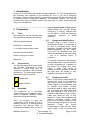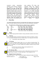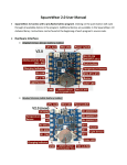
1
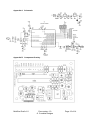
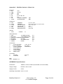
Minifilter
DSP Audio Processor
User Manual
CONTENTS
1
INTRODUCTION
2
2
PREPARATION
2
3
CIRCUIT DESCRIPTION
3
4
ASSEMBLY
4
5
TESTING
6
6
SET UP AND OPERATION
7
APPENDICES
Schematic
Overlay
Parts List
Troubleshooting
Specifications
Template
A
B
C
D
E
F
1 Introduction
Thank you for purchasing the Cumbria Designs “Minifilter” kit. This manual describes
the assembly and operation of the Minifilter kit, even if you are a seasoned
constructor, please read this manual and familiarise yourself with the instructions and
kit contents before commencing soldering. If assembled carefully, this unit will
provide many years of reliable service. We hope that you enjoy constructing and
using your new Minifilter.
________________________________________________________________
uses a double sided Printed Circuit
Board (PCB) with through plating,
2 Preparation
removal of a wrongly soldered part
can be difficult. Follow the assembly
2.1
Tools
instructions
carefully
to
avoid
We recommend that the following tools
mistakes.
are used during assembly and testing;
2.4
25W fine tipped soldering
60/40 Rosin cored solder
5” or smaller diagonal side cutters
Small pointed nosed pliers
Solder sucker (just in case!)
Multimeter
2.2
Conventions
The following symbols are used within
the assembly instructions to draw
attention to critical steps such as
component orientation and anti-static
precautions. The associated narrative
describes the action required.
2.3
!
Critical Step
Static Sensitive
The production of a successful
finished working kit is dependent upon
careful component handling, careful
placement and good soldering!
Don’t be tempted to rush the
construction, even though this is a
relatively simple kit, a wrongly placed
component can provide hours of
frustrating fault finding. Also, as this kit
Minifilter Draft v1.0
All parts carry a coded identity to
describe their values. It is important to
be able to recognise these during
assembly. Capacitors have their value
printed numerically, e.g. 104 = 100nF,
103 = 10nF etc. Resistors have their
values represented by coloured bands
– this is a frequent source of
confusion!
To simplify component identification,
the assembly notes carry the identities
of each component as it appears on
the device. For resistors the colour
coding is given. This should be
referred to during assembly to ensure
the right parts are placed in their
respective positions on the PCB.
2.5
Assembly
Component Identification
Component Leads
Many of the passive components will
require their leads to be formed to
align with the holes on the PCB. This
mainly applies to the axial parts such
as resistors and diodes. Forming
component leads is easily done with a
pair of pointed nose pliers and using
the hole spacing on the PCB as a
measure. Alternatively, small formers
made from scrap off cuts of Vero
board etc., make ideal templates that
produce consistent results. Some
parts, such as variable resistors, have
preformed leads designed for machine
assembly.
These
will
require
straightening to align with the board
layout. Again, a pair of pointed nose
Doc version 1.0
© Cumbria Designs
Page 2 of 14
pliers should be used to carefully
flatten the factory performing to
produce straight leads.
2. Apply the solder allowing it to
flow
smoothly
onto
the
surfaces.
3. Remove the iron and inspect
the new joint.
2.6
Soldering
Before applying solder check carefully
that the component you have
placed is in the right position! This
is a through plated double sided
board. Whilst some of the pads are
very small, the area presented by the
through plating is more than adequate
to allow good solder flow to form
mechanically strong good electrical
joints. However, these can be difficult
to undo, so please double check
placement!
The majority of problems are likely to
be caused by soldering faults. These
can sometimes be difficult to find. Here
are some basic golden rules that will
help you to avoid poor solder joints;
• Clean Iron
Make sure your soldering iron tip is in
good condition and tinned. A small
moistened pad for cleaning tips,
regularly used to wipe off excess
solder and flux, will ensure that your
iron performs well. Remember to tin
the iron immediately after each wipe.
• Clean Leads and Pads
All of the component leads and PCB
pads in this kit are pre-tinned and
should not need cleaning before
soldering. Please ensure that parts are
handled so as to avoid contamination
with grease or fingerprints.
• Soldering
This is the bit that can trip up even
experienced constructors. For the
solder to fuse with the surfaces to be
joined it is necessary for them to be
hot – but not so hot as to damage the
parts! It’s as simple as 1-2-3;
1. Place the tip of the iron against
the joint, hold it there briefly to
bring the metal surfaces up to
temperature.
Minifilter Draft v1.0
The finished joint should have a
smooth shiny coating of solder. If the
joint is dull grey or has formed a
spherical “blob”, apply the iron to the
joint, remove the old solder with a
solder sucker and re-solder.
3
3.1
Circuit Description
General
The Minifilter circuit comprises of three
sections; an input amplifier (MCP618),
a microprocessor (dsPIC33FJ) and an
output amplifier (LM380). The input
amplifier in conjunction with the input
level pot VR1 enables the Minifilter to
operate with a wide range of input
signal voltages. This offer flexibility in
using the Minifilter, allowing it to be
used with low level audio sources such
as AF pre-amp outputs with just a few
tens of millivolts up to higher level
sources such as headphone outputs
which may produce a volt or more of
output. The microprocessor performs
the analogue to digital signal
conversion, the filtering and audio
processing and conversion to from
digital back to analogue to drive the
AF power amplifier. The various
functions of the Minifilter are selected
by grounding the control inputs.
Ground points are provided on the
control header for use with external
switch controls. It is important that no
voltages greater than 3.3V are applied
to these inputs, damage may occur if
this is not observed.
3.2
Theory of Operation
At the heart of the Minifilter is a 16bit
microprocessor with Analogue to
Digital Converter (ADC) and an audio
Digital to Analogue Converter (DAC).
The microprocessor samples the audio
from the input amplifer 8000 times a
second converting the audio voltage to
Doc version 1.0
© Cumbria Designs
Page 3 of 14
numerical
values
representing
amplitude. These values or "samples"
are passed to a Finite Impulse
Response (FIR) filter algorithm that
applies linear phase 511 tap band
pass filtering to the samples. The filter
algorithm is based upon a delay line
where samples are stored and a set of
data called a "kernel" which operates
on the stored samples to produce the
filtered output. The filtered audio
samples are then steered through the
denoiser and auto-notch processes if
selected. These two programs are
almost identical to each other and are
4
short adaptive FIR filters that
constantly adjust their frequency
response to track any repetitive
(coherent) components within the
audio samples. The denoiser output is
the output of the tracking filter, which
because of its narrow bandwidth
reduces random noise. The auto-notch
output is the audio less the output of
the tracking filter causing it to remove
any
constant
coherent
signals.
Processed audio samples are then
passed to the DAC for conversion
back to analogue voltage to drive the
AF
power
amplifier.
Assembly
The following assembly sequence is recommended. This allows most of the smaller
parts to be held in place with the board turned over whilst soldering the underside.
4.1
Fixed Resistors (Broad tolerance band shown in capitals)
2R7
100R
470R
1K
10K
47K
4.2
!
R10
R2, R6
R3
R8
R1, R4, R5, R7
R9
Red, Mauve, Black, Silver (BROWN)
Brown, Black, Black, Black, (BROWN)
Yellow, Mauve, Black, Black (BROWN)
Brown, Black, Black, Brown, (BROWN)
Brown, Black, Black, Red, (BROWN)
Yellow, Mauve, Black, Red, (BROWN)
Diode
Fit the 1N4004 supply protection diode D1 noting orientation marked on silk screen.
4.3
Inductor
Fit the 15uH axial inductor (resembles a large brown resistor) in position L1 next to
D1. Form leads at 90 degrees close to inductor body so as to align with PCB holes.
L1
4.4
!
IC Sockets
Ensure correct orientation! Match index cut out on socket to board printing. Tip;
solder one pin only then check positioning before continuing. Heat the solder and
reposition if necessary. Two 14 pin sockets are provided to make the 28 pin socket
required for IC3.
a)
b)
4.5
!
15uH Brown, Green, Black, Silver
Fit the 2x14 pin sockets in 28 pin socket position for IC3.
Fit 8 pin sockets for IC4 and IC5.
SIL Resistor RN1
The orientation of the 10K SIL resistor is critical. Install with the text side of the SIL
package facing IC3 sockets. The spot marking pin 1 will be adjacent to C8.
4.6
Dipped Ceramic Capacitors
Small yellow body, 0.1” pitch. Used general signal coupling and supply decoupling.
Minifilter Draft v1.0
Doc version 1.0
© Cumbria Designs
Page 4 of 14
100nF C2, C4, C5, C6, C7, C8, C9, C19
4.7
104
Ceramic Capacitors
Standard brown body disk ceramics are used for decoupling +12V supply input,
audio input and AF amplifier input.
10nF
4.8
103Z
C1, C11, C14
Variable Cermet Resistor
The pre-formed leads will require to be straightened to fit. Remove the corrugations
by gently compressing each lead with a pair of small pliers.
10K Audio Input Cermet
4.9
!
VR1
103
+3V3 Regulator
Polarity conscious component, ensure that orientation is correct. Carefully form leads
so as to be able to insert the TO92 style regulator into IC2 position taking care to
align the body and leads with the outline marked on the silk screen.
3v3 regulator IC2
4.10
MCP1700
Polystyrene Capacitors
Rectangular body, no polarity.
0.47uF
4.11
!
C12, C16, C17
u47
Electrolytic Capacitors
Polarised Capacitors, observe the polarity shown by the silk screen. The negative
lead is marked by a stripe on the capacitor body.
10uF C3, C10
100uF C13, C15
4.12 Connectors
Recommended Pin Header Connector orientation is with rear locking tab facing into
the centre of the board. The AF Gain header is mount with rear tab adjacent to IC5.
a)
b)
c)
Fit the two, two pin headers
Fit the three way AF Gain header
Fit the twelve way Controls header
+12V, AF, LS
AF_GAIN
4.13 +5V Regulator
!
Polarity conscious component, ensure that orientation is correct. The regulator is
mounted vertically with the metal face towards the outside edge of the PCB. Heatsink
not required.
+5V regulator IC1
MC7805CT
4.14 Integrated Circuits
!
Static sensitive parts. Discharge yourself to ground before handling. Avoid wearing
static generating clothing (e.g. wool, man made fibres etc) during assembly.
Minifilter Draft v1.0
Doc version 1.0
© Cumbria Designs
Page 5 of 14
Correct orientation is essential. IC pins will need to be gently formed for correct
alignment before insertion into sockets. IC pins can be pushed inwards by placing the
device on its’ side on a firm surface, and gently pressing the body down against the
pins. When inserting parts, take care to check pin alignment to prevent damage.
a)
b)
c)
4.15
Insert IC3
Insert IC4
Insert IC5
dsPIC33F128GP802 Processor (28 pin DIL)
MCP618
Operational Amplifier
LM380N-8
AF Power Amplifier
Connector Assemblies
Connector shells and pins are supplied to allow connection of power and signal lines
to the Microcode DSP. The use of good quality, colour coded, heat resistant, multi
stranded wire is recommended. To avoid accidents, a colour code convention should
be chosen to represent function, e.g. Red +ve supply, Black ground, striped colours
controls etc.
The connector assemblies comprise of two components; the shell and the pins. To
terminate a conductor first strip back about 2mm of insulation and tin the exposed
wire. Place the tinned end of the wire into a pin such that the tinned wire sits inside
the inner pair of tabs and the insulation sits within the outer tabs. With small pointed
nose pliers carefully compress the outer tabs onto the insulation to hold the wire.
Repeat this with the inner tabs to grip the exposed conductor. Very carefully solder
the exposed conductor in place taking care not to allow solder to flow onto the
locking tab.
Finally, insert the pin into the shell with the small locking tab orientated to the face of
the shell with the small cut outs. Push home until the locking tab snaps into the cut
out. Should you need to remove a pin, gently press the locking tab in with a small
screwdriver or the end of a pair of pointed nose pliers. The pin will be released and
can be pulled out of the shell.
Assembly complete, well done! Now carefully check the component
placement and soldering work before moving on to testing.
5
TESTING
Before connecting your Minifilter to your power supply for the first time, carry out
these simple checks to confirm that the supply rails are clear of shorts to ground.
5.1
Electrical Tests
5.1.1 +12 Volt Input
With a multimeter set to resistance, place the Red meter lead onto +12v and the
Black to Ground and check for a high resistance. Providing there is not a short circuit
then all is well.
5.1.2 +5 Volt Rail
Carry out the resistance test on the output side of the regulator (IC1) to check the
+5v rail ensuring that it is clear of shorts to ground.
5.1.3 +3.3 Volt Rail
Carry out the resistance test on the output side of the regulator (IC2) to check the
+3.3v rail ensuring that it is clear of shorts to ground.
Minifilter Draft v1.0
Doc version 1.0
© Cumbria Designs
Page 6 of 14
5.1.4 Powering Up
Connect a loudspeaker and AF gain potentiometer (10K log) as shown in Fig.1
6
SET UP AND OPERATION
6.1
Power and Audio Connections
Signal
Speaker
AF Source
Volume
Control
Screen
Ground
+12V
Controls
Fig. 1 Power and Audio Connections
6.1.1 Loud Speaker
The audio output should be connected to a 4 to 8 Ohm impedance loudspeaker.
6.1.2 AF Gain Potentiometer
The AF Gain potentiometer is connected as shown above. This will produce
increasing audio output with clockwise rotation.
6.1.3 AF Input
A screened audio cable should be used to connect the signal source to the AF Input
connector.
6.1.4 Power
Connect +12V to the power header observing the polarity shown above. Advancing
the AF Gain control should produce a noticeable hiss from the loudspeaker. If
nothing is heard disconnect and check the supply, loudspeaker and AF Gain control
wiring. Check the orientation and placement of all ICs and electrolytic capacitors.
Minifilter Draft v1.0
Doc version 1.0
© Cumbria Designs
Page 7 of 14
6.2
Controls Header
GND AN
GND
GND
DEN
GND
GRP
FL1..FL4
6.2.1
GND DEN GND GRP GND FL5 FL4 FL3 FL2 FL1
Ground supply pin for external switch
Ground supply pin for external switch
Denoiser, high = denoiser off , low = denoiser on
Ground supply pin for external switch
Filter Group, high = wide, low = narrow
Filter select bits
Filter Selection Controls
1=Open circuit or +3.3V logic high
0=Ground or logic low
GRP FL5 FL4 FL3 FL2 FL1
Wide Filter Group
1
1
1
1
1
1
1
1
1
1
1
0
1
1
1
1
0
1
1
1
1
0
1
1
1
1
0
1
1
1
1
0
1
1
1
1
Narrow Filter Group
0
1
1
1
1
1
0
1
1
1
1
0
0
1
1
1
0
1
0
1
1
0
1
1
0
1
0
1
1
1
0
0
1
1
1
1
FILTER
300 - 2700Hz
300 - 2400Hz
300 - 2200Hz
400 - 2200Hz
400 - 2100Hz
450 - 2000Hz
400 - 900Hz
450 - 850Hz
500 - 800Hz
600 - 800Hz
500 - 700Hz
400 - 600Hz
6.2.2 Denoiser and Auto-notch Controls
1=Open circuit or +3.3V logic high
0=Ground or logic low
AN DEN
Audio Processing
1
1
No audio processing
1
0
Denoiser
0
1
Auto-notch
0
0
Denoiser and Auto-notch
6.3
Control Options
Important! All Minifilter control inputs must be treated as "voltage free" inputs. In
other words they should only be operated by switches or devices such as open
collector transistors so as not to apply an external voltage to the control port. With no
control conditions applied all pins are held high at 3.3V by the 10K SIL pull up
resistor. The ground pins provided on the control port should be used as the switched
0V reference to pull any pin into a logic low state.
The flexibility of the simple control interface allows many control scheme options.
Several examples are given below.
Minifilter Draft v1.0
Doc version 1.0
© Cumbria Designs
Page 8 of 14
6.3.1
Switched Control Schemes
Fig.2 Basic Controls
A single pole 6 way rotary switch and three toggle switches are used to access all of
the control states.
Fig.3 Using a rotary switch for Audio Processing controls
A 2 pole 4 way rotary switch replaces two toggle switches for Denoiser and Autonotch control.
Minifilter Draft v1.0
Doc version 1.0
© Cumbria Designs
Page 9 of 14
Fig.4 Set of filters from both groups selected by rotary switch
A two pole rotary switch provides selection of filters from both wide and narrow filter
groups.
6.3.2
Microprocessor Control
The filter and audio processing bits may be controlled by an 8 bit wide port of an
external microprocessor. Care must be taken to ensure that the logic high voltage of
+3.3V used by the Minifilter is not exceeded. If the external microprocessor uses
3.3V logic then direct connection is possible. Ensure that the microprocessor and
the Minifilter share a common ground.
If the external microprocessor logic voltage is +5V then provision must be made to
protect the +3.3V control port of the Minifilter. This is conveniently done with general
purpose diodes (1N4148, BAV21 etc) placed between the external microprocessor
port and the Minifilter control port. The diodes are oriented with their cathodes (band)
towards the higher voltage external microprocessor port to block any current from
flowing into the Minifilter port during a logic high state. The SIL pull up resistor on the
Minifilter control port will hold the control inputs at +3.3V.
6.4
Input Level
The input level is set by adjusting VR1, start with VR1 set fully anticlockwise. If
connecting to a point where the level is variable, e.g. a headphone socket on a
receiver whose output is set by the receiver AF gain control, adjust the receiver
output to normal listening level. Next, connect the Minifilter and adjust VR1 slowly
clockwise (ensuring the Minifilter AF Gain is turned up so as to produce an output)
until audio is heard. Continue until the audio distorts slightly (clipping). Back off VR1
below the clipping level.
If the Minifilter is to be used as a replacement audio section in a receiver it should be
connected to the output of the AF pre-amp stage before the receiver's AF gain
control. The receiver's AF gain control may be used as the Minifilter AF gain control
by wiring it as shown in Fig.1.
Minifilter Draft v1.0
Doc version 1.0
© Cumbria Designs
Page 10 of 14
6.5
Operating Notes
The following points will help you to get the best performance from your Minifilter;
• Set the Minifilter input level just below that which causes clipping - evident as
a "crackling" on audio peaks. Maintaining a high input level improves the
performance of the denoiser and auto-notch.
• The denoiser operates on random noise only, any noise source with a cyclical
content will not be suppressed.
• Use the steep edges of the audio filters to remove adjacent signals that are
encroaching into the passband. For example, if an adjacent signal is causing
high frequency audio interference within the passband switch to the next
narrower filter to lower the cut off frequency.
Minifilter Draft v1.0
Doc version 1.0
© Cumbria Designs
Page 11 of 14
Appendix A Schematic
Appendix B Component Overlay
Minifilter Draft v1.0
Doc version 1.0
© Cumbria Designs
Page 12 of 14
Appendix C Minifilter Version 1.0 Parts List
Resistors
1 2R7
2 100R
1 470R
1 1K
4 10K
1 47K
1 10K
1 10kx8
R10
R2, R6
R3
R8
R1, R4, R5, R7
R9
CERMET TRIMMER
SIL RESISTOR
VR1
RN1
Capacitors
3 10nF
8 100nF
3 0.47uF
1 10uF
2 10uF
2 100uF
CERAMIC
CERAMIC
POLYSTYRENE
TANTALUM
ELECTROLYTIC
ELECTROLYTIC
C1, C11, C14
C2, C4, C5, C6, C7, C8, C9, C19
C12, C16, C17
C18
C3, C10
C13, C15
Inductor
1 15uH
CHOKE
L1
Semiconductors
1 7805
+5V REGULATOR
1 MCP1700
+3V3 REGULATOR
1 DSPIC33FJ128GP802 PROCESSOR
1 MCP618P
OP AMP
1 LM380N-8
AF POWER AMP
1 1N4004
DIODE
Connectors
3
2 WAY HEADER
1
3 WAY HEADER
1
12 WAY HEADER
3
2 WAY SHELLS
1
3 WAY SHELL
1
12 WAY SHELL
21
CRIMP PINS
IC Sockets
2
8 PIN DIL
2
14 PIN DIL
Misc
PCB
IC1
IC2
IC3
IC4
IC5
D1
+12V, AF, LS
AF_GAIN
CONTROLS
IC4, IC5
IC3
Minifilter v1.0
APPENDIX D Specifications
Dimensions
W66mm, H47mm, D22mm (Overall with connectors fitted)
Supply Voltage
Nominal +10V to +20V
Supply Current
54mA
Operating Temperature -20ºC to +70ºC
Minifilter Draft v1.0
Doc version 1.0
© Cumbria Designs
Page 13 of 14
Appendix E
Troubleshooting
Symptom
No audio output
Controls not functioning correctly
Audio distorted
Appendix F
Action
Confirm supply on pin 7 and ground
on pin 4 of IC5
Check IC5 placement, soldering and
orientation, check soldering and
orientation of electrolytics
Check soldering of AF Gain header
and wiring to AF gain pot
Confirm continuity and soldering of
C16 and R9 and pin 23 of IC3
Check soldering on controls header
and associated IC3 pins
Remove controls and confirm input
pins at 3.3V
Check orientation of RN1
Check ground condition is being
applied as per tables in Section 6.2
Reduce input level by turning VR1
anticlockwise
Check orientation of C18
Mark through template for preparing enclosure. Use centres as
guides, check and edit positions before drilling and cutting.
END
Minifilter Draft v1.0
Doc version 1.0
© Cumbria Designs
Page 14 of 14