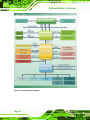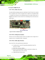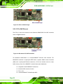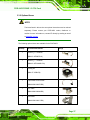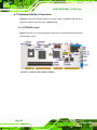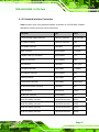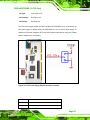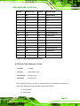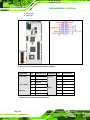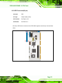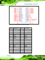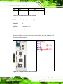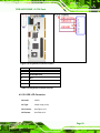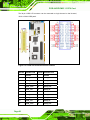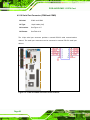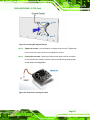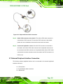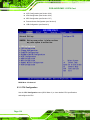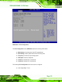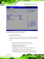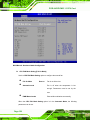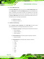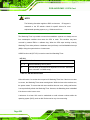
1
PCIE-9452 PICMG 1.3 CPU Card
Page i
PCIE-9452 PICMG 1.3 CPU Card
Revision
Date
Version
Changes
2007-08-23
1.10
CF Compatibility enhanced
Added “Appendix F: Hazardous Materials Disclosure”
Changed all Socket 479 to Socket M
2007-05-02
Page ii
1.00
Initial release
PCIE-9452 PICMG 1.3 CPU Card
Manual Conventions
WARNING!
Warnings appear where overlooked details may cause damage to the equipment or result
in personal injury. Warnings should be taken seriously. Warnings are easy to recognize.
The word “warning” is written as “WARNING,” both capitalized and bold and is followed by
text. The text is the warning message. A warning message is shown below:
WARNING:
This is an example of a warning message. Failure to adhere to warning
messages may result in permanent damage to the PCIE-9452 or
personal injury to the user. Please take warning messages seriously.
CAUTION!
Cautionary messages should also be heeded to help reduce the chance of losing data or
damaging the PCIE-9452. Cautions are easy to recognize. The word “caution” is written
as “CAUTION,” both capitalized and bold and is followed. The italicized text is the
cautionary message. A caution message is shown below:
Page iii
PCIE-9452 PICMG 1.3 CPU Card
CAUTION:
This is an example of a caution message. Failure to adhere to cautions
messages may result in permanent damage to the PCIE-9452. Please
take caution messages seriously.
NOTE:
These messages inform the reader of essential but non-critical information. These
messages should be read carefully as any directions or instructions contained therein can
help avoid making mistakes. Notes are easy to recognize. The word “note” is written as
“NOTE,” both capitalized and bold and is followed by text. The text is the cautionary
message. A note message is shown below:
NOTE:
This is an example of a note message. Notes should always be read.
Notes contain critical information about the PCIE-9452. Please take
note messages seriously.
Page iv
PCIE-9452 PICMG 1.3 CPU Card
Copyright
COPYRIGHT NOTICE
The information in this document is subject to change without prior notice in order to
improve reliability, design and function and does not represent a commitment on the part
of the manufacturer.
In no event will the manufacturer be liable for direct, indirect, special, incidental, or
consequential damages arising out of the use or inability to use the product or
documentation, even if advised of the possibility of such damages.
This document contains proprietary information protected by copyright. All rights are
reserved. No part of this manual may be reproduced by any mechanical, electronic, or
other means in any form without prior written permission of the manufacturer.
TRADEMARKS
All registered trademarks and product names mentioned herein are used for identification
purposes only and may be trademarks and/or registered trademarks of their respective
owners.
Page v
PCIE-9452 PICMG 1.3 CPU Card
Packing List
NOTE:
If any of the components listed in the checklist below are missing,
please do not proceed with the installation. Contact the IEI reseller or
vendor you purchased the PCIE-9452 from or contact an IEI sales
representative directly. To contact an IEI sales representative, please
send an email to [email protected].
The items listed below should all be included in the PCIE-9452 package.
1 x PCIE-9452 single board computer
1 x IDE cable
2 x SATA power cable
4 x SATA cables
1 x Dual RS-232 cable
1 x USB cable
1 x Mini jumper pack
1 x Utility CD
1 x 1 x QIG (quick installation guide)
Images of the above items are shown in Chapter 3.
Page vi
PCIE-9452 PICMG 1.3 CPU Card
Table of Contents
1
INTRODUCTION..................................................................................................... 1
1.1 INTRODUCTION .......................................................................................................... 2
1.1.1 PCIE-9452 Benefits ........................................................................................... 2
1.1.2 PCIE-9452 Features .......................................................................................... 2
1.2 PCIE-9452 OVERVIEW .............................................................................................. 3
1.2.1 PCIE-9452 Overview Photo .............................................................................. 3
1.2.2 PCIE-9452 Peripheral Connectors and Jumpers .............................................. 3
1.2.3 Technical Specifications..................................................................................... 4
2
DETAILED SPECIFICATIONS ............................................................................. 7
2.1 OVERVIEW ................................................................................................................. 8
2.2 DIMENSIONS .............................................................................................................. 8
2.2.1 Board Dimensions.............................................................................................. 8
2.2.2 External Interface Panel Dimensions ................................................................ 9
2.3 DATA FLOW ................................................................................................................ 9
2.4 COMPATIBLE PROCESSORS ........................................................................................11
2.4.1 Compatible Processor Overview ......................................................................11
2.4.2 Supported Processors .......................................................................................11
2.5 INTEL® 945GM NORTHBRIDGE CHIPSET.................................................................. 12
2.5.1 Intel® 945GM Overview................................................................................... 12
2.5.2 Intel® 945GM Memory Support ....................................................................... 13
2.5.3 Intel® 945GM PCIe x16 ................................................................................... 14
2.5.3.1 PCIe x16 Bus Overview............................................................................ 14
2.5.3.2 PCIe x16 Expansion Options .................................................................... 14
2.5.3.3 PCIe x16 Bus Specifications..................................................................... 14
2.5.4 Intel® 945GM Integrated Graphics ................................................................. 15
2.5.4.1 Intel® 945GM Analog CRT Support ......................................................... 15
2.5.4.2 Intel® 945GM LVDS Support ................................................................... 15
2.5.4.3 Intel® 945GM TV Out Support................................................................. 16
2.5.5 Intel® 945GM Direct Media Interface (DMI) .................................................. 16
2.6 INTEL® ICH7R SOUTHBRIDGE CHIPSET ................................................................... 17
Page vii
PCIE-9452 PICMG 1.3 CPU Card
2.6.1 Intel® ICH7R Overview.................................................................................... 17
2.6.2 Intel® ICH7R Audio Codec ’97 Controller ...................................................... 17
2.6.3 Intel® ICH7R IDE Interface............................................................................. 18
2.6.4 Intel® ICH7R Low Pin Count (LPC) Interface ................................................ 19
2.6.5 Intel® ICH7R PCI Interface ............................................................................. 19
2.6.6 Intel® ICH7R Real Time Clock ........................................................................ 19
2.6.7 Intel® ICH7R SATA Controller......................................................................... 19
2.6.8 Intel® ICH7R USB Controller.......................................................................... 20
2.6.8.1 Intel® ICH7R USB Controller Overview.................................................. 20
2.6.8.2 PCIE-9452 USB Implementation ............................................................. 20
2.6.8.3 Backplane USB Implementation............................................................... 20
2.6.9 Intel® ICH7R PCIe Bus.................................................................................... 21
2.6.9.1 Intel® ICH7R PCIe Bus Overview............................................................ 21
2.6.9.2 PCIe x4 Expansion Options ...................................................................... 21
2.6.9.3 PCIe GbE Ethernet.................................................................................... 22
2.7 LPC BUS COMPONENTS ........................................................................................... 23
2.7.1 LPC Bus Overview........................................................................................... 23
2.7.2 BIOS Chipset.................................................................................................... 23
2.7.3 Super I/O chipset.............................................................................................. 24
2.7.3.1 Super I/O LPC Interface ........................................................................... 25
2.7.3.2 Super I/O 16C550 UARTs ........................................................................ 25
2.7.3.3 Super I/O Enhanced Hardware Monitor ................................................... 25
2.7.3.4 Super I/O Fan Speed Controller................................................................ 25
2.7.3.5 Super I/O Parallel Port .............................................................................. 26
2.7.3.6 Super I/O Keyboard Controller................................................................. 26
2.8 ENVIRONMENTAL AND POWER SPECIFICATIONS ....................................................... 26
2.8.1 System Monitoring ........................................................................................... 26
2.8.2 Operating Temperature and Temperature Control........................................... 27
2.8.3 Power Consumption......................................................................................... 28
2.9 EXPANSION OPTIONS ................................................................................................ 28
2.9.1 Expansion Options Overview........................................................................... 28
2.9.2 IEI Expansion PICMG 1.3 Backplanes ........................................................... 28
2.9.3 IEI Chassis ....................................................................................................... 29
3
UNPACKING .......................................................................................................... 33
Page viii
PCIE-9452 PICMG 1.3 CPU Card
3.1 ANTI-STATIC PRECAUTIONS ...................................................................................... 34
3.2 UNPACKING.............................................................................................................. 34
3.2.1 Unpacking Precautions.................................................................................... 34
3.3 UNPACKING CHECKLIST ........................................................................................... 35
3.3.1 Package Contents............................................................................................. 35
3.3.2 Optional Items.................................................................................................. 37
4
CONNECTOR PINOUTS...................................................................................... 39
4.1 PERIPHERAL INTERFACE CONNECTORS .................................................................... 40
4.1.1 PCIE-9452 Layout ........................................................................................... 40
4.1.2 Peripheral Interface Connectors ..................................................................... 41
4.1.3 External Interface Panel Connectors............................................................... 42
4.2 INTERNAL PERIPHERAL CONNECTORS ...................................................................... 42
4.2.1 ATX Power Supply Enable Connector ............................................................. 42
4.2.2 Audio Connector (9-pin) .................................................................................. 44
4.2.3 Backlight Inverter Connector .......................................................................... 46
4.2.4 Compact Flash Socket...................................................................................... 47
4.2.5 Digital Input/Output (DIO) Connector............................................................ 50
4.2.6 Fan Connector (+12V) .................................................................................... 51
4.2.7 Floppy Disk Connector (34-pin)...................................................................... 52
4.2.8 Front Panel Connector (14-pin) ...................................................................... 53
4.2.9 IDE Connector(40-pin).................................................................................... 55
4.2.10 Infrared Interface Connector (5-pin) ............................................................. 57
4.2.11 Keyboard Connector ...................................................................................... 58
4.2.12 LVDS LCD Connector ................................................................................... 59
4.2.13 Mouse Connector ........................................................................................... 61
4.2.14 Parallel Port Connector ................................................................................ 62
4.2.15 SATA Drive Connectors ................................................................................. 64
4.2.16 Serial Port Connector (COM1and COM2).................................................... 66
4.2.17 TV Out Connector .......................................................................................... 67
4.2.18 USB Connectors (Internal) ............................................................................ 68
4.3 EXTERNAL PERIPHERAL INTERFACE CONNECTOR PANEL ......................................... 70
4.3.1 LAN Connectors............................................................................................... 70
4.3.2 USB Connector ................................................................................................ 71
4.3.3 VGA Connector ................................................................................................ 72
Page ix
PCIE-9452 PICMG 1.3 CPU Card
5
INSTALLATION .................................................................................................... 75
5.1 ANTI-STATIC PRECAUTIONS ...................................................................................... 76
5.2 INSTALLATION CONSIDERATIONS ............................................................................. 77
5.2.1 Installation Notices .......................................................................................... 77
5.2.2 Installation Checklist ....................................................................................... 78
5.3 CPU, CPU COOLING KIT AND DIMM INSTALLATION ............................................. 79
5.3.1 Socket M CPU Installation .............................................................................. 79
5.3.2 Cooling Kit CF-479B-RS Installation.............................................................. 82
5.3.3 DIMM Installation ........................................................................................... 84
5.3.4 CF Card Installation........................................................................................ 85
5.4 JUMPER SETTINGS .................................................................................................... 87
5.4.1 CF Card Setup ................................................................................................. 88
5.4.2 Clear CMOS Jumper........................................................................................ 89
5.4.3 LVDS Voltage Selection.................................................................................... 91
5.5 CHASSIS INSTALLATION ........................................................................................... 92
5.5.1 Airflow.............................................................................................................. 92
5.5.2 Backplane Installation ..................................................................................... 93
5.5.3 CPU Card Installation ..................................................................................... 93
5.6 INTERNAL PERIPHERAL DEVICE CONNECTIONS........................................................ 94
5.6.1 Peripheral Device Cables ................................................................................ 94
5.6.2 IDE Cable Connection..................................................................................... 94
5.6.3 5.1 Channel Audio Kit Installation .................................................................. 95
5.6.4 7.1 Channel Audio Kit Installation .................................................................. 97
5.6.5 Parallel Port Cable.......................................................................................... 98
5.6.6 Dual RS-232 Cable Connection..................................................................... 100
5.6.7 USB Cable (Dual Port).................................................................................. 101
5.6.8 SATA Drive Connection ................................................................................. 102
5.6.9 Wafer-to-PS/2 Cable (Keyboard/Mouse Installation).................................... 104
5.7 EXTERNAL PERIPHERAL INTERFACE CONNECTION ................................................. 105
5.7.1 LAN Connection (Single Connector) ............................................................. 106
5.7.2 USB Device Connection (Single Connector) ................................................. 107
5.7.3 VGA Monitor Connection .............................................................................. 108
6
AMI BIOS.............................................................................................................. 109
6.1 INTRODUCTION .......................................................................................................110
Page x
PCIE-9452 PICMG 1.3 CPU Card
6.1.1 Starting Setup..................................................................................................110
6.1.2 Using Setup .....................................................................................................110
6.1.3 Getting Help.................................................................................................... 111
6.1.4 Unable to Reboot After Configuration Changes............................................. 111
6.1.5 BIOS Menu Bar............................................................................................... 111
6.2 MAIN ......................................................................................................................112
6.3 ADVANCED ..............................................................................................................113
6.3.1 CPU Configuration.........................................................................................114
6.3.2 IDE Configuration ..........................................................................................116
6.3.2.1 IDE Master, IDE Slave ............................................................................117
6.3.3 Floppy Configuration..................................................................................... 123
6.3.4 Super IO Configuration.................................................................................. 124
6.3.5 Hardware Health Configuration.................................................................... 127
6.3.6 ACPI Configuration ....................................................................................... 133
6.3.6.1 General ACPI Configuration................................................................... 134
6.3.7 APM Configuration........................................................................................ 135
6.3.8 MPS Configuration ........................................................................................ 139
6.3.9 Remote Access Configuration ........................................................................ 140
6.3.10 USB Configuration....................................................................................... 144
6.4 PCI/PNP ................................................................................................................ 146
6.5 BOOT ..................................................................................................................... 152
6.5.1 Boot Settings Configuration........................................................................... 152
6.5.2 Boot Device Priority ...................................................................................... 155
6.5.3 Hard Disk Drives ........................................................................................... 157
6.5.4 Removable Drives .......................................................................................... 158
6.5.5 CD/DVD Drives ............................................................................................. 160
6.6 SECURITY............................................................................................................... 162
6.7 CHIPSET ................................................................................................................. 163
6.7.1 NorthBridge Configuration............................................................................ 164
6.7.1.1 Video Function Configuration ................................................................ 169
6.7.2 SouthBridge Chipset Configuration............................................................... 174
6.8 EXIT ....................................................................................................................... 176
7
DRIVER INSTALLATION.................................................................................. 179
7.1 AVAILABLE SOFTWARE DRIVERS ............................................................................ 180
Page xi
PCIE-9452 PICMG 1.3 CPU Card
7.2 DRIVER CD AUTO-RUN .......................................................................................... 180
7.3 CHIPSET DRIVER INSTALLATION............................................................................. 182
7.4 INTEL GRAPHICS MEDIA ACCELERATOR DRIVER ................................................... 187
7.5 BROADCOM LAN DRIVER (FOR GBE LAN) INSTALLATION .................................. 193
7.6 REALTEK HD AUDIO DRIVER (ALC883) INSTALLATION ....................................... 199
7.6.1 BIOS Setup ..................................................................................................... 199
7.6.2 Driver Installation ......................................................................................... 199
7.7 REALTEK AC`97 AUDIO DRIVER (ALC665) INSTALLATION .................................. 203
7.7.1 BIOS Setup ..................................................................................................... 203
7.7.2 Driver Installation ......................................................................................... 203
7.8 INTEL MATRIX STORAGE MANAGER INSTALLATION ................................................211
A
BIOS OPTIONS .................................................................................................... 217
B
DIO INTERFACE................................................................................................. 223
B.1 DIO INTERFACE INTRODUCTION ........................................................................... 224
B.2 DIO CONNECTOR PINOUTS ................................................................................... 224
B.3 ASSEMBLY LANGUAGE SAMPLES ........................................................................... 224
B.3.1 Enable the DIO Input Function..................................................................... 224
B.3.2 Enable the DIO Output Function .................................................................. 225
C
WATCHDOG TIMER .......................................................................................... 227
D
ADDRESS MAPPING.......................................................................................... 231
D.1 ADDRESS MAP ...................................................................................................... 232
D.2 1ST MB MEMORY ADDRESS MAP ......................................................................... 232
D.3 IRQ MAPPING TABLE ............................................................................................ 233
D.4 DMA CHANNEL ASSIGNMENTS ............................................................................. 233
E
INTEL® MATRIX STORAGE MANAGER ..................................................... 235
E.1 INTRODUCTION ...................................................................................................... 236
E.1.1 Precautions .................................................................................................... 236
E.2 FEATURES AND BENEFITS ...................................................................................... 237
E.3 ACCESSING THE INTEL® MATRIX STORAGE MANAGER ......................................... 237
E.4 RAID CONFIGURATION ......................................................................................... 238
E.4.1 Creating a RAID Volume ............................................................................... 238
E.4.2 Deleting a RAID Volume................................................................................ 243
Page xii
PCIE-9452 PICMG 1.3 CPU Card
E.4.3 Resetting a Disk to Non-RAID....................................................................... 245
E.4.4 Exiting the Matrix Storage Manager............................................................. 248
F
HAZARDOUS MATERIALS DISCLOSURE ................................................... 249
F.1 HAZARDOUS MATERIAL DISCLOSURE TABLE FOR IPB PRODUCTS CERTIFIED AS
ROHS COMPLIANT UNDER 2002/95/EC WITHOUT MERCURY ..................................... 250
INDEX............................................................................................................................ 253
Page xiii
PCIE-9452 PICMG 1.3 CPU Card
List of Figures
Figure 1-1: PCIE-9452 Overview [Front View]..............................................................................3
Figure 2-1: PCIE-9452 Dimensions (mm) .....................................................................................8
Figure 2-2: External Interface Panel Dimensions (mm) ..............................................................9
Figure 2-3: Data Flow Block Diagram .........................................................................................10
Figure 2-4: 240-pin DDR2 DIMM Socket .....................................................................................13
Figure 2-5: PCIe x16 Golden Fingers..........................................................................................14
Figure 2-6: Onboard USB Implementation .................................................................................20
Figure 2-7: I/O Golden Finger ......................................................................................................21
Figure 2-8: PCIe x4 Golden finger...............................................................................................22
Figure 2-9: Broadcom PCI GbE Controllers...............................................................................22
Figure 2-10: BIOS Chipset ...........................................................................................................24
Figure 2-11: Super I/O Chipset ....................................................................................................24
Figure 4-1: Connector and Jumper Locations...........................................................................40
Figure 4-2: ATX Power Supply Enable Connector Location ....................................................43
Figure 4-3: Audio Connector Pinouts (10-pin) ...........................................................................45
Figure 4-4: Panel Backlight Connector Pinout Locations ........................................................46
Figure 4-5: CF Card Socket Location .........................................................................................48
Figure 4-6: DIO Connector Connector Locations......................................................................50
Figure 4-7: +12V Fan Connector Location .................................................................................51
Figure 4-8: 34-pin FDD Connector Location ..............................................................................52
Figure 4-9: Front Panel Connector Pinout Locations ...............................................................54
Figure 4-10: Secondary IDE Device Connector Locations .......................................................56
Figure 4-11: Infrared Connector Pinout Locations....................................................................57
Figure 4-12: Keyboard Connector Location ..............................................................................59
Figure 4-13: LVDS LCD Connector Pinout Locations ...............................................................60
Figure 4-14: Mouse Connector Location....................................................................................62
Figure 4-15: Parallel Port Connector Location ..........................................................................63
Figure 4-16: SATA Drive Connector Locations ..........................................................................65
Page xiv
PCIE-9452 PICMG 1.3 CPU Card
Figure 4-17: COM1 and COM2 Connector Pinout Locations ...................................................66
Figure 4-18: TV Connector Pinout Locations ............................................................................68
Figure 4-19: USB Connector Pinout Locations .........................................................................69
Figure 4-20: PCIE-9452 External Peripheral Interface Connector ...........................................70
Figure 4-21: RJ-45 Ethernet Connector......................................................................................71
Figure 4-22: VGA Connector........................................................................................................72
Figure 5-1: Make sure the CPU socket retention screw is unlocked ......................................80
Figure 5-2: Lock the CPU Socket Retention Screw...................................................................81
Figure 5-3: IEI CF-479B-RS Cooling Kit......................................................................................82
Figure 5-4: Cooling Kit Support Bracket ....................................................................................83
Figure 5-5: Connect the cooling fan cable.................................................................................83
Figure 5-6: Installing a DIMM .......................................................................................................84
Figure 5-7: CF Card Installation ..................................................................................................86
Figure 5-8: Jumper Locations .....................................................................................................87
Figure 5-9: CF Card Setup Jumper Location .............................................................................89
Figure 5-10: Clear CMOS Jumper ...............................................................................................90
Figure 5-11: LVDS Voltage Selection Jumper Pinout Locations..............................................92
Figure 5-12: IDE Cable Connection.............................................................................................95
Figure 5-13: 5.1 Channel Audio Kit .............................................................................................96
Figure 5-14: 5.1 Channel Audio Kit .............................................................................................98
Figure 5-15: LPT Cable Connection............................................................................................99
Figure 5-16: Connect the LPT Device ...................................................................................... 100
Figure 5-17: Dual RS-232 Cable Installation ........................................................................... 101
Figure 5-18: Dual USB Cable Connection ............................................................................... 102
Figure 5-19: SATA Drive Cable Connection ............................................................................ 103
Figure 5-20: SATA Power Drive Connection ........................................................................... 104
Figure 5-21: Keyboard/mouse Cable Connection .................................................................. 105
Figure 5-22: LAN Connection ................................................................................................... 106
Figure 5-23: USB Device Connection ...................................................................................... 107
Figure 5-24: VGA Connector..................................................................................................... 108
Figure 6-1: Video Function Configuration............................................................................... 170
Figure 7-1: Introduction Screen ............................................................................................... 181
Page xv
PCIE-9452 PICMG 1.3 CPU Card
Figure 7-2: Available Drivers .................................................................................................... 182
Figure 7-3: Chipset Driver Installation Program..................................................................... 183
Figure 7-4: Chipset Driver Installation Welcome Screen....................................................... 184
Figure 7-5: Chipset Driver Installation License Agreement .................................................. 185
Figure 7-6: Chipset Driver Readme File Information ............................................................. 186
Figure 7-7: Chipset Driver Installation Complete ................................................................... 187
Figure 7-8: Select the Operating System ................................................................................ 188
Figure 7-9: VGA Driver .............................................................................................................. 189
Figure 7-10: GMA Driver Readme File ..................................................................................... 190
Figure 7-11: GMA Driver File Extraction.................................................................................. 190
Figure 7-12: GMA Driver Installation Welcome Screen.......................................................... 191
Figure 7-13: GMA Driver License Agreement ......................................................................... 192
Figure 7-14: GMA Driver Installing Notice............................................................................... 192
Figure 7-15: GMA Driver Installation Complete ...................................................................... 193
Figure 7-16: Access Windows Control Panel ......................................................................... 194
Figure 7-17: Double Click the System Icon............................................................................. 195
Figure 7-18: Double Click the Device Manager Tab ............................................................... 195
Figure 7-19: Device Manager List ............................................................................................ 196
Figure 7-20: Search for Suitable Driver ................................................................................... 197
Figure 7-21: Locate Driver Files ............................................................................................... 198
Figure 7-22: Location Browsing Window ................................................................................ 198
Figure 7-23: 4-AUDIO\AC-KIT883HD\Windows Folder ........................................................... 199
Figure 7-24: HD Audio Driver Setup Extracting Files............................................................. 200
Figure 7-25: HD Audio Driver Setup Welcome Screen........................................................... 201
Figure 7-26: HD Audio Driver Installation Complete .............................................................. 202
Figure 7-27: CD 4-AUDIO\AC-KIT08R\Windows Folder ......................................................... 204
Figure 7-28: AC`97 Audio Driver Install Shield Wizard Starting............................................ 204
Figure 7-29: AC`97 Audio Driver Setup Preparation .............................................................. 205
Figure 7-30: AC`97 Audio Driver Welcome Screen................................................................. 206
Figure 7-31: AC`97 Audio Driver Software Configuration ..................................................... 207
Figure 7-32: AC`97 Audio Driver Digital Signal....................................................................... 208
Figure 7-33: AC`97 Audio Driver Installation Begins ............................................................. 209
Page xvi
PCIE-9452 PICMG 1.3 CPU Card
Figure 7-34: AC`97 Audio Driver Installation Complete ......................................................... 210
Figure 7-35: SATA RAID Driver Installation Program ..............................................................211
Figure 7-36: SATA RAID Setup Program Icon ......................................................................... 212
Figure 7-37: InstallShield Wizard Setup Screen ..................................................................... 212
Figure 7-38: Matrix Storage Manager Setup Screen .............................................................. 213
Figure 7-39: Matrix Storage Manager Welcome Screen ........................................................ 213
Figure 7-40: Matrix Storage Manager Warning Screen .......................................................... 214
Figure 7-41: Matrix Storage Manager License Agreement .................................................... 214
Figure 7-42: Matrix Storage Manager Readme File ................................................................ 215
Figure 7-43: Matrix Storage Manager Setup Complete.......................................................... 216
Page xvii
PCIE-9452 PICMG 1.3 CPU Card
List of Tables
Table 1-1: Technical Specifications ..............................................................................................6
Table 2-1: Processor Features ....................................................................................................11
Table 2-2: Supported Processors ...............................................................................................12
Table 2-3: Supported HDD Specifications..................................................................................18
Table 2-4: Power Consumption ...................................................................................................28
Table 2-5: Compatible IEI PICMG 1.3 Backplanes .....................................................................29
Table 2-6: Compatible IEI Chassis ..............................................................................................31
Table 3-1: Package List Contents................................................................................................36
Table 3-2: Optional Items .............................................................................................................38
Table 4-1: Peripheral Interface Connectors ...............................................................................42
Table 4-2: Rear Panel Connectors ..............................................................................................42
Table 4-3: ATX Power Supply Enable Connector Pinouts ........................................................44
Table 4-4: Audio Connector Pinouts (10-pin).............................................................................45
Table 4-5: Panel Backlight Connector Pinouts ..........................................................................47
Table 4-6: CF Card Socket Pinouts .............................................................................................49
Table 4-7: DIO Connector Connector Pinouts ...........................................................................51
Table 4-8: +12V Fan Connector Pinouts .....................................................................................52
Table 4-9: 34-pin FDD Connector Pinouts..................................................................................53
Table 4-10: Front Panel Connector Pinouts ...............................................................................54
Table 4-11: Secondary IDE Connector Pinouts..........................................................................57
Table 4-12: Infrared Connector Pinouts .....................................................................................58
Table 4-13: Keyboard Connector Pinouts ..................................................................................59
Table 4-14: LVDS LCD Port Connector Pinouts.........................................................................61
Table 4-15: Mouse Connector Pinouts .......................................................................................62
Table 4-16: Parallel Port Connector Pinouts..............................................................................64
Table 4-17: SATA Drive Connector Pinouts................................................................................65
Table 4-18: COM1 and COM2.......................................................................................................67
Table 4-19: TV Port Connector Pinouts ......................................................................................68
Table 4-20: USB Port Connector Pinouts ...................................................................................69
Table 4-21: LAN Pinouts...............................................................................................................70
Table 4-22: RJ-45 Ethernet Connector LEDs .............................................................................71
Page xviii
PCIE-9452 PICMG 1.3 CPU Card
Table 4-23: USB Port Pinouts ......................................................................................................72
Table 4-24: VGA Connector Pinouts ...........................................................................................73
Table 5-1: Jumpers .......................................................................................................................87
Table 5-2: CF Card Setup Jumper Settings................................................................................88
Table 5-3: Clear CMOS Jumper Settings ....................................................................................90
Table 5-4: LVDS Voltage Selection Jumper Settings.................................................................91
Table 5-5: IEI Provided Cables ....................................................................................................94
Table 6-1: BIOS Navigation Keys ..............................................................................................111
Page xix
PCIE-9452 PICMG 1.3 CPU Card
BIOS Menus
Menu 1: Main ...............................................................................................................................112
Menu 2: Advanced ......................................................................................................................114
Menu 3: CPU Configuration.......................................................................................................115
Menu 4: IDE Configuration ........................................................................................................116
Menu 5: IDE Master and IDE Slave Configuration...................................................................118
Menu 6: Floppy Configuration.................................................................................................. 123
Menu 7: Super IO Configuration .............................................................................................. 124
Menu 8: Hardware Health Configuration ................................................................................. 128
Menu 9: ACPI Configuration ..................................................................................................... 133
Menu 10: General ACPI Configuration [Advanced\ ACPI Configuration] ............................ 134
Menu 11:Advanced Power Management Configuration ........................................................ 136
Menu 12: MPS Configuration.................................................................................................... 139
Menu 13: Remote Access Configuration [Advanced] ............................................................ 140
Menu 14: USB Configuration.................................................................................................... 144
Menu 15: PCI/PnP Configuration ............................................................................................. 147
Menu 16: Boot ............................................................................................................................ 152
Menu 17: Boot Settings Configuration .................................................................................... 153
Menu 18: Boot Device Priority Settings .................................................................................. 156
Menu 19: Hard Disk Drives ....................................................................................................... 158
Menu 20: Removable Drives..................................................................................................... 159
Menu 21: CD/DVD Drives .......................................................................................................... 161
Menu 22: Security ...................................................................................................................... 162
Menu 23: Chipset ....................................................................................................................... 164
Menu 24:NorthBridge Chipset Configuration ......................................................................... 165
Menu 25:SouthBridge Chipset Configuration......................................................................... 174
Menu 26:Exit............................................................................................................................... 176
Page xx
PCIE-9452 PICMG 1.3 CPU Card
Glossary
AC ’97
Audio Codec 97
HDD
Hard Disk Drive
ACPI
Advanced Configuration and
IDE
Integrated Data Electronics
Power Interface
I/O
Input/Output
APM
Advanced Power Management
ICH4
I/O Controller Hub 4
ARMD
ATAPI Removable Media Device
L1 Cache Level 1 Cache
ASKIR
Shift Keyed Infrared
L2 Cache Level 2 Cache
ATA
Advanced Technology
LCD
Liquid Crystal Display
Attachments
LPT
Parallel Port Connector
BIOS
Basic Input/Output System
LVDS
Low Voltage Differential Signaling
CFII
Compact Flash Type 2
MAC
Media Access Controller
CMOS
Complementary Metal Oxide
OS
Operating System
Semiconductor
PCI
Peripheral Connect Interface
CPU
Central Processing Unit
PIO
Programmed Input Output
Codec
Compressor/Decompressor
PnP
Plug and Play
COM
Serial Port
POST
Power On Self Test
DAC
Digital to Analog Converter
RAM
Random Access Memory
DDR
Double Data Rate
SATA
Serial ATA
DIMM
Dual Inline Memory Module
S.M.A.R.T Self Monitoring Analysis and
DIO
Digital Input/Output
DMA
Direct Memory Access
SPD
Serial Presence Detect
EIDE
Enhanced IDE
S/PDI
Sony/Philips Digital Interface
EIST
Enhanced Intel SpeedStep
SDRAM
Synchronous Dynamic Random
Reporting Technology
Access Memory
Technology
FDD
Floppy Disk Drive
SIR
Serial Infrared
FDC
Floppy Disk Connector
UART
Universal Asynchronous
FFIO
Flexible File Input/Output
FIFO
First In/First Out
USB
Universal Serial Bus
FSB
Front Side Bus
VGA
Video Graphics Adapter
IrDA
Infrared Data Association
Receiver-transmitter
Page xxi
PCIE-9452 PICMG 1.3 CPU Card
THIS PAGE IS INENTIONALLY LEFT BLANK
Page xxii
PCIE-9452 PICMG 1.3 CPU Card
Chapter
1
1 Introduction
Page 1
PCIE-9452 PICMG 1.3 CPU Card
1.1 Introduction
The PCIE-9452 PICMG 1.3 CPU card is a Socket M Intel® Core™2 Duo, Intel® Core™
Duo, Intel® Core™ Solo or Intel® Celeron M (Yohan core) CPU platform. The PCIE-9452
has a maximum front side bus (FSB) frequency of 667MHz and supports 667MHz 2GB
dual channel memory modules. The PCIE-9452 also comes with multiple display option,
dual PCI Express (PCIe) Gigabit Ethernet (GbE) and has flexible storage options including
support for four second-generation serial ATA (SATA) hard disk drives (HDD), two IDE
HDD, a CompactFlash® Type II (CF Type II) disk, and a floppy disk drive (FDD).
1.1.1 PCIE-9452 Benefits
Some of the PCIE-9452 benefits are listed below:
Multiple display output options
Storage flexibility with support for SATA II drives, IDE drives and CF Type II
disks
DDR2 support enables faster data transfers
Multiple I/O interfaces provide connectivity to a broad range of external
peripheral devices
1.1.2 PCIE-9452 Features
Some of the PCIE-9452 features are listed below.
Support for the following Socket M processors:
o
o
o
o
Intel® Core™2 Duo
Intel® Core™ Duo
Intel® Core™ Solo
Intel® Celeron M
Maximum FSB of 667MHz
Maximum of 4GB dual-channel memory supported with two 240-pin dual
channel 400MHz, 533MHz or 667MHz 2GB DDR2 DIMMs
Four SATA II drives with transfer rates of 3.0Gb/s supported
Intel® Matrix Storage Manager
High performance PCIe GbE Ethernet controllers
Page 2
PCIE-9452 PICMG 1.3 CPU Card
Six USB 2.0 devices supported
Multiple display options including CRT, 18-bit dual-channel LVDS and HDTV
PICMG 1.3 form factor
RoHS compliant
1.2 PCIE-9452 Overview
1.2.1 PCIE-9452 Overview Photo
The PCIE-9452 has a wide variety of internal and external peripheral connectors. A
labeled photo of the peripheral connectors on the front of the PCIE-9452 is shown in
Figure 1-1.
Figure 1-1: PCIE-9452 Overview [Front View]
1.2.2 PCIE-9452 Peripheral Connectors and Jumpers
The PCIE-9452 has the following connectors on-board:
1 x Audio connector
1 x Backplane power connector
1 x Compact flash connector
1 x Digital input/output connector
1 x Fan connector
1 x Floppy disk drive (FDD) connector
1 x Front panel connector
1 x IDE disk drive connector
1 x Infrared interface connector
Page 3
PCIE-9452 PICMG 1.3 CPU Card
1 x Inverter connector
1 x Keyboard connector
1 x LVDS connector
1 x Mouse connector
2 x Serial port connectors (internal COM 1 and COM 2 RS-232)
1 x Parallel port connector
4 x Serial ATA (SATA) drive connectors
1 x TV output connector
2 x USB connectors
The PCIE-9452 has the following external peripheral interface connectors on the board
rear panel
2 x Ethernet connectors
2 x USB port connectors
1 x VGA connector
The PCIE-9452 has the following on-board jumpers:
Clear CMOS
LCD voltage selector
CF card setting
1.2.3 Technical Specifications
PCIE-9452 technical specifications are listed in Table 1-1. See Chapter 2 for details.
Specification
PCIE-9452
Form Factor
PICMG 1.3
Socket M Intel® Core™2 Duo
Socket M Intel® Core™ Duo
System CPU
Socket M Intel® Core™ Solo
Socket M Intel® Celeron M (Yonah core)
Front Side Bus
Page 4
400MHz, 533Mhz, or 667MHz
PCIE-9452 PICMG 1.3 CPU Card
Specification
PCIE-9452
Northbridge: Intel® 945GM
System Chipset
Southbridge: Intel® ICH7R
Two 240-pin DIMM sockets support two dual-channel
Memory
400MHz, 533MHz or 667MHz DDR2 DIMMs with a maximum
capacity of 2GB each
CRT: Integrated in the Intel® 945GM to support CRT
LVDS: Dual channel 18-bit LVDS LCD panel
Display
HDTV: Supports resolutions up to 1080i / 1080P by
component interface
BIOS
AMI Flash BIOS
Audio
7.1 channel or 5.1 channel audio with an optional AC-KIT
LAN
Dual PCIe GbE Broadcom BCM5787M chipsets
COM
Two RS-232 serial ports
Eight USB 2.0 devices supported, two on the bracket, two by
USB2.0
pin header on board and four on the backplane
IDE
One 40-pin IDE connects to two Ultra ATA33/66/100 devices
Floppy Disk Drive
One FDD connector connects to a single FDD
SATA
Four 3.0Gb/s SATA drives supported
One 5-pin connector connects to a keyboard
Keyboard/mouse
One 5-pin connector connects to a mouse
Super I/O
ITE IT8712F
Digital I/O
One 8-bit digital I/O connector (4-bit input / 4-bit output)
Infrared
One Infrared connector
Page 5
PCIE-9452 PICMG 1.3 CPU Card
Specification
PCIE-9452
SSD
CF Type II
Watchdog Timer
Software programmable 1-255 sec. by super I/O
Power Supply
ATX supported
Temperature
0ºC – 60ºC (32ºF - 140ºF)
Humidity (operating)
5%~95% non-condensing
Dimensions (LxW)
338mm x 126mm
Weight (GW/NW)
1100g/ 380g
Table 1-1: Technical Specifications
Page 6
PCIE-9452 PICMG 1.3 CPU Card
Chapter
2
2 Detailed Specifications
Page 7
PCIE-9452 PICMG 1.3 CPU Card
2.1 Overview
This chapter describes the specifications and on-board features of the PCIE-9452 in
detail.
2.2 Dimensions
2.2.1 Board Dimensions
The dimensions of the board are listed below:
Length:
338mm
Width:
126mm
Figure 2-1: PCIE-9452 Dimensions (mm)
Page 8
PCIE-9452 PICMG 1.3 CPU Card
2.2.2 External Interface Panel Dimensions
External peripheral interface connector panel dimensions are shown in Figure 2-2.
Figure 2-2: External Interface Panel Dimensions (mm)
2.3 Data Flow
Figure 2-3 shows the data flow between the two on-board chipsets and other components
installed on the motherboard and described in the following sections of this chapter.
Page 9
PCIE-9452 PICMG 1.3 CPU Card
Figure 2-3: Data Flow Block Diagram
Page 10
PCIE-9452 PICMG 1.3 CPU Card
2.4 Compatible Processors
2.4.1 Compatible Processor Overview
The PCIE-9452 supports the following Socket M processors:
Intel® Core™2 Duo Mobile processors
Intel® Core™ Duo processors
Intel® Core™ Solo processors
Intel® Celeron® M processors
All three of the above processors communicate with the Intel
®
945GM northbridge chipset
through a 667MHz front side bus (FSB). Features of the supported processors are listed in
Table 2-1.
CPU Features
Core™2 Duo Mobile
Core™ Duo
Core™ Solo
Celeron® M
Dual core
Yes
Yes
No
No
No
Yes
No
No
Yes
Yes
Yes
No
Yes
Yes
Yes
Yes
EM64T
Yes
No
No
No
Virtualization
Yes
Yes
No
No
Enhanced Halt State (C1E)
Enhanced Intel
®
®
Speedstep
Technolgy
Execute Disable Bit
®
Intel
®
Intel
Technology
Table 2-1: Processor Features
2.4.2 Supported Processors
Specifications for the compatible processors are listed in Table 2-2 below:
Family
CPU Speed Processor # Bus Speed
Mfg Tech
Stepping
Cache Size
Core™2 Duo Mobile
2.33 GHz
T7600
667 MHz
65 nm
B2
4 MB
2.16 GHz
T7400
667 MHz
65 nm
B2
4 MB
Page 11
PCIE-9452 PICMG 1.3 CPU Card
Family
CPU Speed Processor # Bus Speed
Mfg Tech
Stepping
Cache Size
2 GHz
T7200
667 MHz
65 nm
B2
4 MB
1.83 GHz
T5600
667 MHz
65 nm
B2
2 MB
1.66 GHz
T5500
667 MHz
65 nm
B2
2 MB
2 GHz
T2500
667 MHz
65 nm
C0
2 MB
1.66 GHz
T2300E
667 MHz
65 nm
C0
2 MB
Core™ Solo
1.83 GHz
T1400
667 MHz
65 nm
C0
2 MB
Celeron® M
2 GHz
450
533 MHz
65 nm
D0
1 MB
1.86 GHz
440
533 MHz
65 nm
D0
1 MB
1.73 GHz
430
533 MHz
65 nm
C0
1 MB
1.73 GHz
430
533 MHz
65 nm
D0
1 MB
1.73GHz
530
533 MHz
65 nm
-
1 MB
1.60 GHz
520
533 MHz
65 nm
B2
1 MB
1.46 GHz
410
533 MHz
65 nm
C0
1 MB
Core™ Duo
Table 2-2: Supported Processors
2.5 Intel® 945GM Northbridge Chipset
2.5.1 Intel® 945GM Overview
The Intel® 945GM northbridge chipset has the Generation 3.1 Intel Integrated Graphics
Engine and the Intel® Graphics Media Accelerator 950 (Intel® GMA 950). The integrated
graphics and memory controller hub (GMCH) facilitates the flow of information primarily
between the following four interfaces:
Front Side Bus (FSB)
System Memory Interface
Graphics Interface
Direct Media Interface (DMI)
Page 12
PCIE-9452 PICMG 1.3 CPU Card
2.5.2 Intel® 945GM Memory Support
WARNING:
Only DDR2 memory module can be installed on the PCIE-9452. Do not
install DDR memory modules. If a DDR memory module is installed on
the PCIE-9452, the PCIE-9452 may be irreparably damaged.
The Intel® 945GM northbridge chipset on the PCIE-9452 supports two DDR2 240-pin
DIMMs with the following features:
Two 240-pin DIMMs
DDR2 only (DO NOT install a DDR DIMM)
Single-channel or dual-channel
Capacities of 256MB, 512MB, 1GB or 2GB
Transfer speeds of 400MHz, 533MHz or 667MHz
64-bit wide channel
The memory socket is shown in Figure 2-4.
Figure 2-4: 240-pin DDR2 DIMM Socket
Page 13
PCIE-9452 PICMG 1.3 CPU Card
2.5.3 Intel® 945GM PCIe x16
2.5.3.1 PCIe x16 Bus Overview
The Intel® 945GM northbridge chipset has a dedicated 16-lane PCIe port for an external
PCIe x16 graphics card. The PCIe x16 graphics card is installed on a compatible PICMG
1.3 backplane and interfaced to the northbridge through the two golden fingers shown in
Figure 2-5. Note that the 16 lanes of the PCIe x16 northbridge bus are connected to two
golden fingers.
Figure 2-5: PCIe x16 Golden Fingers
2.5.3.2 PCIe x16 Expansion Options
The PCIe x16 can be interfaced to either one PCIe x16 graphics card or a single PCIe x1
expansion card on a compatible PICMG 1.3 backplane.
2.5.3.3 PCIe x16 Bus Specifications
Some of the PCIe x16 bus specifications are listed below.
Compliant with the current PCI Express Base Specification base PCIe
frequency of 2.5GHz
Raw bit rate on the pins is 250Gb/s
Maximum theoretical bandwidth of 4GB/s in each direction resulting in an
8GB/s bandwidth when in PCIe x16 mode
100MHz differential reference clock
Page 14
PCIE-9452 PICMG 1.3 CPU Card
PCIe power management support
L0, L1, L2/L3 ready, L3
Hierarchical PCI compliant configuration mechanism for downstream
components
PCIe extended configuration space
PCIe enhanced addressing mechanism
Supports traditional PCI traffic
Supports traditional AGP traffic
APIC and MSI messaging support
2.5.4 Intel® 945GM Integrated Graphics
The Intel® 945GM northbridge chipset has an Intel® Gen. 3.5 integrated graphics engine
that supports the following display devices:
Analog CRT
LVDS
TV-Out
2.5.4.1 Intel® 945GM Analog CRT Support
A DB-15 VGA connector on the external peripheral interface connector panel is interfaced
to the Intel® 945GM graphics engine. The Intel® 945GM internal graphics engine, with an
integrated 400MHz RAMDAC and hot plug CRT support, supports analog CRT monitors
up to QXGA.
2.5.4.2 Intel® 945GM LVDS Support
A 30-pin LVDS crimp connector is interfaced to the Intel® 945GM graphics engine. The
Intel® 945GM internal graphics engine supports LVDS displays with the following
features:
Up to UXGA monitors with a maximum resolution of 1600 x 1200
18-bit 25MHz to 112MHz single-channel or dual-channel LVDS screens
CPIS 1.5 compliant LVDS screens
Page 15
PCIE-9452 PICMG 1.3 CPU Card
2.5.4.3 Intel® 945GM TV Out Support
A 6-pin TV output connector is interfaced to the Intel® 945GM graphics engine. The Intel®
945GM internal graphics engine has the following TV output features:
Three integrated 10-bit DACs
Macrovision support
Overscaling
NTSC and PAL formats supported
Supports RCA connectivity
Supports HDTV (via Component output) with the following resolutions:
o
o
o
480p
720p
1080i
2.5.5 Intel® 945GM Direct Media Interface (DMI)
Intel® 945GM northbridge GMCH is connected to the Intel® ICH7R Southbridge Chipset
through the chip-to-chip Direct Media Interface (DMI). Features of the Intel® 945GM DMI
are listed below:
2GB/s (1GB/s in each direction) bus speed
32-bit downstream address
Page 16
PCIE-9452 PICMG 1.3 CPU Card
2.6 Intel® ICH7R Southbridge Chipset
2.6.1 Intel® ICH7R Overview
The Intel® ICH7R southbridge chipset is connected to the Intel® 945GM northbridge
GMCH through the chip-to-chip Direct Media Interface (DMI). Some of the features of the
Intel® ICH7R are listed below.
Complies with PCI Express Base Specification, Revision 1.0a
Complies with PCI Local Bus Specification, Revision 2.3 and supports 33MHz
PCI operations
Supports ACPI Power Management Logic
Contains:
o
o
o
Enhanced DMA controller
Interrupt controller
Timer functions
Integrated SATA host controller with DMA operations interfaced to four SATA
connectors on the PCIE-9452
Integrated IDE controller supports Ultra ATA 100/66/33
Supports the four USB 2.0 devices on the PCIE-9452 with four UHCI
controllers and one EHCI controller
Complies with System Management Bus (SMBus) Specification, Version 2.0
Supports Audio Codec ’97 (AC’97) Revision 2.3
Supports Intel® High Definition Audio
Contains Low Pin Count (LPC) interface
Supports Firmware Hub (FWH) interface
Serial peripheral interface support
2.6.2 Intel® ICH7R Audio Codec ’97 Controller
The Audio Codec ’97 (AC’97) controller integrated into the ICH7R complies with AC’97
Component Specification, Version 2.3. The AC’97 controller is connected to the onboard
audio connector. The audio connector is connected to an optional 5.1 channel or 7.1
channel audio kit with an embedded AC’97 audio codec. The AC’97 controller supports up
Page 17
PCIE-9452 PICMG 1.3 CPU Card
to six PCM audio output channels. Complete surround sound requires six-channel audio
consisting of:
Front left
Front right
Back left
Back right
Center
Subwoofer
2.6.3 Intel® ICH7R IDE Interface
The integrated IDE interface on the ICH7R southbridge supports two IDE hard disks and
ATAPI devices. PIO IDE transfers up to 16MB/s and Ultra ATA transfers of 100MB/s. The
integrated IDE interface is able to support the following IDE HDDs:
Ultra ATA/100, with data transfer rates up to 100MB/s
Ultra ATA/66, with data transfer rates up to 66MB/s
Ultra ATA/33, with data transfer rates up to 33MB/s
Specification
Ultra ATA/100
Ultra ATA/66
Ultra ATA/33
IDE devices
2
2
2
PIO Mode
0–4
0–4
0–4
PIO Max Transfer Rate
16.6 MB/s
16.6 MB/s
16.6 MB/s
DMA/UDMA designation
UDMA 3 - 4
UDMA 3 – 4
UDMA 2
DMA/UDMA Max Transfer
100MB/s
66MB/s
33MB/s
Controller Interface
5V
5V
5V
Table 2-3: Supported HDD Specifications
Page 18
PCIE-9452 PICMG 1.3 CPU Card
2.6.4 Intel® ICH7R Low Pin Count (LPC) Interface
The ICH7R LPC interface complies with the LPC 1.1 specifications. The LPC bus from the
ICH6 is connected to the following components:
BIOS chipset
Super I/O chipset
2.6.5 Intel® ICH7R PCI Interface
The PCI interface on the ICH7R is compliant with the PCI Revision 2.3 implementation.
Some of the features of the PCI interface are listed below.
PCI Revision 2.3 compliant
33MHz
5V tolerant PCI signals (except PME#)
Integrated PCI arbiter supports up to seven PCI bus masters
The PCI bus is connected to an interface gold finger on the bottom of the CPU cards and
supports four expansion PCI cards on the backplane.
2.6.6 Intel® ICH7R Real Time Clock
256 bytes of battery backed RAM is provided by the Motorola MC146818A real time clock
(RTC) integrated into the ICH6. The RTC operates on a 3V battery and 32.768KHz crystal.
The RTC keeps track of the time and stores system data even when the system is turned
off.
2.6.7 Intel® ICH7R SATA Controller
The integrated SATA controller on the ICH7R southbridge supports four SATA drives on
the PCIE-9452 with independent DMA operations. SATA controller specifications are listed
below.
Supports four SATA drives
Supports 3Gb/s data transfer speeds
Page 19
PCIE-9452 PICMG 1.3 CPU Card
Supports Serial ATA Specification, Revision 1.0a
2.6.8 Intel® ICH7R USB Controller
2.6.8.1 Intel® ICH7R USB Controller Overview
Up to eight high-speed, full-speed or low-speed USB devices are supported by the ICH7R
on the PCIE-9452. High-speed USB 2.0, with data transfers of up to 480MB/s, is enabled
with the ICH7R integrated Enhanced Host Controller Interface (EHCI) compliant host
controller. USB full-speed and low-speed signaling is supported by the ICH7R integrated
Universal Host Controller Interface (UHCI) controllers.
2.6.8.2 PCIE-9452 USB Implementation
Only four of the Intel® ICH7R USB ports are implemented on the PCIE-9452. Two ports
are connected to two external connectors and two ports are connected to an 8-pin
onboard header. See Figure 2-6.
Figure 2-6: Onboard USB Implementation
2.6.8.3 Backplane USB Implementation
The remaining four Intel® ICH7R USB ports are interfaced to the backplane through a
golden finger on the bottom of the CPU card. See Figure 2-7. These four remaining USB
ports can be implemented through connectors on the backplane.
Page 20
PCIE-9452 PICMG 1.3 CPU Card
Figure 2-7: I/O Golden Finger
2.6.9 Intel® ICH7R PCIe Bus
2.6.9.1 Intel® ICH7R PCIe Bus Overview
The Intel® ICH7R southbridge chipset has six PCIe lanes. Two of the PCIe lanes are
connected to two Broadcom PCIe GbE Ethernet controllers. The remaining four PCIe
lanes are interfaced through a golden finger on the bottom of the CPU card through the
backplane to either four PCIe x1 expansion cards or one PCIe x4 expansion card.
2.6.9.2 PCIe x4 Expansion Options
Four PCIe x1 expansion cards or one PCIe x4 expansion card can be installed onto a
compatible PICMG 1.3 backplane and are interfaced through the PCIe x4 golden finger on
the bottom of the PCIE-9452 to the southbridge chipset. The PCIe x4 golden finger is
shown in Figure 2-8 below.
Page 21
PCIE-9452 PICMG 1.3 CPU Card
Figure 2-8: PCIe x4 Golden finger
2.6.9.3 PCIe GbE Ethernet
Two PCIe x1 lanes are connected to two Broadcom BCM5787M PCIe GbE controllers
shown in Figure 2-9 below.
Figure 2-9: Broadcom PCI GbE Controllers
The Broadcom BCM5787M is a 10/100/1000BASE-T Ethernet LAN controller. The
BCM5787M combines a triple-speed IEEE 802.3 compliant Media Access Controller
(MAC) with a triple-speed Ethernet transceiver, a PCIe bus interface, and an on-chip
buffer memory. Some of the BCM5787 controller features are listed below:
Integrated 10/100/1000BASE-T transceiver
Automatic MDI crossover function
PCIe v1.0a
10/100/1000BASE-T full/half-duplex MAC
Page 22
PCIE-9452 PICMG 1.3 CPU Card
Wake on LAN support meeting the ACPI requirements
Statistics for SNMP MIB II, Ethernet-like MIB, and Ethernet MIB (802.3z,
clause 30)
Serial EEPROM or serial flash support
JTAG support
2.7 LPC Bus Components
2.7.1 LPC Bus Overview
The LPC bus is connected to components listed below:
BIOS chipset
Super I/O chipset
2.7.2 BIOS Chipset
The BIOS chipset has a licensed copy of AMI BIOS installed on the chipset. Some of the
BIOS features are listed below:
AMI Flash BIOS
SMIBIOS (DMI) compliant
Console redirection function support
PXE (Pre-boot Execution Environment) support
USB booting support
The BIOS chipset is shown in Figure 2-10 below.
Page 23
PCIE-9452 PICMG 1.3 CPU Card
Figure 2-10: BIOS Chipset
2.7.3 Super I/O chipset
The iTE IT8712F Super I/O chipset is connected to the ICH7 southbridge through the LPC
bus. The iTE IT8712F is an LPC interface-based Super I/O device that comes with
Environment Controller integration.
Figure 2-11: Super I/O Chipset
Some of the features of the iTE IT8712F chipset are listed below:
LPC Interface
PC98/99/2001, ACPI and LANDesk Compliant
Enhanced Hardware Monitor
Fan Speed Controller
SmartGuardian Controller
Single +5V Power Supply
Two 16C550 UARTs for serial port control
One IEEE 1284 Parallel Port
Floppy Disk Controller
Page 24
PCIE-9452 PICMG 1.3 CPU Card
Keyboard Controller
Watchdog Timer
Serial IRQ Support
Vbat & Vcch Support
Single +5V Power Supply
Some of the Super I/O features are described in more detail below:
2.7.3.1 Super I/O LPC Interface
The LPC interface on the Super I/O complies with the Intel® Low Pin Count Specification
Rev. 1.0. The LPC interface supports both LDRQ# and SERIRQ protocols as well as PCI
PME# interfaces.
2.7.3.2 Super I/O 16C550 UARTs
The onboard Super I/O has two integrated 16C550 UARTs that can support the following:
Two standard serial ports (COM1 and COM2)
IrDa 1.0 and ASKIR protocols
Another two chipsets connected to the LPC bus provided connectivity to another two serial
port connectors (COM3 and COM4).
2.7.3.3 Super I/O Enhanced Hardware Monitor
The Super I/O Enhanced Hardware Monitor monitors three thermal inputs, VBAT
internally, and eight voltage monitor inputs. These hardware parameters are reported in
the BIOS and can be read from the BIOS Hardware Health Configuration menu.
2.7.3.4 Super I/O Fan Speed Controller
The Super I/O fan speed controller enables the system to monitor the speed of the fan.
One of the pins on the fan connector is reserved for fan speed detection and interfaced to
the fan speed controller on the Super I/O. The fan speed is then reported in the BIOS.
Page 25
PCIE-9452 PICMG 1.3 CPU Card
2.7.3.5 Super I/O Parallel Port
The Super I/O parallel port (LPT) supports standard mode, enhanced mode and
high-speed mode parallel port devices. The LPT is compliant with the following LPT
modes.
Standard mode
o
Bi-directional SPP compliant
Enhanced mode
o
o
EPP v1.7 compliant
EPP v1.9 compliant
High-speed mode
o
ECP, IEEE 1284 compliant
2.7.3.6 Super I/O Keyboard Controller
The Super I/O keyboard controller can execute the 8042 instruction set. Some of the
keyboard controller features are listed below:
The 8042 instruction is compatible with a PS/2 keyboard and PS/2 mouse
Gate A20 and Keyboard reset output
Supports multiple keyboard power on events
Supports mouse double-click and/or mouse move power on events
2.8 Environmental and Power Specifications
2.8.1 System Monitoring
Three thermal inputs on the PCIE-9452 Super I/O Enhanced Hardware Monitor monitor
the following temperatures:
System temperature
Power temperature
CPU temperature
Eight voltage inputs on the PCIE-9452 Super I/O Enhanced Hardware Monitor monitor the
following voltages:
Page 26
PCIE-9452 PICMG 1.3 CPU Card
Vcore
+2.5V
+3.3V
+5.0V
+12.0V
DDR Vtt
+1.5V
5VSB
The PCIE-9452 Super I/O Enhanced Hardware Monitor also monitors the following
voltages internally:
VBAT
The PCIE-9452 Super I/O Enhanced Hardware Monitor also monitors the following fan
speeds:
CPU Fan speed
The values for the above environmental parameters are all recorded in the BIOS
Hardware Health Configuration menu.
2.8.2 Operating Temperature and Temperature Control
The maximum and minimum operating temperatures for the PCIE-9452 are listed below.
Minimum Operating Temperature: 0ºC (32°F)
Maximum Operating Temperature: 60°C (140°F)
A cooling fan and heat sink must be installed on the CPU. Thermal paste must be
smeared on the lower side of the heat sink before it is mounted on the CPU. Heat sinks
are also mounted on the northbridge and southbridge chipsets to ensure the operating
temperature of these chips remain low.
Page 27
PCIE-9452 PICMG 1.3 CPU Card
2.8.3 Power Consumption
Table 2-4 shows the power consumption parameters for the PCIE-9452 running with a
2.06GHz Intel® Core® 2 Duo T7200 processor through a 667MHz FSB and with 1GB of
667MHz DDR2 memory.
Voltage
Current
+3.3V
0.72A
+5V
4.14A
+12V
2.9A
Table 2-4: Power Consumption
2.9 Expansion Options
2.9.1 Expansion Options Overview
A number of compatible IEI Technology Corp. PICMG 1.3 backplanes and chassis can be
used to develop and expanded system. These backplanes and chassis are listed below.
2.9.2 IEI Expansion PICMG 1.3 Backplanes
The backplanes listed in Table 2-5 are compatible with the PCIE-9452 and can be used to
develop highly integrated industrial applications. All of the backplanes listed below have
24-pin ATX connector and a 4-pin ATX connector. For more information about these
backplanes please consult the IEI catalog or contact your vendor, reseller or the IEI sales
team at [email protected].
Model
Total
Revision
Slots
Expansion Slots
System
PCIe
PCI
System
Type
x16 x4 x1 PCI PCI-X
PE-4S
2.0 or later
4
One
1
1
-
1
-
Single
PE-4S2
2.0 or later
4
One
1
-
-
2
-
Single
PE-5S
2.0 or later
5
One
1
1
-
2
-
Single
Page 28
PCIE-9452 PICMG 1.3 CPU Card
Model
Total
Revision
Slots
Expansion Slots
System
PCIe
PCI
System
Type
x16 x4 x1 PCI PCI-X
PE-6S
3.0 or later
6
One
1
-
-
3
-
Single
PE-6S2
2.0 or later
6
One
1
1
-
3
-
Single
PE-6S3
2.0 or later
6
One
1
-
3
1
-
Single
PE-6SD2
2.0 or later
5
One
1
-
2
1
-
Single
PE-6SD3
2.0 or later
5
One
1
1
-
2
-
Single
PE-7S
2.0 or later
7
One
1
-
2
3
-
Single
PE-7S2
2.0 or later
7
One
1
-
4
1
-
Single
PE-8S
2.0 or later
8
One
1
-
3
3
-
Single
PE-9S
2.0 or later
9
One
1
-
4
3
-
Single
PE-10S
3.0 or later
10
One
1
-
4
4
-
Single
PE-10S2
2.0 or later
10
One
1
-
4
4
-
Single
PE-13SD
2.0 or later
13
Two
2
1
4
4
-
Dual
PXE-5S
2.0 or later
4
Single
1
-
-
1
1
Single
PXE-13S
2.0 or later
13
One
1
-
3
8
-
Single
PXE-19S
2.0 or later
19
One
1
-
1
16
-
Single
Table 2-5: Compatible IEI PICMG 1.3 Backplanes
2.9.3 IEI Chassis
IEI chassis available for PCIE-9452 system development are listed in Table 2-6.
For more information about these chassis please consult the IEI catalog or contact your
vendor, reseller or the IEI sales team at [email protected].
Page 29
PCIE-9452 PICMG 1.3 CPU Card
Model
PAC-42GF-R20
Slot SBC
Full-size
Mounting
Wall
Max Slots
4
Backplanes
PE-4S
PE-4S2
PE-4S3
PACO-504F
Full-size
Wall
4
PE-4S
PE-4S2
PE-4S3
PAC-106G-R20
Full-size
Wall
6
PE-5S
PE-5S2
PE-6S2
PE-6S3
PAC-107G-R20
Full-size
Wall
6
PE-5S
PE-5S2
PE-6S2
PE-6S3
RACK-500G-R20
Full-size (4U)
Rack
5
PE-5S
PE-5S2
RACK-305G-R20
Full-size (4U)
Rack
14
PE-6S-R20
PE-10S-R20
PE-10S2
PE-13SD
PXE-13S
PXE-19S
RACK-360G-R20
Full-size (4U)
Rack
14
PE-6S-R20
PE-10S-R20
PE-10S2
PE-13SD
PXE-13S
RACK-814G-R20
Full-size (4U)
Rack
14
PE-6S-R20
PE-10S-R20
PE-10S2
PE-13SD
PXE-13S
Page 30
PCIE-9452 PICMG 1.3 CPU Card
Model
RACK-3000G-R20
Slot SBC
Full-size (4U)
Mounting
Rack
Max Slots
14
Backplanes
PE-6S-R20
PE-10S-R20
PE-10S2
PE-13SD
PXE-13S
PXE-19S
PAC-1700G-R20
Full-size
Wall
7
PE-6S-R20
PE-7S
PE-7S2
PAC-125G-R20
Full-size
Wall
10
PE-6S-R20
PE-8S
PAC-1000G-R20
Full-size
Wall
6
PE-6S2
PE-6S3
PACO-506F
Full-size
Wall
6
PE-6S2
PE-6S3
RACK-221G
Full-size (2U)
Rack
6
PE-6SD
PE-6SD2
RACK-2100G
Full-size (2U)
Rack
6
PE-6SD
PE-6SD2
Table 2-6: Compatible IEI Chassis
Page 31
PCIE-9452 PICMG 1.3 CPU Card
THIS PAGE IS INTENTIONALLY LEFT BLANK
Page 32
PCIE-9452 PICMG 1.3 CPU Card
Chapter
3
3 Unpacking
Page 33
PCIE-9452 PICMG 1.3 CPU Card
3.1 Anti-static Precautions
WARNING:
Failure to take ESD precautions during the installation of the
PCIE-9452 may result in permanent damage to the PCIE-9452 and
severe injury to the user.
Electrostatic discharge (ESD) can cause serious damage to electronic components,
including the PCIE-9452. Dry climates are especially susceptible to ESD. It is therefore
critical that whenever the PCIE-9452, or any other electrical component is handled, the
following anti-static precautions are strictly adhered to.
Wear an anti-static wristband: - Wearing a simple anti-static wristband can
help to prevent ESD from damaging the board.
Self-grounding:- Before handling the board touch any grounded conducting
material. During the time the board is handled, frequently touch any
conducting materials that are connected to the ground.
Use an anti-static pad: When configuring the PCIE-9452, place it on an
antic-static pad. This reduces the possibility of ESD damaging the PCIE-9452.
Only handle the edges of the PCB:- When handling the PCB, hold the PCB
by the edges.
3.2 Unpacking
3.2.1 Unpacking Precautions
When the PCIE-9452 is unpacked, please do the following:
Follow the anti-static precautions outlined in Section 3.1.
Make sure the packing box is facing upwards so the PCIE-9452 does not fall
out of the box.
Make sure all the components shown in Section 3.3 are present.
Page 34
PCIE-9452 PICMG 1.3 CPU Card
3.3 Unpacking Checklist
Note:
If some of the components listed in the checklist below are missing,
please do not proceed with the installation. Contact the IEI reseller or
vendor you purchased the PCIE-9452 from or contact an IEI sales
representative directly. To contact an IEI sales representative, please
send an email to [email protected].
3.3.1 Package Contents
The PCIE-9452 is shipped with the following components:
Quantity
Item and Part Number
Image
PCIE-9452
1
ATA 66/100 flat cable
(P/N: 32200-000052-RS)
4
SATA cable
(P/N: 32000-062800-RS)
2
SATA power cable
(P/N: 32100-088600-RS)
1
Dual RS-232 cable
(P/N: 19800-000051-RS)
Page 35
PCIE-9452 PICMG 1.3 CPU Card
1
Dual USB cable (w bracket)
(P/N:CB-USB02-RS)
1
Mini jumper pack
1
Quick installation guide
1
Utility CD
Table 3-1: Package List Contents
Page 36
PCIE-9452 PICMG 1.3 CPU Card
3.3.2 Optional Items
NOTE:
The items listed in this section are optional items that must be ordered
separately. Please contact your PCIE-9452 vendor, distributor or
reseller for more information or, contact iEi directly by sending an email
to [email protected].
The following optional items are available for the PCIE-9452.
Quantity
1
Item and Part Number
Image
Audio kit_ 5.1 Channel
(P/N: AC-KIT08R-R10)
1
Audio kit_ 7.1 Channel
(P/N: AC-KIT-883HD-R10)
1
Cooling Kit
(P/N: CF-479B-RS)
1
5-pin Wafer to PS/2 cable
(P/N:32000-000075-RS)
1
LPT cable
(P/N:19800-000049-RS)
1
FDD cable
(P/N:32200-000017-RS)
Page 37
PCIE-9452 PICMG 1.3 CPU Card
Quantity
1
Item and Part Number
HDTV Cable Set comprises a S-Video cable and a TV-out cable
(P/N: HDTVCABLESET-01)
TV-out extension cable with Composite /
S-Video / Component output (Max.1080i
HDTV resolution supported)
(P/N: 32000-083100-RS)
TV-out cable with 7-pin mini din on bracket
(P/N: 19800-000067-RS)
Table 3-2: Optional Items
Page 38
Image
PCIE-9452 PICMG 1.3 CPU Card
Chapter
4
4 Connector Pinouts
Page 39
PCIE-9452 PICMG 1.3 CPU Card
4.1 Peripheral Interface Connectors
Section 4.1.2 shows peripheral interface connector locations. Section 4.1.2 lists all the
peripheral interface connectors seen in Section 4.1.2.
4.1.1 PCIE-9452 Layout
Figure 4-1 shows the on-board peripheral connectors, rear panel peripheral connectors
and on-board jumpers.
Figure 4-1: Connector and Jumper Locations
Page 40
PCIE-9452 PICMG 1.3 CPU Card
4.1.2 Peripheral Interface Connectors
Table 4-1 shows a list of the peripheral interface connectors on the PCIE-9452. Detailed
descriptions of these connectors can be found below.
Connector
Type
Label
+12V ATX power supply connector
4-pin ATX connector
CN1 and CN2
+5V power connector
2-pin ATX connector
CN3
ATX enable connector
3-pin wafer
ATXCTL1
Audio connector
14-pin header
J_AUDIO1
Compact Flash (CF) connector
50-pin header
CF1
Digital I/O connector
10-pin header
DIO1
Fan connector
3-pin wafer
CPU_FAN1
Front panel connector
8-pin header
F_PANEL1
IDE Interface connector
44-pin header
IDE1
Infrared connector
5-pin header
IR1
Inverter power connector
5-pin header
INVERTER1
Keyboard and mouse connector
6-pin wafer
KB1
LVDS connector
30-pin crimp
LVDS1
Parallel port connector
26-pin header
LPT1
Serial ATA (SATA) connector
7-pin SATA connector
SATA1
Serial ATA (SATA) connector
7-pin SATA connector
SATA2
Serial ATA (SATA) connector
7-pin SATA connector
SATA3
Serial ATA (SATA) connector
7-pin SATA connector
SATA4
Page 41
PCIE-9452 PICMG 1.3 CPU Card
Connector
Type
Label
Serial port connector (COM 1)
10-pin header
COM3
Serial port connector (COM 2)
10-pin header
COM4
TV out connector
6-pin header
TV1
USB connector
8-pin header
USB01
Table 4-1: Peripheral Interface Connectors
4.1.3 External Interface Panel Connectors
Table 4-2 lists the rear panel connectors on the PCIE-9452. Detailed descriptions of these
connectors can be found in Section 4.3 on page 70
Connector
Type
Label
Ethernet connector
RJ-45
LAN1
Ethernet connector
RJ-45
LAN2
USB port
USB port
USB_C45
VGA port connector
Female DB-15
VGA1
Table 4-2: Rear Panel Connectors
4.2 Internal Peripheral Connectors
Internal peripheral connectors are found on the motherboard and are only accessible
when the motherboard is outside of the chassis. This section has complete descriptions of
all the internal, peripheral connectors on the PCIE-9452.
4.2.1 ATX Power Supply Enable Connector
CN Label:
Page 42
ATXCTL1
PCIE-9452 PICMG 1.3 CPU Card
CN Type:
3-pin wafer (1x3)
CN Location:
See Figure 4-2
CN Pinouts:
See Table 4-3
The ATX power supply enable connector enables the PCIE-9452 to be connected to an
ATX power supply. In default mode, the PCIE-9452 can only us an AT power supply. To
enable an ATX power supply the AT Power Select jumper must also be configured. Please
refer to Chapter 3 for more details.
Figure 4-2: ATX Power Supply Enable Connector Location
PIN NO.
DESCRIPTION
1
GND
2
PS-ON
Page 43
PCIE-9452 PICMG 1.3 CPU Card
3
+5V Standby
Table 4-3: ATX Power Supply Enable Connector Pinouts
4.2.2 Audio Connector (9-pin)
CN Label:
J_AUDIO1
CN Type:
9-pin header
CN Location:
See Figure 4-3
CN Pinouts:
See Table 4-4
An optional module can be connected to the 10-pin audio connector to provide the system
with a high quality AC’97 or Azalia compatible codec that provides a complete integrated
audio solution.
Page 44
PCIE-9452 PICMG 1.3 CPU Card
Figure 4-3: Audio Connector Pinouts (10-pin)
PIN NO.
DESCRIPTION
PIN NO.
DESCRIPTION
1
AC97_SYNC
2
AC97_BITCLK
3
AC97_SDOUT
4
AC97_PCBEEP
5
AC97_SDIN
6
AC97_RST#
7
AC97_VCC
8
AC97_GND
9
AC97_12V
Table 4-4: Audio Connector Pinouts (10-pin)
Page 45
PCIE-9452 PICMG 1.3 CPU Card
4.2.3 Backlight Inverter Connector
CN Label:
INVERTER1
CN Type:
5-pin wafer (1x5)
CN Location:
See Figure 4-4
CN Pinouts:
See Table 4-5
The backlight inverter connector provides the backlight on the LCD display connected to
the PCIE-9452 with +12V of power.
Figure 4-4: Panel Backlight Connector Pinout Locations
Page 46
PCIE-9452 PICMG 1.3 CPU Card
PIN NO. DESCRIPTION
1
BRIGHTNESS
2
GROUND
3
+12V
4
GROUND
5
BACKLIGHT ENABLE
Table 4-5: Panel Backlight Connector Pinouts
4.2.4 Compact Flash Socket
CN Label:
CF1 (solder side)
CN Type:
50-pin header (2x25)
CN Location:
See Figure 4-5
CN Pinouts:
See Table 4-6
A CF Type I or Type II memory card is inserted to the CF socket on the solder side of the
PCIE-9452.
Page 47
PCIE-9452 PICMG 1.3 CPU Card
Figure 4-5: CF Card Socket Location
Page 48
PCIE-9452 PICMG 1.3 CPU Card
PIN NO.
DESCRIPTION
PIN NO.
DESCRIPTION
1
GROUND
26
VCC-IN CHECK1
2
DATA 3
27
DATA 11
3
DATA 4
28
DATA 12
4
DATA 5
29
DATA 13
5
DATA 6
30
DATA 14
6
DATA 7
31
DATA 15
7
HDC_CS0#
32
HDC_CS1
8
N/C
33
N/C
9
GROUND
34
IOR#
10
N/C
35
IOW#
11
N/C
36
VCC_COM
12
N/C
37
IRQ15
13
VCC_COM
38
VCC_COM
14
N/C
39
CSEL
15
N/C
40
N/C
16
N/C
41
HDD_RESET
17
N/C
42
IORDY
18
SA2
43
SDREQ
19
SA1
44
SDACK#
20
SA0
45
HDD_ACTIVE#
21
DATA 0
46
66DET
22
DATA 1
47
DATA 8
23
DATA 2
48
DATA 9
24
N/C
49
DATA 10
25
VCC-IN CHECK2
50
GROUND
Table 4-6: CF Card Socket Pinouts
Page 49
PCIE-9452 PICMG 1.3 CPU Card
4.2.5 Digital Input/Output (DIO) Connector
CN Label:
DIO1
CN Type:
10-pin header (2x5)
CN Location:
See Figure 4-6
CN Pinouts:
See Table 4-7
The digital input/output connector is managed through a Super I/O chip. The DIO
connector pins are user programmable.
Figure 4-6: DIO Connector Connector Locations
PIN NO. DESCRIPTION
PIN NO. DESCRIPTION
1
GND
2
VCC
3
Output 3
4
Output 2
5
Output 1
6
Output 0
Page 50
PCIE-9452 PICMG 1.3 CPU Card
7
Input 3
8
Input 2
9
Input 1
10
Input 0
Table 4-7: DIO Connector Connector Pinouts
4.2.6 Fan Connector (+12V)
CN Label:
CPU_FAN1
CN Type:
3-pin header
CN Location:
See Figure 4-7
CN Pinouts:
See Table 4-8
The cooling fan connector provides a 12V, 500mA current to a system cooling fan. The
connector has a "rotation" pin to get rotation signals from fans and notify the system so the
system BIOS can recognize the fan speed. Please note that only specified fans can issue
the rotation signals.
Figure 4-7: +12V Fan Connector Location
Page 51
PCIE-9452 PICMG 1.3 CPU Card
PIN NO.
DESCRIPTION
1
Ground
2
+12V
3
Rotation Signal
4
Control
Table 4-8: +12V Fan Connector Pinouts
4.2.7 Floppy Disk Connector (34-pin)
CN Label:
FDD1
CN Type:
34-pin header (2x17)
CN Location:
See Figure 4-8
CN Pinouts:
See Table 4-9
The floppy disk connector is connected to a floppy disk drive.
Figure 4-8: 34-pin FDD Connector Location
Page 52
PCIE-9452 PICMG 1.3 CPU Card
PIN NO.
DESCRIPTION
PIN NO.
DESCRIPTION
1
GND
2
REDUCE WRITE
3
GND
4
N/C
5
N/C
6
N/C
7
GND
8
INDEX#
9
GND
10
MOTOR ENABLE A#
11
GND
12
DRIVE SELECT B#
13
GND
14
DRIVE SELECT A#
15
GND
16
MOTOR ENABLE B#
17
GND
18
DIRECTION#
19
GND
20
STEP#
21
GND
22
WRITE DATA#
23
GND
24
WRITE GATE#
25
GND
26
TRACK 0#
27
GND
28
WRITE PROTECT#
29
GND
30
READ DATA#
31
GND
32
SIDE 1 SELECT#
33
GND
34
DISK CHANGE#
Table 4-9: 34-pin FDD Connector Pinouts
4.2.8 Front Panel Connector (14-pin)
CN Label:
F_PANEL1
CN Type:
14-pin header (2x6)
CN Location:
See Figure 4-9
CN Pinouts:
See Table 4-10
The front panel connector connects to external switches and indicators to monitor and
controls the motherboard. These indicators and switches include:
Power button
Reset button
Page 53
PCIE-9452 PICMG 1.3 CPU Card
Power LED
HDD LED
Figure 4-9: Front Panel Connector Pinout Locations
FUNCTION
PIN
DESCRIPTION
FUNCTION
PIN
DESCRIPTION
Power LED
1
+5V
Speaker
2
+5V
3
N/C
4
N/C
5
Ground
6
N/C
7
PWRBTN-
8
Speaker
9
GND
10
N/C
11
+5V
12
Reset-
13
HDD LED-
14
GND
Power Button
HDD LED
Reset
Table 4-10: Front Panel Connector Pinouts
Page 54
PCIE-9452 PICMG 1.3 CPU Card
4.2.9 IDE Connector(40-pin)
CN Label:
IDE1
CN Type:
40-pin header (2x20)
CN Location:
See Figure 4-10
CN Pinouts:
See Table 4-11
One 40-pin IDE device connector on the PCIE-9452 supports connectivity to two hard disk
drives.
Page 55
PCIE-9452 PICMG 1.3 CPU Card
Figure 4-10: Secondary IDE Device Connector Locations
PIN NO.
DESCRIPTION
1
RESET#
2
GROUND
3
DATA 7
4
DATA 8
5
DATA 6
6
DATA 9
7
DATA 5
8
DATA 10
9
DATA 4
10
DATA 11
11
DATA 3
12
DATA 12
13
DATA 2
14
DATA 13
15
DATA 1
16
DATA 14
17
DATA 0
18
DATA 15
19
GROUND
20
N/C
21
IDE DRQ
22
GROUND
23
IOW#
24
GROUND
25
IOR#
26
GROUND
27
IDE CHRDY
28
GROUND
29
IDE DACK
30
GROUND–DEFAULT
31
INTERRUPT
32
N/C
33
SA1
34
N/C
Page 56
PIN NO.
DESCRIPTION
PCIE-9452 PICMG 1.3 CPU Card
35
SA0
36
SA2
37
HDC CS0#
38
HDC CS1#
39
HDD ACTIVE#
40
GROUND
Table 4-11: Secondary IDE Connector Pinouts
4.2.10 Infrared Interface Connector (5-pin)
CN Label:
IR1
CN Type:
5-pin header (1x5)
CN Location:
See Figure 4-11
CN Pinouts:
See Table 4-12
The infrared interface connector supports both Serial Infrared (SIR) and Amplitude Shift
Key Infrared (ASKIR) interfaces.
Figure 4-11: Infrared Connector Pinout Locations
Page 57
PCIE-9452 PICMG 1.3 CPU Card
PIN NO.
DESCRIPTION
1
VCC
2
NC
3
IR-RX
4
GND
5
IR-TX
Table 4-12: Infrared Connector Pinouts
4.2.11 Keyboard Connector
CN Label:
KB1
CN Type:
5-pin header (1x5)
CN Location:
See Figure 4-12
CN Pinouts:
See Table 4-13
The keyboard connector can be connected to a standard PS/2 cable to add keyboard
functionality to the system.
Page 58
PCIE-9452 PICMG 1.3 CPU Card
Figure 4-12: Keyboard Connector Location
PIN NO.
DESCRIPTION
1
KEYBOARD CLOCK
2
KEYBOARD DATA
3
N/C
4
GROUND
5
VCC
Table 4-13: Keyboard Connector Pinouts
4.2.12 LVDS LCD Connector
CN Label:
LVDS1
CN Type:
30-pin crimp (2x10)
CN Location:
See Figure 4-13
CN Pinouts:
See Table 4-14
Page 59
PCIE-9452 PICMG 1.3 CPU Card
The 30-pin LVDS LCD connector can be connected to single channel or dual channel,
18-bit or 36-bit LVDS panel.
Figure 4-13: LVDS LCD Connector Pinout Locations
PIN NO. DESCRIPTION
PIN NO. DESCRIPTION
1
GROUND
2
GROUND
3
LVDSA_Y0+
4
LVDSA_Y0-
5
LVDSA_Y1+
6
LVDSA_Y1-
7
LVDSA_Y2+
8
LVDSA_Y2-
9
LVDSA_CLK+
10
LVDSA_CLK-
11
LVDSA_Y3+
12
LVDSA_Y3-
13
GROUND
14
GROUND
15
LVDSB_Y0+
16
LVDSB_Y0-
17
LVDSB_Y1+
18
LVDSB_Y1-
19
LVDSB_Y2+
20
LVDSB_Y2-
21
LVDSB_CLK+
22
LVDSB_CLK-
Page 60
PCIE-9452 PICMG 1.3 CPU Card
23
LVDSB_Y3+
24
LVDSB_Y3-
25
GROUND
26
GROUND
27
VCC_LVDS
28
VCC_LVDS
29
VCC_LVDS
30
VCC_LVDS
Table 4-14: LVDS LCD Port Connector Pinouts
4.2.13 Mouse Connector
CN Label:
MS1
CN Type:
5-pin header (1x5)
CN Location:
See Figure 4-12
CN Pinouts:
See Table 4-13
The mouse connector can be connected to a standard PS/2 cable to add keyboard and
mouse functionality to the system.
Page 61
PCIE-9452 PICMG 1.3 CPU Card
Figure 4-14: Mouse Connector Location
PIN NO.
DESCRIPTION
1
MOUSE CLOCK
2
MOUSE DATA
3
N/C
4
GROUND
5
VCC
Table 4-15: Mouse Connector Pinouts
4.2.14 Parallel Port Connector
CN Label:
LPT1
CN Type:
26-pin box header
CN Location:
See Figure 4-15
CN Pinouts:
See Table 4-16
Page 62
PCIE-9452 PICMG 1.3 CPU Card
The 26-pin parallel port connector connects to a parallel port connector interface or some
other parallel port device such as a printer.
Figure 4-15: Parallel Port Connector Location
PIN NO.
DESCRIPTION
PIN NO.
DESCRIPTION
1
STROBE#
2
DATA 0
3
DATA 1
4
DATA 2
5
DATA 3
6
DATA 4
7
DATA 5
8
DATA 6
9
DATA 7
10
ACKNOWLEDGE
11
BUSY
12
PAPER EMPTY
13
PRINTER SELECT
14
AUTO FORM FEED #
15
ERROR#
16
INITIALIZE
17
PRINTER SELECT LN#
18
GROUND
19
GROUND
20
GROUND
21
GROUND
22
GROUND
Page 63
PCIE-9452 PICMG 1.3 CPU Card
PIN NO.
DESCRIPTION
PIN NO.
DESCRIPTION
23
GROUND
24
GROUND
25
GROUND
26
NC
Table 4-16: Parallel Port Connector Pinouts
4.2.15 SATA Drive Connectors
CN Label:
SATA1, SATA2, SATA3 and SATA4
CN Type:
7-pin SATA drive connectors
CN Location:
See Figure 4-16
CN Pinouts:
See Table 4-17
The four SATA drive connectors are each connected to a second generation SATA drive.
Second generation SATA drives transfer data at speeds as high as 300Mb/s. The SATA
drives can be configured in a RAID configuration.
Page 64
PCIE-9452 PICMG 1.3 CPU Card
Figure 4-16: SATA Drive Connector Locations
PIN NO. DESCRIPTION
1
GND
2
TX+
3
TX-
4
GND
5
RX-
6
RX+
7
GND
Table 4-17: SATA Drive Connector Pinouts
Page 65
PCIE-9452 PICMG 1.3 CPU Card
4.2.16 Serial Port Connector (COM1and COM2)
CN Label:
COM1 and COM2
CN Type:
10-pin header (2x5)
CN Location:
See Figure 4-17
CN Pinouts:
See Table 4-18
The 10-pin serial port connector provides a second RS-232 serial communications
channel. The serial port connectors can be connected to external RS-232 serial port
devices.
Figure 4-17: COM1 and COM2 Connector Pinout Locations
Page 66
PCIE-9452 PICMG 1.3 CPU Card
PIN NO.
DESCRIPTION
PIN NO.
DESCRIPTION
1
Data Carrier Detect (DCD)
2
Receive Data (RXD)
3
Transmit Data (TXD)
4
Data Terminal Ready (DTR)
5
Ground (GND)
6
Data Set to Ready (DSR)
7
Request to Send (RTS)
8
Clear to Sent (CTS)
9
Ring Indicator (RI)
10
N/C
Table 4-18: COM1 and COM2
4.2.17 TV Out Connector
CN Label:
TV1
CN Type:
6-pin header (2x3)
CN Location:
See Figure 4-18
CN Pinouts:
See Table 4-19
The 2x3 pin TV out connector connects to a TV output by using an S-Video or RCA
connector. The TV out connector makes displaying media data on a television easier.
HDTV resolutions up to 1080i / 1080P by component interface are also supported.
Page 67
PCIE-9452 PICMG 1.3 CPU Card
Figure 4-18: TV Connector Pinout Locations
S-Video Connector
PIN NO.
DESCRIPTION
PIN NO.
DESCRIPTION
1
GND
2
AGREEN_Y
3
GND
4
ARED_C
RCA Connector (only video signal)
5
GND
6
Table 4-19: TV Port Connector Pinouts
4.2.18 USB Connectors (Internal)
CN Label:
USB01
CN Type:
8-pin header (2x4)
CN Location:
See Figure 4-19
Page 68
ABLUE_CVBS
PCIE-9452 PICMG 1.3 CPU Card
CN Pinouts:
See Table 4-20
The 2x4 USB pin connectors each provide connectivity to two USB 1.1 or two USB 2.0
ports. Each USB connector can support two USB devices.. Additional external USB ports
are found on the rear panel. The USB ports are used for I/O bus expansion.
Figure 4-19: USB Connector Pinout Locations
PIN NO. DESCRIPTION PIN NO. DESCRIPTION
1
VCC
2
GND
3
DATAN-
4
DATA1M-
5
DATAN+
6
DATAM+
7
GND
8
VCC
Table 4-20: USB Port Connector Pinouts
Page 69
PCIE-9452 PICMG 1.3 CPU Card
4.3 External Peripheral Interface Connector Panel
Figure 4-20 shows the PCIE-9452 rear panel. The PCIE-9452 rear panel consists of two
RJ-45 Ethernet connectors, a PS/2 keyboard connector a USB port and a VGA connector.
These connectors are accessible when the PCIE-9452 is installed in a chassis.
Figure 4-20: PCIE-9452 External Peripheral Interface Connector
4.3.1 LAN Connectors
CN Label:
LAN1 and LAN2
CN Type:
RJ-45
CN Location:
See Figure 4-20
CN Pinouts:
See Table 4-21
The PCIE-9452 is equipped with two built-in GbE Ethernet controllers. The controllers can
connect to the LAN through two RJ-45 LAN connectors. There are two LEDs on the
connector indicating the status of LAN. The pin assignments are listed in the following
table:
PIN
DESCRIPTION
PIN
DESCRIPTION
1
TXA+
5
TXC-
2
TXA-
9
TXB-
3
TXB+
10
TXD+
4
TXC+
11
TXD-
Table 4-21: LAN Pinouts
Page 70
PCIE-9452 PICMG 1.3 CPU Card
Figure 4-21: RJ-45 Ethernet Connector
The RJ-45 Ethernet connector has two status LEDs, one green and one yellow. The green
LED indicates activity on the port and the yellow LED indicates the port is linked. See
Table 4-22.
STATUS
DESCRIPTION
STATUS
DESCRIPTION
GREEN
Activity
YELLOW
Linked
Table 4-22: RJ-45 Ethernet Connector LEDs
4.3.2 USB Connector
CN Label:
USB_C7 and USB_C6
CN Type:
USB port
CN Location:
See Figure 4-20
CN Pinouts:
See Table 4-23
The PCIE-9452 has a one external USB 2.0 port. The port connects to both USB 2.0 and
USB 1.1 devices.
Page 71
PCIE-9452 PICMG 1.3 CPU Card
PIN NO. DESCRIPTION
1
VCC
2
DATA-
3
DATA+
4
GND
Table 4-23: USB Port Pinouts
4.3.3 VGA Connector
CN Label:
VGA1
CN Type:
15-pin Female
CN Location:
See Figure 4-20
CN Pinouts:
See Figure 4-22 and Table 4-24
The PCIE-9452 has a single 15-pin female connector for connectivity to standard display
devices.
Figure 4-22: VGA Connector
PIN
DESCRIPTION
PIN
DESCRIPTION
1
RED
2
GREEN
3
BLUE
4
NC
5
GND
6
GND
7
GND
8
GND
9
VCC / NC
10
GND
11
NC
12
DDC DAT
Page 72
PCIE-9452 PICMG 1.3 CPU Card
PIN
DESCRIPTION
PIN
DESCRIPTION
13
HSYNC
14
VSYNC
15
DDCCLK
Table 4-24: VGA Connector Pinouts
Page 73
PCIE-9452 PICMG 1.3 CPU Card
THIS PAGE IS INTENTIONALLY LEFT BLANK
Page 74
PCIE-9452 PICMG 1.3 CPU Card
Chapter
5
5 Installation
Page 75
PCIE-9452 PICMG 1.3 CPU Card
5.1 Anti-static Precautions
WARNING:
Failure to take ESD precautions during the installation of the
PCIE-9452 may result in permanent damage to the PCIE-9452 and
severe injury to the user.
Electrostatic discharge (ESD) can cause serious damage to electronic components,
including the PCIE-9452. Dry climates are especially susceptible to ESD. It is therefore
critical that whenever the PCIE-9452, or any other electrical component is handled, the
following anti-static precautions are strictly adhered to.
Wear an anti-static wristband: - Wearing a simple anti-static wristband can
help to prevent ESD from damaging the board.
Self-grounding:- Before handling the board touch any grounded conducting
material. During the time the board is handled, frequently touch any
conducting materials that are connected to the ground.
Use an anti-static pad: When configuring the PCIE-9452, place it on an
antic-static pad. This reduces the possibility of ESD damaging the PCIE-9452.
Only handle the edges of the PCB:-: When handling the PCB, hold the PCB
by the edges.
Page 76
PCIE-9452 PICMG 1.3 CPU Card
5.2 Installation Considerations
NOTE:
The following installation notices and installation considerations should
be read and understood before the PCIE-9452 is installed. All
installation notices pertaining to the installation of the PCIE-9452
should be strictly adhered to. Failing to adhere to these precautions
may lead to severe damage of the PCIE-9452 and injury to the person
installing the motherboard.
5.2.1 Installation Notices
WARNING:
The installation instructions described in this manual should be
carefully followed in order to prevent damage to the PCIE-9452,
PCIE-9452 components and injury to the user.
Before and during the installation please DO the following:
Read the user manual:
o
The user manual provides a complete description of the PCIE-9452
installation instructions and configuration options.
Wear an electrostatic discharge cuff (ESD):
o
Electronic components are easily damaged by ESD. Wearing an ESD cuff
removes ESD from the body and helps prevent ESD damage.
Place the PCIE-9452 on an antistatic pad:
o
When installing or configuring the motherboard, place it on an antistatic
pad. This helps to prevent potential ESD damage.
Turn all power to the PCIE-9452 off:
Page 77
PCIE-9452 PICMG 1.3 CPU Card
o
When working with the PCIE-9452, make sure that it is disconnected from
all power supplies and that no electricity is being fed into the system.
Before and during the installation of the PCIE-9452 DO NOT:
Remove any of the stickers on the PCB board. These stickers are required for
warranty validation.
Use the product before verifying all the cables and power connectors are
properly connected.
Allow screws to come in contact with the PCB circuit, connector pins, or its
components.
5.2.2 Installation Checklist
The following checklist is provided to ensure the PCIE-9452 is properly installed.
All the items in the packing list are present
The CPU is installed
The CPU cooling kit is properly installed
A compatible memory module is properly inserted into the slot
The CF Type I or CF Type II card is properly installed into the CF socket
The jumpers have been properly configured
The PCIE-9452 is inserted into a chassis with adequate ventilation
The correct power supply is being used
The following devices are properly connected
o
o
o
o
o
o
o
o
IDE device
SATA drives
Keyboard and mouse cable
Audio kit
Power supply
USB cable
Serial port cable
Parallel port cable
The following external peripheral devices are properly connected to the
chassis:
o
Page 78
VGA screen
PCIE-9452 PICMG 1.3 CPU Card
o
o
USB device
LAN connection
5.3 CPU, CPU Cooling Kit and DIMM Installation
WARNING:
A CPU should never be turned on without the specified cooling kit
being installed. If the cooling kit (heat sink and fan) is not properly
installed and the system turned on, permanent damage to the CPU,
PCIE-9452 and other electronic components attached to the system
may be incurred. Running a CPU without a cooling kit may also result
in injury to the user.
The CPU, CPU cooling kit and DIMM are the most critical components of the PCIE-9452.
If one of these component is not installed the PCIE-9452 cannot run.
5.3.1 Socket M CPU Installation
WARNING:
CPUs are expensive and sensitive components. When installing the
CPU please be careful not to damage it in anyway. Make sure the CPU
is installed properly and ensure the correct cooling kit is properly
installed.
To install a Socket M CPU onto the PCIE-9452, follow the steps below:
Page 79
PCIE-9452 PICMG 1.3 CPU Card
WARNING:
When handling the CPU, only hold it on the sides. DO NOT touch the
pins at the bottom of the CPU.
Step 1: Unlock the CPU retention screw. When shipped, the retention screw of the
CPU socket should be in the unlocked position. If it is not in the unlocked
position, use a screwdriver to unlock the screw. See Figure 5-1.
Figure 5-1: Make sure the CPU socket retention screw is unlocked
Step 2: Inspect the CPU socket. Make sure there are no bent pins and make sure the
socket contacts are free of foreign material. If any debris is found, remove it with
compressed air.
Step 3: Correctly Orientate the CPU. Make sure the IHS (integrated heat sink) side is
facing upwards.
Step 4: Correctly position the CPU. Match the Pin 1 mark with the cut edge on the
CPU socket. See Figure 5-1.
Page 80
PCIE-9452 PICMG 1.3 CPU Card
Step 5: Align the CPU pins. Carefully align the CPU pins with the holes in the CPU
socket.
Step 6: Insert the CPU. Gently insert the CPU into the socket. If the CPU pins are
properly aligned, the CPU should slide into the CPU socket smoothly.
Step 7: Lock the retention screw. Rotate the retention screw into the locked position.
See Figure 5-2.Step 0:
Figure 5-2: Lock the CPU Socket Retention Screw
Page 81
PCIE-9452 PICMG 1.3 CPU Card
5.3.2 Cooling Kit CF-479B-RS Installation
Figure 5-3: IEI CF-479B-RS Cooling Kit
An IEI Socket M CPU cooling kit can be purchased separately. The cooling kit comprises a
CPU heat sink and a cooling fan.
WARNING:
Do not wipe off (accidentally or otherwise) the pre-sprayed layer of
thermal paste on the bottom of the [Fan model#] heat sink. The thermal
paste between the CPU and the heat sink is important for optimum
heat dissipation.
To install the CF-479B-RS cooling kit, please follow the steps below.
Step 1: Place the cooling kit onto the CPU. Make sure the CPU cooling fan cable
can be properly routed when the cooling kit is installed.
Step 2: Properly align the cooling kit. Make sure its four spring screw fasteners can
pass through the pre-drilled holes on the PCB.
Step 3: Secure the cooling kit. From the solder side of the PCB, align the support
bracket to the screw threads on heat sink that were inserted through the PCB
holes. (See Figure 5-4)
Page 82
PCIE-9452 PICMG 1.3 CPU Card
Figure 5-4: Cooling Kit Support Bracket
Step 4: Tighten the screws. Use a screwdriver to tighten the four screws. Tighten each
nut a few turns at a time and do not over-tighten the screws.
Step 5: Connect the fan cable. Connect the cooling kit fan cable to the fan connector
on the motherboard. Carefully route the cable and avoid heat generating chips
and fan blades. See Figure 5-5. Step 0:
Figure 5-5: Connect the cooling fan cable
Page 83
PCIE-9452 PICMG 1.3 CPU Card
5.3.3 DIMM Installation
WARNING:
Using incorrectly specified DIMM may cause permanently damage the
PCIE-9452. Please make sure the purchased DIMM complies with the
memory specifications of the PCIE-9452. DIMM specifications
compliant with the PCIE-9452 are listed in Chapter 2.
To install a DIMM into a DIMM socket, please follow the steps below and refer to
Figure 5-6.
Figure 5-6: Installing a DIMM
Step 1: Open the DIMM socket handles. The DIMM socket has two handles that
secure the DIMM into the socket. Before the DIMM can be inserted into the
socket, the handles must be opened. See Figure 5-6.
Step 2: Align the DIMM with the socket. The DIMM must be oriented in such a way
that the notch in the middle of the DIMM must be aligned with the plastic bridge
Page 84
PCIE-9452 PICMG 1.3 CPU Card
in the socket. See Figure 5-6.
Step 3: Insert the DIMM. Once properly aligned, the DIMM can be inserted into the
socket. As the DIMM is inserted, the white handles on the side of the socket will
close automatically and secure the DIMM to the socket. See Figure 5-6.
Step 4: Removing a DIMM. To remove a DIMM, push both handles outward. The
memory module is ejected by a mechanism in the socket.Step 0:
5.3.4 CF Card Installation
NOTE:
The PCIE-9452 can support both CF Type I cards and CF Type II
cards. For the complete specifications of the supported CF cards
please refer to Chapter 2.
To install the a CF card (Type 1 or Type 2) onto the PCIE-9452, please follow the steps
below:
Step 1: Locate the CF card socket. Place the PCIE-9452 on an anti-static pad with the
solder side facing up. Locate the CF card.
Step 2: Align the CF card. Make sure the CF card is properly aligned with the CF
socket.
Step 3: Insert the CF card. Gently insert the CF card into the socket making sure the
socket pins are properly inserted into the socket. See Figure 5-7. Step 0:
Page 85
PCIE-9452 PICMG 1.3 CPU Card
Figure 5-7: CF Card Installation
Page 86
PCIE-9452 PICMG 1.3 CPU Card
5.4 Jumper Settings
NOTE:
A jumper is a metal bridge used to close an
electrical circuit. It consists of two or three metal
pins and a small metal clip (often protected by a
plastic cover) that slides over the pins to connect
them. To CLOSE/SHORT a jumper means
connecting the pins of the jumper with the plastic
clip and to OPEN a jumper means removing the
Figure 5-8: Jumper Locations
plastic clip from a jumper.
Before the PCIE-9452 is installed in the system, the jumpers must be set in accordance
with the desired configuration. The jumpers on the PCIE-9452 are listed in Table 5-1.
Description
Label
Type
CF card setup
J_CF1
3-pin header
Clear CMOS
J_CMOS1
3-pin header
LVDS voltage selection
J_VLVDS1
3-pin header
Table 5-1: Jumpers
Page 87
PCIE-9452 PICMG 1.3 CPU Card
5.4.1 CF Card Setup
Jumper Label:
J_CF1
Jumper Type:
3-pin header
Jumper Settings:
See Table 5-2
Jumper Location:
See Figure 5-9
The CF Card Setup jumper sets the CF Type I card or CF Type II cards as either the slave
device or the master device. CF Card Setup jumper settings are shown in Table 5-2.
AT Power Select
Description
Short 1-2
Slave
Short 2-3
Master
Default
Table 5-2: CF Card Setup Jumper Settings
The CF Card Setup jumper location is shown in Figure 5-9.
Page 88
PCIE-9452 PICMG 1.3 CPU Card
Figure 5-9: CF Card Setup Jumper Location
5.4.2 Clear CMOS Jumper
Jumper Label:
J_CMOS1
Jumper Type:
3-pin header
Jumper Settings:
See Table 5-3
Jumper Location:
See Figure 5-10
If the PCIE-9452 fails to boot due to improper BIOS settings, the clear CMOS jumper
clears the CMOS data and resets the system BIOS information. To do this, use the jumper
cap to close pins 2 and 3 for a few seconds then reinstall the jumper clip back to pins 1
and 2.
If the “CMOS Settings Wrong” message is displayed during the boot up process, the fault
may be corrected by pressing the F1 to enter the CMOS Setup menu. Do one of the
following:
Page 89
PCIE-9452 PICMG 1.3 CPU Card
Enter the correct CMOS setting
Load Optimal Defaults
Load Failsafe Defaults.
After having done one of the above, save the changes and exit the CMOS Setup menu.
The clear CMOS jumper settings are shown in Table 5-3.
AT Power Select
Description
Short 1 - 2
Keep CMOS Setup
Short 2 - 3
Clear CMOS Setup
Default
Table 5-3: Clear CMOS Jumper Settings
The location of the clear CMOS jumper is shown in Figure 5-10 below.
Figure 5-10: Clear CMOS Jumper
Page 90
PCIE-9452 PICMG 1.3 CPU Card
5.4.3 LVDS Voltage Selection
WARNING:
Permanent damage to the screen and PCIE-9452 may occur if the
wrong voltage is selected with this jumper. Please refer to the user
guide that cam with the monitor to select the correct voltage.
Jumper Label:
J_VLVDS1
Jumper Type:
3-pin header
Jumper Settings:
See Table 5-4
Jumper Location:
See Figure 5-11
The LVDS Voltage Selection jumper allows the LVDS screen voltage to be set. The LVDS
Voltage Selection jumper settings are shown in Table 5-4.
AT Power Select
Description
Short 1-2
+3V LVDS
Short 2-3
+5V LVDS
Default
Table 5-4: LVDS Voltage Selection Jumper Settings
The LVDS Voltage Selection jumper location. is shown in Figure 5-11.
Page 91
PCIE-9452 PICMG 1.3 CPU Card
Figure 5-11: LVDS Voltage Selection Jumper Pinout Locations
5.5 Chassis Installation
5.5.1 Airflow
WARNING:
Airflow is critical to the cooling of the CPU and other onboard
components. The chassis in which the PCIE-9452 must have air vents
to allow cool air to move into the system and hot air to move out.
The PCIE-9452 must be installed in a chassis with ventilation holes on the sides allowing
airflow to travel through the heat sink surface. In a system with an individual power supply
unit, the cooling fan of a power supply can also help generate airflow through the board
surface.
Page 92
PCIE-9452 PICMG 1.3 CPU Card
NOTE:
IEI has a wide range of backplanes available. Please contact your
PCIE-9452 vendor, reseller or an IEI sales representative at
[email protected] or visit the IEI website (http://www.ieiworld.com.tw)
to find out more about the available chassis.
5.5.2 Backplane Installation
Before the PCIE-9452 can be installed into the chassis, a backplane must first be
installed. Please refer to the installation instructions that came with the backplane and the
chassis to see how to install the backplane into the chassis.
NOTE:
IEI has a wide range of backplanes available. Please contact your
PCIE-9452 vendor, reseller or an IEI sales representative at
[email protected] or visit the IEI website (http://www.ieiworld.com.tw)
to find out more about the available chassis.
5.5.3 CPU Card Installation
To install the PCIE-9452 CPU card onto the backplane, carefully align the CPU card
interface connectors with the corresponding socket on the backplane. To do this, please
refer to the reference material that came with the backplane. Next, secure the CPU card to
the chassis. To do this, please refer to the reference material that came with the chassis.
Page 93
PCIE-9452 PICMG 1.3 CPU Card
5.6 Internal Peripheral Device Connections
5.6.1 Peripheral Device Cables
The cables listed in Table 5-5 are shipped with the PCIE-9452.
Quantity
Type
1
IDE Cable
1
KB/MS cable
2
SATA drive cables
1
SATA drive power cable
Table 5-5: IEI Provided Cables
Optional cables are listed below:
TV out cable
LPT cable
FDD cable
5-pin wafer-to-PS/2 cable for mouse or keyboard
7.1 channel audio kit
5.1 channel audio kit
5.6.2 IDE Cable Connection
The IDE flat cable connects to the PCIE-9452 to one or two IDE devices. To connect an
IDE HDD to the PCIE-9452 please follow the instructions below.
Step 1: Locate the IDE connector. The location/s of the IDE device connector/s is/are
shown in Chapter 3..
Step 2: Insert the connector. Connect the IDE cable connector to the onboard
connector. See Figure 5-12. A key on the front of the cable connector ensures it
can only be inserted in one direction.
Page 94
PCIE-9452 PICMG 1.3 CPU Card
Figure 5-12: IDE Cable Connection
Step 3: Connect the cable to an IDE device. Connect the two connectors on the other
side of the cable to one or two IDE devices. Make sure that pin 1 on the cable
corresponds to pin 1 on the connectorStep 0:
5.6.3 5.1 Channel Audio Kit Installation
NOTE:
This is an optional item that must be ordered separately. For further
information please contact the nearest PCIE-9452 distributor, reseller
or vendor or contact an iEi sales representative directly. Send any
queries to [email protected].
Page 95
PCIE-9452 PICMG 1.3 CPU Card
The optional 5.1 channel audio kit connects to the 10-pin audio connector on the
PCIE-9452. The audio kit consists of three audio jacks. One audio jack, Mic In, connects
to a microphone. The remaining two audio jacks, Line-In and Line-Out, connect to two
speakers. To install the audio kit, please refer to the steps below:
Step 1: Connect the audio kit cable. The audio kit is shipped with a cable that
connects the audio kit to the PCIE-9452. Connect the cable to the connector on
the back of the audio kit. Make sure the pins are properly aligned (i.e. pin 1
connects to pin 1).
Step 2: Locate the audio connector. The location of the 10-pin audio connector is
shown in Chapter 3.
Step 3: Align pin 1. Align pin 1 on the onboard connector with pin 1 on the audio kit
cable connector. Pin 1 on the audio kit cable connector is indicated with a white
dot. See Figure 5-13.
Figure 5-13: 5.1 Channel Audio Kit
Step 4: Mount the audio kit onto the chassis. Once the audio kit is connected to the
PCIE-9452, secure the audio kit bracket to the system chassis.
Step 5: Connect the audio devices. Connect one speaker to the line-in audio jack, one
Page 96
PCIE-9452 PICMG 1.3 CPU Card
speaker to the line-out audio jack and a microphone to the mic-in audio jack.
Step 6: Install the driver. If the 5.1 channel audio kit is used, the ALC655 Realtek
codec driver must be installed. Refer to Chapter 7 for driver installation
instructions.Step 0:
5.6.4 7.1 Channel Audio Kit Installation
NOTE:
This is an optional item that must be ordered separately. For further
information please contact the nearest PCIE-9452 distributor, reseller
or vendor or contact an iEi sales representative directly. Send any
queries to [email protected].
The optional 7.1 channel audio kit connects to the 10-pin audio connector on the
PCIE-9452. The audio kit consists of five audio jacks. One audio jack, Mic In, connects to
a microphone. The remaining four audio jacks, Line-In, Front-Out, Rear-Out, and Center
Subwoofer, connect to speakers. To install the audio kit, please refer to the steps below:
Step 1: Connect the audio kit cable. The audio kit is shipped with a cable that
connects the audio kit to the PCIE-9452. Connect the cable to the connector on
the back of the audio kit. Make sure the pins are properly aligned (i.e. pin 1
connects to pin 1).
Step 2: Locate the audio connector. The location of the 10-pin audio connector is
shown in Chapter 3.
Step 3: Align pin 1. Align pin 1 on the onboard connector with pin 1 on the audio kit
cable connector. Pin 1 on the audio kit cable connector is indicated with a white
dot. See Figure 5-13.
Page 97
PCIE-9452 PICMG 1.3 CPU Card
Figure 5-14: 5.1 Channel Audio Kit
Step 4: Mount the audio kit onto the chassis. Once the audio kit is connected to the
PCIE-9452, secure the audio kit bracket to the system chassis.
Step 5: Connect the audio devices. Connect one speaker to the line-in audio jack, one
speaker to the line-out audio jack and a microphone to the mic-in audio jack.
Step 6: Install the driver. If the 5.1 channel audio kit is used, the ALC655 Realtek
codec driver must be installed. Refer to Chapter 7 for driver installation
instructions.Step 0: Step 0:
5.6.5 Parallel Port Cable
The optional parallel port (LPT) cable respectively connects the onboard LPT 26-pin box
header to an external LPT device (like a printer). The cable comprises a 26-pin female
header, to be connected to the onboard LPT box-header, on one side and on the other
side a standard external LPT connector. To connect the LPT cable, please follow the steps
below.
Step 1: Locate the connector. The LPT connector location is shown in Chapter 4.
Page 98
PCIE-9452 PICMG 1.3 CPU Card
Step 2: Align the connectors. Correctly align pin 1 on the cable connector with pin 1 on
the PCIE-9452 LPT box-header connector. See Figure 5-15.
Step 3: Insert the cable connectors. Once the cable connector is properly aligned with
the 26-pin box-header connector on the PCIE-9452, connect the cable
connector to the onboard connector. See Figure 5-15.
Figure 5-15: LPT Cable Connection
Step 4: Attach the LPT connector bracket to the chassis. The LPT cable connector is
connected to a standard external LPT interface connector. To secure the LPT
interface connector to the chassis please refer to the installation instructions that
came with the chassis.
Step 5: Connect LPT device. Once the LPT interface connector is connected to the
chassis, the LPT device can be connected to the LPT interface connector. See
Figure 5-16Step 0:\
Page 99
PCIE-9452 PICMG 1.3 CPU Card
Figure 5-16: Connect the LPT Device
5.6.6 Dual RS-232 Cable Connection
The dual RS-232 cable consists of two connectors attached to two independent cables.
Each cable is then attached to a D-sub 9 male connector that is mounted onto a bracket.
To install the dual RS-232 cable, please follow the steps below.
Step 1: Locate the connectors. The locations of the RS-232 connectors are shown in
Chapter 3.
Step 2: Insert the cable connectors. Insert one connector into each serial port box
headers. See Figure 5-17. A key on the front of the cable connectors ensures
the connector can only be installed in one direction.
Page 100
PCIE-9452 PICMG 1.3 CPU Card
Figure 5-17: Dual RS-232 Cable Installation
Step 3: Secure the bracket. The dual RS-232 connector has two D-sub 9 male
connectors secured on a bracket. To secure the bracket to the chassis please
refer to the reference material that came with the chassisStep 0:
5.6.7 USB Cable (Dual Port)
The PCIE-9452 is shipped with a dual port USB 2.0 cable. To connect the USB cable
connector, please follow the steps below.
Step 1: Locate the connectors. The locations of the USB connectors are shown in
Chapter 3.
WARNING:
If the USB pins are not properly aligned, the USB device can burn out.
Step 2: Align the connectors. The cable has two connectors. Correctly align pin 1on
each cable connector with pin 1 on the PCIE-9452 USB connector.
Page 101
PCIE-9452 PICMG 1.3 CPU Card
Step 3: Insert the cable connectors. Once the cable connectors are properly aligned
with the USB connectors on the PCIE-9452, connect the cable connectors to the
onboard connectors. See Figure 5-18.
Figure 5-18: Dual USB Cable Connection
Step 4: Attach the bracket to the chassis. The USB 2.0 connectors are attached to a
bracket. To secure the bracket to the chassis please refer to the installation
instructions that came with the chassis.Step 0:
5.6.8 SATA Drive Connection
The PCIE-9452 is shipped with two SATA drive cables and one SATA drive power cable.
To connect the SATA drives to the connectors, please follow the steps below.
Step 1: Locate the connectors. The locations of the SATA drive connectors are shown
in Chapter 3.
Step 2: Insert the cable connector. Press the clip on the connector at the end of the
SATA cable and insert the cable connector into the onboard SATA drive
connector. See Figure 5-19.
Page 102
PCIE-9452 PICMG 1.3 CPU Card
Figure 5-19: SATA Drive Cable Connection
Step 3: Connect the cable to the SATA disk. Connect the connector on the other end
of the cable to the connector at the back of the SATA drive. See Figure 5-20.
Step 4: Connect the SATA power cable. Connect the SATA power connector to the
back of the SATA drive. See Figure 5-20. Step 0:
Page 103
PCIE-9452 PICMG 1.3 CPU Card
Figure 5-20: SATA Power Drive Connection
5.6.9 Wafer-to-PS/2 Cable (Keyboard/Mouse Installation)
The optional wafer-to-PS/2 cable respectively connects the onboard keyboard wafer
connector and the onboard mouse wafer connector to a PS/2 keyboard and a PS/2
mouse. To connect the wafer-to-PS/2 cable, please follow the steps below.
Step 1: Locate the connector. The location of the keyboard/mouse connector is shown
in Chapter 4.
Step 2: Align the connectors. Correctly align pin 1 on the cable connector with pin 1 on
the PCIE-9452 keyboard or mouse connector. See Figure 5-21.
Step 3: Insert the cable connectors. Once the cable connector is properly aligned with
the keyboard/mouse connector on the PCIE-9452, connect the cable connector
to the onboard connectors. See Figure 5-21.
Page 104
PCIE-9452 PICMG 1.3 CPU Card
Figure 5-21: Keyboard/mouse Cable Connection
Step 4: Attach PS/2 connector to the chassis. The wafer-to-PS/2 cable connector is
connected to a PS/2 connector. To secure the PS/2 connector to the chassis
please refer to the installation instructions that came with the chassis.
Step 5: Connect the keyboard or mouse. Once the PS/2 connector is connected to
the chassis, the wafer-to-PS/2 cable connected to the keyboard connector can
be connected to the PS/2 connector on a keyboard and the wafer-to-PS/2 cable
connected to the mouse connector can be connected to the PS/2 connector on a
PS/2 mouse. Step 0:
5.7 External Peripheral Interface Connection
The following external peripheral devices can be connected to the external peripheral
interface connectors.
VGA monitors
RJ-45 Ethernet cable connectors
USB devices
Page 105
PCIE-9452 PICMG 1.3 CPU Card
To install these devices, connect the corresponding cable connector from the actual
device to the corresponding PCIE-9452 external peripheral interface connector making
sure the pins are properly aligned.
5.7.1 LAN Connection (Single Connector)
There are two external RJ-45 LAN connectors. The RJ-45 connectors enable connection
to an external network. To connect a LAN cable with an RJ-45 connector, please follow
the instructions below.
Step 1: Locate the RJ-45 connectors. The locations of the USB connectors are shown
in Chapter 4.
Step 2: Align the connectors. Align the RJ-45 connector on the LAN cable with one of
the RJ-45 connectors on the PCIE-9452. See Figure 5-22.
Figure 5-22: LAN Connection
Step 3: Insert the LAN cable RJ-45 connector. Once aligned, gently insert the LAN
cable RJ-45 connector into the onboard RJ-45 connector. Step 0:
Page 106
PCIE-9452 PICMG 1.3 CPU Card
5.7.2 USB Device Connection (Single Connector)
There are two external USB 2.0 connectors. Both connectors are perpendicular to the
PCIE-9452. To connect a USB 2.0 or USB 1.1 device, please follow the instructions
below.
Step 1: Located the USB connectors. The locations of the USB connectors are shown
in Chapter 4.
Step 2: Align the connectors. Align the USB device connector with one of the
connectors on the PCIE-9452. See Figure 5-22.
Figure 5-23: USB Device Connection
Step 3: Insert the device connector. Once aligned, gently insert the USB device
connector into the onboard connector. Step 0:
Page 107
PCIE-9452 PICMG 1.3 CPU Card
5.7.3 VGA Monitor Connection
The PCIE-9452 has a single female DB-15 connector on the external peripheral interface
panel. The DB-15 connector is connected to a CRT or VGA monitor. To connect a monitor
to the PCIE-9452, please follow the instructions below.
Step 1: Locate the female DB-15 connector. The location of the female DB-15
connector is shown in Chapter 3.
Step 2: Align the VGA connector. Align the male DB-15 connector on the VGA screen
cable with the female DB-15 connector on the external peripheral interface.
Step 3: Insert the VGA connector. Once the connectors are properly aligned with the
insert the male connector from the VGA screen into the female connector on the
PCIE-9452. See Figure 5-24.
Figure 5-24: VGA Connector
Step 4: Secure the connector. Secure the DB-15 VGA connector from the VGA
monitor to the external interface by tightening the two retention screws on either
side of the connector. Step 0:
Page 108
PCIE-9452 PICMG 1.3 CPU Card
Chapter
6
6 AMI BIOS
Page 109
PCIE-9452 PICMG 1.3 CPU Card
6.1 Introduction
A licensed copy of AMI BIOS is preprogrammed into the ROM BIOS. The BIOS setup
program allows users to modify the basic system configuration. This chapter describes
how to access the BIOS setup program and the configuration options that may be
changed.
6.1.1 Starting Setup
The AMI BIOS is activated when the computer is turned on. The setup program can be
activated in one of two ways.
1. Press the DELETE key as soon as the system is turned on or
2. Press the DELETE key when the “Press Del to enter SETUP”
message appears on the screen. 0.
If the message disappears before the DELETE key is pressed, restart the computer and try
again.
6.1.2 Using Setup
Use the arrow keys to highlight items, press ENTER to select, use the PageUp and
PageDown keys to change entries, press F1 for help and press ESC to quit. Navigation
keys are shown in.
Key
Function
Up arrow
Move to previous item
Down arrow
Move to next item
Left arrow
Move to the item on the left hand side
Right arrow
Move to the item on the right hand side
Esc key
Main Menu – Quit and not save changes into CMOS
Status Page Setup Menu and Option Page Setup Menu -Exit current page and return to Main Menu
Page Up key
Increase the numeric value or make changes
Page Dn key
Decrease the numeric value or make changes
Page 110
PCIE-9452 PICMG 1.3 CPU Card
Key
Function
F1 key
General help, only for Status Page Setup Menu and Option
Page Setup Menu
F2 /F3 key
Change color from total 16 colors. F2 to select color
forward.
F10 key
Save all the CMOS changes, only for Main Menu
Table 6-1: BIOS Navigation Keys
6.1.3 Getting Help
When F1 is pressed a small help window describing the appropriate keys to use and the
possible selections for the highlighted item appears. To exit the Help Window press ESC or
the F1 key again.
6.1.4 Unable to Reboot After Configuration Changes
If the computer cannot boot after changes to the system configuration is made, CMOS
defaults. Use the jumper described in Chapter 5.
6.1.5 BIOS Menu Bar
The menu bar on top of the BIOS screen has the following main items:
Main Changes the basic system configuration.
Advanced Changes the advanced system settings.
PCIPnP Changes the advanced PCI/PnP Settings
Boot Changes the system boot configuration.
Security Sets User and Supervisor Passwords.
Chipset Changes the chipset settings.
Power Changes power management settings.
Exit Selects exit options and loads default settings
The following sections completely describe the configuration options found in the menu
items at the top of the BIOS screen and listed above.
Page 111
PCIE-9452 PICMG 1.3 CPU Card
6.2 Main
The Main BIOS menu (BIOS Menu 1) appears when the BIOS Setup program is entered.
The Main menu gives an overview of the basic system information.
BIOS Menu 1: Main
System Overview
The System Overview lists a brief summary of different system components. The fields in
System Overview cannot be changed. The items shown in the system overview include:
AMI BIOS: Displays auto-detected BIOS information
o
o
o
Page 112
Version:
Current BIOS version
Build Date: Date the current BIOS version was made
ID:
Installed BIOS ID
PCIE-9452 PICMG 1.3 CPU Card
Processor: Displays auto-detected CPU specifications
o
o
o
Type: Names the currently installed processor
Speed: Lists the processor speed
Count: The number of CPUs on the motherboard
System Memory: Displays the auto-detected system memory.
o
Size:
Lists memory size
The System Overview field also has two user configurable fields:
System Time [xx:xx:xx]
Use the System Time option to set the system time. Manually enter the hours, minutes
and seconds.
System Date [xx/xx/xx]
Use the System Date option to set the system date. Manually enter the day, month and
year.
6.3 Advanced
Use the Advanced menu (BIOS Menu 2) to configure the CPU and peripheral devices
through the following sub-menus:
WARNING:
Setting the wrong values in the sections below may cause the system
to malfunction. Make sure that the settings made are compatible with
the hardware.
CPU Configuration (see Section 6.3.1)
IDE Configuration (see Section 6.3.2)
Floppy Configuration
SuperIO Configuration (see Section 6.3.3)
Hardware Health Configuration (see Section 6.3.5)
Page 113
PCIE-9452 PICMG 1.3 CPU Card
ACPI Configuration (see Section 6.3.6)
APM Configuration (See Section 6.3.6)
MPS Configuration (see Section 6.3.7)
Remote Access Configuration (see Section 0)
USB Configuration (see Section 0)
BIOS Menu 2: Advanced
6.3.1 CPU Configuration
Use the CPU Configuration menu (BIOS Menu 3) to view detailed CPU specifications
and configure the CPU.
Page 114
PCIE-9452 PICMG 1.3 CPU Card
BIOS Menu 3: CPU Configuration
The CPU Configuration menu (BIOS Menu 3) lists the following CPU details:
Manufacturer: Lists the name of the CPU manufacturer
Brand String: Lists the brand name of the CPU being used
Frequency: Lists the CPU processing speed
FSB Speed: Lists the FSB speed
Cache L1: Lists the CPU L1 cache size
Cache L2: Lists the CPU L2 cache size
The following CPU Configuration menu items can be configured.
Intel ® SpeedStep ™ tech.
Page 115
PCIE-9452 PICMG 1.3 CPU Card
6.3.2 IDE Configuration
Use the IDE Configuration menu (BIOS Menu 4) to change and/or set the configuration
of the IDE devices installed in the system.
BIOS Menu 4: IDE Configuration
ATA/IDE Configurations [Compatible]
Disabled
Compatible
Enhanced
Page 116
(Default)
PCIE-9452 PICMG 1.3 CPU Card
Legacy IDE Channels [PATA Pri, SATA Sec]
SATA Only
PATA Pri, SATA Sec
SATA Pri., PATA Sec
(Default)
PATA Only
IDE Master and IDE Slave
When entering setup, BIOS auto detects the presence of IDE devices. BIOS displays the
status of the auto detected IDE devices. The following IDE devices are detected and are
shown in the IDE Configuration menu:
Primary IDE Master
Primary IDE Slave
Secondary IDE Master
Secondary IDE Slave
The IDE Configuration menu (BIOS Menu 4) allows changes to the configurations for the
IDE devices installed in the system. If an IDE device is detected, and one of the above
listed four BIOS configuration options are selected, the IDE configuration options shown in
Section 6.3.2.1 appear.
6.3.2.1 IDE Master, IDE Slave
Use the IDE Master and IDE Slave configuration menu to view both primary and
secondary IDE device details and configure the IDE devices connected to the system.
Page 117
PCIE-9452 PICMG 1.3 CPU Card
BIOS Menu 5: IDE Master and IDE Slave Configuration
Auto-Detected Drive Parameters
The “grayed-out” items in the left frame are IDE disk drive parameters automatically
detected from the firmware of the selected IDE disk drive. The drive parameters are listed
as follows:
Device: Lists the device type (e.g. hard disk, CD-ROM etc.)
Type: Indicates the type of devices a user can manually select
Vendor: Lists the device manufacturer
Size: List the storage capacity of the device.
LBA Mode: Indicates whether the LBA (Logical Block Addressing) is a
method of addressing data on a disk drive is supported or not.
Block Mode: Block mode boosts IDE drive performance by increasing the
amount of data transferred. Only 512 bytes of data can be transferred per
Page 118
PCIE-9452 PICMG 1.3 CPU Card
interrupt if block mode is not used. Block mode allows transfers of up to 64 KB
per interrupt.
PIO Mode: Indicates the PIO mode of the installed device.
Async DMA: Indicates the highest Asynchronous DMA Mode that is
supported.
Ultra DMA: Indicates the highest Synchronous DMA Mode that is supported.
S.M.A.R.T.: Indicates whether or not the Self-Monitoring Analysis and
Reporting Technology protocol is supported.
32Bit Data Transfer: Enables 32-bit data transfer.
Type [Auto]
Use the Type BIOS option select the type of device the AMIBIOS attempts to boot from
after the Power-On Self-Test (POST) is complete.
BIOS is prevented from searching for an IDE disk
Not Installed
drive on the specified channel.
Auto
DEFAULT
The BIOS auto detects the IDE disk drive type
attached to the specified channel. This setting should
be used if an IDE hard disk drive is attached to the
specified channel.
CD/DVD
The CD/DVD option specifies that an IDE CD-ROM
drive is attached to the specified IDE channel. The
BIOS does not attempt to search for other types of
IDE disk drives on the specified channel.
ARMD
This option specifies an ATAPI Removable Media
Device. These include, but are not limited to:
ZIP
LS-120
Page 119
PCIE-9452 PICMG 1.3 CPU Card
LBA/Large Mode [Auto]
Use the LBA/Large Mode option to disable or enable BIOS to auto detects LBA (Logical
Block Addressing). LBA is a method of addressing data on a disk drive. In LBA mode, the
maximum drive capacity is 137 GB.
BIOS is prevented from using the LBA mode control on
Disabled
the specified channel.
Auto
DEFAULT
BIOS auto detects the LBA mode control on the specified
channel.
Block (Multi Sector Transfer) [Auto]
Use the Block (Multi Sector Transfer) to disable or enable BIOS to auto detect if the
device supports multi-sector transfers.
BIOS is prevented from using Multi-Sector Transfer on the
Disabled
specified channel. The data to and from the device occurs
one sector at a time.
Auto
DEFAULT
BIOS auto detects Multi-Sector Transfer support on the
drive on the specified channel. If supported the data
transfer to and from the device occurs multiple sectors at
a time.
PIO Mode [Auto]
Use the PIO Mode option to select the IDE PIO (Programmable I/O) mode program timing
cycles between the IDE drive and the programmable IDE controller. As the PIO mode
increases, the cycle time decreases.
Auto
DEFAULT
BIOS auto detects the PIO mode. Use this value if the IDE disk
drive support cannot be determined.
Page 120
PCIE-9452 PICMG 1.3 CPU Card
0
PIO mode 0 selected with a maximum transfer rate of 3.3MBps
1
PIO mode 1 selected with a maximum transfer rate of 5.2MBps
2
PIO mode 2 selected with a maximum transfer rate of 8.3MBps
3
PIO mode 3 selected with a maximum transfer rate of 11.1MBps
4
PIO mode 4 selected with a maximum transfer rate of 16.6MBps
(This setting generally works with all hard disk drives
manufactured after 1999. For other disk drives, such as IDE
CD-ROM drives, check the specifications of the drive.)
DMA Mode [Auto]
Use the DMA Mode BIOS selection to adjust the DMA mode options.
Auto
DEFAULT
BIOS auto detects the DMA mode. Use this value if the IDE
disk drive support cannot be determined.
SWDMA0
Single Word DMA mode 0 selected with a maximum data
transfer rate of 2.1MBps
SWDMA1
Single Word DMA mode 1 selected with a maximum data
transfer rate of 4.2MBps
SWDMA2
Single Word DMA mode 2 selected with a maximum data
transfer rate of 8.3MBps
MWDMA0
Multi Word DMA mode 0 selected with a maximum data
transfer rate of 4.2MBps
MWDMA1
Multi Word DMA mode 1 selected with a maximum data
transfer rate of 13.3MBps
MWDMA2
Multi Word DMA mode 2 selected with a maximum data
transfer rate of 16.6MBps
Page 121
PCIE-9452 PICMG 1.3 CPU Card
Ultra DMA mode 0 selected with a maximum data transfer
UDMA1
rate of 16.6MBps
Ultra DMA mode 1 selected with a maximum data transfer
UDMA1
rate of 25MBps
Ultra DMA mode 2 selected with a maximum data transfer
UDMA2
rate of 33.3MBps
Ultra DMA mode 3 selected with a maximum data transfer
UDMA3
rate of 44MBps (To use this mode, it is required that an
80-conductor ATA cable is used.)
Ultra DMA mode 4 selected with a maximum data transfer
UDMA4
rate of 66.6MBps (To use this mode, it is required that an
80-conductor ATA cable is used.)
Ultra DMA mode 5 selected with a maximum data transfer
UDMA5
rate of 99.9MBps (To use this mode, it is required that an
80-conductor ATA cable is used.)
S.M.A.R.T [Auto]
Use the S.M.A.R.T option to auto-detect, disable or enable Self-Monitoring Analysis and
Reporting Technology (SMART) on the drive on the specified channel. S.M.A.R.T predicts
impending drive failures. The S.M.A.R.T BIOS option enables or disables this function.
Auto
DEFAULT
BIOS auto detects HDD SMART support.
Disabled
Prevents BIOS from using the HDD SMART feature.
Enabled
Allows BIOS to use the HDD SMART feature
32Bit Data Transfer [Enabled]
Use the 32Bit Data Transfer BIOS option to enables or disable 32-bit data transfers.
Page 122
PCIE-9452 PICMG 1.3 CPU Card
Prevents the BIOS from using 32-bit data transfers.
Disabled
Enabled
DEFAULT
Allows BIOS to use 32-bit data transfers on supported
hard disk drives.
6.3.3 Floppy Configuration
Use the Floppy Configuration menu to configure the floppy disk drive connected to the
system.
BIOS Menu 6: Floppy Configuration
Floppy A/B
Use the Floppy A/B option to configure the floppy disk drive. Options are listed below:
Page 123
PCIE-9452 PICMG 1.3 CPU Card
Disabled
360 KB 51/4”
1.2 MB 51/4”
720 KB 31/2”
1.44 MB 31/2’
DEFAULT
2.88 MB 31/2”
6.3.4 Super IO Configuration
Use the Super IO Configuration menu (BIOS Menu 7) to set or change the
configurations for the FDD controllers, parallel ports and serial ports.
BIOS Menu 7: Super IO Configuration
Page 124
PCIE-9452 PICMG 1.3 CPU Card
Serial Port1 Address [3F8/IRQ4]
Use the Serial Port1 Address option to select the Serial Port 1 base address.
No base address is assigned to Serial Port 1
Disabled
3F8/IRQ4
DEFAULT
Serial Port 1 I/O port address is 3F8 and the interrupt
address is IRQ4
Serial Port 1 I/O port address is 3E8 and the interrupt
3E8/IRQ4
address is IRQ4
Serial Port 1 I/O port address is 2E8 and the interrupt
2E8/IRQ3
address is IRQ3
Serial Port1 Mode [Normal]
Use the Serial Port1 Mode option to select the transmitting and receiving mode for the
first serial port.
Normal
(Default)
Serial Port 1 mode is normal
Serial Port 1 mode is ASK IR
ASK IR
Serial Port2 Address [2F8/IRQ3]
Use the Serial Port2 Address option to select the Serial Port 2 base address.
No base address is assigned to Serial Port 2
Disabled
2F8/IRQ3
DEFAULT
Serial Port 2 I/O port address is 3F8 and the interrupt
address is IRQ3
3E8/IRQ4
Serial Port 2 I/O port address is 3E8 and the interrupt
address is IRQ4
2E8/IRQ3
Serial Port 2 I/O port address is 2E8 and the interrupt
Page 125
PCIE-9452 PICMG 1.3 CPU Card
address is IRQ3
Serial Port2 Mode [Normal]
Use the Serial Port2 Mode option to select the Serial Port2 operational mode.
Normal
DEFAULT
Serial Port 2 mode is normal
IrDA
Serial Port 2 mode is IrDA
ASK IR
Serial Port 2 mode is ASK IR
Parallel Port Address [Disabled]
Use the Parallel Port Address option to select the parallel port base address.
Disabled
DEFAULT
No base address is assigned to the Parallel Port
378
Parallel Port I/O port address is 378
278
Parallel Port I/O port address is 278
3BC
Parallel Port I/O port address is 3BC
Parallel Port Mode [Normal]
Use the Parallel Port Mode option to select the mode the parallel port operates in.
Normal
DEFAULT
The normal parallel port mode is the standard mode
for parallel port operation.
EPP
The parallel port operates in the enhanced parallel
port mode (EPP). The EPP mode supports
bi-directional communication between the system
and the parallel port device and the transmission
rates between the two are much faster than the
Normal mode.
Page 126
PCIE-9452 PICMG 1.3 CPU Card
The
ECP
parallel
port
operates
in
the
extended
capabilities port (ECP) mode. The ECP mode
supports bi-directional communication between the
system and the parallel port device and the
transmission rates between the two are much faster
than the Normal mode
ECP+EPP
The parallel port is also be compatible with EPP and
ECP `devices described above
Parallel Port IRQ [IRQ7]
Use the Parallel Port IRQ option to set the parallel port interrupt address.
IRQ5 is assigned as the parallel port interrupt address
IRQ5
IRQ7
DEFAULT
IRQ7 is assigned as the parallel port interrupt address
6.3.5 Hardware Health Configuration
The Hardware Health Configuration menu (BIOS Menu 8) shows the operating
temperature, fan speeds and system voltages.
Page 127
PCIE-9452 PICMG 1.3 CPU Card
BIOS Menu 8: Hardware Health Configuration
CPU FAN Mode Setting [Full On Mode]
Use the CPU FAN Mode Setting option to configure the second fan.
Full On Mode
Automatic mode
DEFAULT
Fan is on all the time
Fan is off when the temperature is low
enough. Parameters must be set by the
user.
PWM Manual mode
Pulse width modulation set manually
When the CPU FAN Mode Setting option is in the Automatic Mode, the following
parameters can be set.
Page 128
PCIE-9452 PICMG 1.3 CPU Card
CPU Temp. Limit of OFF
CPU Temp. Limit of Start
CPU Temp. Limit of Full
CPU Fan Start PWM
Slope PWM 1
When the CPU FAN Mode Setting option is in the PWM Manual Mode, the following
parameters can be set.
CPU Fan PWM control
CPU Temp. Limit of OFF [000]
WARNING:
Setting this value too high may cause the fan to stop when the CPU is
at a high temperature and therefore cause the system to be damaged.
The CPU Temp. Limit of OFF option can only be set if the CPU FAN Mode Setting option
is set to Automatic Mode. Use the CPU Temp. Limit of OFF option to select the CPU
temperature at which the cooling fan should automatically turn off. To select a value, select
the CPU Temp. Limit of OFF option and enter a decimal number between 000 and 127.
The temperature range is specified below.
Minimum Value: 0°C
Maximum Value: 127°C
Page 129
PCIE-9452 PICMG 1.3 CPU Card
CPU Temp. Limit of Start [020]
WARNING:
Setting this value too high may cause the fan to start only when the
CPU is at a high temperature and therefore cause the system to be
damaged.
The CPU Temp. Limit of Start option can only be set if the CPU FAN Mode Setting
option is set to Automatic Mode. Use the CPU Temp. Limit of Start option to select the
CPU temperature at which the cooling fan should automatically turn on. When the fan
starts, it rotates using the starting pulse width modulation (PWM) specified in the Fan 3
Start PWM option below. To select a value, select the CPU Temp. Limit of Start option
and enter a decimal number between 000 and 127. The temperature range is specified
below.
Minimum Value: 0°C
Maximum Value: 127°C
CPU Temp. Limit of Full [080]
WARNING:
Setting this value too high may cause the fan to start rotating at full
speed only when the CPU is at a high temperature and therefore cause
the system to be damaged.
The CPU Temp. Limit of Full option can only be set if the CPU FAN Mode Setting option
is set to Automatic Mode. Use the CPU Temp. Limit of Full option to select the CPU
temperature at which the cooling fan starts to rotate at full speed. When the CPU
temperature exceeds the temperature specified in this option, the fan starts to rotate at full
Page 130
PCIE-9452 PICMG 1.3 CPU Card
speed. To select a value, select the CPU Temp. Limit of Full option and enter a decimal
number between 000 and 127. The temperature range is specified below.
Minimum Value: 0°C
Maximum Value: 127°C
CPU Fan Start PWM [070]
The Fan 3 Start PWM option can only be set if the CPU FAN Mode Setting option is set
to Automatic Mode. Use the Fan 3 Start PWM option to select the PWM mode the fan
starts to rotate with after the temperature specified in the Temperature 3 Limit of Start is
exceeded. The Super I/O chipset supports 128 PWM modes. To select a value, select the
Fan 3 Start PWM option and enter a decimal number between 000 and 127. The
temperature range is specified below.
PWM Minimum Mode: 0
PWM Maximum Mode: 127
Slope PWM 1 [1 PWM]
The Slope PWM 1 option can only be set if the CPU FAN Mode Setting option is set to
Automatic Mode. Use the Slope PWM 1 option to select the linear rate at which the PWM
mode increases with respect to an increase in temperature. A list of available options is
shown below:
0 PWM
1 PWM
2 PWM
4 PWM
8 PWM
16 PWM
32 PWM
64 PWM
Page 131
PCIE-9452 PICMG 1.3 CPU Card
CPU Fan PWM Control [070]
The CPU Fan PWM Control option can only be set if the CPU FAN Mode Setting option
is set to Manual Mode. Use the CPU Fan PWM Control option to select PWM duty cycle
control. The PWM duty cycle specifies the width of the modulated pulse. A high value
ensures a wide pulse and a low value ensures a narrow pulse. To select a value, select
the CPU Fan PWM Control option and enter a decimal number between 000 and 127.
The PWM Duty Cycle control range is specified below.
PWM Minimum Mode: 0
PWM Maximum Mode: 127
Hardware Health Monitoring
Use the Hardware Health Configuration menu (BIOS Menu 8) monitor system
environmental parameters. The following health parameters are monitored.
Temperature monitoring: The following system temperatures are monitored:
o
o
o
CPU Temperature
System Temperature
PWM Temperature
Fan Speed Monitoring: The following system fan speeds are monitored:
o
System FAN Speed
Voltage Monitoring: The following system voltages are monitored:
o
o
o
o
o
o
o
o
o
Page 132
CPU cCore
+1.8V
+3.30V
+5.00V
+12.0V
0.9V
1.5V
5VSB
VBAT
PCIE-9452 PICMG 1.3 CPU Card
6.3.6 ACPI Configuration
The ACPI Configuration menu (BIOS Menu 9) configures the Advanced Configuration
and Power Interface (ACPI) and Power Management (APM) options.
BIOS Menu 9: ACPI Configuration
ACPI Aware O/S [Yes]
Use the ACPI Aware O/S option to enable the system to configure ACPI power saving
options. ACPI can only be implemented if the system OS complies with the ACPI
standard. Windows 98, Windows 2000, and Windows XP all comply with ACPI.
No
Disables the ACPI support for the OS. This selection should
be disabled if the OS does not support ACPI
Page 133
PCIE-9452 PICMG 1.3 CPU Card
Yes
DEFAULT
Enables the ACPI support for the operating system. This
selection should be enabled if the OS does support ACPI
6.3.6.1 General ACPI Configuration
Use the General ACPI Configuration menu (BIOS Menu 10) to select the ACPI state
when the system is suspended.
BIOS Menu 10: General ACPI Configuration [Advanced\ ACPI Configuration]
Suspend Mode [S1(POS)]
Use the Suspend Mode option to specify the sleep state the system enters when it is not
being used.
Page 134
PCIE-9452 PICMG 1.3 CPU Card
S1 (POS)
DEFAULT
The system enters S1(POS) sleep state. The system
appears off. The CPU is stopped; RAM is refreshed; the
system is running in a low power mode.
The system enters a S3(STR) sleep state. The CPU has
S3 (STR)
no power; RAM is in slow refresh; the power supply is in a
reduced power mode.
The BIOS automatically selects a sleep state for the
Auto
system.
Repost Video on S3 Resume [No]
Use the Repost Video on S3 Resume to determine whether the VGA BIOS post will be
invoked after the system is roused from an S3 (STR) suspend state.
No
DEFAULT
Yes
The VGA BIOS post is not invoked
The VGA BIOS post is invoked
6.3.7 APM Configuration
The APM Configuration menu (BIOS Menu 11) allows the advanced power management
options to be configured.
Page 135
PCIE-9452 PICMG 1.3 CPU Card
BIOS Menu 11:Advanced Power Management Configuration
Power Management/APM [Enabled]
Use the Power Management/APM BIOS option to enable access to the advanced power
management features. If this option is disabled, the only other option on the screen is the
Power Button Mode.
Disables the Advanced Power Management (APM)
Disabled
feature
Enabled
Page 136
(Default)
Enables the APM feature
PCIE-9452 PICMG 1.3 CPU Card
Restore on AC Power Loss [Power Off]
Use the Restore on AC Power Loss BIOS option to specify what state the system returns
to if there is a sudden loss of power to the system.
The system remains turned off
Power Off
Power On
(Default)
The system turns on
The system returns to its previous state. If it was on, it
Last State
turns itself on. If it was off, it remains off.
Power Button Mode [On/Off]
Use the Power Button Mode BIOS to specify how the power button functions.
On/Off
(Default)
When the power button is pressed the system is either
turned on or off
When the power button is pressed the system goes into
Suspend
suspend mode
Resume on Ring [Disabled]
Use the Resume on Ring BIOS option to enable activity on the RI (ring in) modem line to
rouse the system from a suspend or standby state. That is, the system will be roused by
an incoming call on a modem.
Disabled
(Default)
Enabled
Wake event not generated by an incoming call
Wake event generated by an incoming call
Resume on PME# [Disabled]
Use the Resume on PME# BIOS option to enable activity on the PCI PME (power
management event) controller to rouse the system from a suspend or standby state.
Page 137
PCIE-9452 PICMG 1.3 CPU Card
Disabled
(Default)
Wake event not generated by PCI PME controller
activity
Wake event generated by PCI PME controller activity
Enabled
Resume On RTC Alarm [Disabled]
Use the Resume On RTC Alarm option to specify the time the system should be roused
from a suspended state.
Disabled
(Default)
The real time clock (RTC) cannot generate a wake
event
Enabled
If selected, the following appears with values that
can be selected:
RTC Alarm Date (Days)
System Time
After setting the alarm, the computer turns itself on
from a suspend state when the alarm goes off.
Page 138
PCIE-9452 PICMG 1.3 CPU Card
6.3.8 MPS Configuration
Use the MPS Configuration menu (BIOS Menu 12) to select `he multi-processor table.
BIOS Menu 12: MPS Configuration
MPS Revision [1.4]
Use the Multiprocessor Specification (MPS) for OS option to specify the MPS version
to be used.
MPS version 1.1 is used
1.1
1.4
DEFAULT
MPS version 1.4 is used
Page 139
PCIE-9452 PICMG 1.3 CPU Card
6.3.9 Remote Access Configuration
Use the Remote Access Configuration menu (BIOS Menu 13) to configure remote
access parameters. The Remote Access Configuration is an AMIBIOS feature and
allows a remote host running a terminal program to display and configure the BIOS
settings.
BIOS Menu 13: Remote Access Configuration [Advanced]
Remote Access [Disabled]
Use the Remote Access option to enable or disable access to the remote functionalities
of the system.
Disabled
Page 140
DEFAULT
Remote access is disabled.
PCIE-9452 PICMG 1.3 CPU Card
Remote access configuration options shown below
Enabled
appear:
Serial Port Number
Serial Port Mode
Flow Control
Redirection after BIOS POST
Terminal Type
VT-UTF8 Combo Key Support
These configuration options are discussed below.
Serial Port Number [COM1]
Use the Serial Port Number option allows to select the serial port used for remote
access.
COM1
DEFAULT
COM2
System is remotely accessed through COM1
System is remotely accessed through COM2
NOTE: Make sure the selected COM port is enabled through the Super I/O configuration
menu.
Base Address, IRQ [2F8h,3]
The Base Address, IRQ option cannot be configured and only shows the interrupt
address of the serial port listed above.
Serial Port Mode [115200 8,n,1]
Use the Serial Port Mode option to select baud rate through which the console redirection
is made. The following configuration options are available
Page 141
PCIE-9452 PICMG 1.3 CPU Card
115200 8,n,1 DEFAULT
57600 8,n,1
38400 8,n,1
19200 8,n,1
09600 8,n,1
NOTE:
Identical baud rate setting musts be set on the host (a management
computer running a terminal software) and the slave
Flow Control [None]
Use the Flow Control option to report the flow control method for the console redirection
application.
None
DEFAULT
No control flow,
Hardware
Hardware is set as the console redirection
Software
Software is set as the console redirection
Redirection After BIOS POST [Always]
Use the Redirection After BIOS POST option to specify when console redirection should
occur.
Disabled
The console is not redirected after POST
Boot Loader
Redirection is active during POST and during Boot
Loader
Always
DEFAULT
Redirection is always active (Some OSes may not
work if set to Always)
Page 142
PCIE-9452 PICMG 1.3 CPU Card
Terminal Type [ANSI]
Use the Terminal Type BIOS option to specify the remote terminal type.
ANSI
DEFAULT
The target terminal type is ANSI
VT100
The target terminal type is VT100
VT-UTF8
The target terminal type is VT-UTF8
VT-UTF8 Combo Key Support [Disabled]
Use the VT-UFT8 Combo Key Support option to enable additional keys that are not
provided by VT100 for the PC 101 keyboard.
The VT100 Terminal Definition is the standard convention used to configure and conduct
emergency management tasks with UNIX-based servers. VT100 does not support all keys
on the standard PC 101-key layout, however. The VT-UTF8 convention makes available
additional keys that are not provided by VT100 for the PC 101 keyboard.
Disabled
DEFAULT
Enabled
Disables the VT-UTF8 terminal keys
Enables the VT-UTF8 combination key. Support for
ANSI/VT100 terminals
Sredir Memory Display Delay [Disabled]
Use the Sredir Memory Display Delay option to select the delay before memory
information is displayed. Configuration options are listed below
No Delay
DEFAULT
Delay 1 sec
Delay 2 sec
Delay 4 sec
Page 143
PCIE-9452 PICMG 1.3 CPU Card
6.3.10 USB Configuration
Use the USB Configuration menu (BIOS Menu 14) to read USB configuration
information and configure the USB settings.
BIOS Menu 14: USB Configuration
USB Function [8 USB ports]
Use the USB Function BIOS option to enable or disable a specified number of USB ports.
If only two USB ports are being used, disabling the remaining six USB frees up system
resources that can be redirected elsewhere.
Page 144
PCIE-9452 PICMG 1.3 CPU Card
Disabled
USB function support disabled
2 USB Ports
Two USB ports are enabled
4 USB Ports
Four USB ports are enabled
6 USB Ports
Six USB ports are enabled
8 USB Ports
DEFAULT
Eight USB ports are enabled
USB 2.0 Controller [Enabled]
Use the USB 2.0 Controller BIOS option to enable or disable the USB 2.0 controller
USB 2.0 controller disabled
Disabled
Enabled
DEFAULT
USB 2.0 controller enabled
Legacy USB Support [Enabled]
Use the Legacy USB Support BIOS option to enable USB mouse and USB keyboard
support.
Normally if this option is not enabled, any attached USB mouse or USB keyboard does not
become available until a USB compatible operating system is fully booted with all USB
drivers loaded. When this option is enabled, any attached USB mouse or USB keyboard
can control the system even when there is no USB driver loaded onto the system.
Legacy USB support disabled
Disabled
Enabled
DEFAULT
Legacy USB support enabled
USB2.0 Controller Mode [HiSpeed]
Use the USB2.0 Controller Mode option to set the speed of the USB2.0 controller.
Page 145
PCIE-9452 PICMG 1.3 CPU Card
The controller is capable of operating at 12Mb/s
FullSpeed
HiSpeed
DEFAULT
The controller is capable of operating at 480Mb/s
6.4 PCI/PnP
Use the PCI/PnP menu (BIOS Menu 14) to configure advanced PCI and PnP settings.
WARNING:
Setting wrong values for the BIOS selections in the PCIPnP BIOS
menu may cause the system to malfunction.
Page 146
PCIE-9452 PICMG 1.3 CPU Card
BIOS Menu 15: PCI/PnP Configuration
Clear NVRAM [No]
Use the Clear NVRAM option to specify if the NVRAM (Non-Volatile RAM) is cleared
when the power is turned off.
No
DEFAULT
Yes
System does not clear NVRAM during system boot
System clears NVRAM during system boot
Plug & Play O/S [No]
Use the Plug & Play O/S BIOS option to specify whether system plug and play devices
are configured by the operating system or the BIOS.
Page 147
PCIE-9452 PICMG 1.3 CPU Card
No
DEFAULT
If the operating system does not meet the Plug and Play
specifications, this option allows the BIOS to configure all the
devices in the system.
This setting allows the operating system to change the
Yes
interrupt, I/O, and DMA settings. Set this option if the system
is running Plug and Play aware operating systems.
PCI Latency Timer [64]
Use the PCI Latency Timer option to specify the PCI latency time. The latency time is
measured in units of PCI clock cycles for the PCI device latency timer register.
Configuration options are:
32
64
Default
96
128
160
192
224
248
Allocate IRQ to PCI VGA [Yes]
Use the Allocate IRQ to PCI VGA option to restrict the system from giving the VGA
adapter card an interrupt address.
Yes
No
(Default)
Assigns an IRQ to a PCI VGA card if card requests IRQ
Does not assign IRQ to a PCI VGA card even if the card
requests an IRQ
Palette Snooping [Disabled]
Use the Palette Snooping option to enable or disable the palette snooping function.
Page 148
PCIE-9452 PICMG 1.3 CPU Card
Disabled
DEFAULT
Unless the VGA card manufacturer requires palette
snooping to be enabled, this option should be disabled.
PCI devices are informed that an ISA based Graphics
Enabled
device is installed in the system so the ISA based
Graphics card functions correctly. This does not
necessarily indicate a physical ISA adapter card. The
graphics chipset can be mounted on a PCI card. Always
check with the adapter card manual first, before
modifying the default settings in the BIOS.
PCI IDE BusMaster [Disabled]
Use the PCI IDE BusMaster BIOS option to enable or prevent PCI IDE busmastering.
Disabled
DEFAULT
Busmastering is prevented
IDE controller on the PCI local bus has mastering
Enabled
capabilities
OffBoard PCI/ISA IDE Card [Auto]
Use the OffBoard PCI/ISA IDE Card BIOS option to select the OffBoard PCI/ISA IDE
Card.
Auto
DEFAULT
The location of the Off Board PCI IDE adapter card is
automatically detected by the AMIBIOS.
PCI Slot 1
PCI Slot 1 is selected as the location of the OffBoard
PCI IDE adapter card. Only select this slot if the
adapter card is installed in PCI Slot 1.
PCI Slot 2
PCI Slot 2 is selected as the location of the OffBoard
PCI IDE adapter card. Only select this slot if the
Page 149
PCIE-9452 PICMG 1.3 CPU Card
adapter card is installed in PCI Slot 2.
PCI Slot 3 is selected as the location of the OffBoard
PCI Slot 3
PCI IDE adapter card. Only select this slot if the
adapter card is installed in PCI Slot 3.
PCI Slot 4 is selected as the location of the OffBoard
PCI Slot 4
PCI IDE adapter card. Only select this slot if the
adapter card is installed in PCI Slot 4.
PCI Slot 5 is selected as the location of the OffBoard
PCI Slot 5
PCI IDE adapter card. Only select this slot if the
adapter card is installed in PCI Slot 5.
PCI Slot 6 is selected as the location of the OffBoard
PCI Slot 6
PCI IDE adapter card. Only select this slot if the
adapter card is installed in PCI Slot 6.
IRQ# [Available]
Use the IRQ# address to specify what IRQs can be assigned to a particular peripheral
device.
Available
DEFAULT
The specified IRQ is available to be used by
PCI/PnP devices
Reserved
The specified IRQ is reserved for use by Legacy ISA
devices
Available IRQ addresses are:
IRQ3
IRQ4
IRQ5
IRQ7
IRQ9
Page 150
PCIE-9452 PICMG 1.3 CPU Card
IRQ10
IRQ 11
IRQ 14
IRQ 15
DMA Channel# [Available]
Use the DMA Channel# option to assign a specific DMA channel to a particular PCI/PnP
device.
Available
DEFAULT
The specified DMA is available to be used by
PCI/PnP devices
The specified DMA is reserved for use by Legacy
Reserved
ISA devices
Available DMA Channels are:
DM Channel 0
DM Channel 1
DM Channel 3
DM Channel 5
DM Channel 6
DM Channel 7
Reserved Memory Size [Disabled]
Use the Reserved Memory Size BIOS option to specify the amount of memory that
should be reserved for legacy ISA devices.
Disabled
DEFAULT
No memory block reserved for legacy ISA devices
16K
16KB reserved for legacy ISA devices
32K
32KB reserved for legacy ISA devices
64K
54KB reserved for legacy ISA devices
Page 151
PCIE-9452 PICMG 1.3 CPU Card
6.5 Boot
Use the Boot menu (BIOS Menu 16) to configure system boot options.
BIOS Menu 16: Boot
6.5.1 Boot Settings Configuration
Use the Boot Settings Configuration menu (BIOS Menu 16) to configure advanced
system boot options.
Page 152
PCIE-9452 PICMG 1.3 CPU Card
BIOS Menu 17: Boot Settings Configuration
Quick Boot [Enabled]
Use the Quick Boot BIOS option to make the computer speed up the boot process.
No POST procedures are skipped
Disabled
Enabled
DEFAULT
Some POST procedures are skipped to decrease
the system boot time
Quiet Boot [Disabled]
Use the Quiet Boot BIOS option to select the screen display when the system boots.
Disabled
DEFAULT
Normal POST messages displayed
Page 153
PCIE-9452 PICMG 1.3 CPU Card
OEM Logo displayed instead of POST messages
Enabled
AddOn ROM Display Mode [Force BIOS]
Use the AddOn ROM Display Mode option to allow add-on ROM (read-only memory)
messages to be displayed.
Force BIOS
DEFAULT
The system forces third party BIOS to display
during system boot.
The system displays normal information during
Keep Current
system boot.
Bootup Num-Lock [On]
Use the Bootup Num-Lock BIOS option to specify if the number lock setting must be
modified during boot up.
Does not enable the keyboard Number Lock automatically. To
Off
use the 10-keys on the keyboard, press the Number Lock key
located on the upper left-hand corner of the 10-key pad. The
Number Lock LED on the keyboard lights up when the Number
Lock is engaged.
On
DEFAULT
Allows the Number Lock on the keyboard to be enabled
automatically when the computer system boots up. This allows
the immediate use of the 10-key numeric keypad located on
the right side of the keyboard. To confirm this, the Number
Lock LED light on the keyboard is lit.
PS/2 Mouse Support [Enabled]
Use the PS/2 Mouse Support option adjusts PS/2 mouse support capabilities.
Page 154
PCIE-9452 PICMG 1.3 CPU Card
PS/2 mouse support is disabled and prevented from
Disabled
using system resources.
Enabled
DEFAULT
Allows the system to use a PS/2 mouse.
The system auto-adjusts PS/2 mouse support.
Auto
Giga LAN Boot Support [Disabled]
Use the Giga LAN Boot Support option to enable the system to be booted from a remote
system.
Disabled
(Default)
Cannot be booted from a remote system through the
LAN
Enabled
(Default)
Can be booted from a remote system through the
LAN
6.5.2 Boot Device Priority
Use the Boot Device Priority menu (BIOS Menu 18) to specify the boot sequence from
the available devices. Possible boot devices may include:
1st FLOPPY DRIVE
HDD
CD/DVD
Page 155
PCIE-9452 PICMG 1.3 CPU Card
BIOS Menu 18: Boot Device Priority Settings
Page 156
PCIE-9452 PICMG 1.3 CPU Card
6.5.3 Hard Disk Drives
Use the Hard Disk Drives menu to specify the boot sequence of the available HDDs.
When the menu is opened, the HDDs connected to the system are listed as shown below:
1st Drive
[HDD: PM-(part number)]
2nd Drive
[HDD: PS-(part number)]
3rd Drive
[HDD: SM-(part number)]
4th Drive
[HDD: SM-(part number)]
NOTE:
Only the drives connected to the system are shown. For example, if only
two HDDs are connected only “1st Drive” and “2nd Drive” are listed.
The boot sequence from the available devices is selected. If the “1st Drive” option is
selected a list of available HDDs is shown. Select the first HDD the system boots from. If
the “1st Drive” is not used for booting this option may be disabled.
Page 157
PCIE-9452 PICMG 1.3 CPU Card
BIOS Menu 19: Hard Disk Drives
6.5.4 Removable Drives
Use the Removable Drives menu (BIOS Menu 20) to specify the boot sequence of the
available FDDs. When the menu is opened, the FDDs connected to the system are listed
as shown below:
Page 158
1st Drive
[1st FLOPPY DRIVE]
2nd Drive
[2nd FLOPPY DRIVE]
PCIE-9452 PICMG 1.3 CPU Card
NOTE:
Only the drives connected to the system are shown. For example, if only
one FDD is connected only “1st Drive” is listed.
The boot sequence from the available devices is selected. If the “1st Drive” option is
selected a list of available FDDs is shown. Select the first FDD the system boots from. If
the “1st Drive” is not used for booting this option may be disabled.
BIOS Menu 20: Removable Drives
Page 159
PCIE-9452 PICMG 1.3 CPU Card
6.5.5 CD/DVD Drives
Use the CD/DVD Drives menu to specify the boot sequence of the available CD/DVD
drives. When the menu is opened, the CD drives and DVD drives connected to the system
are listed as shown below:
1st Drive
[CD/DVD: PM-(part ID)]
2nd Drive
[HDD: PS-(part ID)]
3rd Drive
[HDD: SM-(part ID)]
4th Drive
[HDD: SM-(part ID)]
NOTE:
Only the drives connected to the system are shown. For example, if only
two CDs or DVDs are connected only “1st Drive” and “2nd Drive” are
listed.
The boot sequence from the available devices is selected. If the “1st Drive” option is
selected a list of available CD/DVD drives is shown. Select the first CD/DVD drive the
system boots from. If the “1st Drive” is not used for booting this option may be disabled.
Page 160
PCIE-9452 PICMG 1.3 CPU Card
BIOS Menu 21: CD/DVD Drives
Page 161
PCIE-9452 PICMG 1.3 CPU Card
6.6 Security
Use the Security menu (BIOS Menu 22) to set system and user passwords.
BIOS Menu 22: Security
Change Supervisor Password
Use the Change Supervisor Password to set or change a supervisor password. The
default for this option is Not Installed. If a supervisor password must be installed, select
this field and enter the password. After the password has been added, Install appears
next to Change Supervisor Password.
Page 162
PCIE-9452 PICMG 1.3 CPU Card
Change User Password
Use the Change User Password to set or change a user password. The default for this
option is Not Installed. If a user password must be installed, select this field and enter the
password. After the password has been added, Install appears next to Change User
Password.
6.7 Chipset
Use the Chipset menu (BIOS Menu 23) to access the NorthBridge and SouthBridge
configuration menus.
WARNING:
Setting the wrong values for the Chipset BIOS selections in the Chipset
BIOS menu may cause the system to malfunction.
Page 163
PCIE-9452 PICMG 1.3 CPU Card
BIOS Menu 23: Chipset
6.7.1 NorthBridge Configuration
Use the NorthBridge Configuration menu (BIOS Menu 23) to configure the northbridge
chipset.
Page 164
PCIE-9452 PICMG 1.3 CPU Card
BIOS Menu 24:NorthBridge Chipset Configuration
DRAM Frequency [Auto]
Use the DRAM Frequency option to specify the DRAM frequency or allow the system to
automatically detect the DRAM frequency.
400MHz
Sets the DRAM frequency to 400MHz
533MHz
Sets the DRAM frequency to 533MHz
667MHz
Sets the DRAM frequency to 667MHz
Auto
DEFAULT
Automatically selects the DRAM frequency
Page 165
PCIE-9452 PICMG 1.3 CPU Card
Configure DRAM Timing by SPD [Enabled]
Use the Configure DRAM Timing by SPD option to determine if the system uses the
SPD (Serial Presence Detect) EEPROM to configure the DRAM timing. The SPD
EEPROM contains all necessary DIMM specifications including the speed of the individual
components such as CAS and bank cycle time as well as valid settings for the module and
the manufacturer's code. The SPD enables the BIOS to read the spec sheet of the DIMMs
on boot-up and then adjust the memory timing parameters accordingly.
DRAM timing parameters are manually set using the
Disabled
DRAM sub-items
Enabled
DEFAULT
DRAM timing parameter are set according to the
DRAM Serial Presence Detect (SPD)
If the Configure DRAM Timing by SPD option is disabled, the following configuration
options appear.
DRAM CAS# Latency [3]
DRAM RAS# to CAS# Delay [5 DRAM Clocks]
DRAM RAS# Precharge [5 DRAM Clocks]
DRAM RAS# Activate to Precha [15 DRAM Clocks]
DRAM CAS# Latency [5]
Use the CAS Latency Time configuration option to set the Column Address Strobe (CAS)
delay time. (To be able to change this configuration option the DRAM Latency Timing
configuration option must be set to “Manual”) The following configuration options are
available
5 nanoseconds
4 nanoseconds
3 nanoseconds DEFAULT
Page 166
PCIE-9452 PICMG 1.3 CPU Card
DRAM RAS# to CAS# Delay [6 DRAM Clocks]
Use the DRAM RAS# to CAS# Delay option to specify the number of clock cycles must
elapse between sending a RAS (row address strobe) signal and the CAS (column address
strobe) signal. A pause is required between the RAS signal and the CAS signal to ensure
the memory is correctly addressed. (To be able to change this configuration option the
Configure DRAM Timing by SPD configuration option must be set to “Disabled”)
Configuration options are listed below:
2 DRAM Clocks
3 DRAM Clocks
4 DRAM Clocks
5 DRAM Clocks
6 DRAM Clocks
DEFAULT
7 DRAM Clocks
DRAM RAS# Precharge [6 DRAM Clocks]
Use the DRAM RAS# Precharge option to set the speed at which the RAM terminates the
access of one row and start accessing another. (To be able to change this configuration
option the DRAM RAS# Precharge configuration option must be set to “Manual”) The
following configuration options are available
2 DRAM Clocks
3 DRAM Clocks
4 DRAM Clocks
5 DRAM Clocks
6 DRAM Clocks
DEFAULT
7 DRAM Clocks
DRAM RAS# Activate to Precha [15 DRAM Clocks]
Use the DRAM RAS# Activate to Precha option to specify the length of the delay
between the activation and precharge commands for the RAS signal. That is how long
after activation can the access cycle be started again. This influences row activation time
Page 167
PCIE-9452 PICMG 1.3 CPU Card
that is considered when memory has hit the last column in a specific row, or when an
entirely different memory location is requested. (To be able to change this configuration
option the Configure DRAM Timing by SPD configuration option must be set to
“Disabled”) The following configuration options are available:
4 DRAM Clocks
5 DRAM Clocks
6 DRAM Clocks
7 DRAM Clocks
8 DRAM Clocks
9 DRAM Clocks
10 DRAM Clocks
11 DRAM Clocks
12 DRAM Clocks
13 DRAM Clocks
14 DRAM Clocks
15 DRAM Clocks
DEFAULT
Memory Hole [Disabled]
Use the Memory Hole option to reserve memory space between 15MB and 16MB for ISA
expansion cards that require a specified area of memory to work properly. If an older ISA
expansion card is used, please refer to the documentation that came with the card to see if
it is necessary to reserve the space.
Disabled
15MB – 16MB
DEFAULT
Memory is not reserved for ISA expansion cards
Between 15MB and 16MB of memory is reserved for
ISA expansion cards
Page 168
PCIE-9452 PICMG 1.3 CPU Card
Boots Graphics Adapter [PEG/PCI]
Use the Boots Graphics Adapter option to select the graphics controller used as the
primary boot device. Select either an integrated graphics controller (IGD) or a combination
of PCI graphics controller, a PCI express (PEG) controller or an IGD. Configuration
options are listed below:
IGD
PCI/IGD
PCI/PEG
PEG/IGD
PEG/PCI
DEFAULT
Internal Graphics Mode Select [Enable, 8MB]
Use the Internal Graphic Mode Select option to specify the amount of system memory
that can be used by the Internal graphics device.
Disable
1MB of memory used by internal graphics device
Enable, 1MB
Enable, 8MB
DEFAULT
8MB of memory used by internal graphics device
6.7.1.1 Video Function Configuration
Use the Video Function Configuration menu to configure the video device connected to
the system.
Page 169
PCIE-9452 PICMG 1.3 CPU Card
Figure 6-1: Video Function Configuration
DVMT Mode Select [DVMT Mode]
Use the DVMT Mode Select option to select the Intel Dynamic Video Memory Technology
(DVMT) operating mode.
A fixed portion of graphics memory is reserved as
Fixed Mode
graphics memory.
DVMT Mode
DEFAULT
Graphics
memory
is
dynamically
allocated
according to the system and graphics needs.
Combo Mode
A fixed portion of graphics memory is reserved as
graphics memory. If more memory is needed,
graphics
memory
is
dynamically
allocated
according to the system and graphics needs.
Page 170
PCIE-9452 PICMG 1.3 CPU Card
DVMT/FIXED Memory
Use the DVMT/FIXED Memory option to specify the maximum amount of memory that
can be allocated as graphics memory. This option can only be configured for if DVMT
Mode or Fixed Mode is selected in the DVMT Mode Select option. If Combo Mode is
selected, the maximum amount of graphics memory is 128MB. Configuration options are
listed below.
64MB
128MB
Default
Maximum DVMT
Boot Display Device
Use the Boot Display Device option to select the display device used by the system
when it boots. Configuration options are listed below.
CRT on Port 0 DEFAULT
CRT and DFP
CRT and LCD
Flat Panel Type [Type 1]
Use the Flat Panel Type option to select the type of flat panel connected to the system.
Configuration options are listed below.
640*480(18bits)
800*600(18bits)
1024*678(18bits)
1280*1024(36bits)
1400*1050(36bits)
1600*1200(36bits)
1280*1024(48bits)
1680*1050(36bits)
1920*1200(36bits)
1024*768(48bits)
1440*900(36bits)
Page 171
PCIE-9452 PICMG 1.3 CPU Card
1440*900(48bits)
1280*800(18bits)
1280*600(18bits)
2048*1536(36bits)
Local Flat Panel Scaling [Auto]
Use the Local Flat Panel Scaling option to select the method of scaling for the flat panel
screen attached to the system.
Auto
DEFAULT
Scaling is automatic
Forced Scaling
Scaling is forced
Disabled
Scaling is disabled
TV Connector [Auto]
Use the TC Connector option to select the connector that is used to connect the system
to the television. The configuration options are listed below.
Auto
DEFAULT
Composite
Component
Composite & RGB
S-Video
SCART Composite
SCART Compos. & RGB
SCART Compos. & S-Vdo
SMPTE253 Compon. RGB
HDTV Output [Auto]
Use the HDTV Output option to select the number of vertical lines in each frame, the
method the HDTV connected to the system scans and the frequency of the frames.
Page 172
PCIE-9452 PICMG 1.3 CPU Card
The two scanning types can be selected interlaced (i) or progressive (p). Interlaced
scanning divides and presents each video frame as two fields. The first field presents the
odd lines and the second field presents the even lines. In progressive scanning, the image
is refreshed from top to bottom, one line after the other.
Configuration options are listed below:
Option
Scan Type
Vertical Lines
Frame Frequency
Auto
Auto
Auto
Auto
480i60
Interlaced
240 per field (480 per frame)
60 frames per second
480p60
Progressive
480 per frame
60 frames per second
576i50
Interlaced
283 per field (576 per frame)
50 frames per second
576p50
Progressive
576 per frame
50 frames per second
720p60
Progressive
720 per frame
60 frames per second
1080i50
Interlaced
540 per field (1080 per frame)
50 frames per second
1080i60
Interlaced
540 per field (1080 per frame)
60 frames per second
1080p24
Progressive
1080 per frame
24 frames per second
1080p25
Progressive
1080 per frame
25 frames per second
1080p30
Progressive
1080 per frame
30 frames per second
1080p50
Progressive
1080 per frame
50 frames per second
1080p60
Progressive
1080 per frame
60 frames per second
TV Standard [Auto]
Use the TV Standard option to select the standard of the television connected to the
system. The configuration options are listed below.
VBIOS-Default
DEFAULT
NTSC
PAL
SECAM
SMPTE295M
ITU-R television
SMPTE295M
SMPTE296M
Page 173
PCIE-9452 PICMG 1.3 CPU Card
ETA-770.2
ETA-770.3
6.7.2 SouthBridge Chipset Configuration
The SouthBridge Chipset Configuration menu (BIOS Menu 25) the southbridge chipset
to be configured.
BIOS Menu 25:SouthBridge Chipset Configuration
Audio Controller [AC`97 Audio]
The Audio Controller option allows selection of the audio controller to use.
Azalia
DEFAULT
The Intel® High Definition Audio controller is
enabled
Page 174
PCIE-9452 PICMG 1.3 CPU Card
AC`97 Audio
The on-board AC’97 controller is enabled
All Disabled
All audio controllers are disabled
PCIE Port n [Enabled]
Use the PCIE Port n option to determine enable or disable the nth PCIe port.
Auto
DEFAULT
nth PCI Express port is detected automatically
Disabled
nth PCI Express port disabled.
Enabled
nth PCI Express port enabled.
OnBoard LAN1 [Auto]
The OnBoard LAN1 option enables or disables the on-board LAN1.
Auto
DEFAULT
The on-board LAN1 controller is automatically detected
and enabled
Enabled
The on-board LAN1 controller is manually enabled
Disabled
The on-board LAN1 controller is manually disabled
On-board LAN2 [Auto]
The On-board LAN2 option enables or disables the on-board LAN2.
Auto
DEFAULT
The on-board LAN2 controller is automatically detected
and enabled
Enabled
The on-board LAN2 controller is manually enabled
Disabled
The on-board LAN2 controller is manually disabled
Page 175
PCIE-9452 PICMG 1.3 CPU Card
6.8 Exit
Use the Exit menu (BIOS Menu 26) to load default BIOS values, optimal failsafe values
and to save configuration changes.
BIOS Menu 26:Exit
Save Changes and Exit
Use the Save Changes and Exit option to save the changes made to the BIOS options
and to exit the BIOS configuration setup program.
Discard Changes and Exit
Use the Discard Changes and Exit option to exit the BIOS configuration setup program
without saving the changes made to the system.
Page 176
PCIE-9452 PICMG 1.3 CPU Card
Discard Changes
Use the Discard Changes option to discard the changes and remain in the BIOS
configuration setup program.
Load Optimal Defaults
Use the Load Optimal Defaults option to load the optimal default values for each of the
parameters on the Setup menus. F9 key can be used for this operation.
Load Failsafe Defaults
Use the Load Failsafe Defaults option to load failsafe default values for each of the
parameters on the Setup menus. F8 key can be used for this operation.
Page 177
PCIE-9452 PICMG 1.3 CPU Card
THIS PAGE IS INTENTIONALLY LEFT BLANK
Page 178
PCIE-9452 PICMG 1.3 CPU Card
Chapter
7
7 Driver Installation
Page 179
PCIE-9452 PICMG 1.3 CPU Card
7.1 Available Software Drivers
NOTE:
The content of the CD may vary throughout the life cycle of the product
and is subject to change without prior notice. You may visit the IEI
website or contact technical support for the latest updates.
The following drivers can be installed on the system.
Chipset driver
VGA driver
LAN driver
Installation instructions are given below.
7.2 Driver CD Auto-run
All the drivers for the PCIE-9452 are on the CD that came with the system. To install the
drivers, please follow the steps below.
Step 1: Insert the CD into a CD drive connected to the system.
Step 2: The starts up automatically
Step 3: Select PCIE-9452 from the initial menu shown in Figure 7-1.
Page 180
PCIE-9452 PICMG 1.3 CPU Card
Figure 7-1: Introduction Screen
Step 4: A new screen with a list of available drivers appears (Figure 7-2).
Page 181
PCIE-9452 PICMG 1.3 CPU Card
Figure 7-2: Available Drivers
Step 5: Select the driver to install from the list in Figure 7-2. Step 0:
7.3 Chipset Driver Installation
To install the chipset driver, please follow the steps below:
Step 1: Select the INF driver from the list in Figure 7-2.
Step 2: A new window opens (Figure 7-3).
Page 182
PCIE-9452 PICMG 1.3 CPU Card
Figure 7-3: Chipset Driver Installation Program
Step 3: Double click the infinst_Autol icon in Figure 7-3.
Step 4: The welcome screen in Figure 7-4 appears.
Page 183
PCIE-9452 PICMG 1.3 CPU Card
Figure 7-4: Chipset Driver Installation Welcome Screen
Step 5: Click NEXT in Figure 7-4 to continue the installation process.
Step 6: The license agreement in Figure 7-5 appears.
Page 184
PCIE-9452 PICMG 1.3 CPU Card
Figure 7-5: Chipset Driver Installation License Agreement
Step 7: Click YES to continue the setup.
Step 8: The Readme file in Figure 7-6 appears.
Page 185
PCIE-9452 PICMG 1.3 CPU Card
Figure 7-6: Chipset Driver Readme File Information
Step 9: Click NEXT in Figure 7-6 to start the driver installation.
Step 10: After the driver installation process is complete, a confirmation screen (Figure
7-7) appears. Step 0:
Page 186
PCIE-9452 PICMG 1.3 CPU Card
Figure 7-7: Chipset Driver Installation Complete
7.4 Intel Graphics Media Accelerator Driver
To install the chipset driver, please follow the steps below:
Step 1: Select the VGA driver from the list in Figure 7-2.
Step 2: A new window opens (Figure 7-8).
Page 187
PCIE-9452 PICMG 1.3 CPU Card
Figure 7-8: Select the Operating System
Step 3: Select the operating system from those shown in Figure 7-8.
Step 4: A new window appears (Figure 7-9).
Page 188
PCIE-9452 PICMG 1.3 CPU Card
Figure 7-9: VGA Driver
Step 5: Click the installation program icon in Figure 7-9.
Step 6: The Readme information file shown in Figure 7-10 appears.
Page 189
PCIE-9452 PICMG 1.3 CPU Card
Figure 7-10: GMA Driver Readme File
Step 7: Click NEXT to extract the GMA driver files. See Figure 7-11.
Figure 7-11: GMA Driver File Extraction
Step 8: The welcome screen shown in Figure 7-12 appears.
Page 190
PCIE-9452 PICMG 1.3 CPU Card
Figure 7-12: GMA Driver Installation Welcome Screen
Step 9: To continue the installation process, click NEXT.
Step 10: The license agreement in Figure 7-13 appears.
Page 191
PCIE-9452 PICMG 1.3 CPU Card
Figure 7-13: GMA Driver License Agreement
Step 11: Click the YES in Figure 7-13 to continue.
Step 12: The installation notice shown in Figure 7-14 appears.
Figure 7-14: GMA Driver Installing Notice
Step 13: A confirmation screen shown in Figure 7-15 appears.
Page 192
PCIE-9452 PICMG 1.3 CPU Card
Figure 7-15: GMA Driver Installation Complete
Step 14: After selecting when to restart the computer in Figure 7-15, click FINISH. Step 0:
7.5 Broadcom LAN Driver (for GbE LAN) Installation
To install the Broadcom LAN driver, please follow the steps below.
Step 1: Open Windows Control Panel (Figure 7-16).
Page 193
PCIE-9452 PICMG 1.3 CPU Card
Figure 7-16: Access Windows Control Panel
Step 2: Double click the System icon (Figure 7-17).
Page 194
PCIE-9452 PICMG 1.3 CPU Card
Figure 7-17: Double Click the System Icon
Step 3: Double click the Device Manager tab (Figure 7-18).
Figure 7-18: Double Click the Device Manager Tab
Step 4: A list of system hardware devices appears (Figure 7-19).
Page 195
PCIE-9452 PICMG 1.3 CPU Card
Figure 7-19: Device Manager List
Step 5: Double click the listed device that has question marks next to it. (This means
Windows does not recognize the device).
Step 6: The Device Driver Wizard appears (Figure 7-20). Click NEXT to continue.
Page 196
PCIE-9452 PICMG 1.3 CPU Card
Figure 7-20: Search for Suitable Driver
Step 7: Select “Specify a Location” in the Locate Driver Files window (Figure 7-21).
Click NEXT to continue.
Page 197
PCIE-9452 PICMG 1.3 CPU Card
Figure 7-21: Locate Driver Files
Step 8: Select the proper OS folder under the “X:\3-LAN\BROADCOM BCM57xx
Drivers” directory (Figure 7-22) in the location browsing window, where “X:\” is
the system CD drive.
Figure 7-22: Location Browsing Window
Step 9: Click OK to continue. A driver files location menu window appears. Click NEXT to
continue. The driver is installed.Step 0:
Page 198
PCIE-9452 PICMG 1.3 CPU Card
7.6 Realtek HD Audio Driver (ALC883) Installation
To install the Realtek High Definition (HD) Audio driver, please follow the steps below.
7.6.1 BIOS Setup
Step 1: Enter the BIOS setup. To do this, reboot the system and press DEL during POST.
Step 2: Go to the Southbridge Configuration menu. Set the Audio Controller option to
[Azalia]. See Chapter 6 for details.
Step 3: Press F10 to save the changes and exit the BIOS setup. The system reboots.
Step 0:
7.6.2 Driver Installation
Step 1: Insert the CD that came with the package.
Step 2: From the main driver menu, navigate to X:\4-AUDIO\AC-KIT883HD\Windows
(or other appropriate OS). X:\ represents the system CD drive. A new window
appears showing the folder contents (Figure 6-26).
Figure 7-23: 4-AUDIO\AC-KIT883HD\Windows Folder
Step 3: Double-click the WDM_R140 icon to begin the driver installation process.
Page 199
PCIE-9452 PICMG 1.3 CPU Card
Step 4: Once the WDM_R140 icon is double clicked, the contents of the installation
package are extracted. See Figure 7-24.
Figure 7-24: HD Audio Driver Setup Extracting Files
Page 200
PCIE-9452 PICMG 1.3 CPU Card
Step 5: The Welcome screen appears. Click NEXT. See Figure 7-25.
Figure 7-25: HD Audio Driver Setup Welcome Screen
Page 201
PCIE-9452 PICMG 1.3 CPU Card
Step 6: The driver is automatically installed.
Step 7: After the driver installation process is complete, a confirmation screen shown in
Figure 7-26 appears.
Figure 7-26: HD Audio Driver Installation Complete
Step 8: The confirmation screen shown in Figure 7-26 allows you to restart the
computer immediately after the installation is complete or to restart the computer
later. For the settings to take effect the computer must be restarted. Once you
have decided when to restart the computer, click the “FINISH” button. Step 0:
Page 202
PCIE-9452 PICMG 1.3 CPU Card
7.7 Realtek AC`97 Audio Driver (ALC665) Installation
To install the Realtek AC `97 audio driver, please follow the steps below.
7.7.1 BIOS Setup
Step 1: Enter the BIOS setup. To do this, reboot the system and press DEL during POST.
Step 2: Go to the Southbridge Configuration menu. Set the Audio Controller option to
[AC`97]. See Section 6.7.2 for details.
Step 3: Press F10 to save the changes and exit the BIOS setup. The system reboots.
Step 0:
7.7.2 Driver Installation
Step 1: Insert the CD that came with the package.
Step 2: From the main driver menu, navigate to X:\4-AUDIO\AC-KIT08R\Windows (or
other appropriate OS). X:\ represents the system CD drive. A new window
appears showing the folder contents (Figure 7-27).
Page 203
PCIE-9452 PICMG 1.3 CPU Card
Figure 7-27: CD 4-AUDIO\AC-KIT08R\Windows Folder
Step 3: Double-click the Setup.exe file to begin the driver installation process.
Step 4: Once you double click the Setup icon, the install shield wizard for the audio
driver starts. See Figure 7-28.
Figure 7-28: AC`97 Audio Driver Install Shield Wizard Starting
Step 5: The Realtek Audio Setup prepares the install shield to guide you through the
rest of the setup process. See Figure 7-25.
Page 204
PCIE-9452 PICMG 1.3 CPU Card
Figure 7-29: AC`97 Audio Driver Setup Preparation
Page 205
PCIE-9452 PICMG 1.3 CPU Card
Step 6: After the install shield is prepared, the welcome screen shown in Figure 7-30
appears. To continue the installation process, click the “NEXT” button. The install
shield starts to configure the new software as shown in Figure 7-31.
Figure 7-30: AC`97 Audio Driver Welcome Screen
Page 206
PCIE-9452 PICMG 1.3 CPU Card
Figure 7-31: AC`97 Audio Driver Software Configuration
Page 207
PCIE-9452 PICMG 1.3 CPU Card
Step 7: At this stage the “Digital Signal Not Found” screen appears (Figure 7-32). To
continue the installation process, click the “YES” button.
Figure 7-32: AC`97 Audio Driver Digital Signal
Page 208
PCIE-9452 PICMG 1.3 CPU Card
Step 8: After clicking the “YES” button in Figure 7-32, the installation of the driver begins
(Figure 7-33).
Figure 7-33: AC`97 Audio Driver Installation Begins
Page 209
PCIE-9452 PICMG 1.3 CPU Card
Step 9: After the driver installation process is complete, a confirmation screen shown in
Figure 7-34 appears.
Figure 7-34: AC`97 Audio Driver Installation Complete
Step 10: The confirmation screen shown in Figure 7-34 allows you to restart the
computer immediately after the installation is complete or to restart the computer
later. For the settings to take effect the computer must be restarted. Once you
have decided when to restart the computer, click the “FINISH” button. Step 0:
Page 210
PCIE-9452 PICMG 1.3 CPU Card
7.8 Intel Matrix Storage Manager Installation
To install the Intel® Matrix Storage Manager driver, please follow the steps below:
Step 1: Select SATA from the list in Figure 7-2.
Step 2: A new window opens (Figure 7-35).
Figure 7-35: SATA RAID Driver Installation Program
Step 3: Double-click the INTEL folder.
Step 4: Double-click the iata62_cd.exe program icon in Figure 7-36.
Page 211
PCIE-9452 PICMG 1.3 CPU Card
Figure 7-36: SATA RAID Setup Program Icon
Step 5:
Figure 7-37 shows the InstallShield Wizard preparing to guide the user
through the rest of the process.
Figure 7-37: InstallShield Wizard Setup Screen
Page 212
PCIE-9452 PICMG 1.3 CPU Card
Step 6: Figure 7-38 shows the Matrix Storage Manager software configuring the
installation process.
Figure 7-38: Matrix Storage Manager Setup Screen
Step 7: Figure 7-39 shows the Matrix Storage Manager welcome screen.
Figure 7-39: Matrix Storage Manager Welcome Screen
Page 213
PCIE-9452 PICMG 1.3 CPU Card
Step 8: Click NEXT and a warning appears (Figure 7-40). Read the warning carefully
and decide whether or not to continue the installation process.
Figure 7-40: Matrix Storage Manager Warning Screen
Step 9: Click NEXT and a license agreement appears (Figure 7-41).
Figure 7-41: Matrix Storage Manager License Agreement
Page 214
PCIE-9452 PICMG 1.3 CPU Card
Step 10: Read the license agreement. To accept the terms and conditions stipulated in
the license agreement shown, click YES and the Readme information file shown
in Figure 7-42 appears.
Figure 7-42: Matrix Storage Manager Readme File
Step 11: Read the Readme file information and click NEXT.
Page 215
PCIE-9452 PICMG 1.3 CPU Card
Step 12: After the driver installation process is complete, a confirmation screen appears
(Figure 7-43).
Figure 7-43: Matrix Storage Manager Setup Complete
Step 13: The confirmation screen offers the option of restarting the computer now or later.
For the settings to take effect, the computer must be restarted. Click FINISH to
restart the computer. Step 0:
Page 216
PCIE-9452 PICMG 1.3 CPU Card
Appendix
A
A BIOS Options
Page 217
PCIE-9452 PICMG 1.3 CPU Card
System Overview ...............................................................................................................112
System Time [xx:xx:xx] .....................................................................................................113
System Date [xx/xx/xx] ......................................................................................................113
ATA/IDE Configurations [Compatible] .............................................................................116
Legacy IDE Channels [PATA Pri, SATA Sec]....................................................................117
IDE Master and IDE Slave..................................................................................................117
Auto-Detected Drive Parameters......................................................................................118
Type [Auto] .........................................................................................................................119
ZIP........................................................................................................................................119
LS-120 .................................................................................................................................119
LBA/Large Mode [Auto].................................................................................................... 120
Block (Multi Sector Transfer) [Auto] ............................................................................... 120
PIO Mode [Auto]................................................................................................................ 120
DMA Mode [Auto] .............................................................................................................. 121
S.M.A.R.T [Auto]................................................................................................................ 122
32Bit Data Transfer [Enabled].......................................................................................... 122
Floppy A/B ......................................................................................................................... 123
Serial Port1 Address [3F8/IRQ4]...................................................................................... 125
Serial Port1 Mode [Normal].............................................................................................. 125
Serial Port2 Address [2F8/IRQ3]...................................................................................... 125
Serial Port2 Mode [Normal].............................................................................................. 126
Parallel Port Address [Disabled] ..................................................................................... 126
Parallel Port Mode [Normal]............................................................................................. 126
Parallel Port IRQ [IRQ7].................................................................................................... 127
CPU FAN Mode Setting [Full On Mode] .......................................................................... 128
CPU Temp. Limit of OFF [000] ......................................................................................... 129
CPU Temp. Limit of Start [020]......................................................................................... 130
CPU Temp. Limit of Full [080] .......................................................................................... 130
CPU Fan Start PWM [070]................................................................................................. 131
Slope PWM 1 [1 PWM] ...................................................................................................... 131
CPU Fan PWM Control [070] ............................................................................................ 132
Hardware Health Monitoring ............................................................................................ 132
ACPI Aware O/S [Yes] ....................................................................................................... 133
Suspend Mode [S1(POS)]................................................................................................. 134
Page 218
PCIE-9452 PICMG 1.3 CPU Card
Repost Video on S3 Resume [No] ................................................................................... 135
Power Management/APM [Enabled]................................................................................ 136
Restore on AC Power Loss [Power Off] ......................................................................... 137
Power Button Mode [On/Off]............................................................................................ 137
Resume on Ring [Disabled] ............................................................................................. 137
Resume on PME# [Disabled] ........................................................................................... 137
Resume On RTC Alarm [Disabled] .................................................................................. 138
RTC Alarm Date (Days)..................................................................................................... 138
System Time ...................................................................................................................... 138
MPS Revision [1.4]............................................................................................................ 139
Remote Access [Disabled]............................................................................................... 140
Serial Port Number ........................................................................................................... 141
Serial Port Mode................................................................................................................ 141
Flow Control ...................................................................................................................... 141
Redirection after BIOS POST........................................................................................... 141
Terminal Type .................................................................................................................... 141
VT-UTF8 Combo Key Support.......................................................................................... 141
Serial Port Number [COM1].............................................................................................. 141
Base Address, IRQ [2F8h,3]............................................................................................. 141
Serial Port Mode [115200 8,n,1] ....................................................................................... 141
Flow Control [None].......................................................................................................... 142
Redirection After BIOS POST [Always] .......................................................................... 142
Terminal Type [ANSI] ........................................................................................................ 143
VT-UTF8 Combo Key Support [Disabled] ....................................................................... 143
Sredir Memory Display Delay [Disabled]........................................................................ 143
USB Function [8 USB ports] ............................................................................................ 144
USB 2.0 Controller [Enabled]........................................................................................... 145
Legacy USB Support [Enabled]....................................................................................... 145
USB2.0 Controller Mode [HiSpeed] ................................................................................. 145
Clear NVRAM [No]............................................................................................................. 147
Plug & Play O/S [No]......................................................................................................... 147
PCI Latency Timer [64] ..................................................................................................... 148
Allocate IRQ to PCI VGA [Yes]......................................................................................... 148
Palette Snooping [Disabled] ............................................................................................ 148
PCI IDE BusMaster [Disabled] ......................................................................................... 149
Page 219
PCIE-9452 PICMG 1.3 CPU Card
OffBoard PCI/ISA IDE Card [Auto]................................................................................... 149
IRQ# [Available] .............................................................................................................. 150
DMA Channel# [Available]................................................................................................ 151
Reserved Memory Size [Disabled] .................................................................................. 151
Quick Boot [Enabled] ....................................................................................................... 153
Quiet Boot [Disabled] ....................................................................................................... 153
AddOn ROM Display Mode [Force BIOS] ....................................................................... 154
Bootup Num-Lock [On] .................................................................................................... 154
PS/2 Mouse Support [Enabled] ....................................................................................... 154
Giga LAN Boot Support [Disabled] ................................................................................. 155
Change Supervisor Password ......................................................................................... 162
Change User Password.................................................................................................... 163
DRAM Frequency [Auto] .................................................................................................. 165
Configure DRAM Timing by SPD [Enabled] ................................................................... 166
DRAM CAS# Latency [5]................................................................................................... 166
DRAM RAS# to CAS# Delay [6 DRAM Clocks]............................................................... 167
DRAM RAS# Precharge [6 DRAM Clocks]...................................................................... 167
DRAM RAS# Activate to Precha [15 DRAM Clocks] ...................................................... 167
Memory Hole [Disabled] ................................................................................................... 168
Boots Graphics Adapter [PEG/PCI]................................................................................. 169
Internal Graphics Mode Select [Enable, 8MB] ............................................................... 169
DVMT Mode Select [DVMT Mode].................................................................................... 170
DVMT/FIXED Memory ....................................................................................................... 171
Boot Display Device ......................................................................................................... 171
Flat Panel Type [Type 1] ................................................................................................... 171
Local Flat Panel Scaling [Auto] ....................................................................................... 172
TV Connector [Auto]......................................................................................................... 172
HDTV Output [Auto].......................................................................................................... 172
TV Standard [Auto] ........................................................................................................... 173
Audio Controller [AC`97 Audio]....................................................................................... 174
PCIE Port n [Enabled]....................................................................................................... 175
OnBoard LAN1 [Auto]....................................................................................................... 175
On-board LAN2 [Auto]...................................................................................................... 175
Save Changes and Exit .................................................................................................... 176
Discard Changes and Exit................................................................................................ 176
Page 220
PCIE-9452 PICMG 1.3 CPU Card
Discard Changes............................................................................................................... 177
Load Optimal Defaults ...................................................................................................... 177
Load Failsafe Defaults ...................................................................................................... 177
Page 221
PCIE-9452 PICMG 1.3 CPU Card
THIS PAGE IS INTENTIONALLY LEFT BLANK
Page 222
PCIE-9452 PICMG 1.3 CPU Card
Appendix
B
B DIO Interface
Page 223
PCIE-9452 PICMG 1.3 CPU Card
B.1 DIO Interface Introduction
The DIO connector on the PCIE-9452 is interfaced to GIO ports on the iTE Super I/O
chipset. The DIO has both 4-bit digital inputs and 4-bit digital outputs. The digital inputs
and digital outputs are generally control signals that control the on/off circuit of external
devices or TTL devices. Data can be read or written to the selected address to enable the
DIO functions.
NOTE:
For further information, please refer to the datasheet for the iTE Super
I/O chipset.
B.2 DIO Connector Pinouts
The following table describes how the DIO connector pins are connected to the Super I/O
GPIO port 1.
PIN NO. DESCRIPTION
PIN NO. DESCRIPTION
1
GND
2
VCC
3
Output 3
4
Output 2
5
Output 1
6
Output 0
7
Input 3
8
Input 2
9
Input 1
10
Input 0
B.3 Assembly Language Samples
B.3.1 Enable the DIO Input Function
The BIOS interrupt call INT 15H controls the digital I/O. An assembly program to enable
digital I/O input functions is listed below.
MOV
AX, 6F08H
Sets the digital port as input
INT
15H
Initiates the INT 15H BIOS call
Page 224
PCIE-9452 PICMG 1.3 CPU Card
B.3.2 Enable the DIO Output Function
The BIOS interrupt call INT 15H controls the digital I/O. An assembly program to enable
digital I/O output functions is listed below.
MOV
AX, 6F09H
MOV
BL, 09H
INT
15H
Sets the digital port as output
Initiates the INT 15H BIOS call
Page 225
PCIE-9452 PICMG 1.3 CPU Card
THIS PAGE IS INTENTIONALLY LEFT BLANK
Page 226
PCIE-9452 PICMG 1.3 CPU Card
Appendix
C
C Watchdog Timer
Page 227
PCIE-9452 PICMG 1.3 CPU Card
NOTE:
The following discussion applies to DOS environment. IEI support is
contacted or the IEI website visited for specific drivers for more
sophisticated operating systems, e.g., Windows and Linux.
The Watchdog Timer is provided to ensure that standalone systems can always recover
from catastrophic conditions that cause the CPU to crash. This condition may have
occurred by external EMI or a software bug. When the CPU stops working correctly,
Watchdog Timer either performs a hardware reset (cold boot) or a Non-Maskable Interrupt
(NMI) to bring the system back to a known state.
A BIOS function call (INT 15H) is used to control the Watchdog Timer:
INT 15H:
AH – 6FH Sub-function:
AL – 2:
Sets the Watchdog Timer’s period.
BL:
Time-out value (Its unit-second is dependent on the item “Watchdog
Timer unit select” in CMOS setup).
Table C-1: AH-6FH Sub-function
Call sub-function 2 to set the time-out period of Watchdog Timer first. If the time-out value
is not zero, the Watchdog Timer starts counting down. While the timer value reaches zero,
the system resets. To ensure that this reset condition does not occur, calling sub-function
2 must periodically refresh the Watchdog Timer. However, the Watchdog timer is disabled
if the time-out value is set to zero.
A tolerance of at least 10% must be maintained to avoid unknown routines within the
operating system (DOS), such as disk I/O that can be very time-consuming.
Page 228
PCIE-9452 PICMG 1.3 CPU Card
NOTE:
When exiting a program it is necessary to disable the Watchdog Timer,
otherwise the system resets.
Example program:
; INITIAL TIMER PERIOD COUNTER
;
W_LOOP:
MOV
AX, 6F02H
;setting the time-out value
MOV
BL, 30
;time-out value is 48 seconds
INT
15H
;
; ADD THE APPLICATION PROGRAM HERE
;
CMP
EXIT_AP, 1
JNE
W_LOOP
;is the application over?
;No, restart the application
MOV
AX, 6F02H
;disable Watchdog Timer
MOV
BL, 0
;
INT
15H
;
; EXIT ;
Page 229
PCIE-9452 PICMG 1.3 CPU Card
THIS PAGE IS INTENTIONALLY LEFT BLANK
Page 230
PCIE-9452 PICMG 1.3 CPU Card
Appendix
D
D Address Mapping
Page 231
PCIE-9452 PICMG 1.3 CPU Card
D.1 Address Map
I/O address Range
Description
000-01F
DMA Controller
020-021
Interrupt Controller
040-043
System time
060-06F
Keyboard Controller
070-07F
System CMOS/Real time Clock
080-09F
DMA Controller
0A0-0A1
Interrupt Controller
0C0-0DF
DMA Controller
0F0-0FF
Numeric data processor
1F0-1F7
Primary IDE Channel
2F8-2FF
Serial Port 2 (COM2)
378-37F
Parallel Printer Port 1 (LPT1)
3B0-3BB
Intel Graphics Controller
3C0-3DF
Intel Graphics Controller
3F6-3F6
Primary IDE Channel
3F7-3F7
Standard floppy disk controller
3F8-3FF
Serial Port 1 (COM1)
Table D-1: IO Address Map
D.2 1st MB Memory Address Map
Memory address
Description
00000-9FFFF
System memory
A0000-BFFFF
VGA buffer
F0000-FFFFF
System BIOS
1000000-
Extend BIOS
Table D-2: 1st MB Memory Address Map
Page 232
PCIE-9452 PICMG 1.3 CPU Card
D.3 IRQ Mapping Table
IRQ0
System Timer IRQ8
RTC clock
IRQ1
Keyboard
IRQ9
ACPI
IRQ2
Available
IRQ10
LAN
IRQ3
COM2
IRQ11
LAN/USB2.0/SATA
IRQ4
COM1
IRQ12
PS/2 mouse
IRQ5
SMBus Controller IRQ13
FPU
IRQ6
FDC
IRQ14
Primary IDE
IRQ7
Available
IRQ15
Secondary IDE
Table D-3: IRQ Mapping Table
D.4 DMA Channel Assignments
Channel
Function
0
Available
1
Available
2
Floppy disk (8-bit transfer)
3
Available
4
Cascade for DMA controller 1
5
Available
6
Available
7
Available
Table D-4: IRQ Mapping Table
Page 233
PCIE-9452 PICMG 1.3 CPU Card
THIS PAGE IS INTENTIONALLY LEFT BLANK
Page 234
PCIE-9452 PICMG 1.3 CPU Card
Appendix
E
E Intel® Matrix Storage
Manager
Page 235
PCIE-9452 PICMG 1.3 CPU Card
E.1 Introduction
The Intel® ICH7R chipset can provide data protection for serial ATA (SATA) disks via the
Intel® Matrix Storage Manager using one of three fault-tolerant RAID levels: RAID 1, 5 or
10. When using two hard drives, matrix RAID allows RAID 0 and RAID 1 functions to be
combined, where critical files can be stored on RAID 1, and RAID 0 can be used for
non-critical items such as software. RAID 5 and RAID 0 can be combined to provide
higher performance, capacity, and fault tolerance.
CAUTION!
A configured RAID volume (which may consist of multiple hard drives) appears
to an operating system as a contingent storage space. The operating system
will not be able to distinguish the physical disk drives contained in a RAID
configuration.
E.1.1 Precautions
One key benefit a RAID configuration brings is that a single hard drive can fail within a
RAID array without damaging data. With RAID1 array, a failed drive can be replaced and
the RAID configuration restored.
WARNING!
Irrecoverable data loss occurs if a working drive is removed when trying to
remove a failed drive. It is strongly recommended to mark the physical
connections of all SATA disk drives. Drive locations can be identified by
attaching stickers to the drive bays. If a drive member of a RAID array should
fail, the failed drive can then be correctly identified.
Page 236
PCIE-9452 PICMG 1.3 CPU Card
CAUTION!
Do not accidentally disconnect the SATA drive cables. Carefully route the
cables within the chassis to avoid system down time.
E.2 Features and Benefits
Supports RAID levels 0, 1, 5 and 10
Supports connectivity to two or more disk drives
Supported Operating Systems include: Windows XP, Windows Server 2003
and Windows Vista
E.3 Accessing the Intel® Matrix Storage Manager
To access the Intel® Matrix Storage Manager, please follow the steps below.
Step 1: Connect SATA drives to the system. Connect two or more SATA drives to the
system. Make sure the drives have the same capacity, are the same type and
have the same speed.
NOTE:
Make sure the SATA drives are EXACTLY the same when they are configured
in a RAID configuration. If they are not the same size, disk drive capacity is
sacrificed and overall performance affected.
Step 2: Enable SATA drives in BIOS. Start the computer and access the BIOS setup
program. Enable SATA support for all IDE devices. Refer to the applicable BIOS
configuration section in this user manual.
Page 237
PCIE-9452 PICMG 1.3 CPU Card
Step 3: Save and Exit BIOS. After the SATA support option is enabled, save and exit
the BIOS.
Step 4: Reboot the system. Reboot the system after saving and exiting the BIOS.
Step 5: Press Ctrl+I. During the system boot process, press Ctrl+I when prompted to
enter the RAID configuration software.
Step 6: Configure the RAID settings. Use the Intel® Matrix Storage Manager to
configure the RAID array. Brief descriptions of configuration options are given
below.
Step 7: Install the OS. After the RAID array has been configured, install the OS. To do
this, please refer to the documentation that came with the OS.Step 0:
E.4 RAID Configuration
E.4.1 Creating a RAID Volume
WARNING!
All data previously stored on the member drives of a RAID configuration are
destroyed during the RAID initialization process. If “used” drives are used to
create a RAID array, make sure the data has been moved or backed up
before creating a RAID array out of the disk drives.
Page 238
PCIE-9452 PICMG 1.3 CPU Card
Step 1: Select “Create RAID Volume.” Use the arrow keys to highlight Create RAID
Volume and press ENTER. See Figure E-1.
Figure E-1: Matrix Storage Manager Main Menu
Step 2: Name the RAID volume. Enter a name for the RAID volume, or press ENTER to
accept the default volume name. Upper and lower case alphabetic, numeric,
space, and underscore characters are all applicable for naming an array. See
Figure E-2.
Figure E-2: Create RAID Volume Name
Page 239
PCIE-9452 PICMG 1.3 CPU Card
Step 3: Choose the RAID level. Select a RAID level from the list. RAID levels include
RAID 0, 1, 5 and 10. See Figure E-3.
NOTE:
RAID 0 and RAID1 levels require a minimum of two hard drives.
RAID 10 level requires a minimum of four hard drives.
RAID5 level requires a minimum of three hard drives.
Figure E-3: Choose the Raid Level
Page 240
PCIE-9452 PICMG 1.3 CPU Card
Step 4: Select the Stripe Size. Select a stripe size from the list. See Figure E-4.
Figure E-4: Select the Stripe Size
Step 5: Enter the Volume Capacity. Enter the volume capacity, or press ENTER to
accept the default capacity. See Figure E-5.
Figure E-5: Enter the Volume Capacity
Page 241
PCIE-9452 PICMG 1.3 CPU Card
Step 6: Create the RAID Volume. Press ENTER to create the RAID volume as specified.
See Figure E-6.
Figure E-6: Create the RAID Volume
Step 7: Create RAID Volume Verification. After reading the warning, press Y to create
the RAID volume as specified, or N to return to the Create RAID Volume menu.
See Figure E-7. Step 0:
Figure E-7: Create RAID Volume Verification
Page 242
PCIE-9452 PICMG 1.3 CPU Card
E.4.2 Deleting a RAID Volume
WARNING!
All data stored on the member drives of a RAID volume are destroyed during
the RAID deletion process. Make sure any data to be saved has been moved
or backed up before deleting a RAID volume.
Step 1: Select “Delete RAID Volume.” Use the arrow keys to highlight Delete RAID
Volume and press ENTER. See Figure E-8.
Figure E-8: Delete RAID Volume Menu
Page 243
PCIE-9452 PICMG 1.3 CPU Card
Step 2: Select RAID Volume to be Deleted. Use the arrow keys to highlight the RAID
volume to be deleted and press ENTER. See Figure E-9.
Figure E-9: Select RAID Volume to be Deleted
Step 3: Delete Volume Verification. After reading the warning, press Y to delete the
specified RAID volume, or N to return to the Delete Volume menu.
See Figure E-10.
Figure E-10: Delete Volume Verification
Page 244
PCIE-9452 PICMG 1.3 CPU Card
Step 4: Non-RAID Disks. After deleting the RAID volume, the disks belonging to the
volume will be shown as non-RAID disks. See Figure E-11. Step 0:
Figure E-11: Non-RAID Disks
E.4.3 Resetting a Disk to Non-RAID
WARNING!
All data stored on the disk drive of a RAID volume is destroyed when
resetting it to non-RAID. Make sure any data to be saved has been moved or
backed up before resetting a disk to non-RAID.
Page 245
PCIE-9452 PICMG 1.3 CPU Card
Step 1: Select “Reset Disk to Non-RAID.” Use the arrow keys to highlight Reset Disk
to Non-RAID and press ENTER. See Figure E-12.
Figure E-12: Reset Disk to Non-RAID Menu
Step 2: Select Disks to Reset. Use the arrow keys to scroll through the disk drives and
press SPACE to select which drives are to be reset as non-RAID. After all the
disks to be reset have been chosen, press ENTER. See Figure E-13.
Figure E-13: Select Disk to Reset
Page 246
PCIE-9452 PICMG 1.3 CPU Card
Step 3: Reset Disk Verification. After reading the warning, press Y to reset the
selected disks as non-RAID, or N to return to the Reset RAID Data menu.
See Figure E-14.
Figure E-14: Reset Disk Verification
Step 4: Disk Drive and RAID Volume Status. After the disk drives have been reset, the
Matrix Storage Manager Main menu is shown indicating the status of the RAID
volumes and disk drives. See Figure E-15. Step 0:
Figure E-15: Disk Drive and RAID Volume Status
Page 247
PCIE-9452 PICMG 1.3 CPU Card
E.4.4 Exiting the Matrix Storage Manager
Step 1: Select “Exit.” Use the arrow keys to highlight Exit and press ENTER.
See Figure E-16.
Figure E-16: Exit Menu
Step 2: Exit Verification. Press Y to exit the Matrix Storage Manager, or N to return to
the Main menu. See Figure E-17. Step 0:
Figure E-17: Exit Verification
Page 248
PCIE-9452 PICMG 1.3 CPU Card
Appendix
F
F Hazardous Materials
Disclosure
Page 249
PCIE-9452 PICMG 1.3 CPU Card
F.1 Hazardous Material Disclosure Table for IPB Products
Certified as RoHS Compliant Under 2002/95/EC Without Mercury
The details provided in this appendix are to ensure that the product is compliant with the
Peoples Republic of China (China) RoHS standards. The table below acknowledges the
presences of small quantities of certain materials in the product, and is applicable to China
RoHS only.
A label will be placed on each product to indicate the estimated “Environmentally Friendly
Use Period” (EFUP). This is an estimate of the number of years that these substances
would “not leak out or undergo abrupt change.” This product may contain replaceable
sub-assemblies/components which have a shorter EFUP such as batteries and lamps.
These components will be separately marked.
Please refer to the table on the next page.
Page 250
PCIE-9452 PICMG 1.3 CPU Card
Part Name
Toxic or Hazardous Substances and Elements
Lead
Mercury
Cadmium
Hexavalent
Polybrominated
Polybrominated
(Pb)
(Hg)
(Cd)
Chromium
Biphenyls
Diphenyl Ethers
(CR(VI))
(PBB)
(PBDE)
Housing
X
O
O
O
O
X
Display
X
O
O
O
O
X
Printed Circuit
X
O
O
O
O
X
Metal Fasteners
X
O
O
O
O
O
Cable Assembly
X
O
O
O
O
X
Fan Assembly
X
O
O
O
O
X
Power Supply
X
O
O
O
O
X
O
O
O
O
O
O
Board
Assemblies
Battery
O:
This toxic or hazardous substance is contained in all of the homogeneous materials for the part is below
the limit requirement in SJ/T11363-2006
X:
This toxic or hazardous substance is contained in at least one of the homogeneous materials for this part
is above the limit requirement in SJ/T11363-2006
Page 251
PCIE-9452 PICMG 1.3 CPU Card
此附件旨在确保本产品符合中国 RoHS 标准。以下表格标示此产品中某有毒物质的含量符
合中国 RoHS 标准规定的限量要求。
本产品上会附有”环境友好使用期限”的标签,此期限是估算这些物质”不会有泄漏或突变”的
年限。本产品可能包含有较短的环境友好使用期限的可替换元件,像是电池或灯管,这些
元件将会单独标示出来。
部件名称
有毒有害物质或元素
铅
汞
镉
六价铬
多溴联苯
多溴二苯醚
(Pb)
(Hg)
(Cd)
(CR(VI))
(PBB)
(PBDE)
壳体
X
O
O
O
O
X
显示
X
O
O
O
O
X
印刷电路板
X
O
O
O
O
X
金属螺帽
X
O
O
O
O
O
电缆组装
X
O
O
O
O
X
风扇组装
X
O
O
O
O
X
电力供应组装
X
O
O
O
O
X
电池
O
O
O
O
O
O
O: 表示该有毒有害物质在该部件所有物质材料中的含量均在 SJ/T11363-2006 标准规定的限量要求以下。
X: 表示该有毒有害物质至少在该部件的某一均质材料中的含量超出 SJ/T11363-2006 标准规定的限量要求。
Page 252
PCIE-9452 PICMG 1.3 CPU Card
G Index
Page 253
PCIE-9452 PICMG 1.3 CPU Card
A
C
ACPI......................................... 133, 134
Advanced Power Management ...... 136
airflow ................................................. 92
anti-static precautions ................... 34, 76
anti-static pad ............................ 34, 76
anti-static wristband .................. 34, 76
cables .................................................. 94
dual port USB ............................... 101
dual RS-232 cable ......................... 100
LPT ................................................. 98
parallel port ..................................... 98
wafer-to-PS/2 ................................ 104
CF card.......................................... 47, 85
installation....................................... 85
location and pinouts ........................ 47
setup jumper.................................... 88
socket .............................................. 47
CF card setup jumper .......................... 88
location............................................ 88
settings ............................................ 88
chassis ................................................. 92
backplane installation...................... 93
installation....................................... 92
chipset ................................................. 12
northbridge...................................... 12
chipset driver............................. 182, 187
clear CMOS jumper ............................ 89
location............................................ 90
settings ............................................ 90
CMOS ................................................. 89
clear CMOS jumper ........................ 89
codec ................................................... 17
AC’97.............................................. 17
compact flash connector ....................... 3
CompactFlash ..................................... 47
socket location and pinouts............. 47
connectors, pinouts and location
handling..................................... 34, 76
self-grounding ........................... 34, 76
ASKIR interface.................................. 57
AT power select jumper ...................... 43
ATA flat cable................................ 95, 97
ATX power supply enable connector.. 43
location and pinouts ........................ 43
Audio Codec ’97 ................................. 17
audio connector............................... 3, 44
location and pinouts ........................ 44
B
backlight inverter connector ............... 46
location and pinouts ........................ 46
backplane ............................................ 93
installation....................................... 93
backplane power connector................... 3
BIOS ... 23, 110, 111, 112, 113, 114, 115,
116, 117, 118, 123, 124, 127, 128, 132,
133, 134, 135, 136, 139, 140, 142, 144,
146, 147, 152, 153, 154, 155, 156, 158,
159, 161, 162, 163, 164, 165, 174, 176
BIOS chipset ....................................... 23
Page 254
PCIE-9452 PICMG 1.3 CPU Card
ATX power supply enable............... 42
audio................................................ 44
backlight inverter ............................ 46
COM 2 serial port ........................... 66
CompactFlash ................................. 47
digital input/output.......................... 50
fan ................................................... 51
floppy disk ...................................... 52
IDE.................................................. 55
infrared interface............................. 57
keyboard.......................................... 58
LVDS LCD (30-pin) ....................... 59
mouse .............................................. 61
parallel port ..................................... 62
serial port (COM 2)......................... 66
TV out ............................................. 67
USB (internal)................................. 68
cooling................................................. 92
airflow ............................................. 92
cooling fan .............................. 51, 82, 83
cooling kit installation......................... 82
CPU
cooling fan ...................................... 82
heat sink .......................................... 82
installation....................................... 79
CPU......................................................11
compatible........................................11
CPU card............................................. 93
installation....................................... 93
CRT monitor ..................................... 108
D
DB-15 connector............................... 108
digital input/output connector ......... 3, 50
location and pinouts ........................ 50
dimensions ............................................ 8
board ................................................. 8
external peripheral interface connector
panel.............................................. 9
DIMM ................................................. 84
installation....................................... 84
specifcations.................................... 84
DIO connector....................................... 3
dual port USB cable .......................... 101
E
electrostatic discharge................... 34, 76
Enhanced Hardware Monitor.............. 25
Ethernet ............................................. 105
RJ-45 cable connector................... 105
RJ-45 connector ................................ 4
Ethernet connectors............................. 70
Ethernet controllers............................. 70
external indicators............................... 53
external peripheral interface ............. 105
connection ..................................... 105
connectors ..................................... 105
external switches................................. 53
F
fan connector................................... 3, 51
location and pinouts ........................ 51
fan speed controller............................. 25
FDD .................................................. 124
FDD connector...................................... 3
floppy disk connector.......................... 52
location and pinouts ........................ 52
floppy disk drive ................................. 52
Page 255
PCIE-9452 PICMG 1.3 CPU Card
floppy disk drive connector .................. 3
front panel connector ...................... 3, 53
location and pinouts ........................ 53
front side bus......................................... 2
FSB ....................................................115
H
hard disk drives
SATA............................................... 64
HDD LED ........................................... 54
heat sink .............................................. 82
I
IDE connector, 40-pin..................... 3, 55
location and pinouts ........................ 55
IDE device ........................ 94, 95, 96, 97
ATA flat cable............................ 95, 97
connector............................. 94, 96, 97
IDE flat cable .................................. 94
IDE flat cable ...................................... 94
IDE interface....................................... 18
infrared interface................................. 57
Amplitude Shift Key Infrared ......... 57
ASKIR............................................. 57
Serial Infrared ................................. 57
SIR .................................................. 57
infrared interface connector ............ 3, 57
location and pinouts ........................ 57
installation checklist............................ 78
inverter connector ................................. 4
IrDA ................................................. 126
Page 256
J
jumper ................................................. 87
AT power select............................... 43
CF card setup .................................. 88
clear CMOS .................................... 89
jumper configuration....................... 87
LVDS voltage selection .................. 91
K
keyboard.............................................. 58
keyboard connection ......................... 104
keyboard connector......................... 4, 58
location and pinouts ........................ 58
keyboard connector........................... 104
keyboard controller ............................. 26
keyboard/mouse
cable connection............................ 104
L
LAN connection................................ 106
LCD display ........................................ 46
backlight inverter connector ........... 46
LED
HDD................................................ 54
power .............................................. 54
LPC bus............................................... 23
LPC interface ................................ 19, 25
LPT
cable connection.............................. 99
LPT cable ............................................ 98
LPT connection................................... 98
LVDS connector.................................... 4
LVDS display...................................... 91
PCIE-9452 PICMG 1.3 CPU Card
voltage select................................... 91
LVDS LCD connector......................... 60
location and pinouts ........................ 60
LVDS panel......................................... 60
18-bit ............................................... 60
36-bit ............................................... 60
dual channel .................................... 60
single channel.................................. 60
LVDS voltage selection jumper .......... 91
location............................................ 91
settings ............................................ 91
M
Matrix Storage Manager ................... 235
memory module installation ............... 84
memory support .................................. 13
mouse .................................................. 61
mouse connection.............................. 104
mouse connector ............................. 4, 61
location and pinouts ........................ 61
mouse connector ............................... 104
N
northbridge chipset.............................. 12
P
parallel port
cable connection.............................. 99
parallel port ......................... 26, 126, 127
parallel port cable................................ 98
parallel port connection....................... 98
parallel port connector ........................ 63
location and pinouts ........................ 63
parallel port connector .......................... 4
PCI Express GbE controller................ 22
PCI interface ....................................... 19
peripheral connectors .......................... 42
peripheral device cables...................... 94
power button ....................................... 53
Power Button Mode .......................... 137
power LED.......................................... 54
power supply....................................... 43
AT power supply ............................. 43
ATX power supply .......................... 43
processors.............................................11
PS/2 cable ..................................... 58, 61
PS/2 keyboard ................................... 104
PS/2 mouse ....................................... 104
R
RAID................................................... 64
real time clock..................................... 19
reset button.......................................... 53
RJ-45 connection .............................. 106
single connector ............................ 106
RJ-45 Ethernet connector................ 4, 71
RJ-45 LAN connectors ....................... 70
RS-232 ........................................ 66, 100
cable connection............................ 100
COM 2 location and pinouts ........... 66
connector location and pinouts ....... 66
dual cable ...................................... 100
serial port devices ........................... 66
RS-232 serial port devices .................. 66
S
SATA..................................................... 2
Page 257
PCIE-9452 PICMG 1.3 CPU Card
controller ......................................... 19
SATA drive........................................ 102
cables............................................. 102
connection ..................................... 102
power cable ................................... 102
SATA drive connector ..................... 4, 64
location and pinouts ........................ 64
SATA drives ........................................ 64
serial port connector........................ 4, 66
location and pinouts ........................ 66
serial ports........................................... 25
SIR interface ....................................... 57
SiS964 ............................................... 174
Socket M CPU
cooling kit ....................................... 82
cooling kit installation..................... 82
installation....................................... 79
Super I/O chipset........................... 23, 24
system voltages ................................. 127
T
technical specifications ......................... 4
temperature ....................................... 127
TV out connector ................................ 67
location and pinouts ........................ 67
TV output connector ............................. 4
USB....................... 68, 69, 101, 144, 145
cable
dual port .................................... 101
cable .............................................. 101
cable connection............................ 102
connectors ..................................... 101
controller ......................................... 20
devices ............................................ 69
external USB device connection... 107
port .................................................. 69
USB 1.1........................................... 69
USB 2.0........................................... 69
USB 1.1............................................... 69
USB 2.0....................................... 69, 145
USB 2.0 port ....................................... 71
USB cable
dual port ........................................ 101
USB connector, internal.................. 4, 69
location and pinouts ........................ 69
USB device connection..................... 107
single connector ............................ 107
V
VGA.................................................. 108
VGA connector ......................... 4, 70, 72
VGA monitor ............................ 105, 108
connection ..................................... 108
U
unpacking............................................ 34
unpacking checklist......................... 35
unpacking precautions .................... 34
Page 258
W
wafer-to-PS/2 cable........................... 104
warranty validation ............................. 78