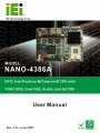
1
NANO-4386A Motherboard
Page i
NANO-4386A Motherboard
Revision
MODEL
NANO-4386A Motherboard
Revision Number
Description
Date of Issue
1.01
Updated Dimension Drawings
June 2007
1.00
Initial release
April 2007
Page ii
NANO-4386A Motherboard
Copyright
COPYRIGHT NOTICE
The information in this document is subject to change without prior notice in order to
improve reliability, design and function and does not represent a commitment on the part
of the manufacturer.
In no event will the manufacturer be liable for direct, indirect, special, incidental, or
consequential damages arising out of the use or inability to use the product or
documentation, even if advised of the possibility of such damages.
This document contains proprietary information protected by copyright. All rights are
reserved. No part of this manual may be reproduced by any mechanical, electronic, or
other means in any form without prior written permission of the manufacturer.
TRADEMARKS
IBM PC is a registered trademark of International Business Machines Corporation. INTEL
is a registered trademark of INTEL Corporation. Other product names mentioned herein
are used for identification purposes only and may be trademarks and/or registered
trademarks of their respective owners.
Page iii
NANO-4386A Motherboard
Packing List
NOTE:
If any of the components listed in the checklist below are missing, please do not
proceed with the installation. Contact the IEI reseller or vendor you purchased the
NANO-4386A motherboard from or contact an IEI sales representative directly. To
contact an IEI sales representative, please send an email to [email protected].
The items listed below should all be included in the NANO-4386A motherboard package.
1 x NANO-4386A Single Board Computer
1 x Mini Jumper Pack (P/N: 33100-000079-RS)
1 x IDE flat cable 44p/44p (P/N: 32200-000009-RS)
1 x Audio Cable (P/N: 32000-000147-RS)
1 x 4 RS-232 Adapter cable (P/N: 32200-025401-RS)
1 x Power cable (P/N: 32100-087100-RS)
1 x Utility CD (P/N: IEI-7B000-000104-RS)
1 x QIG (Quick Installation Guide)
Images of the above items are shown in Chapter 3.
Page iv
NANO-4386A Motherboard
Table of Contents
1
INTRODUCTION..................................................................................................... 1
1.1 NANO-4386A OVERVIEW ......................................................................................... 2
1.1.1 NANO-4386A Features ...................................................................................... 2
1.2 NANO-4386A OVERVIEW ......................................................................................... 3
1.2.1 NANO-4386A Overview Photo .......................................................................... 3
1.2.2 NANO-4386A Peripheral Connectors and Jumpers.......................................... 4
1.2.3 Technical Specifications..................................................................................... 5
2
DETAILED SPECIFICATIONS ............................................................................. 7
2.1 OVERVIEW ................................................................................................................. 8
2.2 DIMENSIONS .............................................................................................................. 8
2.2.1 Board Dimensions.............................................................................................. 8
2.2.2 External Interface Panel Dimensions ................................................................ 9
2.3 DATA FLOW .............................................................................................................. 10
2.4 COMPATIBLE PROCESSORS ........................................................................................11
2.4.1 CPU Overview ..................................................................................................11
2.4.2 Supported Intel® Pentium® M Processors ......................................................11
2.4.3 Supported Intel® Celeron® M Processors .......................................................11
2.5 INTEL® 852GM NORTHBRIDGE CHIPSET...................................................................11
2.5.1 Intel® 852GM Overview....................................................................................11
2.5.2 Intel® 852GM Memory Support ...................................................................... 12
2.5.3 Intel® 852GM Integrated Graphics Controller............................................... 13
2.6 INTEL® ICH4 SOUTHBRIDGE CHIPSET ..................................................................... 14
2.6.1 Intel® ICH4 Overview ...................................................................................... 14
2.6.2 Intel® ICH4 Audio Codec ’97 Controller......................................................... 14
2.6.3 Intel® ICH4 IDE Interface ............................................................................... 15
2.6.4 Intel® ICH4 Low Pin Count (LPC) Interface................................................... 15
2.6.5 Intel® ICH4 PCI Interface ............................................................................... 16
2.6.6 Intel® ICH4 Real Time Clock ........................................................................... 16
2.6.7 Intel® ICH4 USB Controller ............................................................................ 16
2.7 PCI BUS ................................................................................................................... 16
Page v
NANO-4386A Motherboard
2.8 LPC BUS COMPONENTS ........................................................................................... 16
2.8.1 LPC Bus Overview........................................................................................... 16
2.8.2 BIOS Chipset.................................................................................................... 16
2.8.3 Super I/O chipset.............................................................................................. 17
2.8.3.1 Super I/O LPC Interface ........................................................................... 17
2.8.3.2 Super I/O 16C550 UARTs ........................................................................ 18
2.8.3.3 Super I/O Hardware Monitor .................................................................... 18
2.8.3.4 Super I/O Parallel Port .............................................................................. 19
2.8.3.5 Super I/O Keyboard Controller................................................................. 19
2.8.3.6 Super I/O Infrared (IrDA)......................................................................... 20
2.8.3.7 Super I/O General Purpose I/O (GPIO) Ports........................................... 20
2.9 ENVIRONMENTAL AND POWER SPECIFICATIONS ....................................................... 20
2.9.1 System Monitoring ........................................................................................... 20
2.9.2 Operating Temperature and Temperature Control........................................... 21
2.9.3 Power Consumption......................................................................................... 21
3
UNPACKING .......................................................................................................... 23
3.1 ANTI-STATIC PRECAUTIONS ...................................................................................... 24
3.2 UNPACKING.............................................................................................................. 25
3.2.1 Unpacking Precautions.................................................................................... 25
3.3 UNPACKING CHECKLIST ........................................................................................... 25
3.3.1 Package Contents............................................................................................. 25
3.3.2 Optional Components ...................................................................................... 26
4
CONNECTOR PINOUTS...................................................................................... 29
4.1 PERIPHERAL INTERFACE CONNECTORS .................................................................... 30
4.1.1 NANO-4386A Layout ....................................................................................... 30
4.1.2 Peripheral Interface Connectors ..................................................................... 31
4.1.3 External Peripheral Interface Panel Connectors ............................................ 32
4.2 INTERNAL PERIPHERAL CONNECTORS ...................................................................... 33
4.2.1 +5VSB Connector (3-pins) .............................................................................. 33
4.2.2 12V Power Connector (4-pins) ........................................................................ 34
4.2.3 Audio Connector (10-pin) ................................................................................ 35
4.2.4 Battery Connector (2-pin)................................................................................ 36
4.2.5 Compact Flash Socket...................................................................................... 37
Page vi
NANO-4386A Motherboard
4.2.6 Digital Input/Output (DIO) Connector............................................................ 39
4.2.7 Fan Connector ................................................................................................. 40
4.2.8 Front Panel Connector .................................................................................... 41
4.2.9 IDE Connector (44-pin)................................................................................... 42
4.2.10 Infrared Interface Connector (5-pin) ............................................................. 44
4.2.11 Inverter Connector ......................................................................................... 45
4.2.12 LVDS Connector ............................................................................................ 46
4.2.13 PC/104 Connector ......................................................................................... 48
4.2.14 PCI-104 Connector........................................................................................ 51
4.2.15 Power On Connector ..................................................................................... 54
4.2.16 Serial Port Connector (RS-232)..................................................................... 55
4.2.17 Serial Port Connector (RS-232/422/485) ...................................................... 57
4.2.18 SO-DIMM Socket ........................................................................................... 59
4.2.19 USB Connectors (Internal) ............................................................................ 62
4.3 EXTERNAL PERIPHERAL INTERFACE CONNECTORS .................................................. 63
4.3.1 VGA Connector ................................................................................................ 64
4.3.2 Serial Communications Connector .................................................................. 65
4.3.3 Ethernet Connector.......................................................................................... 66
4.3.4 USB Connectors............................................................................................... 67
4.3.5 Keyboard/Mouse Connector ............................................................................ 68
4.4 ON-BOARD JUMPERS ................................................................................................ 68
5
INSTALLATION .................................................................................................... 69
5.1 ANTI-STATIC PRECAUTIONS ...................................................................................... 70
5.2 INSTALLATION CONSIDERATIONS ............................................................................. 71
5.2.1 Installation Notices .......................................................................................... 71
5.2.2 Installation Checklist ....................................................................................... 72
5.3 CPU, CPU COOLING KIT AND DIMM INSTALLATION ............................................. 73
5.3.1 Socket 479 CPU Installation............................................................................ 73
5.3.2 Cooling Kit CF-479B-RS Installation.............................................................. 76
5.3.3 SO-DIMM Installation ..................................................................................... 78
5.3.4 CF Card Installation........................................................................................ 79
5.4 JUMPER SETTINGS .................................................................................................... 80
5.4.1 CF Card Setup ................................................................................................. 82
5.4.2 Clear CMOS Jumper........................................................................................ 82
Page vii
NANO-4386A Motherboard
5.4.3 COM2 RS-232/422/485 Setup Jumper............................................................. 83
5.4.4 LCD Voltage Setup ........................................................................................... 84
5.4.5 PCI-104 Voltage Setup ..................................................................................... 84
5.5 CHASSIS INSTALLATION ........................................................................................... 85
5.5.1 Airflow.............................................................................................................. 85
5.6 INTERNAL PERIPHERAL DEVICE CONNECTIONS........................................................ 85
5.6.1 Peripheral Device Cables ................................................................................ 85
5.6.2 ATA Flat Cable Connection ............................................................................. 86
5.6.3 AT Power Connection ...................................................................................... 87
5.6.4 ATX Power Connection.................................................................................... 89
5.6.5 Audio Kit Installation....................................................................................... 93
5.6.6 Serial Port Connector Cable (Four Ports) Cable Connection ........................ 94
5.7 EXTERNAL PERIPHERAL INTERFACE CONNECTION ................................................... 95
5.7.1 PS/2 Keyboard/Mouse Connection .................................................................. 95
5.7.2 RJ-45 Ethernet Connection.............................................................................. 96
5.7.3 USB Connection (Dual Connector) ................................................................. 97
5.7.4 VGA Monitor Connection ................................................................................ 98
5.7.5 Serial Device Connection ................................................................................ 99
6
AMI BIOS.............................................................................................................. 101
6.1 INTRODUCTION ...................................................................................................... 102
6.1.1 Starting Setup................................................................................................. 102
6.1.2 Using Setup .................................................................................................... 102
6.1.3 Getting Help................................................................................................... 103
6.1.4 Unable to Reboot After Configuration Changes............................................ 103
6.1.5 BIOS Menu Bar.............................................................................................. 103
6.2 MAIN ..................................................................................................................... 104
6.3 ADVANCED ............................................................................................................. 106
6.3.1 CPU Configuration........................................................................................ 107
6.3.2 IDE Configuration ......................................................................................... 109
6.3.2.1 IDE Master, IDE Slave ............................................................................111
6.3.3 IO Configuration.............................................................................................116
6.3.4 Hardware Health Configuration.....................................................................118
6.3.5 USB Configuration......................................................................................... 120
6.3.5.1 USB Mass Storage Device Configuration............................................... 123
Page viii
NANO-4386A Motherboard
6.4 PCI/PNP ................................................................................................................ 125
6.5 BOOT ..................................................................................................................... 130
6.5.1 Boot Settings Configuration........................................................................... 131
6.5.2 Boot Device Priority ...................................................................................... 132
6.5.3 Hard Disk Drives ........................................................................................... 133
6.5.4 Removable Drives .......................................................................................... 134
6.5.5 CD/DVD Drives ............................................................................................. 135
6.6 SECURITY............................................................................................................... 136
6.7 CHIPSET ................................................................................................................. 138
6.7.1 NorthBridge Configuration............................................................................ 139
6.7.1.1 Video Function Configuration ................................................................ 143
6.7.2 SouthBridge Configuration............................................................................ 145
6.8 POWER ................................................................................................................... 146
6.9 EXIT ....................................................................................................................... 149
7
DRIVER INSTALLATION.................................................................................. 151
7.1 AVAILABLE SOFTWARE DRIVERS ............................................................................ 152
7.2 DRIVER CD AUTO-RUN .......................................................................................... 152
7.3 CHIPSET DRIVER INSTALLATION............................................................................. 154
7.4 INTEL GRAPHICS MEDIA ACCELERATOR DRIVER ................................................... 157
7.5 INTEL® NETWORK ADAPTER INSTALLATION ......................................................... 161
7.6 INTEL® USB 2.0 INSTALLATION............................................................................ 166
7.7 REALTEK AC`97 AUDIO DRIVER (ALC665) INSTALLATION .................................. 171
7.7.1 BIOS Setup ..................................................................................................... 171
7.7.2 Driver Installation ......................................................................................... 171
A
BIOS MENU OPTIONS....................................................................................... 177
A.1 BIOS CONFIGURATION OPTIONS........................................................................... 178
B
WATCHDOG TIMER .......................................................................................... 181
C
ADDRESS MAPPING.......................................................................................... 185
C.1 IO ADDRESS MAP ................................................................................................. 186
C.2 1ST MB MEMORY ADDRESS MAP ......................................................................... 186
C.3 IRQ MAPPING TABLE ............................................................................................ 187
C.4 DMA CHANNEL ASSIGNMENTS ............................................................................. 187
Page ix
NANO-4386A Motherboard
D
EXTERNAL AC’97 AUDIO CODEC ................................................................. 189
D.1 INTRODUCTION ..................................................................................................... 190
D.1.1 Accessing the AC’97 CODEC ....................................................................... 190
D.1.2 Driver Installation......................................................................................... 190
D.2 SOUND EFFECT CONFIGURATION........................................................................... 191
D.2.1 Accessing the Sound Effects Manager .......................................................... 191
D.2.2 Sound Effect Manager Configuration Options ............................................. 192
INDEX............................................................................................................................ 195
Page x
NANO-4386A Motherboard
List of Figures
Figure 1-1: NANO-4386A Overview - Front.................................................................3
Figure 1-2: NANO-4386A Overview - Back .................................................................4
Figure 2-1: NANO-4386A Dimensions (mm) ...............................................................8
Figure 2-2: External Interface Panel Dimensions (mm).............................................9
Figure 2-3: Data Flow Block Diagram........................................................................10
Figure 2-4: 200-pin SO-DIMM Socket ........................................................................12
Figure 4-1: Connector and Jumper Locations - Front.............................................30
Figure 4-2: Connector and Jumper Locations - Back .............................................31
Figure 4-3: +5VSB Connector Location ....................................................................33
Figure 4-4: 12V Power Connector (4-pins) Location ...............................................34
Figure 4-5: Audio Connector Location (8-pin) .........................................................35
Figure 4-6: Battery Connector Location (2-pin) .......................................................36
Figure 4-7: CF Card Socket Location ........................................................................38
Figure 4-8: DIO Connector Locations .......................................................................40
Figure 4-9: Fan Connector Location .........................................................................41
Figure 4-10: Front Panel Connector Pinout Locations............................................42
Figure 4-11: IDE Device Connector Locations .........................................................43
Figure 4-12: Infrared Connector Pinout Locations ..................................................45
Figure 4-13: Inverter Connector Location ................................................................46
Figure 4-14: LVDS Connector Location ....................................................................47
Figure 4-15: PC/104 Connector Pinout Locations ...................................................49
Figure 4-16: PCI-104 Connector Location ................................................................52
Figure 4-17: Power On Connector Location.............................................................54
Figure 4-18: Serial Port Connector (RS-232) Pinout Locations..............................56
Figure 4-19: Serial Port Connector (RS-232/422/485) Pinout Locations................58
Figure 4-20: SO-DIMM Socket Location ....................................................................60
Figure 4-21: USB Connector Pinout Locations........................................................63
Figure 4-22: NANO-4386A External Peripheral Connector Panel...........................64
Page xi
NANO-4386A Motherboard
Figure 4-23: VGA Connector ......................................................................................64
Figure 4-24: Serial Communications Connector Pinout Locations .......................65
Figure 4-25: Ethernet Connector ...............................................................................66
Figure 4-26: PS/2 Pinout and Configuration.............................................................68
Figure 5-1: Make sure the CPU socket retention screw is unlocked .....................74
Figure 5-2: Lock the CPU Socket Retention Screw .................................................75
Figure 5-3: IEI CF-479B-RS Cooling Kit ....................................................................76
Figure 5-4: Cooling Kit Support Bracket...................................................................77
Figure 5-5: Connect the cooling fan cable ...............................................................77
Figure 5-6: SO-DIMM Installation...............................................................................78
Figure 5-7: CF Card Installation.................................................................................80
Figure 5-8: Jumpers ....................................................................................................80
Figure 5-9: Jumper Locations....................................................................................81
Figure 5-10: IDE Cable Connection ...........................................................................87
Figure 5-11: Power Cable to Motherboard Connection...........................................88
Figure 5-12: Connect Power Cable to Power Supply ..............................................89
Figure 5-13: Power Cable to Motherboard Connection...........................................90
Figure 5-14: Connect Power Cable to ATX Adapter Cable......................................91
Figure 5-15: Connect ATX Power Adapter Cable to Power Supply .......................92
Figure 5-16: Connect ATX Power Cable to Motherboard ........................................92
Figure 5-17: Audio Kit Cable Connection .................................................................93
Figure 5-18: Four Serial Port Connector Cable Connection ...................................94
Figure 5-19: PS/2 Connector ......................................................................................96
Figure 5-20: RJ-45 Ethernet Connector ....................................................................97
Figure 5-21: USB Connector ......................................................................................98
Figure 5-22: VGA Connector ......................................................................................99
Figure 5-23: Serial Device Connector .................................................................... 100
Figure 7-1: Introduction Screen.............................................................................. 153
Figure 7-2: Available Drivers................................................................................... 153
Figure 7-3: Chipset Driver Installation Program ................................................... 154
Figure 7-4: Chipset Driver Installation Welcome Screen ..................................... 155
Figure 7-5: Chipset Driver Installation License Agreement................................. 155
Page xii
NANO-4386A Motherboard
Figure 7-6: Chipset Driver Readme File Information ............................................ 156
Figure 7-7: Chipset Driver Installation Complete.................................................. 156
Figure 7-8: Select the Operating System ............................................................... 157
Figure 7-9: VGA Driver............................................................................................. 158
Figure 7-10: Intel® Graphics Media Accelerator InstallShield Wizard................ 158
Figure 7-11: InstallShield Wizard Extracting Files................................................ 159
Figure 7-12: Intel® Graphics Media Accelerator Driver Welcome Screen ......... 159
Figure 7-13: Intel® Graphics Media Accelerator Driver License Agreement ..... 160
Figure 7-14: Intel® Graphics Media Accelerator Driver Installing Notice........... 160
Figure 7-15: Intel® Graphics Media Accelerator Installation Complete ............. 161
Figure 7-16: Select the Driver Folder ..................................................................... 162
Figure 7-17: Select the Driver ................................................................................. 162
Figure 7-18: Network Adapter License Agreement............................................... 163
Figure 7-19: Location to Save Files........................................................................ 163
Figure 7-20: InstallShield Wizard Extracting Files................................................ 164
Figure 7-21: Overwrite Protection .......................................................................... 164
Figure 7-22: File Extraction Continues .................................................................. 165
Figure 7-23: Intel® Pro Network Connections....................................................... 165
Figure 7-24: Intel® Pro Network Connections Driver Installation Notice ........... 166
Figure 7-25: USB2.0 Window .................................................................................. 166
Figure 7-26: USB2.0 OS Options ............................................................................ 167
Figure 7-27: Windows XP USB 2.0 Program Icon ................................................. 167
Figure 7-28: USB 2.0 InstallShield Wizard ............................................................. 168
Figure 7-29: USB 2.0 InstallShield Wizard Continues .......................................... 168
Figure 7-30: USB 2.0 InstallShield Wizard Welcome Screen ............................... 169
Figure 7-31: USB 2.0 License Agreement.............................................................. 169
Figure 7-32: USB 2.0 Driver Installed ..................................................................... 170
Figure 7-33: USB 2.0 Driver Installation Complete ............................................... 170
Figure 7-34: Select the Audio CODEC.................................................................... 172
Figure 7-35: Locate the Setup Program Icon ........................................................ 173
Figure 7-36: Preparing Setup Screen ..................................................................... 173
Figure 7-37: InstallShield Wizard Welcome Screen.............................................. 174
Page xiii
NANO-4386A Motherboard
Figure 7-38: Audio Driver Software Configuration ............................................... 174
Figure 7-39: Audio Driver Digital Signal ................................................................ 175
Figure 7-40: Audio Driver Installation .................................................................... 175
Figure 7-41: Restart the Computer ......................................................................... 176
Page xiv
NANO-4386A Motherboard
List of Tables
Table 1-1: Technical Specifications ............................................................................6
Table 2-1: Supported Intel® Pentium® M Processors.............................................11
Table 2-2: Supported Intel® Celeron® M Processors................................................11
Table 2-3: Supported HDD Specifications ................................................................15
Table 2-4: Power Consumption .................................................................................21
Table 3-1: Package List Contents..............................................................................26
Table 3-2: Optional Components...............................................................................27
Table 4-1: Peripheral Interface Connectors..............................................................32
Table 4-2: External Peripheral Interface Panel Connectors....................................32
Table 4-3: +5VSB Connector Pinouts........................................................................34
Table 4-4: 12V Power Connector (4-pins) Pinouts...................................................35
Table 4-5: Audio Connector Pinouts (10-pin)...........................................................36
Table 4-6: Battery Connector Pinouts (2-pin)...........................................................37
Table 4-7: CF Card Socket Pinouts ...........................................................................39
Table 4-8: DIO Connector Pinouts.............................................................................40
Table 4-9: Fan Connector Pinouts.............................................................................41
Table 4-10: Front Panel Connector Pinouts .............................................................42
Table 4-11: IDE Connector Pinouts ...........................................................................44
Table 4-12: Infrared Connector Pinouts....................................................................45
Table 4-13: Inverter Connector Pinouts ....................................................................46
Table 4-14: LVDS Connector Pinouts........................................................................48
Table 4-15: PC/104 Connector Pinouts .....................................................................50
Table 4-16: PCI-104 Connector Pinouts ....................................................................53
Table 4-17: Power On Connector Pinouts ................................................................54
Table 4-18: Serial Port Connector (RS-232) Pinouts ...............................................57
Table 4-19: Serial Port Connector (RS-232/422/485) Pinouts .................................58
Table 4-20: SO-DIMM Socket Pinouts .......................................................................62
Table 4-21: USB Port Connector Pinouts .................................................................63
Page xv
NANO-4386A Motherboard
Table 4-22: VGA Connector Pinouts .........................................................................64
Table 4-23: COM1 RS-232 Mode Connector Pinouts ...............................................65
Table 4-24: Ethernet Connector Pinouts...................................................................66
Table 4-25: Ethernet Connector LEDs.......................................................................67
Table 4-26: USB Connector Pinouts..........................................................................67
Table 4-27: Keyboard Connector Pinouts ................................................................68
Table 5-1: Jumpers ....................................................................................................81
Table 5-2: CF Card Setup Jumper Settings ..............................................................82
Table 5-3: Clear CMOS Jumper Settings ..................................................................83
Table 5-4: COM2 RS-232/422/485 Setup Jumper Settings ......................................83
Table 5-5: LCD Voltage Setup Jumper Settings.......................................................84
Table 5-6: PCI-104 Voltage Setup Jumper Settings.................................................85
Table 5-7: IEI Provided Cables...................................................................................86
Table 6-1: BIOS Navigation Keys............................................................................ 103
Page xvi
NANO-4386A Motherboard
List of BIOS Menus
BIOS Menu 1: Main ................................................................................................. 104
BIOS Menu 2: Advanced.......................................................................................... 106
BIOS Menu 3: CPU Configuration........................................................................... 107
BIOS Menu 4: IDE Configuration ............................................................................ 109
BIOS Menu 5: IDE Master and IDE Slave Configuration....................................... 111
BIOS Menu 6: Super IO Configuration ................................................................... 116
BIOS Menu 7: Hardware Health Configuration...................................................... 118
BIOS Menu 8: USB Configuration........................................................................... 120
BIOS Menu 9: USB Mass Storage Device Configuration...................................... 123
BIOS Menu 10: PCI/PnP Configuration .................................................................. 125
BIOS Menu 11: Boot................................................................................................. 130
BIOS Menu 12: Boot Settings Configuration......................................................... 131
BIOS Menu 13: Boot Device Priority Settings ....................................................... 133
BIOS Menu 14: Hard Disk Drives ............................................................................ 134
BIOS Menu 15: Removable Drives.......................................................................... 135
BIOS Menu 16: CD/DVD Drives ............................................................................... 136
BIOS Menu 17: Security........................................................................................... 136
BIOS Menu 18: Chipset............................................................................................ 138
BIOS Menu 19:NorthBridge Chipset Configuration.............................................. 139
BIOS Menu 20:SouthBridge Chipset Configuration ............................................. 145
BIOS Menu 21: Power .............................................................................................. 146
BIOS Menu 22:Exit ................................................................................................. 149
Page xvii
NANO-4386A Motherboard
Glossary
AC’97
Audio Codec 97
HDD
Hard Disk Drive
ACPI
Advanced Configuration and
IDE
Integrated Data Electronics
Power Interface
I/O
Input/Output
APM
Advanced Power Management
ICH4
I/O Controller Hub 4
ARMD
ATAPI Removable Media Device
L1 Cache Level 1 Cache
ASKIR
Shift Keyed Infrared
L2 Cache Level 2 Cache
ATA
Advanced Technology
LCD
Liquid Crystal Display
Attachments
LPT
Parallel Port Connector
BIOS
Basic Input/Output System
LVDS
Low Voltage Differential Signaling
CFII
Compact Flash Type 2
MAC
Media Access Controller
CMOS
Complementary Metal Oxide
OS
Operating System
Semiconductor
PCI
Peripheral Connect Interface
CPU
Central Processing Unit
PIO
Programmed Input Output
Codec
Compressor/Decompressor
PnP
Plug and Play
COM
Serial Port
POST
Power On Self Test
DAC
Digital to Analog Converter
RAM
Random Access Memory
DDR
Double Data Rate
SATA
Serial ATA
DIMM
Dual Inline Memory Module
S.M.A.R.T Self Monitoring Analysis and
DIO
Digital Input/Output
DMA
Direct Memory Access
SPD
Serial Presence Detect
EIDE
Enhanced IDE
S/PDI
Sony/Philips Digital Interface
EIST
Enhanced Intel SpeedStep
SDRAM
Synchronous Dynamic Random
Reporting Technology
Access Memory
Technology
FDD
Floppy Disk Drive
SIR
Serial Infrared
FDC
Floppy Disk Connector
UART
Universal Asynchronous
FFIO
Flexible File Input/Output
FIFO
First In/First Out
USB
Universal Serial Bus
FSB
Front Side Bus
VGA
Video Graphics Adapter
IrDA
Infrared Data Association
Page xviii
Receiver-transmitter
NANO-4386A Motherboard
Chapter
1
1 Introduction
Page 1
NANO-4386A Motherboard
1.1 NANO-4386A Overview
The NANO-4386A motherboard is an Intel® Pentium® M/Celeron® M CPU platform with an
Intel® 852GM Chipset and Intel® I/O Controller Hub 4 (ICH4) Southbridge. The
NANO-4386A has a maximum front side bus (FSB) frequency of 400MHz, supports up to
1GB of dual channel 266MHz DDR SO-DIMM RAM and comes with VGA, LVDS, PS/2
keyboard/mouse and COM port interfaces as well as a dual Intel® 82551ER or 82541P1
(GbE) chipsets. The NANO-4386A supports up to two IDE hard disk drives, six USB 2.0
devices, Infrared Data Association (IrDA) communications and expansion is via a
PC/104-Plus interface. If RAID support for the system is required, please contact an IEI
sales representative, or send an email to [email protected].
1.1.1 NANO-4386A Features
Some of the NANO-4386A features are listed below.
EPIC form factor
RoHS compliant
Support for the following CPUs:
o
o
Socket 479 Intel® Pentium® M
Socket 479 Intel® Celeron® M
Maximum FSB of 400MHz
A 200-pin single channel 266MHz DDR SO-DIMM supports up to 1GB of
memory
Dual Intel® 82551ER Ethernet/Dual Intel® 82541PI GbE chipsets
Realtek ALC655 – AC’97 audio
Two Ultra ATA 100, Ultra ATA 66 or Ultra ATA 33 IDE HDDs supported
Six USB 2.0 devices supported
Six COM ports supported
LVDS supported
Page 2
NANO-4386A Motherboard
1.2 NANO-4386A Overview
1.2.1 NANO-4386A Overview Photo
The NANO-4386A has a wide variety of internal and external peripheral connectors. The
peripheral connectors are connected to devices including storage devices, display devices
and communications devices. A labeled photo of the peripheral connectors on the front
side of the motherboard is shown in Figure 1-1.
Figure 1-1: NANO-4386A Overview - Front
Page 3
NANO-4386A Motherboard
A labeled photo of the peripheral connectors on the front side of the motherboard is shown
in Figure 1-2.
Figure 1-2: NANO-4386A Overview - Back
1.2.2 NANO-4386A Peripheral Connectors and Jumpers
The NANO-4386A has the following on-board connectors:
1 x 12V power connector
1 x ATX power connector
1 x Audio connector
1 x Battery connector
1 x CompactFlash socket
1 x DDR SO-DIMM socket
1 x DIO connector
1 x Fan connector
1 x Front panel connector
1 x IDE disk drive connector
1 x Infrared interface connector
1 x Inverter connector
1 x LVDS connector
1 x PC/104 connector
1 x PCI-104 connector
Page 4
NANO-4386A Motherboard
6 x Serial port connectors
6 x USB connectors
The NANO-4386A has the following external peripheral interface connectors on the board
rear panel:
1 x PS/2 dual keyboard/mouse connector
1 x Serial port connector
1 x VGA connector
2 x Ethernet connectors
2 x USB connectors
The NANO-4386A has the following on-board jumpers:
CF Master/Slave Setup
Clear CMOS
COM2 RS-232/422/485 Setup
LCD Voltage Setup
PCI-104 Voltage Setup
1.2.3 Technical Specifications
NANO-4386A technical specifications are listed in Table 1-1. Detailed descriptions of
each specification can be found in Chapter 2.
Specification
NANO-4386A
Form Factor
EPIC
Socket 479 Intel® Pentium® M (up to 2.10GHz)
System CPU
Socket 479 Intel® Celeron® M (up to 1.40GHz)
Front Side Bus
400MHz
Northbridge: Intel® 852GM
System Chipset
Southbridge: Intel® ICH4
Memory
One 200-pin single channel DDR 266MHz SO-DIMM up to1GB
Display
- VGA Integrated in Intel® 852GM
Page 5
NANO-4386A Motherboard
Specification
NANO-4386A
- 18-bit dual channel LVDS
BIOS
AMI BIOS
Audio
Realtek ALC655 AC'97 codec
- Dual Intel® 82551ER Ethernet chipsets
LAN
- Dual Intel® 82541PI GbE chipsets
Six on-board serial ports:
COM
Five on-board RS-232 serial ports
One on-board RS-232/422/485 serial port (by jumper setting)
USB 2.0
Six USB 2.0 devices supported
IDE
One 44-pin IDE connects up to two Ultra ATA33/66/100 devices
Keyboard/mouse
One PS/2 connector supports mouse and keyboard connectivity
Watchdog Timer
Software programmable 1-255 sec. by super I/O
[email protected], 5VSB@ 0.22A
Power Supply
(Intel® Celeron® M 1.4GHz CPU with 512MB DDR 266MHz)
Temperature
0ºC ~ 60ºC (32ºF~140ºF)
Humidity (operating)
5%~95% non-condensing
Dimensions
165mm x 115mm
Weight (GW/NW)
800g/233kg
Table 1-1: Technical Specifications
Page 6
NANO-4386A Motherboard
Chapter
2
2 Detailed Specifications
Page 7
NANO-4386A Motherboard
2.1 Overview
This chapter describes the specifications and on-board features of the NANO-4386A in
detail.
2.2 Dimensions
2.2.1 Board Dimensions
The dimensions of the board are listed below and shown in Figure 2-1.
Length:
165 mm
Width:
115 mm
Figure 2-1: NANO-4386A Dimensions (mm)
Page 8
NANO-4386A Motherboard
2.2.2 External Interface Panel Dimensions
External peripheral interface connector panel dimensions are shown in Figure 2-2.
Figure 2-2: External Interface Panel Dimensions (mm)
Page 9
NANO-4386A Motherboard
2.3 Data Flow
Figure 2-3 shows the data flow between the two on-board chipsets and other components
installed on the motherboard and described in the following sections of this chapter.
Figure 2-3: Data Flow Block Diagram
Page 10
NANO-4386A Motherboard
2.4 Compatible Processors
2.4.1 CPU Overview
Socket 479 Intel® Pentium® M and Intel® Celeron® M processors can be installed on the
NANO-4386A motherboard.
2.4.2 Supported Intel® Pentium® M Processors
Specifications for the compatible Intel® Pentium® M processors are listed in Table 2-1.
CPU Speed
Bus Speed
Mfg. Tech
Cache
Package
Processor No.
2.10GHz
400 MHz
90 nm
2 MB
Socket 479
-
1.60 GHz
400 MHz
90 nm
2 MB
Socket 479
778
1.40 GHz
400 MHz
90 nm
2 MB
Socket 479
-
Table 2-1: Supported Intel® Pentium® M Processors
2.4.3 Supported Intel® Celeron® M Processors
Specifications for the compatible Intel® Celeron® M processors are listed in Table 2-2.
CPU Speed
Bus Speed
Mfg. Tech
Cache
Package
Processor No.
1.40 GHz
400 MHz
90 nm
1 MB
Socket 479
360
1.30 GHz
400 MHz
90 nm
1 MB
Socket 479
350
900 MHz
400 MHz
90 nm
512 KB Socket 479
353
Table 2-2: Supported Intel® Celeron® M Processors
2.5 Intel® 852GM Northbridge Chipset
2.5.1 Intel® 852GM Overview
The Intel 852GM GMCH is a graphics memory controller hub (GMCH) component for
mobile platforms. It provides the processor interface, system memory interface
Page 11
NANO-4386A Motherboard
(DDR-SDRAM), Hub interface, CRT, LVDS, and one DVO port. An ACPI-compliant Intel
852GM chipset platform can support the Full-On (S0), Power On Suspend (S1-M),
Suspend to RAM (S3), Suspend to Disk (S4), and Soft-Off (S5) power management
states. Through the use of an appropriate LAN device, the chipset also supports wake-on
LAN for remote administration and troubleshooting. The Intel 852GM GMCH integrates
the following:
400-MHz processor Front Side Bus (FSB) controller
Graphics controller interface
Dual Channel 18 bit LVDS interface for TFT panel support
One Digital Video Out Port (DVO)
Supports DDR200/266 MHz memory technology
High-speed Accelerated Hub Architecture interface for communication with
the ICH4-M
2.5.2 Intel® 852GM Memory Support
The Intel® 852GM supports one, 1GB, 266MHz single channel DDR SO-DIMM. The
memory socket is shown in Figure 2-4.
Figure 2-4: 200-pin SO-DIMM Socket
Page 12
NANO-4386A Motherboard
2.5.3 Intel® 852GM Integrated Graphics Controller
The Intel® 852GM has a graphics controller integrated into the chipset. Some of the
features of the Intel® 852GM Integrated Graphics Controller are listed below.
Graphics Core Frequency of 133 MHz
3D Graphics Engine
o
o
3D Setup and Render Engine
High quality performance Texture Engine
Analog Display Support
o
o
o
350-MHz integrated 24-bit RAMDAC
Hardware color cursor support
Accompanying I2C and DDC channels provided through multiplexed
interface
o
o
Hotplug and display support
Dual independent pipe for dual independent display
Digital Video Out Port (DVO) support
o
Single channel DVO Port with 165-MHz dot clock support for a 12-bit
interface
o
Compliant with DVI Specification 1.0
Dedicated LFP (local flat panel) interface
o
Single or dual channel LVDS TFT panel support up to SXGA+ panel
resolution with frequency range from 25 MHz to 112 MHz per channel
o
SSC support of 0.5%, 1.0%, and 2.5% center and down spread with
external SSC clock
o
Dual Display Twin (Single pipe LVDS+CRT) is not supported if SSC is
enabled
o
o
o
o
o
Supports data format of 18 bpp
LCD panel power sequencing compliant with SPWG timing specification
Compliant with ANSI/TIA/EIA –644-1995 spec
Integrated PWM interface for LCD backlight inverter control
Compliant with CPIS Specification 1.5
Page 13
NANO-4386A Motherboard
2.6 Intel® ICH4 Southbridge Chipset
2.6.1 Intel® ICH4 Overview
The ICH4 southbridge chipset features are listed below.
PCI Bus Interface supports PCI Revision 2.2 Specification at 33 MHz and 133
MB/sec maximum throughput
Integrated LAN Controller with 10/100 Mbit/sec Ethernet support
Integrated IDE Controller supports Ultra ATA/100/66/33, BMIDE and PIO
modes
USB includes one EHCI high-speed USB 2.0 Host Controller and supports
legacy keyboard/mouse software
AC-Link for Audio supports AC ’97 2.3
Interrupt Controller
1.5 V operation with 3.3 V I/O
Timers Based on 82C54
Power Management Logic is ACPI 2.0 compliant
Enhanced Hub Interface
Firmware Hub (FWH) Interface supports BIOS memory size up to 8 MB
Low Pin Count (LPC) Interface supports two Master/DMA devices
Enhanced DMA Controller
Real-Time Clock 256-byte battery-backed CMOS RAM
Supports SMBus 2.0 Specification
GPIO
2.6.2 Intel® ICH4 Audio Codec ’97 Controller
The Audio Codec ’97 (AC’97) controller integrated into the ICH4 complies with AC’97
Component Specification, Version 2.3. The AC’97 controller is connected to the onboard
audio connector. The audio connector is connected to an optional 5.1 channel or 7.1
channel audio kit with an embedded AC’97 audio codec. The AC’97 controller supports up
to six PCM audio output channels. Complete surround sound requires six-channel audio
consisting of:
Front left
Page 14
NANO-4386A Motherboard
Front right
Back left
Back right
Center
Subwoofer
2.6.3 Intel® ICH4 IDE Interface
The integrated IDE interface on the ICH4 southbridge supports two IDE hard disks and
ATAPI devices, PIO IDE transfers up to 16MB/s and Ultra ATA transfers of 100MB/s. The
integrated IDE interface is able to support the following IDE HDDs:
Ultra ATA/100, with data transfer rates up to 100MB/s
Ultra ATA/66, with data transfer rates up to 66MB/s
Ultra ATA/33, with data transfer rates up to 33MB/s
Table 2-3 shows the supported HDD specifications.
Specification
IDE devices
PIO Mode
PIO Max Transfer Rate
DMA/UDMA designation
DMA/UDMA Max Transfer
Controller Interface
Ultra ATA/100
Ultra ATA/66
Ultra ATA/33
2
2
2
0–4
0–4
0–4
16.6 MB/s
16.6 MB/s
16.6 MB/s
UDMA 3 - 4
UDMA 3 – 4
UDMA 2
100MB/s
66MB/s
33MB/s
5V
5V
5V
Table 2-3: Supported HDD Specifications
2.6.4 Intel® ICH4 Low Pin Count (LPC) Interface
The ICH4 LPC interface complies with the LPC 1.0 specifications. The LPC bus from the
ICH4 is connected to the following components:
BIOS chipset
Super I/O chipset
Page 15
NANO-4386A Motherboard
2.6.5 Intel® ICH4 PCI Interface
The ICH4 PCI interface provides a 33 MHz, Rev. 2.2 compliant implementation. All PCI
signals are 5 V tolerant, except PME#. The ICH4 integrates a PCI arbiter that supports up
to six external PCI bus masters in addition to the internal ICH4 requests.
2.6.6 Intel® ICH4 Real Time Clock
256 bytes of battery backed RAM is provided by the Motorola MC146818A real time clock
(RTC) integrated into the ICH4. The RTC operates on a 3V battery and 32.768KHz crystal.
The RTC keeps track of the time and stores system data even when the system is turned
off.
2.6.7 Intel® ICH4 USB Controller
Up to six high-speed, full-speed or low-speed USB devices are supported by the ICH4.
High-speed USB 2.0, with data transfers of up to 480Mb/s, is enabled with the ICH4
integrated Enhanced Host Controller Interface (EHCI) compliant host controller. USB
full-speed and low-speed signaling is supported by the four ICH4 integrated Universal
Host Controller Interface (UHCI) controller.
2.7 PCI Bus
The PCI bus controller on the ICH4 southbridge is compliant with PCI Revision 2.2
specifications and has a 33MHz PCI clock.
2.8 LPC Bus Components
2.8.1 LPC Bus Overview
The LPC bus is connected to components listed below:
BIOS chipset
Super I/O chipset
2.8.2 BIOS Chipset
Page 16
NANO-4386A Motherboard
The BIOS chipset has a licensed copy of AMI BIOS installed on the chipset. Some of the
BIOS features are listed below:
AMI Flash BIOS
SMIBIOS (DMI) compliant
Console redirection function support
PXE (Pre-boot Execution Environment) support
USB booting support
2.8.3 Super I/O chipset
The Winbond W83627UHG Super I/O chipset is connected to the ICH4 southbridge
through the LPC bus. The Winbond W83627UHG is an LPC interface-based Super I/O
device that comes with Environment Controller integration. Some of the features of the
Winbond W83627UHG chipset are listed below:
Meet LPC Spec. 1.01
Support LDRQ# (LPC DMA), SERIRQ (Serial IRQ)
Integrated hardware monitor functions
Compliant with Microsoft PC2000/PC2001 Hardware Design Guide
Support DPM (Device Power Management), ACPI
Programmable configuration settings
Single 24- or 48-MHz clock input
Some of the Super I/O features are described in more detail below.
2.8.3.1 Super I/O LPC Interface
The LPC interface on the Super I/O complies with the Intel® Low Pin Count Specification
Rev. 1.01. The LPC interface supports both LDRQ# and SERIRQ protocols as well as PCI
PME# interfaces.
Page 17
NANO-4386A Motherboard
2.8.3.2 Super I/O 16C550 UARTs
The onboard Super I/O UARTs has the following:
Six high-speed, 16550-compatible UARTs with 16-byte send/receive FIFOs
MIDI compatible
Fully programmable serial-interface characteristics:
o
o
o
5, 6, 7 or 8-bit characters
Even, odd or no parity bit generation/detection
1, 1.5 or 2 stop-bit generation
Internal diagnostic capabilities:
o
o
Loop-back controls for communications link fault isolation
Break, parity, overrun, framing error simulation
Programmable baud rate generator allows division of clock source by any
value from 1 to (216-1)
Maximum baud rate up to 921K bps for clock source is 14.769 MHz and 1.5M
bps for 24 MHz
2.8.3.3 Super I/O Hardware Monitor
The Super I/O Hardware Monitor hardware parameters are reported in the BIOS and can
be read from the BIOS Hardware Health Configuration menu. Features include:
Smart Fan control system, supporting Smart Fan™ I - “Thermal Cruise™” and
“Speed Cruise™” modes and Smart Fan™ III functions
Programmable critical temperature to speed fan fully while current
temperature exceeds this temperature during Thermal Cruise™mode
Two thermal inputs from optionally-remote thermistors or thermal diode output
Support current mode (dual current source) temperature measurement
method
Eight voltage inputs (CPUVCORE, VIN [0..2] and intrinsic 5VCC, AVCC ,
5VSB, VBAT)
Two fan-speed monitoring inputs
Two fan-speed controls
Dual mode for fan control (PWM and DC)
Built-in case open detection circuit
Page 18
NANO-4386A Motherboard
Programmable hysteresis and setting points for all monitored items
Over-temperature indicator output
Issue SMI#, OVT# to activate system protection
Winbond Hardware Doctor™ Support
Provide I2C interface to read / write registers
2.8.3.4 Super I/O Parallel Port
The Super I/O parallel port (LPT) features are listed below.
Compatible with IBM parallel port
Support PS/2-compatible bi-directional parallel port
Support Enhanced Parallel Port (EPP) - Compatible with IEEE 1284
specification
Support Extended Capabilities Port (ECP) - Compatible with IEEE 1284
specification
Enhanced printer port back-drive current protection
2.8.3.5 Super I/O Keyboard Controller
The Super I/O keyboard controller features are listed below.
8042-based keyboard controller
Support Phoenix MultiKey/42TM firmware
Asynchronous Access to two data registers and one status register
Software-compatible with 8042
Support PS/2 mouse
Support port 92
Support both interrupt and polling modes
Fast Gate A20 and Hardware Keyboard Reset
8-bit timer / counter
Support binary and BCD arithmetic
6, 8, 12, or 16 MHz operating frequency
Page 19
NANO-4386A Motherboard
2.8.3.6 Super I/O Infrared (IrDA)
The Super I/O infrared features are listed below.
Support IrDA version 1.0 SIR protocol with maximum baud rate up to 115.2K
bps
Support SHARP ASK-IR protocol with maximum baud rate up to 57,600 bps
2.8.3.7 Super I/O General Purpose I/O (GPIO) Ports
The Super I/O GPIO features are listed below.
45 programmable general purpose I/O ports
GP25, GP26 and GP27 can distinguish that input pins have any transitions by
reading registers and all of 3 GPIOs also can assert PSOUT# or PME# to
wake-up system if each them has any transition.
2.9 Environmental and Power Specifications
2.9.1 System Monitoring
Three thermal inputs on the NANO-4386A Super I/O Enhanced Hardware Monitor the
following temperatures:
System temperature
CPU temperature
Voltage inputs on the NANO-4386A Super I/O Enhanced Hardware Monitor the following
voltages:
Vcore
+2.5V
+3.3V
+5.0V
+12.0V
5VSB
Page 20
NANO-4386A Motherboard
The NANO-4386A Super I/O Enhanced Hardware Monitor also monitors the following
voltages internally:
VBAT
The NANO-4386A Super I/O Enhanced Hardware Monitor also monitors the following fan
speeds:
CPU Fan speed
The values for the above environmental parameters are all recorded in the BIOS
Hardware Health Configuration menu.
2.9.2 Operating Temperature and Temperature Control
The maximum and minimum operating temperatures for the NANO-4386A are listed
below.
Minimum Operating Temperature: 0ºC (32°F)
Maximum Operating Temperature: 60°C (140°F)
A cooling fan and heat sink must be installed on the CPU. Thermal paste must be
smeared on the lower side of the heat sink before it is mounted on the CPU. A heat sink is
also mounted on the northbridge chipset to ensure the operating temperature of the chip
remains low.
2.9.3 Power Consumption
Table 2-4 shows the power consumption parameters for the NANO-4386A running with
an Intel® Celeron® M, 1.4 GHz CPU with 512MB of 266MHz DDR memory.
Voltage
Current
+12V
2.7A
5VSB
0.22A
Table 2-4: Power Consumption
Page 21
NANO-4386A Motherboard
THIS PAGE IS INTENTIONALLY LEFT BLANK
Page 22
NANO-4386A Motherboard
Chapter
3
3 Unpacking
Page 23
NANO-4386A Motherboard
3.1 Anti-static Precautions
WARNING:
Failure to take ESD precautions during the installation of the
NANO-4386A may result in permanent damage to the NANO-4386A
and severe injury to the user.
Electrostatic discharge (ESD) can cause serious damage to electronic components,
including the NANO-4386A. Dry climates are especially susceptible to ESD. It is critical
that the following anti-static precautions are strictly adhered to whenever handling the
NANO-4386A or any other electrical component.
Wear an anti-static wristband - Wearing a simple anti-static wristband can
help to prevent ESD from damaging the NANO-4386A.
Self-grounding - Touch a grounded conducting material before handling and
periodically while handling the NANO-4386A.
Use an anti-static pad - When configuring the NANO-4386A, place it on an
antic-static pad to reduce the possibility of ESD damage.
Only handle the edges of the NANO-4386A - When handling the
NANO-4386A, hold it by its edges.
Page 24
NANO-4386A Motherboard
3.2 Unpacking
3.2.1 Unpacking Precautions
When the NANO-4386A is unpacked, please do the following:
Follow the anti-static precautions outlined in Section 3.1.
Make sure the packing box is facing upwards so the NANO-4386A does not
fall out of the box.
Make sure all the components shown in Section 3.3 are present.
3.3 Unpacking Checklist
NOTE:
If any components listed in the checklist below are missing, do not
proceed with the installation. Contact the IEI reseller or vendor the
NANO-4386A was purchased from or contact an IEI sales
representative directly by sending an email to [email protected].
3.3.1 Package Contents
The NANO-4386A is shipped with the following components:
Quantity
1
Item and Part Number
Image
NANO-4386A
IDE Flat Cable 44p/44p
1
(P/N: 32200-000009-RS)
Audio Cable
1
(P/N: 32200-000147-RS)
Page 25
NANO-4386A Motherboard
Quantity
Item and Part Number
Image
4 x RS-232 Adapter Cable
1
(P/N: 32200-025401-RS)
Power Cable
1
(P/N: 32100-087100-RS)
Mini jumper Pack
1
(P/N: 33100-000079-RS)
1
Quick Installation Guide
Utility CD
1
(P/N: IEI-7B000-000104-RS)
Table 3-1: Package List Contents
3.3.2 Optional Components
The following optional components are available from IEI.
Item and Part Number
CPU cooling kit (P/N: CF-479B-RS)
RS-232/422/485 Cable (P/N: 32200-026500-RS)
Page 26
Image
NANO-4386A Motherboard
USB Cable (P/N: 32000-070300-RS)
4 COM Port Adapter Board (P/N: IO-KIT-4COM-R10)
Table 3-2: Optional Components
Page 27
NANO-4386A Motherboard
THIS PAGE IS INTENTIONALLY LEFT BLANK
Page 28
NANO-4386A Motherboard
Chapter
4
4 Connector Pinouts
Page 29
NANO-4386A Motherboard
4.1 Peripheral Interface Connectors
Section 4.1.1 shows peripheral interface connector locations. Section 4.1.2 lists all the
peripheral interface connectors seen in Section 4.1.1.
4.1.1 NANO-4386A Layout
Figure 4-1 shows the on-board peripheral connectors, rear panel peripheral connectors
and on-board jumpers on the front of the motherboard.
Figure 4-1: Connector and Jumper Locations - Front
Figure 4-2 shows the on-board peripheral connectors on the back of the motherboard.
Page 30
NANO-4386A Motherboard
Figure 4-2: Connector and Jumper Locations - Back
4.1.2 Peripheral Interface Connectors
Table 4-1 shows a list of the peripheral interface connectors on the NANO-4386A.
Detailed descriptions of these connectors can be found below.
Connector
Type
Label
+5VSB power connector
3-pin wafer
J1
+12V power connector
4-pin header
CN4
Audio connector
10-pin header
AUDIO1
Battery connector
2-pin wafer
BT1
CompactFlash connector
50-pin CF socket
CF1
Digital input/output connector
10-pin header
DIO1
Fan connector
3-pin wafer
FAN1
Front panel connector
6-pin wafer
CN2
IDE Interface connector
44-pin box header
IDE1
Infrared connector
5-pin header
IR1
Page 31
NANO-4386A Motherboard
Connector
Type
Label
Inverter connector
5-pin wafer
INV1
LVDS connector
30-pin crimp connector
LVDS1
PC/104 connector
104-pin connector
J2, J3
PCI-104 connector
120-pin connector
CN1
Power On connector
2-pin wafer
PWRON1
Serial port connector (4 x RS-232)
40-pin header
COM3
Serial port connector (RS-232/422/485)
14-pin header
COM2
SO-DIMM socket
200-pin socket
DIMM1
USB connector
8-pin header
USB2
USB connector
8-pin header
USB3
Table 4-1: Peripheral Interface Connectors
4.1.3 External Peripheral Interface Panel Connectors
Table 4-2 lists the external peripheral interface panel connectors on the NANO-4386A.
Detailed descriptions of these connectors can be found in.
Connector
Type
Label
Ethernet connector
RJ-45 connector
LAN1
Ethernet connector
RJ-45 connector
LAN2
Keyboard/Mouse
PS/2
KB/PS1
Serial connector
DB-9 (male)
COM1
USB connector
Dual RJ-45 connector
USB1
VGA connector
DB-15 (female)
VGA1
Table 4-2: External Peripheral Interface Panel Connectors
Page 32
NANO-4386A Motherboard
4.2 Internal Peripheral Connectors
Internal peripheral connectors are found on the motherboard and are only accessible
when the motherboard is outside of the chassis. This section has complete descriptions of
all the internal, peripheral connectors on the NANO-4386A.
4.2.1 +5VSB Connector (3-pins)
CN Label:
J1
CN Type:
3-pin wafer connector
CN Location:
See Figure 4-3
CN Pinouts:
See Table 4-3
The +5VSB connector enables the NANO-4386A to be connected to an ATX power
supply.
Figure 4-3: +5VSB Connector Location
Page 33
NANO-4386A Motherboard
PIN
DESCRIPTION
1
VCC5SBY
2
GND
3
PS_ON
Table 4-3: +5VSB Connector Pinouts
4.2.2 12V Power Connector (4-pins)
CN Label:
CN4
CN Type:
4-pin connector (2x2)
CN Location:
See Figure 4-4
CN Pinouts:
See Table 4-4
The 4-pin 12V power supply connector connects to a +12V AT power supply.
Figure 4-4: 12V Power Connector (4-pins) Location
Page 34
NANO-4386A Motherboard
PIN
DESCRIPTION
1
GND
2
GND
3
+12V
4
+12V
Table 4-4: 12V Power Connector (4-pins) Pinouts
4.2.3 Audio Connector (10-pin)
CN Label:
AUDIO1
CN Type:
10-pin header (2x5)
CN Location:
See Figure 4-5
CN Pinouts:
See Table 4-5
The 10-pin audio connector is connected to external audio devices including speakers and
microphones for the input and output of audio signals to and from the system.
Figure 4-5: Audio Connector Location (8-pin)
Page 35
NANO-4386A Motherboard
PIN
DESCRIPTION
PIN
DESCRIPTION
1
LINE_OUTR
2
LINEIN_R
3
GND
4
GND
5
LINE_OUTL
6
LINEIN_L
7
GND
8
GND
9
MICIN
10
N/C
Table 4-5: Audio Connector Pinouts (10-pin)
4.2.4 Battery Connector (2-pin)
CN Label:
BT1
CN Type:
2-pin wafer
CN Location:
See Figure 4-6
CN Pinouts:
See Table 4-6
The battery connector is connected to a backup battery. The battery connector is also
used to reset the CMOS memory if the incorrect BIOS settings have been made and the
system cannot boot up.
Figure 4-6: Battery Connector Location (2-pin)
Page 36
NANO-4386A Motherboard
PIN
DESCRIPTION
1
Battery+
2
Ground
Table 4-6: Battery Connector Pinouts (2-pin)
4.2.5 Compact Flash Socket
CN Label:
CF1
CN Type:
50-pin socket (2x25)
CN Location:
See Figure 4-7
CN Pinouts:
See Table 4-7
A CF Type I or Type II memory card inserts into the CF socket on the motherboard.
Page 37
NANO-4386A Motherboard
Figure 4-7: CF Card Socket Location
PIN
DESCRIPTION
PIN
DESCRIPTION
1
GROUND
26
VCC-IN CHECK1
2
DATA 3
27
DATA 11
3
DATA 4
28
DATA 12
4
DATA 5
29
DATA 13
5
DATA 6
30
DATA 14
6
DATA 7
31
DATA 15
7
HDC_CS0#
32
HDC_CS1
8
N/C
33
N/C
9
GROUND
34
IOR#
Page 38
NANO-4386A Motherboard
PIN
DESCRIPTION
PIN
DESCRIPTION
10
N/C
35
IOW#
11
N/C
36
VCC_COM
12
N/C
37
IRQ15
13
VCC_COM
38
VCC_COM
14
N/C
39
CSEL
15
N/C
40
N/C
16
N/C
41
HDD_RESET
17
N/C
42
IORDY
18
SA2
43
SDREQ
19
SA1
44
SDACK#
20
SA0
45
HDD_ACTIVE#
21
DATA 0
46
66DET
22
DATA 1
47
DATA 8
23
DATA 2
48
DATA 9
24
N/C
49
DATA 10
25
VCC-IN CHECK2
50
GROUND
Table 4-7: CF Card Socket Pinouts
4.2.6 Digital Input/Output (DIO) Connector
CN Label:
DIO1
CN Type:
10-pin header (2x5)
CN Location:
See Figure 4-8
CN Pinouts:
See Table 4-8
The digital input/output connector is managed through a Super I/O chip. The DIO
connector pins are user programmable.
Page 39
NANO-4386A Motherboard
Figure 4-8: DIO Connector Locations
PIN
DESCRIPTION
PIN
DESCRIPTION
1
GND
2
PWR (+5V)
3
XOUT0
4
XOUT1
5
XOUT2
6
XOUT3
7
XIN0
8
XIN1
9
XIN2
10
XIN3
Table 4-8: DIO Connector Pinouts
4.2.7 Fan Connector
CN Label:
FAN1
CN Type:
3-pin wafer
CN Location:
See Figure 4-9
CN Pinouts:
See Table 4-9
The cooling fan connector provides a 12V, 500mA current to a system cooling fan. The
connector has a "rotation" pin to get rotation signals from fans and notify the system so the
system BIOS can recognize the fan speed. Please note that only specified fans can issue
the rotation signals.
Page 40
NANO-4386A Motherboard
Figure 4-9: Fan Connector Location
PIN
FAN1
1
Rotation Signal
2
+12V
3
GND
Table 4-9: Fan Connector Pinouts
4.2.8 Front Panel Connector
CN Label:
CN2
CN Type:
6-pin wafer (1x6)
CN Location:
See Figure 4-10
CN Pinouts:
See Table 4-10
The front panel connector connects to external switches and indicators to monitor and
controls the motherboard. These indicators and switches include:
Power LED
HDD LED
Page 41
NANO-4386A Motherboard
Figure 4-10: Front Panel Connector Pinout Locations
PIN
DESCRIPTION
1
VCC5
2
GND
3
POWER LED+
4
POWER LED-
5
HDD LED+
6
HDD LED-
Table 4-10: Front Panel Connector Pinouts
4.2.9 IDE Connector (44-pin)
CN Label:
IDE1
CN Type:
44-pin header (2x22)
CN Location:
See Figure 4-11
CN Pinouts:
See Table 4-11
One 44-pin IDE device connector on the NANO-4386A supports connectivity to two hard
disk drives.
Page 42
NANO-4386A Motherboard
Figure 4-11: IDE Device Connector Locations
PIN
DESCRIPTION
PIN
DESCRIPTION
1
RESET#
2
GND
3
PDD7
4
PDD8
Page 43
NANO-4386A Motherboard
PIN
DESCRIPTION
PIN
DESCRIPTION
5
PDD6
6
PDD9
7
PDD5
8
PDD10
9
PDD4
10
PDD11
11
PDD3
12
PDD12
13
PDD2
14
PDD13
15
PDD1
16
PDD14
17
PDD0
18
PDD15
19
GND
20
N/C
21
PDREQ
22
GND
23
PDIOW#
24
GND
25
PDIOR#
26
GND
27
PIORDY
28
CSEL
29
PDDACK#
30
GND
31
IRQ_14
32
N/C
33
PDA1
34
P66DET
35
PDA0
36
PDA2
37
PDCS#1
38
PDCS#3
39
IDEACTP#
40
GND
41
VCC5
42
VCC5
43
GND
44
N/C
Table 4-11: IDE Connector Pinouts
4.2.10 Infrared Interface Connector (5-pin)
CN Label:
IR1
CN Type:
5-pin header (1x5)
CN Location:
See Figure 4-12
CN Pinouts:
See Table 4-12
The infrared interface connector supports both Serial Infrared (SIR) and Amplitude Shift
Key Infrared (ASKIR) interfaces.
Page 44
NANO-4386A Motherboard
Figure 4-12: Infrared Connector Pinout Locations
PIN
DESCRIPTION
1
VCC
2
NC
3
IR-RX
4
GND
5
IR-TX
Table 4-12: Infrared Connector Pinouts
4.2.11 Inverter Connector
CN Label:
INV1
CN Type:
5-pin wafer (1x5)
CN Location:
See Figure 4-13
CN Pinouts:
See Table 4-13
The backlight inverter connector provides the backlight on the LCD display connected to
the NANO-4386A with +12V of power.
Page 45
NANO-4386A Motherboard
Figure 4-13: Inverter Connector Location
PIN
DESCRIPTION
1
BRIGHTNESS
2
GND
3
VCC12
4
GND
5
ENABLE BACKLIGHT
Table 4-13: Inverter Connector Pinouts
4.2.12 LVDS Connector
CN Label:
LVDS1
CN Type:
30-pin crimp connector
CN Location:
See Figure 4-14
CN Pinouts:
See Table 4-14
The 30-pin LVDS LCD connector can be connected to single channel or dual channel,
18-bit or 36-bit LVDS panel.
Page 46
NANO-4386A Motherboard
Figure 4-14: LVDS Connector Location
PIN
DESCRIPTION
PIN
DESCRIPTION
1
GROUND
2
GROUND
3
LVDSA_Y0+
4
LVDSA_Y0-
5
LVDSA_Y1+
6
LVDSA_Y1-
7
LVDSA_Y2+
8
LVDSA_Y2-
9
LVDSA_CLK+
10
LVDSA_CLK-
11
N/C
12
N/C
13
GROUND
14
GROUND
15
LVDSB_Y0+
16
LVDSB_Y0-
17
LVDSB_Y1+
18
LVDSB_Y1-
Page 47
NANO-4386A Motherboard
PIN
DESCRIPTION
PIN
DESCRIPTION
19
LVDSB_Y2+
20
LVDSB_Y2-
21
LVDSB_CLK+
22
LVDSB_CLK-
23
N/C
24
N/C
25
GROUND
26
GROUND
27
VCC_LVDS
28
VCC_LVDS
29
VCC_LVDS
30
VCC_LVDS
Table 4-14: LVDS Connector Pinouts
4.2.13 PC/104 Connector
CN Label:
J2, J3
J2: 40-pin PC/104 socket
CN Type:
J3: 64-pin PC/104 socket
CN Location:
See Figure 4-15
CN Pinouts:
See Table 4-15
The PC/104 slot enables a PC/104 compatible expansion module to be connected to the
board.
Page 48
NANO-4386A Motherboard
Figure 4-15: PC/104 Connector Pinout Locations
Pin
Column A
Column B
Column C
Column D
1
IOCHK-
GROUND
GROUND
GROUND
2
SD7
RSTDRV
SBHE-
MCS16-
3
SD6
+5V
SA23
IOCS16-
Page 49
NANO-4386A Motherboard
Pin
Column A
Column B
Column C
Column D
4
SD5
IRQ9
SA22
IRQ10
5
SD4
-5V
SA21
IRQ11
6
SD3
DREQ2
SA20
IRQ12
7
SD2
-12V
SA19
IRQ15
8
SD1
ZWS-
SA18
IRQ14
9
SD0
+12V
SA17
DACK0-
10
IOCHRDY
GROUND
MEMR-
DREQ0
11
AEN
SMEMW-
MEMW-
DACK5-
12
SA19
SMEMR-
SD8
DRREQ5
13
SA18
IOW-
SD9
DACK6-
IOR-
SD10
DREQ6
14
SA17
15
SA16
DACK3-
SD11
DACK7-
16
SA15
DREQ3
SD12
DREQ7
17
SA14
DACK1-
SD13
+5V
18
SA13
DREQ1
SD14
MASTER-
19
SA12
REFRESH-
SD15
GROUND
20
SA11
ISACLK
NC
GROUND
21
SA10
IRQ7
22
SA9
IRQ6
23
SA8
IRQ5
24
SA7
IRQ4
25
SA6
IRQ3
26
SA5
DACK2-
27
SA4
TC
28
SA3
BALE
29
SA2
+5V
30
SA1
ISA_OSC
31
SA0
GROUND
32
GROUND
GROUND
Table 4-15: PC/104 Connector Pinouts
Page 50
NANO-4386A Motherboard
4.2.14 PCI-104 Connector
CN Label:
CN1
CN Type:
120-pin PCI-104 socket (4x30)
CN Location:
See Figure 4-16
CN Pinouts:
See Table 4-16
The PCI-104 socket enables a PCI-104 compatible expansion module to be connected to
the board.
Page 51
NANO-4386A Motherboard
Figure 4-16: PCI-104 Connector Location
Page 52
NANO-4386A Motherboard
Pin
Column A
Column B
Column C
Column D
1
GND/5V
TBD1
5V
AD00
2
VI/O1
AD02
AD01
+5V
3
AD05
GND
AD04
AD03
4
C/BE0#
AD07
GND
AD06
5
GND
AD09
AD08
GND
6
AD11
VI/O2
AD10
M66EN
7
AD14
AD13
GND
AD12
8
+3.3V
C/BE1#
AD15
+3.3V
9
SERR#
GND
SB0#
PAR
10
GND
PERR#
+3.3V
SDONE
11
STOP#
+3.3V
LOCK#
GND
12
+3.3V
TRDY#
GND
DEVSEL#
13
FRAME#
GND
IRDY#
+3.3V
14
GND
AD16
+3.3V
C/BE2#
15
AD18
+3.3V
AD17
GND
16
AD21
AD20
GND
AD19
17
+3.3V
AD23
AD22
+3.3V
18
IDSEL0
GND
IDSEL1
IDSEL2
19
AD24
C/BE3#
VI/O1
IDSEL3
20
GND
AD26
AD25
GND
21
AD29
+5V
AD28
AD27
22
+5V
AD30
GND
AD31
23
REQ0#
GND
REQ1#
VI/O2
24
GND
REQ2#
+5V
GNT0#
25
GNT1#
VI/O3
GNT2#
GND
26
+5V
CLK0
GND
CLK1
27
CLK2
+5V
CLK3
GND
28
GND
INTD#
+5V
RST#
29
+12V
INTA#
INTB#
INTC#
30
-12V
TBD2
TBD
GND/3.3V
Table 4-16: PCI-104 Connector Pinouts
Page 53
NANO-4386A Motherboard
4.2.15 Power On Connector
CN Label:
PWRON1
CN Type:
2-pin wafer
CN Location:
See Figure 4-17
CN Pinouts:
See Table 4-17
The power on connector is connected to a power switch on the system chassis to enable
users to turn the system on and off.
Figure 4-17: Power On Connector Location
PIN
DESCRIPTION
1
Power Switch
2
GND
Table 4-17: Power On Connector Pinouts
Page 54
NANO-4386A Motherboard
4.2.16 Serial Port Connector (RS-232)
CN Label:
COM3
CN Type:
40-pin box header (2x20)
CN Location:
See Figure 4-18
CN Pinouts:
See Table 4-18
The 40-pin serial port connector provides RS-232 serial communications channels to 4
COM ports (COM3, COM4, COM5 and COM6) that can be connected to external RS-232
serial port devices. The serial port locations are specified below.
COM 3 is located from pin 1 to pin 10
COM 4 is located from pin 11 to pin 20
COM 5 is located from pin 21 to pin 30
COM 6 is located from pin 31 to pin 40
Page 55
NANO-4386A Motherboard
Figure 4-18: Serial Port Connector (RS-232) Pinout Locations
Page 56
NANO-4386A Motherboard
PIN
DESCRIPTION
PIN
DESCRIPTION
1
NDCD3
2
NDSR3
3
NRX3
4
NRTS3
5
NTX3
6
NCTS3
7
NDTR3
8
NRI3
9
GND
10
GND
11
NDCD4
12
NDSR4
13
NRX4
14
NRTS4
15
NTX4
16
NCTS4
17
NDTR4
18
NRI4
19
GND
20
GND
21
NDCD5
22
NDSR5
23
NRX5
24
NRTS5
25
NTX5
26
NCTS5
27
NDTR5
28
NRI5
29
GND
30
GND
31
NDCD6
32
NDSR6
33
NRX6
34
NRTS6
35
NTX6
36
NCTS6
37
NDTR6
38
NRI6
39
GND
40
GND
Table 4-18: Serial Port Connector (RS-232) Pinouts
4.2.17 Serial Port Connector (RS-232/422/485)
CN Label:
COM2
CN Type:
14-pin header (2x7)
CN Location:
See Figure 4-19
CN Pinouts:
See Table 4-19
Page 57
NANO-4386A Motherboard
The 14-pin serial port connector provides an RS-232/422/485 serial communications
channel that can be connected to external RS-232/422/485 serial port devices. The signal
type is controlled via the JP2 jumper.
Figure 4-19: Serial Port Connector (RS-232/422/485) Pinout Locations
PIN
DESCRIPTION
PIN
DESCRIPTION
1
DCD
2
DSR
3
RXD
4
RTS
5
TXD
6
CTX
7
DTR
8
RI
9
GND
10
GND
11
TXD1+
12
TXD1-
13
RXD1+
14
RXD1-
Table 4-19: Serial Port Connector (RS-232/422/485) Pinouts
Page 58
NANO-4386A Motherboard
4.2.18 SO-DIMM Socket
CN Label:
DIMM1
CN Type:
200-pin SO-DIMM socket
CN Location:
See Figure 4-20
CN Pinouts:
See Table 4-20
The 200-pin DDR SO-DIMM socket receives a DDR 266MHz SO-DIMM module.
Page 59
NANO-4386A Motherboard
Figure 4-20: SO-DIMM Socket Location
Page 60
NANO-4386A Motherboard
Pin
Front
Pin
Back
Pin
Front
Pin
Back
1
VREF
2
VREF
101
A9
102
A8
3
VSS
4
VSS
103
VSS
104
VSS
5
DQ0
6
DQ4
105
A7
106
A6
7
DQ1
8
DQ5
107
A5
108
A4
9
VDD
10
VDD
109
A3
110
A2
11
DQS0
12
DM0\DQS9
111
A1
112
A0
13
DQ2
14
DQ6
113
VDD
114
VDD
15
VSS
16
VSS
115
A10\AP
116
BA1
17
DQ3
18
DQ7
117
BA0
118
/RAS
19
DQ8
20
DQ12
119
/WE
120
/CAS
21
VDD
22
VDD
121
/S0
122
/S1
23
DQ9
24
DQ13
123
DU(A13)
124
DU(BA2)
25
DQS1
26
DM1\DQS10
125
VSS
126
VSS
27
VSS
28
VSS
127
DQ32
128
DQ36
29
DQ10
30
DQ14
129
DQ33
130
DQ37
31
DQ11
32
DQ15
131
VDD
132
VDD
33
VDD
34
VDD
133
DQS4
134
DM4\DQS13
35
CK0
36
VDD
135
DQ34
136
DQ38
37
/CK0
38
VSS
137
VSS
138
VSS
39
VSS
40
VSS
139
DQ35
140
DQ39
41
DQ16
42
DQ20
141
DQ40
142
DQ44
43
DQ17
44
DQ21
143
VDD
144
VDD
45
VDD
46
VDD
145
DQ41
146
DQ45
47
DQS2
48
DM2\DQS11
147
DQS5
148
DM5\DQS14
49
DQ18
50
DQ22
149
VSS
150
VSS
51
VSS
52
VSS
151
DQ42
152
DQ46
53
DQ19
54
DQ23
153
DQ43
154
DQ47
55
DQ24
56
DQ28
155
VDD
156
VDD
57
VDD
58
VDD
157
VDD
158
/CK1
59
DQ25
60
DQ29
159
VSS
160
CK1
61
DQS3
62
DM3\DQS12
161
VSS
162
VSS
Page 61
NANO-4386A Motherboard
Pin
Front
Pin
Back
Pin
Front
Pin
Back
63
VSS
64
VSS
163
DQ48
164
DQ52
65
DQ26
66
DQ30
165
DQ49
166
DQ53
67
DQ27
68
DQ31
167
VDD
168
VDD
69
VDD
70
VDD
169
DQS6
170
DM6\DQS15
71
CB0*
72
CB4*
171
DQ50
172
DQ54
73
CB1*
74
CB5*
173
VSS
174
VSS
75
VSS
76
VSS
175
DQ51
176
DQ55
77
DQS8*
78
DM8\DQS17*
177
DQ56
178
DQ60
79
CB2*
80
CB6*
179
VDD
180
VDD
81
VDD
82
VDD
181
DQ57
182
DQ61
83
CB3*
84
CB7*
183
DQS7
184
DM7\DQS16
85
DU
86
DU(/RESET)
185
VSS
186
VSS
87
VSS
88
VSS
187
DQ58
188
DQ62
89
CK2*
90
VSS
189
DQ59
190
DQ63
91
/CK2*
92
VDD
191
VDD
192
VDD
93
VDD
94
VDD
193
SDA
194
SA0
95
CKE1
96
CKE0
195
SCL
196
SA1
97
DU
98
DU
197
VDDSPD
198
SA2
99
A12
100
A11
199
VDDID*
200
DU
Table 4-20: SO-DIMM Socket Pinouts
4.2.19 USB Connectors (Internal)
CN Label:
USB2, USB3
CN Type:
8-pin header (2x4)
CN Location:
See Figure 4-21
CN Pinouts:
See Table 4-21
The USB pin connectors each provide connectivity to two USB 1.1 or two USB 2.0 ports.
Each USB connector can support two USB devices. Additional external USB ports are
found on the rear panel. The USB ports are used for I/O bus expansion.
Page 62
NANO-4386A Motherboard
Figure 4-21: USB Connector Pinout Locations
PIN
DESCRIPTION
PIN
DESCRIPTION
1
PWR (+5V)
2
GND
3
USBPA-
4
USBPB+
5
USBPA+
6
USBPB-
7
GND
8
PWR (+5V)
Table 4-21: USB Port Connector Pinouts
4.3 External Peripheral Interface Connectors
Figure 4-22 shows the NANO-4386A external peripheral connector panel. The peripheral
connectors on the panel can be connected to devices externally when the motherboard is
installed in a chassis. The external peripheral connectors are:
1 x VGA connector (labeled 1)
1 x Serial port connector (labeled 2)
2 x RJ-45 GbE connectors (labeled 3 and 4)
2 x USB 2.0 ports (labeled 5)
1 x Keyboard/Mouse connector (labeled 6)
Page 63
NANO-4386A Motherboard
Figure 4-22: NANO-4386A External Peripheral Connector Panel
4.3.1 VGA Connector
CN Label:
VGA1
CN Type:
HD-D-sub 15 Female connector
CN Location:
See Figure 4-22 (labeled 1)
CN Pinouts:
See Figure 4-23 and Table 4-22
The standard HD-D-sub 15 female connector connects to a CRT or LCD monitor.
Figure 4-23: VGA Connector
PIN
Description
PIN
Description
1
RED
2
GREEN
3
BLUE
4
N/C
5
GND
6
GND
7
GND
8
GND
9
VCC
10
GND
11
N/C
12
DDC DAT
13
HSYNC
14
VSYNC
15
DDC CLK
Table 4-22: VGA Connector Pinouts
Page 64
NANO-4386A Motherboard
4.3.2 Serial Communications Connector
CN Label:
COM1
CN Type:
D-sub 9 Male connector
CN Location:
See Figure 4-22 (labeled 2)
CN Pinouts:
See Figure 4-24 and Table 4-23
The serial connector on the external interface panel provides serial connection in the
RS-232 mode.
Figure 4-24: Serial Communications Connector Pinout Locations
PIN
DESCRIPTION
1
DATA CARRIER DETECT (DCD)
2
RECEIVE DATA (RXD)
3
TRANSMIT DATA (TXD)
4
DATA TERMINAL READY (DTR)
5
GROUND (GND)
6
DATA SET READY (DSR)
7
REQUEST TO SEND (RTS)
8
CLEAR TO SEND (CTS)
9
RING INDICATOR (RI)
Table 4-23: COM1 RS-232 Mode Connector Pinouts
Page 65
NANO-4386A Motherboard
4.3.3 Ethernet Connector
CN Label:
LAN1 and LAN2
CN Type:
RJ-45 ports
CN Location:
See Figure 4-22 (labeled 3 and 4)
CN Pinouts:
See Table 4-24 and Table 4-25
A 1Gb connection can be made between the Ethernet connectors and a Local Area
Network (LAN) through a network hub.
PIN
DESCRIPTION
PIN
DESCRIPTION
1
TX+ (or MDX0+)
5
N/C (or MDX2-)
2
TX- (or MDX0-)
6
RX- (or MDX1-)
3
RX+ (or MDX1+)
7
N/C (or MDX3+)
4
N/C (or MDX2+)
8
N/C (or MDX3-)
13
MDX0+
17
MDX2-
14
MDX0-
18
MDX1-
15
MDX1+
19
MDX3+
16
MDX2+
20
MDX3-
1
TX+ (or MDX0+)
5
N/C (or MDX2-)
2
TX- (or MDX0-)
6
RX- (or MDX1-)
Table 4-24: Ethernet Connector Pinouts
Figure 4-25: Ethernet Connector
Page 66
NANO-4386A Motherboard
The RJ-45 Ethernet connector has two status LEDs, one green and one yellow. The green
LED indicates activity on the port and the yellow LED indicates the port is linked
(Table 4-25).
SPEED LED
LINK LED
Status
Description
GREEN
ON: 100MB
Status
YELLOW
OFF: 10MB
Description
ON: Linked
Flashing: Activity
Table 4-25: Ethernet Connector LEDs
4.3.4 USB Connectors
CN Label:
USB1
CN Type:
Dual USB port
CN Location:
See Figure 4-22 (labeled 5)
CN Pinouts:
See Table 4-26
USB devices connect directly to the USB connectors on the external peripheral connector
panel.
PIN
DESCRIPTION
PIN
DESCRIPTION
1
VCC
5
VCC
2
USBD0-
6
USBD0-
3
USBD0+
7
USBD0+
4
GND
8
GND
Table 4-26: USB Connector Pinouts
Page 67
NANO-4386A Motherboard
4.3.5 Keyboard/Mouse Connector
CN Label:
KB/PS1
CN Type:
PS/2
CN Location:
See Figure 4-22 (labeled 6)
CN Pinouts:
See Figure 4-26 and Table 4-27
The NANO-4386A keyboard and mouse connector is a standard PS/2 connector.
Figure 4-26: PS/2 Pinout and Configuration
PIN
DESCRIPTION
1
KB DATA
2
MS DATA
3
GND
4
VCC
5
KB CLOCK
6
MS CLOCK
Table 4-27: Keyboard Connector Pinouts
4.4 On-board Jumpers
The NANO-4386A has fifteen on-board jumpers. Refer to Section 5.4 for jumper
configuration settings.
Page 68
NANO-4386A Motherboard
Chapter
5
5 Installation
Page 69
NANO-4386A Motherboard
5.1 Anti-static Precautions
WARNING:
Failure to take ESD precautions during the installation of the
NANO-4386A may result in permanent damage to the NANO-4386A
and severe injury to the user.
Electrostatic discharge (ESD) can cause serious damage to electronic components,
including the NANO-4386A. Dry climates are especially susceptible to ESD. It is therefore
critical that whenever the NANO-4386A, or any other electrical component is handled, the
following anti-static precautions are strictly adhered to.
Wear an anti-static wristband: Wearing a simple anti-static wristband can
help to prevent ESD from damaging the board.
Self-grounding: Before handling the board, touch any grounded conducting
material. During the time the board is handled, frequently touch any
conducting materials that are connected to the ground.
Use an anti-static pad: When configuring the NANO-4386A, place it on an
antic-static pad. This reduces the possibility of ESD damage.
Only handle the edges of the PCB: When handling the PCB, hold it by its
edges.
Page 70
NANO-4386A Motherboard
5.2 Installation Considerations
NOTE:
The following installation notices and installation considerations should
be read and understood before the NANO-4386A is installed. All
installation notices pertaining to the installation of the NANO-4386A
should be strictly adhered to. Failing to adhere to these precautions
may lead to severe damage of the NANO-4386A and injury to the
person installing the motherboard.
5.2.1 Installation Notices
WARNING:
The installation instructions described in this manual should be
carefully followed in order to prevent damage to the NANO-4386A and
injury to the user.
Before and during the installation please DO the following:
Read the user manual:
o
The user manual provides a complete description of the NANO-4386A
installation instructions and configuration options.
Wear an electrostatic discharge cuff (ESD):
o
Electronic components are easily damaged by ESD. Wearing an ESD cuff
removes ESD from the body and helps prevent ESD damage.
Place the NANO-4386A on an antistatic pad:
o
When installing or configuring the motherboard, place it on an antistatic
pad. This helps to prevent potential ESD damage.
Turn off all power to the NANO-4386A:
Page 71
NANO-4386A Motherboard
o
When working with the NANO-4386A, make sure that it is disconnected
from all power supplies and that no electricity is being fed into the system.
Before and during the installation of the NANO-4386A DO NOT:
Remove any of the stickers on the PCB board. These stickers are required for
warranty validation.
Use the product before verifying all the cables and power connectors are
properly connected.
Allow screws to come in contact with the PCB circuit, connector pins, or its
components.
5.2.2 Installation Checklist
The following checklist is provided to ensure the NANO-4386A is properly installed.
All the items in the packing list are present (see Chapter 3)
A CPU is installed
A CPU cooling kit is properly installed
Compatible memory modules are properly inserted into the memory slots
The NANO-4386A is installed into a chassis with adequate ventilation
The correct power supply is being used
The following devices (if applicable) are properly connected
o
o
o
o
o
o
o
o
o
o
o
IDE devices
SATA drives
Floppy disk drive
System front panel connector
Audio kit
Power supply
USB cable
Serial port cable
Parallel port cable
Keyboard/mouse cable
COM port cables
The following external peripheral devices (if applicable) are properly
connected to the chassis:
Page 72
NANO-4386A Motherboard
o
o
o
o
o
o
VGA screen
Keyboard
Mouse
USB devices
LAN
Audio jacks
5.3 CPU, CPU Cooling Kit and DIMM Installation
WARNING:
A CPU should never be turned on without the specified cooling kit
being installed. If the cooling kit (heat sink and fan) is not properly
installed and the system turned on, permanent damage to the CPU and
other electronic components attached to the system may be incurred.
Running a CPU without a cooling kit may also result in injury to the
user.
The CPU, CPU cooling kit and DIMM are the most critical components of the
NANO-4386A. If any of these components is not installed, the NANO-4386A cannot
operate.
5.3.1 Socket 479 CPU Installation
WARNING:
CPUs are expensive and sensitive components. When installing the
CPU please be careful not to damage it in anyway. Make sure the CPU
is installed properly and ensure the correct cooling kit is properly
installed.
To install a socket 479 CPU onto the NANO-4386A, follow the steps below:
Page 73
NANO-4386A Motherboard
WARNING:
When handling the CPU, only hold it on the sides. DO NOT touch the
pins at the bottom of the CPU.
Step 1: Unlock the CPU retention screw. When shipped, the retention screw of the
CPU socket should be in the unlocked position. If it is not in the unlocked
position, use a screwdriver to unlock the screw. See Figure 5-1.
Figure 5-1: Make sure the CPU socket retention screw is unlocked
Step 2: Inspect the CPU socket. Make sure there are no bent pins and make sure the
socket contacts are free of foreign material. If any debris is found, remove it with
compressed air.
Step 3: Correctly Orientate the CPU. Make sure the IHS (integrated heat sink) side is
facing upwards.
Page 74
NANO-4386A Motherboard
Step 4: Correctly position the CPU. Match the Pin 1 mark with the cut edge on the
CPU socket. See Figure 5-1.
Step 5: Align the CPU pins. Carefully align the CPU pins with the holes in the CPU
socket.
Step 6: Insert the CPU. Gently insert the CPU into the socket. If the CPU pins are
properly aligned, the CPU should slide into the CPU socket smoothly.
Step 7: Lock the retention screw. Rotate the retention screw into the locked position.
See Figure 5-2.Step 0:
Figure 5-2: Lock the CPU Socket Retention Screw
Page 75
NANO-4386A Motherboard
5.3.2 Cooling Kit CF-479B-RS Installation
Figure 5-3: IEI CF-479B-RS Cooling Kit
An IEI Socket 479 CPU cooling kit (Figure 5-3) can be purchased separately. The cooling
kit comprises a CPU heat sink and a cooling fan.
WARNING:
Do not wipe off (accidentally or otherwise) the pre-sprayed layer of
thermal paste on the bottom of the [Fan model#] heat sink. The thermal
paste between the CPU and the heat sink is important for optimum
heat dissipation.
To install the CF-479B-RS cooling kit, please follow the steps below.
Step 1: Place the cooling kit onto the CPU. Make sure the CPU cooling fan cable
can be properly routed when the cooling kit is installed.
Step 2: Properly align the cooling kit. Make sure its four spring screw fasteners can
pass through the pre-drilled holes on the PCB.
Step 3: Secure the cooling kit. From the solder side of the PCB, align the support
bracket to the screw threads on heat sink that were inserted through the PCB
holes. (See Figure 5-4)
Page 76
NANO-4386A Motherboard
Figure 5-4: Cooling Kit Support Bracket
Step 4: Tighten the screws. Use a screwdriver to tighten the four screws. Tighten each
nut a few turns at a time and do not over-tighten the screws.
Step 5: Connect the fan cable. Connect the cooling kit fan cable to the fan connector
on the motherboard. Carefully route the cable and avoid heat generating chips
and fan blades. See Figure 5-5. Step 0:
Figure 5-5: Connect the cooling fan cable
Page 77
NANO-4386A Motherboard
5.3.3 SO-DIMM Installation
WARNING:
Using incorrectly specified SO-DIMM may cause permanently damage
the NANO-4386A. Please make sure the purchased SO-DIMM
complies with the memory specifications of the NANO-4386A.
SO-DIMM specifications compliant with the NANO-4386A are listed in
Chapter 2.
To install a SO-DIMM into a SO-DIMM socket, please follow the steps below and refer to
Figure 5-6.
Figure 5-6: SO-DIMM Installation
Step 1: Locate the SO-DIMM socket. Place the NANO-4386A on an anti-static pad with
the solder side facing up.
Step 2: Align the SO-DIMM with the socket. The SO-DIMM must be oriented in such a
way that the notch in the middle of the SO-DIMM must be aligned with the
plastic bridge in the socket.
Step 3: Insert the SO-DIMM. Push the SO-DIMM chip into the socket at an angle. (See
Figure 5-6)
Page 78
NANO-4386A Motherboard
Step 4: Open the SO-DIMM socket arms. Gently pull the arms of the SO-DIMM socket
out and push the rear of the SO-DIMM down. (See Figure 5-6)
Step 5: Secure the SO-DIMM. Release the arms on the SO-DIMM socket. They clip into
place and secure the SO-DIMM in the socket.Step 0:
5.3.4 CF Card Installation
NOTE:
The NANO-4386A can support both CF Type I cards and CF Type II
cards. For the complete specifications of the supported CF cards
please refer to Chapter 2.
To install the a CF card (Type 1 or Type 2) onto the NANO-4386A, please follow the steps
below:
Step 1: Locate the CF card socket. Place the NANO-4386A on an anti-static pad with
the solder side facing up. Locate the CF card.
Step 2: Align the CF card. Make sure the CF card is properly aligned with the CF
socket.
Step 3: Insert the CF card. Gently insert the CF card into the socket making sure the
socket pins are properly inserted into the socket. See Figure 5-7. Step 0:
Page 79
NANO-4386A Motherboard
Figure 5-7: CF Card Installation
5.4 Jumper Settings
NOTE:
A jumper is a metal bridge used to close an
electrical circuit. It consists of two or three metal
pins and a small metal clip (often protected by a
plastic cover) that slides over the pins to connect
them. To CLOSE/SHORT a jumper means
connecting the pins of the jumper with the plastic
clip and to OPEN a jumper means removing the
plastic clip from a jumper.
Figure 5-8: Jumpers
Before the NANO-4386A is installed in the system, the jumpers must be set in accordance
with the desired configuration. The jumpers on the NANO-4386A are listed in Table 5-1.
Page 80
NANO-4386A Motherboard
Description
Label
Type
CF Card Setup
JP5
2-pin header
Clear CMOS
JP4
3-pin header
COM2 RS-232/422/485 Setup
JP2
6-pin header
LCD Voltage Setup
JP1
3-pin header
PCI-104 Voltage Setup
JP3
3-pin header
Table 5-1: Jumpers
The NANO-4386A jumper locations are shown in Figure 5-9.
Figure 5-9: Jumper Locations
Page 81
NANO-4386A Motherboard
5.4.1 CF Card Setup
Jumper Label:
JP5
Jumper Type:
2-pin header
Jumper Settings:
See Table 5-2
Jumper Location:
See Figure 5-9
The CF Card Setup jumper sets the CF Type I card or CF Type II cards as either the slave
device or the master device. CF Card Setup jumper settings are shown in Table 5-2.
CF Card Setup
Description
Open
Slave
Short
Master
Default
Table 5-2: CF Card Setup Jumper Settings
5.4.2 Clear CMOS Jumper
Jumper Label:
JP4
Jumper Type:
3-pin header
Jumper Settings:
See Table 5-3
Jumper Location:
See Figure 5-9
If the NANO-4386A fails to boot due to improper BIOS settings, the clear CMOS jumper
clears the CMOS data and resets the system BIOS information. To do this, use the jumper
cap to close pins 2 and 3 for a few seconds then reinstall the jumper clip back to pins 1
and 2.
If the “CMOS Settings Wrong” message is displayed during the boot up process, the fault
may be corrected by pressing the F1 to enter the CMOS Setup menu. Do one of the
following:
Page 82
NANO-4386A Motherboard
Enter the correct CMOS setting
Load Optimal Defaults
Load Failsafe Defaults.
After having done one of the above, save the changes and exit the CMOS Setup menu.
The clear CMOS jumper settings are shown in Table 5-3.
Clear CMOS
Description
Short 1 - 2
Keep CMOS Setup
Short 2 - 3
Clear CMOS Setup
Default
Table 5-3: Clear CMOS Jumper Settings
5.4.3 COM2 RS-232/422/485 Setup Jumper
Jumper Label:
JP2
Jumper Type:
6-pin header
Jumper Settings:
See Table 5-4
Jumper Location:
See Figure 5-9
The COM2 RS-232/422/485 Setup jumper sets the communication protocol used by the
second serial communications port (COM 2) as RS-232, RS-422 or RS-485. The COM2
RS-232/422/485 Setup settings are shown in Table 5-4.
COM2 RS-232/422/485 Setup
Description
Short 1-2
RS-232
Short 3-4
RS-422
Short 5-6
RS-485
Default
Table 5-4: COM2 RS-232/422/485 Setup Jumper Settings
Page 83
NANO-4386A Motherboard
5.4.4 LCD Voltage Setup
WARNING
Permanent damage to the screen and NANO-4386A may occur if the
wrong voltage is selected with this jumper. Please refer to the user
guide that came with the monitor to select the correct voltage.
Jumper Label:
JP1
Jumper Type:
3-pin header
Jumper Settings:
See Table 5-5
Jumper Location:
See Figure 5-9
The LCD Voltage Setup jumper allows the LCD screen voltage to be set. The LCD
Voltage Setup jumper settings are shown in Table 5-6.
LCD Voltage Setup
Description
Short 1-2
+3.3V
Short 2-3
+5V
Default
Table 5-5: LCD Voltage Setup Jumper Settings
5.4.5 PCI-104 Voltage Setup
Jumper Label:
JP3
Jumper Type:
3-pin header
Jumper Settings:
See Table 5-6
Jumper Location:
See Figure 5-9
The PCI-104 Voltage Setup jumper allows the PCI signaling voltage to be set. The
PCI-104 Voltage Setup jumper settings are shown in Table 5-6.
Page 84
NANO-4386A Motherboard
PCI-104 Voltage Setup
Description
Short 1-2
+5V
Short 2-3
+3.3V
Default
Table 5-6: PCI-104 Voltage Setup Jumper Settings
5.5 Chassis Installation
5.5.1 Airflow
WARNING
Airflow is critical to the cooling of the CPU and other onboard
components. The chassis into which the NANO-4386A is placed must
have air vents to allow proper airflow to cool the system components.
The NANO-4386A must be installed in a chassis with ventilation holes on the sides
allowing airflow to travel over the heat sink surface. In a system with an individual power
supply unit, the cooling fan of a power supply can also help generate airflow over the
board surface.
NOTE
IEI has a wide range of chassis available. Please contact your
NANO-4386A vendor, reseller or an IEI sales representative at
[email protected] or visit the IEI website (http://www.ieiworld.com.tw)
to find out more about available chassis.
5.6 Internal Peripheral Device Connections
5.6.1 Peripheral Device Cables
The cables listed in Table 5-7 are shipped with the NANO-4386A.
Page 85
NANO-4386A Motherboard
Quantity
Type
1
IDE Flat Cable 44p/44p
1
Audio Cable
1
4 x RS-232 Adapter Cable
1
Power Cable
1
Mini jumper Pack
Table 5-7: IEI Provided Cables
5.6.2 ATA Flat Cable Connection
The ATA 66/100 flat cable connects to an IDE device. Follow the instructions below to
connect an IDE HDD to the NANO-4386A.
Step 1: Locate the IDE connector. The locations of the IDE device connectors are
shown in Chapter 3.
Step 2: Insert the connector. Connect the IDE cable connector to the onboard
connector. See Figure 5-10. A key on the front of the cable connector ensures it
can only be inserted in one direction.
Page 86
NANO-4386A Motherboard
Figure 5-10: IDE Cable Connection
Step 3: Connect the cable to an IDE device. Connect the two connectors on the other
side of the cable to one or two IDE devices. Make sure that pin 1 on the cable
corresponds to pin 1 on the connector. Step 0:
5.6.3 AT Power Connection
Follow the instructions below to connect the NANO-4386A to an AT power supply.
WARNING:
Disconnect the power supply power cord from its AC power source to
prevent a sudden power surge to the NANO-4386A.
Step 1: Locate the power cable. The power cable is shown in the packing list in
Chapter 3.
Page 87
NANO-4386A Motherboard
Step 2: Connect the Power Cable to the Motherboard. Connect the 4-pin (2x2) Molex
type power cable connector to the AT power connector on the motherboard. See
Figure 5-11.
Figure 5-11: Power Cable to Motherboard Connection
Step 3: Connect Power Cable to Power Supply. Connect one of the 4-pin (1x4) Molex
type power cable connectors to an AT power supply. See Figure 5-12. Step 0:
Page 88
NANO-4386A Motherboard
Figure 5-12: Connect Power Cable to Power Supply
5.6.4 ATX Power Connection
Follow the instructions below to connect the NANO-4386A to an ATX power supply.
WARNING:
Disconnect the power supply power cord from its AC power source to
prevent a sudden power surge to the NANO-4386A.
Step 1: Locate the power cable. The power cable is shown in the packing list in
Chapter 3.
Step 2: Connect the Power Cable to the Motherboard. Connect the 4-pin (2x2) Molex
type power cable connector to the AT power connector on the motherboard. See
Figure 5-13.
Page 89
NANO-4386A Motherboard
Figure 5-13: Power Cable to Motherboard Connection
Step 3: Connect the Power Cable to an ATX Power Adapter Cable. Connect one of
the 4-pin (1x4) Molex type power cable connectors to a 20-pin ATX power
adapter cable. See Figure 5-14.
Page 90
NANO-4386A Motherboard
Figure 5-14: Connect Power Cable to ATX Adapter Cable
Step 4: Connect ATX Power Adapter Cable to Power Supply. Connect the 20-pin
ATX power adapter cable to an ATX power supply. See Figure 5-15.
Page 91
NANO-4386A Motherboard
Figure 5-15: Connect ATX Power Adapter Cable to Power Supply
Step 5: Connect ATX Power Cable to Motherboard. Connect the 3-pin ATX power
connector to the ATX power connector on the motherboard. See Figure 5-16.Step 0:
Figure 5-16: Connect ATX Power Cable to Motherboard
Page 92
NANO-4386A Motherboard
5.6.5 Audio Kit Installation
The Audio Kit that came with the NANO-4386A connects to the 10-pin audio connector on
the NANO-4386A. The audio kit consists of three audio jacks. One audio jack, Mic In,
connects to a microphone. The remaining two audio jacks, Line-In and Line-Out, connect
to two speakers. To install the audio kit, please refer to the steps below:
Step 1: Locate the audio connector. The location of the 10-pin audio connector is
shown in Chapter 3.
Step 2: Align pin 1. Align pin 1 on the onboard connector with pin 1 on the audio kit
connector. Pin 1 on the audio kit connector is indicated with a white dot. See
Figure 5-17.
Figure 5-17: Audio Kit Cable Connection
Step 3: Connect the audio devices. Connect one speaker to the line-in audio jack, one
speaker to the line-out audio jack and a microphone to the mic-in audio jack.Step 0:
Page 93
NANO-4386A Motherboard
5.6.6 Serial Port Connector Cable (Four Ports) Cable Connection
The NANO-4386A is shipped with one four serial port connector cable. The four serial port
connector cable connects four serial port connectors on the cable to the 40-pin serial port
connectors on the NANO-4386A. To connect the four serial port connector cable please
follow the steps below.
Step 1: Locate the serial port connector. The location of the 40-pin serial port
connector is shown in Chapter 3.
Step 2: Align the connectors. Correctly align pin 1 on the cable connector with pin 1 on
the NANO-4386A 40-pin serial port connector. See Figure 5-18.
Step 3: Insert the cable connectors. Once the cable connector is properly aligned with
the 40-pin serial port connector on the NANO-4386A, connect the cable
connector to the onboard connectors. See Figure 5-18.
Figure 5-18: Four Serial Port Connector Cable Connection
Page 94
NANO-4386A Motherboard
Step 4: Attach DB-9 serial port connectors to the chassis. The four DB-9 serial port
connectors can be inserted into four preformed holes in the chassis. Once,
inserted the DB-9 connectors should be secured to the chassis with the
retention screws.Step 0:
5.7 External Peripheral Interface Connection
The following external peripheral devices can be connected to the external peripheral
interface connectors.
VGA monitor
Serial device
2 x RJ-45 Ethernet cable connectors
2 x USB devices
Mouse/keyboard
To connect these devices, connect the corresponding cable connector from the actual
device to the corresponding NANO-4386A external peripheral interface connector making
sure the pins are properly aligned.
5.7.1 PS/2 Keyboard/Mouse Connection
The NANO-4386A has a single PS/2 connector on the external peripheral interface panel.
The PS/2 connector is connected to a keyboard or mouse. To connect a keyboard or
mouse to the NANO-4386A, please follow the instructions below.
Step 1: Locate the PS/2 connector. The location of the PS/2 connector is shown in
Chapter 3.
Step 2: Align the PS/2 connector. Align the PS/2 connector on the keyboard/mouse
cable with the PS/2 connector on the external peripheral interface.
Page 95
NANO-4386A Motherboard
Step 3: Insert the PS/2 connector. Once the connectors are properly, insert thePS/2
connector from the keyboard/mouse into the PS/2 connector on the
NANO-4386A. See Figure 5-19.Step 0:
Figure 5-19: PS/2 Connector
5.7.2 RJ-45 Ethernet Connection
The NANO-4386A has two RJ-45 Ethernet connectors on the external peripheral interface
panel for LAN communications. Follow the steps below to connect an RJ-45 Ethernet
connector to the NANO-4386A.
Step 1: Locate the RJ-45 connector. The location of the RJ-45 connector is shown in
Chapter 3.
Step 2: Insert an RJ-45 plug. Insert the RJ-45 plug of a LAN into the RJ-45 receptacle
on the external peripheral interface. See Figure 5-20. Step 0:
Page 96
NANO-4386A Motherboard
Figure 5-20: RJ-45 Ethernet Connector
5.7.3 USB Connection (Dual Connector)
The external USB Series "A" receptacle connectors provide easier and quicker access to
external USB devices. Follow the steps below to connect USB devices to the
NANO-4386A.
Step 1: Locate the USB Series "A" receptacle connectors. The location of the USB
Series "A" receptacle connectors are shown in Chapter 3.
Step 2: Insert a USB Series "A" plug. Insert the USB Series "A" plug of a device into
the USB Series "A" receptacle on the external peripheral interface.
See Figure 5-21. Step 0:
Page 97
NANO-4386A Motherboard
Figure 5-21: USB Connector
5.7.4 VGA Monitor Connection
The NANO-4386A has a single female DB-15 connector on the external peripheral
interface panel for a VGA monitor. Follow the steps below to connect a VGA monitor to the
NANO-4386A.
Step 1: Locate the DB-15 connector. The location of the DB-15 connector is shown in
Chapter 3.
Step 2: Insert the VGA connector. Insert the DB-15 connector of a VGA monitor into
the DB-15 connector on the external peripheral interface. See Figure 5-22.
Page 98
NANO-4386A Motherboard
Figure 5-22: VGA Connector
Step 3: Secure the connector. Secure the VGA connector to the external interface by
tightening the two retention screws on either side of the connector. Step 0:
5.7.5 Serial Device Connection
The NANO-4386A has a single female DB-9 connector on the external peripheral interface
panel for a serial device. Follow the steps below to connect a serial device to the
NANO-4386A.
Step 1: Locate the DB-9 connector. The location of the DB-9 connector is shown in
Chapter 3.
Step 2: Insert the serial connector. Insert the DB-9 connector of a serial device into
the DB-9 connector on the external peripheral interface. See Figure 5-23.
Page 99
NANO-4386A Motherboard
Figure 5-23: Serial Device Connector
Step 3: Secure the connector. Secure the serial device connector to the external
interface by tightening the two retention screws on either side of the connector.
Page 100
Step 0:
NANO-4386A Motherboard
Chapter
6
6 AMI BIOS
Page 101
NANO-4386A Motherboard
6.1 Introduction
A licensed copy of AMI BIOS is preprogrammed into the ROM BIOS. The BIOS setup
program allows users to modify the basic system configuration. This chapter describes
how to access the BIOS setup program and the configuration options that may be
changed.
6.1.1 Starting Setup
The AMI BIOS is activated when the computer is turned on. The setup program can be
activated in one of two ways.
1. Press the DELETE key as soon as the system is turned on or
2. Press the DELETE key when the “Press Del to enter SETUP”
message appears on the screen. 0.
If the message disappears before the DELETE key is pressed, restart the computer and try
again.
6.1.2 Using Setup
Use the arrow keys to highlight items, press ENTER to select, use the PageUp and
PageDown keys to change entries, press F1 for help and press ESC to quit. Navigation
keys are shown in.
Key
Function
Up arrow
Move to previous item
Down arrow
Move to next item
Left arrow
Move to the item on the left hand side
Right arrow
Move to the item on the right hand side
Esc key
Main Menu – Quit and not save changes into CMOS
Status Page Setup Menu and Option Page Setup Menu -Exit current page and return to Main Menu
Page Up key
Increase the numeric value or make changes
Page Dn key
Decrease the numeric value or make changes
Page 102
NANO-4386A Motherboard
Key
Function
F1 key
General help, only for Status Page Setup Menu and Option
Page Setup Menu
F2 /F3 key
Change color from total 16 colors.
F2 to select color forward.
F10 key
Save all the CMOS changes, only for Main Menu
Table 6-1: BIOS Navigation Keys
6.1.3 Getting Help
When F1 is pressed a small help window describing the appropriate keys to use and the
possible selections for the highlighted item appears. To exit the Help Window press ESC or
the F1 key again.
6.1.4 Unable to Reboot After Configuration Changes
If the computer cannot boot after changes to the system configuration is made, CMOS
defaults. Use the jumper described in Section 5.4.
6.1.5 BIOS Menu Bar
The menu bar on top of the BIOS screen has the following main items:
Main Changes the basic system configuration.
Advanced Changes the advanced system settings.
PCIPnP Changes the advanced PCI/PnP Settings
Boot Changes the system boot configuration.
Security Sets User and Supervisor Passwords.
Chipset Changes the chipset settings.
Power Changes power management settings.
Exit Selects exit options and loads default settings
The following sections completely describe the configuration options found in the menu
items at the top of the BIOS screen and listed above.
Page 103
NANO-4386A Motherboard
6.2 Main
The Main BIOS menu (BIOS Menu 1) appears when the BIOS Setup program is entered.
The Main menu gives an overview of the basic system information.
BIOS Menu 1: Main
System Overview
The System Overview lists a brief summary of different system components. The fields in
System Overview cannot be changed. The items shown in the system overview include:
AMI BIOS: Displays auto-detected BIOS information
o
o
o
Version: Current BIOS version
Build Date: Date the current BIOS version was made
ID: Installed BIOS ID
Processor: Displays auto-detected CPU specifications
o
o
o
Type: Names the currently installed processor
Speed: Lists the processor speed
Count: The number of CPUs on the motherboard
System Memory: Displays the auto-detected system memory.
o
Page 104
Size: Lists memory size
NANO-4386A Motherboard
The System Overview field also has two user configurable fields:
System Time [xx:xx:xx]
Use the System Time option to set the system time. Manually enter the hours, minutes
and seconds.
System Date [xx/xx/xx]
Use the System Date option to set the system date. Manually enter the day, month and
year.
Page 105
NANO-4386A Motherboard
6.3 Advanced
Use the Advanced menu (BIOS Menu 2) to configure the CPU and peripheral devices
through the following sub-menus:
WARNING:
Setting the wrong values in the sections below may cause the system
to malfunction. Make sure that the settings made are compatible with
the hardware.
CPU Configuration (see Section 6.3.1)
IDE Configuration (see Section 6.3.2)
IO Configuration (see Section 6.3.3)
Hardware Health Configuration (see Section 6.3.4)
USB Configuration (see Section 6.3.5)
BIOS Menu 2: Advanced
Page 106
NANO-4386A Motherboard
6.3.1 CPU Configuration
Use the CPU Configuration menu (BIOS Menu 3) to view detailed CPU specifications and
configure the CPU.
BIOS Menu 3: CPU Configuration
The CPU Configuration menu lists the following CPU details:
Module Version: xx.xx
Manufacturer: Lists the name of the CPU manufacturer
Frequency: Lists the CPU processing speed
FSB Speed: Lists the FSB speed
Cache L1: Lists the CPU L1 cache size
Cache L2: Lists the CPU L2 cache size
The following CPU Configuration menu items can be configured.
CPU TM Function
Intel ® SpeedStep (tm) tech.
Page 107
NANO-4386A Motherboard
CPU TM Function [Enabled]
Use the CPU TM Function option to enable or disable the CPU TM function.
CPU TM Function disabled
Disabled
Enabled
DEFAULT
CPU TM Function enabled
Intel (R) SpeedStep (tm) tech. [Automatic]
Use the Intel (R) SpeedStep (tm) tech. option to set the CPU speed.
Maximum Speed
CPU speed is set to maximum
Minimum Speed
CPU speed is set to minimum
Automatic
Disabled
Page 108
DEFAULT
CPU speed is set to automatic
CPU speed is disabled
NANO-4386A Motherboard
6.3.2 IDE Configuration
Use the IDE Configuration menu (BIOS Menu 4) to change and/or set the configuration of
the IDE devices installed in the system.
BIOS Menu 4: IDE Configuration
OnBoard PCI IDE Controller [Both]
Use the OnBoard PCI IDE Controller BIOS option to specify the IDE channels used by
the onboard PCI IDE controller. The following configuration options are available.
Disabled
Prevents the system from using the onboard IDE
controller
Primary
Only allows the system to detect the Primary IDE
channel, including both the Primary Master and the
Primary Slave
Secondary
Only allows the system to detect the Secondary IDE
channel, including both the Secondary Master and
Secondary Slave
Page 109
NANO-4386A Motherboard
Both
DEFAULT
Allows the system to detect both the Primary and
Secondary IDE channels including the Primary Master,
Primary Slave, Secondary Master and Secondary
Slave.
Onboard PCI IDE Operate Mode [Legacy Mode]
Use the Onboard PCI IDE Operate Mode BIOS option to set the running mode for the
PCI IDE.
Legacy Mode
(Default)
Native Mode
The PCI IDE mode is the same as the IDE mode
The PCI IDE mode is the native mode
IDE 0 (Master) and IDE 1 (Slave)
When entering setup, BIOS auto detects the presence of IDE devices. BIOS displays the
status of the auto detected IDE devices. The following IDE devices are detected and are
shown in the IDE Configuration menu:
Primary IDE 0 (Master)
Primary IDE 1 (Slave)
Third IDE 0 (Master)
Third IDE 1 (Slave)
Fourth IDE 0 (Master)
Fourth IDE 1 (Slave)
The IDE Configuration menu (BIOS Menu 4) allows changes to the configurations for the
IDE devices installed in the system. If an IDE device is detected, and one of the above
listed four BIOS configuration options are selected, the IDE configuration options shown in
Section 6.3.2.1 appear.
Page 110
NANO-4386A Motherboard
6.3.2.1 IDE Master, IDE Slave
Use the IDE Master and IDE Slave configuration menu (BIOS Menu 5) to view both
primary and secondary IDE device details and configure the IDE devices connected to the
system.
BIOS Menu 5: IDE Master and IDE Slave Configuration
Auto-Detected Drive Parameters
The “grayed-out” items in the left frame are IDE disk drive parameters automatically
detected from the firmware of the selected IDE disk drive. The drive parameters are listed
as follows:
Device: Lists the device type (e.g. hard disk, CD-ROM etc.)
Type: Indicates the type of devices a user can manually select
LBA Mode: Indicates whether the LBA (Logical Block Addressing) is a
method of addressing data on a disk drive is supported or not.
Block Mode: Block mode boosts IDE drive performance by increasing the
amount of data transferred. Only 512 bytes of data can be transferred per
interrupt if block mode is not used. Block mode allows transfers of up to 64 KB
per interrupt.
PIO Mode: Indicates the PIO mode of the installed device.
DMA Mode: Adjust the DMA mode options.
Page 111
NANO-4386A Motherboard
S.M.A.R.T.: Indicates whether or not the Self-Monitoring Analysis and
Reporting Technology protocol is supported.
32Bit Data Transfer: Enables 32-bit data transfer.
Type [Auto]
Use the Type BIOS option to select the type of device the AMIBIOS attempts to boot from
after the Power-On Self-Test (POST) is complete.
BIOS is prevented from searching for an IDE disk
Not Installed
drive on the specified channel.
Auto
DEFAULT
The BIOS auto detects the IDE disk drive type
attached to the specified channel. This setting should
be used if an IDE hard disk drive is attached to the
specified channel.
CD/DVD
The CD/DVD option specifies that an IDE CD-ROM
drive is attached to the specified IDE channel. The
BIOS does not attempt to search for other types of
IDE disk drives on the specified channel.
ARMD
This option specifies an ATAPI Removable Media
Device. These include, but are not limited to:
ZIP
LS-120
LBA/Large Mode [Auto]
Use the LBA/Large Mode option to disable or enable BIOS to auto detects LBA (Logical
Block Addressing). LBA is a method of addressing data on a disk drive. In LBA mode, the
maximum drive capacity is 137 GB.
Page 112
NANO-4386A Motherboard
BIOS is prevented from using the LBA mode control on
Disabled
the specified channel.
Auto
DEFAULT
BIOS auto detects the LBA mode control on the specified
channel.
Block (Multi Sector Transfer) [Auto]
Use the Block (Multi Sector Transfer) to disable or enable BIOS to auto detect if the device
supports multi-sector transfers.
BIOS is prevented from using Multi-Sector Transfer on the
Disabled
specified channel. The data to and from the device occurs
one sector at a time.
Auto
DEFAULT
BIOS auto detects Multi-Sector Transfer support on the
drive on the specified channel. If supported the data
transfer to and from the device occurs multiple sectors at
a time.
PIO Mode [Auto]
Use the PIO Mode option to select the IDE PIO (Programmable I/O) mode program timing
cycles between the IDE drive and the programmable IDE controller. As the PIO mode
increases, the cycle time decreases.
Auto
DEFAULT
BIOS auto detects the PIO mode. Use this value if the IDE disk
drive support cannot be determined.
0
PIO mode 0 selected with a maximum transfer rate of 3.3MBps
1
PIO mode 1 selected with a maximum transfer rate of 5.2MBps
2
PIO mode 2 selected with a maximum transfer rate of 8.3MBps
3
PIO mode 3 selected with a maximum transfer rate of 11.1MBps
Page 113
NANO-4386A Motherboard
PIO mode 4 selected with a maximum transfer rate of 16.6MBps
4
(This setting generally works with all hard disk drives
manufactured after 1999. For other disk drives, such as IDE
CD-ROM drives, check the specifications of the drive.)
DMA Mode [Auto]
Use the DMA Mode BIOS selection to adjust the DMA mode options.
Auto
DEFAULT
BIOS auto detects the DMA mode. Use this value if the IDE
disk drive support cannot be determined.
SWDMA0
Single Word DMA mode 0 selected with a maximum data
transfer rate of 2.1MBps
SWDMA1
Single Word DMA mode 1 selected with a maximum data
transfer rate of 4.2MBps
SWDMA2
Single Word DMA mode 2 selected with a maximum data
transfer rate of 8.3MBps
MWDMA0
Multi Word DMA mode 0 selected with a maximum data
transfer rate of 4.2MBps
MWDMA1
Multi Word DMA mode 1 selected with a maximum data
transfer rate of 13.3MBps
MWDMA2
Multi Word DMA mode 2 selected with a maximum data
transfer rate of 16.6MBps
UDMA1
Ultra DMA mode 0 selected with a maximum data transfer
rate of 16.6MBps
UDMA1
Ultra DMA mode 1 selected with a maximum data transfer
rate of 25MBps
Page 114
NANO-4386A Motherboard
Ultra DMA mode 2 selected with a maximum data transfer
UDMA2
rate of 33.3MBps
Ultra DMA mode 3 selected with a maximum data transfer
UDMA3
rate of 44MBps (To use this mode, it is required that an
80-conductor ATA cable is used.)
Ultra DMA mode 4 selected with a maximum data transfer
UDMA4
rate of 66.6MBps (To use this mode, it is required that an
80-conductor ATA cable is used.)
Ultra DMA mode 5 selected with a maximum data transfer
UDMA5
rate of 99.9MBps (To use this mode, it is required that an
80-conductor ATA cable is used.)
S.M.A.R.T [Auto]
Use the S.M.A.R.T option to auto-detect, disable or enable Self-Monitoring Analysis and
Reporting Technology (SMART) on the drive on the specified channel. S.M.A.R.T predicts
impending drive failures. The S.M.A.R.T BIOS option enables or disables this function.
Auto
DEFAULT
BIOS auto detects HDD SMART support.
Disabled
Prevents BIOS from using the HDD SMART feature.
Enabled
Allows BIOS to use the HDD SMART feature
32Bit Data Transfer [Enabled]
Use the 32Bit Data Transfer BIOS option to enables or disable 32-bit data transfers.
Prevents the BIOS from using 32-bit data transfers.
Disabled
Enabled
DEFAULT
Allows BIOS to use 32-bit data transfers on supported
hard disk drives.
Page 115
NANO-4386A Motherboard
6.3.3 IO Configuration
Use the IO Configuration menu (BIOS Menu 6) to set or change the configurations for the
FDD controllers, parallel ports and serial ports.
BIOS Menu 6: Super IO Configuration
Serial Port1 Address [3F8]
Use the Serial Port1 Address option to select the Serial Port 1 base address.
No base address is assigned to Serial Port 1
Disabled
3F8
DEFAULT
Serial Port 1 I/O port address is 3F8
3E8
Serial Port 1 I/O port address is 3E8
2E8
Serial Port 1 I/O port address is 2E8
Serial Port2 Address [2F8]
Use the Serial Port2 Address option to select the Serial Port 2 base address.
No base address is assigned to Serial Port 2
Disabled
2F8
DEFAULT
Serial Port 2 I/O port address is 3F8 and the interrupt
address is IRQ3
Page 116
NANO-4386A Motherboard
Serial Port 2 I/O port address is 3E8 and the interrupt
3E8
address is IRQ4
Serial Port 2 I/O port address is 2E8 and the interrupt
2E8
address is IRQ3
Serial Port2 Mode [Normal]
Use the Serial Port2 Mode option to select the Serial Port2 operational mode.
Normal
Serial Port 2 mode is normal
DEFAULT
IrDA
Serial Port 2 mode is IrDA
ASK IR
Serial Port 2 mode is ASK IR
Serial Port3 Address [A20]
Use the Serial Port3 Address option to select the base addresses for serial port 3
No base address is assigned to serial port 3
Disabled
A20
DEFAULT
Serial port 3 I/O port address is A20
Serial Port4 Address [A28]
Use the Serial Port4 Address option to select the base addresses for serial port 4
No base address is assigned to serial port 4
Disabled
A28
DEFAULT
Serial port 4 I/O port address is A28
Page 117
NANO-4386A Motherboard
Serial Port5 Address [A30]
Use the Serial Port5 Address option to select the base addresses for serial port 5
No base address is assigned to serial port 5
Disabled
A30
DEFAULT
Serial port 5 I/O port address is A30
Serial Port6 Address [A38]
Use the Serial Port6 Address option to select the base addresses for serial port 6
No base address is assigned to serial port 6
Disabled
A38
DEFAULT
Serial port 6 I/O port address is A38
6.3.4 Hardware Health Configuration
The Hardware Health Configuration menu (BIOS Menu 7) shows the operating
temperature, fan speeds and system voltages.
BIOS Menu 7: Hardware Health Configuration
The following system parameters and values are shown. The system parameters that are
monitored are:
Page 118
NANO-4386A Motherboard
System Temperatures: The following system temperatures are monitored
o
o
System Temperature
CPU Temperature
Fan Speeds: The following cooling fan speeds are monitored
o
CPU Fan
Voltages: The following system voltages are monitored
o
o
o
o
o
o
o
o
Vcore
AVCC
5VCC
VSB
VBAT
+12V
+3.3V
+2.5V
Page 119
NANO-4386A Motherboard
6.3.5 USB Configuration
Use the USB Configuration menu (BIOS Menu 8) to read USB configuration information
and configure the USB settings.
BIOS Menu 8: USB Configuration
USB Configuration
The USB Configuration field shows the system USB configuration. The items listed are:
Module Version: x.xx.x-xx.x
USB Devices Enabled
The USB Devices Enabled field lists the USB devices that are enabled on the system.
Page 120
NANO-4386A Motherboard
USB Function [6 USB Ports]
Use the USB Function BIOS option to enable or disable a specified number of USB ports.
If only two USB ports are being used, disabling the remaining six USB frees up system
resources that can be redirected elsewhere.
Disabled
USB function support disabled
2 USB Ports
Two USB ports are enabled
4 USB Ports
Four USB ports are enabled
6 USB Ports
DEFAULT
Six USB ports are enabled
Legacy USB Support [Enabled]
Use the Legacy USB Support BIOS option to enable USB mouse and USB keyboard
support.
Normally if this option is not enabled, any attached USB mouse or USB keyboard does not
become available until a USB compatible operating system is fully booted with all USB
drivers loaded. When this option is enabled, any attached USB mouse or USB keyboard
can control the system even when there is no USB driver loaded onto the system.
Legacy USB support disabled
Disabled
Enabled
Auto
DEFAULT
Legacy USB support enabled
Legacy USB support disabled if no USB devices are
connected
Page 121
NANO-4386A Motherboard
USB 2.0 Controller [Enabled]
Use the USB 2.0 Controller BIOS option to enable or disable the USB 2.0 controller
USB 2.0 controller disabled
Disabled
Enabled
DEFAULT
USB 2.0 controller enabled
USB 2.0 Controller Mode [HiSpeed]
The USB 2.0 Controller Mode BIOS option sets the speed of the USB 2.0 controller.
The controller is capable of operating at full speed
FullSpeed
(12Mbits/second)
HiSpeed
DEFAULT
The controller is capable of operating at high speed
(480Mbits/second)
Page 122
NANO-4386A Motherboard
6.3.5.1 USB Mass Storage Device Configuration
Use the USB Mass Storage Device Configuration menu (BIOS Menu 9) lists the USB
mass storage class devices.
BIOS Menu 9: USB Mass Storage Device Configuration
Device ##
The Device## field lists the USB devices that are connected to the system.
Emulation Type [Auto]
Use the Emulation Type BIOS option to specify the type of emulation BIOS has to
provide for the USB device.
Page 123
NANO-4386A Motherboard
NOTE:
Please note that the device’s formatted type and the emulation type
provided by the BIOS must match for a device to boot properly. If both
types do not match then device’s behavior is undefined. To make sure
both types match, format the device using BIOS INT13h calls after
selecting the proper emulation option in BIOS setup. The FORMAT
utility provided by Microsoft® MS-DOS®, Microsoft® Windows® 95,
and Microsoft® Windows® 98 can be used for this purpose.
Auto
Floppy
DEFAULT
BIOS auto-detects the current USB.
The USB device will be emulated as a floppy drive.
The device can be either A: or B: responding to
INT13h calls that return DL = 0 or DL = 1
respectively.
Forced FDD
Allows a hard disk image to be connected as a
floppy image. This option works only for drives
formatted with FAT12, FAT16 or FAT32.
Hard Disk
Allows the USB device to be emulated as hard disk
responding to INT13h calls that return DL values of
80h or above.
CDROM
Assumes the CD-ROM is formatted as bootable
media. All the devices that support block sizes
greater than 512 bytes can only be booted using this
option.
Page 124
NANO-4386A Motherboard
6.4 PCI/PnP
Use the PCI/PnP menu (BIOS Menu 10) to configure advanced PCI and PnP settings.
WARNING!
Setting wrong values for the BIOS selections in the PCI/PnP BIOS
menu may cause the system to malfunction.
BIOS Menu 10: PCI/PnP Configuration
Clear NVRAM [No]
Use the Clear NVRAM option to specify if the NVRAM (Non-Volatile RAM) is cleared
when the power is turned off.
No
DEFAULT
Yes
System does not clear NVRAM during system boot
System clears NVRAM during system boot
Plug & Play O/S [No]
Use the Plug & Play O/S BIOS option to specify whether system plug and play devices
are configured by the operating system or the BIOS.
Page 125
NANO-4386A Motherboard
No
DEFAULT
If the operating system does not meet the Plug and Play
specifications, this option allows the BIOS to configure all the
devices in the system.
This setting allows the operating system to change the
Yes
interrupt, I/O, and DMA settings. Set this option if the system
is running Plug and Play aware operating systems.
PCI Latency Timer [64]
Use the PCI Latency Timer option to specify the PCI latency time. The latency time is
measured in units of PCI clock cycles for the PCI device latency timer register.
Configuration options are:
32
64
DEFAULT
96
128
160
192
224
248
Allocate IRQ to PCI VGA [Yes]
Use the Allocate IRQ to PCI VGA option to restrict the system from giving the VGA
adapter card an interrupt address.
Yes
No
(Default)
Assigns an IRQ to a PCI VGA card if card requests IRQ
Does not assign IRQ to a PCI VGA card even if the card
requests an IRQ
Palette Snooping [Disabled]
Use the Palette Snooping option to enable or disable the palette snooping function.
Page 126
NANO-4386A Motherboard
Disabled
DEFAULT
Unless the VGA card manufacturer requires palette
snooping to be enabled, this option should be disabled.
No/Enab
PCI devices are informed that an ISA based Graphics
led
device is installed in the system so the ISA based
Graphics card functions correctly. This does not
necessarily indicate a physical ISA adapter card. The
graphics chipset can be mounted on a PCI card. Always
check with the adapter card manual first, before
modifying the default settings in the BIOS.
PCI IDE BusMaster [Disabled]
Use the PCI IDE BusMaster BIOS option to enable or prevent PCI IDE busmastering.
Disabled
DEFAULT
Busmastering is prevented
No/Enab
IDE controller on the PCI local bus has mastering
led
capabilities
OffBoard PCI/ISA IDE Card [Auto]
Use the OffBoard PCI/ISA IDE Card BIOS option to select the OffBoard PCI/ISA IDE
Card.
Auto
DEFAULT
The location of the Off Board PCI IDE adapter card is
automatically detected by the AMIBIOS.
PCI Slot 1
PCI Slot 1 is selected as the location of the OffBoard
PCI IDE adapter card. Only select this slot if the
adapter card is installed in PCI Slot 1.
Page 127
NANO-4386A Motherboard
PCI Slot 2 is selected as the location of the OffBoard
PCI Slot 2
PCI IDE adapter card. Only select this slot if the
adapter card is installed in PCI Slot 2.
PCI Slot 3 is selected as the location of the OffBoard
PCI Slot 3
PCI IDE adapter card. Only select this slot if the
adapter card is installed in PCI Slot 3.
PCI Slot 4 is selected as the location of the OffBoard
PCI Slot 4
PCI IDE adapter card. Only select this slot if the
adapter card is installed in PCI Slot 4.
PCI Slot 5 is selected as the location of the OffBoard
PCI Slot 5
PCI IDE adapter card. Only select this slot if the
adapter card is installed in PCI Slot 5.
PCI Slot 6 is selected as the location of the OffBoard
PCI Slot 6
PCI IDE adapter card. Only select this slot if the
adapter card is installed in PCI Slot 6.
IRQ# [Available]
Use the IRQ# address to specify what IRQs can be assigned to a particular peripheral
device.
Available
DEFAULT
The specified IRQ is available to be used by
PCI/PnP devices
Reserved
The specified IRQ is reserved for use by Legacy ISA
devices
Page 128
NANO-4386A Motherboard
Available IRQ addresses are:
IRQ3
IRQ4
IRQ5
IRQ7
IRQ9
IRQ10
IRQ 11
IRQ 14
IRQ 15
DMA Channel# [Available]
Use the DMA Channel# option to assign a specific DMA channel to a particular PCI/PnP
device.
Available
DEFAULT
The specified DMA is available to be used by
PCI/PnP devices
Reserved
The specified DMA is reserved for use by Legacy
ISA devices
Available DMA Channels are:
DM Channel 0
DM Channel 1
DM Channel 3
DM Channel 5
DM Channel 6
DM Channel 7
Page 129
NANO-4386A Motherboard
Reserved Memory Size [Disabled]
Use the Reserved Memory Size BIOS option to specify the amount of memory that
should be reserved for legacy ISA devices.
Disabled
DEFAULT
No memory block reserved for legacy ISA devices
16K
16KB reserved for legacy ISA devices
32K
32KB reserved for legacy ISA devices
64K
54KB reserved for legacy ISA devices
6.5 Boot
Use the Boot menu (BIOS Menu 11) to configure system boot options.
BIOS Menu 11: Boot
Page 130
NANO-4386A Motherboard
6.5.1 Boot Settings Configuration
Use the Boot Settings Configuration menu (BIOS Menu 12) to configure advanced
system boot options.
BIOS Menu 12: Boot Settings Configuration
Quick Boot [Enabled]
Use the Quick Boot BIOS option to make the computer speed up the boot process.
No POST procedures are skipped
Disabled
Enabled
DEFAULT
Some POST procedures are skipped to decrease
the system boot time
Quiet Boot [Disabled]
Use the Quiet Boot BIOS option to select the screen display when the system boots.
Disabled
Enabled
DEFAULT
Normal POST messages displayed
OEM Logo displayed instead of POST messages
Page 131
NANO-4386A Motherboard
Boot From LAN Support [Disabled]
Use the BOOT From LAN Support option to enable the system to be booted from a
remote system.
Disabled
(Default)
Cannot be booted from a remote system through the
LAN
Enabled
(Default)
Can be booted from a remote system through the
LAN
Spread Spectrum Mode [Disabled]
The Spread Spectrum Mode option can help to improve CPU EMI issues.
Disabled
DEFAULT
Enabled
The spread spectrum mode is disabled
The spread spectrum mode is enabled
6.5.2 Boot Device Priority
Use the Boot Device Priority menu (BIOS Menu 13) to specify the boot sequence from the
available devices. Possible boot devices may include:
1st FLOPPY DRIVE
HDD
CD/DVD
Page 132
NANO-4386A Motherboard
BIOS Menu 13: Boot Device Priority Settings
6.5.3 Hard Disk Drives
Use the Hard Disk Drives menu (BIOS Menu 14) to specify the boot sequence of the
available HDDs. When the menu is opened, the HDDs connected to the system are listed
as shown below:
1st Drive
[HDD: PM-(part number)]
2nd Drive
[HDD: PS-(part number)]
3rd Drive
[HDD: SM-(part number)]
4th Drive
[HDD: SM-(part number)]
NOTE:
Only the drives connected to the system are shown. For example, if
only two HDDs are connected only “1st Drive” and “2nd Drive” are
listed.
The boot sequence from the available devices is selected. If the “1st Drive” option is
selected a list of available HDDs is shown. Select the first HDD the system boots from. If
the “1st Drive” is not used for booting this option may be disabled.
Page 133
NANO-4386A Motherboard
BIOS Menu 14: Hard Disk Drives
6.5.4 Removable Drives
Use the Removable Drives menu (BIOS Menu 15) to specify the boot sequence of the
available FDDs. When the menu is opened, the FDDs connected to the system are listed
as shown below:
1st Drive
[1st FLOPPY DRIVE]
2nd Drive
[2nd FLOPPY DRIVE]
NOTE:
Only the drives connected to the system are shown. For example, if
only one FDD is connected only “1st Drive” is listed.
The boot sequence from the available devices is selected. If the “1st Drive” option is
selected a list of available FDDs is shown. Select the first FDD the system boots from. If
the “1st Drive” is not used for booting this option may be disabled.
Page 134
NANO-4386A Motherboard
BIOS Menu 15: Removable Drives
6.5.5 CD/DVD Drives
Use the CD/DVD Drives menu (BIOS Menu 16) to specify the boot sequence of the
available CD/DVD drives. When the menu is opened, the CD drives and DVD drives
connected to the system are listed as shown below:
1st Drive
[CD/DVD: PM-(part ID)]
2nd Drive
[HDD: PS-(part ID)]
3rd Drive
[HDD: SM-(part ID)]
4th Drive
[HDD: SM-(part ID)]
NOTE:
Only the drives connected to the system are shown. For example, if
only two CDs or DVDs are connected only “1st Drive” and “2nd Drive”
are listed.
The boot sequence from the available devices is selected. If the “1st Drive” option is
selected a list of available CD/DVD drives is shown. Select the first CD/DVD drive the
system boots from. If the “1st Drive” is not used for booting this option may be disabled.
Page 135
NANO-4386A Motherboard
BIOS Menu 16: CD/DVD Drives
6.6 Security
Use the Security menu (BIOS Menu 17) to set system and user passwords.
BIOS Menu 17: Security
Change Supervisor Password
Use the Change Supervisor Password to set or change a supervisor password. The
default for this option is Not Installed. If a supervisor password must be installed, select
this field and enter the password. After the password has been added, Install appears next
to Change Supervisor Password.
Page 136
NANO-4386A Motherboard
User Access Level [Full Access]
A supervisor password must be installed to make this option available. The User Access
Level option specifies the access a normal user has to the BIOS settings.
No Access
Users have no access to the Setup Utility
View Only
Users can only view the Setup Utility
Limited
Users can change limited fields like date and time
Full Access
DEFAULT
Users have full access to the Setup Utility
Change User Password
Use the Change User Password to set or change a user password. The default for this
option is Not Installed. If a user password must be installed, select this field and enter the
password. After the password has been added, Install appears next to Change User
Password.
Clear User Password
A user password must be installed to make this option available. Use the Clear User
Password option to delete a user password.
Password Check [Setup]
A supervisor password must be installed to make this option available. The Password
Check option specifies when a user is prompted for the password.
Setup
DEFAULT
Users have to enter their password only when they
enter the Setup Utility
Always
Users have to enter their password whenever they
boot the computer
Page 137
NANO-4386A Motherboard
6.7 Chipset
Use the Chipset menu (BIOS Menu 18) to access the NorthBridge and SouthBridge
configuration menus.
WARNING:
Setting the wrong values for the Chipset BIOS selections in the Chipset
BIOS menu may cause the system to malfunction.
BIOS Menu 18: Chipset
Page 138
NANO-4386A Motherboard
6.7.1 NorthBridge Configuration
Use the NorthBridge Configuration menu (BIOS Menu 19) to configure the northbridge
chipset.
BIOS Menu 19:NorthBridge Chipset Configuration
DRAM Frequency [Auto]
The DRAM Frequency option specifies the DRAM frequency or allows the system to
automatically detect the DRAM frequency.
200MHz
Sets the DRAM frequency to 200MHz
266MHz
Sets the DRAM frequency to 266MHz
Auto
DEFAULT
Automatically selects the DRAM frequency
Configure DRAM Timing by SPD [Enabled]
The Configure DRAM Timing by SPD option determines if the system uses the SPD
(Serial Presence Detect) EEPROM to configure the DRAM timing. The SPD EEPROM
contains all necessary DIMM specifications the including speed of the individual
components such as CAS and bank cycle time as well as valid settings for the module and
the manufacturer's code. The SPD enables the BIOS to read the spec sheet of the DIMMs
on boot-up and then adjust the memory timing parameters accordingly.
Page 139
NANO-4386A Motherboard
DRAM timing parameters can be manually set using
Disabled
the DRAM sub-items
Enabled
DRAM timing parameter are set according to the
DEFAULT
DRAM Serial Presence Detect (SPD)
The Configure DRAM Timing by SPD option is disabled, the following configuration
options appear.
DRAM CAS# Latency [2.5]
DRAM RAS# Precharge [3 clocks]
DRAM RAS# to CAS# Delay [6 clocks]
DRAM Precharge Delay [7 clocks]
DRAM Burst Length [4]
DRAM CAS# Latency [2.5]
The DRAM CAS# Latency option refers to the Column Address Strobe (CAS) delay time.
To be able to change this configuration option the Configure DRAM Timing by SPD
configuration option must be set to “Disabled.” The following configuration options are
available.
2.5 nanoseconds
DEFAULT
2 nanoseconds
DRAM RAS# Precharge [3 Clocks]
Use the DRAM RAS# Precharge option to set the speed at which the RAM terminates the
access of one row and start accessing another. To be able to change this configuration
option the Configure DRAM Timing by SPD configuration option must be set to
“Disabled.” The following configuration options are available
2 DRAM Clocks
3 DRAM Clocks
Page 140
DEFAULT
NANO-4386A Motherboard
DRAM RAS# to CAS# Delay [3 Clocks]
Use the DRAM RAS# to CAS# Delay option to specify the number of clock cycles must
elapse between sending a RAS (row address strobe) signal and the CAS (column address
strobe) signal. A pause is required between the RAS signal and the CAS signal to ensure
the memory is correctly addressed. To be able to change this configuration option the
Configure DRAM Timing by SPD configuration option must be set to “Disabled.”
Configuration options are listed below:
2 DRAM Clocks
3 DRAM Clocks
DEFAULT
DRAM RAS# Precharge Delay [7 Clocks]
Use the DRAM RAS# Precharge Delay option to specify the length of the delay between
the activation and precharge commands for the RAS signal. That is how long after
activation can the access cycle be started again. This influences row activation time that is
considered when memory has hit the last column in a specific row, or when an entirely
different memory location is requested. To be able to change this configuration option the
Configure DRAM Timing by SPD configuration option must be set to “Disabled.” The
following configuration options are available:
5 DRAM Clocks
6 DRAM Clocks
7 DRAM Clocks
DEFAULT
DRAM Burst Length [4]
The DRAM Burst Length BIOS option selects the reads/writes per burst transaction. The
following options are available:
4 read or writes per burst transaction DEFAULT
8 read or writes per burst transaction
Page 141
NANO-4386A Motherboard
Memory Hole [Disabled]
Use the Memory Hole option to reserve memory space between 15MB and 16MB for ISA
expansion cards that require a specified area of memory to work properly. If an older ISA
expansion card is used, please refer to the documentation that came with the card to see if
it is necessary to reserve the space.
Disabled
DEFAULT
Memory is not reserved for ISA expansion cards
Between 15MB and 16MB of memory is reserved for
15MB – 16MB
ISA expansion cards
Init. Graphic Adapter Priority [Internal VGA]
The Init. Graphic Adapter Priority option selects the graphics controller the system uses
as a primary boot device. The options are:
Internal VGA
PCI/Int-VGA
DEFAULT
Internal Graphics Mode Select [Enable, 8MB]
Use the Internal Graphic Mode Select option to specify the amount of system memory
that can be used by the Internal graphics device.
Disable
Enable, 1MB
1MB of memory used by internal graphics device
Enable, 4MB
4MB of memory used by internal graphics device
Enable, 8MB
Page 142
DEFAULT
8MB of memory used by internal graphics device
Enable, 16MB
16MB of memory used by internal graphics device
Enable, 32MB
32MB of memory used by internal graphics device
NANO-4386A Motherboard
Graphics Aperture Size [64MB]
The Graphics Aperture Size option selects the size of the AGP aperture. The aperture is
a portion of the PCI memory address range dedicated as graphics memory address
space.
64MB
DEFAULT
Graphics aperture size set as 64MB
128MB
Graphics aperture size set as 128MB
256MB
Graphics aperture size set as 256MB
6.7.1.1 Video Function Configuration
Use the Video Function Configuration menu to configure the video device connected to
the system.
DVMT Mode Select [Combo Mode]
Use the DVMT Mode Select option to select the Intel Dynamic Video Memory Technology
(DVMT) operating mode.
A fixed portion of graphics memory is reserved as
Fixed Mode
graphics memory.
Graphics
DVMT Mode
memory
is
dynamically
allocated
according to the system and graphics needs.
Combo Mode
DEFAULT
A fixed portion of graphics memory is reserved as
graphics memory. If more memory is needed,
graphics
memory
is
dynamically
allocated
according to the system and graphics needs.
Page 143
NANO-4386A Motherboard
Boot Display Device
Use the Boot Display Device option to select the display device used by the system
when it boots. Configuration options are listed below.
Auto
CRT
LFP
CRT + LFP
DEFAULT
Flat Panel Type
Use the Flat Panel Type option to select the type of flat panel connected to the system.
Configuration options are listed below.
1280x1024 48bit
800x600 18bit
1024x768 18bit
1280x1024 36bit
1400x1050 36bit
1024x768 48bit
Local Flat Panel Scaling [Auto]
Use the Local Flat Panel Scaling option to select the method of scaling for the flat panel
screen attached to the system.
Auto
Page 144
DEFAULT
Scaling is automatic
Forced Scaling
Scaling is forced
Disabled
Scaling is disabled
NANO-4386A Motherboard
6.7.2 SouthBridge Configuration
The SouthBridge Configuration menu (BIOS Menu 20) the southbridge chipset to be
configured.
BIOS Menu 20:SouthBridge Chipset Configuration
OnBoard AC97 Audio DEVICE [Auto]
Use the OnBoard AC97 Audio DEVICE option to enable or disable the AC’97 CODEC.
Auto
Disabled
DEFAULT
The onboard AC’97 automatically detected and enabled
The onboard AC’97 is disabled
Page 145
NANO-4386A Motherboard
6.8 Power
The Power menu (BIOS Menu 21) allows the advanced power management options to be
configured.
BIOS Menu 21: Power
Power Button Mode [On/Off]
Use the Power Button Mode BIOS to specify how the power button functions.
On/Off
DEFAULT
When the power button is pressed the system is either
turned on or off
Suspend
When the power button is pressed the system goes into
suspend mode
Page 146
NANO-4386A Motherboard
Restore on AC Power Loss [Last State]
The Restore on AC Power Loss BIOS option specifies what state the system returns to if
there is a sudden loss of power to the system.
Power Off
The system remains turned off
Power On
The system turns on
Last State
DEFAULT
The system returns to its previous state. If it was on, it
turns itself on. If it was off, it remains off.
Power Supply Mode [ATX]
Use the Power Supply Mode BIOS option to select the power supply that is connected to
the system.
An AT power supply is connected to the system
AT
ATX
DEFAULT
An ATX power supply is connected to the system
Resume on Ring [Disabled]
Use the Resume on Ring option to enable the system to be roused from a suspended or
standby state when there is activity on the RI (ring in) modem line. That is, the system is
roused by an incoming call on a modem.
Disabled
Enabled
DEFAULT
Wake event not generated by an incoming call
Wake event generated by an incoming call
Page 147
NANO-4386A Motherboard
Resume on PME# [Disabled]
The Resume on PME# BIOS option specifies if the system will be roused from a
suspended or standby state when there is activity on the PCI PME (power management
event) controller.
Disabled
DEFAULT
Wake event not generated by PCI PME controller
activity
Wake event generated by PCI PME controller activity
Enabled
Resume On RTC Alarm [Disabled]
Use the Resume On RTC Alarm option to specify the time the system should be roused
from a suspended state.
Disabled
DEFAULT
The real time clock (RTC) cannot generate a wake
event
Enabled
If selected, the following appears with values that
can be selected:
RTC Alarm Date (Days)
System Time
After setting the alarm, the computer turns itself on
from a suspend state when the alarm goes off.
Page 148
NANO-4386A Motherboard
6.9 Exit
Use the Exit menu (BIOS Menu 22) to load default BIOS values, optimal failsafe values
and to save configuration changes.
BIOS Menu 22:Exit
Save Changes and Exit
Use the Save Changes and Exit option to save the changes made to the BIOS options and
to exit the BIOS configuration setup program.
Discard Changes and Exit
Use the Discard Changes and Exit option to exit the BIOS configuration setup program
without saving the changes made to the system.
Discard Changes
Use the Discard Changes option to discard the changes and remain in the BIOS
configuration setup program.
Load Optimal Defaults
Use the Load Optimal Defaults option to load the optimal default values for each of the
parameters on the Setup menus. F9 key can be used for this operation.
Page 149
NANO-4386A Motherboard
Load Failsafe Defaults
Use the Load Failsafe Defaults option to load failsafe default values for each of the
parameters on the Setup menus. F8 key can be used for this operation.
Page 150
NANO-4386A Motherboard
Chapter
7
7 Driver Installation
Page 151
NANO-4386A Motherboard
7.1 Available Software Drivers
NOTE:
The content of the CD may vary throughout the life cycle of the product
and is subject to change without prior notice. Visit the IEI website or
contact technical support for the latest updates.
The following drivers can be installed on the system:
Chipset driver
VGA driver
LAN driver
USB 2.0 driver
Audio driver
Installation instructions are given below.
7.2 Driver CD Auto-run
All the drivers for the NANO-4386A are on the CD that came with the system. To install
the drivers, please follow the steps below.
Step 1: Insert the CD into a CD drive connected to the system.
NOTE:
If the system does not initiate the "autorun" program when the CD is
inserted, click the Start button, select Run, then type X:\autorun.exe
(where X:\ is the system CD drive) to access the IEI Driver CD main
menu.
Page 152
NANO-4386A Motherboard
Step 2: The driver main menu appears (Figure 7-1).
Figure 7-1: Introduction Screen
Step 3: Click NANO-4386A.
Step 4: A new screen with a list of available drivers appears (Figure 7-2).
Figure 7-2: Available Drivers
Page 153
NANO-4386A Motherboard
Step 5: Select the driver to install from the list in Figure 7-2. Detailed driver installation
instructions follow below. Step 0:
7.3 Chipset Driver Installation
To install the chipset driver, please follow the steps below.
Step 1: Select INF from the list in Figure 7-2.
Step 2: A new window opens (Figure 7-3).
Figure 7-3: Chipset Driver Installation Program
Step 3: Double-click the infinst_Autol.exe icon.
Step 4: The welcome screen in Figure 7-4 appears.
Page 154
NANO-4386A Motherboard
Figure 7-4: Chipset Driver Installation Welcome Screen
Step 5: Click NEXT to continue the installation process.
Step 6: The license agreement in Figure 7-5 appears.
Figure 7-5: Chipset Driver Installation License Agreement
Step 7: Read the license agreement. To accept the terms and conditions stipulated in
the agreement, click YES.
Page 155
NANO-4386A Motherboard
Step 8: The Readme file in Figure 7-6 appears.
Figure 7-6: Chipset Driver Readme File Information
Step 9: Read the Readme file information and then click NEXT to start the driver
installation.
Step 10: After the driver installation process is complete, a confirmation screen
appears (
Figure 7-7).
Figure 7-7: Chipset Driver Installation Complete
Page 156
NANO-4386A Motherboard
Step 11: Click FINISH to complete the driver installation. Step 0:
7.4 Intel Graphics Media Accelerator Driver
To install the VGA driver, please follow the steps below.
Step 1: Select the VGA driver from the list in Figure 7-2.
Step 2: A new window opens (Figure 7-8).
Figure 7-8: Select the Operating System
Step 3: Double-click the appropriate operating system folder.
Step 4: A new window appears (Figure 7-9).
Page 157
NANO-4386A Motherboard
Figure 7-9: VGA Driver
Step 5: Double-click the installation program icon to continue the installation process.
Step 6: The Readme information file shown in Figure 7-10 appears.
Figure 7-10: Intel® Graphics Media Accelerator InstallShield Wizard
Step 7: Read the Readme file information and click NEXT to begin extracting files
(Figure 7-11).
Page 158
NANO-4386A Motherboard
Figure 7-11: InstallShield Wizard Extracting Files
Step 8: The Graphics Media Accelerator Driver Welcome screen appears
(Figure 7-12).
Figure 7-12: Intel® Graphics Media Accelerator Driver Welcome Screen
Step 9: Click NEXT and a license agreement appears (Figure 7-13).
Page 159
NANO-4386A Motherboard
Figure 7-13: Intel® Graphics Media Accelerator Driver License Agreement
Step 10: Read the license agreement. To accept the terms and conditions stipulated in
the license agreement shown, click YES and the installation notice appears
(Figure 7-14) as the driver is installed.
Figure 7-14: Intel® Graphics Media Accelerator Driver Installing Notice
Step 11: After the driver installation process is complete, a confirmation screen appears
(Figure 7-15).
Page 160
NANO-4386A Motherboard
Figure 7-15: Intel® Graphics Media Accelerator Installation Complete
Step 12: The confirmation screen offers the option of restarting the computer now or later.
For the settings to take effect, the computer must be restarted. Click FINISH to
restart the computer. Step 0:
7.5 Intel® Network Adapter Installation
To install the Intel® Network Adapter, please follow the steps below.
Step 1: Select the LAN driver from the list in Figure 7-2.
Step 2: A new window opens (Figure 7-16).
Page 161
NANO-4386A Motherboard
Figure 7-16: Select the Driver Folder
Step 3: Double-click the Intel folder.
Step 4: A new window appears (Figure 7-17).
Figure 7-17: Select the Driver
Step 5: Double-click the appropriate installation program icon to continue the installation
process.
Page 162
NANO-4386A Motherboard
Step 6: The license agreement in Figure 7-18 appears.
Figure 7-18: Network Adapter License Agreement
Step 7: Read the license agreement. To accept the terms and conditions stipulated in
the agreement, select “I accept the terms…” and click NEXT.
Step 8: The Location to Save Files window (
Figure 7-19) appears.
Figure 7-19: Location to Save Files
Page 163
NANO-4386A Motherboard
Step 9: Click NEXT to accept the default folder and begin extracting files (Figure 7-20).
Figure 7-20: InstallShield Wizard Extracting Files
Step 10: If the Overwrite Protection window appears (Figure 7-21), make the
appropriate choice to either continue the installation process or not.
Figure 7-21: Overwrite Protection
Step 11: File extraction continues (Figure 7-22).
Page 164
NANO-4386A Motherboard
Figure 7-22: File Extraction Continues
Step 12: The Intel® Pro Network Connections window appears (Figure 7-23).
Figure 7-23: Intel® Pro Network Connections
Step 13: Click Install Base Driver and an installation notice appears (Figure 7-24) as the
driver is installed.
Page 165
NANO-4386A Motherboard
Figure 7-24: Intel® Pro Network Connections Driver Installation Notice
Step 14: After the driver is installed click EXIT in the Intel® Pro Network Connections
window to exit the program.Step 0:
7.6 Intel® USB 2.0 Installation
To install the Intel® USB 2.0 driver, please follow the steps below.
Step 1: Select USB2.0 from the list in Figure 7-2.
Step 2: A new window opens (Figure 7-25).
Figure 7-25: USB2.0 Window
Step 3: Double-click the Intel folder and a new window opens (Figure 7-26).
Page 166
NANO-4386A Motherboard
Figure 7-26: USB2.0 OS Options
Step 4: Double-click the appropriate OS folder.
NOTE:
The remainder of this installation assumes the use of Windows XP as
the operating system.
Step 5: Double-click the USB20.exe program icon (
Figure 7-27).
Figure 7-27: Windows XP USB 2.0 Program Icon
Page 167
NANO-4386A Motherboard
Step 6: The InstallShield Wizard is prepared to guide the user through the rest of the
process (Figure 7-28).
Figure 7-28: USB 2.0 InstallShield Wizard
Step 7: The InstallShield Wizard continues (Figure 7-29).
Figure 7-29: USB 2.0 InstallShield Wizard Continues
Step 8: Once initialized, the InstallShield Wizard welcome screen appears
(Figure 7-30).
Page 168
NANO-4386A Motherboard
Figure 7-30: USB 2.0 InstallShield Wizard Welcome Screen
Step 9: Click NEXT to continue the installation.
Step 10: The license agreement in Figure 7-31 appears.
Figure 7-31: USB 2.0 License Agreement
Step 11: Read the license agreement. To accept the terms and conditions stipulated in
the agreement click YES.
Page 169
NANO-4386A Motherboard
Step 12: InstallShield starts to install the new software as shown in Figure 7-32.
Figure 7-32: USB 2.0 Driver Installed
Step 13: After the driver installation process is complete, a confirmation screen appears
(Figure 7-33).
Figure 7-33: USB 2.0 Driver Installation Complete
Step 14: The confirmation screen offers the option of restarting the computer now or later.
Page 170
NANO-4386A Motherboard
For the settings to take effect, the computer must be restarted. Click FINISH to
restart the computer. Step 0:
7.7 Realtek AC`97 Audio Driver (ALC665) Installation
To install the Realtek AC `97 audio driver, please follow the steps below.
7.7.1 BIOS Setup
Step 1: Enter the BIOS setup. To do this, reboot the system and press DEL during POST.
Step 2: Go to the Southbridge Configuration menu. Set the Audio Controller option to
[AC`97].
Step 3: Press F10 to save the changes and exit the BIOS setup. The system reboots.
Step 0:
7.7.2 Driver Installation
To install the audio driver please follow the steps below.
Step 1: Select AUDIO from the list in Figure 7-2.
Step 2: A new window opens (Figure 7-34).
Page 171
NANO-4386A Motherboard
Figure 7-34: Select the Audio CODEC
Step 3: Double-click the ALC665 folder.
Step 4: Double-click the Setup.exe program icon in Figure 7-35.
Page 172
NANO-4386A Motherboard
Figure 7-35: Locate the Setup Program Icon
Step 5: The InstallShield Wizard is prepared to guide the user through the rest of the
process (Figure 7-36).
Figure 7-36: Preparing Setup Screen
Step 6: Once initialized, the InstallShield Wizard welcome screen appears
(Figure 7-37).
Page 173
NANO-4386A Motherboard
Figure 7-37: InstallShield Wizard Welcome Screen
Step 7: Click NEXT to continue the installation.
Step 8: InstallShield starts to install the new software as shown in Figure 7-38.
Figure 7-38: Audio Driver Software Configuration
Step 9: At this stage the Digital Signal Not Found screen shown in Figure 7-39
appears.
Page 174
NANO-4386A Motherboard
Figure 7-39: Audio Driver Digital Signal
Step 10: Click YES and the driver installation begins (Figure 7-40).
Figure 7-40: Audio Driver Installation
Step 11: After the driver installation process is complete, a confirmation screen appears
(Figure 7-41).
Page 175
NANO-4386A Motherboard
Figure 7-41: Restart the Computer
Step 12: The confirmation screen offers the option of restarting the computer now or later.
For the settings to take effect, the computer must be restarted. Click FINISH to
restart the computer. Step 0:
Page 176
NANO-4386A Motherboard
Appendix
A
A BIOS Menu Options
Page 177
NANO-4386A Motherboard
A.1 BIOS Configuration Options
Below is a list of BIOS configuration options described in Chapter 6.
System Overview ................................................................................................ 104
System Time [xx:xx:xx] ...................................................................................... 105
System Date [xx/xx/xx] ....................................................................................... 105
CPU TM Function [Enabled] .............................................................................. 108
Intel (R) SpeedStep (tm) tech. [Automatic] ...................................................... 108
OnBoard PCI IDE Controller [Both]................................................................... 109
Onboard PCI IDE Operate Mode [Legacy Mode] ............................................. 110
IDE 0 (Master) and IDE 1 (Slave)........................................................................ 110
Auto-Detected Drive Parameters....................................................................... 111
Type [Auto]
................................................................................................. 112
ZIP
................................................................................................. 112
LS-120
................................................................................................. 112
LBA/Large Mode [Auto]...................................................................................... 112
Block (Multi Sector Transfer) [Auto] ................................................................. 113
PIO Mode [Auto] ................................................................................................. 113
DMA Mode [Auto]................................................................................................ 114
S.M.A.R.T [Auto] ................................................................................................. 115
32Bit Data Transfer [Enabled] ........................................................................... 115
Serial Port1 Address [3F8]................................................................................. 116
Serial Port2 Address [2F8]................................................................................. 116
Serial Port2 Mode [Normal]................................................................................ 117
Serial Port3 Address [A20] ................................................................................ 117
Serial Port4 Address [A28] ................................................................................ 117
Serial Port5 Address [A30] ................................................................................ 118
Serial Port6 Address [A38] ................................................................................ 118
USB Configuration.............................................................................................. 120
USB Devices Enabled......................................................................................... 120
USB Function [6 USB Ports].............................................................................. 121
Page 178
NANO-4386A Motherboard
Legacy USB Support [Enabled]......................................................................... 121
USB 2.0 Controller [Enabled]............................................................................. 122
USB 2.0 Controller Mode [HiSpeed].................................................................. 122
Device ##
................................................................................................. 123
Emulation Type [Auto] ....................................................................................... 123
Clear NVRAM [No]............................................................................................... 125
Plug & Play O/S [No]........................................................................................... 125
PCI Latency Timer [64] ....................................................................................... 126
Allocate IRQ to PCI VGA [Yes] .......................................................................... 126
Palette Snooping [Disabled] .............................................................................. 126
PCI IDE BusMaster [Disabled] ........................................................................... 127
OffBoard PCI/ISA IDE Card [Auto] .................................................................... 127
IRQ# [Available]................................................................................................ 128
DMA Channel# [Available] ................................................................................. 129
Reserved Memory Size [Disabled] .................................................................... 130
Quick Boot [Enabled] ......................................................................................... 131
Quiet Boot [Disabled] ......................................................................................... 131
Boot From LAN Support [Disabled] .................................................................. 132
Spread Spectrum Mode [Disabled] ................................................................... 132
Change Supervisor Password........................................................................... 136
User Access Level [Full Access]....................................................................... 137
Change User Password...................................................................................... 137
Clear User Password.......................................................................................... 137
Password Check [Setup].................................................................................... 137
DRAM Frequency [Auto] .................................................................................... 139
Configure DRAM Timing by SPD [Enabled] ..................................................... 139
DRAM CAS# Latency [2.5] ................................................................................. 140
DRAM RAS# Precharge [3 Clocks].................................................................... 140
DRAM RAS# to CAS# Delay [3 Clocks] ............................................................ 141
DRAM RAS# Precharge Delay [7 Clocks]......................................................... 141
DRAM Burst Length [4] ...................................................................................... 141
Memory Hole [Disabled]..................................................................................... 142
Page 179
NANO-4386A Motherboard
Init. Graphic Adapter Priority [Internal VGA] ................................................... 142
Internal Graphics Mode Select [Enable, 8MB] ................................................. 142
Graphics Aperture Size [64MB] ......................................................................... 143
DVMT Mode Select [Combo Mode] ................................................................... 143
Boot Display Device ........................................................................................... 144
Flat Panel Type ................................................................................................. 144
Local Flat Panel Scaling [Auto] ......................................................................... 144
OnBoard AC97 Audio DEVICE [Auto] ............................................................... 145
Power Button Mode [On/Off] ............................................................................. 146
Restore on AC Power Loss [Last State]........................................................... 147
Power Supply Mode [ATX] ................................................................................. 147
Resume on Ring [Disabled] ............................................................................... 147
Resume on PME# [Disabled] ............................................................................. 148
Resume On RTC Alarm [Disabled].................................................................... 148
RTC Alarm Date (Days) ...................................................................................... 148
System Time
................................................................................................. 148
Save Changes and Exit ...................................................................................... 149
Discard Changes and Exit ................................................................................. 149
Discard Changes................................................................................................. 149
Load Optimal Defaults........................................................................................ 149
Load Failsafe Defaults........................................................................................ 150
Page 180
NANO-4386A Motherboard
Appendix
B
B Watchdog Timer
Page 181
NANO-4386A Motherboard
NOTE:
The following discussion applies to DOS environment. IEI support is contacted
or the IEI website visited for specific drivers for more sophisticated operating
systems, e.g., Windows and Linux.
The Watchdog Timer is provided to ensure that standalone systems can always recover
from catastrophic conditions that cause the CPU to crash. This condition may have
occurred by external EMIs or a software bug. When the CPU stops working correctly,
Watchdog Timer either performs a hardware reset (cold boot) or a Non-Maskable Interrupt
(NMI) to bring the system back to a known state.
A BIOS function call (INT 15H) is used to control the Watchdog Timer.
INT 15H:
AH – 6FH Sub-function:
AL – 2:
Sets the Watchdog Timer’s period.
BL:
Time-out value (Its unit-second is dependent on the item “Watchdog
Timer unit select” in CMOS setup).
Table B-1: AH-6FH Sub-function
Call sub-function 2 to set the time-out period of Watchdog Timer first. If the time-out value
is not zero, the Watchdog Timer starts counting down. When the timer value reaches zero,
the system resets. To ensure that this reset condition does not occur, calling sub-function
2 must periodically refresh the Watchdog Timer. However, the watchdog timer is disabled
if the time-out value is set to zero.
A tolerance of at least 10% must be maintained to avoid unknown routines within the
operating system (DOS), such as disk I/O that can be very time-consuming.
Page 182
NANO-4386A Motherboard
NOTE:
When exiting a program it is necessary to disable the Watchdog Timer,
otherwise the system resets.
Example program:
; INITIAL TIMER PERIOD COUNTER
;
W_LOOP:
MOV
AX, 6F02H
;setting the time-out value
MOV
BL, 30
;time-out value is 48 seconds
INT
15H
;
; ADD THE APPLICATION PROGRAM HERE
;
CMP
EXIT_AP, 1
;is the application over?
JNE
W_LOOP
;No, restart the application
MOV
AX, 6F02H
;disable Watchdog Timer
MOV
BL, 0
;
INT
15H
;
; EXIT ;
Page 183
NANO-4386A Motherboard
THIS PAGE IS INTENTIONALLY LEFT BLANK
Page 184
NANO-4386A Motherboard
Appendix
C
C Address Mapping
Page 185
NANO-4386A Motherboard
C.1 IO Address Map
I/O address
Description
Range
000-01F
DMA Controller
020-021
Interrupt Controller
040-043
System time
060-06F
Keyboard Controller
070-07F
System CMOS/Real time Clock
080-09F
DMA Controller
0A0-0A1
Interrupt Controller
0C0-0DF
DMA Controller
0F0-0FF
Numeric data processor
1F0-1F7
Primary IDE Channel
2F8-2FF
Serial Port 2 (COM2)
378-37F
Parallel Printer Port 1 (LPT1)
3B0-3BB
SiS661CX Graphics Controller
3C0-3DF
SiS661CX Graphics Controller
3F6-3F6
Primary IDE Channel
3F7-3F7
Standard floppy disk controller
3F8-3FF
Serial Port 1 (COM1)
Table C-1: IO Address Map
C.2 1st MB Memory Address Map
Memory address
Description
00000-9FFFF
System memory
A0000-BFFFF
VGA buffer
F0000-FFFFF
System BIOS
1000000-
Extend BIOS
Table C-2: 1st MB Memory Address Map
Page 186
NANO-4386A Motherboard
C.3 IRQ Mapping Table
IRQ0
System Timer IRQ8
RTC clock
IRQ1
Keyboard
IRQ9
ACPI
IRQ2
Available
IRQ10
LAN
IRQ3
COM2
IRQ11
LAN/USB2.0/SATA
IRQ4
COM1
IRQ12
PS/2 mouse
IRQ5
SMBus Controller IRQ13
FPU
IRQ6
FDC
IRQ14
Primary IDE
IRQ7
Available
IRQ15
Secondary IDE
Table C-3: IRQ Mapping Table
C.4 DMA Channel Assignments
Channel
Function
0
Available
1
Available
2
Floppy disk (8-bit transfer)
3
Available
4
Cascade for DMA controller 1
5
Available
6
Available
7
Available
Table C-4: IRQ Mapping Table
Page 187
NANO-4386A Motherboard
THIS PAGE IS INTENTIONALLY LEFT BLANK
Page 188
NANO-4386A Motherboard
Appendix
D
D External AC’97 Audio
CODEC
Page 189
NANO-4386A Motherboard
D.1 Introduction
The motherboard comes with an onboard Realtek ALC655 CODEC. The ALC655 is a
16-bit, full-duplex AC'97 Rev. 2.3 compatible six-channel audio CODEC that provides
three pairs of stereo outputs with 5-bit volume control, a mono output, and multiple stereo
and mono inputs, along with flexible mixing, gain, and mute functions.
D.1.1 Accessing the AC’97 CODEC
The CODEC is accessed through the phone jacks on the rear panel of the motherboard.
The phone jacks include:
LINE IN
LINE OUT
MIC IN
D.1.2 Driver Installation
The driver installation has been described in Section 7.6.
After rebooting, the sound effect configuration utility appears in the Windows Control
Panel (Figure D-1). If the peripheral speakers are properly connected, sound effects
should be heard.
Page 190
NANO-4386A Motherboard
Figure D-1: Control Panel Sound Effect Manager
D.2 Sound Effect Configuration
D.2.1 Accessing the Sound Effects Manager
Follow the steps below to access the Sound Effect Manager.
Step 1: Install the ALC655 audio CODEC driver (see Section 7.6).
Step 2: Click the Sound Effect Manager icon in the system task bar (Figure D-2).
Figure D-2: Sound Effect Manager Icon [Task Bar]
Step 3: The sound effect manager appears (Figure D-3).
Page 191
NANO-4386A Motherboard
Figure D-3: Sound Effects Manager (ALC655)
NOTE:
The Sound Effect Manager shown in Figure D-3 is for the RealTek ALC655
audio CODEC. Different CODECs may have different sound manager
appearances.
The following section describes the different configuration options in the Sound Effect
Manager.
D.2.2 Sound Effect Manager Configuration Options
The Sound Effects Manager enables configuration of the items listed below. To configure
these items click the corresponding menu tab in the Sound Effects Manager
(Figure D-3).
Page 192
NANO-4386A Motherboard
NOTE:
The Karaoke Mode is configured in the Sound Effect menu. To access Karaoke
configuration settings, click on the Sound Effect menu tab.
Sound Effect
Karaoke Mode
Equalizer
Speaker Configuration
Speaker Test
S/PDIF-In
S/PDIF-Out
Connector Sensing
HRTF Demo
Microphone Effect
General
NOTE:
Not all RealTek Sound Effect Managers have all the above listed options. The
Sound Effect Manager loaded onto the system may only have some of the
options listed above.
Below is a brief description of the available configuration options in the Sound Effects
Manager.
Sound Effect - Select a sound effect from the 23 listed options in the drop
down menu. Selected sound effect properties can be edited. Click EDIT to edit
the sound effect.
Karaoke Mode - Karaoke Mode is accessed in the Sound Effect tab. The
Voice Cancellation disables the vocal part of the music being played. The
Page 193
NANO-4386A Motherboard
Key adjustment up or down arrow icons enable users to define a key that fits
a certain vocal range.
Equalizer Selection - Preset equalizer settings enable easy audio range
settings. Ten frequency bands can be configured.
Speaker Configuration - Multi-channel speaker settings are configured in
this menu. Configurable options include:
o
o
o
o
o
Headphone
Channel mode for stereo speaker output
Channel mode for 4 speaker output
Channel mode for 5.1 speaker output
Synchronize the phonejack switch with speakers settings
Speaker Test - Each speaker connected to the system is tested individually
to see if the 4-channel or 6-channel audio operates properly.
S/PDIF-In & S/PDIF-Out - S/PDIF is used to transmit digital and analog audio
signals with either a 48 or 44.1kHz sample rate.
HRTF Demo - Adjust HRTF (Head Related Transfer Functions) 3D positional
audio before running 3D applications.
Microphone Effect - Microphone noise suppression is enabled in this menu.
General - General information about the installed AC’97 audio configuration
utility is listed here.
Page 194
NANO-4386A Motherboard
Index
Page 195
NANO-4386A Motherboard
location and pinouts...............................36
+
+12V ATX power supply connector............34
location and pinouts ..............................34
+5VSB connector.......................................33
location and pinouts ..............................33
A
reset CMOS...........................................36
BIOS ....................................................... 101
Boot .................................................... 130
Boot Device Priority ............................ 132
Boot Settings Configuration................ 131
CD/DVD Drives................................... 135
Chipset................................................ 138
CPU Configuration.............................. 107
AC’97 Audio CODEC ...............................189
Exit...................................................... 149
Address Mapping.....................................185
Hard Disk Drives................................. 133
airflow ........................................................85
Hardware Health Configuration ...........118
ALC655....................................................190
IDE Configuration ............................... 109
anti-static precautions..........................24, 70
IDE Master, IDE Slave......................... 111
anti-static pad ..................................24, 70
IO Configuration ..................................116
anti-static wristband.........................24, 70
NorthBridge Configuration.................. 139
handling ...........................................24, 70
PCI/PnP.............................................. 125
self-grounding..................................24, 70
Power ................................................. 146
ASKIR interface .........................................44
Removable Drives .............................. 134
AT power cable ..........................................87
Security............................................... 136
ATA flat cable .............................................86
SouthBridge Configuration ................. 145
ATX power cable........................................89
System Overview................................ 104
Audio Codec ’97 ........................................14
USB Configuration.............................. 120
audio connector .........................................35
USB Mass Storage Device Config ...... 123
location and pinouts ..............................35
BIOS Menu Options................................ 177
audio kit .....................................................93
installation..............................................93
B
C
cables.........................................................85
AT power................................................87
backlight inverter connector.......................45
ATX power .............................................89
location and pinouts ..............................45
four serial port........................................94
backup battery ...........................................36
CF card ............................................... 37, 79
battery connector .......................................36
installation..............................................79
Page 196
NANO-4386A Motherboard
location and pinouts ..............................37
PC/104...................................................48
setup jumper..........................................82
PCI slot ..................................................51
socket ....................................................37
serial port...............................................55
CF card setup jumper ................................82
serial port (COM 2) ................................57
settings ..................................................82
SO-DIMM...............................................59
chassis.......................................................85
USB (internal) ........................................62
installation..............................................85
cooling........................................................85
chipset
airflow ....................................................85
northbridge ............................................ 11
cooling fan..................................... 40, 76, 77
southbridge............................................14
cooling kit installation .................................76
clear CMOS jumper ...................................82
CPU
settings ..................................................83
cooling fan .............................................76
CMOS ........................................................82
heat sink ................................................76
clear CMOS jumper...............................82
installation..............................................73
codec
AC’97.....................................................14
COM 2
CPU ...........................................................11
compatible .............................................11
CRT monitor........................................ 96, 98
COM 2 function select ...........................83
D
COM 2 function select jumper ...................83
settings ..................................................83
CompactFlash............................................37
socket location and pinouts ...................37
connectors, pinouts and location
+12V ATX power supply ........................34
+5VSB ...................................................33
audio......................................................35
battery....................................................36
COM 2 serial port ..................................57
CompactFlash .......................................37
digital input/output .................................39
fan..........................................................40
IDE.........................................................42
infrared interface ...................................44
inverter...................................................45
LVDS .....................................................46
Data Flow Block Diagram ..........................10
DB-15 connector ................................. 96, 98
DB-9 connector ..........................................99
digital input/output connector.....................39
location and pinouts...............................39
dimensions...................................................8
board .......................................................8
external peripheral interface panel ..........9
Driver Installation .................................... 151
Drivers
Audio Driver........................................ 171
Chipset Driver..................................... 154
LAN Driver .......................................... 161
USB 2.0 Driver.................................... 166
VGA Driver.......................................... 157
Page 197
NANO-4386A Motherboard
E
heat sink.....................................................76
electrostatic discharge .........................24, 70
I
Environmental and Power Specifications ..20
external indicators......................................41
external peripheral interface ......................95
connection .............................................95
connectors.............................................95
External Peripheral Interface Connectors..63
Ethernet (RJ-45)....................................66
KB/MS ...................................................68
Serial Communications (COM) .............65
USB .......................................................67
VGA .......................................................64
external switches .......................................41
IDE connector, 44-pin ................................42
location and pinouts...............................42
IDE device..................................................86
ATA flat cable .........................................86
IDE interface ..............................................15
infrared interface ........................................44
Amplitude Shift Key Infrared..................44
ASKIR ....................................................44
Serial Infrared ........................................44
SIR.........................................................44
infrared interface connector .......................44
location and pinouts...............................44
F
installation checklist ...................................72
IrDA....................................................20, 117
fan connector .............................................40
location and pinouts ..............................40
J
Features.......................................................2
four serial port cable ..................................94
front panel connector .................................41
location and pinouts ..............................41
front side bus ...............................................2
jumper ........................................................80
CF card setup ........................................82
clear CMOS ...........................................82
COM 2 function select ...........................83
jumper configuration ..............................80
G
jumper settings ......................................80
LCD voltage selection............................84
General Purpose I/O (GPIO) Ports............20
PCI-104 voltage selection......................84
Graphics Controller....................................13
K
H
Keyboard Controller...................................19
Hardware Monitor ......................................18
HDD
L
power.....................................................41
LCD display......................................... 45, 84
Page 198
NANO-4386A Motherboard
backlight inverter connector ..................45
PCI bus ......................................................16
voltage select ........................................84
PCI Interface ..............................................16
LCD voltage selection jumper....................84
settings ..................................................84
LED
PCI-104
voltage select.........................................84
PCI-104 slot ...............................................51
power.....................................................41
location and pinouts...............................51
LPC bus .....................................................16
PCI-104 voltage selection jumper..............84
LPC interface .......................................15, 17
peripheral connectors ................................33
LVDS LCD connector.................................46
peripheral device cables ............................85
location and pinouts ..............................46
PICMG 1.0 form factor.................................2
LVDS panel ................................................46
power button connector .............................54
18-bit......................................................46
location and pinouts...............................54
36-bit......................................................46
Power Consumption ..................................21
dual channel ..........................................46
power HDD ................................................41
single channel .......................................46
power LED .................................................41
power supply..............................................34
M
memory module installation .......................78
memory support.........................................12
ATX power supply..................................34
processors .................................................11
PS/2 keyboard ...........................................95
connection .............................................95
N
northbridge chipset .................................... 11
O
Operating Temperature and Temperature
R
real time clock ............................................16
RS-232................................................ 55, 58
COM 2 location and pinouts ........... 55, 58
connector location and pinouts....... 55, 58
Control ...................................................21
serial port devices........................... 55, 58
Overview Photo ...........................................3
RS-232 serial port devices.................. 55, 58
P
S
Packing List ................................................ iv
parallel port ................................................19
PC/104 slot ................................................48
location and pinouts ..............................48
Serial Device
connection .............................................99
serial port
four port cable........................................94
Page 199
NANO-4386A Motherboard
serial port connector ............................55, 58
unpacking checklist ...............................25
location and pinouts ........................55, 58
unpacking precautions...........................25
serial port connector cable ........................94
USB
SIR interface ..............................................44
connection .............................................97
socket 479 CPU
controller................................................16
cooling kit ..............................................76
devices ..................................................62
cooling kit installation ............................76
port.........................................................62
installation..............................................73
USB 1.1 .................................................62
SO-DIMM...................................................78
USB 2.0 .................................................62
installation..............................................78
USB 1.1......................................................62
specifcations..........................................78
USB 2.0......................................................62
Sound Effect Configuration......................191
USB connector, internal .............................62
Sound Effects Manager ...........................191
location and pinouts...............................62
southbridge chipset....................................14
Super I/O chipset .......................................17
System Monitoring .....................................20
system voltages ....................................... 118
T
technical specifications................................5
U
unpacking ..................................................25
Page 200
V
VGA ...........................................................98
VGA monitor........................................ 96, 98
connection ...................................... 96, 98
W
warranty validation .....................................72
Watchdog Timer...................................... 181


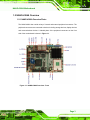
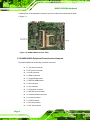
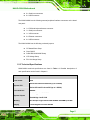
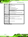
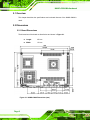
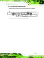

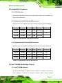


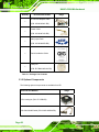

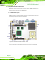


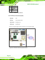
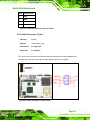
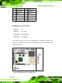
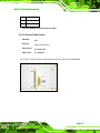
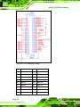
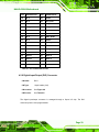
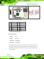

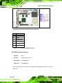
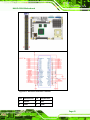
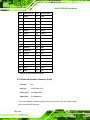
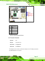
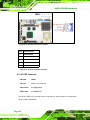

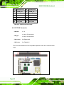
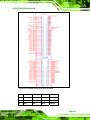
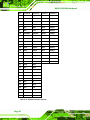

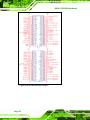
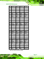
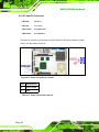
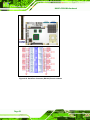
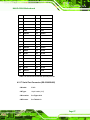

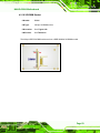
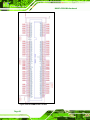
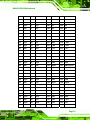
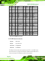
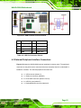
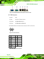
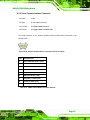
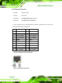
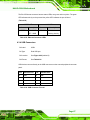
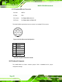
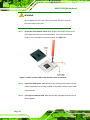
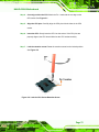
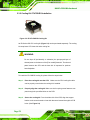
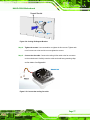
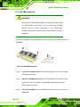
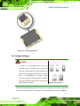
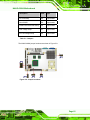
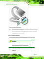
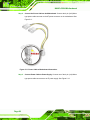


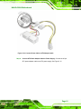
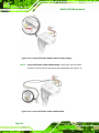
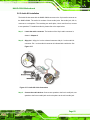
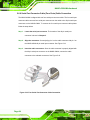
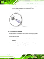
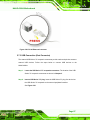
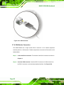

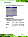
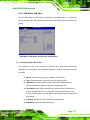


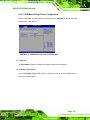

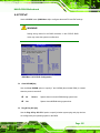
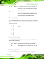

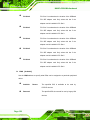
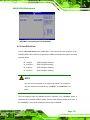
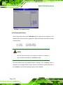
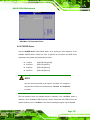
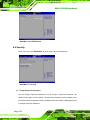
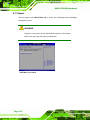
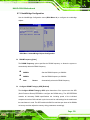
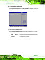
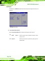

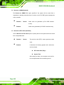
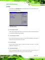


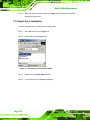
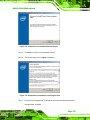
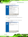
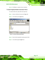
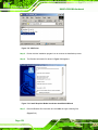
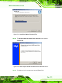
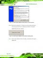
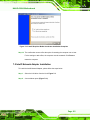
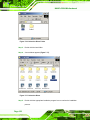
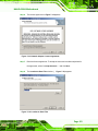
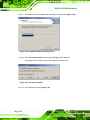

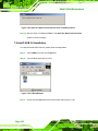
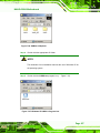
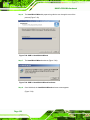


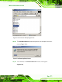

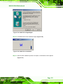
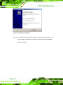


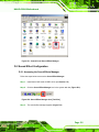


![RUMD User Manual [Version 3.0]](http://vs1.manualzilla.com/store/data/005734566_1-539a984f38202face31c4a646ef91457-150x150.png)