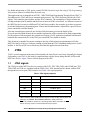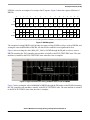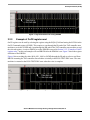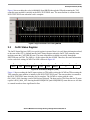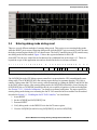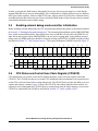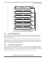
1
Freescale Semiconductor Application Note Document Number: AN4365 Rev. 0, 09/2011 Qorivva MPC56xx Flash Programming Through Nexus/JTAG by: Andrew Turner 32-bit Applications Engineering Microcontroller Solutions Group The Qorivva MPC56xx family of devices has internal flash memory used for code and data. The MPC56xx Nexus debug interface can be used to program flash memory using the JTAG communication protocol through the JTAG port. This allows programming of the internal flash memory with an external tool. All MPC56xx devices have versions of the e200zx core that support variable length encoding (VLE) instructions. Most MPC56xx devices support both Book E and VLE instructions; however, some MPC560x devices utilize the e200z0 core that only supports VLE instructions. Table 9 shows the core types used on currently available MPC56xx devices. However, as different variations of the MPC56xx family will be released during the lifecycle of this document, it is important that you confirm the core type on the target MPC56xx device. For the remainder of this document, code examples are provided in Book E. If the instruction example differs when implemented in VLE, the equivalent VLE instruction is also shown in brackets. © Freescale Semiconductor, Inc., 2011. All rights reserved. Contents 1 JTAG . . . . . . . . . . . . . . . . . . . . . . . . . . . . . . . . . . . . . . . . 2 2 On-Chip Emulation (OnCE) . . . . . . . . . . . . . . . . . . . . . . . 6 3 Nexus read/write access block . . . . . . . . . . . . . . . . . . . 22 4 System initialization . . . . . . . . . . . . . . . . . . . . . . . . . . . . 27 5 Creating the flash programming tool . . . . . . . . . . . . . . . 29 6 References . . . . . . . . . . . . . . . . . . . . . . . . . . . . . . . . . . 34 7 Revision history . . . . . . . . . . . . . . . . . . . . . . . . . . . . . . . 34 Appendix A Demo calling basic SSD functions. . . . . . . . . . . . . . . . . . . . . 35 JTAG For further information on VLE, please consult VLEPM, Variable-Length Encoding (VLE) Programming Environments Manual, available from freescale.com. This application note is adapted from AN3283, “MPC5500 Flash Programming Through Nexus/JTAG.” It first addresses the JTAG and Nexus communication protocol. The JTAG discussion includes the JTAG signals, TAP controller state machine, and the JTAG controller. The explanation of Nexus includes the on-chip emulation (OnCE) module and the Nexus read/write (R/W) access block. As different versions of the MPC56xx devices may use different JTAG and Nexus modules, the examples given here are generic to suit this flash memory programming note. If more detailed information is required for a specific device, please consult the reference manual. After the communication protocols are described, this document goes into the details of the Freescale-provided flash memory drivers and the requirements of the external tool for flash programming. For the purpose of this document, the external tool consists of a PC application combined with interface hardware that connects the PC to the JTAG port on an MPC56xx board or module. This document is intended for anyone wanting to develop a flash memory programming tool for the MPC56xx family of devices. Someone wanting to learn about the JTAG communication protocol, OnCE module, or the Nexus R/W access block may also find this application note beneficial. 1 JTAG JTAG is a serial communication protocol developed by the Joint Test Access Group. Originally developed for boundary scan, JTAG is also used for communication with the Nexus debug interface (NDI) on the MPC56xx devices. Figure 2 shows a block diagram of the NDI. 1.1 JTAG signals The JTAG port of the MPC56xx devices consists of the TCK, TDI, TDO, TMS, and JCOMP pins. TDI, TDO, TMS, and TCK are compliant with the IEEE 1149.1-2001 standard and are shared with the NDI through the test access port (TAP) interface. See Table 1 for signal properties. Table 1. JTAG signal properties Name I/O Function TCK I Test Clock TDI I Test Data In TDO O Test Data Out TMS I Test Mode Select JCOMP1 I JTAG Compliancy O Nexus/JTAG Ready 2 RDY 1 JCOMP is not available on all MPC56xx devices. In devices without a JCOMP pin, the JTAG controller is always enabled and can only be reset by clocking TCK five times with TMS high. See AN4088, “MPC5500/MPC5600 Nexus Support Overview.” 2 RDY is not available on all devices or all package types. When unavailable, the RDY feature cannot be used to accelerate Nexus block move options Qorivva MPC56xx Flash Programming Through Nexus/JTAG, Rev. 0 Freescale Semiconductor 2 JTAG 1.2 TAP controller state machine The TAP controller state machine controls the JTAG logic. The TAP controller state machine is a 16-state finite state machine (FSM) as shown in Figure 1. The TCK and TMS signals control transition between states of the FSM. These two signals control whether an instruction register scan or data register scan is performed. Both the TDI and TMS inputs are sampled on the rising edge of TCK while the TDO output changes on the falling edge of TCK. The value shown next to each state of the state machine in Figure 1 is the value of TMS required on the rising edge of TCK to transition to the connected state. Five rising edges of TCK with TMS at logic 1 guarantees entry into the TEST LOGIC RESET state. Qorivva MPC56xx Flash Programming Through Nexus/JTAG, Rev. 0 Freescale Semiconductor 3 JTAG Figure 1. TAP controller finite state machine Qorivva MPC56xx Flash Programming Through Nexus/JTAG, Rev. 0 Freescale Semiconductor 4 JTAG 1.3 JTAG Controller (JTAGC) The devices in the MPC56xx family have a JTAG controller (JTAGC) that enables both boundary scan and communication with the Nexus Development Interface (NDI). A block diagram of the NDI is shown in Figure 2. Cache Off-Chip Memory & I/O eTPU Engine 1 MMU Engine 2* XBAR On-Chip Memory & I/O e200z6 CDC eDMAC NDEDI NZ6C3 R/W Register, Halt, Step, Continue Program, Data, Ownership, Watchpoint, Trace FlexRay NXDM R/W Register, R/W Data, Halt, Step, Continue Program, Data, Ownership, Watchpoint, Trace NXFR Data, Watchpoint, Trace Data, Watchpoint, Trace Read/Write Access Buffer Buffer JTAG Port Controller (JTAGC) Nexus Port Controller (NPC) Buffer Buffer Auxiliary Port ••• JCOMP RDY TDI TCK TDO TMS EVTI MSEO[0:1] MCKO MDO(4 or 12) EVTO * Some MPC55xx devices have one eTPU engine, others have two engines. Figure 2. Nexus Development Interface (NDI) functional block diagram 1.3.1 JTAGC reset The JTAGC is placed in reset when the TAP controller state machine is in the test logic reset state. The test logic reset state is entered upon the assertion of the power-on reset signal, negation of JCOMP, or through TAP controller state machine transitions controlled by TMS. Asserting power-on reset or negating JCOMP results in asynchronous entry into the test logic reset state. In devices without a JCOMP pin, the JTAGC is always enabled and can only be reset by clocking TCK five times with TMS high. See AN4088, “MPC5500/MPC5600 Nexus Support Overview” for a table of devices that implement the JCOMP pin. Qorivva MPC56xx Flash Programming Through Nexus/JTAG, Rev. 0 Freescale Semiconductor 5 On-Chip Emulation (OnCE) 1.3.2 TAP sharing The JTAGC allows communication with the NDI by sharing the test access port (TAP) with other TAP controllers. The JTAGC initially has control of the TAP after the assertion of power-on reset or the negation of JCOMP. As an example, selectable NDI TAP controllers for the MPC5674F include the Nexus port controller, e200z7 OnCE, eTPU Nexus, and eDMA Nexus. The NDI TAP controllers are selected by loading the appropriate opcode into the 5-bit instruction register of the JTAGC while JCOMP is asserted. Table 2 shows the opcodes for the selectable TAP controllers. The JTAGC instructions available will vary slightly depending on the core type of the MPC56xx device being programmed; however, the important factor in the context of this flash memory programming note is that the ACCESS_AUX_TAP_ONCE opcode is the same on all MPC56xx devices. For further details on the device-specific JTAGC instructions, please consult the individual reference manual When one of these opcodes is loaded, control of the TAP pins is transferred to the selected auxiliary TAP controller. Any data input via TDI and TMS is passed to the selected TAP controller, and any TDO output from the selected TAP controller is sent back to the JTAGC to be output on the TDO pin. The JTAGC regains control of the TAP during the UPDATE-DR state if the PAUSE-DR state was entered. Auxiliary TAP controllers are held in RUN-TEST/IDLE while they are inactive. This document will focus on the OnCE TAP controller. While access to the other TAP controllers is similar, they are outside the scope of this document and are not needed for flash memory programming. Table 2. Selected JTAG client select instructions 2 JTAGC Instruction Opcode Description ACCESS_AUX_TAP_NPC 10000 Enables access to the NPC TAP controller ACCESS_AUX_TAP_ONCE 10001 Enables access to the e200z7 OnCE TAP controller ACCESS_AUX_TAP_eTPU 10010 Enables access to the eTPU Nexus TAP controller ACCESS_AUX_TAP_NXDM 10011 Enables access to the eDMA_A Nexus TAP controller ACCESS_AUX_TAP_NXFR 10100 Enables access to the FlexRay Nexus TAP controller On-Chip Emulation (OnCE) All of the MPC56xx devices possess a OnCE module for debug control of the PowerPC® e200zx core. The OnCE logic provides static debug capability including run-time control, register access, and memory access to all memory-mapped regions including on-chip peripherals. The OnCE module is controlled by the JTAG signals through the OnCE TAP controller. 2.1 Enabling the OnCE TAP Controller Control of the OnCE module is obtained through the OnCE TAP controller. To enable the OnCE TAP controller, the JTAGC must have control of the TAP and the ACCESS_AUX_TAP_ONCE (0b10001) opcode must be loaded into the 5-bit JTAGC instruction register with the JCOMP signal set to a logic 1. The JTAGC instruction register is loaded by scanning in the appropriate bits on the TDI pin, least significant bit (LSB) first, while in the SHIFT-IR state of the TAP controller state machine shown in Figure 1. The last bit is shifted in with TMS set to a logical 1 causing transition from the SHIFT-IR state Qorivva MPC56xx Flash Programming Through Nexus/JTAG, Rev. 0 Freescale Semiconductor 6 On-Chip Emulation (OnCE) to the EXIT1-IR state. Table 3 shows the steps required to enable the OnCE TAP controller, assuming the TAP controller state machine is initially in the RUN-TEST/IDLE state. The state machine is returned to the RUN-TEST/IDLE state when the write is complete. Table 3. Steps for enabling the OnCE TAP controller TCK Tick TMS 1 TDI1 Resulting state 1 1 X SELECT-DR-SCAN 2 1 X SELECT-IR-SCAN 3 0 X CAPTURE-IR 4 0 X SHIFT-IR 5 0 1 SHIFT-IR 6 0 0 SHIFT-IR 7 0 0 SHIFT-IR 8 0 0 SHIFT-IR 9 1 1 EXIT1-IR 10 1 X UPDATE-IR 11 0 X RUN-TEST/IDLE A value of X signifies that the signal value does not matter. Figure 3 shows the required signal transitions on a logic analyzer for enabling the OnCE TAP controller. Figure 3. Signal transitions for enabling the OnCE TAP controller 2.2 OnCE register access The OnCE module provides several registers for static debug support. The OnCE Command register (OCMD) is a special register and acts as the IR for the TAP controller state machine and is used to access other OnCE resources. Qorivva MPC56xx Flash Programming Through Nexus/JTAG, Rev. 0 Freescale Semiconductor 7 On-Chip Emulation (OnCE) 2.2.1 OnCE Command register The OnCE Command register (OCMD) is a 10-bit shift register that receives its serial data from the TDI pin and acts as the IR register of the TAP controller state machine. The OCMD is updated when the TAP controller enters the UPDATE-IR state. It contains fields for controlling access to a resource, as well as controlling single step operations and exit from debug mode. Figure 4 shows the register definition for the OnCE command register. Table 4 and Table 5 display the bit definitions for the command register and register addressing selection, respectively. 0 1 2 R/W GO EX 3 4 5 6 7 8 9 RS[0:6] Reset - 0b10_0000_0010 on assertion of JCOMP, during power on reset, or while in the TEST LOGIC RESET state Figure 4. OnCE Command register (OCMD) Table 4. OCMD bit definitions Bit(s) Name Description 0 R/W Read/Write Command bit The R/W bit specifies the direction of data transfer. 0 Write the data associated with the command into the register specified by RS[0:6] 1 Read the data contained in the register specified by RS[0:6] Note: The R/W bit is ignored for read-only or write-only registers. In addition, it is ignored for all bypass operations. When performing writes, most registers are sampled in the Capture-DR state into a 32-bit shift register, and subsequently shifted out on TDO during the first 32 clocks of Shift-DR. 1 GO Go Command bit 0 Inactive (no action taken) 1 Execute instruction in IR If the GO bit is set, the chip will execute the instruction that resides in the IR register in the CPUSCR. To execute the instruction, the processor leaves debug mode, executes the instruction, and if the EX bit is cleared, returns to debug mode immediately after executing the instruction. The processor goes on to normal operation if the EX bit is set, and no other debug request source is asserted. The GO command is executed only if the operation is a read/write to CPUSCR or a read/write to “No Register Selected.” Otherwise, the GO bit is ignored. The processor will leave debug mode after the TAP controller Update-DR state is entered. On a GO + NoExit operation, returning to debug mode is treated as a debug event, thus exceptions such as machine checks and interrupts may take priority and prevent execution of the intended instruction. Debug firmware should mask these exceptions as appropriate. The OSR[ERR] bit indicates such an occurrence. Qorivva MPC56xx Flash Programming Through Nexus/JTAG, Rev. 0 Freescale Semiconductor 8 On-Chip Emulation (OnCE) Table 4. OCMD bit definitions (continued) Bit(s) Name Description 2 EX Exit Command bit 0 Remain in debug mode 1 Leave debug mode If the EX bit is set, the processor will leave debug mode and resume normal operation until another debug request is generated. The Exit command is executed only if the Go command is issued, and the operation is a read/write to CPUSCR or a read/write to “No Register Selected.” Otherwise, the EX bit is ignored. The processor will leave debug mode after the TAP controller Update-DR state is entered. Note that if the DR bit in the OnCE control register is set or remains set, or if a bit in the DBSR is set, or if a bit in the DBSR is set and DBCR0[EDM]=1 (external debug mode is enabled), then the processor may return to debug mode without execution of an instruction, even though the EX bit was set. 3–9 RS Register Select The Register Select bits define which register is source (destination) for the read (write) operation. Attempted writes to read-only registers are ignored. Table 5 shows the OnCE register address. This example is taken from an e200z7 core MPC56xx device. Some of the registers shown may not be available on devices with other cores. However, the registers used for flash memory programming are identical across all MPC56xx e200zx cores. Only the DBCR0[EDM] is accessible in the DBCR0 register prior to that bit being set. Setting DBCR0[EDM] enables external debug mode and disables software updates to debug registers. The CPU should be placed in debug mode via the OCR[DR] bit prior to setting the DBCR0[EDM] bit. For more information on enabling external debug mode, see Section 2.5, “Enabling external debug mode and other initialization.” Table 5. OnCE register addressing (e200z7 core) OCMD, RS[0:6] Register selected 000 0000—000 0001 Invalid value 000 0010 JTAG DID (read-only) 000 0011—000 1111 Invalid value 001 0000 CPU Scan Register (CPUSCR) 001 0001 No register selected (bypass) 001 0010 OnCE Control Register (OCR) 001 0011—001 1111 Invalid value 010 0000 Instruction Address Compare 1 (IAC1) 010 0001 Instruction Address Compare 2 (IAC2) 010 0010 Instruction Address Compare 3 (IAC3) 010 0011 Instruction Address Compare 4 (IAC4) 010 0100 Data Address Compare 1 (DAC1) 010 0101 Data Address Compare 2 (DAC2) 010 0110 Data Value Compare 1 (DVC1) Qorivva MPC56xx Flash Programming Through Nexus/JTAG, Rev. 0 Freescale Semiconductor 9 On-Chip Emulation (OnCE) Table 5. OnCE register addressing (e200z7 core) (continued) OCMD, RS[0:6] 2.2.2 Register selected 010 0111 Data Value Compare 2 (DVC2) 010 1000 Instruction Address Compare 5 (IAC5) 010 1001 Instruction Address Compare 6 (IAC6) 010 1010 Instruction Address Compare 7 (IAC7) 010 1011 Instruction Address Compare 8 (IAC8) 010 1100 Debug Counter Register (DBCNT) 010 1101 Debug PCFIFO (PCFIFO) (read-only) 010 1110 External Debug Control Register 0 (EDBCR0) 010 1111 External Debug Status Register 0 (EDBSR0) 011 0000 Debug Status Register (DBSR) 011 0001 Debug Control Register 0 (DBCR0) 011 0010 Debug Control Register 1 (DBCR1) 011 0011 Debug Control Register 2 (DBCR2) 011 0100 Debug Control Register 3 (DBCR3) 0011 0101 Debug Control Register 4 (DBCR4) 011 0110 Debug Control Register 5 (DBCR5) 011 0111 Debug Control Register 6 (DBCR6) 011 1000—011 1100 Invalid value (do not access) 011 1101 Debug Data Acquisition Message Register (DDAM) 011 1110 Debug Event Control (DEVENT) 011 1111 Debug External Resource Control (DBERC0) 111 0000—111 1001 General Purpose Register Selects [0:9] 111 1010 Cache Debug Access Control Register (CDACNTL) 111 1011 Cache Debug Access Data Register (CDADATA) 111 1100 Nexus3 access 111 1101 LSRL select 111 1110 Enable_OnCE (and bypass) 111 1111 Bypass Example of OnCE register write OnCE registers can be written by selecting the register using the RS[0:6] field and clearing the R/W bit in the OnCE Command register (OCMD). This requires a scan through the IR path of the TAP controller state machine to write the OCMD and a scan through the DR path of the TAP controller state machine to write the selected register. As mentioned above, the external debug mode bit, DBCR0[EDM], must be set to a logical 1 to allow access to most of the OnCE registers. Therefore, writing the DCBR0 register to set the Qorivva MPC56xx Flash Programming Through Nexus/JTAG, Rev. 0 Freescale Semiconductor 10 On-Chip Emulation (OnCE) EDM bit is used as an example of a writing a OnCE register. Figure 5 shows the register definition of DBCR0. 0 1 2 R EDM IDM 3 RST 4 5 6 7 8 9 ICMP BRT IRPT TRAP IAC1 IAC2 10 11 IAC3 IAC4 12 13 DAC1 14 15 DAC2 W Reset 01 0 0 0 0 0 0 0 0 0 0 0 0 0 0 0 16 17 18 19 20 21 22 23 24 25 26 27 28 29 30 31 0 0 0 0 0 0 0 0 FT 0 0 0 0 0 0 0 0 0 R RET DEVT1 DEVT2 DCNT1 DCNT2 CIRPT CRET W Reset 0 0 0 0 0 0 0 1DBCR0[EDM] is affected by a Nexus port reset or a power on reset, but not by an assertion of RESET. All other bits are reset by processor reset (including assertion of RESET) as well as by a power on reset. Figure 5. DBCR0 register The example of writing DBCR0 is divided into two parts: writing OCMD to select a write to DBCR0, and writing the value 0x80000000 to DBCR0. All data will be scanned in least significant bit first. Figure 6 shows writing the value 0b00_0011_0001 to OCMD through the IR path to select a write to DBCR0 assuming the TAP controller state machine is initially in the RUN-TEST/IDLE state. The state machine is returned to the RUN-TEST/IDLE state when the write is complete. Figure 6. Signal transitions for writing OCMD to select a write to DBCR0 Figure 7 shows writing the value 0x80000000 to DBCR0 through the DR path to set the EDM bit assuming the TAP controller state machine is initially in the RUN-TEST/IDLE state. The state machine is returned to the RUN-TEST/IDLE state when the write is complete. Qorivva MPC56xx Flash Programming Through Nexus/JTAG, Rev. 0 Freescale Semiconductor 11 On-Chip Emulation (OnCE) Figure 7. Signal transitions for writing DBCR0 2.2.3 Example of OnCE register read OnCE registers can be read by selecting the register using the RS[0:6] field and setting the R/W bit in the OnCE Command register (OCMD). This requires a scan through the IR path of the TAP controller state machine to write the OCMD and a scan through the DR path of the TAP controller state machine to read the selected register. A write to DBCR0 to set the EDM bit was used in Section 2.2.2, “Example of OnCE register write,” so this read example will read DBCR0 after the EDM bit is set. Figure 5 shows the register definition of the DBCR0. Figure 8 shows writing the value 0b10_0011_0001 to OCMD through the IR path to select a read from DBCR0 assuming the TAP controller state machine is initially in the RUN-TEST/IDLE state. The state machine is returned to the RUN-TEST/IDLE state when the write is complete. Figure 8. Signal transitions for writing OCMD to select a read from DBCR0 Qorivva MPC56xx Flash Programming Through Nexus/JTAG, Rev. 0 Freescale Semiconductor 12 On-Chip Emulation (OnCE) Figure 9 shows reading the value 0x80000000 from DBCR0 through the DR path assuming the TAP controller state machine is initially in the RUN-TEST/IDLE state. The state machine is returned to the RUN-TEST/IDLE state when the read is complete. Figure 9. Signal transitions for reading DBCR0 2.3 OnCE Status Register The OnCE Status Register (OSR) is a special register in terms of how it is read. Status information related to the state of the CPU is latched into the OnCE Status Register when the OnCE TAP controller state machine enters the CAPTURE-IR state. The status information is shifted out serially through the SHIFT-IR state on TDO. The OSR is a 10-bit register like the OCMD. Therefore, the status information can be read while writing OCMD. The OSR is shown in Figure 10. 0 1 2 3 4 5 6 MCLK ERR CHKSTOP RESET HALT STOP DEBUG 7 8 0 9 1 Figure 10. OnCE Status Register (OSR) Figure 11 shows reading the OnCE status register on TDO while writing the OCMD on TDI assuming the TAP controller state machine is initially in the RUN-TEST/IDLE state. The state machine is returned to the RUN-TEST/IDLE state when the read is complete. The OCMD is written with the value 0b10_0001_0001 choosing a read of No Register Selected. The data read on TDO from the OnCE status register is 0b10_0000_1001 showing that the OSR[MCLK] and OSR[DEBUG] status bits are set. All data is scanned in and out least significant bit first. Qorivva MPC56xx Flash Programming Through Nexus/JTAG, Rev. 0 Freescale Semiconductor 13 On-Chip Emulation (OnCE) Figure 11. Signal transitions of reading the OnCE Status Register 2.4 Entering debug mode during reset There are several different methods of entering debug mode. This section covers entering debug mode while the RESET pin is asserted. Entering debug mode while the RESET pin is asserted is useful, because the debug session begins with the CPU in a known state. The OnCE Control Register (OCR) controls entry into debug mode for this method. Figure 12 shows the register definition for the OCR. 5 6 7 8 0 9 10 11 12 13 14 15 16 DMDIS 17 18 0 19 20 21 22 23 24 25 26 27 28 0 29 30 WKUP FDB 31 DR 4 DE 3 DG 2 DM 1 DW 0 DI Some MPC56xx devices with a Harvard architecture have additional bits in the range 0–15. These are beyond the scope of this application note and are detailed in the device reference manuals. Reset - 0x0000_0000 on negation of JCOMP, power on reset, or entering TEST LOGIC RESET state Figure 12. OnCE Control Register (OCR) The OCR[DR] bit is the CPU debug request control bit; it requests that the CPU unconditionally enter debug mode. The OCR[WKUP] bit is the wakeup request bit used to guarantee that the CPU clock is running. Debug status and CPU clock activity can be determined by reading the DEBUG and MCLK bits in the OnCE status register. After entering debug mode, the OCR[DR] bit should be cleared leaving the OCR[WKUP] bit set. OCR[FDB] should also then be set to enable recognition of software breakpoints. See Section 2.12.1, “Software breakpoints,” for details on software breakpoints. The steps required for entering debug mode during reset assuming the OnCE TAP controller has been enabled via the method described in Section 2.1, “Enabling the OnCE TAP Controller,” are listed below: 1. Assert RESET. 2. Set the OCR[DR] and OCR[WKUP] bits. 3. Deassert RESET. 4. Verify debug mode via the DEBUG bit in the OnCE status register. 5. Clear the OCR[DR] bit while leaving OCR[WKUP] set and set OCR[FDB]. Qorivva MPC56xx Flash Programming Through Nexus/JTAG, Rev. 0 Freescale Semiconductor 14 On-Chip Emulation (OnCE) In order to program the flash memory through the Nexus port, the boot mode must be set such that the internal flash and Nexus state are both enabled. This is determined in slightly different ways on different MPC56xx family members. Some use BOOTCFG pins, whereas others use FAB (Force Alternate Boot) and ABS (Alternate Boot Selector) pins. Please consult the BAM chapter of the relevant reference manual for detailed information on boot mode setting. 2.5 Enabling external debug mode and other initialization Before enabling external debug mode, the CPU should be placed into debug mode via the method outlined in Section 2.4, “Entering debug mode during reset.” The external tool should then write the DBCR0[EDM] bit to enable external debug mode. Note that the first write to DBCR0 will only affect the EDM bit. All other bits in that register require DBCR0[EDM] to be set prior to writing them. After enabling external debug mode, the DBSR status bits should be cleared by writing 0xFFFFFFFF to DBSR using the method described in Section 2.2, “OnCE register access.” The register definition of DBSR is shown in Figure 13. 0 R IDE 1 2 UDE 3 MRR 4 5 ICMP BRT 6 7 IRPT TRAP 8 9 10 IAC1 IAC2 IAC3 W Reset 12 13 14 15 IAC4 DAC1 DAC1 DAC2 DAC2 R W R W 0 0 0 1 0 0 0 0 0 0 0 0 0 0 0 0 16 17 18 19 20 21 22 23 24 25 26 27 28 29 30 31 0 0 0 0 0 0 0 0 CNT1 RG 0 0 0 0 0 0 0 0 0 R RET W Reset 11 0 DEVT DEVT DCNT DCNT CIRP CRET 1 2 1 2 T 0 0 0 0 0 0 Figure 13. Debug Status Register (DBSR) 2.6 CPU Status and Control Scan Chain Register (CPUSCR) CPU information is accessible via the OnCE module through a single scan chain register named the CPUSCR. The CPUSCR provides access to this CPU information and a mechanism for an external tool to set the CPU to a desired state before exiting debug mode. The CPUSCR also provides the ability to access register and memory contents. Figure 14 shows the CPUSCR. Once debug mode has been entered, it is required to scan in and update the CPUSCR prior to exiting debug mode or single stepping. Access to the CPUSCR is controlled by the OCMD as described in Section 2.2, “OnCE register access.” Qorivva MPC56xx Flash Programming Through Nexus/JTAG, Rev. 0 Freescale Semiconductor 15 On-Chip Emulation (OnCE) TDO 32 0 31 WBBR TCK low 32 0 WBBR 31 TDI high 32 0 MSR 31 32 0 PC 31 32 0 IR 31 32 0 CTL 31 Figure 14. CPU Status and Control Scan Chain Register 2.6.1 Instruction Register (IR) After entering debug mode, the opcode of the next instruction to be executed will be in the Instruction Register (IR). The value in the IR should be saved for later restoration if continuation of the normal instruction stream is desired. The external tool has the capability to put instructions directly into the IR via the CPUSCR. These instructions can then be executed by the debug control block. By selecting appropriate instructions and single stepping them, the external tool can examine or change memory locations or CPU registers. See Section 2.7, “Single step,” for details on single step. 2.6.2 Control State register (CTL) The Control State register (CTL) stores the value of certain internal CPU state variables before debug mode is entered. Figure 15 shows the CTL register. Some MPC56xx devices have additional bit fields populated in the bit range 0–15. These bits are not important in the context of this document. For further information, please see the relevant e200zx core guide, available at www.freescale.com. Qorivva MPC56xx Flash Programming Through Nexus/JTAG, Rev. 0 Freescale Semiconductor 16 On-Chip Emulation (OnCE) PCOFST IRSTAT9 11 12 13 14 15 16 17 18 19 20 21 22 23 24 25 26 27 28 29 30 31 IRSTAT8 10 IRSTAT7 * 9 IRSTAT6 8 IRSTAT5 7 IRSTAT4 6 IRSTAT3 5 IRSTAT2 4 IRSTAT1 3 IRSTAT0 2 FFRA 1 PCINV 0 Figure 15. Control State Register (CTL) The “*” in the CTL register represents internal processor state bits that should be restored to the value they held when debug mode was entered prior to exiting debug mode. If a single step is executing an instruction that is in the normal instruction flow of the program that was running when debug mode was entered, these bits should be restored. If a single step is executing an instruction outside the normal instruction flow, these bits should be cleared to zero. The PCOFST field indicates whether the value in the PC portion of the CPUSCR must be adjusted prior to exiting debug mode. Due to the pipelined nature of the CPU, the PC value must be backed-up under certain circumstances. The PCOFST field specifies the value to be subtracted from the PC value when debug mode was entered. This PC value should be adjusted according to PCOFST prior to exit from debug mode if continuation of the normal instruction stream is desired. In the event that PCOFST is non-zero, the IR should be loaded with a no-op instruction instead of the value in the IR when debug mode was entered. The preferred no-op instruction is ori 0,0,0 (0x60000000). Using VLE the preferred no-op is e_ori 0,0,0 (0x1800D000). Below are the possible values and meanings of the PCOFST field. 0000 = No correction required. 0001 = Subtract 0x04 from PC. 0010 = Subtract 0x08 from PC. 0011 = Subtract 0x0C from PC. 0100 = Subtract 0x10 from PC. 0101 = Subtract 0x14 from PC. All other encodings are reserved. After entering debug mode, the PCINV field overrides the PCOFST field and indicates if the values in the PC and IR are invalid. If PCINV is 1, then exiting debug mode with the saved values in the PC and IR will have unpredictable results. Debug firmware should initialize the PC and IR values in the CPUSCR with desired values before exiting debug if this bit was set when debug mode was initially entered. 0 = No error condition exists. 1 = Error condition exists. PC and IR are corrupted. The FFRA control bit causes the contents of WBBR to be used as the rA (rS for logical and shift operations) operand value of the first instruction to be executed when exiting debug mode or the instruction to be single stepped. This allows the external tool to update CPU registers and memory. rA and rS are instruction syntax used to identify a source GPR. 0 = No action. 1 = Contents of WBBR used as rA (rS for logical and shift operations) operand value. Qorivva MPC56xx Flash Programming Through Nexus/JTAG, Rev. 0 Freescale Semiconductor 17 On-Chip Emulation (OnCE) The IRStat0-9 bits provide status information to the external tool. The IRStat8 bit indicates that the instruction in the IR is a VLE or non-VLE instruction. For MPC56xx devices with an e200z0 core only VLE instructions are used and this bit is reserved. 0 = IR contains a BookE instruction. 1 = IR contains a PowerPC VLE instruction, aligned in the most significant portion of IR if 16-bit. 2.6.3 Program Counter register (PC) The PC stores the value of the program counter that was present when debug mode was entered. The PC value is affected by operations performed during debug mode and must be restored prior to exiting debug mode. It may be necessary to adjust the PC before exiting debug mode according the PCOFST field in the CTL. If the external tool wants to redirect program flow to an arbitrary location, the PC and IR should be initialized corresponding to the first instruction to be executed. Alternatively, the IR may be set to a no-op instruction and the PC may be set to the location prior to the location at which it is desired to redirect flow. When debug mode is exited, the no-op will execute and then instruction fetch and execution will begin at the location which it is desired to redirect flow. 2.6.4 Write-Back Bus Register (WBBRlow, WBBRhigh) WBBR is used as a means of passing operand information to/from the CPU from/to the external tool. Whenever the external tool needs to read the contents of a CPU register or memory location, it can force the CPU to single step an instruction that brings that information to WBBR. To write the contents of a CPU register or memory location, the external tool can force the CPU to single step an instruction that uses the information in WBBR. For the purpose of this document, only WBBRlow will be used. WBBRhigh is used for SPE instructions that generate 64-bit results or use 64-bit operands. Such instructions are outside the scope of this document. 2.6.5 Machine State Register (MSR) The MSR is used to read/write the machine state register of the CPU. This register is affected by operations performed while in debug mode. If consistency of the machine state is desired, the MSR should be saved when entering debug mode and restored prior to exiting debug mode. 2.7 Single step Single stepping of instructions is achieved by first placing the CPU in debug mode if the CPU is not already in debug mode. The next step is to write the appropriate information into the CPU scan chain register (CPUSCR), followed by writing to OCMD to set the OCMD[GO] bit and clear the OCMD[EX] bit with the OCMD[RS] field indicating either the CPUSCR or No Register Selected. The CPUSCR register is covered in Section 2.6, “CPU Status and Control Scan Chain Register (CPUSCR).” Once debug mode has been entered, it is required that a scan in and update to the CPUSCR must be performed prior to single stepping. For single step, the CPU will return to debug mode after executing a single instruction. The external tool should read the OnCE Status Register (OSR) to verify that the CPU has returned to debug mode with no Qorivva MPC56xx Flash Programming Through Nexus/JTAG, Rev. 0 Freescale Semiconductor 18 On-Chip Emulation (OnCE) error by verifying that the OSR[DEBUG] bit is set and OSR[ERR] bit is cleared. For details on reading the OSR, see Section 2.3, “OnCE Status Register.” During single step, exception conditions can occur, if not masked, and may prevent the desired instruction from being executed. After stepping over the instruction, the core will fetch the next instruction. The new program counter and instruction will be loaded into the PC and IR portions of the CPUSCR. Care must be taken to insure that the next instruction fetch after the single step is to a valid memory location. See Section 4.1, “Setting up the memory management unit,” and Section 4.2, “Internal SRAM initialization,” for details. For MPC56xx devices with Book E and VLE capable cores, the CTL[IRstat8] bit indicates that the instruction in the IR is a VLE or non-VLE instruction. For MPC56xx devices with an e200z0 core, only VLE instructions are available and the CTL[IRstat8] is reserved. The CTL[FFRA], CTL[IRStat8], and the CTL bits indicated by “*” should be set as appropriate before single stepping. All other CTL bits should be set to zero. See Section 2.6.2, “Control State register (CTL),” for details on FFRA, IRStat8, and the bits indicated by “*”. Single stepping can be used during normal execution of the instruction flow or to force execution of a particular instruction by loading the desired instruction into the IR portion of the CPUSCR. By forcing execution of particular instructions, single stepping can be used for memory and register access by the tool. See Section 2.11, “OnCE memory access,” Section 2.9, “GPR access,” and Section 2.10, “SPR access,” for details. 2.8 Exit from debug mode to normal execution Exiting debug mode and returning to normal execution is achieved by first clearing the OCR[DMDIS] and OCR[DR] bits if not already clear while leaving the OCR[MCLK] set. The next step is to write the appropriate information into the CPU scan chain register (CPUSCR), followed by a write to OCMD to set the OCMD[GO] bit and OCMD[EX] bit with the OCMD[RS] field indicating either the CPUSCR or No Register Selected. Once debug mode has been entered, it is required that a scan in and update to the CPUSCR be performed prior to exiting debug mode. The CPUSCR register is covered in Section 2.6, “CPU Status and Control Scan Chain Register (CPUSCR).” If continuation of the normal instruction stream is desired, the external tool is responsible for inspection of the CTL register value when debug mode was entered to determine if the PC is invalid or needs to be offset prior to exiting debug mode. Also, the internal state bits indicated by “*” in the CTL should be restored to their original value when debug mode was entered if continuation of the normal instruction stream is desired. The IRStatus bits of the CTL should be set to zero with the exception of CTL[IRStat8] on MPC56xx devices with VLE (MPC56xx devices with e200z0 cores are only VLE instructions). CTL[IRStat8] indicates if the current instruction in the IR is a VLE or non-VLE instruction. See Section 2.6.2, “Control State register (CTL),” for details. To begin instruction execution from an arbitrary location, which is the case when executing the Freescale-provided flash memory drivers, the PC should be set to the desired location for execution to begin minus 0x4. The IR should be set to a no-op (ex: Book E=0x60000000 VLE =1800D000), then exit debug mode as mentioned above. The no-op will be executed, then the core will begin fetching instructions at the desired location for execution. Qorivva MPC56xx Flash Programming Through Nexus/JTAG, Rev. 0 Freescale Semiconductor 19 On-Chip Emulation (OnCE) 2.9 GPR access The OnCE module provides the ability to read and write the general purpose registers (GPR) while in debug mode. Reading a general purpose register is achieved by single stepping over an ori instruction. As an example, to read the lower 32 bits of GPR r1, an ori r1,r1,0 instruction is executed (for VLE e_ori r1,r1,0), and the result of the instruction will be latched into WBBRlow. The external tool can then read the contents of WBBRlow by scanning out the CPUSCR. Writing a register is achieved by single stepping over an ori (for VLE e_ori) instruction with the CTL[FFRA] bit set causing the WBBRlow to be used as the source register for the instruction. As an example, to write the lower 32 bit of GPR r1, an ori r1, X, 0 (VLE e_ori r1,X,0) is executed with the data to be written in WBBRlow. The X in the instruction will be replaced by the WBBRlow register. See Section 2.7, “Single step,” for details on single stepping. 2.10 SPR access The OnCE module provides the ability to read and write the special purpose registers (SPR) while in debug mode. Reading a special purpose register is achieved by saving the value in a GPR, single stepping over a mfspr instruction which brings the SPR value into both the saved GPR and WBBRlow, and then restoring the GPR. As an example, to read SPR 624, first save r31. Then execute mfspr r31, 624. The value that was in SPR 624 will now be in WBBRlow of the CPUSCR and can be read by the external tool. Finally r31 should be restored. To write an SPR, single step over a mtspr instruction with the value to write to the SPR in WBBRlow and the CTL[FFRA] bit set. For example, to write SPR 624 with the value 0x10050000, single step over mtspr 624, X with the value to write to SPR 624 in WBBRlow and CTL[FFRA] set. The X in the instruction will be replaced by WBBRlow. See Section 2.7, “Single step,” for details on single stepping. DBCR0–3, DBSR, DBCNT, IAC1–4, and DAC1–2 cannot be written by single stepping over mtspr like the other SPRs while in external debug mode. They can, however, be written by the method detailed in Section 2.2, “OnCE register access.” 2.11 OnCE memory access There are two ways to access memory mapped locations on the MPC56xx devices: one is through the OnCE module, and the other is through the Nexus R/W access block. The OnCE module method requires that the CPU be in debug mode and make use of the memory management unit (MMU) and cache. The Nexus R/W access block does not require that the CPU be in debug mode and bypasses the MMU and cache. The Nexus R/W access block is also the faster method of accessing memory. This section covers access to memory mapped locations using the OnCE method. The Nexus R/W access block is covered in Section 3, “Nexus read/write access block.” Writing a memory location is achieved by first reading the contents of a GPR and saving that value, writing that GPR with the value to be written to memory, and single stepping over a stw, sth, or stb (VLE e_stw, e_sth, e_stb) instruction with the address to write in WBBRlow and the CTL[FFRA] bit set. The GPR that was previously saved should be used as the rS field of the store instruction. After single stepping over the store instruction, the saved GPR value should then be restored. For example, to write the word 0xA5A5A5A5 to location 0x40000000, first save the value in a r31. Then write the value 0xA5A5A5A5 Qorivva MPC56xx Flash Programming Through Nexus/JTAG, Rev. 0 Freescale Semiconductor 20 On-Chip Emulation (OnCE) to r31. The next step is to step over the instruction stw r31, 0(X) with 0x40000000 in WBBRlow and the CTL[FFRA] bit set. The X in the instruction is replaced by the WBBRlow register. GPR r31 should then be restored to its saved value. Reading a memory location is achieved by first reading the contents of a GPR and saving that value, then single stepping a lwz, lhz, or lbz (VLE e_lwz, e_lhz, e_lbz) with the address to be read in WBBRlow and the CTL[FFRA] bit set. The GPR that was previously saved should be used as the rD field of the load instruction. The value read from the memory location will then be in both the WBBRlow and the GPR whose value was previously saved. After single stepping the load instruction and getting the read data from WBBRlow, the saved GPR value should then be restored. For example, to read a word from address location 0x40000000, first save the value in r31. Then single step over the instruction lwz r31, 0(X) with 0x40000000 in WBBRlow and the CTL[FFRA] bit set. The X in the instruction is replaced by the WBBRlow register. After the single step is complete, the data read from memory can be read by the external tool from WBBRlow. GPR r31 should then be restored to its saved value. See Section 2.7, “Single step,” for details on single stepping. 2.12 Breakpoints The OnCE debug module provides the capability for both software and hardware breakpoints to be set at a particular address. For Flash programming using the Freescale provided Flash drivers, software breakpoints are the easiest to use. As a reference, instruction address hardware breakpoints will also be discussed in this section. 2.12.1 Software breakpoints Recognition of software breakpoints by the OnCE module are enabled by setting the OCR[FDB] bit along with the DBCR0[EDM] bit. Upon executing a bkpt pseudo-instruction, the CPU enters debug mode after the instruction following the bkpt pseudo-instruction has entered the instruction register. The bkpt pseudo-instruction is defined to be an all zeroes instruction opcode. The Freescale-provided flash memory drivers have the bkpt pseudo-instruction built in and execution of this instruction at the completion of the driver can be enabled or disabled. This feature of the drivers is discussed in Section 5.2.2, “FlashInit.” 2.12.2 Instruction address hardware breakpoints The OnCE module provides the capability to set up four instruction address hardware breakpoints. When an instruction address breakpoint is hit, the CPU will enter debug mode prior to executing the instruction at that address location. When debug mode is entered due to a breakpoint, the CPUSCR will hold the address at which the breakpoint was set in the PC, and the IR will contain the instruction at that address. To use an instruction address hardware breakpoint, the following steps are required: 1. Write the address at which a breakpoint is desired to one of the instruction address compare registers IAC1, IAC2, IAC3, or IAC4. Some MPC56xx devices have more than four IAC registers, up to a maximum of eight. 2. Enable the instruction address compare debug event in the DBCR0 by setting the appropriate enable bit; DBCR0[IAC1], DBCR0[IAC2], DBCR0[IAC3], or DBCR0[IAC4]. 3. Exit from debug mode to normal execution to execute the desired code. Qorivva MPC56xx Flash Programming Through Nexus/JTAG, Rev. 0 Freescale Semiconductor 21 Nexus read/write access block 4. Poll the DBSR for the appropriate status bit to be set; DBSR[IAC1], DBSR[IAC2], DBSR[IAC3], or DBSR[IAC4]. Figure 13 shows the register definition of DBSR. 5. If the appropriate status bit in DBSR is set, verify entry into debug mode by reading the OnCE status register. 6. Clear the appropriate status bit by writing a 1 to that bit location in the DBSR; DBSR[IAC1], DBSR[IAC2], DBSR[IAC3], or DBSR[IAC4]. 3 Nexus read/write access block The Nexus module provided on the cores of the MPC56xx family of devices offers the capability for program trace, data trace, ownership trace, watchpoint messaging and trigger, and read/write (R/W) access to memory mapped regions. This section covers R/W access using the Nexus R/W access block. The other features of the Nexus module are beyond the scope of this document and will not be covered. Some versions of the MPC56xx devices with an e200z0 core do not have a Nexus read/write access block. Further details can be found in AN4088, “MPC5500/MPC5600 Nexus Support Overview.” Unlike the OnCE method of memory access, the Nexus R/W access block provides the ability to read and write memory without having to stop code execution by entering debug mode. The Nexus R/W access method provides faster memory access over the OnCE method due to fewer JTAG scans, and it doesn’t require loading and single stepping over any instructions. The Nexus R/W access block is independent of the CPU and therefore bypasses the MMU and cache. The R/W access block is controlled by three Nexus registers. These registers are the Read/Write Access Control/Status register (RWCS), Read/Write Access Data register (RWD), and Read/Write Access Address register (RWA). Access to the Nexus registers is covered in Section 3.1, “Nexus register access.” RWCS is shown in Figure 17 and Table 6 gives the field descriptions. 31 R AC 30 29 RW 28 27 26 SZ 25 24 23 MAP 22 PR 21 20 19 18 17 16 BST 0 0 0 0 0 W Reset 0 0 0 0 0 0 0 0 Nexus Reg 0 0 0 0 0 0 0 0 7 6 5 4 3 2 1 0 ERR DV 0 0 0x7 15 14 13 12 11 10 9 R 8 CNT W Reset 0 Nexus Reg 0 0 0 0 0 0 0 0 0 0 0 0 0 0x7 Figure 16. Read/Write Access Control/Status register (RWCS) Qorivva MPC56xx Flash Programming Through Nexus/JTAG, Rev. 0 Freescale Semiconductor 22 Nexus read/write access block Table 6. RWCS field description Bit(s) Name Description 31 AC Access control. 0 End access 1 Start access 30 RW Read/write select. 0 Read access 1 Write access 29–27 SZ [2:0] Word size. 000 8-bit (byte) 001 16-bit (half-word) 010 32-bit (word) 011 64-bit (double-word - only in burst mode) 100–111 Reserved (default to word) 26–24 MAP [2:0] MAP select. 000 Primary memory map 001–111 Reserved 23–22 PR [1:0] Read/write access priority. 00 Lowest access priority 01 Reserved (default to lowest priority) 10 Reserved (default to lowest priority) 11 Highest access priority 21 BST Burst control. 0 Module accesses are single bus cycle at a time. 1 Module accesses are performed as burst operation. 20–16 — 15–2 CNT [13:0] Access control count. Number of accesses of word size SZ. 1 ERR Read/write access error. See Table 7. 0 DV Reserved. Read/write access data valid. See Table 7. Table 7 details the status bit encodings. Table 7. Read/Write Access Status Bit Encoding Read action Write action ERR DV Read access has not completed Write access completed without error 0 0 Read access error has occurred Write access error has occurred 1 0 Read access completed without error Write access has not completed 0 1 Not allowed Not allowed 1 1 The Read/Write Access Data register is shown in Figure 17. Qorivva MPC56xx Flash Programming Through Nexus/JTAG, Rev. 0 Freescale Semiconductor 23 Nexus read/write access block 31 30 29 28 27 26 25 R 24 23 22 21 20 19 18 17 16 0 0 0 0 0 0 0 0 7 6 5 4 3 2 1 0 0 0 0 0 0 0 0 Read/Write Data W Reset 0 0 0 0 0 0 0 0 Nexus Reg 0xA 15 14 13 12 11 10 9 R 8 Read/Write Data W Reset 0 0 0 0 0 0 0 0 Nexus Reg 0 0xA Figure 17. Read/Write Access Data register (RWD) The Read/Write Access Address register is shown in Figure 18. 31 30 29 28 27 26 R 25 24 23 22 21 20 19 18 17 16 Read/Write Address W Reset 0 0 0 0 0 0 0 0 Nexus Reg 0 0 0 0 0 0 0 0 7 6 5 4 3 2 1 0 0 0 0 0 0 0 0x9 15 14 13 12 11 10 R 9 8 Read/Write Address W Reset 0 0 0 0 0 Nexus Reg 0 0 0 0 0 0x9 Figure 18. Read/Write Access Address register (RWA) 3.1 Nexus register access Access to the Nexus registers is enabled by loading the Nexus3-Access instruction (0b00_0111_1100) into the OCMD. See Section 2.2.1, “OnCE Command register,” for details on the OCMD. Once the Nexus3-Access instruction has been loaded, reading/writing a Nexus register requires two passes through the DR path of the OnCE TAP controller state machine, detailed below. For details on the TAP controller state machine, see Section 1.2, “TAP controller state machine.” 1. The first pass through the DR selects the Nexus register to be accessed and whether the access will be a read or a write. This is achieved by loading an 8-bit value LSB first into the JTAG Data Register (DR). This register has the following format: Qorivva MPC56xx Flash Programming Through Nexus/JTAG, Rev. 0 Freescale Semiconductor 24 Nexus read/write access block (7 bits) Nexus Register Index (1 bit) R/W RESET value: 0x00 Nexus register index Read/Write (R/W): Value shown at bottom of register description 0 Read 1 Write 2. The second pass through the DR then shifts the data in or out depending on the type of access. Data is always shifted LSB first. a) During a read access, the data is latched from the Nexus register when the TAP controller state machine passes through the CAPTURE-DR state. The data from the Nexus register can be read by the external tool by shifting the data out in the SHIFT-DR state. The last bit is shifted out with TMS set to 1, causing a transition to the EXIT1-DR state. b) During a write access, the data is shifted in while in the SHIFT-DR state. The last bit is shifted in with TMS set to 1, causing transition to the EXIT1-DR state. The data is latched into the Nexus register when the TAP controller state machine passes through the UPDATE-DR state. 3.2 Single memory write access The steps to perform a single memory write access via the Nexus R/W access block are: 1. Initialize RWA with the address to be written using Nexus register index 0x9. 2. Initialize RWCS using Nexus register index 0x7. a) Access Control (AC) = 0b1 (to indicate start access) b) Map Select (MAP) = 0b000 (primary memory map) c) Access Priority (PR) = 0b00 (lowest priority) d) Read/Write (RW) = 0b1 (write access) e) Word Size (SZ) = 0b000 (8-bit) or 0b001 (16-bit) or 0b010 (32-bit) f) Access Count (CNT) = 0b00_0000_0000_0000 or 0b00_0000_0000_0001 (single access) g) Burst Control (BST) = 0b0 (burst disabled) 3. Initialize RWD using Nexus register index 0xA with the data to be written to the address in RWA. The endianess of the data needs to be right-justified little endian. — 8-bit value of 0xDE to be written to memory: RWD = 0x000000DE — 16-bit value of 0xDEAD to be written to memory: RWD = 0x0000ADDE — 32-bit value of 0xDEADBEEF to be written to memory: RWD = 0xEFBEADDE Qorivva MPC56xx Flash Programming Through Nexus/JTAG, Rev. 0 Freescale Semiconductor 25 Nexus read/write access block 4. The Nexus block will then arbitrate for the system bus and transfer the data value from RWD to the memory mapped address in RWA. When the access has completed without error, then RWCS[ERR] = 0 and RWCS[DV] = 0. See Table 7 for details. This indicates that the device is ready for the next access. Nexus will also assert the RDY pin when the transaction has completed without error. The external tool can use this as an alternative to polling the RWCS status bits. 3.3 Burst block memory write access The steps to perform a burst block memory write access via the Nexus R/W access block are: 1. Initialize RWA with the first address to be written using Nexus register index 0x9. The address needs to be aligned on an 8-byte boundary. RWA[2:0] are ignored on a burst write. 2. Initialize RWCS using Nexus register index 0x7. a) Access Control (AC) = 0b1 (to indicate start access) b) Map Select (MAP) = 0b000 (primary memory map) c) Access Priority (PR) = 0b00 (lowest priority) d) Read/Write (RW) = 0b1 (write access) e) Word Size (SZ) = 0b011 (64-bit) f) Access Count (CNT) = 0b00_0000_0000_0100 (four double-words) g) Burst Control (BST) = 0b1 (burst enabled) 3. Write all 32 bytes of data to be burst to RWD using Nexus register index 0xA, 32 bits at a time, starting with the first 32-bit word to be written to the address in RWA. This data will be buffered internally by the burst data buffer. The endianess of the 32-bit data written to RWD needs to be little endian. — Value of 0xDEADBEEF to be written to memory: RWD = 0xEFBEADDE 4. The Nexus block will then arbitrate for the system bus and transfer the burst data from the burst data buffer to the memory starting at the address in RWA. When the access has completed without error, then RWCS[ERR] = 0 and RWCS[DV] = 0. See Table 7 for details. This indicates that the device is ready for the next access. Nexus will also assert the RDY pin when the transaction has completed without error. The external tool can use this as an alternative to polling the RWCS status bits. 3.4 Single memory read access The steps to perform a single memory read access via the Nexus R/W access block are: 1. Initialize RWA with the address to be read using the register index 0x9. 2. Initialize RWCS using Nexus register index 0x7. a) Access Control (AC) = 0b1 (to indicate start access) b) Map Select (MAP) = 0b000 (primary memory map) c) Access Priority (PR) = 0b00 (lowest priority) d) Read/Write (RW) = 0 (read access) e) Word Size (SZ) = 0b000 (8-bit) or 0b001 (16-bit) or 0b010 (32-bit) Qorivva MPC56xx Flash Programming Through Nexus/JTAG, Rev. 0 Freescale Semiconductor 26 System initialization f) Access Count (CNT) = 0b00_0000_0000_0000 or 0b00_0000_0000_0001 (single access) g) Burst Control (BST) = 0b0 (burst disabled) 3. The Nexus block will then arbitrate for the system bus and the read data will be transferred to RWD from the memory mapped address in RWA. When the access has completed without error, then RWCS[ERR] = 0 and RWCS[DV] = 1. See Table 7 for details. This indicates that the device is ready for the next access. Nexus will also assert the RDY pin when the transaction has completed without error. The external tool can use this as an alternative to polling the RWCS status bits. 4. The data can then be read from the RWD register using Nexus register index 0xA. The data in RWD will be right-justified little endian. — 8-bit value of 0xDE read from memory: RWD = 0x000000DE — 16-bit value of 0xDEAD read from memory: RWD = 0x0000ADDE — 32-bit value of 0xDEADBEEF read from memory: RWD = 0xEFBEADDE 3.5 Burst block memory read access The steps to perform a burst block memory read access via the Nexus R/W access block are: 1. Initialize RWA with the first address to be read using Nexus register index 0x9. The address needs to be aligned on an 8-byte boundary. RWA[2:0] are ignored on a burst read. 2. Initialize RWCS using Nexus register index 0x7. a) Access Control (AC) = 0b1 (to indicate start access) b) Map Select (MAP) = 0b000 (primary memory map) c) Access Priority (PR) = 0b00 (lowest priority) d) Read/Write (RW) = 0b0 (read access) e) Word Size (SZ) = 0b011 (64-bit) f) Access Count (CNT) = 0b00_0000_0000_0100 (four double-words) g) Burst Control (BST) = 0b1 (burst enabled) 3. The Nexus block will then arbitrate for the system bus and transfer the burst data from memory to the burst data buffer starting at the address in RWA. When the access has completed without error then RWCS[ERR] = 0 and RWCS[DV] = 1. See Table 7 for details. This indicates that the device is ready for the next access. Nexus will also assert the RDY pin when the transaction has completed without error. The external tool can use this as an alternative to polling the RWCS status bits. 4. Read all 32 bytes of data from RWD using Nexus register index 0xA, 32 bits at a time, starting with the first 32-bit word read from the address in RWA. The endianess of the 32-bit data read from RWD will be little endian. — Value of 0xDEADBEEF read from memory: RWD = 0xEFBEADDE 4 System initialization For flash memory programming, there is some system initialization that needs to be performed by the external tool. This initialization includes setting up the memory management unit (MMU), initializing the internal SRAM, and configuring the frequency modulated phase-locked loop (FMPLL). Qorivva MPC56xx Flash Programming Through Nexus/JTAG, Rev. 0 Freescale Semiconductor 27 System initialization 4.1 Setting up the memory management unit MPC56xx devices with an e200z0 core do not have a memory management unit (MMU). The memory locations are permanently mapped and setting up the MMU is not required. The MMU on the non-e200z0 MPC56xx devices provides access protection to memory mapped regions as well as memory translation from effective to real addresses. For the purpose of flash memory programming, it is easiest to setup the MMU such that the effective addresses are the same as the real addresses. For the CPU to access a memory mapped region, an MMU entry for that memory space must be configured. The external tool has the capability to setup MMU entries by writing the appropriate SPRs and single stepping over the tlbwe instruction. For flash memory programming, the external tool should set up at least four MMU entries. The steps required to setup an MMU entry are: 1. Set up MAS0 (SPR 624). 2. Set up MAS1 (SPR 625). 3. Set up MAS2 (SPR 626). 4. Set up MAS3 (SPR 627). 5. Execute tlbwe (0x7C0007A4). The minimum set of four MMU entries required is detailed in Table 8. This example for setting up the MMU is for an external tool using the Freescale provided non-VLE Flash drivers running from internal SRAM. For the VLE driver set, MAS2 value for the internal SRAM should be 0x40000028 to enable the MAS2[VLE] bit. Table 8. MAS register settings for MMU setup Memory region MAS0 MAS1 MAS2 MAS3 PBridge B1 0x10000000 0xC0000500 0xFFF0000A 0xFFF0003F Internal SRAM 0x10010000 0xC0000400 0x400000082 0x4000003F PBridge A 0x10020000 0xC0000500 0xC3F00008 0xC3F0003F Internal flash 0x10030000 0xC0000700 0x00000000 0x0000003F 1 The PBridge B MMU entry is not required for flash memory programming, but this MMU entry in addition to the others allows access to the entire memory map of the MPC56xx devices. 2 Set Internal SRAM MAS2 value to 0x40000028 when using the VLE driver set. 4.2 Internal SRAM initialization The MPC56xx family of devices all contain internal SRAM that must be initialized after power-on reset by 64-bit writes to the entire memory. This is necessary to initialize the error-correcting code (ECC) logic. The easiest way to do this with an external tool is to single step over a number of stmw (VLE e_stmw) (store multiple words) instructions with r0 as the rS field, the address to begin the writes in WBBRlow, and CTL[FFRA] set. See Section 2.7, “Single step,” for details on single step. This will cause all 32 GPRs to be written to memory beginning at the address in WBBRlow using 64-bit writes. For example, the starting physical address of the internal SRAM is 0x40000000. Stepping over stmw r0, 0(X) with the 0x40000000 Qorivva MPC56xx Flash Programming Through Nexus/JTAG, Rev. 0 Freescale Semiconductor 28 Creating the flash programming tool in WBBRlow will cause all 32 GPRs to be written to memory starting at address 0x40000000 using 64-bit writes. Then 0x80 should be added to the address, written to WBBRlow, and stmw executed again. This should be done [size of internal SRAM] [0x80] times to initialize the entire internal SRAM. The MMU must be configured prior to initializing the internal SRAM. See Section 4.1, “Setting up the memory management unit,” for details. 4.3 FMPLL initialization For correct flash memory operation, the system frequency needs to be greater than 25 MHz and less than the specified maximum operating frequency of the device being programmed. The FMPLL configuration methods are similar across the MPC55xx/MPC56xx families but some MPC56xx devices have slight variations. It is advisable to refer to the pertinent reference manual to set the PLL to the desired frequency. Device-specific examples for setting the PLL are provided in AN2865, “MPC5500 & MPC5600 Simple Cookbook.” 5 Creating the flash programming tool This section covers the flash memory drivers provided by Freescale, describes the tool requirements, and also suggests a functional division of the tool. 5.1 Flash programming drivers Freescale provides a set of flash memory drivers for each of the MPC56xx devices. The flash memory drivers are available from the Freescale website for each individual device. Table 9 shows the flash drivers used for each MPC56xx device available at the time of writing. Please consult the Freescale website for the latest drivers. A user’s manual is also installed with the drivers. These drivers are easy to use and well documented. The drivers come in a c-array, s-record, and library format. For external tools, the s-record format is the easiest to use. Instructions on how to use the s-record format set of drivers are included in the next section. There are also examples of how to use the three driver formats provided with the installation of the SSD. Table 9. MPC56xx flash memory standard driver and e200zx core family type1 MPC 56xx device Freescale SSD flash driver Core type MPC5668G C90FL_SSD e200z6 MPC5604E C90LC_SSD e200z0* MPC560xB C90LC_JDP_SSD e200z0* MPC560xP C90LC_JDP_SSD e200z0* MPC560xS C90LC_JDP_SSD e200x0* MPC563xM C90LC_JDP_SSD e200z3 MPC564xA MPC5644A_ C90FL_JDP_SSD e200z4 Qorivva MPC56xx Flash Programming Through Nexus/JTAG, Rev. 0 Freescale Semiconductor 29 Creating the flash programming tool Table 9. MPC56xx flash memory standard driver and e200zx core family type1 MPC564xL C90FL_JDP_SSD e200z4 MPC567xF MPC_5674F_MPC5676F_C90FL_ SSD e200z7 MPC567XK MPC567XK_C90LC_FLASH_SSD e200z7 MPC5676R MPC5674F_MPC5676F_C90FL_SSD e200z7 1 Devices with e200z0 cores must use only VLE instructions. 5.2 Tool requirements The flash programming tool must perform several required tasks to program the flash memory on the MPC56xx devices. 5.2.1 Debug and driver initialization The first requirement is to enter debug mode followed by the appropriate initialization. These steps must be performed every time a reset occurs or a new MPC56xx device is connected to the flash programming tool. The steps to do this are listed below. 1. Ensure that the JTAGC currently has control of the TAP by going through the PAUSE-DR state. See Section 1.3.2, “TAP sharing,” for details. 2. Enable the OnCE TAP controller by the method outlined in Section 2.1, “Enabling the OnCE TAP Controller.” 3. Enter debug mode during reset and enable recognition of software breakpoints as mentioned in Section 2.4, “Entering debug mode during reset.” 4. Enable external debug mode and clear the debug status bits as mention in Section 2.5, “Enabling external debug mode and other initialization.” 5. Setup the MMU as described in Section 4.1, “Setting up the memory management unit.” 6. Initialize the internal SRAM as mentioned in Section 4.2, “Internal SRAM initialization.” 7. Initialize the FMPLL as mentioned in Section 4.3, “FMPLL initialization.” The next step is to load the s-record format flash driver set. The required drivers to load are FlashInit, SetLock, FlashProgram, and FlashErase. The other drivers are not required but could be loaded if features other than erasing and programming are desired. The s-record drivers all specify a start address of 0x0; however, the drivers are position independent. The tool should load each driver into internal SRAM at a desired location. The tool is responsible for knowing where these drivers are located in memory. Space should also be reserved in the internal SRAM for variables needed for the driver set. For example, the SSD_CONFIG structure is used for all drivers. Space must be allocated for this structure. Space should also be allocated in internal SRAM for the stack and a buffer for the data to be programmed to flash memory. The drivers and variables can be written by the method described in Section 2.11, “OnCE memory access,” or Section 3, “Nexus read/write access block.” Qorivva MPC56xx Flash Programming Through Nexus/JTAG, Rev. 0 Freescale Semiconductor 30 Creating the flash programming tool An example of the s-record demo for the C90LC flash driver is shown in Appendix A, “Demo calling basic SSD functions,” to illustrate how parameters are passed to the flash driver functions used in the next steps. 5.2.2 FlashInit After the drivers are loaded into internal SRAM, operations on the flash memory can begin. The FlashInit driver should be called first to initialize the flash memory. The steps required are outlined below. 1. Set up the SSD_CONFIG structure as required. This is documented in the SSD user’s manual. YOu should correctly initialize the fields XXXXRegBase (replace XXXX with the relevant flash memory module such as C90LC or C90FL), mainArrayBase, shadowRowBase, shadowRowSize, pageSize, and BDMEnable. The other fields will be initialized when FlashInit is executed. BDMEnable should be set to 1 to cause debug mode to be entered via a software breakpoint when each driver completes execution. This is the easiest way for the external tool to determine when driver execution is complete. 2. Set up r1 as the stack pointer by writing r1 using the method described in Section 2.9, “GPR access.” 3. Set up r3 to point to the SSD_CONFIG structure in internal SRAM. 4. Set the PC to the beginning of FlashInit minus 0x4 and load the IR with a no-op (ex: Book E=0x60000000 VLE =1800D000). See Section 2.6, “CPU Status and Control Scan Chain Register (CPUSCR)” for details. 5. Exit debug mode and begin execution of the driver as described in Section 2.8, “Exit from debug mode to normal execution.” 6. Poll the OnCE Status Register to determine when debug mode has been re-entered. Reading the OnCE Status Register is described in Section 2.3, “OnCE Status Register.” 7. When debug mode has been entered, read the return value in r3. Possible return values and their meanings are discussed in the SSD user’s manual. Reading a GPR is explained in Section 2.9, “GPR access.” 5.2.3 SetLock After the flash memory has been initialized using the FlashInit function, the SetLock function should be called as many times as required to unlock or lock the appropriate flash memory blocks. For the low and mid blocks as well as the shadow block, the lock bits in both the primary and secondary lock registers must be set appropriately. It is recommended that the shadow block be locked unless programming of the shadow block is absolutely necessary. Erasing the shadow block without reprogramming the censorship information prior to a reset will cause the device to be censored. The steps to call the SetLock driver are listed below. 1. Set up r1 as the stack pointer. 2. Set up r3 to point to the SSD_CONFIG structure in internal SRAM. 3. Set up r4 with the lock indicator as documented in the SSD user’s manual. 4. Set up r5 with the lock state as documented in the SSD user’s manual. Qorivva MPC56xx Flash Programming Through Nexus/JTAG, Rev. 0 Freescale Semiconductor 31 Creating the flash programming tool 5. 6. 7. 8. 9. 5.2.4 Set up r6 with the correct password as documented in the SSD user’s manual. Set the PC to the beginning of SetLock minus 0x4 and load the IR with a no-op. Exit debug mode and begin execution of the driver. Poll the OnCE Status Register to determine when debug mode has been re-entered. When debug mode has been entered, read the return value in r3. Possible return values and their meanings are discussed in the SSD user’s manual. FlashErase When the appropriate blocks have been locked or unlocked, then an erase of the unlocked blocks can be performed. The steps to call the FlashErase driver are listed below. 1. Set up r1 as the stack pointer. 2. Set up r3 to point to the SSD_CONFIG structure in internal SRAM. 3. Set up r4 to indicate either the main array or shadow block to be erased as describes in the SSD user’s manual. Erasing the shadow block without reprogramming the censorship control information prior to a reset will result in the device being censored. 4. Set up r5 to select the low address array blocks to be erased as documented in the SSD user’s manual. 5. Set up r6 to select the mid address array blocks to be erased as documented in the SSD user’s manual. 6. Set up r7 to select the high address array blocks to be erased as documented in the SSD user’s manual. 7. Set up r8 with the pointer to the call back function as documented in the SSD user’s manual. 8. Set the PC to the beginning of FlashErase minus 0x4 and load the IR with a no-op. 9. Exit debug mode and begin execution of the driver. 10. Poll the OnCE Status Register to determine when debug mode has been re-entered. 11. When debug mode has been entered, read the return value in r3. Possible return values and their meanings are discussed in the SSD user’s manual. 5.2.5 FlashProgram When flash memory blocks have been erased, they then can be programmed. To program the flash, the internal SRAM should first be written with the data to be programmed in flash memory. Depending on the size of the data buffer in internal SRAM and the size of the data to be programmed to flash, the FlashProgram driver may need to be called multiple times. The steps to call the FlashProgram driver are listed below. 1. Set up r1 as the stack pointer. 2. Set up r3 to point to the SSD_CONFIG structure in internal SRAM. 3. Set up r4 to point to the destination address to be programmed in flash memory. This address must be aligned on a double word boundary. Qorivva MPC56xx Flash Programming Through Nexus/JTAG, Rev. 0 Freescale Semiconductor 32 Creating the flash programming tool 4. Set up r5 to the size of the data in bytes to be programmed to flash memory. This size should be a multiple of 8 and the combination of the destination address and size should be entirely contained in the main array or shadow block. 5. Set up r6 to point to the source buffer of data in internal SRAM to be programmed to flash memory. This address should be aligned on a word boundary. 6. Set up r7 with the pointer to the call back function as documented in the SSD user’s manual. 7. Set the PC to the beginning of FlashProgram minus 0x4 and load the IR with a no-op. 8. Exit debug mode and begin execution of the driver. 9. Poll the OnCE Status Register to determine when debug mode has been re-entered. 10. When debug mode has been entered, read the return value in r3. Possible return values and their meanings are discussed in the SSD user’s manual. 5.2.6 Using other drivers There are other useful drivers provided with the driver set. For example, BlankCheck can be used to verify that a particular region is erased, and ProgramVerify can be used to verify that the data was programmed correctly. The method to use these other drivers is similar to the above mentioned drivers except that the GPRs will need to be setup appropriately for that particular driver. 5.3 Functional division of the external tool Before creating the external tool for flash memory programming, thought should be given to how the software should be divided to meet the tool’s functional requirements. The following list gives an example of a simple functional division of the software: • OnCE TAP controller enable, see Section 2.1, “Enabling the OnCE TAP Controller.” • OnCE register read, see Section 2.2, “OnCE register access.” • OnCE register write, see Section 2.2, “OnCE register access.” • OnCE status register read, see Section 2.3, “OnCE Status Register.” • Debug mode during reset, see Section 2.4, “Entering debug mode during reset.” • Single step, see Section 2.7, “Single step.” • Exit from debug mode, see Section 2.8, “Exit from debug mode to normal execution.” • Write GPR, see Section 2.9, “GPR access.” • Read GPR, see Section 2.9, “GPR access.” • Write SPR, see Section 2.10, “SPR access.” • Read SPR, see Section 2.10, “SPR access.” • OnCE memory read, see Section 2.11, “OnCE memory access.” • OnCE memory write, see Section 2.11, “OnCE memory access.” • Nexus3 single write, see Section 3.2, “Single memory write access.” • Nexus3 burst write, see Section 3.3, “Burst block memory write access.” • Nexus3 single read, see Section 3.2, “Single memory write access.” Qorivva MPC56xx Flash Programming Through Nexus/JTAG, Rev. 0 Freescale Semiconductor 33 References • • • • • • • • • • Nexus3 burst read, see Section 3.5, “Burst block memory read access.” MMU initialization, see Section 4.1, “Setting up the memory management unit.” Internal SRAM initialization, see Section 4.2, “Internal SRAM initialization.” FMPLL initialization, see Section 4.3, “FMPLL initialization.” S-record parser and loader. Debug and driver initialization, see Section 5.2.1, “Debug and driver initialization.” Flash initialization, see Section 5.2.2, “FlashInit.” Flash block lock initialization, see Section 5.2.3, “SetLock.” Flash erase, see Section 5.2.4, “FlashErase.” Flash program, see Section 5.2.5, “FlashProgram.” 6 References For further information, please refer to the documents listed in Table 10. Table 10. References Document Title Availability AN2865 MPC5500 & MPC5600 Simple Cookbook AN3283 MPC5500 Flash Programming Through Nexus/JTAG AN3968 Nexus Interface Connector for the MPC567xF and MPC5676R Families AN4088 MPC5500/MPC5600 Nexus Support Overview e200z0CORERM e200z0 Power Architecture® Core Reference Manual e200z1RM e200z1 Power Architecture Core Reference Manual e200z3CORERM e200z1 Power Architecture Core Reference Manual e200z4RM e200z4 Power Architecture Core Reference Manual e200z6RM e200z6 PowerPC Core Reference Manual e200z760RM e200z760 Power Architecture Core Reference Manual 7 www.freescale.com Revision history Table 11. Changes made April 20121 Section Description Front page Add SafeAssure branding. Title and text on first page Add Qorivva branding. Back page Apply new back page format. 1 No substantive changes were made to the content of this document; therefore the revision number was not incremented. Qorivva MPC56xx Flash Programming Through Nexus/JTAG, Rev. 0 Freescale Semiconductor 34 Demo calling basic SSD functions Appendix A Demo calling basic SSD functions This is a demo for the LC flash driver included in the flash driver. A similar example is provided in each of the other Freescale flash drivers. ;************************************************************************* ;* (c) Copyright Freescale Semiconductor & STMicroelectronics Inc. 2011 * ; All Rights Reserved * ;************************************************************************* ; ;************************************************************************* ;* * ;* Standard Software Driver for C90lc(2) * ;* * ;* FILE NAME : demo.mac * ;* DESCRIPTION : This file shows how to call basic SSD functions. * ;* DATE : May 18, 2011 * ;* AUTHOR : FPT Team * ;* * ;* * ;*************************************************************************/ ; ;******************************* CHANGES ********************************* ; 0.1.0 05.18.2010 FPT Team Initial Version ;*************************************************************************/ ;1. Demo with SSD in S-record format; ; ;2. Demo 8 S-record format SSD functions: ; FlashInit FlashInit.sx ; FlashErase FlashErase.sx ; BlankCheck BlankCheck.sx ; FlashProgram FlashProgram.sx ; ProgramVerify ProgramVerify.sx ; CheckSum CheckSum.sx ; GetLock GetLock.sx ; SetLock SetLock.sx ; ;3. RAM Mapping of SSD S-record demo ; Start Address End Address Size (Byte) ; --------------------------------------------------------------------------; FlashInit $40000000 $40000300-1 $300 ; FlashErase $40000300 $40000A00-1 $700 ; BlankCheck $40000A00 $40000D00-1 $300 ; FlashProgram $40000D00 $40001B00-1 $E00 ; ProgramVerify $40001B00 $40001E00-1 $300 ; CheckSum $40001E00 $40002100-1 $300 ; GetLock $40002100 $40002600-1 $500 ; SetLock $40002600 $40002A00-1 $400 ; ; Demo data $40004000 $40004200-1 $200 ; Data buffer $40005000 $40005800-1 $800 ; Stack $40007000 $40008000-1 $1000 ; ; *********************************************************************** Qorivva MPC56xx Flash Programming Through Nexus/JTAG, Rev. 0 Freescale Semiconductor 35 Demo calling basic SSD functions ; Start to initialize variables for demo and download SSD. ; Start to initialize variables for demo and download SSD. Please wait... ; Set return code symbol C90LC_OK symbol C90LC_ERROR_ALIGNMENT symbol C90LC_ERROR_RANGE symbol C90LC_ERROR_BUSY symbol C90LC_ERROR_PGOOD symbol C90LC_ERROR_EGOOD symbol C90LC_ERROR_NOT_BLANK symbol C90LC_ERROR_VERIFY symbol C90LC_ERROR_LOCK_INDICATOR symbol C90LC_ERROR_RWE symbol C90LC_ERROR_PASSWORD symbol C90LC_ERROR_AIC_MISMATCH symbol C90LC_ERROR_AIC_NO_BLOCK symbol C90LC_ERROR_FMR_MISMATCH symbol C90LC_ERROR_FMR_NO_BLOCK symbol C90LC_ERROR_ECC_LOGIC symbol C90FL_ERROR_SUSP ; word symbol symbol symbol symbol symbol $00000000 $00000100 $00000200 $00000300 $00000400 $00000500 $00000600 $00000700 $00000800 $00000900 $00000A00 $00000B00 $00000C00 $00000D00 $00000E00 $00000F00 $00001000 size, double word size and page size in byte C90LC_WORD_SIZE $4 C90LC_DWORD_SIZE $8 C90LC_PAGE_SIZE_04 $4 C90FL_PAGE_SIZE_08 $8 C90FL_PAGE_SIZE_16 $16 ; Indicators for symbolting/getting block lock state symbol LOCK_SHADOW0_PRIMARY $0 symbol LOCK_SHADOW0_SECONDARY $1 symbol LOCK_LOW_PRIMARY $2 symbol LOCK_LOW_SECONDARY $3 symbol LOCK_MID_PRIMARY $4 symbol LOCK_MID_SECONDARY $5 symbol LOCK_HIGH $6 ; values for TRUE and FALSE symbol TRUE symbol FALSE $1 $0 ; NULL callback symbol NULL_CALLBACK $FFFFFFFF ; Array space lock enabled password symbol FLASH_LMLR_PASSWORD $A1A11111 symbol FLASH_HLR_PASSWORD $B2B22222 symbol FLASH_SLMLR_PASSWORD $C3C33333 ; Set the RAM mapping symbol RAM_BASE symbol SSD_BASE symbol SSD_SIZE symbol DEMO_DATA_BASE symbol DEMO_DATA_SIZE symbol BUFFER_BASE $40000000 $40000000 $4000 $40004000 $200 $40005000 Qorivva MPC56xx Flash Programming Through Nexus/JTAG, Rev. 0 Freescale Semiconductor 36 Demo calling basic SSD functions symbol BUFFER_SIZE symbol STACK_BASE symbol STACK_SIZE $800 $40007000 $1000 ; Set addresses of each function symbol Addr_FlashInit symbol Addr_FlashErase symbol Addr_BlankCheck symbol Addr_FlashProgram symbol Addr_ProgramVerify symbol Addr_CheckSum symbol Addr_GetLock symbol Addr_SetLock $40000000 $40000300 $40000A00 $40000D00 $40001B00 $40001E00 $40002100 $40002600 ; stack top address, this address should aligned on 8-byte boundary symbol Addr_StackTop $400080F0 ;;;;;;;;;;;;;;;;;;;;;;;;;;;;;;;;;;;;;;;;;;;;;;;;;;;;;;;;;;;;;;;;;;;;;;; ; variables used in demo ;;;;;;;;;;;;;;;;;;;;;;;;;;;;;;;;;;;;;;;;;;;;;;;;;;;;;;;;;;;;;;;;;;;;;;; ; SSD_CONFIG structure and fields symbol pSSDConfig $40004000 symbol c90lcRegBase $40004000 symbol mainArrayBase $40004004 symbol mainArraySize $40004008 symbol shadowRowBase $4000400C symbol shadowRowSize $40004010 symbol lowBlockNum $40004014 symbol midBlockNum $40004018 symbol highBlockNum $4000401C symbol pageSize $40004020 symbol BDMEnable $40004024 ; pointers used in SSD symbol CallBack symbol failAddress symbol failData symbol failSource symbol sum symbol blkLockEnabled symbol blkLockState $40004028 $4000402C $40004030 $40004034 $40004038 $4000403C $40004040 $40004044 ; dest, size and source symbol dest symbol size symbol program_size symbol source_start symbol source_end $8000 $100 $100 $40005000 $40005800 ; enabled blocks for low/mid/high spaces which are used in FlashErase symbol lowEnabledBlocks $3 symbol midEnabledBlocks $1 symbol highEnabledBlocks $0 symbol shadowFlag $0 Qorivva MPC56xx Flash Programming Through Nexus/JTAG, Rev. 0 Freescale Semiconductor 37 Demo calling basic SSD functions ; symbol SSD_CONFIG fields mm.l c90lcRegBase mm.l mainArrayBase mm.l shadowRowBase mm.l shadowRowSize mm.l pageSize mm.l BDMEnable $C3F88000 $00000000 $00200000 $00004000 C90FL_PAGE_SIZE_08 $00000001 ; Initialize sum, failAddress, failData, failSource to 0s mm.l CallBack NULL_CALLBACK mm.l failAddress $0 mm.l failData $0 mm.l failSource $0 mm.l sum $0 mm.l blkLockEnabled $0 mm.l blkLockState $0 ; fill buffer with all 0s BF source_start source_end 00 ; Load driver into RAM hload .\temp\FlashInit.sx hload .\temp\FlashErase.sx hload .\temp\BlankCheck.sx hload .\temp\FlashProgram.sx hload .\temp\ProgramVerify.sx hload .\temp\CheckSum.sx hload .\temp\GetLock.sx hload .\temp\SetLock.sx ;;;;;;;;;;;;;;;;;;;;;;;;;;;;;;;;;;;;;;;;;;;;;;;;;;;;;;;;;;;;;;;;;;;;;;; ; procedures for SSD functions ;;;;;;;;;;;;;;;;;;;;;;;;;;;;;;;;;;;;;;;;;;;;;;;;;;;;;;;;;;;;;;;;;;;;;;; ; ===================== initialize SSD_CONFIG structure ========================= ; FlashInit ; Pass input arguments R3 pSSDConfig ; Set stack pointer R1 Addr_StackTop ; Set PC PC Addr_FlashInit ; Run go ;======================= GetLock primary for low address space===============================; ; Pass input arguments R3 pSSDConfig R4 LOCK_LOW_PRIMARY R5 blkLockEnabled R6 blkLockState ; Set stack pointer R1 Addr_StackTop Qorivva MPC56xx Flash Programming Through Nexus/JTAG, Rev. 0 Freescale Semiconductor 38 Demo calling basic SSD functions ; Set PC PC Addr_GetLock ; Run go ;===================== SetLock primary for low address space=================================; ; Pass input parameters R3 pSSDConfig R4 LOCK_LOW_PRIMARY R5 $0 R6 FLASH_LMLR_PASSWORD ; Set stack pointer R1 Addr_StackTop ; Set PC PC Addr_SetLock ; Run go ;====================== GetLock secondary for low address space==============================; ; Pass input arguments R3 pSSDConfig R4 LOCK_LOW_SECONDARY R5 blkLockEnabled R6 blkLockState ; Set stack pointer R1 Addr_StackTop ; Set PC PC Addr_GetLock ; Run go ;========================== SetLock secondary for low address space==========================; ; Pass input parameters R3 pSSDConfig R4 LOCK_LOW_SECONDARY R5 $0 R6 FLASH_SLMLR_PASSWORD ; Set stack pointer R1 Addr_StackTop ; Set PC PC Addr_SetLock ; Run go ;=========================== GetLock primary for mid address space===========================; ; Pass input arguments R3 pSSDConfig Qorivva MPC56xx Flash Programming Through Nexus/JTAG, Rev. 0 Freescale Semiconductor 39 Demo calling basic SSD functions R4 LOCK_MID_PRIMARY R5 blkLockEnabled R6 blkLockState ; Set stack pointer R1 Addr_StackTop ; Set PC PC Addr_GetLock ; Run go ;========================= SetLock primary for mid address space=============================; ; Pass input parameters R3 pSSDConfig R4 LOCK_MID_PRIMARY R5 $0 R6 FLASH_LMLR_PASSWORD ; Set stack pointer R1 Addr_StackTop ; Set PC PC Addr_SetLock ; Run go ;====================== GetLock secondary for mid address space==============================; ; Pass input arguments R3 pSSDConfig R4 LOCK_MID_SECONDARY R5 blkLockEnabled R6 blkLockState ; Set stack pointer R1 Addr_StackTop ; Set PC PC Addr_GetLock ; Run go ;==================== SetLock secondary for mid address space================================; ; Pass input parameters R3 pSSDConfig R4 LOCK_MID_SECONDARY R5 $0 R6 FLASH_SLMLR_PASSWORD ; Set stack pointer R1 Addr_StackTop ; Set PC Qorivva MPC56xx Flash Programming Through Nexus/JTAG, Rev. 0 Freescale Semiconductor 40 Demo calling basic SSD functions PC Addr_SetLock ; Run go ;====================== FlashErase to erase low block 0, low block 1, mid block 0============; ; Pass input arguments R3 pSSDConfig R4 shadowFlag R5 lowEnabledBlocks R6 midEnabledBlocks R7 highEnabledBlocks R8 NULL_CALLBACK ; Set stack pointer R1 Addr_StackTop ; Set PC PC Addr_FlashErase ; Run go ;============================ BlankCheck for low block 0 and low block 1======================; ; Pass input arguments R3 pSSDConfig R4 $0 R5 $C000 R6 failAddress R7 failData R8 NULL_CALLBACK ; Set stack pointer R1 Addr_StackTop ; Set PC PC Addr_BlankCheck ; Run go ;================================ BlankCheck for mid block 0=============================; ; Pass input arguments R3 pSSDConfig R4 $40000 R5 $20000 R6 failAddress R7 failData R8 NULL_CALLBACK ; Set stack pointer R1 Addr_StackTop ; Set PC PC Addr_BlankCheck ; Run go Qorivva MPC56xx Flash Programming Through Nexus/JTAG, Rev. 0 Freescale Semiconductor 41 Demo calling basic SSD functions ;=============================== FlashProgram to low block 1==============================; ; Pass input arguments R3 pSSDConfig R4 $8000 R5 program_size R6 source_start R7 NULL_CALLBACK ; Set stack pointer R1 Addr_StackTop ; Set PC PC Addr_FlashProgram ; Run go ;=========================== ProgramVerify for low block 1===============================; ; Pass input arguments R3 pSSDConfig R4 $8000 R5 program_size R6 source_start R7 failAddress R8 failData R9 failSource R10 NULL_CALLBACK ; Set stack pointer R1 Addr_StackTop ; Set PC PC Addr_ProgramVerify ; Run go ;======================= FlashProgram to mid block 0================================; ; Pass input arguments R3 pSSDConfig R4 $40000 R5 program_size R6 source_start R7 NULL_CALLBACK ; Set stack pointer R1 Addr_StackTop ; Set PC PC Addr_FlashProgram ; Run go ;======================== ProgramVerify for mid block 0===============================; Qorivva MPC56xx Flash Programming Through Nexus/JTAG, Rev. 0 Freescale Semiconductor 42 Demo calling basic SSD functions ; Pass input arguments R3 pSSDConfig R4 $40000 R5 program_size R6 source_start R7 failAddress R8 failData R9 failSource R10 NULL_CALLBACK ; Set stack pointer R1 Addr_StackTop ; Set PC PC Addr_ProgramVerify ; Run go ;======================= CheckSum for low block 1=================================; ; Pass input arguments R3 pSSDConfig R4 $8000 R5 program_size R6 Sum R7 NULL_CALLBACK ; Set stack pointer R1 Addr_StackTop ; Set PC PC Addr_CheckSum ; Run go ;====================== CheckSum for mid block 0===================================; ; Pass input arguments R3 pSSDConfig R4 $40000 R5 program_size R6 Sum R7 NULL_CALLBACK ; Set stack pointer R1 Addr_StackTop ; Set PC PC Addr_CheckSum ; Run go ;=============================END OF DEMO============================================; Qorivva MPC56xx Flash Programming Through Nexus/JTAG, Rev. 0 Freescale Semiconductor 43 How to Reach Us: Information in this document is provided solely to enable system and software Home Page: freescale.com implementers to use Freescale products. There are no express or implied copyright Web Support: freescale.com/support information in this document. licenses granted hereunder to design or fabricate any integrated circuits based on the Freescale reserves the right to make changes without further notice to any products herein. Freescale makes no warranty, representation, or guarantee regarding the suitability of its products for any particular purpose, nor does Freescale assume any liability arising out of the application or use of any product or circuit, and specifically disclaims any and all liability, including without limitation consequential or incidental damages. “Typical” parameters that may be provided in Freescale data sheets and/or specifications can and do vary in different applications, and actual performance may vary over time. All operating parameters, including “typicals,” must be validated for each customer application by customer’s technical experts. Freescale does not convey any license under its patent rights nor the rights of others. Freescale sells products pursuant to standard terms and conditions of sale, which can be found at the following address: http://www.reg.net/v2/webservices/Freescale/Docs/TermsandConditions.htm Freescale, the Freescale logo, AltiVec, C-5, CodeTest, CodeWarrior, ColdFire, C-Ware, Energy Efficient Solutions logo, Kinetis, mobileGT, PowerQUICC, Processor Expert, QorIQ, Qorivva, StarCore, Symphony, and VortiQa are trademarks of Freescale Semiconductor, Inc., Reg. U.S. Pat. & Tm. Off. Airfast, BeeKit, BeeStack, ColdFire+, CoreNet, Flexis, MagniV, MXC, Platform in a Package, QorIQ Qonverge, QUICC Engine, Ready Play, SafeAssure, SMARTMOS, TurboLink, Vybrid, and Xtrinsic are trademarks of Freescale Semiconductor, Inc. All other product or service names are the property of their respective owners. The Power Architecture and Power.org word marks and the Power and Power.org logos and related marks are trademarks and service marks licensed by Power.org. © 2011 Freescale Semiconductor, Inc. Document Number: AN4365 Rev. 0 09/2011