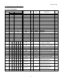
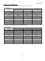
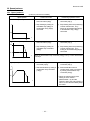
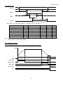
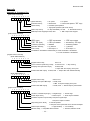
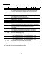
1
DA70133-1/5E Pulse Control LSI With Sequencing Function for Stepper Motors PCD4600 Series PCD4611 PCD4621 PCD4641 User’s Manual Nippon Pulse Motor, Co., Ltd. DA70133-1/5E [Preface] Thank you for considering our pulse control LSI, the "PCD4600 series." Before using the product, read this manual to become familiar with the product. Please note that the section "Handling precautions" which includes details about mounting this LSI, can be found at the end of this manual. [Cautions] (1) Copying all or any part of this manual without written approval is prohibited. (2) The specifications of this LSI may be changed to improve performance or quality without prior notice. (3) Although this manual was produced with the utmost care, if you find any points that are unclear, wrong, or have inadequate descriptions, please let us know. (4) We are not responsible for any results that occur from using this LSI, regardless of item (3) above. (5) If you use it in any device that may require high quality and reliability, or where faults or malfunctions may directly affect human survival or injure humans, such as in nuclear power control devices, aviation devices or spacecraft, traffic signals, fire control, or various types of safety devices, we will not be liable for any problem that occurs, even if it was directly caused by the LSI. Customers must provide their own safety measures to ensure appropriate performance in all circumstances. (5) This LSI is designed for use in commercial apparatus. 高い品質、信頼性が要求され、その故障や誤動作が直接人命を脅かしたり、人体に危険を Descriptions of indicators that are used in this manual 及ぼす恐れのある装置(原子力制御、航空宇宙機、交通信号、燃料制御、各種安全装置な 1 ど)に使用される際にはご注意ください。 When describing the bits in registers, "n" refers to a bit position. "0" refers to a bit position and means that it is prohibited to write any other than "0" and this bit will always return "0" when it is read. A specified bit of a specified register is referred to as (register name).(bit name). (ex. RMD.MSDE) 2 Unless otherwise described, time description affected by the reference clock frequency discussed in this manual is in the case of CLK=4.9152 MHz. 3 4 The "x" "y" "z" and "u" of terminal names refer to X axis, Y axis, Z axis and U axis, respectively. ____ Terminals with a bar above the name (ex. RST ) use negative logic. _____ Example: TOUT means that TOUT terminal uses negative logic. DA70133-1/5E Table of Contents 1. OUTLINE AND FEATURES ................................................................................................................................ 1 1-1. Outline ....................................................................................................................................... 1 1-2. Feature ...................................................................................................................................... 1 2. SPECIFICATIONS ............................................................................................................................................... 2 3. TERMINAL ASSIGNMENT DIAGRAMS ............................................................................................................. 3 3-1. Terminal assignment diagram of PCD4611 (Top View) .............................................................. 3 3-2. Terminal assignment diagram of PCD4621 (Top View) .............................................................. 4 3-3. Terminal assignment diagram of PCD4641 (Top View) .............................................................. 5 4. TERMINAL FUNCTION DESCRIPTION ............................................................................................................. 6 4-1. A list of terminals ...................................................................................................................... 6 4-2. Functions of terminals .............................................................................................................. 7 4-2-1. CLK ........................................................................................................................................................7 ____ 4-2-2. RST .......................................................................................................................................................7 ___ 4-2-3. CS .........................................................................................................................................................7 ___ 4-2-4. WR.........................................................................................................................................................7 ___ 4-2-5. RD .........................................................................................................................................................7 4-2-6. A0, A1, A2, A3 ........................................................................................................................................8 4-2-7. D0 to D7 .................................................................................................................................................8 ____ 4-2-8. INT .......................................................................................................................................................8 ____ 4-2-9. WRQ ......................................................................................................................................................8 __ 4-2-10. U /B .....................................................................................................................................................8 __ 4-2-11. F /H .....................................................................................................................................................8 ____ 4-2-12. STA .....................................................................................................................................................8 ____ 4-2-13. STP .....................................................................................................................................................9 ____ 4-2-14. ORG ....................................................................................................................................................9 ____ ____ 4-2-15. +EL , -EL ..........................................................................................................................................9 ____ ____ 4-2-16. +SD , -SD ..........................................................................................................................................9 4-2-17. ø 1 / P1, ø 2 / P2, ø 3 / P3, ø 4 / P4 .....................................................................................................9 4-2-18. +PO /PLS, -PO/DIR............................................................................................................................10 ____ 4-2-19. BSY ...................................................................................................................................................10 4-2-20. OTS ....................................................................................................................................................10 4-2-21. VDD, GND ..........................................................................................................................................10 4-2-22. (Open) ................................................................................................................................................10 5. BLOCK DIAGRAM ............................................................................................................................................ 11 6. CPU INTERFACE .............................................................................................................................................. 12 6-1. Precaution for designing hardware ......................................................................................... 12 6-1-1. Printed board design .........................................................................................................................12 6-1-2. Unused terminal .................................................................................................................................12 6-1-3. 5 V tolerant ..........................................................................................................................................12 6-1-4. General-purpose input / output ports (ø1 / P1 to ø4 / P4) ...............................................................12 6-1-5. Interrupt processing ..........................................................................................................................12 6-2. Examples of CPU interfaces .................................................................................................... 13 6-3. Address map ........................................................................................................................... 14 6-3-1. Address map of PCD4611 ..................................................................................................................14 6-3-2. Address map of PCD4621 ..................................................................................................................14 6-3-3. Address map of PCD4641 ..................................................................................................................14 6-4. Description of map details ...................................................................................................... 15 - C1 - DA70133-1/5E 6-4-1. Command buffer (COMBF) ................................................................................................................15 6-4-2. Main status (MSTS) ............................................................................................................................15 6-4-3. Register WR buffer (RegWBF)...........................................................................................................15 6-4-4. Register RD buffer (RegRBF) ............................................................................................................15 6-5. Write and read procedures ...................................................................................................... 16 6-5-1. Procedure to write to register ...........................................................................................................16 6-5-2. Procedure to read out register ..........................................................................................................16 6-5-3. Procedure to write start mode command, control mode command and output mode command ........................................................................................................................................................................16 6-5-4. Procedure to write a start command ................................................................................................17 7. COMMAND ........................................................................................................................................................ 18 7-1. Start mode command .............................................................................................................. 19 7-2. Control mode command .......................................................................................................... 20 7-3. Register select command ........................................................................................................ 21 7-4. Output mode command ........................................................................................................... 21 8. REGISTER ACCESS IN COMPATIBLE MODE ................................................................................................ 22 8-1. List of register ......................................................................................................................... 22 8-2. Register in the PCD46x1 mode ................................................................................................ 23 8-2-1. RMV register .......................................................................................................................................24 8-2-2. RFL register ........................................................................................................................................24 8-2-3. RFHregister .........................................................................................................................................25 8-2-4. RUD register .......................................................................................................................................25 8-2-5. RMG register .......................................................................................................................................25 8-2-6. RDP register ........................................................................................................................................26 8-2-7. RSPD monitor, RIDL register .............................................................................................................27 8-2-8. RIDC monitor, RENV register ............................................................................................................27 8-2-9. RCUN register .....................................................................................................................................29 8-2-10. RSTS monitor ...................................................................................................................................30 8-2-11. RIOP register .....................................................................................................................................30 8-3. Register in PCD45x1 mode ...................................................................................................... 32 8-3-1. RMV register .......................................................................................................................................32 8-3-2. RFL register ........................................................................................................................................33 8-3-3. RFH register ........................................................................................................................................33 8-3-4. RUD register .......................................................................................................................................33 8-3-5. RMG register .......................................................................................................................................33 8-3-6. RENV monitor, RDP register..............................................................................................................34 8-3-7. RSPD monitor, RIDL register .............................................................................................................34 8-3-8. RENV register, RIDC monitor, RSTS monitor...................................................................................34 8-4. Registers in PCD4500 mode .................................................................................................... 35 8-4-1. RMV register .......................................................................................................................................35 8-4-2. RSTS monitor .....................................................................................................................................35 9. OPERATION MODE .......................................................................................................................................... 36 9-1. Continuous mode .................................................................................................................... 36 9-2. Origin return mode .................................................................................................................. 37 9-3. Positioning mode .................................................................................................................... 40 9-4. Timer mode ............................................................................................................................. 41 9-4-1. Procedure example to use this mode as a 100 ms timer ................................................................41 10. SPEED PATTERNS ......................................................................................................................................... 42 10-1. Speed patterns ...................................................................................................................... 42 10-2. Speet pattern settings ........................................................................................................... 43 10-3. Setting example of acceleration / deceleration pattern ......................................................... 45 - C2 - DA70133-1/5E 10-4. Changing speed patterns in operation .................................................................................. 46 11. FUNCTION DESCRIPTION ............................................................................................................................. 48 11-1 Reset....................................................................................................................................... 48 11-2. Idling pulse output ................................................................................................................ 48 11-3. External start control ............................................................................................................. 49 11-4. External stop control ............................................................................................................. 49 11-5. Output pulse mode ................................................................................................................ 49 11-6. Excitation sequence output ................................................................................................... 50 11-7. External mechanical input control ........................................................................................ 51 ___ 11-8. Interrupt request signal ( INT) output ..................................................................................... 52 11-9. General-purpose port ............................................................................................................ 53 11-9-1. Terminal OTS.....................................................................................................................................53 _ _ 11-9-2. Terminals U/B, F/H ..........................................................................................................................53 11-9-3. Terminals ø1 / P1, ø2 / P2, ø3 / P3, ø4 / P4 ......................................................................................54 12. ELECTRICAL CHARACTERISTICS ............................................................................................................... 55 12-1. Absolute maximum rating ..................................................................................................... 55 12-2. Recommended operating conditions .................................................................................... 55 12-3. DC characteristics (in recommended operating conditions) ................................................ 55 12-4. AC characteristics ................................................................................................................. 56 12-4-1. Reference clock ................................................................................................................................56 12-4-2. Reset cycle ........................................................................................................................................56 12-4-3. Read cycle .........................................................................................................................................56 12-4-4. Write cycle.........................................................................................................................................57 12-5. Operation timing.................................................................................................................... 57 12-5-1. Accelerating / decelerating operation timing (Positioning operation) ........................................57 12-5-2. Start timing ........................................................................................................................................58 12-5-3. Stop timing ........................................................................................................................................58 12-5-4. Pulse output, sequence output timing ...........................................................................................59 12-5-5. General-purpose port output timing ...............................................................................................59 13. EXTERNAL DIMENSIONS .............................................................................................................................. 60 13-1. External dimensions of PCD4611 (48 pin QFP) ..................................................................... 60 13-2. External dimensions of PCD4621 (64 pin QFP) ..................................................................... 61 13-3. External dimensions of PCD4641 (100 pin QFP) ................................................................... 62 14. HANDLING PRECAUTIONS ........................................................................................................................... 63 14-1. Hardware design precautions ............................................................................................... 63 14-2. Software design precautions................................................................................................. 63 14-3. Mechanical precaution .......................................................................................................... 63 14-4. Precautions for transporting and storing LSIs ..................................................................... 64 14-5. Precautions for mounting ..................................................................................................... 64 14-6. Other precautions ................................................................................................................. 65 APPENDIX............................................................................................................................................................. 66 Appendix A. Command list............................................................................................................. 66 Appendix B. Register list ............................................................................................................... 67 Appendix C. Status list................................................................................................................... 68 Appendix D. Differences from PCD45x1 ........................................................................................ 69 - C3 - DA70133-1/5E 1. Outline and features 1-1. Outline PCD4611 / 4621 / 4641 are pulse control LSIs with phase sequence control for 2-phase stepper motor. Using these LSIs and ICs for stepping drive allows you to construct stepper motor control system. Inputting data and commands from CPU allows you to control speed and positioning, etc. Using output pulse signal drive can control motor drive of pulse train input type. 1-2. Feature - 3.3 V single power source (Input and output terminals have 5 V tolerance feature.) - Maximum output frequency 4.91 Mpps (Reference clock : 9.8304 MHz (Maximum frequency), speed magnification : 300x) - Wait control is added for interface with CPU. - Excitation sequencing output for 2-phase stepper motor. - Four terminals for sequence output can be used as general-purpose I/O terminals. - Pulse train output (CW and CCW pulse, pulse and direction signal.) - Linear and S-curve acceleration / deceleration control. - External start / stop control - Positioning operation / origin return operation/ continuous operation / timer operation - Idling pulse output - 24-bit current position counter - Automatic setting for a ramping-down point.___ ____ ____ ____ Selection of stop method by ORG, +EL , -EL, STP signals. (Immediate stop / deceleration stop) Available in single axis (PCD4611), 2-axis (PCD4621), and 4-axis (PCD4641) 2.46 Mpps (Reference clock : 4.9152 MHz (Standard frequency), speed magnification : 300x) Note: If control software for PCD4511/ PCD4521 / PCD4541 is used for PCD 4611/PCD4621/PCD4641, slight modification is needed. - 1 - DA70133-1/5E 2. Specifications Item Standard Power source 3.0 to 3.6 V Reference clock 4.9152 MHz standard (10 MHz max) Number of control axes PCD4611 : one PCD4621 : two PCD4641 : four 0 to 16,777,215 pulses (24 bits) Positioning control range Speed setting step range 1 to 8,191 steps (13 bits) Recommended speed magnification 1x to 300x (when using reference clock :4.9152 MHz) When 1x, 1 to 8,191 pps range When 2x, 2 to 16,382 pps When 5x, 5 to 40,955 pps When 10x, 10 to 81,910 pps When 20x, 20 to 163,820 pps When 50x, 50 to 409,550 pps When 100x, 100 to 819,100 pps When 200x, 200 to 1,638,200 pps When 300x, 300 to 2,457,300 pps Number of registers for setting the Two per axis (FL and FH) speed Ramping-down point setting range 0 to 16,777,215 (24 bits per axis) Ramping-down point setting method Manual setting or automatic setting Acceleration / deceleration rate Linear and S-curve acceleration / deceleration setting range Acceleration / deceleration rate 1 to 65,535 (16 bits per axis) setting range Current position counter 24-bit UP / DOWN counter one circuit / axis Mechanical sensor input The following signals are input per axis  ̄  ̄ ̄ (Origin) ORG  ̄ ̄ ,  ̄  ̄ (End limit) +EL -EL  ̄  ̄ ̄,  ̄  ̄ ̄ (Ramping-down) +SD -SD Typical operations - Continuous operation - Positioning operation Typical functions - Origin return operation - Timer operation - Immediate stop and decelerating stop - Speed change - External start and external stop function - Idling pulse output function - Excitation sequencing output for 2-phase stepper motor - 4-bit general-purpose input and output ports (They also can be used as sequence output) Ambient operating temperature Storage temperature Package Chip design -40 to +85 °C -65 to +150 °C PCD4611: 48 pin QFP PCD4621: 64 pin QFP PCD4641: 100 pin QFP C-MOS - 2 - (Mold section :7.0× 7.0 mm) (Mold section :10.0×10.0 mm) (Mold section :14.0×14.0 mm) DA70133-1/5E 3. Terminal assignment diagrams U/B ___ STP ___ STA ø 4/P4 ø 3/P3 ø 2/P2 ø 1/P1 VDD _ F/H _ CLK 36 35 34 33 32 31 30 29 28 27 26 25 24 23 22 21 20 19 18 17 16 15 14 13 1 2 3 4 5 6 7 8 9 10 11 12 GND GND GND D5 D6 D7 D2 D3 D4 PCD4611 D0 D1 INT _____ WRQ GND ____ RST ___ CS ___ WR ___ RD VDD A1 A0 GND 37 38 39 40 41 42 43 44 45 46 47 48 VDD VDD ___ GND OTS 3-1. Terminal assignment diagram of PCD4611 (Top View) - 3 - GND (Open) ___ BSY +PO/PLS -PO/DIR VDD ____ ORG ___ +EL ___ -EL ___ +SD ___ -SD GND DA70133-1/5E ø3 X/P3X ø2X/P2X +POX/PLSX ø4X/P4X BSYX -POX/DIRX VDD OTS ___X ø 1Y/P1Y 28 27 PCD4621 26 25 24 23 22 21 - 4 - GND D0 D1 D2 D3 GND A2 20 19 18 17 1 2 3 4 5 6 7 8 9 10 11 12 13 14 15 16 WR ___ RD A0 A1 -ELY ___ +SD ___Y -SDY VDD CLK GND GND GND GND 48 47 46 45 44 43 42 41 40 39 38 37 36 35 34 33 32 31 30 29 RST ___ CS ___ STA ___ Y STP ___ Y ORG ___ Y +EL ___Y 48 48 48 48 48 48 48 48 48 48 48 48 48 48 48 48 ___ INT ____ WRQ VDD ____ GND _ U/B _ Y F/H ___ Y +POY/PLSY ø 4Y/P4Y ø 3Y/P3Y ø 2Y/P2Y OTS ___Y BSYY -POY/DIRY 3-2. Terminal assignment diagram of PCD4621 (Top View) ø 1 X /P1 X GND ___ -SD ___X +SDX ___ -EL ___X +EL ___X ORG ___ X STP ___ X STA _ X F/H _ X U/BX VDD D7 D6 D5 D4 DA70133-1/5E +POY/PLSY BSYZ GND OTSY -POY/DIRY ø 3Z/P3Z ø 2Z/P2Z ø 1Z/P1Z ___ VDD OTSZ -POZ/DIRZ +POZ/PLSZ ø 4Z/P4Z F/H _ Z U/BZ +EL ___Z ORG ___ Z STP ___ Z STAZ _ 48 47 46 45 78 79 80 81 82 83 84 85 86 44 43 42 41 40 87 39 38 88 89 37 90 36 91 35 92 34 33 93 94 32 31 95 96 30 97 29 28 98 99 27 100 26 1 2 3 4 5 6 7 8 9 10 11 12 13 14 15 16 17 18 19 20 21 22 23 24 25 - 5 - OTSX +POX/PLSX -POX/DIRX BSYX ø 1X/P1X ø 2X/P2X ø 3X/P3X ø 4X/P4X D5 D6 D7 6 VDD ___ D0 D1 D2 D3 D4 WRQ GND PCD4641 A3 VDD ___ INT ____ -SDU GND ___ BSYU ø 1U/P1U ø 2U/P2U ø 3U/P3U ø 4U/P4U +POU/PLSU -POU/DIRU OTSU VDD CLK GND GND GND GND ____ RST ___ CS ___ RD ___ WR 75 74 73 72 71 70 69 68 67 66 65 64 63 62 61 60 59 58 57 56 55 54 53 52 51 76 50 49 77 A0 A1 A2 ___ STPU ___ ORG ___U +EL ___U -ELU ___ +SD ___U +SD ___ Z -ELZ ___ ___ STA _ U F/H _ U U/B ___U -SD ___Z 3-3. Terminal assignment diagram of PCD4641 (Top View) ø 4Y/P4Y ø 3Y/P3Y ø 2Y/P2Y ø 1Y/P1Y ___ BSYY VDD ___ ___ Y -SD +SDY ___ -ELY ___ +EL ___Y ORG ___ Y STP ___ Y STA _ Y F/H _ Y U/B ___Y -SD ___X +SDX ___ -EL ___X +EL ___X ORG ___ X STP ___ X STA _ X F/H _ X U/BX GND DA70133-1/5E 4. Terminal function description 4-1. A list of terminals Terminal number PCD4611 PCD4621 X 36 41 42 43 44 47 46 2 3 4 5 6 7 8 9 38 39 Y 60 4 5 6 7 8 9 10 12 13 14 15 17 18 19 20 1 2 PCD4641 X Y Z Terminal name I/O Logic CLK ____ RST ___ CS ___ WR ___ RD A0 A1 A2 A3 D0 D1 D2 D3 D4 D5 D6 D7 ___ INT ____ WRQ _ U/B I I% I I I I I I I I/O I/O I/O I/O I/O I/O I/O I/O O* O Negative Negative Negative Negative Positive Positive Positive Positive Positive Positive Positive Positive Positive Positive Positive Positive Negative Negative - Description U 92 97 98 100 99 1 2 3 4 9 10 11 12 13 14 15 16 6 7 27 22 50 27 36 64 73 28 23 51 28 37 65 74 25 24 52 29 38 66 75 26 25 53 30 39 67 76 18 26 54 31 40 68 77 5V tole -rant I% Negative Reference clock Reset signal Chip select signal Write signal Read signal Address bus 0 (LSB) Address bus 1 Address bus 2 Address bus 3 Data bus 0 (LSB) Data bus 1 Data bus 2 Data bus 3 Data bus 4 Data bus 5 Data bus 6 Data bus 7 Interrupt request signal Wait request signal Select excitation method (L: unipolar / H: bipolar) Select excitation sequence (L: 2-2 phase / H: 1-2 phase) External start signal I% Negative External stop signal O I% Negative Origin position switch signal O I% Negative (+) end limit switch signal O I% Negative (-) end limit switch signal O I% Negative (+) deceleration switch signal O I% Negative (-) deceleration switch signal O Positive 1st phase excitation signal / general-purpose I/O 1 2nd phase excitation signal I% 17 27 55 32 41 69 78 16 28 56 33 42 70 79 15 29 57 34 43 71 80 14 30 58 35 44 72 81 _ F/H ____ STA ____ STP ____ ORG ____ +EL ___ -EL ____ +SD ___ -SD 30 32 41 19 47 56 84 ø1 / P1 I/O% 31 33 42 20 48 57 85 ø2 / P2 I/O% 32 34 43 21 49 58 86 ø3 / P3 I/O% 33 35 44 22 50 59 87 ø4 / P4 I/O% 21 36 45 23 51 60 88 +PO / PLS O I% - 6 - - Positive / general-purpose I/O 2 Positive 3rd phase excitation signal / general-purpose I/O 3 Positive 4th phase excitation signal / general-purpose I/O 4 Negative # (+) pulse / common pulse signal O O O O O O O O O O O O O O O O O O O O O O O O O O O DA70133-1/5E Terminal number PCD461 1 PCD462 1 PCD4641 Terminal name I/O Logic O Negative # O O X Y X Y Z U 20 37 46 24 52 61 89 22 38 47 18 46 55 83 -PO / DIR ____ BSY 34 1,19, 29,37, 45 10,11, 12,13, 24,35, 40,48 39 48 25 53 62 90 OTS 23 3,21, 40,59 5,17,45,63,91 11,16, 31,49, 61,62 63,64 8,26,54,82, 93,94,95,96 GND - - (Open) VDD Description 5V tole -rant (-) pulse / direction signal O Negative Running signal O Negative General-purpose output signal Power input +3.3 V(3.0 to 3.6 V) input O Power GND O Output terminal for delivery inspection (always open) X Notes: - ‘%’ in the I/O column means that a pull-up register is integrated and ‘*’ means open drain. - ‘#’ in the logic column is a terminal that the logic is changeable and the logic described here is a default. 4-2. Functions of terminals 4-2-1. CLK This is an input terminal of the reference clock. Ordinary, clock from 4.9152 MHz crystal oscillator (3.3 V) is input. ____ The accuracy of reference clock affects accuracy of output pulse. It also affects start timing, input sensitivity of +EL , ___ ____ ____ ____ -EL, ORG, STA , STP signals and timing of writing and reading. ____ 4-2-2. RST This is an input terminal for a reset signal. By making this terminal LOW level and inputting 3 or more clocks of reference clock, the internal circuit of PCD46x1 is reset. About the default setting after reset, see “11-1. Reset”. ___ 4-2-3. CS This is an input terminal for a chip select signal. ___ ___ By making this terminal LOW level, a RD signal and a WR signal are enabled and reading and writing operation from CPU becomes available. ___ 4-2-4. WR This is an input terminal for a write signal. ___ When CS terminal is LOW level, the status of data bus (D0 to D7) is written to the internal at the timing when this signal changes from LOW level to HIGH level. ___ 4-2-5. RD This is an input terminal for a read signal. ___ By making this terminal LOW level when the CS terminal is LOW level, the contents of the main status and the register are output to the data bus (D0 to D7). - 7 - DA70133-1/5E 4-2-6. A0, A1, A2, A3 These are input terminals of address signals. The LSI uses A0 and A1 terminals to assign access address to the upper, middle and lower of the Command buffer (COMBF), the Register RD buffer (RegRBF) and the Register WR buffer (RegWBF). Normally, the LSI connects to the lowest bit of CPU address bus. On the PCD4621 and 4641, terminals A2 and A3 are used to select axes to control. The A0 terminal is the lowest bit. 4-2-7. D0 to D7 These are input and output terminals for the tri-state data bus. The D0 terminal is the lower bit (LSB) and the D7 terminal is the upper bit (MSB). ____ 4-2-8. INT This is an output terminal for sending an interrupt request signal to a CPU. This terminal will go LOW when an interrupt condition occurs. With reset by a command of interrupt condition setting, this terminal returns to HIGH level. This terminal can also be masked. ___ By setting the Start mode command, the LSI can output an INT signal when a motor stops. Using this terminal, you ____ can call for an interrupt when positioning operation is complete, or when operation is stopped by an ORG signal, ____ ___ ____ +EL or -EL signal, or STP signal. An interrupt can also be requested by an immediate stop command or a deceleration stop command. ___ Using the setting of Register select command, an INT request signal can be output when a motor starts deceleration by a ramping-down point setting or when a motor starts by an external signal. ___ When you use several PCD4611 / PCD4621 / PCD4641s, each INT terminal of each LSI can be connected in a wired OR configuration. Use an external pull up resistor (5 to 10 K ohms) to stabilize HIGH level though a pull-up resistor is built in for prevention from static electricity. ____ 4-2-9. WRQ This terminal outputs a wait request signal for CPU. While this terminal is LOW level, extend access cycle of CPU. ____ When WRQ is not used, ensure access interval by software. For the detail about access interval, see “6-5. Write / read procedures”. __ 4-2-10. U /B This is a terminal for selecting excitation method. Select unipolar excitation sequencing with a LOW or bipolar excitation sequencing with a HIGH on this terminal. ____ The setting of this terminal is latched at the cancel of reset. Therefore, input a RST signal after setting change. About difference of sequence by excitation method, see “11-6. Excitation sequence output”. When excitation sequence output is not used, this terminal can be used as a general-purpose input terminal. __ 4-2-11. F /H This is a terminal for selecting excitation sequence. 2-2 phase and 1-2 phases are typical excitation sequences for 2-phase stepper motors. Select sequence using this terminal. Select 2-2 phase excitation with a LOW and 1-2 phase excitation sequencing with a HIGH. For details about the sequence for reading this terminal, see "11-6. Excitation sequence output." When excitation sequence output is not used, this terminal can be used as a general-purpose input terminal. ____ 4-2-12. STA This is an input terminal for an external start signal. - 8 - DA70133-1/5E When a Hold start command is entered using a Start mode command, the motor starts on the falling edge of this ____ STA . A signal shorter than 4 cycles of the reference clock is not accepted because of a noise filter. ____ 4-2-13. STP This is an input terminal for a forced stop signal. ____ When the STP signal goes LOW, regardless of the direction of the motor, the motor will stop immediately or decelerate and stop. Even if this signal goes HIGH again, the LSI will not let the motor start. ____ If the STP signal is already LOW when a Start mode command is written, the LSI will not let the motor start. You can select between immediate stop and deceleration stop by RENV.SPDS. A noise filter can be applied by Output mode command.OCM4. ____ The maximum time from a signal input to stop ( BSY=H) is FL pulse cycle. ____ 4-2-14. ORG This is an input terminal for the origin position sensor signal. ____ When ORG signal control is enable (origin return operation) with Control mode command.CCM0=1 and when this signal goes LOW, the motor will stop immediately or decelerate and stop. Even if this signal goes HIGH again, the LSI does not start the motor. ____ When ORG signal control is disabled with Control mode command.CCM0=0 and pulse output is masked with Output mode command.OCM1=1 (in timer mode), this signal is disabled. A noise filter can be applied by Output mode command.OCM4. ____ The maximum time from a signal input to stop ( BSY=H) is FL pulse cycle. ____ ____ 4-2-15. +EL , -EL These are input terminals for end limit switch signals. __ When an EL signal which has the same direction as the operation goes LOW, the motor will stop immediately or decelerate and stop. The LSI will not let the motor restart, even when this signal goes HIGH again. __ If the EL signal of the operation direction is already LOW when a Start mode command is written, the LSI will not let the motor start. When pulse output is masked with Output mode command.OCM1=1 (in timer mode), this signal is disabled. A noise filter can be applied by Output mode command.OCM4. ____ The maximum time from a signal input to stop ( BSY=H) is FL pulse cycle. ____ ____ 4-2-16. +SD , -SD These are input terminals for deceleration switch signals. ____ ___ When +SD and -SD signals are enabled with Control mode command.CCM1=1 and when this signal which has the same direction as the operation goes LOW, the motor will stop immediately or decelerate and stop. Then, when this signal returns HIGH, the motor will accelerate again. 4-2-17. ø 1 / P1, ø 2 / P2, ø 3 / P3, ø 4 / P4 These are output terminals of excitation sequence signals for stepper motors. When sequence output is unnecessary, you can use these terminals as general-purpose input/output terminals (P1 to P4) with RENV.IOPM=1. If you use these as general-purpose input/output terminals, you can select input or output every terminal by RENV.IPM1 to IPM4. If you use these as excitation sequence output terminals, sequence signals are switched with synchronized with the output pulses. _ Using the F/H terminals, you can select between 1-2 phase and 2-2 phase excitation sequencing. _ Using the U/B terminals, you can select between unipolar and bipolar excitation sequencing. When pulse output control is masked with Output mode command.OCM1=1, the excitation sequencing cannot be - 9 - DA70133-1/5E changed. Excitation sequence output can be masked (all terminals ø 1 to 4 are LOW level) with Output mode command.OCM2=1 4-2-18. +PO /PLS, -PO/DIR These are output terminals of pulse train for motor driving. These terminals have two modes: two pulse mode to output (+) and (-) direction pulse train and common pulse mode to output pulse trains and direction signals. The mode of pulse output is set by RENV.PMD. Output logic is set by Output mode command.OCM0. The direction of motor’s operation is set by Control mode command.CCM3. The duty of output pulse train is approximately 50%. ____ 4-2-19. BSY This is a terminal to monitor operation condition. This terminal goes LOW level when this LSI operates. It is used to check operation condition and to control current reduction of motor drive when a motor stops. 4-2-20. OTS This is a general-purpose output terminal. This terminal can be used as an excitation ON/OFF control signal for a motor driver IC. This terminal becomes HIGH level with Control mode command.CCM4=1 and becomes LOW level with Control mode command.CCM4=0. 4-2-21. VDD, GND These are power supply terminals. Supply +3.0 to 3.6 V to the VDD terminals. Make sure to connect all of the power supply terminals. 4-2-22. (Open) This is an output terminal for testing. Only PCD4611 has this terminal. Be sure to make it open. - 10 - DA70133-1/5E 5. Block Diagram There are the same number of blocks surrounded by a dotted line as the number of axes. CLK +3.3 V GND RFL register RFH register RUD register RMG register RDP register RIDL register RENV register RCUN register RSTS register RIDC register RIOP register RSPD register  ̄ ̄ ̄ CS Note A0 to A3 CPU I/F  ̄ ̄ ̄ ̄ ̄ WRQ D0 to D7  ̄ ̄ ̄ ̄ STA  ̄ ̄ ̄ ̄ STP Degital Filter  ̄ ̄ ̄ -SD  ̄ ̄ ̄ ̄ ORG  ̄ ̄ ̄ INT Accel /decel control circuit [linear / S-curve](RUD) 2-phase Excitation Sequence generation circuit Comparator Φ1 Φ2 Φ3 Φ4  ̄ ̄ U /B  ̄ /H F Idling pulse (RIDL) Positioning control couner (RMV) +PO/PLS -PO/DIR Current position counter (RCUN) Ramping-down point (RDP) Command buffer  ̄ ̄ ̄ +EL  ̄ ̄ ̄ -EL  ̄ ̄ ̄ +SD OTS, P1to P4 control circuit Variable division circuit (RFL, RFH) RMV register  ̄ ̄ ̄ ̄ RST  ̄ ̄ ̄ WR Pulse output Internal register VDD  ̄ ̄ ̄ RD Magnification rate division circuit (RMG) INT Output control Control circuit  ̄ ̄ ̄ ̄ BSY General -purpose port control (RIOP) Note. Address signal input terminals vary according to the models. PCD4611: A0 to A1, PCD4621: A0 to A2, PCD4641: A0 to A3 - 11 - DA70133-1/5E 6. CPU interface 6-1. Precaution for designing hardware 6-1-1. Printed board design - To stabilize operation, we recommend 4-layer printed board with a 3.3 V power layer and a GND layer. - We recommend that about 0.1 uF condenser is put between 3.3 V and GND near each side of this LSI. 6-1-2. Unused terminal - Unused input terminals should be pulled up to 3.3 V with a 5 K to 10 K ohm resistor or connected to 3.3 V. - Unused bi-directional terminals should be pulled up to 3.3 V with a 5K to 10K ohm resistor. - Unused output terminals should be open (no connection). 6-1-3. 5 V tolerant All signal terminals of this LSI have 5 V tolerant function. Please note the followings. - Even though an output terminal is pulled up to 5 V, the voltage does not become more than 3.3 V. If more than 3.3 V of voltage is needed as HIGH level, level conversion circuit is necessary externally. - When more than 3.3 V of voltage is input to an input (input / output) terminal, leakage occurs to 3.3 V through an internal pull-up resistor (40K to 240K ohm) and input current increases. - There is no diode for protection from overvoltage between terminals and 3.3 V in the input circuit. When there is possibility that more than absolute maximum rating voltage is input, you should add protection circuit externally. 6-1-4. General-purpose input / output ports (ø1 / P1 to ø4 / P4) General-purpose terminals are output terminals for sequence signals at default to be compatible with PCD45x1. If you use these as input ports, please make sure that you insert a series resistor to prevent from short circuit with external output circuit. If you use these as output ports, a series resistor is unnecessary. However, please note that the default condition is output level of sequence signals. PCD46x1 P1(IN) Resistor More than 1 k ohm is needed to prevent from breakage of PCD46x1. To prevent from breakage of an external circuit, select a value of resistors so as that the current is less than the maximum output current of the external circuit. 6-1-5. Interrupt processing When an interrupt occurs during write / read processing to registers and access to registers is made in interrupt routine, the content of the register WR (RD) buffer is changed. Therefore, hold an interrupt processing during write / read processing to registers. - 12 - DA70133-1/5E 6-2. Examples of CPU interfaces R5F562N (Renesas RX600) +3.3 V VCC EXTAL PCD4641 (NPM) VDD 12 MHz 4.9152 MHz CLK A3 ___ CS A3 A2 A2 A1 A1 A0 A0 CSn# ___ RD ___ WR ____ WRQ ___ INT RD# WR# WAIT# IRQn D7 D7 D6 D6 D5 D5 D4 D4 D3 D3 D2 D2 D1 D1 D0 D0 ____ RST GND RES# VSS ______ Reset Note1. When PCD4621 is used, connection to the A3 terminal signal is unnecessary. Note 2. When PCD4611 is used, connection to the A3 and A2 terminal signals is unnecessary. Note 3. Set as follows with CPU software. - Select “8-bit bus space" for external bus width. - External wait is permitted. - Select “Low” for IRQ detection. - 13 - DA70133-1/5E 6-3. Address map Four address areas are occupied per axis in PCD46x1. (1 byte / address) Therefore, 4 address areas in PCD4611, 8 address areas in PCD4621, 16 address areas in PCD4641 are occupied. COMBF : Command buffer MSTS : Main status RegWBF : Buffer for write registers RegRBF : Buffer for read registers 6-3-1. Address map of PCD4611 A1 to A0 Write Read 00 Write to COMBF Read MSTS 01 Write to RegWBF (7 to 0) Read out RegRBF (7 to 0) 10 Write to RegWBF (15 to 8) Read out RegRBF (15 to 8) 11 Write to RegWBF (23 to 16) Read out RegRBF (23 to 16) 6-3-2. Address map of PCD4621 A2 to A0 Axis Write Read 000 X Write to COMBF_x Read MSTS_x 001 X Write to RegWBF_x (7 to 0) Read out RegRBF_x (7 to 0) 010 X Write to RegWBF_x (15 to 8) Read out RegRBF_x (15 to 8) 011 X Write to RegWBF_x (23 to 16) Read out RegRBF_x (23 to 16) 100 Y Write to COMBF_y Read MSTS_y 101 Y Write to RegWBF_y (7 to 0) Read out RegRBF_y (7 to 0) 110 Y Write to RegWBF_y (15 to 8) Read out RegRBF_y (15 to 8) 111 Y Write to RegWBF_y (23 to 16) Read out RegRBF_y (23 to 16) 6-3-3. Address map of PCD4641 A3 to A0 Axis Write Read 0000 X Write to COMBF_x Read MSTS_x 0001 X Write to RegWBF_x (7 to 0) Read out RegRBF_x (7 to 0) 0010 X Write to RegWBF_x (15 to 8) Read out RegRBF_x (15 to 8) 0011 X Write to RegWBF_x (23 to 16) Read out RegRBF_x (23 to 16) 0100 Y Write to COMBF_y Read MSTS_y 0101 Y Write to RegWBF_y (7 to 0) Read out RegRBF_y (7 to 0) 0110 Y Write to RegWBF_y (15 to 8) Read out RegRBF_y (15 to 8) 0111 Y Write to RegWBF_y (23 to 16) Read out RegRBF_y (23 to 16) 1000 Z Write to COMBF_z Read MSTS_z 1001 Z Write to RegWBF_z (7 to 0) Read out RegRBF_z (7 to 0) 1010 Z Write to RegWBF_z (15 to 8) Read out RegRBF_z (15 to 8) 1011 Z Write to RegWBF_z (23 to 16) Read out RegRBF_z (23 to 16) 1100 U Write to COMBF_u Read MSTS_u 1101 U Write to RegWBF_u (7 to 0) Read out RegRBF_u (7 to 0) 1110 U Write to RegWBF_u (15 to 8) Read out RegRBF_u (15 to 8) 1111 U Write to RegWBF_u (23 to 16) Read out RegRBF_u (23 to 16) - 14 - DA70133-1/5E 6-4. Description of map details 6-4-1. Command buffer (COMBF) This is a buffer to write a start command, Control mode command, Register select command and Output mode command. A written command is determined by the upper 2 bits and memorized in separate command areas. D7 to D6 Command (D5 to D0) 00 Start mode command 01 Control mode command 10 Register select command 11 Output mode command 6-4-2. Main status (MSTS) Monitor current status of axis. 7 6 5 4 3 2 1 0 FDWN FUP SDP PLSZ BUSY ISTA ISDP ISTP Bit Bit name Contents 0 ISTP Requesting an interrupt by stop (0: ON, 1: OFF) 1 ISDP Requesting an interrupt by ramping-down point (0: ON, 1: OFF) 2 ISTA Requesting an interrupt by external start (0: ON, 1: OFF) 3 BUSY 0: Stopping , 1: Running 4 PLSZ 1: (RMV=0) 5 SDP 1: (RMV ≤ RDP) 6 FUP 1: Accelerating 7 FDWN 1: Decelerating ___ Note. During at least one is ON among ISTP, ISDP and ISTA, the INT terminal goes LOW level. 6-4-3. Register WR buffer (RegWBF) This is a buffer to write all bits to a register at once. When the lower byte is written, all bits are written to a specified register at once. Therefore, please write the upper byte and middle byte, and then write the lower byte last. 6-4-4. Register RD buffer (RegRBF) This is a buffer to read all bits from a register at once. The contents of a specified register are copied to this buffer by writing a register select command. The order to read upper, middle and lower byte is arbitrary. - 15 - DA70133-1/5E 6-5. Write and read procedures In processing to access to registers, processing time is needed to transfer data at the following timing. - In processing to write to registers, shortly after writing to the WR buffer (7 to 0). - In processing to read out registers, shortly after writing a Register select command. 6-5-1. Procedure to write to register 1. Write a Register select command to COMBF. Write a Register select command Though the current register value is copied to the register RD buffer, it is not used. Write the upper data to the RegWBF (23 to 16) Write the middle data to the RegWBF (15 to 8) Write the lower data to the RegWBF (7 to 0) Wait internal processing time (CLK 2 cycles) 2. Write the upper (or middle) data. 3. Write the middle (or upper) data. 4. Write the lower data last. By writing the lower data, data transmission of all bits starts. ____ 5. When the WRQ output is not used, please set not to make a next access during transmission processing time using software. ____ (When the WRQ is used, automatic processing operates.) 6-5-2. Procedure to read out register 1. Write a Register select commandto COMBF. Write a Register select command Wait internal processing time (CLK 2 cycles) Read the upper data from the RegRBF (23 to 16) The current register value is copied to the register RD buffer. ____ 2. Wait a copy processing time (longer than CLK 2 cycles). When the WRQ output is connected to CPU, software processing is unnecessary. Note. It’s duration is CLK 1.5 cycle in PCD 45x1 and CLK 2 cycles in PCD46x1. 3. Read out the buffer for reading from the registers. In this example, the upper, middle and lower data are read in order. Read the middle data from the RegRBF (15 to 8) However, the order to read is arbitrary. Read the lower data from the RegRBF (7 to 0) 6-5-3. Procedure to write start mode command, control mode command and output mode command After writing a command, delay for 1 cycle of CLK occurs until the LSI inside is changed. When you write a start command as a start mode command, the following procedure is needed to process. Start command is a start mode command whose bits 4 and 3 are “10”. There are three start commands: FL constant speed start command, FH constant speed start command and high start command. - 16 - DA70133-1/5E 6-5-4. Procedure to write a start command 1. A dammy command is a command that only the bit 4 of the start command to be Write a dummy command Wait internal processing time (CLK 1 cycle) Write a start command used is changed to “0”.. ____ 2. When the WRQ output is connected to CPU, put waiting time of longer than CLK 1 cycle by software. 3. Write a start command Note. If you write a start command without the above procedure, the Start command may be ignored and it does not initiate starts. With PCD4500, PCD45x1 series, writing a dummy command is unnecessary. Regarding only this procedure, there is no compatibility with software for PCD4500 and PCD45x1 series. If you try to the above procedure for PCD4500 or PCD45x1 series, there is nothing that matters. Example: Procedure to write 15h as a Start command 1. Write 05h as a dummy command 2. Wait for longer than CLK one cycle 3. Write 15h as an original Start command. - 17 - DA70133-1/5E 7. Command Commands to control this LSI are written in the 8-bit command buffer. Witten command is determined by the upper 2 bits and classified in four types and stored separately. Bit 7 and 6 00 01 10 11 Command type Start mode command Command about start / stop such as FL constant speed start, FH constant speed start, high speed (with acceleration / deceleration) start, immediate stop and deceleration stop. Control mode command Command about operation mode such as continuous operation, origin return operation and positioning operation. Register select command Command to select a register when writing to / reading out an internal register. Output mode command Command about setting of input/output signals such as output pulse logic, mask of sequence output, selection of sensor input sensitivity and monitor mode. 1. Writing a Start mode command will make the LSI starts operation. Therefore, write a Control mode command first and set to a register for operation and write an Output mode command. Then, write a Start mode command last. To write a start command, see “6-5-4. Procedure to write a start command”. 2. When a setting value of a Control mode command and an Output mode command that you want to use is the same as the previous one, writing process is unnecessary. 3. Registers other than RMV, when this time value you want to set is the same as the the previous one, writing process is unnecessary. 4. Even if you want to repeat the same feed amount positioning operation, please write feed amount to the RMV register every time. - 18 - DA70133-1/5E 7-1. Start mode command Commands about start / stop. 7 6 5 4 3 2 1 0 0 0 SCM5 SCM4 SCM3 SCM2 SCM1 SCM0 Bit Bit name 0 SCM0 1 SCM1 2 SCM2 4 to 3 5 SCM4 to 3 SCM5 Description Operation speed selection 0: Operates at FL speed (RFL setting speed) 1: Operates at FH speed (RFH setting speed) Hold start 0: Normal start ____ 1: Hold start and start by inputting STA Speed mode selection 0: Constant speed operation 1: High speed (with acceleration / deceleration) start Start / Stop control 01: Request to stop immediately 10: Request to start 11: Request to decelerate and stop ___ INT output control when a motor stops ___ ___ 0: Does not___ output INT when a motor stops. (INT output is reset when a motor stops.) 1: Outputs INT when a motor stops Example of command setting Start mode command Bit 7 to 0 00010000 Hex 10(h) 00110000 30(h) 00010010 12(h) 00110010 00010001 32(h) 11(h) 00010011 13(h) 00010101 15(h) 00010111 00010100 17(h) 14(h) 00011101 1D(h) 00111101 3D(h) 00001000 08(h) 00101000 28(h) 00X11X1X Operation ___ FL constant speed start (INT is disabled while the motor stops) When this command is written during a motor stops, constant speed operation starts at FL speed. When this command is___ written while a motor is running, the speed changes to FL speed immediately. FL constant speed start (INT is enabled while the motor stops.) ___ Hold FL constant speed start (INT is disabled while the motor stops.) ___ Hold FL constant speed start (INT is enabled while the motor stops.) ___ FH constant speed start (INT is disabled while the motor stops.) When this command is written during the motor stops, constant speed operation starts at FH speed. When this command is written ___during the motor stops, the speed change to FH speed immediately. Hold FH constant speed start (INT is disabled while the motor stops.) ___ FH high-speed start (INT is disabled while the motor stops.) When this command is written during the motor stops, operation starts at FL speed and accelerates to FH speed. When this command is written during the motor is running, operation accelerates and the speed changes to FH speed. ___ Hold FH high-speed start (INT is disabled while the motor stops) ___ Deceleration on the way (INT is disabled while the motor stops) When this command is written during the motor is running, operation decelerates and the speed changes to FL speed. (When command is___ written during the motor is running, constant speed operation starts at FL speed.) Decelerate and stop(INT is disabled when the motor stops) When this command is written during the motor is running at FH speed, operation decelerates to FL speed and stops. When this command is written during a motor is running at FL speed, a motor stops immediately. ___ Decelerate and stop (INT is enabled when the motor stops) ___ Stop immediately (INT is disabled when the motor stops) ___ Stop immediately (INT is enabled when the motor stops) Prohibited setting ____ Note. The maximum time from writing an immediate stop command to stop ( BSY=H) is FL pulse cycle. - 19 - DA70133-1/5E 7-2. Control mode command This is a command about operation mode. 7 6 5 4 3 2 1 0 0 1 CCM5 CCM4 CCM3 CCM2 CCM1 CCM0 Bit Bit name 0 CCM0 1 CCM1 2 CCM2 3 CCM3 4 CCM4 5 CCM5 Description ____ ORG ____ signal control 0: ORG ____ input is ignored. 1: ORG input becomes LOW level, the motor stops immediately or decelerates and stops. Immediate ____ ___ stop / deceleration stop is selected by RENV.ORDS. +SD ____ , -SD signal ___ control 0: +SD, -SD input is ignored. 1: When the signal of the operation direction goes LOW level, the motor decelerates to FL speed. Positioning operation control 0: Operation is not affected by the RMV setting value. 1: Pulses set in the RMV are outputs and the motor stops automatically. Select operation direction 0: Operation direction becomes positive. 1: Operation direction becomes negative. OTS output signal control 0: OTS terminal goes LOW level. 1: OTS terminal goes HIGH level. Acceleration / deceleration characteristics 0: Acceleration / deceleration characteristics are linear. 1: Acceleration / deceleration characteristics are S-curve. Example of command setting Control mode command Bit 7 to 0 01XX XXX0 01XX XXX1 01XX XX0X 01XX XX1X 01XX X0XX 01XX X1XX 01XX 0XXX 01XX 1XXX 01X0 XXXX 01X1 XXXX 010X XXXX 011X XXXX 01XX X0X0 01XX X0X1 01XX X1X1 01XX X100 Operation description ____ ____ ORG input ____is disabled.(ORG terminal can be monitored by RSTS.SORG.) When ORG input goes LOW level, operation stops. ____ ___ ____ ___ +SD and -SD inputs are disabled.( +SD and -SD terminals can be monitored by RSTS.SPSD and RSTS.SMSD.) ____ ___ When +SD or -SD input of operation direction goes LOW level during FH high-speed operation, the motor decelerates to FL speed. When the input returns to HIGH level, the motor accelerates to FH speed. This command is disabled during FL constant speed operation and FH constant speed operation. Does not operate positioning by the RMV setting value. Operates positioning by the RMV setting value. Operates in (+) direction. Operates in (-) direction Makes OTS terminal LOW level. Makes OTS terminal HIGH level. Linear acceleration / deceleration S-curve acceleration / deceleration Continuous operation mode Controls start / stop by commands. Origin return mode ____ Starts a motor by command and stops it by the ORG input. Origin return mode (with the maximum feed amount setting) ____ After pulses set in the RMV are output, the motor stops, even though the ORG signal is not output. Positioning operation mode After pulses set in the RMV are output, the motor stops. - 20 - DA70133-1/5E 7-3. Register select command This is a command to select registers to write to or read out mainly. 7 6 5 4 3 2 1 0 1 0 RCM5 RCM4 RCM3 RCM2 RCM1 RCM0 Bit Bit name Description 2 to 0 RCM2 to 0 Register select code Selects registers to write to or read out with this 3 bits when RENV.46MD=0. Selects registers with 4 bits including RCM3 when RENV.46MD=1. For detail, see “8. Register access in compatible mode”. 3 RCM3 4 RCM4 5 RCM5 Down counter operation control for positioning operation (When RENV.46MD=0) 0: Counts down every pulse output. (Normal operation) 1: Stop counting. (Pulses are output.) This is the most upper bit of register select code when RENV.46MD=1. In this case, down counter operation control is set by the setting of RENV.DCSP. Ramping-down interrupt output control ___ ___ 0:___ INT is not output at a ramping-down point. (INT is reset). 1:INT is output at a ramping-down point. External ___start interrupt output control ____ ___ 0: ___ INT is not output even though operation____ starts by STA input. (INT is reset.) 1: INT is output when operation starts by STA input. 7-4. Output mode command This is a command about input/output signals. 7 6 5 4 3 2 1 0 1 1 OCM5 OCM4 OCM3 OCM2 OCM1 OCM0 Bit Bit name 0 OCM0 1 OCM1 2 OCM2 3 OCM3 4 OCM4 5 OCM5 Description +PO / PLS, -PO / DIR output logic 0: High level when logic of +PO, -PO and PLS are negative and DIR is (+) direction. 1: Low level when logic of +PO, -PO and PLS are positive and DIR is (+) direction. Pulse output mask control 0: Pulses are output during a motor is running. (Normal operation) 1: Pulses output is masked and sequence output change stops. (Current position counter is operating.) Excitation sequence output mask control 0: Sequence signals are output. (Normal operation)) 1: Sequence output terminals Ø1 to Ø4 are fixed to LOW level (masked.) Because sequence output terminals become general-purpose terminals with RENV.IOPM=1, terminals conditions are not changed by this setting. (RSTS.SPH1 to SPH4 are changed.) Stop control during acceleration / deceleration operation 0: Acceleration and deceleration is available (Normal acceleration and deceleration) 1: Acceleration and deceleration stop on the way (fixed to a speed on the way during acceleration or deceleration.) Making this bit to 1 during acceleration and deceleration maintains the speed at the time and making this bit to 0 continues acceleration / deceleration. ____ ____ ___ ____ Select sensitivity of ORG , +EL , -EL , STP input 0: High sensitivity (responds to longer than one cycle width pulse input of reference clock.) 1: Low sensitivity (responds to longer than four cycle width pulse input of reference clock.) Select monitor mode 0: PCD4500 compatible mode 1: PCD45x1 compatible mode or PCD46x1 mode (selected by RENV.46MD) - 21 - DA70133-1/5E 8. Register access in compatible mode PCD46x1 has a slight difference from our PCD4500 and PCD45x1 series by software. See “6-5. Write and read procedures”. Note 1. Among the registers added in PCD 46x1, RENV register can also be used in PCD4500 mode and PCD45x1 mode. Note2. The length of register (RUD) to set acceleration / deceleration rate is extended from 10 bits to 16 bits. The length of register (RDP) to set ramping-down points is extended from 16 bits to 24 bits. Registers in PCD4500 mode and PCD45x1 mode are also extended. If you use PCD 46x1 with software for PCD4500 or PCD45x1, please make sure that extended bits are “0” when register is written. Accessible registers vary according to compatible modes. Output mode command.OCM5 RENV.46MD 0 0 0 1 1 0 1 1 Compatible mode name PCD4500 mode PCD45x1 mode PCD46x1 mode 8-1. List of register Each axis has the following registers. Accessible registers vary according to compatible mode. Register name RMV Register description Preset feed amount / Bit length Setting range 24 0 to 16,777,215 Accessible/inaccessible by compatible mode PCD4500 PCD45x1 PCD46x1 R/W R/W R/W confirm residual pulses RFL Set FL speed 13 1 to 8,191 W R/W R/W RFH Set FH speed 13 1 to 8,191 W R/W R/W RUD Set acceleration / deceleration rate 16 1 to 65,535 W R/W R/W RMG Set magnification 10 2 to 1,023 W R/W R/W RDP Set ramping-down point 24 0 to 16,777,215 W R/W R/W RIDL Set idling pulses 3 0 to 7 W R/W R/W RENV Set environmental data 16 0000(h) to FFFF(h) W R/W R/W RCUN Current position counter 24 0 to 16,777,215 or -8,388,608 to +8,388,607 - R/W RSTS Extended status 16 0000(h) to FFFF(h) R R RIDC Product cord monitor 8 00(h) to FF(h) R R RIOP Set general-purpose ports 6 0 to 3F(h) - R/W RSPD Current speed monitor 13 0 to 8,191 R/W W R - - 22 - R : Both reading and writing are possible. : Only for writing. : Only for reading. : Neither reading nor writing are possible. DA70133-1/5E 8-2. Register in the PCD46x1 mode Registers to write to or read out are specified by Register select command.RCM3 to 0. [Write to registers] Register select command Register WR buffer .RCM3 to 0 Bit 23 to 16 Bit15 to 8 Bit 7 to 0 0000 RMV (23 to 16) RMV (15 to 8) RMV (7 to 0) 0001 (Disabled) RFL (15 to 8) RFL (7 to 0) 0010 (Disabled) RFH (15 to 8) RFH (7 to 0) 0011 (Disabled) RUD (15 to 8) RUD (7 to 0) 0100 (Disabled) RMG (15 to 8) RMG (7 to 0) 0101 RDP (23 to 16) RDP (15 to 8) RDP (7 to 0) 0110 (Disabled) (Disable) RIDL (7 to 0) RENV (15 to 8) RENV (7 to 0) RCUN (7 to 0) 0111 00(h) Note1 1000 RCUN (23 to16) RCUN (15 to 8) 1001 (Disabled) (Disabled) (Disabled) 1010 (Disabled) (Disabled) RIOP (7 to 0) 1011 to 1111 (Disabled) (Disabled) (Disabled) Note 1. Make sure to write 00(h) in the RENV (23 to 16) for delivery inspection. [Read out registers] Register select command Register RD buffer .RCM3 to 0 Bit 23 to 16 Bit 15 to 8 Bit 7 to 0 0000 RMV (23 to 16) RMV (15 to 8) RMV (7 to 0) 0001 Start mode command RFL (15 to 8) RFL (7 to 0) 0010 Control mode command RFH (15 to 8) RFH (7 to 0) 0011 Register select command RUD (15 to 8) RUD (7 to 0) 0100 Output mode command RMG (15 to 8) RMG (7 to 0) 0101 RDP (23 to16) RDP (15 to 8) RDP (7 to 0) 0110 RSPD (15 to 8) RSPD (7 to 0) RIDL (7 to 0) 0111 RIDC (7 to 0) RENV (15 to 8) RENV (7 to 0) 1000 RCUN (23 to 16) RCUN (15 to 8) RCUN (7 to 0) 1001 00(h) RSTS (15 to 8) RSTS (7 to 0) 1010 00(h) 00(h) RIOP (7 to 0) 1011 to 1111 00(h) 00(h) 00(h) - 23 - DA70133-1/5E 8-2-1. RMV register [WR select : 10xx0000, RD select : 10xx0000 (PCD46x1 mode)] This is a 24-bit register to set a number of output pulses in positioning operation mode. Setting range is 0 to 16,777,215 (FFFFFF(h)) 23 22 21 20 19 18 17 16 15 14 13 12 11 10 9 8 7 6 5 4 3 2 1 0 This register operates as a down counter for positioning control. This register counts backward every pulse output in any modes such as continuous operation, origin return operation, positioning operation. If “stop counting” is selected for the setting of “down count operation control for positioning” with RENV.DCSP=1, this register does not count. The value of counter (the number of residual pulses) can be read during a motor is running and stopping. In positioning operation mode, start a motor after you set a number of output pulses in this register (counter). After the start, the value of the counter decreases. When the number of pulses set is output completely, the counter value becomes 0 and the motor stops automatically. ____ If you set “0” to this register and write a start command, this LSI does not output pulses and MSTS.BUSY and BSY output signals stop immediately. ___ ___ When INT output is set to enable when a motor stops, an INT signal is output. Even when operation is interrupted by input of a stop command or external signals in positioning operation, the value of the down counter shows the number of residual pulses. Therefore all you have to do is to input a start command to output the number of residual pulses. If this LSI completes to output the number of preset pulses, the value of the down counter becomes 0. Therefore, when you want to operate the same number of pulses as the previous one, you have to set the value in the RMV register again. 8-2-2. RFL register [WR select : 10xx0001, RD select : 10xx0001 (PCD46x1 mode)] This is a 13-bit register to set step value of FL speed. (Bits12 to 0) Setting range is 1 to 8,191(001FFF(h)). Bits 23 to 16 is to monitor Start mode command (only for reading). When the LSI is writing, the setting value of this register is disabled. 23 22 0 0 21 20 19 18 17 16 15 14 13 * * * 12 11 10 Monitor of Start mode command 9 8 7 6 5 4 3 2 1 0 RFL register Note. Bit with * is disabled during writing, and 0 during reading. In the high-speed (with accelerating or decelerating) start, a motor starts operation at the FL speed and accelerates to the FH speed. When a deceleration stop command is written, a motor starts deceleration. When the speed reaches to the FL speed, a motor stops. The relationship between the RFL setting value and the FL speed varies with the speed magnification calculated by the RMG setting value. FL speed [pps] = (RFL setting value) × (Speed magnification) Note. If FL speed is set to "0", negative logic output pulse is fixed to LOW level and a motor may not stop. Make sure to set to 1 or more than 1. - 24 - DA70133-1/5E 8-2-3. RFHregister [WR select : 10xx0010, RD select : 10xx0010 (PCD46x1 mode)] This is a 13-bit register to set step value of FH speed. (Bits 12 to 0) Setting range is 1 to 8,191(001FFF(h)). Bits 23 to 16 are to monitor Control mode command (only for reading). When the LSI is writing, this register is disabled. 23 22 0 1 21 20 19 18 17 16 15 14 13 * * * 12 11 10 9 8 Monitor of Control mode command 7 6 5 4 3 2 1 0 RFH register Note. Bit with * is disabled during writing, and 0 during reading. In the high-speed (with accelerating or decelerating) start, a motor starts operation at the FL speed and accelerates to the FH speed. The relationship between the RFH setting value and the FH speed varies with the speed magnification calculated by the RMG setting value. FH speed [pps] = (RFH setting value) × (Speed magnification) Note. If FH speed is set to "0", negative output pulse is fixed to LOW level and a motor may not stop. Make sure to set to 1 or more than 1. 8-2-4. RUD register [WR select :10xx0011, RD select :10xx0011 (PCD46x1 mode)] This is a 16-bit register to set characteristics of acceleration and deceleration. (Bits15 to 0) Setting range is 1 to 65,535 (00FFFF(h)). Bits 23 to 16 are to monitor Register select command (only for reading). When the LSI is writing, this register is disabled. 23 22 1 0 21 20 19 18 17 16 15 14 13 12 11 10 09 Monitor register select command 08 07 06 05 04 03 02 01 00 RUD register The relationship between the RUD setting value and the time of acceleration / deceleration is as follows. 1. During linear acceleration / deceleration Time of acceleration / deceleration [s] = (RFH setting value - RFL setting value) × (RUD setting value) / (Reference clock frequency [Hz]) 2. During S-curve acceleration / deceleration Time of acceleration / deceleration [s] = (RFH setting value - RFL setting value) × (RUD setting value) × 2 / (Reference clock frequency [Hz]) 8-2-5. RMG register [WR select : 10xx0100, RD select : 10xx0100 (PCD46x1 mode)] This is a 10-bit register to set speed magnification. (Bits 9 to 0) Setting range is 2 to1,023 (0003FF(h)). Bits 23 to 16 are to Output mode command (only for reading). When the LSI is writing, this register is disabled. 23 22 1 1 21 20 19 18 17 16 15 14 13 12 11 10 * * * * * * Monitor of Output mode command 9 8 7 6 5 4 3 RMG register Note. Bit with * is disabled during writing, and 0 during reading. - 25 - 2 1 0 DA70133-1/5E The value of speed step (1 to 8,191) can be set in the speed setting registers (RFL, RFH). The relationship between speed step value and output pulse speed is set in this register. Output pulse speed [pps] = (value of the speed setting register) × (speed magnification) Speed magnification [times] = (reference clock frequency [Hz]) / (RMG setting value × 8192) [Setting example when the reference clock is 4.9152 MHz (typical example)] RMG setting value 600 (258(h)) 300 (12C(h)) 120 (078(h)) Speed magnification rate 1x 2x 5x RMG setting value 60 (03C(h)) 30 (01E(h)) 12 (00C(h)) Speed magnification rate 10x 20x 50x RMG setting value 6 (006(h)) 3 (003(h)) 2 (002(h)) Speed magnification rate 100x 200x 300x 8-2-6. RDP register [WR select :10xx0101, RD select :10xx0101 (PCD46x1 mode)] This is a 24-bit register to set a ramping-down point. The setting range changes according to the setting method of a ramping-down point.. 23 22 21 20 19 18 17 16 15 14 13 12 11 10 9 8 7 6 5 4 3 2 1 0 This register is used to set a timing to start deceleration in positioning operation mode. The setting value of this register is disabled in other than positioning operation mode (Control mode command.CCM2=0). There are two setting methods of a ramping-down point: manual setting and automatic setting. This is selected by RENV.ASDP. The definition of the setting value to this register varies with the method to set a ramping-down point. 1. Manual setting (RENV.ASDP=0) The timing to start deceleration is set by a number of residual pulses. Setting range is 0 to 16,777,215 (FFFFFF(h)). When RPLS (number of residual pulses) ≤ (RDP setting value), deceleration starts. 2. Automatic setting (RENV.ASDP=1) Set a correction value with sign against an automatic setting value. When a positive number is set, a motor starts decelerations earlier. After deceleration is complete, a motor operates at FL speed and stops. When negative number is set, a motor starts deceleration later. Before the speed reaches to FL speed, a motor stops. The automatic setting value is “0” at the start and increases by counting pulses output during acceleration. If you want to use an automatic setting value, you set to “0”. The setting range of a correction amount is -8,388,608 (800000(h)) to +8,388,607 (7FFFFF(h)). When RPLS (number of residual pulses) ≤ (automatic setting value) + (RDP setting value), deceleration starts. Automatic setting value is “0” at the start and increases by counting pulses output during acceleration. It decreases by counting pulses output during deceleration. If the above condition to start deceleration is met at the start, a motor operates at the FL speed without acceleration in both manual setting and automatic setting. - 26 - DA70133-1/5E 8-2-7. RSPD monitor, RIDL register [WR select :10xx0110, RD select :10xx0110 (PCD46x1 mode)] 23 22 21 0 0 0 20 19 18 17 16 15 14 13 12 11 10 9 8 7 6 5 4 3 * * * * * RSPD monitor 2 1 0 RIDL register Note. Bit with * is disabled during writing, and 0 during reading. 1. RSPD monitor This is a monitor of the current speed only for reading to shows a step number like RFL and RFH registers. The range is 0 to 8,191. The setting value is read out bits 23 to 8. When the LSI is writing, the setting value of this register is disabled. The RSPD monitor value becomes 0 during a motor stops. The relationship between the RSPD monitor value and operation speed varies with the speed magnification calculated by the RMG setting value. Operation speed [pps] = (RSPD monitor value) × (Speed magnification) 2. RIDL register This is a 3-bit register to set number of idling pulses (bits 2 to 0). The setting range is 0 to 7. Motor starts acceleration after the LSI outputs a number of pulses set in this register in high-speed (with acceleration / deceleration) start. When “0” is set in this register, the motor starts acceleration from the start. Therefore, the initial pulse cycle is shorter the cycle of FL speed. When “2” or “more than 2” is set, the initial pulse cycle is the same as the cycle of FL speed. About the detail of idling pulse output, see “11-2. Idling pulse output”. 8-2-8. RIDC monitor, RENV register [WR select :10xx0111, RD select :10xx0111 (PCD46x1 mode)] 23 22 21 20 19 18 17 16 15 14 13 12 11 10 RIDC monitor 9 8 7 RENV register 1. RIDC monitor This is used to monitor of production information cord for only reading. (8-bit) The setting value is disabled during writing. 23 22 21 20 19 18 17 16 IDC3 IDC2 IDC1 IDC0 0 0 0 S46M Bit 6 Bit name Description 16 19 to 17 S46M Undefined This is a monitor of the setting value of RENV.46MD. (Always set to “000”) 23 to 20 IDC3 to 0 Product information code 1001: PCD4611 1010: PCD4621 1100: PCD4641 - 27 - 5 4 3 2 1 0 DA70133-1/5E 2. RENV register This is an environmental setting register to set a basic operation specification. 15 14 13 12 11 10 IPM4 IPM3 IPM2 IPM1 IOPM 0 Bit 9 8 7 6 5 4 3 2 1 PREV PSTP ORRS ORDS ELDS SPDS ASDP DCSP 46MD Bit name 0 PMD Contents 0 PMD Select pulse mode output from the +PO / PLS and -PO / DIR terminals. 0 : Outputs (+) direction pulse from the +PO terminal and (-) direction pulse from the -PO terminal. 1 : Outputs pulses from the PLC terminal and direction signals are output from the DIR terminal. (H=(+) direction, L=(-) direction) 1 46MD Select function modes. 0 : PCD45x1 equivalent function, 1: PCD46x1 all functions 2 DCSP 3 ASDP 4 5 SPDS ELDS Control the down counter for positioning. (available when RENV.46MD=1) 0 : Count backward every output pulse, 1: Stop counting When RENV.46MD=0, the down counter for positioning is controlled by the setting of register select command.RCM3. Select the setting of ramping-down point control 0 : Manual setting, 1 :____ Automatic setting 6 7 ORDS ORRS 8 PSTP Set operation of RCUN (current position counter) 0 : Count every pulse output (Count even when Output mode command.OCM1=1) 1 : Stop counting 9 PREV Set a count direction of RCUN (current position counter) 0 : Count forward in (+) direction operation and count backward in (-) direction operation. 1 : Count backward in (+) direction operation and count forward in (-) direction operation. 10 11 Undefined IOPM Always set to 0. Select functions of terminal ø1/ P1 to ø4/ P4 0 : Use as ø1/ P1 to ø4/ P4 (sequence signals) output terminals 1 : Use as P1 to P4 (general-purpose input/output port) input / output terminals 12 IPM1 13 IPM2 14 IPM3 Select specification of general-purpose input / output terminal P1 (0: general-purpose output terminal, 1: general-purpose input terminal) Select specification of general-purpose input / output terminal P2 (0: general-purpose output terminal, 1: general-purpose input terminal) Select specification of general-purpose input / output terminal P3 (0: general-purpose output terminal, 1: general-purpose input terminal) Select specification of general-purpose input / output terminal P4 (0: general-purpose output terminal, 1: general-purpose input terminal) 15 31 to16 IPM4 Note 1 Select stop method by Select stop method by STP input___ (0 : Stop immediately , 1 : Decelerate and stop) ___ +EL and -EL input (0 : Stop immediately, 1 : Decelerate and stop) _____ Select stop method by ORG input (0 : Stop immediately, 1 : Decelerate and stop) Set automatic reset of RCUN (current position counter) 0 : Automatic reset OFF _____ 1 : Reset automatically at the falling edge of ORG input (OFF to ON) in origin return operation. Note 2 Note 2 Note 2 Note 2 For delivery inspection (Always set to 0) Note 1. RENV.46MD setting is enabled when Output mode command.OCM5=1 (extended monitor) Note 2. RENV.IPM1 to IPM4 setting is disabled when RENV.IOPM=0. - 28 - DA70133-1/5E Note 3. Terminals ø1 / P1 to ø4 / P4 are output terminals ø1 to ø4 at default setting. If you use these as input ports, please make sure that you insert a series resistor to prevent short circuit with external output circuit More than 1 K ohm is needed to prevent from the breakage of PCD46x1. To prevent from the breakage of an external circuit, select a resistor value so that the current is less than the maximum output current of the external circuit. PCD46x1 ø1 Resistor 8-2-9. RCUN register [WR select:10xx1000, RD select:10xx1000 (PCD46x1mode)] This is a 24-bit current position counter. Setting range is 0 to 16,777,215(FFFFFF(h)) or -8,388,608(800000(h)) to +8,388,607(7FFFFF(h)) and varies according to number control of control software. 23 22 21 20 19 18 17 16 15 14 13 12 11 10 9 8 7 6 5 4 3 2 1 0 This value becomes FFFFFF(h) after counting backward from 000000(h) and becomes 000000h after counting forward from FFFFF(h). The register counts every pulse output when RENV.PSTP=0, and does not count RENV.PSTP=1 This register count forward in (+) direction operation and count backward in (-) direction operation with RENV.PREV=0. With RENV.PREV=1, the count direction is reverse. With RENV.ORRS=1, this counter is reset automatically at origin point in origin return operation. For detail, see “9-2. Origin return mode”. - 29 - DA70133-1/5E 8-2-10. RSTS monitor [RD select :10xx1001 (PCD46x1 mode)] This is an extended status for only reading (16-bit). The reading value from bit 23 to 16 becomes 00(h). The setting value is disabled when the LSI is writing. 15 14 13 12 11 10 9 8 7 6 5 4 3 2 1 0 SINT SOTS SPPO SMPO SPH4 SPH3 SPH2 SPH1 SPHZ SPSD SMSD SSTA SSTP SORG SPEL SMEL Bit Bit name Description ___ -EL terminal status monitor ____ +EL terminal status monitor ____ ( 0: OFF (HIGH level) ( 0: OFF (HIGH level) 1: ON (LOW level) ) 1: ON (LOW level) ) ( 0: OFF (HIGH level) ( 0: OFF (HIGH level) 1: ON (LOW level) ) 1: ON (LOW level) ) STA terminal status monitor ___ -SD ____terminal status monitor ( 0: OFF (HIGH level) ( 0: OFF (HIGH level) 1: ON (LOW level) ) 1: ON (LOW level) ) 0 1 SMEL SPEL 2 3 SORG SSTP 5 SSTA SMSD 6 7 SPSD SPHZ 8 SPH1 +SD terminal status monitor ( 0: OFF (HIGH level) 1: ON (LOW level) ) Excitation origin point monitor (See “11-6. Excitation sequence output”.) (0: OFF 1: ON (Excitation origin point)) ø1 signal monitor (0: LOW level 1: HIGH level) 9 10 SPH2 SPH3 ø2 signal monitor ø3 signal monitor (0: LOW level 1: HIGH level) (0: LOW level 1: HIGH level) 11 12 SPH4 SMPO ø4 signal monitor -PO / DIR terminal status monitor (0: LOW level 1: HIGH level) (0: LOW level 1: HIGH level) 13 14 SPPO SOTS +PO / PLS terminal status monitor OTS terminal status monitor (0: LOW level 1: HIGH level) (0: LOW level 1: HIGH level) 15 SINT Interrupt request (per axis) (0: OFF ORG ____ terminal status monitor STP terminal status monitor ____ 1: ON) 8-2-11. RIOP register [WR select :10xx1010, RD select :10xx1010 (PCD46x1 mode)] This register is use to set output level of general-purpose output ports by writing. Reading this register allows you to monitor status of general-input/output ports. The reading value from bits 23 to 8 becomes 0000(h). The setting value is disabled when the LSI is writing. 7 6 5 4 3 2 1 0 0 0 MFH MUB CP4 CP3 CP2 CP1 Bit Bit name Description 0 CP1 P1 terminal control (In writing), ø1 / P1 terminal status monitor (In reading) 0: LOW level 1: HIGH level P2 terminal control (In writing), ø 2 / P2 terminal status monitor (In reading) 0: LOW level 1: HIGH level 1 CP2 2 CP3 P3 terminal control (In writing), ø3 / P3 terminal status monitor (In reading) 0: LOW level 1: HIGH level 3 CP4 4 MUB P4 terminal control (In writing), ø4 / P4 terminal status monitor (In reading) _ 0: LOW level 1: HIGH level 5 MFH U/B terminal status monitor (disabled in writing) _ 0: LOW level 1: HIGH level F/H terminal status monitor (disabled in writing) 0: LOW level 1: HIGH level - 30 - DA70133-1/5E Four terminals ø1 / P1, ø2 / P2, ø3 / P3, ø4 / P4 can be used as sequence signal output terminals and general-purpose input/output port terminals. These are sequence signal output terminals with RENV.IOPM=0, and general-purpose input / output port terminals with RENV.IOPM=1. If you select them as general-purpose input/output port terminals, select input or output every terminal with the setting of RENV.IPM1 to IPM4. When the LSI was writing to this register, terminals set as output ports among CP 1 to 4 changes. Monitor values of RSTS.SPH1 to SPH4 are output signal monitor of the circuit to generate sequence signals. Note that these are different from the level status of terminals ø1 / P1 to ø4 / P4. - 31 - DA70133-1/5E 8-3. Register in PCD45x1 mode Registers to be written or read are specified by register select command.RCM2 to 0 [Write to registers] Register select command .RCM2 to 0 Bits 23 to 16 Register WR buffer Bits 15 to 8 Bits 7 to 0 000 RMV (23 to 16) RMV (15 to 8) RMV (7 to 0) 001 010 (Disabled) (Disabled) RFL (15 to 8) RFH (15 to 8) RFL (7 to 0) RFH (7 to 0) 011 100 (Disabled) (Disabled) RUD (15 to 8) RMG (15 to 8) RUD (7 to 0) RMG (7 to 0) 101 110 RDP (23 to 16) (Disabled) RDP (15 to 8) (Disabled) RDP (7 to 0) RIDL (7 to 0) 111 00(h) (Note.1) RENV (15 to 8) RENV (7 to 0) Note 1. Make sure to write 00(h) in RENV (23 to 16) for delivery inspection. Note 2. PCD4511 or PCD4521 does not have RENV register, and RCD4641 have one bit length of it. It can be used as 16-bit register in PCD45x1 mode of PCD46x1. [Read out registers] Register select command .RCM2 to 0 Register RD buffer Bits 23 to 16 Bits 15 to 8 Bits 7 to 0 000 001 RMV (23 to 16) Start mode command RMV (15 to 8) RFL (15 to 8) RMV (7 to 0) RFL (7 to 0) 010 011 Control mode command Register select command RFH (15 to 8) RUD (15 to 8) RFH (7 to 0) RUD (7 to 0) 100 101 Output mode command RENV (7 to 0) RMG (15 to 8) RDP (15 to 8) RMG (7 to 0) RDP (7 to 0) 110 111 RSPD (15 to 8) RIDC (7 to 0) RSPD (7 to 0) RSTS (15 to 8) RIDL (7 to 0) RSTS (7 to 0) 8-3-1. RMV register [WR select :10xxx000, RDselect : 10xxx000 (PCD45x1 mode)] This is a 24-bit register to set a number of output pulses in positioning operation mode. Setting range is 0 to 16,777,215 (FFFFFF(h)) 23 22 21 20 19 18 17 16 15 14 13 12 11 10 9 8 7 6 5 4 3 2 1 0 The detail is the same as described in 8-2-1. RMV register. Down counter operation control for positioning is set by Register select command. - 32 - DA70133-1/5E 8-3-2. RFL register [WR select :10xxx001, RD select :10xxx001 (PCD45x1 mode)] This is a 13-bit register to set set value of FL speed. (Bits 12 to 0) Setting range is 1 to 8,191 (001FFF(h)). Bits 23 to 16 are to monitor Start mode command (only for reading). When the LSI is writing, this register is disabled. 23 22 0 0 21 20 19 18 17 16 15 14 13 * * * 12 11 10 9 Monitor of Start mode command 8 7 6 5 4 3 2 1 0 RFL register Note. Bit with * is disabled during writing, and 0 during reading. The detail is the same as 8-2-2. RFL register. 8-3-3. RFH register [WR select:10xxx010, RD select:10xxx010 (PCD45x1 mode)] This is a 13-bit register to set step value of FH speed. (Bits 12 to 0) Setting range is 1 to 8,191 (001FFF(h)). Bits 23 to 16 are to monitor Start mode command (only for reading). When the LSI is writing, this register is disabled. 23 22 0 1 21 20 19 18 17 16 15 14 13 * * * 12 11 10 9 8 Monitor of Control mode command 7 6 5 4 3 2 1 0 RFH register Note. Bit with * is disabled during writing, and 0 during reading. The detail is the same as 8-2-3. RFH register. 8-3-4. RUD register [WR select :10xxx011, RD select :10xxx011 (PCD45x1 mode)] This is a 16-bit register to set characteristics of acceleration and deceleration. (Bits 15 to 0) Setting range is 2 to 65,535 (00FFFF(h)). Bits 23 to 16 are to monitor Start mode command (only for reading). When the LSI is writing, this register is disabled. 23 22 1 0 21 20 19 18 17 16 15 14 13 12 11 10 09 Monitor of Register select command 08 07 06 05 04 03 02 01 00 RUD register The detail is the same as 8-2-4. RUR register. 8-3-5. RMG register [WR select : 10xxx100, RD select : 10xxx100 (PCD45x1 mode)] This is a 10-bit register to set speed magnification. (Bits 9 to 0) Setting range is 2 to 1,023 (0003FF(h)). Bits 23 to 16 are to monitor Start mode command (only for reading). When the LSI is writing, this register is disabled. 23 22 1 1 21 20 19 18 17 16 15 14 13 12 11 10 * * * * * * Monitor of Output mode command 9 8 7 6 5 4 3 RMG register Note. Bit with * is disabled during writing, and 0 during reading. The detail is the same as “8-2-5. RMG register”. - 33 - 2 1 0 DA70133-1/5E 8-3-6. RENV monitor, RDP register [WR select : 10xxx101, RD select: 10xxx101 (PCD45x1 mode)] This is a 24-bit register to set a ramping-down point. Bits 23 to16 cannot be read. (These bits are used to monitor the RENV register) The setting range varies according to the method to set a ramping-down point. [In writing] 23 22 21 20 19 18 17 16 15 14 13 12 11 10 9 8 7 6 5 4 3 2 1 0 8 7 6 5 4 3 2 1 0 RDP register (23 to 0) [In reading] 23 22 21 20 19 18 17 16 15 14 13 12 11 RENV register (7 to 0) 10 9 RDP register (15 to 0) The detail of the RDP register setting value is the same as 8-2-6. RDP register. The LSIs of PCD45x1 series does not have ramping-down automatic setting function (RENV.ASDP). You can use this function in PCD45x1 mode of PCD46x1 series. 8-3-7. RSPD monitor, RIDL register [WR select : 10xxx110, RD select : 10xxx110 (PCD45x1 mode)] This is a register to monitor current speed (RSPD) and set number of idling pulses. The setting value of bits 23 to 16 is disabled when the LSI is writing. 23 22 21 0 0 0 20 19 18 17 16 15 14 13 12 11 10 9 8 7 6 5 4 3 * * * * * Monitor of RSPD register 2 1 0 RIDL register Note. Bit with * is disabled during writing, and 0 during reading. The detail of RSPD value and RIDL value is the same as 8-2-7. RSPD register, RIDL register. 8-3-8. RENV register, RIDC monitor, RSTS monitor [WR select : 10xxx111, RD select : 10xxx111 (PCD45x1 mode)] These are registers to set operation environment (RENV) and to monitor RIDC and RSTS. The RENV register is read by “RD select :10xxx101”. Bits 15 to 8 cannot be read. [In writing] 23 22 21 20 19 18 17 16 0 0 0 0 0 0 0 0 15 14 13 12 11 10 9 8 7 6 5 4 3 2 1 0 5 4 3 2 1 0 RENV register [ In reading ] 23 22 21 20 19 18 17 16 15 14 13 12 11 RIDC monitor 10 9 8 7 6 RSTS monitor The detail of RIDC monitor and RENV register is the same as “8-2-8. RIDC monitor, RENV register”. The detail of RSTS is the same as 8-2-10. RSTS monitor. - 34 - DA70133-1/5E 8-4. Registers in PCD4500 mode Registers to be written or read are specified by register select command.RCM2 to 0. In writing to register, these are the same as PCD45x1 mode. Though PCD4500 does not have RENV register, the register can be used as 16-bit register in PCD46x1 mode of PCD4500. However, setting value cannot be read. [In reading out registers] Register select command .RCM2 to 0 Register RD buffer Bits 23 to 16 Bits 15 to 8 Bits 7 to 0 000 001 to 111 RMV (23 to 16) 00h RMV (15 to 8) 00h RMV (7 to 0) RSTS (7 to 0) 8-4-1. RMV register [WR select :10xxx000, RD select:10xxx000 (PCD4500 mode)] This is a 24-bit register to set number of output pulses in positioning operation mode. Setting range is 0 to 16,777,215 (FFFFFF(h)). 23 22 21 20 19 18 17 16 15 14 13 12 11 10 9 8 7 6 5 4 3 2 1 0 The detail is the same as 8-2-1. RMV register. Down counter operation control for positioning operation control is specified by Register select command. 8-4-2. RSTS monitor [RD select : 10xxx001 to 10xxx111 (PCD4500 mode)] This register is to monitor RSTS. [In reading] 23 22 21 20 19 18 17 16 15 14 13 12 11 10 9 8 0 0 0 0 0 0 0 0 0 0 0 0 0 0 0 0 7 6 5 4 3 2 RSTS register (7 to 0) The detail of RSTS (7 to 0) is the same as “8-2-10. RSTS monitor”. - 35 - 1 0 DA70133-1/5E 9. Operation mode Note. PCD46x1 has a slight difference from our PCD4500 and PCD45x1 series by software. See “6-5. Write and read procedures”. According to the compatible mode (PCD4500 mode, PCD45x1 mode and PCD46x1 mode), the procedure may be different. The followings are the case of PCD46x1 mode. There are the following operation modes: continuous mode, positioning mode, origin return mode, timer mode. These are selected by the setting of Control mode command, Output mode command and the RENV register. Output mode command OCM1 Control mode command CCM2 CCM0 RENV register PSTP Operation mode 0 0 0 0 Continuous mode 0 0 1 0 Operation return mode 0 1 1 0 Operation return mode (Maximum feed amount control) 0 1 0 0 Positioning mode 1 1 0 1 Timer mode 9-1. Continuous mode This is an operation mode to continue operation until a stop command is written after operation starts by inputting a start command. The direction of operation is set by Control mode command.CCM3. (0:[+] direction, 1:[-] direction) A value read out the RMV (down counter value for positioning control) decreases from the value at the start. Operation direction in continuous mode 0:(+) direction 1:(-) direction Control mode command (WRITE) 7 0 Pulse output control 0: Outputs pulses 1: Does not output pulses Output mode command (WRITE) 7 0 Set count operation of RCUN (current position counter) <Set in RENV.PSTP> 0: Count pulse output (Count even when Output mode command.OCM1=1) 1: Stop counting RENV register 15 0 1 9-1-1. Procedure example of (+) direction FL constant speed continuous operation 1. At the start Speed COMBF 40(h) (Control mode command) COMBF E0(h) (Output mode command) COMBF 87(h) (RENV select command) RegWBF (23 to 16) 00(h) RegWBF (15 to 8) 00(h) RegWBF (7 to 0) 02(h) (PCD46x1 mode) COMBF 00(h) (Dummy command) FL Secure waiting time longer than CLK one cycle 1 COMBF 10(h) (FL constant speed start command) 2. At the stop COMBF 08(h) (Immediate stop command) - 36 - - 1 1 - - 1 - - - n - 0 - - n 0 - (WRITE) 8 - - - - n Time 2 DA70133-1/5E 9-1-2. Procedure example of (-) direction FH constant speed continuous operation 1. At the start Speed COMBF 48(h) (Control mode command) COMBF E0(h) (Output mode command) COMBF 87(h) (RENV select command) FH RegWBF (23 to 16) 00(h) RegWBF (15 to 8) 00(h) RegWBF (7 to 0) 02(h) (PCD46x1 mode) COMBF 01(h) (Dummy command) Secure waiting time longer than CLK one cycle 1 COMBF 11(h) (FH constant speed start command) 2. At the stop COMBF 08(h) (Immediate stop command) 9-1-3. Procedure example of (+) direction FH high-speed continuous operation 1. At the start Speed COMBF 40(h) (Control mode command) COMBF E0(h) (Output mode command) COMBF 87(h) (RENV select command) FH RegWBF(23 to 16) 00(h) RegWBF(15 to 8) 00(h) RegWBF( 7 to 0) 02(h) (PCD46x1 mode) COMBF 05(h) (Dummy command) FL Secure waiting time longer than CLK one cycle 1 COMBF 15(h) (FH high speed start command) 2. At the stop COMBF Time 2 Time 2 1D(h) (Deceleration stop command) 9-2. Origin return mode ____ After the start, a motor operates until an origin signals (ORG) turns ON. Operation direction is set by Control mode command.CCM3. (0: [+] direction, 1: [-] direction) ____ Even when a start command is written with ORG terminals ON (LOW Level), a motor does not start. ___ ___ However, when an INT signal is set to be output when a motor stops, an INT signal is output. You can control the maximum feed amount using positioning control with Control mode command.CCM2=1. In this case, you can set the maximum feed amount in the RMD to prevent from endless operation that is caused by breakage of origin switch. ___ At the FH high-speed start, this LSI inputs an SD signal and decelerate operation to FL speed and stops by an ____ ORG signal. With RENV.ORRS=1, RCUN (current position counter) is reset automatically at the falling edge of ____ ORG signal input. ____ With RENV.ORRS=1 and RENV.ORDS=1, RCUN (current position counter) is reset at the falling edge of ORG signal input automatically and operation starts deceleration. After the speed reaches to FL speed, a motor stops. The stop position is not the origin point. However, the difference from the origin point can be controlled by RCUN value. ___ ( SD sensor can be omitted.) A value read out RMV (Down counter value for positioning control) decreases from the value at the start. - 37 - DA70133-1/5E Operation direction in origin return mode 0: (+) direction 1: (-) direction <CCM3> Operation direction in origin return mode with maximum feed amount control 0: (+) direction 1: (-) direction ___ <CCM3> Control mode command 7 0 1 - - n 0 1 - - Pulse output control <OCM2> 0: Output pulses 1: Does not output pulses ____ Stop method by ORG input ____ <Set in RENV.ORDS> 0: Stop immediately when ORG input turns ON. ____ 1: Decelerate and stop when ORG input turns ON. ____ RCUN automatic reset by inputting ORG <Set in RENV.ORRS> 0: RCUN automatic reset OFF ____ 1: RCUN is reset automatically at the falling edge of ORG input. Output mode command 7 Set the count operation of RCUN (Current position counter) <Set in RENV.PSTP> 0: Count every pulse output (Count even when Output mode command.OCM1=1) 1: Stop counting RENV register 15 0 1 1 1 - - - - 1 - - n - - - n - - - - 1 - - n - (WRITE) 0 - - 1 (WRITE) 0 - - 1 RENV register 7 n 1 (WRITE) 0 RENV register 7 9-2-1. Procudure example of (+) direction of FH constant speed origin return operation 1. At the start Speed COMBF 41(h) (Control mode command) COMBF E0(h) (Output mode command) COMBF 87(h) (RENV select command) FH RegWBF (23 to 16) 00(h) RegWBF (15 to 8) 00(h) RegWBF (7 to 0) 02(h) (PCD46x1 mode) COMBF 01(h) (Dummy command) Secure waiting time longer than CLK one cycle 1 COMBF 11(h) (FH constant speed start command) ____ - (WRITE) 0 - - - - - (WRITE) 8 - - - - n 08h Time 2 ORG 9-2-2. Procedure example of (+) direction of FH high-speed origin return operation 1. At the start Speed COMBF 43(h) (Control mode command) COMBF E0(h) (Output mode command) COMBF 87(h) (RENV select command) FH RegWBF (23 to16) 00(h) RegWBF (15 to 8) 00(h) RegWBF ( 7 to 0) 02(h) (PCD46x1 mode) COMBF 05(h) (Dummy command) FL Secure waiting time longer than CLK one cycle 1 COMBF 15(h) (FH high-speed start command) ___ - 38 - - (WRITE) 0 n Control mode command 7 2. At the stop ___ A motor decelerates by SD input = L, and stops automatically ____ when ORG signal input turns ON. If you want to decelerate and stop a motor during running, as follows. COMBF 1D(h) (Deceleration stop command) 0 Control mode command 7 SD signal <CCM1> ___ control 0: SD input signal is disabled. ___ 1: Making SD input signal LOW makes the speed decelerated to FL speed. 2. At the stop A motor stops automatically by turning a signal input ON. If you want to stop a motor during running, as follows. COMBF 08(h) (Immediate stop command) (WRITE) 0 SD ____ ORG time 2 DA70133-1/5E 9-2-3. Procedure example of (+) direction FH constant speed origin return operation with maximum feed amount control. 1. At the start COMBF 45(h) (Control mode command) COMBF E0(h) (Output mode command) COMBF 87(h) (RENV select command) RegWBF (23 to 16) 00(h) RegWBF (15 to 8) 00(h) RegWBF (7 to 0) 02(h) (PCD46x1 mode) COMBF 80(h) (RMV select) RegWBF (23 to 16) 00(h) (20,000 pulses max) RegWBF (15 to 8) 4E(h) RegWBF (7 to 0) 20(h) COMBF 01(h) (Dummy command) Secure waiting time longer than CLK one cycle COMBF 11(h) (FH constant speed start command) Speed Time 1  ̄ ̄ ORG ____ 2. A motor stops automatically by outputting the setting pulses or turning ORG signal ON. - 39 - 2 FH 2 DA70133-1/5E 9-3. Positioning mode This is a mode to operate positioning specified by pulse number and direction. The direction of operation is specified by Control mode command.CCM3. If output pulse number is set in the RMV register and operation starts, the value read out the RMV decreases. When the value reaches to 0, a motor stops. The RMV setting value becomes 0 when positioning operation is complete. You have to set a value even if the value you want to set is the same as the previous setting. ___ With RMV setting value=0, a motor does not start even if a start command is written. However, when INT signal is ___ set to be output when a motor stops, INT signal is output. Operation direction in positioning mode <CCM3> 0:(+) direction 1:(-) direction ___ SD signal <CCM1> ___ control 0: SD input signal is disabled. ___ 1: Making SD input signal LOW makes the speed decelerated to FL speed. Control mode command 7 Pulse output control <OCM2> 0: Output pulses 1: Does not output pulses ____ Stop method by ORG input ____ <Set in RENV.ORDS> 0: Stop immediately when ORG input turns ON. ____ 1: Decelerate and stop when ORG input turns ON. ____ RCUN automatic reset by inputting ORG <Set in RENV.ORRS> 0: RCUN automatic reset OFF ____ 1: RCUN is reset automatically at the falling edge of ORG input. Output mode command 7 Set the count operation of RCUN (Current position counter) <Set in RENV.PSTP> 0: Count every pulse output (Count even when Output mode command.OCM1=1) 1: Stop counting RENV register 15 0 1 - - n (WRITE) 0 1 - Control mode command 7 0 1 1 1 - - - - - - (WRITE) 0 1 n n - - n - - - - - - - (WRITE) 0 - - 1 RENV register 7 n - (WRITE) 0 RENV register 7 - - (WRITE) 0 - - - 1 (WRITE) 8 - - - - n 9-3-1. Procedure example of 1000 pulses (+) direction of FH high-speed positioning operation 1. At the start COMBF 44(h) (Control mode command) COMBF E0(h) (Output mode command) COMBF 87(h) (RENV select command) RegWBF (23 to 16) 00(h) RegWBF (15 to 8) 00(h) RegWBF ( 7 to 0) 0A(h) (Automatic ramping-down point setting) COMBF 80(h) (RMV select) RegWBF (23 to 16) 00(h) (1000 pulses = 3E8h) RegWBF (15 to 8) 03(h) RegWBF (7 to 0) E8(h) COMBF 05(h) (Dummy command) Secure waiting time longer than CLK one cycle COMBF 15(h) (FH high-speed start command) 2. At the stop A motor stops at the position of 1000 pulses. - 40 - Speed FH FL time 1 2 間 DA70133-1/5E 9-4. Timer mode This is a mode to use operation time as a timer with masking pulse output (Output mode command.OCM1=1) by positioning operation. (Setting time) = (Pulse cycle of setting speed) x (number of setting pulses) In timer mode, a motor stops when an STP signal becomes ON or a stop command is written. A motor does not stop even when the EL signal or ORG signal becomes ON. 9-4-1. Procedure example to use this mode as a 100 ms timer The time to output 100 pulses at 1000 pps is 100 ms. Therefore, after you set the speed to "1000 pps", set as follows. COMBF 44(h) (Control mode command) ·······Positioning operation COMBF C2(h) (Output mode command) ·······Pulse output is masked COMBF 80(h) (Register select command) ······RMV select RegWBF (23 to 16) 00(h) (000064(h)=100) RegWBF (15 to 8) 00(h) RegWBF (7 to 0) 64(h) COMBF 20(h) (Dummy command) Secure waiting time longer than CLK one cycle COMBF 30(h) (Start command) ····················FL constant speed start If an interrupt occurs, time (100 ms) is up. - 41 - DA70133-1/5E 10. Speed patterns 10-1. Speed patterns (A dummy command is omitted.) Speed pattern Continuous mode FL constant speed operation f Positioning operation mode 1) Write an FL constant speed start command (10(h)) 1) Write an FL constant speed start command (10(h)). 2) Stop feeding by writing an immediate stop (08(h)) or deceleration stop (1D(h)) command. 2) Stop feeding when the positioning counter reaches zero, or by writing an immediate stop (08(h)) or deceleration stop (1D(h)) command. 1) Write an FH constant speed start command (11(h)). 1) Write an FH constant speed start command (11(h)). 2) Stop feeding by writing an immediate stop command (08(h)). 2) Stop feeding when the positioning counter reaches zero, or by writing an immediate stop (08(h)) command. FL t 1) 2) FH constant speed operation f FH FL When the deceleration stop command (1D(h)) is at 2), a motor decelerates and stops. t 1) 2) High speed operation f FH 1) Write an FH high speed start command (15(h)). 1) Write a high speed start command (15(h)). 2) Start deceleration by writing a deceleration stop command (1D(h)). 2) Start deceleration when a ramping-down point is reached or by writing a deceleration stop command (1D(h)). FL * When the ramping-down point setting is set to manual (RENV.ASDP = 0), and the ramping- down point value (RDP) is set to "0," the LSI immediately stops the motor. t 1) 2) - 42 - DA70133-1/5E 10-2. Speet pattern settings Specify the speed pattern using the registers shown in the table below. If the register setting to be set is the same as the previous value, there is no need to write to the register again. However, even if you want to repeat same feed amount for positioning operation, please write the feed amount to the RMV register every time. Register Description Bit length Setting range RMV Set feed amount 24 0 to 16,777,215 (FFFFFF(h)) RFL Set FL speed 13 1 to 8,191 ( 1FFF(h)) RFH Set FH speed 13 1 to 8,191 ( 1FFF(h)) RUD Set acceleration / deceleration rate 16 1 to 65,535 ( FFFF(h)) RMG Set magnification 10 2 to RDP Set ramping-down point 24 0 to 16,777,215 (FFFFFF(h)) RIDL Set idling pulse 3 0 to 1,023 ( 7( 3FF(h)) 7(h)) [The place where register data are used in acceleration/deceleration operation] f Acceleration rate: Set in RUD Deceleration rate: Set in RUD FH speed: Set in RFH, RMG Feed amount for positioning operation: Set in RMV FL speed: Set in RFL, RMG t Number of idling pulses: Set in RIDL. Ramp-down point for positioning operation: Set in RDP (RENV.ASDP=0) or set automatically (RENV.ASDP=1) - 43 - DA70133-1/5E RFL: FL speed setting register (13-bit) Specify initial speed at FL constant speed and high-speed operation (acceleration / deceleration operation) in the range of 1 to 8,191 (1FFF(h)). The speed [pps] is the product of multiplying the magnification rate by the RMG setting value. FL speed [pps] = RFL x magnification rate RFH: FH speed setting register (13-bit) Specify operation speed at FH constant speed and high-speed operation (acceleration / deceleration operation) in the range of 1 to 8,191 (1FFF(h)). In high-speed operation (acceleration / deceleration operation), specify a value larger than the RFL setting value. The speed [pps] is the product of multiplying the magnification rate by the RMG setting value. FH speed [pps] = RFH x magnification rate RUD: Acceleration / deceleration rate register (16-bit) Specify the acceleration / deceleration characteristics when high-speed operation (acceleration / deceleration operation) is selected in the range of 1 to 65,535 (0FFFF(h)). Relationship between the value entered and the acceleration / deceleration time will be as follows: 1. Linear acceleration / deceleration (Control mode command.CCM5=0) Acceleration / deceleration time[s] = (RFH - RFL) × RUD Reference clock frequency [Hz] 2. S-curve acceleration / deceleration (Control mode command.CCM5=1) Acceleration / deceleration time[s] = (RFH - RFL) × RUD × 2 Reference clock frequency [Hz] RMG: Speed magnification rate register (10-bit) Specify the relationship between the RFL and RFH settings and the speed, in the range of 2 to 1,023 (03FF(h)). As the magnification rate becomes higher, the speed setting units tend to be coarser. Normally set the magnification rate as low as possible. The relationship between the value entered and the magnification rate is as follows. Speed magnification [times] = Reference clock frequency [Hz] RMG x 8192 [Magnification setting example when reference clock frequency=4.9152 MHz] Setting value Speed magnification Range of output speed (pps) Setting value Speed magnification Range of output speed (pps) 600 (258h) 300 (12Ch) 120 (078h) 60 (03Ch) 30 (01Eh) 1 2 5 10 20 1 to 8,191 2 to 16,382 5 to 40,955 10 to 81,910 20 to 163,820 12 (00Ch) 6 (006h) 3 (003h) 2 (002h) 50 100 200 300 50 to 409,550 100 to 819,100 200 to 1,638,200 300 to 2,457,300 - 44 - DA70133-1/5E RDP: Ramping-down point register (24-bit) Specify a ramping-down point in high-speed (with acceleration / deceleration) positioning operation. The definition of the value to set in the RDP varies according to the setting status of the RENV register to set a ramping-down point setting (RENV.ASDP). [ Manual setting (RENV.ASDP=0) ] Specify a number of pulses from a ramping-down point to target position in the range of 0 to 16,777,215 (FFFFFF(h)). The optimum value of a ramping-down point is as follows. 1. Linear acceleration / deceleration (Control mode command.CCM5=0) 2 Optimum value [pulse] = 2 (RFH - RFL ) × RUD RMG × 16384 2. S-curve acceleration / deceleration (Control mode command.CCM5=1) 2 Optimum value [pulse] = 2 (RFH - RFL ) × RUD RMG × 8192 At the timing of (the number of residual pulses for positioning) ≤ (RDP setting value), a motor starts decelerating. [ Automatic setting (RENV.ASDP=1) ] Because the speed profile of acceleration characteristics and the one of deceleration characteristics are symmetric, the LSI memorizes the number of pulses for acceleration and use this value as the automatic setting of a ramping-down point. The range of automatic setting value (number of pulses for acceleration) to operate correctly is 0 to 8,388,607(7FFFFFF(h)). The RDP setting value is an offset from automatic setting value and set in the range of -8,388,608 (800000(h) to 8,388,607 (7FFFFFF(h). When an offset amount is positive number, a motor starts deceleration earlier and operates at FL speed after deceleration is completes. When an offset amount is negative number, a motor stops before the speed cannot reach to FL speed. When offset is unnecessary, set "0". 10-3. Setting example of acceleration / deceleration pattern When initial speed = 1000 [pps], operation speed = 10000 [pps], acceleration / deceleration time = 300 [ms] and feeding amount = 4000 [pulses] in S-curve acceleration / deceleration positioning operation, a setting value is calculated as follows. (Reference clock = 4.9152 MHz) 1. Set Control mode command=64h (S-curve acceleration / deceleration positioning). 2. Set a feeding amount 4000 in the RMV. 3. To output 10000 [pps], set a speed magnification as 2x mode and RMG=300 (12C(h)) 4. Set 500(1F4(h)) in the RFL so as to set initial speed 1000 [pps] in 2x mode. 5. Set 5000(1388(h)) in the RFH so as to set operation speed 10000 [pps] in 2x mode. 6. Calculate acceleration / deceleration rate (RUD) setting value using acceleration / deceleration time. Acceleration / deceleration time [s] = (RFH - RFL) x RUD x 2 Reference clock frequency [Hz] RUD = 0.3 [s] x 4,915,200 [Hz] / ((5000-500) x 2) = 163.84 A RUD value is an integer. "164" that is a nearest integer will be set. - 45 - DA70133-1/5E Acceleration / deceleration time at the time is 300.29 [ms]. 7. Set RENV.ASDP = 1 and RDP = 0 in automatic ramping-down point setting. In manual setting, set RENV.ASDP = 0 and calculate a RDP setting value as follows. 2 2 (RFH - RFL ) x RUD RMG x 8192 RDP setting value = 2 2 = (5000 -500 ) x164 / (300 x 8192) = 1651.6 By rounding the above value down to an integer, RDP setting value =1651 8. High-speed start command (15(h)) is written. 10-4. Changing speed patterns in operation By changing the RFL, RFH and RUD registers in operation, the speed and the rete of acceleration can be changed on the fly. However, if a ramping-down point is set to automatic (RENV.ASDP=1) in linear acceleration / deceleration positioning mode, do not change the values for the RFL and RUD registers in operation. The automatic setting function will not work correctly. Additionally, please do not change speed during accelerating / decelerating in operating S-curve acceleration / deceleration positioning. It is possible to change speed during constant speed operation. The automatic ramping-down point function will not work correctly. [Changing speed during a linear acceleration / deceleration] Speed (1) (5) (2) (6) (3) (4) Time 1. Make RFH larger during accelerating, the motor accelerates until the speed reaches the corrected speed. (Old speed < new speed) 2. Make RFH smaller during accelerating, the motor decelerates until the speed reaches the corrected speed. (Current speed < new speed < old speed) 3. Make RFH smaller during accelerating, the motor decelerates until the speed reaches the corrected speed. (RFL ≤ new speed < current speed) 4. Make RFH smaller during accelerating, the motor decelerates until the speed reaches the corrected speed. (New speed < RFL) 5. Make RFH larger after accelerating is complete, the motor accelerates until the speed reaches the corrected speed. 6. Make RFH smaller after accelerating is complete, the motor decelerates until the speed reaches the corrected speed. - 46 - DA70133-1/5E [S-curve during a linear acceleration /deceleration] Speed (1) (5) (2) (6) (3) (4) Time 1. Make RFH larger during accelerating, the motor accelerates to the old speed and accelerates to the new speed again. (Old speed < new speed) 2. Make RFH smaller during accelerating, the motor decelerates until the speed reaches the corrected speed and operates at the constant speed. (Current speed < new speed < old speed) 3. Make RFH smaller during accelerating, the motor decelerates until the speed reaches the corrected speed. (RFL ≤ new speed < current speed) 4. Make RFH smaller during accelerating, the motor decelerates to the FL speed and decelerates to the new speed again. (New speed < RFL) 5. Make RFH larger after accelerating is complete, the motor accelerates until the speed reaches the corrected speed. 6. Make RFH smaller after accelerating is complete, the motor decelerates until the speed reaches the corrected speed. - 47 - DA70133-1/5E 11. Function description 11-1 Reset ____ This LSI is reset if longer than 3 clocks of reference clock are input with making RST terminal LOW level. All registers and all output terminals status are not determined until reset from power on. After reset, the LSI becomes the default setting as follows. Description Default Start mode command 00(h) Control mode command 40(h) Register select command 80(h) Output mode command C0(h) RMV, RFL, RFH, RUD, RMG, RDP, RIDL, RENV, RCUN, RIOP registers 0 Main status (MSTS) 37(h) Register WR buffer 000000(h) Register RD buffer Condition 000000(h) RSTS register 0x11 x001 1xxx xxxx X varies according RIDC register 90(h) PCD4611 A0(h) PCD4621 C0(h) PCD4641 to input terminal RSPD register 0000(h) Terminals D0 to D7 High impedance ___ ____ ____ Terminals INT , WRQ , +PO / PLS, -PO / DIR, BSY H level Terminal OTS L level Terminals ø1 / P1, ø2 / P2, ø3 / P3, ø4 / P4 H, L, L, H H, L, L, L _ U _ /B terminal = L U/B terminal = H 11-2. Idling pulse output When a motor is started at FH high speed, the motor will normally accelerate right after starting. The idling pulse function enables the acceleration to start only after outputting some pulses at FL speed. If this function is not used and the speed calculated from the initial output pulse cycle will be higher than the FL speed, the motor may not start automatically even if the FL speed is set to approximately the auto start frequency. To solve this problem, the LSI can start acceleration after 1 to 7 pulses are output at FL speed. Then the motor will secure to start from FL speed. The pulses output at FL speed are referred to as “idling pulses” and number of pulses is set to in the RIDL register. The allowable range is from 0 to 7 and this mode is available in high-speed operation. When this is set to 0, the motor will start as normal. The timing when output pulse train (PO) is output in negative logic is as follows. 1. When RIDL=0 ____ BSY PO Accelerating (Accelerating) 2. When RIDL=2 ____ BSY PO Accelerating (Accelerating) - 48 - DA70133-1/5E 11-3. External start control This LSI can be started using an external signal. Using this function, multiple axes can be started simultaneously. To use it, make Start mode command.SCM1=1, and write a start command with holding start. ____ After that hold is released at the falling edge of STA terminal, a motor starts. To cancel the hold, an immediate stop command can also be used. ____ Input an STA signal whose width is longer than 4 reference clock cycles. ____ __ While "Hold the start" mode, if an STP or EL signal of the same direction as operation is input, the LSI will store ____ the stop condition, and the LSI will not start operation even if an STA signal is given. The motor will not start until a next start command is given. The start control bit (SCM4) that is a monitor of start command in the RD buffer (23 to 16) when the LSI reads the RFL register, will change from "1" to "0" when a motor stops. [Start timing (Hold FH constant speed start)] Start command monitor ____ STA ____ BSY PO 13h 11-4. External stop control This LSI can be stopped instantly using an external signal. With this function, the motor can be stopped in an emergency and multiple axes can be stopped simultaneously. ____ When the STP terminal goes Low level, the motor will stop immediately or decelerate and stop. A motor stops immediately with RENV.SPDS=0 and decelerates and stops with RENV.SPDS=1. ____ During STP terminal is Low level, operation completes without outputting pulses even though a start command is ___ written. Even in this case, an INT signal can be output when a motor stops. ____ The sensitivity of the STP signal input can be selected using Output mode command.OCM4. 11-5. Output pulse mode There are 2-pulse mode and common pulse mode in output pulse mode and they can be selected by RENV.PMD. With RENV.PMD=0, the selected mode is 2-pulse mode, the LSI outputs pulse train signals from terminal (+PO / PLS) in (+) direction operation and from terminal (-PO / DIR) in (-) direction operation. With RENV.PMD=1, the selected mode is common pulse mode, the LSI outputs pulse train signals from terminal (+PO / PLS) and direction signals from terminal (-PO / DIR). The logic of output signals can be selected by Output mode command.OCM0. RENV.PMD OCM0 0 0 0 1 1 0 1 1 (+) direction operation (-) direction operation +PO +PO -PO +PO +PO -PO L PLS DIR H PLS DIR L -PO PLS DIR H -PO H L PLS L DIR - 49 - H DA70133-1/5E 11-6. Excitation sequence output This LSI can generate 2-2 phase and 1-2 phase excitation sequences for 2-phase stepper motors to provide unipolar and bipolar driving. Excitation sequence signal is output from four terminals ø 1 / P1, ø 2 / P2, ø 3 / P3, ø 4 / P4. These 4 terminals are also used as general-purpose input and output port terminals. When these are used to output excitation sequence signals, set RENV.IOPM=0. _ Switch between unipolar driving and bipolar driving is made by terminal U/B. This setting latches the setting level ____ ____ with RST=L. Therefore, input RST after setting change. _ Switch between 2-2 phase excitation and 1-2 phase excitation is made by terminal F/H. This setting is not latched. You can switch during operation. When switching to 2-2 phase excitation at 1 phase excitation in 1-2 phase excitation (STEP 1,3,5,7 in 1-2 phase excitation in below table), the next output pulse is in 2 phase excitation. _ [Excitation sequence for unipolar] (U/B=L)  ̄ /H=L ) 2-2 phase excitation (F STEP 0 1 2 3 0 ø1 H H L L H ø2 L H H L L ø3 L L H H L ø4 H L L H H SPHZ H L L L H (-)←Operation direction→(+)  ̄ /H=H) 1-2 phase excitation (F STEP 0 1 2 3 4 5 6 7 ø1 H H H L L L L L ø2 L L H H H L L L ø3 L L L L H H H L ø4 H L L L L L H H SPHZ H L L L L L L L (-) ← Operation direction → (+) 0 H L L H H _ [Excitation sequence for bipolar] (U/B=H)  ̄ /H=L ) 2-2 phase excitation (F STEP 0 1 2 3 0 ø1 H H L L H ø2 L H H L L ø3 L L L L L ø4 L L L L L SPHZ H L L L H (-)←Operation direction→(+)  ̄ /H=H) 1-2 phase excitation (F STEP 0 1 2 3 4 5 6 7 ø1 H H H H L L L L ø2 L L H H H H L L ø3 L L L H L L L H ø4 L H L L L H L L SPHZ H L L L L L L L (-) ← Operation direction → (+) 0 H L L L H Note. - SPHZ means RSTS.SPHD and it is excitation origin monitor signal to be confirmed as status. - With Output mode command.OCM2=1, all ø1 to ø4 outputs become L level. [Timing for excitation sequence change] When pulse train output signal changes ON to OFF, a sequence signal changes. ____ BSY +PO, -PO Ø1 to 4 Excitation origin monitor <RSTS.SPHZ> 0: Sequence output (ø1 to ø4) step is not an excitation origin position. 1: Sequence output (ø1 to ø4) step is an excitation origin position. RSTS register 7 Excitation sequence signal monitor Bit 11: ø4, Bit 10: ø3, Bit 9: ø2, 0: L level, 1: H level RSTS register <RSTS.SPH1-4> Bit 8: ø1 monitor n - <OCM2> - - - - - - - - (READ) 8 - n n Output mode command 7 - - 50 - - 15 - Mask of excitation sequence signal 0: Outputs sequence signal from terminals ø1 to ø4 1: Make all terminals ø1 to ø4 L level. - (READ) 0 - - n n (WRITE) 0 n - - DA70133-1/5E 11-7. External mechanical input control The following five signals can be used as mechanical position detection signals. (-) <- Operation direction -> (+) Table ___ ____ ___ ____ ____ -EL ORG -SD +SD +EL ____ ___ 1) +EL , -EL___ signal When an -EL signal of the same direction as operation is ON (Low level) , the motor will stop immediately. Even if the signal then goes back to OFF, the motor will remain stopped. ___ When you operates the LSI with Start mode command.SCM5=1, INT signal can be output when a motor stops. When this signal is ON, the motor cannot start in the same direction as this signal, even if a start command is given. ___ However, an INT signal will be output. ____ ___ Pulse output is masked with Output mode command.OCM=1, +EL and -EL signals will become disabled. However you can monitor these signals’ status by RSTS.SPEL and RSTS.SMEL. The input sensitivity of this signal can be selected with Output mode command.OCM4. When low sensitivity is selected, the LSI will not accept pulse signals that are shorter than 4 reference clock cycles long (approx. 800 ns with 4.9152 MHz clock). When high sensitivity is selected, the LSI will detect pulse signals shorter than 800 ns. ____ ____ ___ ____ The selection of input sensitivity is common among ORG, +EL , -EL and STP signals. ____ ___ 2) +SD , ____ -SD signal ___ __ When +SD , -SD signal control is enabled with Control mode command, CCM1=1, and if an SD signal of __the same direction as operation is turned ON in high-speed operation, the motor will start decelerating. If the SD signal goes__ OFF, the motor will accelerate again. When the SD signal is enabled, giving a high speed start command __ while the signal is ON, the motor will not accelerate. It will operate at FL speed. While decelerating, the SD signal will be ignored. Regardless of the setting of Control mode command.CCM1, you can monitor these signals’ status by RSTS.SPSD and RSTS.SMSD. ____ 3) ORG ____ signal When ORG signal control is enabled (origin return operation) with Control mode command.CCM0=1, and the ____ ____ ORG signal is turned ON, the motor will stop immediately. After that, if the ORG signal goes OFF, the motor will ___ remain stopped. With Start mode command.SCM5=1, an INT signal will be output when a motor stops by the ____ ORG signal. ___ During this signal is ON, the motor cannot start even if a start command is given. However, an INT signal will be ____ output when a motor stops by the ORG signal . Regardless of the setting Control mode command.CCM0, you can monitor this signal’s status by RSTS.SORG. ____ ___ The input sensitivity of this signal can be selected like +EL and -EL signals. - 51 - DA70133-1/5E ___ 11-8. Interrupt request signal (INT) output ___ This LSI can output an INT signal when a motor stops, when the ramping-down point is reached, or when an external start signal is received. To output an interrupt request signal when a motor stops, use Start mode command.SCM5. To output an interrupt request signal when a ramping-down point is reached, use Register select command.RCM4. To output an interrupt request signal when an ___ external start signal is received, use Register select command.RCM5. By setting each interrupt control bit to "1," an INT signal will be output at each situation that is selected. ___ ___ To reset the INT signal, place a "0" in the respective bit. When you want to mask the INT signal, set control bit to "0." ___ When any interrupt cause occurs among the control bits you set to "1", an INT signal is output. To determine which interrupt cause occurs, check ___ with main status (MSTS.ISTP, MSTS.ISDP and MSTS.ISTA). The output status of an INT signal can be check with the status (RSTS.SINT). To use this terminal, connect to a pull up resistor ___ (5 K to 10 K ohms) externally. When using more than one LSI, each of the INT terminals can be connected in a wired-OR configuration. ___ [ How to use the INT signal at a ramping-down point ] Comparing a down counter value (RMV) to a ramping-down value (SDP) , when RMV become the same or smaller ___ than SDP (RMV ≤ SDP), the LSI will output an INT signal. When a ramping-down point is set by manual-setting (RENV.ASDP=0), SDP value = RDP setting value. Only in positioning operation with high-speed start, a motor starts deceleration with RMV ≤ SDP. Therefore, to operate positioning operation at constant speed, this can be used as a comparator for residual pulses. Interrupt control when ___ a motor stops 0: Does not___ output INT signal when a motor stops. 1: Outputs INT signal when a motor stops. <SCM5> Interrupt control at a ramping-down point ___ 0: Does not___ output INT signal at a ramping-down point. 1: Outputs INT signal at a ramping-down point. <RCM4> Interrupt control at the ___ external start 0: Does not___ output INT signal at the external start 1: Outputs INT signal at the external start. <RCM5> Start mode command 7 0 Interrupt ___monitor when a motor stops. 0: ___ INT signal is being output when a motor stops. 1: INT signal is not output when a motor stops. <MSTS.ISTP> Monitor of ramping-down point interrupt ___ 0: ___ INT signal is being output at a ramping-down point 1: INT signal is not output at a ramping-down point. <MSTS.ISDP> Monitor of interrupt at the external start ___ 0: ___ INT signal is being output at the external start. 1: INT signal is not output at the external start. <MSTS.ISTA> - - - 0 - n - - 0 n - - - RSTS register - - - n - - - - - Main status 7 - - - - - - - - - - - n (READ) 0 - - - - Main status 7 - - (READ) 0 Main status 7 - - (READ) 8 15 - 52 - - Register select command (WRITE) 7 0 1 <RSTS.SINT> n Register select command (WRITE) 7 0 1 Monitor of interrupt signal output 0: All ISTP, ISDP and ISTA in the MSTS are OFF. 1: Either ISTP, ISDP or ISTA in the MSTS is ON. 0 (WRITE) 0 n - (READ) 0 - - - n - - DA70133-1/5E 11-9. General-purpose port The number of general-purpose ports to be used varies according to the setting of compatible mode. Output mode command. OCM5 RENV.46MD 0 0 1 1 Compatible mode name 0 1 0 0 PCD4500 mode PCD45x1 mode PCD46x1 mode Terminal Compatible mode name name PCD46x1 PCD45x1 PCD4500 OTS _ U /B _ F /H ø 1 / P1 Available conditions OUT OUT OUT Always available IN - - IN - - IN / OUT - - Available when excitation sequence output signals is ø 2 / P2 IN / OUT - - unnecessary. ø 3 / P3 IN / OUT - - ø 4 / P4 IN / OUT - - OUT : can be used as a general-purpose output port. IN : can be used as a general-purpose input port. IN / OUT : can be used as a general-purpose input or output port. 11-9-1. Terminal OTS This terminal is only for a general-purpose output port. Therefore, it can be always used as a general-purpose port regardless of the setting of compatible mode. Output level can be changed by Control mode command.CCM4. Control of terminal OTS level <CCM4> 0: Makes terminal OTS L level. 1: Makes terminal OTS H level. Control mode command (WRITE) 7 0 0 1 - n - - - - _ _ 11-9-2. Terminals U/B, F/H Originally intended purpose of these two terminals is to set excitation sequence output. Therefore, only when excitation sequence output is not used, they can be used as general-purpose input ports. To monitor terminals, use RIOP.MUB and RIOP.MFH. During excitation sequence output is used, terminals’ status can be monitored. _ Monitor of U / B terminal level _ 0: U / B terminal is L level. _ 1: U / B terminal is H level. _ Monitor _ of F / H terminal level 0: F _ / H terminal is L level. 1: F / H terminal is H level. <RIOP.MUB> RIOP register 7 0 <RIOP.MFH> - n - - RIOP register 7 0 - 53 - 0 (READ) 0 0 n - - (READ) 0 - - - - - DA70133-1/5E 11-9-3. Terminals ø1 / P1, ø2 / P2, ø3 / P3, ø4 / P4 These terminals are output terminals of excitation sequence output at default setting. Therefore, when excitation sequence output is not used, they can be used as general-purpose input ports. General-purpose input and general-purpose output can be selected per terminal. Even if general-purpose output port is selected, you can monitor terminal level. Whether these are used as output terminals of excitation sequence signals (ø1 to ø4) or general-purpose port can be selected by the setting of REVN.IOPM. When a general-purpose port is selected (RENV.IOPM=1), selection between general-purpose input and general-purpose output is made by RENV.IPM1 to IPM4 Select functions of terminal ø1/ P1 to ø4 / P4 <RENV.IOPM> 0: Output terminals of excitation sequence signals (ø1 to ø4) 1: Input / output terminal of general-purpose input / output port (P1 to P4) RENV register 15 Select specification of general-purpose input / output terminal P1 0: Terminal P1 is a general-purpose output terminal 1: Terminal P1 is a general-purpose input terminal <RENV.IPM1> RENV register 15 Select specification of general-purpose input / output terminal P2 0: Terminal P2 is a general-purpose output terminal 1: Terminal P2 is a general-purpose input terminal <RENV.IPM2> Select specification of general-purpose input / output terminal P3 0: Termianl P3 is a general-purpose output terminal 1: Terminal P3 is a general-purpose input terminal <RENV.IPM3> Select specification of general-purpose input / output terminal P4 0: Terminal P4 is a general-purpose output terminal 1: Terminal P4 is a general-purpose input terminal <RENV.IPM4> - - <RIOP.CP4-CP1> n - n n - - - - n - - 0 - - - 0 - - - - - - (WRITE) 8 - - - - - (WRITE) 8 - - - - - (READ) 0 - n RIOP register 7 0 - (WRITE) 8 RIOP register 7 0 - (WRITE) 8 RENV register 15 n Control of general-purpose output terminals (0: L level, 1: H level) Bit 0: P1 output level control, Bit 1: P2 output level control Bit 2: P3 output level control, Bit 3: P4 output level control - - RENV register 15 - <RIOP.CP4-CP1> - - RENV register 15 - Monitor of general-purpose input terminal level Bit 0: Terminal P1 monitor, Bit 1: Terminal P2 monitor, Bit 2: Terminal P3 monitor, Bit 3: Terminal P4 monitor, - (WRITE) 8 n n n (WRITE) 0 - n n n n Note. Terminals ø1 / P1 to ø4 / P4 are output terminals ø1 to ø4 at default setting. If you use these terminals as general-purpose input, please make sure that you insert a series resistor to prevent from short circuit with external output circuit. More than 1 K ohm is needed to prevent from the breakage of PCD46x1. To prevent from the breakage of an external circuit, select an appropriate resistor lest current exceeds the maximum output current of the external circuit. PCD46x1 ø1 Resistor - 54 - DA70133-1/5E 12. Electrical characteristics 12-1. Absolute maximum rating Item Symbol Rating Unit Power supply voltage VDD -0.3 to +4.0 V Input voltage VIN -0.3 to +7.0 V Current consumption IOUT ±30 mA Storage temperature Tstg -65 to +150 °C Symbol Rating Unit Power supply voltage VDD 3.0 to 3.6 V Input voltage VIN -0.3 to +5.8 V Ambient temperature Ta -40 to +85 °C 12-2. Recommended operating conditions Item 12-3. DC characteristics (in recommended operating conditions) Item Symbol Condition Min Typ Max Unit Static consumption current IDDS VI=VDD or GND,VDD=Max, no load 35 μA Consumption current IDD PCD4611 Note1 3 mA PCD4621 Note1 5 PCD4641 Note1 9 PCD4611 Note 2 5 PCD4621 Note 2 9 PCD4641 Note 2 17 (CLK= 4.9152 MHz) Consumption current IDD (CLK= 10.000 MHz) Input leakage current ILI VDD=Max,VIH=VDD,VIL=GND Note 3 -1 +1 VDD=Max,VIH=VDD,VIL=GND Note 4 -90 +1 VDD=Min,VIH=5.5V mA μA +30 High input voltage VIH VDD=Max 2.0 5.8 V Low input voltage VIL VDD=Min -0.3 0.8 V High output voltage VOH VDD=Min,IOH=-6mA Low output voltage VOL VDD=Min,IOL=6mA 0.4 V High output current IOH VDD=Min,VOH=VDD-0.4V -6 mA Low output current IOL VDD=Min,VOL=0.4V 6 mA Internal pull up resistance RPU VI=VDD or GND 240 K ohm Input capacitance CI f=1MHz, VDD=0V 10 pF Output terminal capacitance CO f=1MHz, VDD=0V 10 pF Input / Output terminal capacitance CIO f=1MHz, VDD=0V 10 pF Note1. VDD-0.4 Note 4 40 V 100 CLK=4.9152 MHz, when all axes operates in maximum speed (2.457 Mpps). (All output terminals have no load.) Note 2. CLK=10.000 MHz, when all axes operates in maximum speed (4.999 Mpps). (All output terminals have no load.) ___ ___ ___ Note 3. _____ D0 to D7, A0 ___ to A3,___ RD , ___ WR, ___ CS , CLK ___ ___ terminals _ _ ____ Note 4. ORG , +EL, -EL, +SD, -SD, STA, STP, U / B, F / H, RST terminals - 55 - DA70133-1/5E 12-4. AC characteristics 12-4-1. Reference clock tPWH tCLK CLK tPWL Symbol Item Reference clock frequency Reference clock cycle Reference clock HIGH width Reference clock LOW width Condition Min. fCLK tCLK tPWH tPWL Max. Unit 10 MHz 100 ns 40 ns 40 ns 12-4-2. Reset cycle tRST ____ RST tRSTM Recet processing Item ____ RST signal width Symbol Condition Min tRST tRSTM Reset processing time Max tCLK × 3 tCLK × 3 Unit ns tCLK × 4 ns Max Unit 12-4-3. Read cycle A0 to A3 tAR tRR tRA _____ Read tRT tTT tTR ____ WRQ tRD tDS tDF D0 to D7 _____ _____ ___ ___ Note. Read is a virtual signal. Read = L only when CS = L and RD = L, Item Address set up time Address hold time _____ Read signal width ____ WRQ output delay time ____ WRQ signal width _____ Read hold time Data output delay time Data output precedence time Data float delay time Symbol Condition Min tAR tRA tRR tTT = 0 tRT CL = 40 pF tTT CL = 40 pF 0 tTR tTT = 0 34 tRD tDS tDF CL = 40 pF CL = 40 pF CL = 40 pF - 56 - 0 ns 0 ns 34 ns 28 ns tCLK × 3 ns ns 34 0 ns ns 18 ns DA70133-1/5E 12-4-4. Write cycle A0 to A3 tAW tWW tWA _____ Write tWT tTT tTW ____ WRQ tDW tWD D0 to D7 _____ _____ ___ ___ Note. Write is a virtual signal. Write = L only when CS = L and WR = L. Item Symbol Condition Min Max Unit tAW 0 ns tWA 0 ns tWW tTT = 0 14 ns WRQ output delay time tWT CL = 40 pF 28 ns ____ WRQ signal width t TT CL = 40 pF 0 t CLK × 3 ns _____ Write hold time tTW CL = 40 pF 14 ns Data setup time tDW 14 ns Data hold time tWD 0 ns _____ Note. In both read cycle and write cycle, WRQ signal is not output if a waiting time that is shown in “6-5. Write and read procedures” is secured by software. Address set up time Address hold time _____ Write signal width ____ 12-5. Operation timing 12-5-1. Accelerating / decelerating operation timing (Positioning operation) Speed ____ BSY MSTS.FUP Time Running Accelerating MSTS.FDWN Decelerating MSTS.SDP RMV ≤ RDP MSTS.PLSZ ___ INT RMV = 0 - 57 - DA70133-1/5E 12-5-2. Start timing 12-5-2-1. Command start timing 1 CLK ___ WR ____ BSY 2 3 4 5 Start command Running MSTS.FUP Accelerating Initial pulse cycle ±PO 12-5-2-2. External start timing 1 2 3 4 5 6 7 8 9 10 CLK ____ STA ____ BSY MSTS.FUP Initial pulse cycle ±PO 12-5-3. Stop timing 12-5-3-1. Positioning operation complete timing 0 1 2 CLK ±PO Last negative logic pulse ____ BSY ____ ____ ____ ___ 12-5-3-2. Stop timing by STP , ORG, +EL , -EL 1 2 3 CLK ±PO ____ BSY _____ Stop Negative logic pulse ____ ____ ____ ____ ____ ___ Note. 1. Stop is a virtual signal. Stop = Low level only when either STP , ORG, +EL or -EL. ____ 2. If low sensitivity is selected with Output mode command.OCM4=1, rising of BSY delays for 4 CLK cycles than the above figure. ____ ____ 3. When Stop becomes Low level during ±PO is ON, BSY rises when ±PO is OFF. - 58 - DA70133-1/5E 12-5-4. Pulse output, sequence output timing CLK ±PO Negative logic pulse ø1 to ø4 12-5-5. General-purpose port output timing 1 2 CLK _____ WbfO P1 to P4 _____ ___ Note. WbfO is a virtual signal and a WR signal when the LSI is writing to the register WR buffer (7 to 0) after RIOP is selected by Register select command. - 59 - DA70133-1/5E 13. External dimensions 13-1. External dimensions of PCD4611 (48 pin QFP) Unit : mm 9±0.4 7±0.1 PCD4611 XXXXXXXXX JAPAN 9±0.4 7±0.1 48 1 0.13 to 0.27 1.4±0.1 0.08 0.09 to 0.20 0 to10° 0.3 min 0.7 max - 60 - 0.1±0.05 1.7max 0.5 BSC DA70133-1/5E 13-2. External dimensions of PCD4621 (64 pin QFP) Unit : mm 12±0.4 10±0.1 PCD4621 XXXXXXXXX JAPAN 12±0.4 10±0.1 64 1 0.13 to 0.27 1.4±0.1 0.08 0.09 to 0.20 0 to 10° 0.1±0.05 0.3 min 0.7 max - 61 - 1.7max 0.5 BSC DA70133-1/5E 13-3. External dimensions of PCD4641 (100 pin QFP) Unit : mm 16±0.4 14±0.1 PCD4641 16±0.4 14±0.1 XXXXXXXX JAPAN 100 0.5 BSC 0.17 to 0.27 1.4±0.1 0.08 0.09 to 0.20 0 to 10° 0.1±0.05 0.3 min 0.75 max - 62 - 1.7max 1 DA70133-1/5E 14. Handling precautions Precaution is described above in context. Precautions to be careful especially are described here again. 14-1. Hardware design precautions 1. Never exceed the absolute maximum ratings, even for a very short time. 2. Take precautions against the influence of heat in the environment, and keep the temperature around the LSI as cool as possible. 3. Please note that ignoring the following may result in latch-up phenomenon and may cause overheating and smoke. 4. - Make sure that the voltage on the input terminals are not more than 5.5 V or less than GND. - Consider the timing when turning ON/OFF the power. - Be careful not to introduce external noise into the LSI. - Hold the unused input terminals to +3.3 V or GND level. - Do not short-circuit the outputs. - Protect the LSI from inductive pulses caused by electrical sources that generate large voltage surges, and take appropriate precautions against static electricity. Provide external circuit protection components so that overvoltage caused by noise, voltage surges, or static electricity is not fed to the LSI. 5. All signal terminals have TTL level interface and can be connected to 3.3 V-CMOS, TTL, and LVTTL devices. However, even if the output terminals are pulled up to 5 V, more than 3.3 V is not realized. Input terminals are not equipped with an over voltage prevention diode for the 3.3 V lines. If overvoltage may be applied due to a reflection, ringing, or to inductive noise, we recommend inserting a diode to protect against over voltage. 14-2. Software design precautions 1. If you use interrupt processing and access to PCD46x1 in interrupt processing, be careful about the followings. If during accessing to PCD46x1 in normal program (non-interrupt program) an interrupt request occurs, interrupt program starts and PCD46x1 is accessed in interrupt program, the contents of register RD buffer and register WR buffer are changed. If LSI processing returns to normal in this situation, writing value to register may change or read wrong value from register. Therefore, during accessing to PCD46x1 in normal program, make sure not to start up the interrupt program. 2. When you access to PCD46x1 from numeral tasks in multi-task processing, make sure not to make tasks switched during accessing. 14-3. Mechanical precaution 1. When a deceleration stop has been specified to occur when the EL input turns ON with RENV.ELDS=1, the motor starts deceleration when the EL input turnes ON. Therefore, the motor stops after the mechanical position passes over the EL position. In this case, be careful to avoid collisions of mechanical systems. - 63 - DA70133-1/5E 14-4. Precautions for transporting and storing LSIs 1. Always handle LSIs carefully. Throwing or dropping LSIs may damage them. 2. Do not store LSIs in a location exposed to water droplets or direct sunlight. 3. Do not store the LSI in a location where corrosive gases are present, or in excessively dusty environments. 4. Store the LSIs in an anti-static storage container, and make sure that no physical load is placed on the LSIs. 14-5. Precautions for mounting 1. In order to prevent damage caused by static electricity, pay attention to the following. - Make sure to ground all equipment, tools, and jigs that are present at the work site. - Ground the work desk surface using a conductive mat or similar apparatus (with an appropriate resistance factor). Do not allow work on a metal surface, which can cause a rapid change in the electrical charge on the LSI (if the charged LSI touches the surface directly) due to extremely low resistance. - When picking up an LSI using a vacuum device, provide anti-static protection using a conductive rubber pick up tip. Anything which contacts the leads should have as high a resistance as possible. - When using a pincer that may make contact with the LSI terminals, use an anti-static model. Do not use a metal pincer, if possible. - Store unused LSIs in a PC board storage box that is protected against static electricity, and make sure there is adequate clearance between the LSIs. Never directly stack them on each other, as it may cause friction that can develop an electrical charge. 2. Operators must wear wrist straps which are grounded through approximately 1 M-ohm of resistance. 3. Use low voltage soldering devices and make sure the tips are grounded. 4. Do not store or use LSIs, or a container filled with LSIs, near high-voltage electrical fields, such those produced by a CRT. 5. To heat the entire package for soldering, dry the packages for 20 to 36 hours at 125 ± 5 °C. The packages should not be dried more than two times. 6. To reduce heat stress, we recommend far-infrared or mid-infrared reflow for soldering by infrared reflow. Make sure to observe the following conditions and do not reflow more than two times. Product flow direction Far-infrared heater (pre-heater) Mid-infrared heater (reflow-heater) - 64 - - DA70133-1/5E Package and board surface temperatures must never exceed 260 °C and do not keep the temperature at 250 °C or higher for more than 10 seconds. Temperature °C Do not keep the temperature at 250 °C or higher for more than 10 seconds. 260 220 200 140 60 to 120 seconds Within 60 seconds Time [Recommended temperature profile of a far/mid-infrared heater and hot air reflow] 7. When using hot air for solder reflows, the restrictions are the same as for infrared reflow equipment. 8. If you will use a soldering iron, the temperature at the leads must not exceed 350 degrees or higher and the time must not exceed for more than 5 seconds and more than twice per each terminal. 14-6. Other precautions 1. When the LSI will be used in poor environments (high humidity, corrosive gases, or excessive amounts of dust), we recommend applying a moisture prevention coating. 2. The package resin is made of fire-retardant material; however, it can burn. When baked or burned, it may generate gases or fire. Do not use it near ignition sources or flammable objects. 3. This LSI is designed for use in commercial apparatus (office machines, communication equipment, measuring equipment, and household appliances). If you use it in any device that may require high quality and reliability, or where faults or malfunctions may directly affect human survival or injure humans, such as in nuclear power control devices, aviation devices or spacecraft, traffic signals, fire control, or various types of safety devices, we will not be liable for any problem that occurs, even if it was directly caused by the LSI. Customers must provide their own safety measures to ensure appropriate performance in all circumstances. - 65 - DA70133-1/5E Appendix Appendix A. Command list [Start mode command] 7 6 0 0 5 4 3 2 1 0 [Speed selection] 0: FL speed 1: FH speed [Hold start control] 0: Normal start [Speed mode] 0: Constant speed operation ____ 1: Hold the start (Wait for STA input) 1: High speed operation (with Accel / decel) [Start / stop control] 01: Stop immediately 10: Start ____ [ORG signal ] ____ ___ [ +SD , -SD signal] ____ 0: ORG input disabled ___ 0: ±SD input disabled ____ 1: ORG input enabled ___ 1: Decelerate by ±SD input [Positioning operation] 0: Disabled 1: Positioning enabled [Operation direction] 0: (+) direction 1: (-) direction [OTS control] 0: OTS output = L 1: OTS output = H ___ [INT output when stopped] 0: Mask, reset [Control mode command] 7 6 5 4 3 2 0 1 11: Decelerate and stop ___ 1: INT output when stopped 0 1 [Acceleration / deceleration characteristic] 0: Linear acceleration / deceleration 1: S-curve acceleration / deceleration [Register select command] (When RENV.46MD=0) 7 6 5 4 3 2 1 1 0 0 [Register select code] 000 to 111 [Down counter for positioning control] ___ [Ramping-down point INT output] 0: Normal count 1: Stop counting 0: Mask, reset ___ 1: Output INT ___ at a ramping- down point ___ [External start INT output] 0: Mask, reset 1: Output INT when started externally (When RENV.46MD=1) 7 6 5 4 3 2 1 1 0 0 [Register select code] ___ [Ramping-down point INT output ___ 1 1 0: Mask, reset ___ 1: INT is output at ramping-down point [External start INT output] [Output mode command] 7 6 5 4 3 2 0000 to 1010 ___ 0: Mask, reset 1: INT is output by external start 0 1 [+PO/PLS, -PO/DIR output logic] 0: Negative logic 1: Positive logic [Pulse output mask ] 1: Pulse output is masked 0: Pulse output [Excitation sequence output mask] 0: Sequence signal output 1: Sequence output is masked [Stop during accel / decel] 0: Normal operation 1: Keep the current speed with accel / decel is interrupted [Sensor input sensitivity] 0: High sensitivity [Monitor mode] 0: Compatible with PCD4500 - 66 - 1: Low sensitivity 1: PCD45x1,PCD46x1 mode DA70133-1/5E Appendix B. Register list Accessible registers vary according to compatible mode. Output mode command.OCM5 RENV.46MD 0 0 1 1 0 1 0 1 Compatible mode name PCD4500 compatible mode PCD45x1 compatible mode PCD46x1 mode Register name Register description Bit length RMV Preset feed amount / confirm 24 0 to 16,777,215 Accessible/inaccessible by compatible mode PCD4500 PCD45x1 PCD46x1 Setting range R/W R/W R/W residual pulses RFL Set FL speed 13 1 to 8,191 W R/W R/W RFH Set FH speed 13 1 to 8,191 W R/W R/W RUD Set acceleration / deceleration rate 16 1 to 65,535 W R/W R/W RMG Set magnification 10 2 to 1,023 W R/W R/W RDP Set a ramping-down point 24 0 to 16,777,215 W R/W R/W RIDL Set idling pulses 3 0 to 7 W R/W R/W RENV Set environmental data 16 0000(h) to FFFF(h) W R/W R/W RCUN Current position counter 24 - - R/W RSTS Extended status monitor 24 - R R RIOP Set general-purpose ports 6 0 to 16,777,215 or -8,388,608 to +8,388,607 000000(h) to FFFFFF(h 00(h) to 3F(h) - - R/W RSPD Current speed monitor 13 0 to 8,191 - - R R/W W R - : Both reading and writing are possible. : Only for writing. : Only for reading. : Neither treading nor writing are possible. Note 1. Among the registers added in PCD 46x1, RENV register can also be used in PCD4500 mode and PCD45x1 mode. Note2. The length of register (RUD) to set acceleration / deceleration rate is extended from 10 bits to 16 bits. The length of register (RDP) to set ramping-down points is extended from 16 bits to 24 bits. Registers in PCD4500 mode and PCD45x1 mode are also extended. If you use PCD 46x1 with software for PCD4500 or PCD45x1, please make sure that extended bits are “0” when register is written. - 67 - DA70133-1/5E Appendix C. Status list [Main status] 7 6 5 4 3 2 1 0 (ISTP) Interrupt request when a motor stops 0: Making a request 1: No request (ISDP) Ramping-down point interrupt request 0: Making a request 1: No request (ISTA) External start interrupt request 0: Making a request 1: No request (BUSY) Operation status 0: Stopping 1: Running (PLSZ) RMV(residual pulses) 0: RMV ≠ 0 1: RMV = 0 (SDP) Ramping-down point 0: RMV > RDP 1: RMV ≤ RDP (FUP) Accelerating 0: No accelerating 1: Accelerating (FDWN) Decelerating 0: No decelerating 1: Decelerating [Extended status] 7 6 5 4 3 2 1 0 ___ (SMEL) -EL terminal monitor ____ (SPEL) +EL terminal monitor ____ (SORG) ORG terminal monitor ____ (SSTP) STP terminal monitor ____ (SSTA) STA terminal monitor ___ (SMSD) -SD terminal monitor ____ (SPSD) +SD terminal monitor (SPHZ) Excitation origin monitor 15 14 13 12 11 10 9 0: OFF (H level) 1: ON (L level) 0: OFF (H level) 1: ON (L level) 0: OFF (H level) 1: ON (L level) 0: OFF (H level) 1: ON (L level) 0: OFF (H level) 1: ON (L level) 0: OFF (H level) 1: ON (L level) 0: OFF (H level) 1: ON (L level) 0: OFF 1: Excitation origin position 8 (SPH1) ø 1 signal monitor 0: L level 1: H level (SPH2) ø 2 signal monitor 0: L level 1: H level (SPH3) ø 3 signal monitor 0: L level 1: H level (SPH4) ø 4 signal monitor 0: L level 1: H level (SMPO) –PO / DIR terminal monitor 0: L level 1: H level (SPPO) +PO / PLS terminal monitor 0: L level 1: H level (SOTS) OTS terminal monitor 0: L level 1: H level (SINT) Interrupt request 0: No request 1: Request [RIDC monitor] 23 22 12 20 19 18 17 0 0 0 16 (S46M) Monitor of RENV.46MD status 0: 46MD = 0 1: 46MD=1 (IDC) Product information code 1001: PCD4611 - 68 - 1010: PCD4621 1100: PCD4641 DA70133-1/5E Appendix D. Differences from PCD45x1 D1. Outline of Differences 1. PCD46x1 has a slight difference from PCD4500 and PCD45x1 series by software. See “6-5. Write and read procedures”. 2. Because the power supply voltage, package and terminal assignment of PCD46x1 are different from those of PCD4511, PCD4521 and PCD4541, you need to prepare a new printed board. 3. 3.3 V single power supply (Signal terminals have 5 V tolerance functions.) 4. The package was downsized. 5. The Ambient operating temperature is -40 to +85 °C. 6. You can select output pulse mode from two-pulse mode ((+) pulse and (-) pulse)) and common pulse mode (pulse and direction signal) . 7. The maximum output frequency is 2.4 Mpps. (When speed magnification is 300x.) 8. The function to set a ramping-down point automatically is added. 9. 24-bit current position counter is added for control of the current position. ____ 10. Wait control terminal (WRQ) is added for interface with CPU. 11. Sequence signals output terminals ø1 to ø4 are used as general-purpose input / output ports. _ _ 12. Function to monitor input terminal U / B and F / H to set sequence signal output is added. If sequence signal output is not used, these can be used as general-purpose input terminals. ____ ____ ___ ____ 13. You can select the method of stop by ORG, +EL , -EL, STP signals. (To stop immediately or to decelerate and stop) - 69 - DA70133-1/5E D2. Specification comparative table Differences are shown with hatching in the following table. Item PCD46x1 standard PCD45x1 standard Power source 3.0 to 3.6 V 4.5 to 5.5 V Reference clock 4.9152 MHz standard (Max. 10 MHz) Same as PCD46x1 Range of settable positioning 0 to 16,777,215 pulses Same as PCD46x1 1 to 8,191 steps Same as PCD46x1 1x to 300x (when using reference clock: 4.9152 MHz) 1 to 50x pulses Range of settable number of steps Recommended speed magnification range When 1x : 1 to 8,191 pps When 2x : 2 to 16,382 pps When 300x : 300 to 2,457,300 pps Two (FL and FH) Same as PCD46x1 0 to 16,777,215 (24 bit) 0 to 65,535 (16 bit) Manual setting or automatic setting Only manual setting 1 to 65,535 (16 bit) 2 to 1,023 (10 bit) Current position counter 24 bit-UP / DOWN counter, one circuit/ axis None Typical operations - Continuous operation Same as PCD46x1 Number of registers for setting the speed Ramping-down point setting range Ramping-down point setting method Acceleration / deceleration rate setting range - Preset operation (positioning) - Origin return operation - Timer operation Typical functions - Linear and S-curve acceleration / deceleration - Stop immediately or decelerate and stop - Speed change Same as PCD46x1 except general-purpose port function - External start and stop function - Idling pulse output function - Excitation sequencing output for 2-phase stepper motors - 4-bit general-purpose ports (It also can be used as sequence output) Ambient operating temperature -40 to + 85 °C 0 to +85 °C Storage temperature -65 to + 150 °C -40 to +125 °C Package PCD4611: 48 pin QFP PCD4511: 44 pin QFP (10.0 x×10.0 mm) PCD4521: 64 pin QFP (20.0 x14.0 mm) PCD4541:100 pin QFP (20.0 x 14.0 mm) (Dimension of mold: 7.0× 7.0 mm) PCD4621: 64 pin QFP (Dimension of mold:10.0×10.0 mm) PCD4641:100 pin QFP (Dimension of mold:14.0×14.0 mm) Chip design Same as PCD46x1 C-MOS - 70 - DA70133-1/5E D3. Name change of internal registers The description of register name is changed from register No. to abbreviation of usage in manual. Register name PCD46x1 Function PCD45x1 RMV register R0 register Preset feed amount / confirm residual pulses RFL register R1 register Set FL speed RFH register R2 register Set FH speed RUD register R3 register Set acceleration / deceleration rate RMG register R4 register Set magnification RDP register R5 register Set ramping-down point RIDL register R6 register Set idling pulse RENV register R7 register Set environmental data RCUN register - Current position counter RSTS monitor - Extended status monitor RIOP register - Set general-purpose port - 71 - DA70133-1/5E D4. Register Bit length is extended and registers are added. PCD46x1 Register Contents Bit PCD45x1 Setting range Bit length RUD Set acceleration / Setting range length 16 1 to 65,535 10 2 to 1,023 deceleration rate RDP Set ramping-down point 24 0 to 16,777,215 16 0 to 65,535 RENV Set environmental data 16 0000(h) to FFFF(h) 1 0 to 1 (PCD4541) RCUN Current position counter 24 0 to 16,777,215 or - - RIOP Set general-purpose port 6 - - -8,388,608 to +8,388,607 0 to 3F(h) Note. Only PCD4541 has the RENV register in PCD45x1 series. Accessible register varies according to compatible mode. Output mode command.OCM5 RENV.46MD 0 0 0 1 PCD4500 mode 1 1 0 1 PCD45x1 mode PCD46x1 mode Register name Register description Preset feed amount / RMV Bit length Compatible mode name Accessible/inaccessible by compatible mode PCD4500 PCD45x1 PCD46x1 24 R/W R/W R/W confirm residual pulses RFL Set FL speed 13 W R/W R/W RFH Set FH speed 13 W R/W R/W RUD Set acceleration / deceleration rate 16 W R/W R/W RMG Set magnification 10 W R/W R/W RDP Set ramping-down point 24 W R/W R/W RIDL Set idling pulses 3 W R/W R/W RENV Set environmental data 16 W R/W R/W RCUN Current position counter 24 - R/W RSTS Extended status 16 R R RIDC Product cord monitor 8 R R RIOP Set general-purpose ports 6 - R/W RSPD Current speed monitor 13 R/W W R - R : Both reading and writing are possible. : Only for writing. : Only for reading. : Neither reading nor writing are possible. Note 1. Among the registers added in PCD 46x1, RENV register can also be used in PCD4500 mode and PCD45x1 mode. Note2. In PCD46x1, the length of register (RUD) to set acceleration / deceleration rate is extended from 10 bits to 16 bits. The length of register (RDP) to set ramping-down points is extended from 16 bits to 24 bits. Registers in PCD4500 mode and PCD45x1 mode are also extended. If you use PCD 46x1 with software for PCD4500 or PCD45x1, please make sure that extended bits are “0” when register is written. - 72 - DA70133-1/5E D5. Command Bit definition of Register select command varies according to the setting RENV.46MD (0: PCD45x1 mode / 1: PCD46x1 mode). (The default setting is PCD45x1 mode.) 1. When PCD45x1 mode is used (RENV.46MD=0) 7 1 6 0 5 4 3 2 1 0 Register select code No. 0 to 7 Preset counter operation control 0: Count every output pulse, 1: Stop counting ___ INT output ___ control at ramping-down ___point 0: INT is not output. 1: INT is output. ___ INT output start ___ control at the external___ 0 : INT is not output 1: INT is output. 2. When PCD46x1 mode is used (RENV.46MD=1) 7 1 6 0 5 4 3 2 1 0 Register select code No. 0 to 10 ___ INT 0: ___ INT 0: 1: output ___ control at ramping-down ___point (Same as PCD45x1 mode) INT is not output 1: INT is output output ___ control when external start is enabled INT is not output (Same as PCD45x1 mode) ___ INT is output Register select command Selected register Function Bit 3 to 0 0000 RMV register Preset feed amount / confirm residual pulses 0001 RFL register Set FL speed 0010 RFH register Set FH speed 0011 RUD register Set acceleration / deceleration rate 0100 RMG register Set magnification 0101 RDP register Set ramping-down point 0110 RIDL register Set idling pulse 0111 RENV register Set environmental data 1000 RCUN register Current position counter 1001 RSTS monitor Extended status monitor 1010 RIOP register Set general-purpose port Other Prohibited Note: In PCD46x1 mode, register select code is decided by 4 bits because register increases. Down counter operation control for positioning control in PCD 46x1 mode is operated with RENV.DCSP. (RENV.DCSP is described as R7(2) in PCD 45x1) - 73 - DA70133-1/5E D6. Register change D6-1. RENV (Environmental data setting) register 15 14 13 12 11 10 9 8 7 6 5 4 3 2 1 0 IPM4 IPM3 IPM2 IPM1 IOPM 0 PREV PSTP ORRS ORDS ELDS SPDS ASDP DCSP 46MD PMD Bit 0 Bit name PMD ___Contents ___ Select pulse mode output from terminals +PO ___ / PLS and -PO / DIR. ___ 0 : (+) direction pulse from terminal +PO and (-) direction pulse from terminal -PO. 1 : Pulses are output from terminal PLC and direction signals are output from terminal DIR. (H=(+) direction, L=(-) direction) 1 46MD Select function modes. Note 1 (available when extended monitor (Output mode command OCM5=1) is selected) 0 : PCD45x1 equivalent function, 1:PCD46x1 all functions 2 DCSP 3 ASDP 4 5 SPDS ELDS 6 7 ORDS ORRS Select stop method by ORG input (0 : Stop immediately, 1 : Decelerate and stop) Set automatic reset of RCUN (current position counter) 0 : Automatic reset OFF _____ 1 : Automatic reset ON at the falling edge of ORG input (OFF to ON) in origin return operation. 8 PSTP Set operation of RCUN (current position counter) 0 : Count every pulse output (Count even when Output mode command.OCM1=1) 1 : Stop counting 9 PREV Set the count direction of RCUN (current position counter) 0 : Count forward in (+) direction operation and count backward in (-) direction operation. 1 : Count backward in (+) direction operation and count forward in (-) direction operation. 10 11 Undefined IOPM Always set to 0. 12 IPM1 13 IPM2 14 IPM3 Select specification of general-purpose input / output terminal P1 (0: general-purpose output terminal, 1: general-purpose input terminal) Select specification of general-purpose input / output terminal P2 (0: general-purpose output terminal, 1: general-purpose input terminal) Select specification of general-purpose input / output terminal P3 (0: general-purpose output terminal, 1: general-purpose input terminal) Select specification of general-purpose input / output terminal P4 (0: general-purpose output terminal, 1: general-purpose input terminal) 15 31 to16 IPM4 Control the down counter for positioning operation (available only when RENV.46MD=1) 0 : Count backward every output pulse, 1: Stop counting When RENV.46MD=0, control command.CCM3 setting is used Select the setting of ramping-down point control 0 : Manual setting, 1 :___ Automatic setting Select stop method by Select stop method by STP (0 : Stop immediately, 1 : Decelerate and stop) ___ input___ +EL and -EL input (0 : Stop immediately, 1 : Decelerate and stop) _____ Select functions of terminal ø1/ P1 to ø4/ P4 0 : Use ø1 to ø4 (sequence signals) as output terminals 1 : Use P1 to P4 (general-purpose input / output port) as input / output terminals Note 2 Note 2 Note 2 Note 2 For delivery inspection (Always set to 0) Note 1. RENV.46MD setting is enabled only when Output mode command.OCM5=1 (extended monitor) Note 2. RENV.IPM1 to IPM4 setting are disabled when RENV.IOPM=0. - 74 - DA70133-1/5E D6-2. RCUN (Current position counter) 23 20 16 12 8 4 0 This is a 24-bit up/down counter to count output pulse train. This value becomes FFFFFF(h) after counting down from 000000(h) and becomes 000000(h) after counting down from FFFFFF(h). You can write / read this resister using CPU. In origin return operation, you can reset the counter automatically at the origin position. (RENV.ORRS=1) D6-3. RSTS (Extended status) monitor 23 0 20 0 0 0 16 0 0 0 12 8 4 0 0 Status 2 Status 1 The contents of status 1 and 2 are the same as those of PCD45x1. D6-4. RIOP (General-purpose port setting) register When excitation output signal (ø1 _ _ to ø4) is not used, terminal ø1 to ø4 can be used as input-output ports and the terminal U/B and the terminal F/H can be used as general-purpose input terminals with RENV.IOPM=1. 7 0 6 0 5 4 3 2 1 0 When terminal ø1 / P1 is a general purpose output (0: L, 1: H) When terminal ø2 / P2 is a general purpose output (0: L, 1: H) When terminal ø3 / P3 is a general purpose output (0: L, 1: H) When terminal ø4 / P4 is a general purpose output (0: L, 1: H) _ U/B _ input terminal (0: L, 1: H) F/H input terminal (0: L, 1: H) Note. - When RENV.IOPM =0 (ø1 to 4 signal output) is selected, writing to the RIOP is disabled. - When RENV.IOPM =1 in writing, only data of general output terminals that are set as output port in RENV.IPM 1 to 4 is enabled among bit 0 to 3. - In reading, status of 6 terminals can be read without any reference to the setting of RENV.IOPM and RENV.IPMn - Because (0 to 4) value of RSTS.SPH 1 to 4 are always to monitor excitation signal (LSI’s internal signals), those do not show status of terminal ø 1 to 4 with RENV.IOPM =1. - 75 - DA70133-1/5E D7. Internal monitor 1. PCD45x1 mode (Hatching : Difference from PCD46x1 mode) Register select No. 2. A1=0, A0=0 Address A1=1, A0=0 A1=0, 0=1 A1=1, A0=1 000 Main status RMV lower data RMV middle data RMV upper data 001 Main status RFL lower data RFL upper data Start mode command 010 Main status RFH lower data RFH upper data Control mode command 011 Main status RUD lower data RUD upper data Register select command 100 Main status RMG lower data RMG upper data Output mode command 101 Main status RDP lower data RDP upper data RENV lower data 110 Main status RIDL data RSPD lower data RSPD upper data 111 Main status RSTS lower data RSTS upper data RIDC data PCD46x1 mode (Hatching : Difference from PCD45x1 mode) Register select No. Address A1=0, A0=0 A1=0, A0=1 A1=1, A0=0 A1=1, A0=1 0000 000 Main status RMV lower data RMV middle data RMV upper data 0001 001 Main status RFL lower data RFL upper data Start mode command 0010 010 Main status RFH lower data RFH upper data Control mode command 0011 011 Main status RUD lower data RUD upper data Register select command 0100 100 Main status RMG lower data RMG upper data Output mode command 0101 101 Main status RDP lower data RDP middle data RDP upper data 0110 110 Main status RIDL data RSPD lower data RSPD upper data 0111 111 Main status RENV lower data RENV upper data RIDC data 1000 - Main status RCUN lower data RCUN middle data RCUN upper data 1001 - Main status RSTS lower data RSTS upper data (Always 00h) 1010 - Main status RIOP data (Always 00h) (Always 00h) RIDC monitor 23 22 21 20 19 0 18 0 17 0 16 Function mode monitor (=RENV.46MD) Chip identification monitor 0001: PCD4511 1001: PCD4611 0010: PCD4521 1010: PCD4621 0100: PCD4541 1100: PCD4641 - 76 - DA70133-1/5E D8. Electrical Characteristics D8-1. Absolute maximum ratings Item Power supply voltage Input voltage Symbol PCD46x1 PCD45x1 Unit VDD -0.3 to +4.0 -0.3 to +7.0 V VIN -0.3 to +7.0 -0.3 to VDD+0.3 V ±10 mA Output current IIN Storage temperature Tstg -65 to +150 -40 to +125 °C Symbol PCD46x1 PCD45x1 Unit VDD +3.0 to +3.6 +4.5 to +5.5 V Ta -40 to +85 0 to +85 °C -0.3 to +0.8 0 to +0.8 -0.3 to +0.8 0 to +1.0 +2.0 to +5.8 +2.2 to VDD +2.0 to +5.8 +4.0 to VDD D8-2. Recommended operating conditions Item Power supply voltage Ambient temperature Low input voltage 1 Low input voltage 2 High output voltage 1 High output voltage 2 VIL VIH 1. Other than CLK input 2. CLK input - 77 - V V DA70133-1/5E D8-3. DC characteristics Item Symbol Current consumption (1) Condition PCD46x1 PCD45x1 Unit 5 max 17 max mA PCD4x21 9 max 34 max PCD4x41 17 max 65 max PCD4x11 IDD Output leakage current IOZ -1 to1 -10 to +10 μA Input capacitance CIN 10 max 7 max pF -1 to1 -10 to +10 μA -90 to +1 -200 to -10 -1 to +1 -10 to +10 μA 6 max 8 max mA 6 max 16 max 6 max 16 max -6 max -8 max -6 max -16 max IOL = max 0.4 max 0.4 max V IOH = -1uA VDD - 0.4 min VDD - 0.05 min V IOH = max VDD - 0.4 min 2.4 min 40 to 240 25 to 500 LOW input current (2) LOW input current (3) HIGH input current (4) IIL IIH VIN = GND VIN = VDD LOW output current (5) LOW output current (6) IOL LOW output current (7) HIGH output current (5) HIGH output current (6) LOW output current HIGH output voltage Internal pull-up resistor IOH VOL VOH RU (1) Reference clock 10 MHz、4,999,390 pps output, no load ___ ___ ___ (2) D0 to D7, A0 to A3, RD , WR, CS , CLK _____ ___ ___ ___ ___ ___ ___ _ _ ____ (3) ORG , +EL, -EL, +SD, -SD, STA, STP, U/B, F/H, RST (4) Terminal (2) or (3) ____ ___ ___ (5) D0 to D7 of all PCD4xx1, OTS BSY, +PO, -PO and ø1 to ø4 of PCD4x21 and PCD4x41, ____ ___ ___ (6) OTS, BSY, +PO, -PO, ø1 to ø4 of PCD4x11 ___ (7) INT - 78 - mA Kohm Memo DA70133-1/5E March 18, 2015 No. DA70133-1/5E - 79 -