1
MAX2057 Evaluation Kit
Modifying the EV Kit
Increasing the value of the external current-setting
resistors, R1 (first amp stage) and R2 (second amp
stage), can reduce the current draw of the amplifier
section of the device. Doubling the values of each of
these external resistors cuts the DC current drain
approximately in half but at the expense of approximately 4.6dB lower OIP3. Since the linearity of the
amplifier is set by the cascaded performance of the two
amplifier stages, one must be careful to balance the
current distribution of the two stages to optimize OIP3
at the lowest current.
The MAX2057 EV kit has been designed and assembled
to add the flexibility of measuring the device in different
configurations. The kit has been assembled to cascade
one attenuator section followed by the output amplifier.
Some other configurations can be set as follows.
Configuration A) To use two attenuators followed by an
output amplifier: Move capacitor C3 on the EV kit to connect pin 2 trace to pin 35 trace of the IC. Apply the RF
input signal to SMA J4 and take the output signal from
SMA J2.
Configuration C) To use only the attenuator between IC
pins 35 and 29: Move capacitor C5 to connect the pin 29
trace of the IC to the trace of connector J5. Apply the RF
input signal to SMA J1 and take the output signal from
SMA J5.
Configuration D) To use only the amplifier: Move capacitor C5 to connect the pin 26 trace of the IC to the trace of
connector J5. Apply the RF input signal to SMA J5 and
take the output signal from SMA J2.
Configuration E) To insert a function between one attenuator and an output amplifier, configure the board for both
configuration B and D. Insert the desired function
between SMA connectors J1 and J5. Apply the input signal to SMA J4 and take the output signal from SMA J2.
Layout Considerations
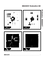
The MAX2057 evaluation boards can be used as a
guide for board layout. Pay close attention to thermal
design and placement of components on the PC board.
The exposed paddle (EP) on the MAX2057 package
conducts heat away from the die and provides a lowimpedance electrical connection. The EP must be
attached to the PC board ground plane with a low thermal and electrical impedance contact. Ideally, this is
provided by soldering the backside package contact
directly to a metal ground plane on the PC board.
Alternatively, the EP can be connected to a ground
plane using an array of plated vias directly below the
EP. The MAX2057 EV kit uses nine evenly spaced,
0.016in-diameter, plated through holes to connect the
EP to the lower ground planes.
Configuration B) To use only the attenuator between IC
pins 2 and 8: Move capacitor C3 to connect the pin 2
trace of the IC to the trace of connector J1. Apply the RF
input signal to SMA J4 and take the output signal from
SMA J1.
_______________________________________________________________________________________
3
Evaluates: MAX2057
VCNTL
The VCNTL pin is used to control the gain of the amplifier. The nominal operating range for the VCNTL pin is
from 1V to 4.5V. Limiting VCNTL to this range ensures
reliability of the device. Due to on-chip ESD diodes, do
not apply VCNTL without VCC (+5V) present. If this condition is unavoidable, then change R4 on the EV kit to a
resistor no smaller than 200Ω. This resistor will limit the
current into the VCNTL pin for cases where V CC is
grounded or left open.