1
DATA SHEET
ST10F167
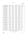
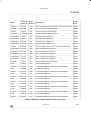
Input(I)/
Output(O)
Symbol
Pin
P3.0P3.13,
P3.15
65 – 70,
73 – 80,
81
I/O
I/O
I/O
65
66
67
68
69
70
I
O
I
O
I
I
73
74
I
I
75
76
77
78
79
80
81
I/O
I/O
O
I/O
O
O
I/O
O
85 - 92
I/O
85
90
O
O
I
O
O
O
P4.0 –
P4.7
91
92
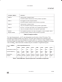
Function
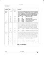
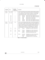
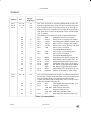
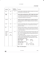
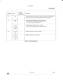
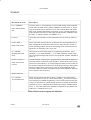
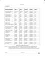
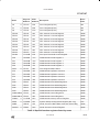
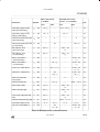
Port 3 is a 15-bit (P3.14 is missing) bidirectional I/O port. It is
bit-wise programmable for input or output via direction bits. For
a pin configured as input, the output driver is put into high-impedance state. Port 3 outputs can be configured as push/pull or
open drain drivers. The input threshold of Port 3 is selectable
(TTL or special).
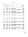
The following Port 3 pins also serve for alternate functions:
P3.0
T0IN
CAPCOM Timer T0 Count Input
P3.1
T6OUT
GPT2 Timer T6 Toggle Latch Output
P3.2
CAPIN
GPT2 Register CAPREL Capture Input
P3.3
T3OUT
GPT1 Timer T3 Toggle Latch Output
P3.4
T3EUD
GPT1 Timer T3 Ext.Up/Down Ctrl.Input
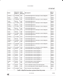
P3.5
T4IN
GPT1 Timer T4 Input for
Count/Gate/Reload/Capture
P3.6
T3IN
GPT1 Timer T3 Count/Gate Input
P3.7
T2IN
GPT1 Timer T2 Input for
Count/Gate/Reload/Capture
P3.8
MRST
SSC Master-Rec./Slave-Transmit I/O
P3.9
MTSR
SSC Master-Transmit/Slave-Rec. O/I
P3.10
TxD0
ASC0 Clock/Data Output (Asyn./Syn.)
P3.11
RxD0
ASC0 Data Input (Asyn.) or I/O (Syn.)
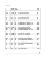
P3.12
BHE
Ext. Memory High Byte Enable Signal,
WRH
Ext. Memory High Byte Write Strobe
P3.13
SCLK
SSC Master Clock Outp./Slave Cl. Inp.
P3.15
CLKOUT System Clock Output (=CPU Clock)
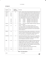
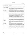
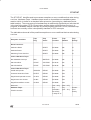
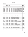
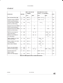
Port 4 is an 8-bit bidirectional I/O port. It is bit-wise programmable for input or output via direction bits. For a pin configured as
input, the output driver is put into high-impedance state.
In case of an external bus configuration, Port 4 can be used to
output the segment address lines:
P4.0
A16
Least Significant Segment Addr. Line
P4.5
A21
Segment Address Line,
CAN_RxD CAN Receive Data Input
P4.6
A22
Segment Address Line,
CAN_TxD CAN Transmit Data Output
P4.7
A23
Most Significant Segment Addr. Line
Table 1 Pin description
8/78
42-1701-03