1
UM10732
NXP Semiconductors
Chapter 4: LPC11U6x/E6x System configuration (SYSCON)
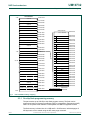
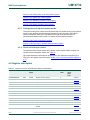
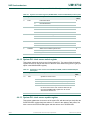
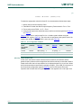
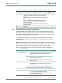
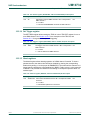
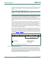
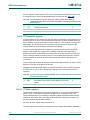
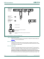
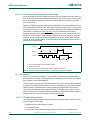
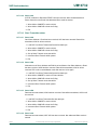
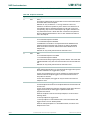
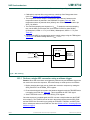
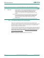
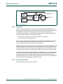
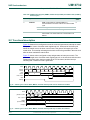
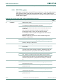
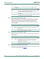
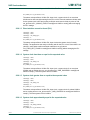
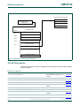
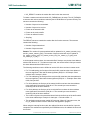
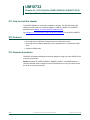
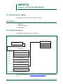
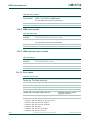
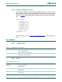
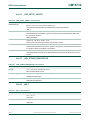
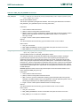
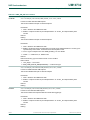
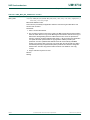
Section 4.4.46 “Deep-sleep mode configuration register”
Section 4.4.3 “System PLL control register”
Section 4.4.9 “Watchdog oscillator control register”
Section 4.4.8 “System oscillator control register”
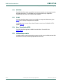
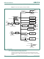
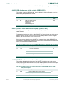
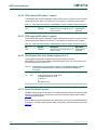
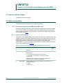
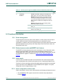
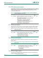
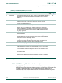
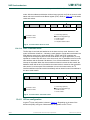
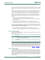
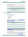
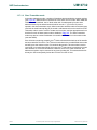
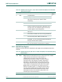
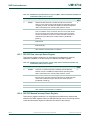
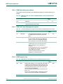
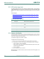
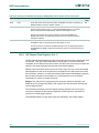
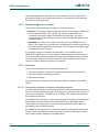
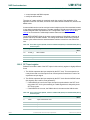
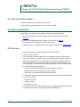
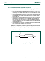
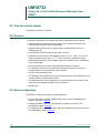
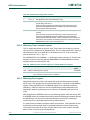
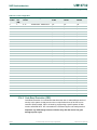
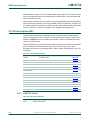
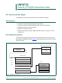
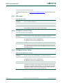
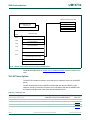
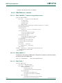
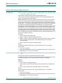
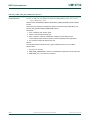
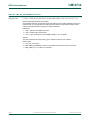
4.3.3 Configuration of reduced power-modes
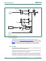
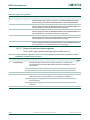
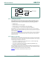
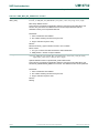
The system control block configures analog blocks that can remain running in the reduced
power modes (the BOD and the watchdog oscillator for safe operation) and enables
various interrupts to wake up the chip when the internal clocks are shut down in
Deep-sleep and Power-down modes. For details, see the following registers:
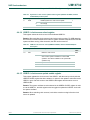
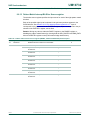
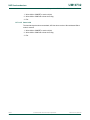
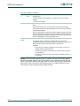
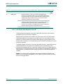
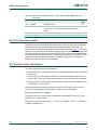
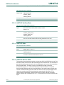
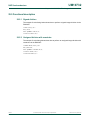
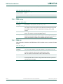
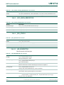
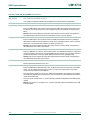
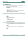
Section 4.4.48 “Power configuration register”
Section 4.4.45 “Start logic 1 interrupt wake-up enable register”
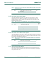
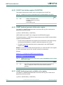
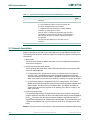
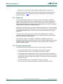
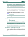
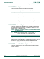
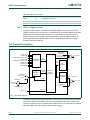
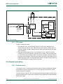
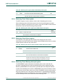
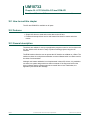
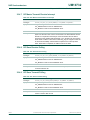
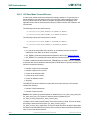
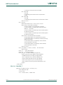
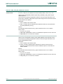
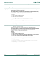
4.3.4 Reset and interrupt control
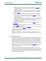
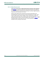
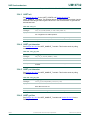
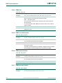
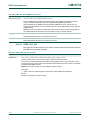
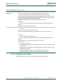
The peripheral reset control register in the system control register allows to assert and
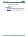
release individual peripheral resets. See Table 23.
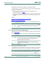
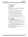
Up to eight external pin interrupts can be assigned to any digital pin except PIO2_8 to
PIO2_23 in the system control block (see Section 4.4.41 “Pin Interrupt Select registers 0
to 7”).
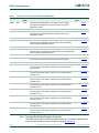
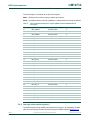
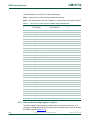
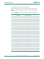
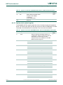
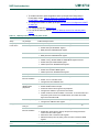
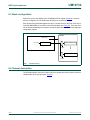
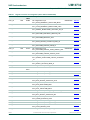
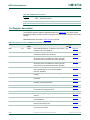
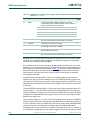
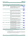
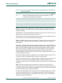
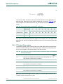
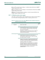
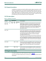
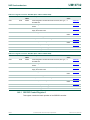
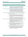
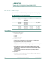
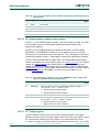
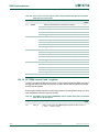
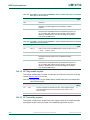
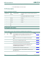
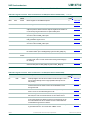
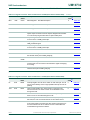
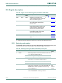
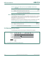
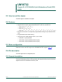
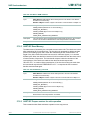
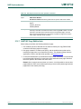
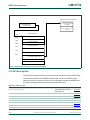
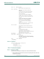
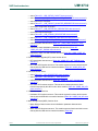
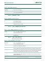
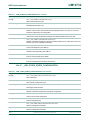
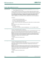
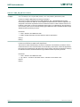
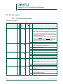
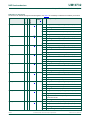
4.4 Register description
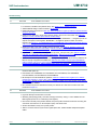
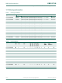
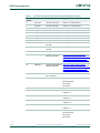
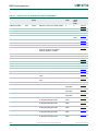
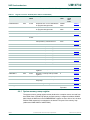
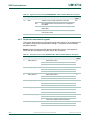
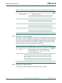
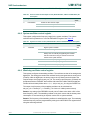
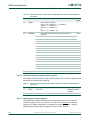
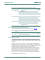
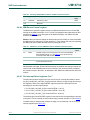
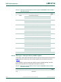
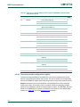
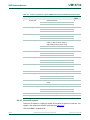
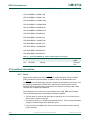
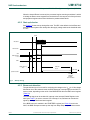
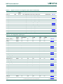
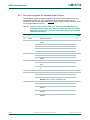
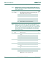
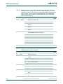
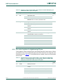
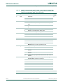
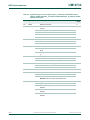
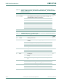
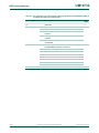
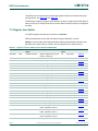
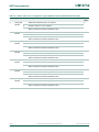
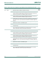
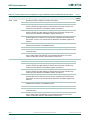
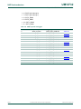
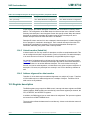
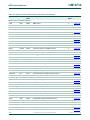
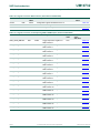
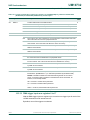
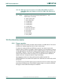
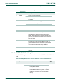
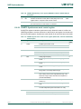
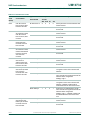
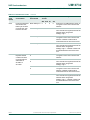
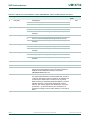
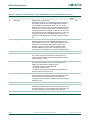
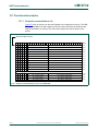
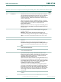
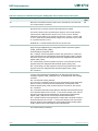
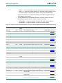
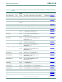
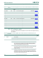
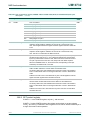
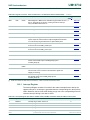
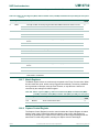
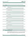
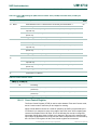
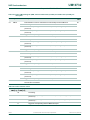
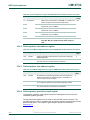
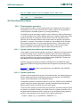
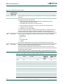
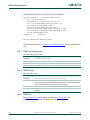
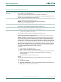
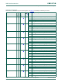
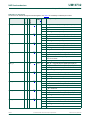
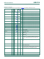
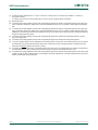
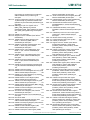
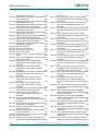
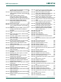
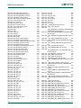
Table 21.
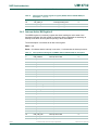
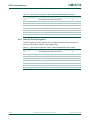
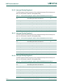
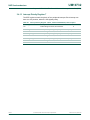
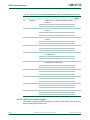
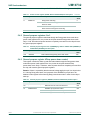
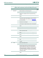
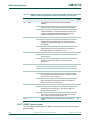
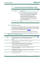
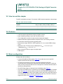
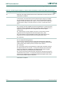
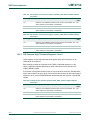
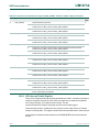
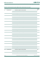
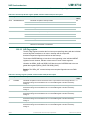
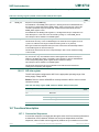
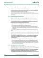
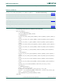
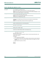
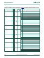
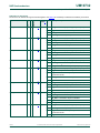
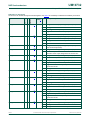
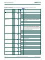
Register overview: SYSCON (base address: 0x4004 8000)
Name
Access
Address
offset
Description
Reset
value
Reset
value
after
boot
Reference
SYSMEMREMAP
R/W
0x000
System memory remap
0
Table 22
PRESETCTRL
R/W
0x004
Peripheral reset control
0
Table 23
SYSPLLCTRL
R/W
0x008
System PLL control
0
Table 24
SYSPLLSTAT
R
0x00C
System PLL status
0
Table 25
USBPLLCTRL
R/W
0x010
USB PLL control
0
Table 26
USBPLLSTAT
R
0x014
USB PLL status
0
Table 27
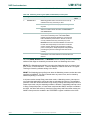
RTCOSCCTRL
R/W
0x01C
RTC oscillator 32 kHz output control
0x1
Table 28
SYSOSCCTRL
R/W
0x020
System oscillator control
0x000
WDTOSCCTRL
R/W
0x024
Watchdog oscillator control
0
0
Table 30
IRCCTRL
R/W
0x028
IRC control
0x080
-
Table 31
SYSRSTSTAT
R/W
0x030
System reset status register
0
Table 32
SYSPLLCLKSEL
R/W
0x040
System PLL clock source select
0
Table 33
SYSPLLCLKUEN
R/W
0x044
System PLL clock source update
enable
0x1
USBPLLCLKSEL
R/W
0x048
USB PLL clock source select
0
UM10732
User manual
All information provided in this document is subject to legal disclaimers.
Rev. 1.4 — 28 October 2015
Table 29
0x1
Table 34
Table 35
© NXP B.V. 2015. All rights reserved.
32 of 610