1
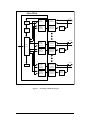
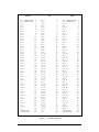
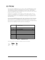
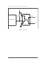
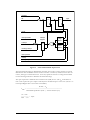
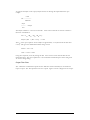
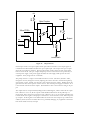
User Manual
IP-Unidig-I-O
-24I/O, -24I, -12I12O
24 Optically Isolated
Input/Output with Interrupts
IndustryPack®
Manual Revision: 2 8/2/99
Hardware Revision: A
IP-Unidig-I-O
-24I/O, -24I, -12I12O
24 Optically Isolated
Input/Output with Interrupts
IndustryPack®
This document contains information of proprietary interest to
GreenSpring Computers. It has been supplied in confidence
and the recipient, by accepting this material, agrees that the
subject matter will not be copied or reproduced, in whole or in
part, nor its contents revealed in any manner or to any person
except to meet the purpose for which it was delivered.
GreenSpring Computers has made every effort to ensure that
this manual is accurate and complete. Still, the company
reserves the right to make improvements or changes in the
product described in this document at any time and without
notice. Furthermore, GreenSpring Computers assumes no
liability arising out of the application or use of the device
described herein.
The electronic equipment described herein generates, uses, and
can radiate radio frequency energy. Operation of this
equipment in a residential area is likely to cause radio
interference, in which case the user, at his own expense, will be
required to take whatever measures may be required to correct
the interference.
GreenSpring’s products are not authorized for use as critical
components in life support devices or systems without the
express written approval of the president of GreenSpring
Computers, Inc.
This product has been designed to operate with IndustryPack
carriers and compatible user-provided equipment. Connection
of incompatible hardware is likely to cause serious damage.
GreenSpring Computers
1204 O'Brien Drive
Menlo Park, CA 94025
(415) 327-1200
(415) 327-3808 FAX
©1996 by GreenSpring Computers, Inc.
All rights reserved
IndustryPack is a registered trademark of GreenSpring Computers.
Macintosh is a registered trademark of Apple Computers.
Table of Contents
Product Description............................................................................................................................................... 1
VMEbus Addressing.............................................................................................................................................. 3
NuBus Addressing.................................................................................................................................................. 8
ISA (IBM PC-AT) Addressing............................................................................................................................. 9
I/O Pin Wiring ..................................................................................................................................................... 13
IndustryPack Logic Interface Pin Assignment............................................................................................... 15
Programming......................................................................................................................................................... 16
ID PROM .............................................................................................................................................................. 20
Theory of Operation............................................................................................................................................ 21
Construction and Reliability ............................................................................................................................... 29
Warranty and Repair ............................................................................................................................................ 30
Specifications......................................................................................................................................................... 31
Order Information ............................................................................................................................................... 32
Schematics.............................................................................................................................................................. 33
List of Figures
Figure 1
IP-Unidig-I-O Block Diagram.................................................................................................. 2
Figure 2
Word Access VME Address Map ............................................................................................ 3
Figure 3
Byte Access VME Address Map .............................................................................................. 5
Figure 4
Long Word Access VME Address Map.................................................................................. 7
Figure 5
Word Access ISA Address Map ............................................................................................... 9
Figure 6
Byte Access ISA Address Map................................................................................................ 11
Figure 7
I/O Pin Assignment ................................................................................................................. 14
Figure 8
Logic Interface Pin Assignment ............................................................................................. 15
Figure 9
Control Register Bit Definitions............................................................................................. 17
Figure 10
ID PROM Data (hex) ............................................................................................................... 20
Figure 11
Input Circuit ............................................................................................................................... 22
Figure 12
Internal Xilinx FPGA Input Circuit ...................................................................................... 23
Figure 13
Output Circuit............................................................................................................................ 25
Figure 14
I/O Circuit.................................................................................................................................. 27
Figure 15
Double Buffer ............................................................................................................................ 28
Product Description
The IP-Unidig-I-O is part of the IndustryPackTM family of modular I/O components. It provides
up to 24 lines of optically isolated digital I/O, with any input line capable of generating an interrupt.
It comes in three order options, the -12I12O has 12 dedicated inputs and 12 dedicated outputs, the 24I has 24 dedicated input lines, and the -24I/O has 24 lines which may be used as either input or
output. The -24I and -24I/O are Type III IP Modules with components mounted on the both sides
of the IP. The components on the back side have a maximum height of 0.140 inches.
The IP is built with optical couplers which have an isolation voltage of 2500 volts and a common
mode transient immunity of greater than 1000 volts/microsecond. Both transmitters and recievers
will operate at up to 1 Mbit/second.
The transmitters have an additional open collector transistor stage to increase the current drive
capabilities. Each transistor will sink up to 64 mA and has a 10K? pull up resistor standard.
Smaller pull up resistors may be substituted for faster turn on times as long as the current for the
Isolated VCC does not exceed 1A. A user provided external power supply of 5 to 20 volts powers
the user's equipment and the IP's isolated transmitters. The use of this power supply assures full
isolation between the user's system and the system containing the IP.
Writing a one to any output turns off the opto isolator, allowing the pull up resistor to set the line to
a passive logic high. Writing a zero to any output turns on the opto isolator, driving the line to a
logic low. All output lines may be enabled or disabled by writing a bit in the control register.
The isolated inputs have a series resistor which provides the current to turn on the opto-couplers
internal LED. The standard resistor is a 2K? , 8 pin, SIP resistor network, which gives an input
threshold of 2.5 V. When the voltage between the plus and minus inputs is greater than 2.5V, the
input will be read as a "1". It will be read as a "0" when the differential voltage is less than 2.5V.
Isolated input voltages are limited to 20 volts due to power dissipation in the resistor network. Users
may replace the 2K? SIP resistor networks with other values to change the threshold and maximum
voltages.
The interrupt latch circuits are edge sensitive with programmable polarity and are controlled through
the following five registers: Interrupt Pending, Interrupt Request, Interrupt Polarity, Interrupt
Enable, and Interrupt Clear. Each line corresponds to one bit in each of the registers, making
programming uniform and simple. This architecture also prevents the loss of an event during the
execution of the interrupt service routine.
With the -24IO order option, any line may be used as either input or output. If the data direction
will be dynamically changed, the minus side of the inputs must be tied to the isolated ground input.
The isolated inputs are limited to 20 V in this case. When the I/O line is used as an input, the
output must be left as a "1". This turns off the open collector output transistor allowing an external
source to drive the line.
The IP's double buffering capability makes it possible to update many outputs on several IPs
simultaneously. A user provided clock common to all the IP's is used to latch the ioutput registers.
The IP-Unidig-T is ideally suited to provide this clock, though any TTL compatible source may be
used. The input registers are always clocked by the IP Clock to ensure proper timing of the
interrupt circuits. Double buffering is controlled by a bit in the Control Register.
Reset disables all output transmitters and disables double buffering.
Figure 1 shows a block diagram of the IP-Unidig-I-O.
1
Xilinx FPGA
I/O 1+
Input 1
Opto Coupler
Input 1
Register
Clock
Control
Control
Register
I/P Bus
Interface
Output 1
Register
(-24I/O only)
Output 1
Opto Coupler
(-24I/O only)
Input 13
Register
(-24I and
-24IO only)
Input 13
Opto Coupler
(-24I and
-24IO only)
Output 13
Register
(-12I12O and
-24I/O only)
Output 13
Opto Coupler
(-12I12O and
-24I/O only)
Input 24
Register
(-24I and
-24IO only
Input 24
Opto Coupler
(-24I and
-24IO only)
Output 24
Register
(-12I12O and
-24IO only)
Output 24
Opto Coupler
(-12I12O and
-24IO only)
In 1—
Output
Transistor
Transistor
I/O 13+
In 13—
Output
Transistor
Transistor
I/O 24+
ID PROM
Figure 1
IP-Unidig-I-O Block Diagram
2
In 24—
Output
Transistor
Transistor
VMEbus Addressing
IP-Unidig-I-O normally is accessed one word at a time in the host's I/O space. Alternatively, byte
or long word accesses may be used. If long words are used, the host (or support module) must map
32-bit long words into two 16-bit cycles. This is common for 68020 and 68030 implementation of
the I/O space. The -12I12O option has Input lines 1— 12 and Output lines 13— 24. Only lines 1—
12 in all of the Interrupt Registers are valid for this option. The -24I does not have any Output
lines.
Standard Word Access, I/O Space
base + $0
base + $2
word
word
write
write
Output lines 1— 16
Output lines 17— 24
base + $0
base + $2
word
word
read
read
Read Back lines 1— 16
Read Back lines 17— 24
base + $4
base + $6
word
word
read
read
Direct Read lines 1— 16
Direct Read lines 17— 24
base + $C
word
read/write
Control Register
base + $10
word
read/write
Interrupt Vector Register
base + $12
base + $14
word
word
read/write
read/write
Interrupt Enable Register lines 1— 16
Interrupt Enable Register lines 17— 24
base + $16
base + $18
word
word
read/write
read/write
Interrupt Polarity Register lines 1— 16
Interrupt Polarity Register lines 17— 24
base + $1A
base + $1C
word
word
write
write
Interrupt Clear Register lines 1— 16
Interrupt Clear Register lines 17— 24
base + $1A
base + $1C
word
word
read
read
Interrupt Pending Register lines 1— 16
Interrupt Pending Register lines 17— 24
Figure 2
Word Access VME Address Map
Bit map of words at base + $0, base + $4, base + $12,
base + $16 and base + $1A
Data Bit #
I/O Line:
15
16
14
15
13
14
12
13
11
12
10
11
9
10
8
9
7
8
6
7
5
6
4
5
3
4
2
3
1
2
0
1
6
23
5
22
4
21
3
20
2
19
1
18
0
17
Bit map of words at base + $2, base + $6, base + $14,
base + $18 and base + $1C
Data Bit #
I/O Line:
15
-
14
-
13
-
12
-
11
-
10
-
9
-
3
8
-
7
24
Note: data in bits 15 through 8 are ignored in writes, read as "0"s.
Bit map of word at base + $C
Data Bit #
Write:
Read:
[15:3]
0
2
Mode Enable
Mode Enable
1
Clock Polarity
Clock Polarity
0
Dbl. Buffer En.
Dbl. Buffer En.
Bit map of the Interrupt Vector Register at base + $10
Data Bit #
Vec. Bit:
15
-
14
-
13
-
12
-
11
-
10
-
9
-
8
-
7
7
Note: data in bits 15 through 8 are ignored in writes, read as "0"s.
4
6
6
5
5
4
4
3
3
2
2
1
1
0
0
Alternate Byte Access, I/O Space
base + $0
base + $1
base + $3
byte
byte
byte
write
write
write
Output lines 9— 16
Output lines 1— 8
Output lines 17— 24
base + $0
base + $1
base + $3
byte
byte
byte
read
read
read
Read Back lines 9— 16
Read Back lines 1— 8
Read Back lines 17— 24
base + $4
base + $5
base + $7
byte
byte
byte
read
read
read
Direct Read lines 9— 16
Direct Read lines 1— 8
Direct Read lines 17— 24
base + $D
byte
read/write
Control Register
base + $11
byte
read/write
Interrupt Vector Register
base + $12
base + $13
base + $15
byte
byte
byte
read/write
read/write
read/write
Interrupt Enable Register lines 9— 16
Interrupt Enable Register lines 1— 8
Interrupt Enable Register lines 17— 24
base + $16
base + $17
base + $19
byte
byte
byte
read/write
read/write
read/write
Interrupt Polarity Register lines 9— 16
Interrupt Polarity Register lines 1— 8
Interrupt Polarity Register lines 17— 24
base + $1A
base + $1B
base + $1D
byte
byte
byte
write
write
write
Interrupt Clear Register lines 9— 16
Interrupt Clear Register lines 1— 8
Interrupt Clear Register lines 17— 24
base + $1A
base + $1B
base + $1D
byte
byte
byte
read
read
read
Interrupt Pending Register lines 9— 16
Interrupt Pending Register lines 1— 8
Interrupt Pending Register lines 17— 24
Figure 3
Byte Access VME Address Map
Bit map of bytes at base + $1, base + $5, base + $13,
base + $17 and base + $1B
Data Bit #
I/O Line:
7
8
6
7
5
6
4
5
3
4
2
3
1
2
0
1
Bit map of bytes at base + $0, base + $4, base + $12,
base + $16 and base + $1A
Data Bit #
I/O Line:
7
16
6
15
5
14
4
13
3
12
2
11
1
10
0
9
Bit map of bytes at base + $3, base + $7, base + $15,
base + $19 and base + $1D
Data Bit #
7
6
5
4
3
2
1
5
0
I/O Line:
24
23
22
21
20
19
18
17
Bit map of byte at base + $D
Data Bit #
Write:
Read:
[7:3]
0
2
Mode Enable
Mode Enable
1
Clock Polarity
Clock Polarity
Bit map of the Interrupt Vector Register at base + $11
Data Bit #
Vec. Bit:
7
7
6
6
5
5
4
4
3
3
2
2
1
1
6
0
0
0
Dbl. Buffer En.
Dbl. Buffer En.
Alternate Long Word Access, I/O Space
base + $0
long
write
Output lines 1— 24
base + $0
long
read
Read Back lines 1— 24
base + $4
long
read
Direct Read lines 1— 24
base + $C
long
read/write
Control Register
base + $10
long
read/write
Interrupt Vector Register
base + $12
long
read/write
Interrupt Enable Register lines 1— 24
base + $16
long
read/write
Interrupt Polarity Register lines 1— 24
base + $1A
long
write
Interrupt Clear Register lines 1— 24
base + $1A
long
read
Interrupt Pending Register lines 1— 24
Figure 4
Long Word Access VME Address Map
Bit map of long words at base + $0, base + $4, base + $12,
base + $16 and base + $1A
Data Bit #
I/O Line:
31
16
30
15
29
14
28
13
27
12
26
11
25
10
24
9
23
8
22
7
21
6
20
5
19
4
18
3
17
2
16
1
Data Bit #
I/O Line:
15
-
14
-
13
-
12
-
11
-
10
-
9
-
8
-
7
24
6
23
5
22
4
21
3
20
2
19
1
18
0
17
Note: data in bits 15 through 8 are ignored in writes, read as "0"s.
Bit map of long word at base + $C
Data Bit #
Write:
Read:
[31:19]
0
18
Mode Enable
Mode Enable
17
Clock Polarity
Clock Polarity
16
Dbl. Buffer En.
Dbl. Buffer En.
[15:0]
0
Note: data in bits 31 through 19 and 15 through 0 are ignored in writes, read as "0"s.
Bit map of long word at base + $10
Data Bit #
Vec. Bit:
31
-
30
-
29
-
28
-
27
-
26
-
25
-
24
-
23
7
22
6
21
5
20
4
19
3
18
2
17
1
16
0
Data Bit #
Vec. Bit:
15
-
14
-
13
-
12
-
11
-
10
-
9
-
8
-
7
-
6
-
5
-
4
-
3
-
2
-
1
-
0
-
Note: data in bits 15 through 8 are ignored in writes, read as "0"s.
7
NuBus Addressing
NuBus addressing requires computing the address from the byte addresses given above under
VMEbus Addressing. The formula is:
NuBus byte address = (VMEbus byte address * 2) – 1
All byte data is still transferred on data lines D7..D0.
Word addresses on the NuBus are the same as for VME. Word data is transferred on data lines
D15..D0.
8
ISA (IBM PC-AT) Addressing
IP-Unidig-I-O normally is accessed one word at a time in the host's I/O space. Alternatively, byte
accesses may be used. The actual application will depend on the carrier board. See the carrier board
manual for details. The -12I12O option has Input lines 1— 12 and Output lines 13— 24. Only lines
1— 12 in all of the Interrupt Registers are valid for this option. The -24I does not have any Output
lines.
Standard Word Access, I/O Space
base + $0
base + $2
word
word
write
write
Output lines 1— 16
Output lines 17— 24
base + $0
base + $2
word
word
read
read
Read Back lines 1— 16
Read Back lines 17— 24
base + $4
base + $6
word
word
read
read
Direct Read lines 1— 16
Direct Read lines 17— 24
base + $C
word
read/write
Control Register
base + $10
word
read/write
Interrupt Vector Register
base + $12
base + $14
word
word
read/write
read/write
Interrupt Enable Register lines 1— 16
Interrupt Enable Register lines 17— 24
base + $16
base + $18
word
word
read/write
read/write
Interrupt Polarity Register lines 1— 16
Interrupt Polarity Register lines 17— 24
base + $1A
base + $1C
word
word
write
write
Interrupt Clear Register lines 1— 16
Interrupt Clear Register lines 17— 24
base + $1A
base + $1C
word
word
read
read
Interrupt Pending Register lines 1— 16
Interrupt Pending Register lines 17— 24
Figure 5
Word Access ISA Address Map
Bit map of words at base + $0, base + $4, base + $12,
base + $16 and base + $1A
Data Bit #
I/O Line:
15
16
14
15
13
14
12
13
11
12
10
11
9
10
8
9
7
8
6
7
5
6
4
5
3
4
2
3
1
2
0
1
6
23
5
22
4
21
3
20
2
19
1
18
0
17
Bit map of words at base + $2, base + $6, base + $14,
base + $18 and base + $1C
Data Bit #
I/O Line:
15
-
14
-
13
-
12
-
11
-
10
-
9
-
8
-
7
24
Note: data in bits 15 through 8 are ignored in writes, read as "0"s.
9
Bit map of word at base + $C
Data Bit #
Write:
Read:
[15:3]
0
2
Mode Enable
Mode Enable
1
Clock Polarity
Clock Polarity
0
Dbl. Buffer En.
Dbl. Buffer En.
Bit map of the Interrupt Vector Register at base + $10
Data Bit #
Vec. Bit:
15
-
14
-
13
-
12
-
11
-
10
-
9
-
8
-
7
7
Note: data in bits 15 through 8 are ignored in writes, read as "0"s.
10
6
6
5
5
4
4
3
3
2
2
1
1
0
0
Alternative Byte Access, I/O Space
base + $0
base + $1
base + $2
byte
byte
byte
write
write
write
Output lines 1— 8
Output lines 9— 16
Output lines 17— 24
base + $0
base + $1
base + $2
byte
byte
byte
read
read
read
Read-back lines 1— 8
Read-back lines 9— 16
Read-back lines 17— 24
base + $4
base + $5
base + $6
byte
byte
byte
read
read
read
Direct Read lines 1— 8
Direct Read lines 9— 16
Direct Read lines 17— 24
base + $C
byte
read
Control Register
base + $10
byte
read/write
Interrupt Vector Register
base + $12
base + $13
base + $14
byte
byte
byte
read/write
read/write
read/write
Interrupt Enable Register lines 1— 8
Interrupt Enable Register lines 9— 16
Interrupt Enable Register lines 17— 24
base + $16
base + $17
base + $18
byte
byte
byte
read/write
read/write
read/write
Interrupt Polarity Register lines 1— 8
Interrupt Polarity Register lines 9— 16
Interrupt Polarity Register lines 17— 24
base + $1A
base + $1B
base + $1C
byte
byte
byte
write
write
write
Interrupt Clear Register lines 1— 8
Interrupt Clear Register lines 9— 16
Interrupt Clear Register lines 17— 24
base + $1A
base + $1B
base + $1C
byte
byte
byte
read
read
read
Interrupt Pending Register lines 1— 8
Interrupt Pending Register lines 9— 16
Interrupt Pending Register lines 17— 24
Figure 6
Byte Access ISA Address Map
Bit map of bytes at base + $0, base + $4, base + $12,
base + $16 and base + $1A
Data Bit #
I/O Line:
7
8
6
7
5
6
4
5
3
4
2
3
1
2
0
1
Bit map of bytes at base + $1, base + $5, base + $13,
base + $17 and base + $1B
Data Bit #
I/O Line:
7
16
6
15
5
14
4
13
3
12
2
11
1
10
0
9
Bit map of bytes at base + $2, base + $6, base + $14,
base + $18 and base + $1C
Data Bit #
7
6
5
4
3
2
1
11
0
I/O Line:
24
23
22
21
20
19
18
17
Bit map of byte at base + $C
Data Bit #
Write:
Read:
[7:3]
0
2
Mode Enable
Mode Enable
1
Clock Polarity
Clock Polarity
Bit map of the Interrupt Vector Register at base + $10
Data Bit #
Vec. Bit:
7
7
6
6
5
5
4
4
3
3
2
2
1
1
12
0
0
0
Dbl. Buffer En.
Dbl. Buffer En.
I/O Pin Wiring
This section gives the pin assignments and wiring recommendations for IP-Unidig-I-O.
The pin numbers given in Figure 7 below correspond to numbers on the 50-pin IndustryPack I/O
connector, to the wires on a 50-pin flat cable plugged into a standard IP carrier board, and to the
screw terminal numbers on the IP-Terminal block.
For the -24IO option, the inputs use two pins, the IO X+ and the In X– while the outputs only use
the IO X+ pin. The outputs are referenced to the Isolated GND, pin 50. Systems which will
dynamically switch lines between inputs and outputs must have the In X– pin tied to Isolated Gnd.
13
-12I12O
In 1+/Dbl Buf Clk+
In 1–/Dbl Buf Clk–
In 2+
In 2–
In 3+
In 3–
In 4+
In 4–
In 5+
In 5–
In 6+
In 6–
In 7+
In 7–
In 8+
In 8–
In 9+
In 9–
In 10+
In 10–
In 11+
In 11–
In 12+
In 12–
Out 13
n/c
Out 14
n/c
Out 15
n/c
Out 16
n/c
Out 17
n/c
Out 18
n/c
Out 19
n/c
Out 20
n/c
Out 21
n/c
Out 22
n/c
Out 23
n/c
Out 24
n/c
Isolated VCC
Isolated GND
-24I
1
2
3
4
5
6
7
8
9
10
11
12
13
14
15
16
17
18
19
20
21
22
23
24
25
26
27
28
29
30
31
32
33
34
35
36
37
38
39
40
41
42
43
44
45
46
47
48
49
50
In 1+
In 1–
In 2+
In 2–
In 3+
In 3–
In 4+
In 4–
In 5+
In 5–
In 6+
In 6–
In 7+
In 7–
In 8+
In 8–
In 9+
In 9–
In 10+
In 10–
In 11+
In 11–
In 12+
In 12–
In 13+
In 13–
In 14+
In 14–
In 15+
In 15–
In 16+
In 16–
In 17+
In 17–
In 18+
In 18–
In 19+
In 19–
In 20+
In 20–
In 21+
In 21–
In 22+
In 22–
In 23+
In 23–
In 24+
In 24–
n/c
n/c
Figure 7
-24IO
1
2
3
4
5
6
7
8
9
10
11
12
13
14
15
16
17
18
19
20
21
22
23
24
25
26
27
28
29
30
31
32
33
34
35
36
37
38
39
40
41
42
43
44
45
46
47
48
49
50
I/O Pin Assignment
14
I/O 1+/Dbl Buf Clk+ 1
In 1–/Dbl Buf Clk– 2
I/O 2+
3
In 2–
4
I/O 3+
5
In 3–
6
I/O 4+
7
In 4–
8
I/O 5+
9
In 5–
10
I/O 6+
11
In 6–
12
I/O 7+
13
In 7–
14
I/O 8+
15
In 8–
16
I/O 9+
17
In 9–
18
I/O 10+
19
In 10–
20
I/O 11+
21
In 11–
22
I/O 12+
23
In 12–
24
I/O 13+
25
In 13–
26
I/O 14+
27
In 14–
28
I/O 15+
29
In 15–
30
I/O 16+
31
In 16–
32
I/O 17+
33
In 17–
34
I/O 18+
35
In 18–
36
I/O 19+
37
In 19–
38
I/O 20+
39
In 20–
40
I/O 21+
41
In 21–
42
I/O 22+
43
In 22–
44
I/O 23+
45
In 23–
46
I/O 24+
47
In 24–
48
Isolated VCC
49
Isolated GND
50
15
IndustryPack Logic Interface Pin
Assignment
Figure 8 below gives the pin assignments for the IndustryPack Logic Interface on the
IP-Unidig-I-O. Pins marked n/c below are defined by the specification, but are not used on IPUnidig-I-O. Also see the User Manual for your IP Carrier board for more information.
GND
CLK
Reset*
D0 IDSel*
D1 n/c
D2 n/c
D3 n/c
D4 INTSel*
D5 n/c
D6 IOSel*
D7 n/c
D8 A1
D9 n/c
D10
D11
D12
D13
D14
D15
BS0*
BS1*
n/c
n/c
+5V
GND
GND
+5V
R/W*
4
5
6
7
8
9
10
11
12
13
A2
n/c
A3
IntReq0*
A4
n/c
A5
n/c
A6
Ack*
n/c
GND
1
26
2
3
27
28
29
30
31
32
33
34
35
36
37
38
14
15
16
17
18
19
20
21
22
23
39
40
41
42
43
44
45
46
47
48
24
25
49
50
Note 1: The no-connect (n/c) signals above are defined by the IndustryPack Logic Interface
Specification, but not used by this IP. See the Specification for more information.
Note 2: The layout of the pin numbers in this table corresponds to the physical placement of
pins on the IP connector. Thus this table may be used to easily locate the physical pin
corresponding to a desired signal. Pin 1 is marked with a square pad on the IndustryPack.
Figure 8
Logic Interface Pin Assignment
16
Programming
Programming the IP requires only the ability to read and write data in the host's I/O space. The
base address is determined by the IP Support Module. This document refers to this address as
"base".
After power on reset or VME system reset, the IP requires a minimum delay of 300 milliseconds
before any accesses are made by the host system. This is to allow the Xilinx FPGA to configured
itself. Any accesses during this time will result in a bus error. Reset disables the outputs and clears
all bits in the Control Register.
Inputs 1— 16 are read at address base + 4, inputs 17— 24 are read at address base + 6. The -12I12O
has inputs 1— 12 only. An input will be read as a "1" when the voltage between the plus and minus
input pins is greater than the threshold voltage. It will be read as a "0" when the voltage is less than
the threshold voltage. The IP comes standard with a 2K? series resistor which gives a threshold
voltage of 2.5V. See the Theory of Operation section for a description of how to determine the
threshold voltage.
Two order options, the -12I12O and -24IO have lines which may be used for outputs. The -12I12O
has 12 dedicated outputs while the -24IO has 24 lines which may be set on a per line basis for either
input or output. Both of these options have an enable bit, Bit[2] in the Control Register, which must
be set to a "1" before data written to the Output Register will appear on the outputs. When set to a
"0", all the output transistors will be turned off and the lines pulled up to a logic high. When set to a
"1", the output lines will follow the data written to the Output Register. Outputs 1— 16 are written
at address base + 0, outputs 17— 24 are written at address base + 2. The -12I12O option has
outputs 13— 24 only. To write a logic low on an output signal line, write a "0" to the Output bit
location. To write a logic high on an output signal line, write a "1" to the Output bit location.
For the -24IO option, any lines used as input must have their corresponding output lines set to a
"1". Writing a one and setting the signal line to input mode is the same. Passive pull-up resistors are
used with open collector drivers to implement the interface.
Using word access, up to 16 bits may be programmed at once. The IP implements a read back
register at the same address used for writing to the signal line Output bits. This permits "set bit" and
"clear bit" instructions to be used in programming, which are implemented by the host hardware as
read-modify-write cycles. Thus, single bits at well as bit fields may be accessed.
The IP may also be accessed using byte or long word accesses. If long word accesses are used from
a 68020, 68030, or 68040 host, the I/O space must be mapped into "D16". 68000 and 68010 hosts
internally map all long word accesses into 16 bits, so no special precaution is necessary.
The IP uses a Control Register to enable output double buffering and control the polarity of the
Double Buffer Clock. It also is used to enable the Output drivers. The -24I option does not
implement the Control Register because it does not have any outputs. Figure 9 below shows a table
of the Control Register.
17
Bit #
0
1
2
3— 7
Definition
Double Buffer Enable
Double Buffer Clock Polarity Select
Output Enable
Reserved
Figure 9
Access
Read/Write
Read/Write
Read/Write
Read as "0"
Control Register Bit Definitions
Control Register Bit Definitions:
Bit [0]
Double Buffer Enable (not applicable in the -24I option)
This bit enables double buffering. If this bit is set to a "1", the user must provide a clock on either
the Double Buffer Clock, pin 49, or the Slave Clock, pin 45, depending on how bit[3] is set. This
clock may be up to 1 MHz. Writing a "0" disables double buffering. This is the power up and reset
default.
Bit [1]
Double Buffer Clock Polarity Select (not applicable in the -24I option)
This bit controls the Double Buffer Clock polarity. Writing a "1" will cause output data to be
latched out of the IP on the falling edge of the Double Buffer Clock. Writing a "0" will cause data
to be latched on the rising edge of the Double Buffer Clock. This is the power up and reset default.
Bit [2]
Output Enable (not applicable in the -24I option)
This bit enables and disables the output drivers. Writing a "1" will enable the data written to the
Output Register to appear on the output lines. Writing a "0" will turn off all the output drivers,
setting all the output lines to a passive logic high through the pull-up resistors. This is the power up
and reset default. The -24I option will ignore this bit on writes and read it as a "0".
Bit [3— 7]
Reserved
These bits will be ignored during writes and read as "0"s. It is recommended they be written as "0"s.
Interrupts
The IP-Unidig-I-O uses five 24-bit registers (12 bits in the -12I12O option) to control interrupt
generation. Each bit in each register corresponds to one Input line, simplifying software
development. Inputs are not debounced. Users may need to provide this feature either in software
or with external hardware if noisy inputs, such as mechanical switches, are used to generate
interrupts. Interrupts from all Input lines are OR'd together and are asserted on IntReq0*. The IP
responds to an interrupt cycle be putting out its 8-bit vector from the Interrupt Vector Register onto
the data bus.
Interrupt Enable Register
The Interrupt Enable Register is used to enable and disable interrupts from individual Input lines.
Programming any bit to a "1" enables an interrupt from the corresponding Input line. Programming
any bit to a "0" disables an interrupt from the corresponding Input line.
For the IP to actually request an interrupt, an edge or level must be seen on the corresponding Input
line. Since the IP monitors interrupts regardless of the state of the enable bit, it is possible to get an
interrupt immediately upon enabling any bit in this register.
The Interrupt Enable Register is cleared on reset. Thus, all channels are disabled from generating
interrupts on reset.
18
Interrupt Polarity Register
The Interrupt Polarity Register is used to set the polarity of the transition which is to generate an
interrupt for each Input line. Programming any bit to a "1" will generate an interrupt when the input
data changes from a logic zero to a logic one on the corresponding Input line. Programming any bit
to a "0" will generate an interrupt when the input data changes from a logic one to a logic zero. For
the IP to actually request an interrupt, the corresponding bit in the Interrupt Enable Register must
be "1".
The Interrupt Polarity Register is cleared on reset. This makes the default to interrupt on a falling
edge for all Input lines.
The IP's logic monitors writing to this register. If a bit in this register is changed, and the static input
on the corresponding line matches the programmed bit, the interrupt flip-flop for that line is set.
This feature is critical to prevent the loss of an interrupt due to a line transition which might occur
during an interrupt service routine.
Example: The software reads an input, determines it is zero, then enables that line to generate an
interrupt on a rising edge. Between the read and the write, however, the input changed
to one. With this special logic, an interrupt is immediately generated, or generated at the
end of the current routine if interrupts are masked. Without the logic, the input
transition would have been lost.
If the software does not care what the current state of the Input lines are and does not wish to
receive any immediate interrupts, then the procedure is (1) disable interrupts in the processor, (2)
program the IP's Polarity Register, (3) write to all lines of the Clear Interrupt Register, (4) enable
interrupts in the processor.
Inverting a bit in this register each time the corresponding bit generates an interrupt will result in an
interrupt for both rising and falling edges.
Clear Interrupt Register and
Pending Interrupt Register
These two registers are used to detect and clear pending interrupts from any combination of lines.
Both registers access the same interrupt flip-flops. They are arranged as one read-only register, the
Pending Interrupt Register, and one write-only register, the Clear Interrupt Register.
The flip-flops that make up these two registers are set only by a transition on an Input line of the
programmed polarity. They are cleared by the software writing to the Clear Interrupt Register or by
IP Reset.
Reading a one in the Pending Interrupt Register means the corresponding Input line either has
generated an interrupt if that line is enabled, or has an interrupt pending if it is disabled. A pending
interrupt will drive the interrupt request line as soon as the corresponding bit in the Interrupt Enable
Register is set to "1".
Both interrupts and pending interrupts are cleared for any line by writing a one to the corresponding
bit position in the Clear Interrupt Register. In general, only Input lines which have been detected as
pending by a read of the Pending Interrupt Register should be cleared. This will prevent the loss of
an interrupt which arrives between the read and write. If the write to the Clear Interrupt Register
were to be all "1"s, an interrupt arriving on a new channel between the read and write would be lost.
Writing a "0" to any bit in the Clear Interrupt Register has no affect on the corresponding line.
Note that for simplicity, the host software need only read the Pending Interrupt Register, then
immediately write the same value to the Clear Interrupt Register. The software may then check the
19
bits in that byte, taking whatever actions are required by the one or more Input lines recognized to
need service.
To clear all pending and latent interrupts, the software writes all "1"s to the Clear Interrupt Register.
The Pending Interrupt register is cleared on reset, which clears all interrupts and pending interrupts.
Interrupt Vector Register
The IP has an eight bit read/write register to hold the interrupt vector required to service IP
interrupts.
All interrupts from one IP-Unidig-I-O use the same vector. The Pending Interrupt Register is used
to determine what combination of channels need service. This allows the software to handle any
number of equally weighted channels in a single interrupt service routine.
This register is cleared on reset.
Double Buffering
Double buffering is a feature which allows all the outputs to be latched at the same time, whether on
a single IP or a system with multiple IPs. This is useful for systems which require many outputs to
be updated simultaneously. Inputs are not double buffered to ensure proper timing for the interrupt
circuits. To use double buffering, an external clock must be provided on Pins 1 and 2, the Double
Buffer Clock+ and Double Buffer Clock– pins. Double buffering is turned on by setting the
Double Buffer Enable bit, Bit [0], in the Control Register to a "1". The Double Buffer Clock
polarity is programmable via the Double Buffer Clock Polarity bit, Bit [1], in the Control Register.
Setting this bit to a "0" will cause the outputs to be latched on the rising edge of the Double Buffer
Clock, while setting the bit to "1" will latch the outputs on the falling edge. Double buffering is not
available on the -24I because it has no outputs.
20
ID PROM
Every IP contains an IP PROM, whose size is at least 12 x 8 bits. The ID PROM aids in software
auto configuration and configuration management. The user’s software, or a supplied driver, may
verify that the device it expects is actually installed at the location it expects and is nominally
functional. The ID PROM contains the manufacturing revision level of the IP. If a driver requires a
particular revision IP, it may check for it directly.
Standard data in the ID PROM on the IP-Unidig-I-O is shown in Figure 10 below. For more
information on IP ID PROMs refer to the IndustryPack Logic Interface Specification, available
from GreenSpring Computers, Inc.. The ID PROM on the IP-Unidig-I-O is implemented in the
Xilinx FPGA device.
The location of the ID PROM in the host’s address space is dependent on the carrier board used.
For most VMEbus carriers the ID PROM space is directly above the IP’s I/O space, or at IP-base +
$80. Macintosh drivers use the ID PROM automatically. RM1260 address may be derived from
Figure 10 below by multiplying the addresses given by two, then subtracting one. RM1270 addresses
may be derived by multiplying the addresses given by two, then adding one.
1F
19
17
15
13
11
0F
0D
0B
09
07
05
03
01
(available for user)
CRC for bytes used
No of bytes used
Driver ID, high byte
Driver ID, low byte
reserved
Revision
Model No
Manufacturer ID GreenSpring
ASCII “C”
ASCII “A”
ASCII “P”
ASCII “I”
Figure 10
see table below
(0C)
(00)
(00)
(00)
(A1)
see table below
(F0)
(43)
(41)
(50)
(49)
ID PROM Data (hex)
The following table lists the Model No. and CRC for the three order options.
-24IO
-12I12O
-24I
Model No.
0x6A
0x70
0x66
CRC
0x8D
0xB8
0xE6
21
Theory of Operation
IndustryPack Standards
The IP-Unidig-I-O is part of the IndustryPackTM family of modular I/O products. It meets the
IndustryPack Logic Specification. (Contact GreenSpring Computers, Inc. for a copy of this
Specification.) It is assumed the reader is at least casually familiar with both this document and
68000 processor architecture.
Control Logic
All control logic is contained within a single Xilinx FPGA. It is clocked by the 8 MHz IP Logic
clock from the Support Module. The IP responds to I/O and ID selects. It does not respond to
memory selects, however the MEMSel* line is routed to the FPGA, enabling easy modification for
special needs.
The IP does not require wait states for either read or write cycles. Thus, the FPGA generates Ack*
on the clock cycle following either I/O or ID Select. Hold cycles (from the Support Module) are
supported for both read and write cycles by extending Ack* as required. If no hold cycles are
requested by the Support Module, the IP is capable of supporting the full 8 MByte per second data
transfer rate of the IP Logic Interface Specification.
Input Data Lines
The -24I option has 24 dedicated inputs, the -12I12O has 12 dedicated inputs and the -24IO has 24
lines which may be used either for input or output. Each input uses a Siemens SHF6313 Opto
Coupler to provide the optical isolation. They have an LED on the input side and a photo detector
connected to the base of a transistor on the output. The collector of the coupler's output transistor
is connected to the input on the Xilinx FPGA and a 47K? pull-up resistor. The FPGA inverts the
input to make it positive true logic.
Interrupts
The interrupt generation circuitry consists of an edge detector and a level sensor which feed the
input of a latch. The edge detector uses two latches in series clocked by the 8 MHz IP Clock to
compare the current state of the Input line with the previous state. If the two states are different
and the difference matches the polarity set in the Polarity Register, the Interrupt Latch is set. If the
Interrupt Enable bit is set for that I/O line, an interrupt is generated on IntReq0*. This series of
latches means there will be a minimum 125 ns. delay (one 8 MHz clock pulse) from the time the
I/O line transitions until the interrupt is generated. Individual interrupts are cleared by writing a "1"
to the corresponding bit in the Interrupt Clear Register.
The level sensor is only active when writing to the Interrupt Polarity Register. If a "1" is written to a
bit in the Interrupt Polarity Register, corresponding to a rising edge interrupt, and the level on the
Input line is already a "1", the level sensor will generate a pending interrupt. If the Interrupt Enable
bit is set for that Input line, an interrupt is generated on IntReq0*. This can be used to ensure an
edge will not be missed when generating interrupts on both the rising and falling edge. In this case,
the interrupt service routine (ISR) should change the Interrupt Polarity Register. If the Input line
has transitioned already, an interrupt will be generated immediately. When the ISR completes, the
interrupt will be waiting.
If a bit is used as an output, it will still generate an interrupt when it is written to if the
corresponding bit in the Interrupt Enable Register is set. If this is undesired, care must be taken to
enable interrupts only for those bits used as input.
22
Figures 11 and 12 show diagrams of the structure for each Input line.
+5V
47Kž
Opto Coupler
2Kž
In+
Xilinx FPGA
In–
Figure 11
Input Circuit
23
Read En
Dx
Q D
Q D
Input
IP Clk
Interrupt Enable
Interrupt
Interrupt
Register
Edge
Detect
Q D
Level
Detect
Pending Interrupt
Interrupt Clear
Polarity
Polarity Chip Select Pulse
Figure 12
Internal Xilinx FPGA Input Circuit
The input threshold voltage is determined by the input series resistor. These resistors are in 8 pin
SIP networks with 4 individual resistors and are in sockets. The factory standard value is 2K? 5%
resistor, which gives a threshold of 2.5V. Users may replace the resistors to change the threshold.
Use the following formulas to determine the threshold voltage.
The opto coupler has a minimum current transfer ratio (CTR) of 19%. The Vil of the FPGA is
0.8V. This requires the opto coupler to sink 94µA for the FPGA input to sense a low (read as a "1"
in the Input Register due to an inverter in the FPGA).
IP VCC – Vil
I sink = — — — — — — — — — — — — — — — — — — — — — — — —
Internal Pull-up Resistor (47K? ) – resistor tolerance (5%)
5V – 0.8V
— — — — — = 94µA
47K? – 5%
24
To generate the 94µA on the output, 495µA must be run through the input LED of the opto
coupler.
I sink
I in = — — — —
CTR min.
94µA
———
19%
= 495µA
The 495µA translates to 1.04 V across the 2K? series resistor when the 5% resistor tolerance is
taken into consideration.
Vres = I in x (Rin + (Rin x Rin tol.))
495µA x (2K? + (2K? x 5%)) = 1.04V
The VF of the opto coupler at an IF of 495µA is approximately 1.4 V (taken from the data sheet
curves). This gives the minimum threshold voltage of 2.5V
Vthesh = Vres + VF
1.04V + 1.45V = 2.49V
Using these equations, users may change the 2K? series resistors values and calculate the new
threshold voltage. The opto couplers have a 25 mA absolute maximum input current rating and a
3V reverse voltage rating.
Output Data Lines
The -12I12O has 12 dedicated outputs and the -24IO has 24 lines which may be used either for
input or output. The -24I option does not have outputs. Figure 13 shows a diagram of one output.
25
560ž
+5V
Isolated VCC
Opto Coupler
10Kž
Xilinx FPGA
Output Enable
Dx
Output
D Q
3.9Kž
Latch Clk
Isolated GND
Figure 13
Output Circuit
Each output consists of an opto coupler and an open collector transistor. The output register is
contained in the Xilinx FPGA and drive the opto coupler input. The output of the opto coupler
drives the open collector transistor. This provides 64 mA of sink current for each output with a
limit of 1A for the IP. The opto coupler and pull-up resistor on the transistor are powered by an
external power supply. This power supply should be the same supply which powers the user's
equipment. It may range from 5V to 20V DC.
The pull-up resistor is a 9 pin, 8 resistor SIP network in a socket. The factory default is 10K? ,
though the user may change this value by replacing the resistor networks. Each network pulls up
eight outputs. In the -12I12O, one network is only connected to four outputs. Smaller values will
give faster rise times at the expense of drive current. The external power supply is limited to 1A as
is the total sink current for all the outputs. This limitation is due to the connector rating of 1A per
pin.
The outputs have an output enable bit, Bit[2] in the Control Register, which controls all the output
lines. When it is set to "0", all the outputs will be disabled and the lines will be pulled up to a
passive high. This is the power up and reset state. When it is set to "1", the outputs will follow the
contents of the write register. The purpose of this bit is to ensure the lines on the -24IO will power
up as inputs. All the registers in the Xilinx FPGA are cleared on reset and power up. Without the
enable bit, all the I/O lines would be driven low, potentially damaging any equipment connected to
lines which will be used only for input.
26
-24IO Option
The lines on the -24IO Option may be used for either input or output. This requires some special
considerations because the input and output circuits are connected. Figure 14 shows a schematic
diagram. By connecting the minus side of the input to isolated ground, both the inputs and outputs
will track. That is, the input will read a one when the output is set to one and read a zero when the
output is set to zero. The combination of the output pull-up resistor and input series resistor must
be small enough to generate the 495µA current to turn on the input opto coupler. Without this, the
input will not read a one when the output is set to one. If reads and writes don't need to track the
minus side does not have to be connected to isolated ground. However, the minus side must not be
more than 3V higher than isolated ground when the output transistor is turned on, driving the I/O
line low.
27
560ž
+5V
Isolated VCC
Opto Coupler
10Kž
Xilinx FPGA
3.9Kž
I/O +
+5V
47Kž
Opto Coupler
2Kž
Isolated GND
In–
Figure 14
I/O Circuit
28
Double Buffering
Each output has two latches associated with it. If double buffering is enabled, the Double Buffer
Latch is clocked by the Double Buffer Clock. The Double Buffer Clock may be up to 500 KHz.
Without double buffering, the latches are clocked on the rising edge of the IP Clock. Figure 15
shows a schematic diagram. Outputs from the Double Buffer Latch directly drive the minus side of
the output opto couplers. Data is latched into the internal latch on the rising edge of the IP Clock
after the Ack* line is driven low. Double Buffering is not available for the Input lines to ensure
proper timing of the interrupt circuitry.
Readback En
Dx
Internal Latch
Write En
IP Clk
Double Buffer Latch
D Q
D Q
CE
Out x
Latch Clk
In 1
Double Buf. Pol.
Double Buf. En.
Figure 15
Double Buffer
Double buffering is enabled by setting the Double Buffer Enable Bit (bit [0]) in the Control Register
to a "1". If double buffering is enabled, the Double Buffer Clock Polarity Bit (bit [1]) in the
Control Register is used to set the Double Buffer Clock polarity. Setting the Double Buffer Clock
Polarity Bit to a "0" will latch data on the rising edge and setting it to a "1" will latch data on the
falling edge. The power up default is "0" for both these bits.
29
Construction and Reliability
IndustryPacks were conceived and engineered for rugged industrial environments. The IP-UniDig-D
is constructed out of 0.062 inch thick FR4 V0 material. The six copper layers consist of two signal
layers on the top and bottom, and four internal layers. Two internal layers are dedicated to power
and ground planes and two are used for signal wiring.
Through hole and surface mounting of components are used. IC sockets use gold plated screwmachine pins. High insertion and removal forces are required, which assists in keeping components
in place. If the application requires unusually high reliability or is in an environment subject to high
vibration, the user may solder the four corner pins of each socketed IC into the socket, using a
grounded soldering iron.
The IndustryPack connectors are keyed, shrouded and have gold plated pins on both plugs and
receptacles. They are rated at 1 Amp per pin, 200 insertion cycles minimum. These connectors make
consistent, correct insertion easy and reliable.
The IP is secured to the carrier with four M2 metric stainless steel screws. The heads of the screws
are countersunk into the IP. The four screws provide significant protection against shock, vibration
and incomplete insertion. For most applications they are not required.
The IndustryPack provides a low temperature coefficient of 0.89 W/°C for uniform heat. This is
based on the temperature coefficient of the base FR4 material of 0.31 W/m-°C, taking into account
the thickness and area of the IP. This coefficient means that if 0.89 Watts is applied uniformly on
the component side, then the temperature difference between the component and the solder side is
one degree Celsius.
30
Warranty and Repair
GreenSpring Computer warrants this product to be free from defects in workmanship and materials
under normal use and service and in its original, unmodified condition, for a period of one year from
the time of purchase. If the product is found to be defective within the terms of this warranty,
GreenSpring Computer’s sole responsibility shall be to repair, or at GreenSpring Computer’s sole
option to replace, the defective product. The product must be returned by the original customer,
insured, and shipped prepaid to GreenSpring Computers. All replaced products become the sole
property of GreenSpring Computers.
GreenSpring Computer’s warranty of and liability for defective products is limited to that set forth
herein. GreenSpring Computers disclaims and excludes all other product warranties and product
liability, expressed or implied, including but not limited to any implied warranties of
merchandisability or fitness for a particular purpose or use, liability for negligence in manufacture or
shipment of product, liability for injury to persons or property, or for any incidental or consequential
damages.
GreenSpring’s products are not authorized for use as critical components in life support devices or
systems without the express written approval of the president of GreenSpring Computers, Inc.
Service Policy
Before returning a product for repair, verify as well as possible that the suspected unit is at fault.
Then call the Customer Service Department for a RETURN MATERIAL AUTHORIZATION
(RMA) number. Carefully package the unit, in the original shipping carton if this is available, and
ship prepaid and insured with the RMA number clearly written on the outside of the package.
Include a return address and the telephone number of a technical contact. For out-of-warranty
repairs, a purchase order for repair charges must accompany the return. GreenSpring Computers will
not be responsible for damages due to improper packaging of returned items. For service on
GreenSpring Products not purchased directly from GreenSpring Computers contact your reseller.
Products returned to GreenSpring Computers for repair by other than the original customer will be
treated as out-of-warranty.
Out of Warranty Repairs
Out of warranty repairs will be billed on a material and labor basis. The current minimum repair
charge is $100. Customer approval will be obtained before repairing any item if the repair charges
will exceed one half of the quantity one list price for that unit. Return transportation and insurance
will be billed as part of the repair and is in addition to the minimum charge.
For Service Contact:
Customer Service Department
GreenSpring Computers
1204 O’Brien Drive
Menlo Park, CA 94025
(415) 327-1200
(415) 327-3808 fax
31
Specifications
Digital Interface
IP-Unidig-O–12I12O:
IP-Unidig-O–24IO:
IP-Unidig-O–24I:
12 dedicated optically isolated latched
inputs, 12 dedicated optically
isolated double buffered outputs
24 optically isolated double buffered
I/O lines
24 dedicated optically isolated latched
inputs
Output Interface Level
0 volts to External Power Supply, 20 volts max., 64 mA
10 K? pullup resistor standard
Input Interface Level
Standard: 0 V to 20 V Common Mode, 500 µA min.
Output Update Rate
1 Mbit/second maximum
Isolation Voltage
100 volts min. This voltage is also dependent on the carrier board
isolation and may be less for some carrier boards.
Software Interface
Seven 24-bit registers:
Output
Read Back
Input
Interrupt Enable
Interrupt Pending
Interrupt Polarity
Interrupt Clear
Two 8-bit registers:
Control
Interrupt Vector
Initialization
300 Millisecond delay from reset
Forces all lines to be inputs
Disables double buffering
Access Mode
Byte or word in I/O Space
Wait States
Zero
Transfer Rate
8 Mbytes/second maximum, continuous
Onboard Options
All options are software programmable
Dimensions
Standard Single High IndustryPack width and length
1.8 x 3.9 inches
IP-Unidig-O–12I12O: Type I
IP-Unidig-O–24IO:
Type III, max. height: 0.14"
IP-Unidig-O–24I:
Type III, max. height: 0.14"
Construction
Conformal Coated FR4 4 layer Printed Circuit
Surface mounted components
Temperature
Coefficient
0.89 W/°C for uniform heat across IP
32
Power Requirements
+5.0 VDC, 510 mA typical
33