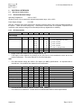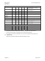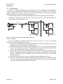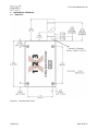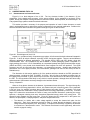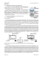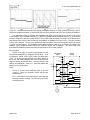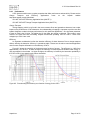
1
X-123 User Manual Rev A0 X-123 Complete X-Ray Spectrometer with CdTe Detector User Guide and Operating Instructions Amptek, Inc. 14 DeAngelo Dr. Bedford, MA 01730 PH: +1 781-275-2242 FAX: +1 781-275-3470 [email protected] www.amptek.com Amptek Inc. Page 1 of 42 X-123 User Manual Rev A0 Table of Contents 1 1.1 Introduction........................................................................................................................................3 Description ....................................................................................................................................3 2 Specifications ....................................................................................................................................4 3 Cautions and Warnings .....................................................................................................................7 4 Getting Started ..................................................................................................................................8 4.1 Equipment List ..............................................................................................................................8 4.2 Notes.............................................................................................................................................8 4.3 Making connections ......................................................................................................................8 4.4 Install Software..............................................................................................................................9 4.5 Configuring the unit.....................................................................................................................10 4.5.1 Regions of Interest (ROI) ...................................................................................................11 4.5.2 Calibrating the Horizontal Axis ...........................................................................................11 4.6 Troubleshooting ..........................................................................................................................12 5 Electrical Interfaces .........................................................................................................................13 5.1 Electrical specifications...............................................................................................................13 5.1.1 Absolute Maximum Ratings ...............................................................................................13 5.1.2 DC Characteristic ...............................................................................................................13 5.2 Communication ...........................................................................................................................14 5.3 Auxiliary Input and Outputs.........................................................................................................15 5.4 Timing of Auxiliary Inputs and Outputs .......................................................................................16 5.5 Power Interface ...........................................................................................................................18 6 6.1 6.2 6.3 Mechanical Interface .......................................................................................................................20 Dimensions .................................................................................................................................20 Mounting Hardware.....................................................................................................................21 Connectors..................................................................................................................................21 7.1 7.2 7.3 7.4 Software Interface ...........................................................................................................................23 Interface Software .......................................................................................................................23 Embedded Software ...................................................................................................................23 Boot Flags ...................................................................................................................................23 Upload Manager..........................................................................................................................25 7 8 Understanding the X-123 ................................................................................................................27 8.1 Understanding the Complete System .........................................................................................27 8.2 Understanding the Detector and Preamplifier.............................................................................29 8.2.1 Design and Operation ........................................................................................................29 8.2.2 Performance.......................................................................................................................31 8.3 Understanding the Digital Processor ..........................................................................................32 8.3.1 Major Function Blocks ........................................................................................................32 8.3.2 Analog Prefilter...................................................................................................................33 8.3.3 Pulse Shaping ....................................................................................................................35 8.3.4 Pulse Selection...................................................................................................................36 8.3.5 MCA, MCS, Counters, and SCAs ......................................................................................38 8.3.6 Electrical & Software Interfaces .........................................................................................40 8.4 Understanding the Power Supplies.............................................................................................41 9 9.1 Application notes .............................................................................................................................42 Do’s and Don’ts...........................................................................................................................42 Amptek Inc. Page 2 of 42 X-123 User Manual Rev A0 1 INTRODUCTION 1.1 DESCRIPTION The X-123 combines in a single package Amptek’s high performance X-ray spectroscopy components: (1) the XR-100T-CdTe X-ray and gamma-ray detector and preamplifier, (2) the DP5 digital pulse processor and MCA, and (3) the PC5 power supply. The result is a complete system which can fit in your hand with no performance compromise. It requires only +5 VDC power and a standard communication interface. With the X-123 anyone can rapidly obtain high quality X-ray spectra. The X-123 uses a CdTe crystal as x-ray and gamma-ray detector. The CdTe is mounted on a thermoelectric cooler along with the input FET and coupled to a custom charge sensitive preamplifier. The thermoelectric cooler reduces the electronic noise in the detector and preamplifier but the cooling is transparent to the user: it operates like a room temperature system. The pulse processor is the DP5, a second generation digital pulse processor (DPP) which replaces both the shaping amplifier and MCA found in analog systems. The digital technology improves several key parameters: (1) better performance, specifically better resolution and higher count rates; (2) greater flexibility since more configuration options are available and selected by software, and (3) improved stability and reproducibility. The DPP digitizes the preamplifier output, applies real-time digital processing to the signal, detects the peak amplitude, and bins this in its histogram memory. The spectrum is then transmitted to the user’s computer. The PC5 supplies the power to the detector, including low voltages for the preamps, high voltage to bias the detector, and a supply for the thermoelectric cooler which provides closed loop control with a maximum temperature differential of 85 °C. All of these are under software control. The X-123 input power is unregulated +5 VDC with a current of about 500 mA. The complete system is packaged in 7 x 10 x 2.5 cm3 aluminum box. The detector is mounted on an extender, with lengths from 0 to 9” (vacuum flanges are available). In its standard configuration only two connections are required: power (+5 VDC) and communications (USB, RS232, or Ethernet). An auxiliary connector provides several additional inputs and outputs used if the X-123 will be integrated with other equipment. This includes an MCA gate, timing outputs, and eight SCA outputs. The X-123 is supplied with data acquisition and control software. It also includes an Application Programming Interface (API) DLL to integrate the unit with custom software. Optional accessories include software for analyzing X-ray spectra, several collimation and mounting options, and X-ray tubes to complete a compact system for X-ray fluorescence. Figure 1-1. Photograph of complete X-123 (left) and a typical 57Co spectrum (right). Figure 1-2. Block diagram of the X-123 Amptek Inc. Page 3 of 42 X-123 User Manual Rev A0 2 SPECIFICATIONS Spectroscopic Performance Energy Resolution @ 122 keV 57Co 9 mm2: <1.2 keV FWHM, typical 25 mm2: <1.5 keV FWHM, typical Energy Range Efficiency >25% for X-rays from 1 to 25 keV. May be used outside this range with lower efficiency. Maximum Count Rate Depends on peaking time. Recommended maxima are shown below. 2.4 Peaking Time (μsec) 6.4 1.0 Shaping Time (μsec) -1 2.9 5 Recommended max input rate (sec ) 25.6 1.2x10 11.6 5 4.6x10 1.2x10⁴ Detector and Preamplifier Detector Type Cadmium Telluride (CdTe) Diode Detector Active Area 3 x 3 mm (9 mm2), 5 x 5 mm (25 mm2) Detector Thickness 1 mm Be Window Thickness 4 mil (100 µm) Thermoelectric Cooler 2-stage (85° ΔTmax) Preamplifier Type Amptek custom charge sensitive Preamp Conversion Gain 1 mV/keV Pulse Processor Gain Combination of coarse and fine gain yields overall gain continuously adjustable from 0.84 to 127.5. Coarse Gain Software selectable from 1.12 to 102 in 16 log steps. 1.12 14.56 2.49 17.77 3.78 22.42 5.26 30.83 6.56 38.18 8.39 47.47 10.10 66.26 11.31 102.0 Fine Gain Software selectable, 0.75 to 1.25, 10 bit resolution Full Scale 1000 mV input pulse @ X1 gain Gain Stability <20 ppm/° C (typical) Pulse Shape Trapezoidal. (A semi-Gaussian amplifier with shaping time τ has a peaking time of 2.2τ and is comparable in performance with the trapezoidal shape of the same peaking time.) ADC Clock Rate 20 or 80 MHz, 12 bit ADC Peaking Time 30 software selectable peaking times between 0.2 and 102 µs, corresponding to semi-Gaussian shaping times of 0.1 to 45 µs. Flat Top 16 software selectable values for each peaking time (depends on the peaking time), > 0.05 μsec. Baseline Restoration Asymmetric, 16 software selectable slew rate settings Fast Channel Pulse Pair Resolving Time 120 nsec Dead Time Per Pulse 1.05 times the peaking time. No conversion time. Maximum Count Rate 4x10⁶ sec-1 (periodic). Output count rate of 7x10⁵ sec-1 for a Amptek Inc. Page 4 of 42 X-123 User Manual Rev A0 random input of 1.9x10⁶ sec-1. Dead Time Correction Manual correction based on Fast Channel measurement of ICR. Accurate to 1% for ICR < 1 Mcps under typical conditions. Pulse Selection Options Pile-up rejection, risetime discrimination, gate Multichannel Analyzer Number of channels 256, 512, 1024, 2048, 4096, or 8192 channels. Bytes per channel 3 bytes (24 bits) - 16.7M counts Acquisition Time 10 msec to 466 days Data Transfer Time 1k channels in 12 milliseconds (USB) or 280 milliseconds (RS-232) Conversion Time None. Presets Time, total counts, counts in an ROI, counts in a channel MCS Timebase 10 millisec/channel to 300 sec/channel External MCA Controls Gate input: Pulses accepted only when gated on by external logic. Input can be active high or active low. Software controlled. Counters Slow channel events accepted by MCA, Incoming counts (fast channel counts above threshold), SCA8 counts, event rejected by selection logic, and external event counter. Sixteen ROI counters. Auxiliary Inputs/Output Single Channel Analyzers 8 SCAs, independent software selectable LLDs and ULDs, LVCMOS (3.3V) level (TTL compatible) Digital Outputs Two independent outputs, software selectable between 8 settings including INCOMING_COUNT, PILEUP, MCS_TIMEBASE, etc. LVCMOS (3.3V) levels (TTL compatible). Digital Inputs Two independent inputs, EXTERNAL_COUNTER I/O Two general purpose I/O lines for custom application Digital Oscilloscope Displays oscilloscope traces on the computer. Software selectable to show shaped output, ADC input, etc., to assist in debugging or optimizing configurations. software selectable for MCA_GATE, Communications USB 2.0 full speed (12 Mbps) RS-232 at 115.2k or 57.6k baud Ethernet (10base-T) (future release) Amptek Inc. Page 5 of 42 X-123 User Manual Rev A0 Power Nominal Input: +5 VDC at 500 mA (2.5 W) (typical). Current depends strongly on detector ΔT. Ranges from 300 to 800 mA at 5 VDC. Input Range: 4 V to 5.5 V (at 0.4 to 0.7 A typical) Initial transient: 2 A for <100 μsec High Voltage Supply Internal multiplier, software control 100-1500V (500 V typ), positive polarity Cooler Supply: Closed loop controller with ΔTmax = 85 °C Physical Dimensions 7 x 10 x 2.5 cm (2.7 x 3.9 x 1 in) excluding extender Extender Lengths 1.5” (3.8 cm) standard. Options include 3/8”, 5”, 9”, and vacuum flanges. Weight 180 g (6.3 oz) General and Environmental Operating temperature -20°C to +50°C Warranty Period 1 Year Typical Device Lifetime 5 to 10 years, depending on use Storage and Shipping Long term storage: 10+ years in dry environment Typical Storage and Shipping: -20°C to +50°C, 10 to 90% humidity non condensing Compliance RoHS Compliant Customization Amptek, Inc. provides many tailored configurations on an OEM basis and has designed the X-123 to be easily tailored and customized. The DP5 digital pulse processor inside the X-123 can be customized to support various applications. Please contact Amptek, Inc for more details. Amptek Inc. Page 6 of 42 X-123 User Manual Rev A0 3 CAUTIONS AND WARNINGS 1) HIGH VOLTAGES ARE PRESENT IN THE X-123. They are internal to the package so do not represent a safety hazard if the unit remains enclosed. 2) THE DETECTOR CONTAINS A THIN, FRAGILE BE WINDOW. If this window is damaged, the detector will be destroyed and cannot be repaired. Be windows damaged due to improper handling are not covered under warranty. 3) DO NOT DROP OR CAUSE MECHANICAL SHOCK TO THE X-123. Components inside the detector are mechanically fragile and may be damaged if the unit is dropped. 4) DO NOT REMOVE the red protective cap from the detector until data is to be taken. The detector window is made from thin beryllium (0.004 in / 100 µm thick) which is extremely brittle and can shatter very easily. Do not have any object come in contact with the window. Do not touch the window because the oil from the fingers will cause it to oxidize. The window cannot be repaired. If the window is damaged the detector assembly must be replaced. Be windows damaged due to improper handling will not be covered under warranty. Keep the red protective cover nearby at all times and cover the detector when the instrument is not in use. BERYLLIUM WINDOWS DAMAGED BY IMPROPER HANDLING WILL NOT BE COVERED BY THE WARRANTY. 5) RADIATION DAMAGE to the detector will occur if it is exposed to a high flux environment. Synchrotron Radiation Beams should be modified with attenuators before they are allowed to strike the detector or the fluorescence target. Damage to the detector will be permanent if the flux from an X-Ray Tube, a strong nuclear radiation source, or an accelerator is not attenuated. A RADIATION DAMAGED DETECTOR WILL NOT BE COVERED UNDER WARRANTY. 6) No operator serviceable parts inside. Refer servicing to Amptek, Inc. To prevent electrical shock, do not remove covers. 7) For the latest information about this analyzer, including firmware upgrades, application software upgrades, application information, and product information, go to: http://www.amptek.com/mcasoft.html. Warranty AMPTEK, INC. warrants to the original purchaser this instrument to be free from defects in materials and workmanship for a period of one year from shipment. AMPTEK, INC. will, without charge, repair or replace (at its option) a defective instrument upon return to the factory. This warranty does not apply in the event of misuse or abuse of the instrument or unauthorized alterations or repair. AMPTEK, INC. shall not be liable for any consequential damages, including without limitation, damages resulting from the loss of use due to failure of this instrument. All products returned under the warranty must be shipped prepaid to the factory with documentation describing the problem and the circumstances under which it was observed. The factory MUST be notified prior to return shipment. The instrument will be evaluated, repaired or replaced, and promptly returned if the warranty claims are substantiated. A nominal fee will be charged for unsubstantiated claims. Please include the model and serial number in all correspondence with the factory. Amptek Inc. Page 7 of 42 X-123 User Manual Rev A0 4 GETTING STARTED • High voltages are present in the X-123. They are internal to the package so do not represent a safety hazard if the unit remains enclosed. • The detector contains a thin, fragile Be window. If this window is damaged, the detector will be destroyed and cannot be repaired. Do not touch the window! • The components inside the detector hybrid are mechanically fragile and may be damaged if the unit is dropped. EQUIPMENT LIST 4.1 4.2 □ X-123 X-Ray Spectrometer. □ Mini USB cable. □ +5 VDC power supply. □ Amptek Installation CD. □ A PC supplied by the user with Windows XP PRO SP2 or higher recommended. NOTES • The Amptek X-123 is a combination of other Amptek products. The x-ray detector and preamplifier are the same as the XR100T-CdTe. The digital pulse processor is the DP5, and the power supply board is the PC5. Please refer to the user manuals and specifications of those products (included on the CD) for more complete information. For help using the software please see the Help file in the ADMCA software. • VISTA/Windows 7 COMPATIBILITY: All the software is compatible with the 32-bit version of Windows Vista/7. The ADMCA software will run on 64-bit versions but the USB driver that controls the device is NOT 64-bit compatible. This means that control of the device is not possible, but the user can use the ADMCA software to open files and perform analysis. • All X-123’s now contain the DP5 digital pulse processor. If you are an OEM who has used previous versions of the X-123 with the DP4 processor and has written custom software using the DPP API, you will have to recompile your software with the new API and make a few minor changes to your code. Please see the DP5 and DPP API documentation for instructions. 4.3 MAKING CONNECTIONS 1) Plug the USB cable into the X-123 mini-USB connector (on the back panel) and the PC. 2) Plug the DC power supply into a 110/220 AC outlet. Connect the other end to the X-123 power supply input, which is labeled “5VDC” and is located on the back panel. The X-123 powers up whenever it is plugged in. NOTE: Grounding is critical to obtaining the best performance. Amptek strongly recommends using a single point ground for the system. To ensure this use a 3-prong to 2-prong adapter on the power supply of any notebook computer. This prevents the notebook from introducing a second ground into the system. Amptek Inc. Page 8 of 42 X-123 User Manual Rev A0 AC Adapter +5VDC Power X 1-2-3 SDD X-Ray Spectrometer Fragile Be window USB Power USB Computer 4.4 INSTALL SOFTWARE 1) Turn on the PC and make sure you are logged in as an administrator. 2) The “Found New Hardware Wizard” should automatically appear when the X-123 is connected and powered on for the first time. 3) Select “No, not this time” and click “Next>”. 4) Select “Install from a list or specific location (Advanced)” and click Next>. 5) Select “Search for the best driver in these locations.” Then check the box “Include this location in the search:” Select “Browse” and navigate to the \USB_driver\Win2K_XP folder of the Amptek Installation CD. Click Next>. 6) Once the driver has been installed you will see the “Completing the Found New Hardware Wizard” screen below. Click Finish. Amptek Inc. Page 9 of 42 X-123 User Manual Rev A0 7) Now that the USB driver is installed, browse to the Amptek Installation CD and copy the ADMCA directory to the local computer’s C:\ drive. For example if the computer’s CD drive is the letter D, copy D:\ADMCA to C:\ADMCA. The software will not run from CD, it must be copied to the local drive. 8) Browse to the C:\ADMCA directory and open the Admca.exe file to launch the software. Right click on the Admca.exe file and select Create Shortcut. This shortcut can then be dragged to the desktop. 4.5 CONFIGURING THE UNIT 1. Connect the X-123 and PC as described in the previous section. 2. Launch the ADMCA software by opening the ADMCA.exe file. 3. When the “Starting ADMCA” box appears as in figure 2, select “DP5 / X123-SDD” and click on “Connect.” NOTE: All X-123 units now use the DP5 as the processor. Older X-123 units used the DP4 as the processor. Those units must select the “DP4 / X123 / GammaRad” option in the dropdown. Figure 2: Starting ADMCA The X-123 unit should now be connected to the software. To verify this, confirm that the correct serial number for the X123 is shown in the top right corner of the software. The serial number can be found on the side of the X-123. The USB symbol located at the bottom right corner of the software should be green. 4. When shipped from the Now that the X-123 is connected, the proper configuration must be selected for the detector. The ADMCA software includes configurations for most Amptek detectors. These configurations are identified by the detector material, dimensions, and cooler type. • NOTE: The X-123 remembers the last configuration, so when powering the system for the first time and clicking Connect, the factory configuration is loaded. This is the same configuration that is displayed on test sheet shipped with the detector. 5. To select a configuration select “DPP Setup” under the “DPP” menu in the software or by clicking the “acquisition Figure 3: Properties dialog box. Amptek Inc. Page 10 of 42 X-123 User Manual Rev A0 setup” button on the toolbar. The dialog box shown in Figure 3 will appear. The configurations can be selected through the dropdown menu labeled “Read Amptek Detector Configuration.” 6. Once the correct configuration is selected from the dropdown menu the indented grey area above the dropdown menu should read (for example) “Loaded CdTe 9mm2 2-Stage Cooler configuration.” Click "Show Current Configuration" to view the settings. A box will appear with the settings. Click OK to exit the box. 7. To apply the selected configuration, click the “Apply” button. Then select the “OK” button to exit this dialog box. 8. Now that the X-123 has loaded the appropriate configuration for that detector, an acquisition can be started. Place a source in front of the detector. To start an acquisition, press the space bar. The space bar will also stop an acquisition. It may take the detector a few minutes to stabilize, so if the acquisition does not look correct wait a few minutes and then press the “A” key on the keyboard to clear the acquisition and begin a new one. It can take up to 2 minutes for an Amptek detector to stabilize after a configuration has been sent. Figure 4: Acquisition spectrum for an 55Fe source. • Once the detector has stabilized adjust some of the thresholds which prevent low-end noise and other unwanted counts from affecting the spectrum. This can be done automatically by the software by clicking the “Tune Slow/Fast” button on the toolbar. This must be done with no source in front of the detector. 9. A common adjustment is to change the gain of the X-123. Changing the gain changes the full scale energy range. For example, a gain of 100 may correspond to a full scale energy range of 15 keV, whereas a gain of 50 will have a 30 keV full scale. This can be done in the “Gain & Pole Zero” tab of the DPP properties dialog box or by using the gain buttons on the toolbar. It is necessary to readjust the thresholds whenever the gain is changed. This can be done automatically as explained in the previous step. For more information on gain and calibrating the channel scale to energy please see the document “How to Change the Full Scale Energy Range and Calibration” located on the CD in the “Documentation\Application Notes and FAQs” directory. 4.5.1 Regions of Interest (ROI) To mark an ROI, click the “Edit ROI” button on the toolbar. The cursor will change to a vertical arrow. Click and hold the left mouse button at the left base of the peak you want to mark and drag the cursor across the peak. You will see the color change as the ROI is marked. Release the mouse button at the right end of the peak. If you click the mouse into the highlighted region, it will become a lighter color indicating that it is the selected ROI. The Peak Information on the right hand info panel is displayed for the selected ROI. 4.5.2 Calibrating the Horizontal Axis The horizontal (x) axis in the plot window defaults to channels. To calibrate the scale to e.g. energy, you must know the energy of at least two peaks in your spectrum. First mark two regions of interest as described above. Then click on the Calibrate button on the toolbar. Click the cursor into the first ROI in the plot window (it becomes highlighted), and then click Centroid in the Calibrate box. This takes the centroid of the peak and puts it as the channel value of the first point that will be used for the calibration. Enter in the value of that centroid, e.g. the energy of that peak, into the Value box. Now click Add. The first point will appear in the list. Repeat for the second peak you highlighted. There should now be two lines in the list. Enter in the appropriate units in the “Units” box, e.g. “Energy (keV)” and then click OK. The horizontal scale will now be displayed in the calibrated units. To toggle between calibrated and non-calibrated units, press F7 on the keyboard. Amptek Inc. Page 11 of 42 X-123 User Manual Rev A0 4.6 TROUBLESHOOTING • By default, the software accumulates the counts (MCA mode). During set-up it may be convenient to use “DELTA” mode, where counts are not integrated but are updated every second (i.e. only one second’s worth of data are displayed every second). Click the toolbar icon marked “MCA/DELTA Mode” to toggle between DELTA and MCA mode. • If no spectrum appears, check that the system is acquiring data. The “Status” on the right hand Info Panel should read “acquiring.” • Sometimes no spectrum will appear if PUR is enabled and the Fast Threshold is set improperly (in the DPP Properties-Shaping tab). Turn PUR off and check if the spectrum appears. If it does then the Fast Threshold needs to be set correctly. Remove any source from in front of the detector and click the “Tune Fast Threshold” button. Put the source back and check if the spectrum appears. If it does not then you will have to adjust it manually as described below. • The Fast and Slow Thresholds can be adjusted manually. First turn off PUR as described above. Then click the cursor to channel 1 and press F8. This will set the Slow Threshold (LLD) to channel 1. This will show the noise of the system. Click the cursor just to the right of the noise and then press F8. Press the “A” key to clear. There should be no counts accumulating. Now put the device into “Delta” mode by clicking the Delta button on the toolbar. Open the DPP Properties and go to the Shaping page. Adjust the Fast Threshold until 5 to 15 counts per second appear in the Input Counts in the right-hand Info Panel. Now turn on PUR and click OK. Click the Delta button to get back to normal MCA mode and put the source back in front of the detector. The Input Counts should slightly exceed the Counts at low count rate. • If problems persist there may be a communication or configuration problem. Unplug the X-123 power and close the software. Then open the software and plug in the X-123 power adapter. In the bottom left-hand corner of the software you should see a “1 Detected” for the USB connection. Once you see this, click on Connect. Then go to the DPP Properties page and reload the appropriate default configuration as discussed above and try the acquisition again. Amptek Inc. Page 12 of 42 X-123 User Manual Rev A0 5 ELECTRICAL INTERFACES 5.1 ELECTRICAL SPECIFICATIONS 5.1.1 Absolute Maximum Ratings Operating Temperature -20°C to +50°C All parts in the X-123 are rated to the industrial temperature range, -40 to +85°C. Power Supply Voltage +6.0 VDC NOTICE: Stresses above those listed under “absolute maximum ratings” may cause permanent damage to the device. These are stress ratings only. Performance at these levels is not implied. Exposure to the conditions of the maximum ratings for an extended period may degrade device reliability. 5.1.2 DC Characteristic Characteristic Symbol Min Typ Max Units VIn IIN 4.0 5.0 5.5 0.9 V A A A A A A A Conditions Power Supply Supply Voltage Supply Current Inrush Current Input Capacitance □ □ 0.70 0.40 0.35 0.50 0.30 2 50 IINRUSH CIN VIN = 5.0V, initial cool down VIN = 5.0V, steady state full cooling VIN = 5.0V, ΔT=70°C VIN = 5.5V, ΔT=70°C VIN = 4.0V, ΔT=70°C VIN = 5.0V, no cooling or bias <100 μsec μF Supply current data measured at room temperature (20°C). Total supply current depends very strongly on the set point for the thermoelectric cooler and on the ambient temperature. The cooler draws up to 2/3 of the total power. USB □ The USB interface follows the USB 2.0 Full Speed (12 MBPS) specifications. No separate table is included here. See the DP5 User manual for more information. RS-232 RX input range RX threshold low RX threshold high RX hysteresis RX input resistance TX voltage swing TX output resistance TX short-circuit current baud rate baud rate accuracy □ □ Symbol Min -25 0.6 Typ 3 1.2 1.5 0.5 5 +/- 5 300 +/- 5.4 10 M 57.6 Max Units +25 V V V V 2.4 7 +/- 60 115.2 +1.5% KΩ V Ω mA Kbaud Conditions 3 KΩ to ground Unpowered The RS232 interface uses only RXD/TXD lines (no hand-shaking). The transceiver is a MAX3227. Please refer to the MAXIM data sheet for further specifications. Amptek Inc. Page 13 of 42 X-123 User Manual Rev A0 AUX OUT Output High Voltage VOH Output Low Voltage VOL 0.0 Output Resistance AUX IN Input Voltage Positive-going Input Threshold Negative-going Input Threshold Input Resistance SCA OUT Output High Voltage ROUT 50 Output Low Voltage VOL 0.0 Output Resistance I/O Output High Voltage Output Low Voltage ROUT 47 Ω VOH VOL IOH IOL 3.3 0 V V 3.0 1.8 3.3 0.1 1.2 V V V VT+ 5.5 2.35 V V VT- 0.7 1.45 V VOH 2.9 2.0 30 10 100 KΩ 3.3 V V V 0.2 1.0 300 25 Typ: No load Min: IOH = 100 μA Min: IOH = 16 mA Ω 0 1.4 RIN Typ: No load Min: IOH = -100 μA Min: IOH = -16 mA μA mA Typ: No load Min: IOH = -100 μA Min: IOH = -12 mA Typ: No load Max: IOH = 100 μA Max: IOH = 12 mA VOH = GND VOL = 1V □ The AUX OUT lines are the output of a 74LVC2G14 (Vdd=3.3V) with 50 Ω series resistance. □ The AUX IN lines are input to a 74LVC2G14 (Vdd=3.3V) with 100 kΩ to ground. □ The I/O lines are connected to a MAX7328 (Vdd=3.3V), which are open-drain with a weak pull-up. 5.2 COMMUNICATION Please refer to the DP5 User Manual and the DP5 Programmer’s Guide. Amptek Inc. Page 14 of 42 X-123 User Manual Rev A0 AUXILIARY INPUT AND OUTPUTS 5.3 AUX_OUT_1 and _2 • Each of these two lines can be configured, via software, to output any one of several logic signals in the FPGA. These logic signals are associated with pulses processed by the FPGA. • The pulse timing and duration depends on which output is commanded. • AUX_OUT_1 is connected to the Interconnect (J5), to the auxiliary connector (J6), and can be jumpered to the stereo jack (J10). AUX_OUT_2 is only connected to the auxiliary connector (J6). R73 49.9 6 AUX_OUT_1 /AUX_OUT_1 1 U27A SN74LVC2G14DBVR AUX_IN_1 and _2 • Each of these two lines can be configured, via software, to input any one of several logic signals in the FPGA. These logic signals are associated with pulses processed by the FPGA. • AUX_IN_1 is connected to the Interconnect (J5), to the auxiliary connector (J6), and can be jumpered to the stereo jack (J10). AUX_IN_2 is only connected to the auxiliary connector (J6). 1 SHT-2,5 AUX_IN_1 6 /AUX_IN_1 U22A SN74LVC2G14DBVR R54 100K Single Channel Analyzers (SCAs) • Each of the eight SCAs has an independently assignable LLD and a ULD. If the shaped pulse peaks with the range of an SCA, between its LLD and ULD, then a logic signal is output. • These output pulses are 100 nsec wide (the ability to select longer pulse widths is a future enhancement.) RN1 47 SCA8 SCA7 SCA6 SCA5 SCA4 SCA3 SCA2 SCA1 8 7 6 5 4 3 2 1 9 10 11 12 13 14 15 16 3.3V 11 12 13 14 15 16 17 18 20 10 U24 SN74LVC245APWR 9 B8 A8 8 B7 A7 7 B6 A6 6 B5 A5 5 B4 A4 4 B3 A3 3 B2 A2 2 B1 A1 VCC DIR GND OE 1 19 SCA_F_8 SCA_F_7 SCA_F_6 SCA_F_5 SCA_F_4 SCA_F_3 SCA_F_2 SCA_F_1 SCA_DIR SCA_OE C99 100NF Amptek Inc. Page 15 of 42 X-123 User Manual Rev A0 5.4 TIMING OF AUXILIARY INPUTS AND OUTPUTS Preamp output, ADC input, shaped pulse (Tpeak of 2.4 μsec and Tflat of 0.8 μsec) and ICR (logic pulse indicating that a fast channel pulse occurred). Note that (1) the shaped pulse begins to rise after actual event (due to delays in the digital pipeline), and (2) ICR occurs when the shaped pulse begins to rise. ADC input, fast channel pulse, and ICR. Similar to plot above but shows ability of fast channel to identify pulses separated by 120 nsec. ICR – Measured by scope probe, 10 MΩ, 15 pF, and 300 MHz scope. One clock (12.5 nsec) wide. SCA output. begin to fall. ADC input, fast channel pulse (Tpeak of 0.1 μsec) and ICR. Similar to plot at left but at high time resolution. Amptek Inc. Occurs just after the shaped pulse has Trigger. Shows when the DPP is looking for the peak of a pulse. Falling edge indicates a peak has been found. Page 16 of 42 X-123 User Manual Rev A0 Detector Reset. Shows when the DPP detected a reset signal in the preamplifier. The lockout period is the width of the reset signal. Gate. This is an INPUT by which external logic can select pulses to be accepted into the spectrum. If GATE is TRUE at the time the peak is detected (the falling edge of trigger), the event is accepted. In this figure, the second pulse is accepted, not the first. One-Shot. Shows when the DPP is looking for possible pile-up. Triggered by the fast channel. Pile-Up. Shows when pile-up was detected. Generated at the end of the final event’s one-shot signal. Amptek Inc. Page 17 of 42 X-123 User Manual Rev A0 5.5 POWER INTERFACE Figure 5-1 is a schematic illustrating the circuit at the power input. The PWR_IN line goes through a Polyfuse and a Schottky diode, then to different switching power supplies in parallel. Five of these are located on the DP5, five on the PC5. Each has a 4.7 μF input capacitor. Some turn on as soon as power as applied, while others are under control of the microprocessor. □ Reverse polarity protection: The Polyfuse and diode together protect against reverse input polarity. □ Grounding: The chassis ground of the X-123, which is tied to the box and to the other boards, is connected to the return current pins in J9. POWER +3.3V Supply F1 MICROSMD150F-2 1 PWR D9 SSA34-E3/61T VIN 4.7UF +3.3V Supply (PC5) VOUT VIN 4.7UF Shut Down GND VOUT Shut Down GND 2 J9 MQ172-3PA(55) PWR_IN 1 GND 2 3 GND 4 GND 5 CHASSIS GND TEC Supply (PC5) +5.5V Supply VIN 4.7UF VOUT VIN 4.7UF Shut Down GND More power supplies VOUT Shut Down GND DP5 PC5 More power supplies Figure 5-1. Simplified chematic of power supply architecture. Turn-On Transients Figure 5-2 illustrates the transient currents seen as the X-123 turns on. structure, which can be understood from Figure 5-1. There is a complicated 1) When 5 VDC is first applied to J9, a large transient current is drawn to charge up the 50 μF of input capacitance, from the input capacitors on all the supplies. 2) About 400 μsec later, the low voltage switching supplies turn on. The maximum inrush current is about 2A, with a duration of <100 μsec. It is important that the external supply be able to provide this current. If this current is limited, some of the supplies can be destroyed. 3) After the DP5 is powered up, it then powers up the PC5, based on configuration settings stored in the DP5. Depending on the Boot Configuration State “boot flag”, this either happens automatically (approx. 2 seconds after power is applied), or upon command from the host PC. The unit draws about 300 mA at 5V. 4) When the cooling is turned on, IIN goes to its maximum, drawing approximately 700 mA. 5) In Figure 5-2, the set point was 230K, the ambient 295K, and a Si-PIN on a two stage cooler was used. After about 50 seconds, the temperature approached the set point and so began regulating. The current decreased to its steady state value, 400 mA. Amptek Inc. Page 18 of 42 Charging Capacitors Supplies Turn On 200 mA/div 1 A/div X-123 User Manual Rev A0 Full Cooling Cooler Regulating 200 us/div 10 s/div Figure 5-2. Turn-on transients in the X-123. Amptek Inc. Page 19 of 42 X-123 User Manual Rev A0 6 6.1 MECHANICAL INTERFACE DIMENSIONS Figure 6-1. Top view of the X-123. Amptek Inc. Page 20 of 42 X-123 User Manual Rev A0 Figure 6-2. Front view of the X-123. Figure 6-3. Rear view of the X-123. MOUNTING HARDWARE 6.2 Figure 6-4. Left: Drawing showing how the mounting hardware attaches to the X-123. Right: Photograph of different extender options available with the X-123. The unit at the top has a vacuum flange. 6.3 CONNECTORS Power Power Jack on X-123: Hirose MQ172- 3PA(55). Mating Plug: MQ172-3SA-CV Amptek Inc. Page 21 of 42 X-123 User Manual Rev A0 Pin # Name 1 VIN 2 GND 3 Do Not Connect Auxiliary 2x8 16-pin 2 mm spacing (Samtec part number ASP-135096-01). Mates with cable assembly (Samtec P/N TCMD-08-S-XX.XX-01). Top row odd pins, bottom row even pins. Pin 1 Pin 2 Pin # Name Pin # Name 1 SCA1 2 SCA2 3 SCA3 4 SCA4 5 SCA5 6 SCA6 7 SCA7 8 SCA8 9 AUX_IN_1 10 AUX_OUT_1 11 AUX_IN_2 12 AUX_OUT_2 13 IO2 14 IO3 15 GND 16 GND Ethernet Standard Ethernet connector (RJ-45) (available summer ‘09) USB Standard USB ‘mini-B’ jack. (The X-123 does not draw power from the USB.) RS-232 Standard 2.5 mm stereo audio jack. Amptek Inc. Contact Signal Tip TXD (from DP5) Ring RXD (to DP5) Sleeve GND Page 22 of 42 X-123 User Manual Rev A0 7 SOFTWARE INTERFACE 7.1 INTERFACE SOFTWARE ADMCA Software The X-123 can be controlled by the Amptek ADMCA display and acquisition software. This software completely controls and configures the X-123, and downloads and displays the data. It and supports regions of interest (ROI), calibrations, peak searching, and so on. The ADMCA software includes a seamless interface to the XRF-FP quantitative X-ray analysis software package. Runs under Windows 98SE or later on PC compatible computers. Windows XP PRO SP2 or later recommended. DPP API The X-123 comes with an Application Programming Interface (API) in the form of a DLL library. The user can use this library to easily write custom code to control the X-123 for custom applications or to interface it to a larger system. Examples are provided in VB, VC++, etc. on how to use the API. VB Demonstration Software The VB demonstration software runs on a personal computer and permits the user to set the X-123 parameters, to start and stop data acquisition, and to save data files. It is provided with source code and can be modified by the user. This software is intended as an example of how to manually control the X-123 through either the USB or RS-232 interface using the most basic calls without the DPP API. 7.2 EMBEDDED SOFTWARE The embedded software is responsible for controlling the pulse processing, controlling the MCA, carrying out some data processing, and interfacing with the personal computer. Firmware updates will be released by Amptek and can be uploaded in the field by the user. 7.3 BOOT FLAGS There are certain parameters that are not contained in the configuration of the unit. These parameters are called boot flags and are stored in the hardware. Boot Configuration State o Boot unconfigured: In this mode, upon powerup, the DP5 will be in an unconfigured state. If present, the PC5 and detector will not be powered on until the first configuration packet is received. Also, the shaper, MCA, etc. are not configured. [After power-up, the status packet byte 23, bit D1 indicates whether the device is configured or unconfigured.] o Use Nonvolatile Configuration: Upon powerup, the DP5 will use the last configuration it received before it was powered off. It will turn on all supplies, including the PC5 HV & TEC supplies (if present, and if these were previously configured to be powered on). [The HV & TEC supplies will be turned on approximately 2 seconds after power is applied.] The DP5 will be ready to take data, once the detector has cooled. Note: This setting requires the DP5 to be power-cycled to take effect. RS232 Baud Rate o 57,600: This primarily exists for backward compatibility with DP4/PX4 RS232 applications. Amptek Inc. Page 23 of 42 X-123 User Manual Rev A0 o 115,200: Recommended, for higher-speed transfers. Note: This setting requires the DP5 to be power-cycled to take effect. FPGA Clock o 20MHz: Operating the DP5 at 20MHz consumes less power than 80MHz and allows longer peaking times (up to 102us), but limits throughput, minimum peaking time (0.8us), etc. o 80MHz: This is the recommended clock rate for SDD detectors; it allows faster peaking times (min 0.2us) and higher throughput than 20MHz, but requires a bit more power. Note: This setting is ‘live’ and will take effect immediately. HV Polarity The polarity of the HV supply on the PC5 is not under software control; it is configured in hardware, via jumpers set at the factory. This software configuration setting tells the DP5 what polarity is required, and the DP5 will not allow the PC5 to turn on if its polarity doesn’t match the Boot Flag. o Negative: Amptek’s SDD detectors require negative HV. o Positive: All other Amptek detectors require positive HV. Note: This setting requires the DP5 to be power-cycled to take effect. ADC Invert This setting is only used in DP4 Emulation Mode. In PX4 Emulation Mode, the polarity is commanded via the configuration packet. o Inverting: Used for SDDs and other positive-pulse preamps. (ADC Inversion, combined with the DP5’s inverting front-end results in a non-inverting input.) o Non-inverting: Used with negative-pulse preamps (all Amptek non-SDD preamps.) Note: This setting requires the DP5 to be power-cycled to take effect. Fast Channel Shaping o Normal: The fast channel peaking time is 400nS (for a 20MHz clock) or 100nS (at 80MHz). o 4x Slower: The fast channel peaking time is 1.6uS (for a 20MHz clock) or 400nS (at 80MHz). Note: This setting requires the DP5 to be power-cycled to take effect. Spectrum Offset o None: No spectrum offset is applied – the spectrum zero is derived solely from BLR. o Use Offset: The Boot Option ‘Spectrum Offset’ is added to BLR. This shifts the spectrum left or right along the horizontal axis. This permits channel “zero” to have “zero” energy. Note: This setting is ‘live’ and will take effect immediately. To change the spectrum offset, set this option to ‘Use Offset”, click ‘OK’, then ‘Set DP5 Boot Flags.’ Next, read the boot flags again by selecting the ‘Get Boot Options from DPP’ button. This will enable the ‘DP5 Spectrum Offset’ box, where the offset channel can be entered and set. Peak Detect o Max only (normal operation): This is the correct setting for normal operation. o Max and min: This allows the peak detect (and MCA) to capture local minima of the shaped pulse stream, in addition to local maxima. This is useful for capturing the ‘noise Gaussian’ for determining the true spectrum zero. (The slow threshold must be set very low to accomplish this.) Note: This setting is ‘live’ and will take effect immediately. It is also volatile – it will reset to ‘Max only’ the next time the DP5 is powered on. MCA Channel o Slow channel (normal operation): This is the correct setting for normal operation. Amptek Inc. Page 24 of 42 X-123 User Manual Rev A0 Fast channel: This sets the source for the MCA to the fast channel, rather than the slow channel. The fast channel does not have BLR or a pole-zero, but this setting does allow some insight into the operation of the fast channel. o Note: This setting is ‘live’ and will take effect immediately. It is also volatile – it will reset to ‘Slow channel’ the next time the DP5 is powered on. 7.4 UPLOAD MANAGER One of the advantages of the DP5 inside of the X-123 is the ability to upload new FPGA and microcontroller firmware through the RS232 interface. An FPGA upload takes approximately 40 seconds and a microcontroller code upload takes around 3 seconds. To upload updated firmware: 1. New firmware files will need to be acquired, either via email from Amptek, or via the Amptek.com website. 2. Install the DP5Loader application from the Amptek CD. The installer is located at \Additional DPP Software\DP5\DP5 Upload Utility\SWSETUP\SETUP.EXE on the CDROM. 3. Connect the 9-pin-to-stereo-plug RS232 cable that came with the DP5 between a PC serial port and the DP5, and apply power to the DP5. 4. Run DP5Loader.EXE (which you installed in Step #2). 5. Double-click the COM port that the DP5 is connected to. 6. Click 'Check Device Communications / Get Status'. This will show 'READY' if it successfully finds the DP5, or ERROR if not. For example, these screen shots show updating a DP5 from FW 5.02 & FP 5.02 to FW 5.03 & FP 5.03: 7. Select upload type "FPGA". 8. Click the 'Upload FPGA/uC HEX File' and select the FPGA programming file ('_dp5_fpga_v502.mcs' for example. All FPGA programming files have an .mcs extension.) It will take around 40 seconds to program at 115kbaud. Amptek Inc. Page 25 of 42 X-123 User Manual Rev A0 9. The program says 'Reboot and check device'. Power cycle the DP5. 10. Click 'Exit.' 11. Run DP5Loader.EXE again. 12. Click 'Check Device Communications / Get Status'. It should now show the version number of the FPGA you uploaded (5.3, for the example below), and the old Firmware version. 13. Select upload type "uC". 14. Click the 'Upload FPGA/uC HEX File' and select the microcontroller programming file ('dp5_uC_v503.hex' for example – uC programming files have the .hex extension.) It will take around 4 seconds to program at 115kbaud. 15. The program says 'Reboot and check device'. Power cycle the DP5 again and exit the program. 16. Run DP5Loader.EXE again and click 'Check Device Communications / Get Status' to confirm the Firmware & FPGA versions – in this example, Firmware 5.3 & FPGA 5.3. All done! Amptek Inc. Page 26 of 42 X-123 User Manual Rev A0 8 UNDERSTANDING THE X-123 8.1 UNDERSTANDING THE COMPLETE SYSTEM Figure 8-1 is a block diagram of the X-123. The key elements include (1) the detector, (2) the preamplifier, (3) the digital pulse processor, (4) the power supplies, (5) the packaging or enclosure for the system, and (6) the computer running software for instrument control, data acquisition, and data analysis. All X-ray spectroscopy systems contain these basic elements. This section provides a summary of the purpose and operation of each of these elements, to assist users in understanding how to optimize the system configuration for any particular application. Details on the electrical interfaces and on software configuration settings are given in later sections. Figure 8-1. Block diagram of the X-123. Amptek, Inc. provides a family of spectroscopy products, all built around the basic elements illustrated in Figure 8-1. In brief, all include a detector, a preamp, a DPP, and power supplies. There are several different detectors, optimized for different applications. This includes Si-PIN, SDD, and CdTe diodes, along with scintillators/PMT units. The components are also available in several packaging options: integrated in a single package (as in the X-123 or GammaRad), as a separated preamp and signal processor/power supply (XR100 and PX4), or as printed circuit boards which users integrate into their own products. The signal processor can also be used with other detectors, e.g. proportional counters. Amptek now provides two generations of the core digital processor, the DP4 and DP5, packaged into the PX4 and PX5 (PX5 will be available soon). The discussion in this section applies to all of the products which are based on the DP5 generation of digital processor, including the PX5, X-123SDD, X-123 etc. We will refer to the digital processing logic as the “digital pulse processor” or DPP, which may be the DP5 circuit board itself or the same logic running in the PX5. The first generation DP4 family is very similar in overall operation, although there have been many enhancements to performance and many changes to the interface details. Theory of Operation When an X-ray photon interacts in the detector, it generates electron-hole pairs. The signal charge Qsig is proportional to the energy deposited: in silicon, one electron-hole pair is formed for each 3.6 eV deposited. A 5.9 keV X-ray, for example, produces about 1,640 electron hole pairs (2.6x10⁻¹⁶ coulombs). The signal processing electronics measures the charge (and therefore the energy) deposited by each X-ray. A second stage of the electronics accumulates the results of many such discrete interactions, producing the energy spectrum, a histogram showing how many interactions deposited energy within many energy bins. The electronics also measure the total count rate. Figure 8-2 shows the key components in the system: the detector, the preamplifier, a shaping amplifier, and pulse analysis electronics. □ The detector is a diode, with a bias voltage applied to sweep the electron-hole pairs into the electronics. Each X-ray interaction produces a pulse of current through the detector, input to the charge sensitive preamplifier (a.k.a. the preamp). In Amptek’s XR100 family of products, the detector is mounted on a thermoelectric cooler. This reduces the electronic noise significantly, without the need for cryogenic cooling. Amptek Inc. Page 27 of 42 X-123 User Manual Rev A0 □ The preamp produces a voltage step, with magnitude ΔV proportional to the deposited charge. In the X-123, the conversion gain is 1 mV/keV, so these steps are a few millivolts in magnitude. Each preamp step rides on a baseline which can be several volts and has significant random noise. □ The shaping amplifier converts the preamplifier output signal into a form suitable for measurements, producing an output pulse with pulse height Vpeak proportional to the deposited charge Q. Since deposited energy is proportional to pulse height, pulse height analysis can be used to analyze the energy spectrum. The shaping amplifier has three primary roles: (1) separate the ΔV step from the larger but slowly varying baseline from the preamp, (2) amplify the ΔV values into a range which can be digitized accurately, and (3) filter out the random electronic noise. In Amptek’s DPP family, the shaping is done digitally since digital filters provide significant performance advantages over more traditional analog shaping schemes. The preamp output undergoes some analog filtering (to enable accurate digitization) and this is digitized at a high rate (20 to 80 MHz). This waveform then passes through a digital filter which implements the shaping and peak detect functions. This is implemented in an FPGA in near real-time via pipeline logic. □ The pulse analysis electronics use the measured peak heights to produce the histogram (or spectrum). This component includes logic to accept or reject events, using various criteria, to measure count rates, and to produce several auxiliary outputs. Anode (+) electrons incident particle + + current pulse ions Charge Sensitive Preamplifier voltage steps Shaping Amplifier shaped voltage pulse Detector Pulse Analysis Electronics Cathode (-) Current Preamp Output Shaped Output Spectrum Time Time Time Figure 8-2. Schematic diagram of an X-ray spectroscopy system. Typical outputs from each stage of the processing electronics (for a single pulse) are also sketched . Along with these “core” components, a complete system must include power supplies, hardware and software to data acquisition, data analysis, and instrument control, and mechanical packaging. The X-123 integrates all of these functions into a compact, low power complete system. Amptek Inc. Page 28 of 42 X-123 User Manual Rev A0 8.2 UNDERSTANDING THE DETECTOR AND PREAMPLIFIER The heart of the X-123 is the detector hybrid, shown to the right. The detector is a diode. In the X-123, the detector is a CdTe These diodes are available with areas of 9 or 25 mm2 and thicknesses 1 mm. The detector is mounted on a thermoelectric cooler, along with key preamplifier components, including the input FET. The cooler, which can achieve an 85°C temperature differential, reduces electronic noise without requiring cryogenics. A temperature monitor is also on the substrate, to control the temperature for stable operation. Vacuum is required inside the TO-8 package to achieve this ΔT. The heat extracted by the cooler is conducted to the mounting stud. The detector is mounted behind a thin Be window (4 mil). 8.2.1 Design and Operation Detector Operation Figure 8-3 shows sketches of a conventional Si-PIN photodiode (left) and a silicon drift diode (right). The CdTe Schottky diodes have the same structure as the Si-PIN. In the Si-PIN, there are two planar contacts with a uniform electric field between them. An X-ray interacts at some location, ionizing the Si atoms and producing electron-hole pairs. The electric field sweeps the carriers to their respective contacts, causing a transient current pulse I(t) to flow through the diode. The current is integrated onto the feedback capacitor CF, producing an output voltage V(t)=∫I(t)dt. The SDD uses a planar cathode but the anode is very small and surrounded by a series of electrodes. The SDD is cylindrically symmetric, so the anode is a small circle and the drift electrodes are annular. These electrodes are biased to create an electric field which guides the electrons through the detector, where they are collected at the anode, producing a transient current pulse I(t) just like the Si-PIN. The rest of the signal processing electronics is nearly identical to that used with the Si-PIN diode. The key difference is the small area of the anode keeps the capacitance very small and independent of detector area. This is important because the dominant noise source in silicon X-ray spectroscopy is voltage noise, which is proportional to the total input capacitance and increases at short shaping times. The SDD, with its low capacitance, has lower noise, particularly at very short shaping times. Detector Bias Supply Detector Bias Supply Incident X-ray Incident X-ray Cathode (-) Anode (+) electrons + G E + V (t ) = ions 1 CF + ∫ I ( t )dt electrons + ions Cathode (-) - Si-PIN Photodiode I (t ) CF Silicon Drift Diode (SDD) Electrodes (-) Anode I (t ) Figure 8-3. Sketch of conventional Si-PIN photodiode (left) and silicon drift diode (SDD) right. Detector Reset When a preamp integrates the input current, as sketched above, its output will eventually saturate. The X-123 uses reset circuit to periodically restore the input charge. Figure 8-4 (a) shows voltage steps from two interactions. The output is constant between steps but eventually the preamp output will saturate. The reset circuit then produces a current pulse to restore the output to its initial value. Figure 8-4 (b) shows the output of a reset preamp over a very long time: many small steps of a few mV each causes the output to linearly approach the negative limit (-5V) in a time of several seconds. The reset pulse occurs so the output goes to the initial value (+5V) in a few μsec. Reset preamplifiers provide the minimum electronic noise and so are used in Amptek’s lowest noise systems, including the X-123. The very large transient created during reset can affect signal processing, so the DPP includes logic to “lock out” the effects of this reset. Amptek Inc. Page 29 of 42 X-123 User Manual Rev A0 (a) (b) (c) Figure 8-4. Oscilloscope traces showing typical preamplifier outputs, for reset preamps (a) and (b) and for continuous feedback preamps (c). Si-PIN and SDD use reset preamps and CdTe uses continuous feedback. The traditional solution is to add a slow feedback path which restores the input to a value near ground In the simplest case, a feedback resistor RF is placed in parallel with the feedback capacitor CF on which the current is integrated. After the voltage step ΔV due to each signal interaction, the output slowly drifts back to its quiescent value, with the time constant of the feedback, as illustrated in Figure 8-4 (b). This time constant is 500 μsec in this plot. The long time permits accurate integration of the total charge but causes the pulses to pile-up on one another. The feedback resistor adds electronic noise so is not used in the lowest noise systems. Some Amptek detectors replace the feedback resistor with a transistor. This offers lower noise than resistive feedback but does not match the performance of the reset preamps. Block Diagram Shown to the right is a generic block diagram of the detector and preamplifier in Amptek’s XR100 family. All of the detectors (SiPIN, SDD, CdTe) share the same basic circuit. All of the preamps (XR100, the preamp boards in the X-123, the OEM preamps) also have the same circuit diagram, though the pinouts differ. The reset circuits, bias polarity and magnitude, value of CF, and other details will depend on the configuration. Notes □ □ Pins 4, 5, 8, and 9 of the AXR are given as “Do Not Connect”. These are unused in some units but are used in others. Pin 11 of the hybrid is the ground of the AXR case and should ground the preamp. The FET source is usually connected to this. AXR Detector Hybrid Do Not Connect Externally 4 8 Low Frequency Feedback 5 Do Not Connect Externally Be window XR100 Preamp 9 Bias Reset 10 Detector X-rays 7 100 Ω D S 6 1N914 Temp Sensor 2 730 μA 10 CF = 50 fF Temperature 11 Low Pass Filter Two stage Thermoelectric Cooler Bias + 3 TEC PWR - 1 TEC Return 0Ω optional +LV PWR -LV PWR Amptek Inc. Page 30 of 42 X-123 User Manual Rev A0 8.2.2 Performance CdTe detectors exhibit some complex properties that affect performance and sensitivity. Please see the Charge Transport and Efficiency Applications notes on the Amptek website http://www.amptek.com/xr100cdt.html. XR-100T-CdTe/CZT Efficiency Application Note (ANCZT-1) XR-100T-CdTe/CZT Charge Transport Application Note (ANCZT-2) Charge Transport Charge trapping, which is not found in the more common silicon and germanium detectors, has a major impact on the performance of CdTe detectors. An understanding of trapping is important to permit users and system designers to obtain the best performance for their particular applications. One important parameter to keep in mind is the HV bias. The higher the HV the faster the charge is collected. This results in more counts in the peak and less hole-tailing. Amptek recommends operating CdTe at >500 V. Often times voltages up to 1000 V are used. Efficiency An important consideration is often the detection efficiency of these detectors. Due to charge transport effects, defining the detection efficiency is somewhat subtle. Please see the above mentioned application note for more complete information on the efficiency of CdTe. Figure 8-5 shows the sensitivity of the detector as a function of energy. The efficiency is ~100% from approximately 10 to 60 keV. At lower energies, the efficiency is limited by the Be window: lower energy Xrays are stopped in the window. At higher energies, the efficiency is limited by the interaction probability in the CdTe: many X-rays pass through without interacting. Figure 8-5. Plots showing the efficiency as a function of energy for the CdTe. Amptek Inc. Page 31 of 42 X-123 User Manual Rev A0 8.3 8.3.1 UNDERSTANDING THE DIGITAL PROCESSOR Major Function Blocks Figure 8-6 shows how a Digital Pulse Processor (DPP) is used in the complete signal processing chain of a nuclear instrumentation system and its main function blocks. The DPP digitizes the preamplifier output, applies real-time digital processing to the signal, detects the peak amplitude (digitally), and bins this value in its histogramming memory, generating an energy spectrum. Pulse selection logic can reject pulses from the spectrum, using a variety of criteria. The spectrum is then transmitted over the DPP’s interface to the user’s computer. Digital Pulse Shaping Detector and Preamplifier Analog Prefilter ADC Slow Channel Peak Detect Histogram Logic Counters Fast Channel Pulse Selection μC and Interface Auxiliary Signals Computer Oscilloscope or external logic Digital Processor (DPP) Figure 8-6. Block diagram of a Digital Pulse Processor (DPP) in a complete system. Analog Prefilter: The input to the DP5 is the output of a charge sensitive preamplifier. The analog prefilter circuit prepares this signal for accurate digitization. The main functions of this circuit are (1) applying appropriate gain and offset to utilize the dynamic range of the ADC, and (2) carrying out some filtering and pulse shaping functions to optimize the digitization. ADC: The 12-bit ADC digitizes the output of the analog prefilter at a 20 or 80 MHz rate. This stream of digitized values is sent, in real time, into the digital pulse shaper. Digital Pulse Shaper: The ADC output is processed continuously using a pipeline architecture to generate a real time shaped pulse. This carries out pulse shaping as in any other shaping amplifier. The shaped pulse is a purely digital entity. Its output can be routed to a DAC, for diagnostic purposes, but this is not necessary. There are two are two parallel signal processing paths inside the DPP, the “fast” and “slow” channels, optimized to obtain different data about the incoming pulse train. The “slow” channel, which has a long shaping time constant, is optimized to obtain accurate pulse heights. The peak value for each pulse in the slow channel, a single digital quantity, is the primary output of the pulse shaper. The “fast” channel is optimized to obtain timing information: detecting pulses which overlap in the slow channel, measuring the incoming count rate, measuring pulse risetimes, etc. and to obtain Pulse Selection Logic: The pulse selection logic rejects pulses for which an accurate measurement cannot be made. It includes pile-up rejection, risetime discrimination, logic for an external gating signal, etc. Histogram Memory: The histogram memory operates as in a traditional MCA. When a pulse occurs with a particular peak value, a counter in a corresponding memory location is incremented. The result is a histogram, an array containing, in each cell, the number of events with the corresponding peak value. This is the energy spectrum and is the primary output of the DPP. The unit also includes several counters, counting the total number of selected pulses but also counting input pulses, rejected events, etc. Auxiliary outputs include eight different single channel analyzers, and both a DAC output and two digital outputs showing pulse shapes selected from several points in the signal processing chain. Interface: The DP5 includes hardware and software to interface between these various functions and the user’s computer. A primary function of the interface is to transmit the spectrum to the user. The interface also controls data acquisition, by starting and stopping the processing and by clearing the histogram memory. It also controls certain aspects of the analog and digital shaping, for example setting the analog gain or the pulse shaping time. The DPP includes USB, RS232, and Ethernet interfaces. The DP5 also includes a power interface. It takes a loosely regulated 5VDC input and generates the various levels required by the circuitry (+/- 5.5V, 3.3V, 2.5V). Amptek Inc. Page 32 of 42 X-123 User Manual Rev A0 8.3.2 Analog Prefilter The DP5 was designed to process signals coming directly from a charge sensitive preamplifier used with solid-state radiation detectors. These signals typically have (1) a small amplitude, in the range of a few mV, (2) a fast rise (tens of nsec to μsec), and (3) the small pulses “ride up” on one another as the signal pulses accumulate. These steps can be seen in the top traces of Figure 8-7 and are not suitable to be directly digitized, due to the small amplitude (a few mV) over the large range (many volts). The analog prefilter prepares the signal so it can be accurately digitized. Figure 8-7. Oscilloscope traces illustrating the signal processing. The dark blue trace on top shows the output of the preamplifier: a series of “steps” of a few millivolts, spaced randomly in time. High frequency white noise is clearly superimposed. The traces on the left (right) were measured with 60 (5.9) keV X-rays. The signal to noise ratio is clearly much degraded on the right. The light blue traces show the output of the analog prefilter, with its 3.2 μsec pole. The magenta trace shows the shaped output: it is the peak of this which is detected and is binned in the spectrum. The green trace is a logic output indicating that a valid peak has been detected. Final Amp Inverts Sets offset Anit-jitter low pass filter Unity Gain Buffer - High Pass Filter Coarse Gain Two amplifiers, four gain each 3 or 13pF 3.2 μsec 2.5kΩ + Preamp Output 2.5kΩ 6.8 nF + 460 Ω ADC Input DNI or 900 Ω Input Offset DAC Figure 8-8. Block diagram of the analog prefilter in the DP5. The prefilter implements three functions: (1) it applies a high pass filter with a 3.2 μsec time constant, so that the pulses no longer “ride up” on one another, (2) it applies a coarse gain so that the largest pulses are approximately 1 V (to maximize the ADC resolution), and (3) it applies a DC offset so that the signal always falls within the range of the unipolar ADC. The output of the prefilter can be seen as the cyan color trace in Figure 8-7 and consists of a series of pulses with a fast rise, 3.2 μsec decay, a baseline of a few hundred millivolts, and maximum values of around 1V. The prefilter can accommodate pulses of either polarity, inverting the signals digitally. In the X-123, the analog prefilter of the DP5 is configured for use with Amptek’s XR100 detectors at the factory. Amptek Inc. Page 33 of 42 X-123 User Manual Rev A0 System Gain The system conversion gain is expressed in units of channels/keV: it gives the MCA channel number in which a particular energy peak will occur. It is the product of three terms: (1) the conversion gain of the charge sensitive preamplifier (in units of mV/keV), (2) the total gain of the voltage amplifier (the product of coarse gain and fine gain), and (3) the conversion gain of the MCA (channels per mV). For Amptek’s detectors, the preamp conversion gain is typically 1 mV/keV. The MCA’s conversion gain is given by the number of channels selected (for example, 1024) divided by the voltage corresponding to the peak channel. In Amptek’s digital processors, this is approximately 950 mV. The DP5 gain is the product of the coarse and fine gains. For example, if the fine gain is 1.00 and the coarse gain is 66.3, then the system conversion gain is (1 mV/keV)(66.3)(1.00)(1025 ch/950 mV)=71.5 channels/keV. The inverse of this is the MCA calibration factor, 14 eV/channel. The full scale energy is 1024 channels/71.5 channels per keV, or 14.3 keV. Note that these values are approximate. Due to manufacturing tolerances in the feedback capacitors, in resistors, etc the actual gain can vary by several percent, which will cause a noticeable shift in the spectrum. These calculations should be used for system design and for initial configuration. For any given system, the gain will need tuning and the spectrum will need to be calibrated. For systems other than Amptek’s XR100 series, the preamp conversion gain can be estimated. It is the product of three terms: (1) one over the energy required to create an electron hole pair in the detector (W), (2) any internal detector gain, e.g. with a proportional counter or PMT, and (3) the preamp’s conversion gain, q/CF, where CF is the feedback capacitance. For example, for a Xe proportional counter, W is 21.5 eV. At a gain of 103 and CF=1 pF, the conversion gain is (1/21.5 eV/pair)(103)(1.6x10-19 C/10-12 F)=7.4 mV/keV. Reset and Continuous Preamplifiers Most spectroscopy detectors utilize a charge sensitive preamplifier, which precedes the analog prefilter in the DP5. A charge sensitive preamplifier produces a voltage proportional to the time integral of the current. The integrator will eventually saturate because the time integral of the current through the diode continues to increase. There are two methods used to keep the preamplifier output within range: resets and continuous feedback. Figure 8-4 (left) shows the output of a reset preamp over a very long time: many small steps of a few mV each causes the output to linearly approach the negative limit (-5V) in a time of several seconds. The reset pulse occurs so the output goes to the initial value (+5V) in a few μsec. Reset preamplifiers provide the minimum electronic noise and so are used in Amptek’s lowest noise systems, including the XR100. The very large transient created during reset can affect signal processing, so the DPP includes logic to “lock out” the effects of this reset. Figure 8-9. Oscilloscope traces showing typical preamplifier outputs, for reset preamps (a) and (b) and for continuous feedback preamps (c). Another traditional solution is to add a slow feedback path which restores the input to a value near ground In the simplest case, a feedback resistor RF is placed in parallel with the feedback capacitor CF on which the current is integrated. After the voltage step ΔV due to each signal interaction, the output slowly drifts back to its quiescent value, with the time constant of the feedback, as illustrated in Figure 8-4 (b). This time constant is 500 μsec in this plot. The long time permits accurate integration of the total charge but causes the pulses to pile-up on one another. The feedback resistor adds electronic noise so is not used in the lowest noise systems. Some Amptek detectors replace the feedback resistor with a transistor. This offers lower noise than resistive feedback but does not match the performance of the reset preamps. Amptek Inc. Page 34 of 42 X-123 User Manual Rev A0 8.3.3 Pulse Shaping Slow Channel The “slow channel” of the DPP is optimized for accurate pulse height measurements. It utilizes trapezoidal pulse shaping, with a typical output pulse shape shown in Figure 8-10. This shape provides a near optimum signal to noise ratio for many detectors. Relative to conventional analog shapers, the trapezoid provides lower electronic noise and, simultaneously, reduced pulse pile-up. Figure 8-10. Pulse shape produced by the DPP. The user can adjust the rise/fall time (the rise and fall must be equal) and the duration of the flat top over many steps. A semi-Gaussian amplifier with shaping time τ has a peaking time of 2.2τ and is comparable in performance with the trapezoidal shape of the same peaking time. A DPP with 2.4 μsec peaking time will be roughly equivalent to a semi-Gaussian shaper with a 1 μsec time constant. Adjusting the peaking time is a very important element in optimizing the system configuration. There is usually a trade-off: the shortest peaking times minimize dead time, yielding high throughput and accommodating high count rates, but the electronic noise usually increases at short peaking times. The optimum setting will depend strongly on the detector and preamplifier but also on the measurement goals. The electronic noise of a detector will generally have a minimum at some peaking time, the “noise corner.” At peaking times shorter or longer than this, there is more noise and hence degraded resolution. If this peaking time is long relative to the rate of incoming counts, then pulse pile-up will occur. In general, a detector should be operated at a peaking time at the noise corner, or below the noise corner as necessary to accommodate higher count rates. If the risetime from the preamp is long compared with this peaking time, then the output pulses will be distorted by ballistic deficit. In this case, the trapezoidal flat top can be extended to improve the spectrum. The specific optimum timing characteristics will vary from one type of detector to the next and on the details of a particular application, e.g. the incoming count rate. The user is encouraged to test the variation of performance on these characteristics. Fast Channel The DPP’s “fast channel” is optimized to detect pulses which overlap in the “slow channel”. The fast channel is used for pile-up reject logic (rejecting pulses which are so closely spaced that they cannot be distinguished in the slow channel) and for determining the true incoming count rate (correcting for events lost in the dead time of the slow channel). The fast channel also utilizes trapezoidal shaping, but the peaking time is commendable to either 100 nsec or 400 nsec. The oscilloscope traces in Figure 8-11 show the measured pulse shapes with a 100 nsec peaking time. As seen on the right, pulses which are separated by only 120 nsec are separately counted in the fast channel. Amptek Inc. Page 35 of 42 X-123 User Manual Rev A0 Figure 8-11. Oscilloscope traces showing operation of the DPP “fast channel”. The magenta trace at top shows the ADC input, the light blue trace shows the fast channel shaped output, and the dark blue trace shows the logic output which counts the fast channel events. Baseline Restoration The pulse height is implicitly measured relative to a baseline. Any random fluctuation or systematic variation in the baseline, whether high frequency noise or a slow change, will degrade the pulse height measurement. The baseline is often assumed to be “ground”, but this is a somewhat ambiguous notion, since “ground” represents simply the reference for voltage measurements. If this baseline changes with time, count rate, or anything else, then distortions are introduced into measurements. In pulse height analysis, the spectrum will appear to shift, while in counting systems, the threshold will change. In practice, the most common baseline shift occurs with count rate. The peak of the “baseline” of a digital processor has some significant differences from traditional analog shaping amplifiers. Because the DPP’s transfer function has a finite impulse response, after a pulse has passed through the processing pipeline it has no impact on the output. This is fundamentally different from an analog differentiator and results in vastly enhanced baseline stability at high count rates. However, unlike analog shapers the DPP has to establish a DC baseline, at all count rates, and in practice some shifts with count rate are observed. The DPP has an asymmetric baseline restorer with several different settings. The DPP BLR uses the negative peaks from random noise to determine the baseline. The negative-going noise peaks only occur in the absence of a signal, so if these are stable, then the baseline is stable, independent of counts. The BLR generally produces an offset comparable to the rms noise value. There are two independent parameters, UP and DOWN, each of which can be set to four values: Very Slow, Slow, Medium, and Fast. These are essentially slew rates in the baseline response. A setting of Very Fast for both UP and DOWN means that the BLR will respond very rapidly to any measured variation in the baseline. It must be stressed that the optimum setting depends strongly on the details of a particular application: the nature of the baseline drifts, etc. If the peaks are found to shift to lower channels at high count rates, then increase the UP slew rate or decrease the DOWN slew rate. If one observes occasional “bursts” in the system which cause the spectrum to shift to higher channels (often manifesting as bursts of noise above the threshold), then decrease the UP slow rate or increase the DOWN slew rate. 8.3.4 Pulse Selection Thresholds The DPP uses thresholds to identify pulses. Both fast and slow channels have their own independent thresholds. Noise is usually higher in the fast channel, and it is best to set the thresholds just above the noise, so they will be different in the two channels. The DPP uses the Slow Channel Threshold to identify events that should be added to the stored spectrum. Events with an amplitude lower than the Slow Channel Threshold are ignored – they do not contribute to the stored spectrum. The slow channel threshold is the equivalent of a low-level discriminator (LLD). The Fast Channel Threshold also functions as an LLD and is used for several functions. (1) The rate of events over the fast threshold is the DPP’s measurement of the incoming count rate (ICR). (2) Pile-Up Amptek Inc. Page 36 of 42 X-123 User Manual Rev A0 Rejection (PUR) logic identifies events which overlap in the slow channel but are separated in the fast channel. (3) Rise Time Discrimination (RTD) uses the amplitude of the fast channel signal to measure the current at the beginning of a pulse. PUR and RTD are discussed in more detail below. Properly setting these thresholds is very important for getting the best performance from the DPP. Under most circumstances, the thresholds should be set just above the noise, and the ADMCA software includes an “AutoTune” function to set these. Improperly set thresholds are responsible for a large number of problems reported by customers. If the fast channel threshold is too low, for example, and PUR is enabled, then every event will be rejected and so there appears to be no signal. If the slow channel threshold is too high, then it is also possible to reject all events. Pile-Up Rejection The goal of the pile-up reject (PUR) logic is to determine if two interactions occurred so close together in time that they appear as a single output pulse with a distorted amplitude. The DPP PUR uses a “fast-slow” system, in which the pulses are processed by a fast shaping channel in parallel with the slower main channel (both channels are purely digital). Though similar in principle to the techniques of an analog shaper, the pileup reject circuitry and the dead time of the DPP differ in significant ways, resulting in much better performance at high count rates. First, the symmetry of the shaped pulse permits the dead time and pile-up interval to be much shorter. Second, there is no dead time associated with peak acquisition and digitization, only that due to the pulse shaping. Figure 8-12 illustrates the operation of the DPP for pulses that occur close in time. Figure 8-12 (a) shows two events that are separated by less than the rise time of the shaped signal, while Figure 8-12 (b) shows two pulses that are separated by slightly longer than the rise time. In (a), the output is the sum of the two signals (note that the signal amplitude is larger than the individual events in (b)) and the events are said to be piled up. However, note that the analog prefilter outputs in (a) are separate. For a nearly triangular shape, pile-up only occurs if the two events are separated by less than the peaking time, in which case a single peak is observed for the two events. The interval used by the DPP for both dead time and pile-up rejection is the sum of risetime and the flat-top duration. If two events occur within this interval and pile-up rejection is disabled, then the single, piled-up value is in the spectrum. If pile-up rejection is enabled and two events are separated by more than the fast channel pulse pair resolution (120 nsec) and less than this interval, both are rejected. Events that exceed a threshold in the fast channel trigger the pile-up reject logic. (a) (b) Figure 8-12. Oscilloscope traces illustrating the dead time and pile-up reject performance of the DPP Reset Lockout As discussed previously, many preamps use pulsed reset to prevent saturation of the preamp output. The reset generates a very large signal in the DPP, causing its amplifiers to saturate, registers to overflow, etc. The DPP therefore includes a reset detect circuit (which detects a very large, negative going pulse) and logic to lock out signal processing for some time following the reset, to give time for everything to return to stable values. The DPP permits the user to enable or disable reset (it should be disabled for preamps with continuous feedback). The user can also select the time interval during which the signal is locked out. If the interval chosen is too short, then there will be some distortion of the waveform (and thus spectrum) following reset. At high count rates the reset pulses occur frequently, and if the interval chosen is too long, then a significant dead time is observed. Amptek Inc. Page 37 of 42 X-123 User Manual Rev A0 Risetime Discrimination In some types of applications, it is important to separate pulses based on the duration of the transient current through the detector, into the preamplifier. For example, in some Si diodes there is an undepleted region with a weak electric field. A radiation interaction in this region will generate a signal current, but the charge motion is slow through the undepleted region. These interactions in this region can lead to various spectral distortions: background counts, shadow peaks, asymmetric peaks, etc. In CdTe diodes, the lifetime of the carriers is so short that slow pulses exhibit a charge deficit, due to trapping. These lower amplitude pulses distort the spectrum. In scintillators, pulse shape discrimination is sometime used to differentiate gamma-rays and neutrons. This pulse shape discrimination can be implemented using the DP5’s RTD function. Most Amptek detectors do not require or benefit from RTD but for some it is quite useful. Risetime discrimination rejects from the spectrum events with a long detector current, which leads to a slowly rising edge in the fast and slow shaped pulses. The DP5 implements RTD by comparing the peak height in the fast channel (which samples the charge integrated in the first 100 nsec) to the peak height in the slow channel (which samples the charge which is eventually integrated). If this ratio is sufficiently high, the risetime was fast and thus the pulse is accepted. If this ratio is low, the pulse is rejected. Because the fast channel is inherently much noisier than the slower shaped channel, an RTD threshold is also implemented on the shaped channel. Events which fall below this threshold (the “RTD Slow Threshold”) are not processed by the RTD and are thus accepted (unless otherwise rejected by Pileup Rejection or some other criterion). Because RTD is most often needed on interactions deep in a detector, arising from highenergy events, low-amplitude events are unlikely to benefit from RTD rejection. These fall below the RTD Slow Threshold and are thus accepted. Gate The gate input is used with external circuitry to determine if events should be included or excluded from the spectrum. The gate can be active high or active low (or disabled). If disabled, then this input is ignored and all events (which meet the criteria above) are counted. If active high (low), then if the gate input is high (low), the event is counted in the spectrum. When counts are gated off, the clock accumulation time counter is also gated off so that an accurate count rate can be determined. The timing of this gate input is important. If the gate input is active while the fast channel threshold is triggered, then the event is counted as a fast count. If the gate input is active when the peak detect is triggered, then the event is counted as a slow count and shows up in the spectrum. Note that the fast and slow channels are triggered at different times, since they have different shaping times. 8.3.5 MCA, MCS, Counters, and SCAs Multichannel Analyzer The MultiChannel Analyzer (MCA) operates like a conventional MCA, except that the input is already digitized. It detects the amplitude of the peak of the shaped pulse, using a digital peak detect circuit. If the selection logic indicates that the pulse is valid, then it increments the value stored at a memory location corresponding to the peak amplitude. The MCA supports 256, 512, 1024, 2048, 4096 or 8192 channels. The DP5 uses 3 bytes per channel, which allows up to 16.7M counts per channel. The MCA hardware in the DP5 can be started and stopped by commands over the serial bus. It can also be preset to stop after a programmed acquisition time (with a minimum of 100 milliseconds) or after a programmed number of counts has been measured within the SCA8 region of interest (see below). Acquisition Time The DPP measures the spectrum and counts during the “acquisition time”, which is also measured and reported. The acquisition time is the real elapsed time during which data are being acquired. The acquisition time clock is turned off during certain events, including data transfers over the serial bus and including reset intervals. If a reset preamplifier is used, and the DP5 is configured for a certain reset time period, then acquisition is shut down during the reset period and the acquisition clock is stopped. This acquisition time is measured using a typical 50 ppm crystal oscillator so is quite accurate. The true count rate should be computed using the actual acquisition time rather than the nominal data transfer time. Data transfers occur based on an approximate real time clock in the host PC. For example, one might configure ADMCA to acquire data from the DP5 every second. When the data transfer occurs, the Amptek Inc. Page 38 of 42 X-123 User Manual Rev A0 acquisition time is shown and this will probably differ from the nominal “1 second”, due to the approximate clock and also due to reset losses. (A typical value is 1.05 second.) At high count rates, a reset preamp resets more often, and so there is less acquisition time per transfer. In this case, the acquisition time might become 0.85 seconds. On the screen, this time is displayed along with the fast counts and the slow counts during the same interval. The actual count rate is found by dividing the observed counts by the observed acquisition time, 0.85 seconds for this example. Dead Time All nuclear spectroscopy systems exhibit a dead time associated with each radiation interaction. Following any interaction, there will be a time period during which subsequent pulses cannot be detected and will not contribute to the output counts. Because the timing of pulses is random, there is always some probability that pulses will occur in these dead time intervals, and therefore the output count rate (Rout) measured by a system is always lower than the input count rate (Rin). The measurement goal is to determine the incident spectrum and count rate, which requires correcting for these losses. The dead time characteristics of a digital processor differ considerably from those of more traditional analog systems. This is discussed in some detail in an Amptek application note and a research publication. Some key points are: • The deadtime per pulse of a digital processor is lower than that of a comparable analog system. There is no deadtime associated with acquiring the peak (this is termed simply the deadtime in an analog MCA and often dominates system deadtime) and the deadtime per pulse is greatly reduced due to the finite impulse response of the shaping. • The best way to determine the incoming count rate is to directly measure it, using the DP5’s fast channel. The accuracy and precision of this method are much better than that obtained using livetime clocks, which are traditional for analog systems, under most circumstances. • The ADMCA software estimates the DP5 deadtime by comparing the count rates in the fast and slow channels. We recommend keeping this value below 50%. The DP5 operates at higher deadtime losses and can yield very accurate results, but great care is required in configuring the system and interpreting the count results. Counters The DPP has several counters which are started and stopped at the same time as the spectrum. This includes the “fast channel counter”, which records all fast channel events which exceed the fast channel threshold. Note that there is no upper limit, and that none of the pulse selection logic applies (this is gated off during reset and data transfer). The slow channel counter records all events which are recorded in the spectrum. Note that there is an upper limit: events exceeding the maximum pulse height channel are not in the spectrum, hence not in the slow counts. The full pulse selection logic applies (PUR, RTD, etc). An additional counter records those events rejected by PUR and RTD. This is generally not of direct use but can be a “quality assurance” value by which one can verify system operation. The DP5 also includes an external counter, an external TTL input to a counter which is started and stopped at the same time as the other counters. This is useful if, for example, one has a second detector and the counts at the same time are of interest. Single Channel Analyzers The DP5 contains eight single channel analyzers (SCAs). Each SCA has an upper and a lower threshold. If an event occurs with a shaped output within the range defined by these thresholds, and is accepted by PUR and the other pulse selection logic, then a logic pulse is generated and is output to the AUX connector, where it can be connected to external hardware. These are commonly used when a user needs to record count rates at a much higher time resolution than the 100 millisecond minimum for spectrum acquisition and only needs the rates within a few energy bands. The upper and lower limits of the 8 SCAs can be set independently in the software. SCA8 serves a dual purpose – not only does it operate like the other SCAs, but it is also used to set the Region-of-Interest (ROI) for the Preset Count mode of MCA operation. That is, when a Preset Count is selected, the MCA will stop after the programmed number of counts occurs in the SCA8 ROI. Amptek Inc. Page 39 of 42 X-123 User Manual Rev A0 Multichannel Scaler The MultiChannel Scaler (MCS) produces spectral packets identical to those of the MCA, but they represent very different data. The MCS is used to measure total counts versus time rather than amplitude. Each “channel” in the spectrum represents a time interval. The MCS time base is commanded to a certain value, e.g. 0.5 sec. The system records all the counts in SCA8 during the first 0.5 second, writes this total into channel 1, records the counts in SCA8 during the second 0.5 second, writes this total into channel 2, and so on. The histogram memory can be used in either MCS or MCA mode (it cannot record in both modes simultaneously). 8.3.6 Electrical & Software Interfaces There are three main elements to the electrical interface: communications, power, and auxiliary. The communications interfaces are the primary means to control the DP5 inside of the X-123 and to acquire the data. The DP5 supports USB, RS232, and Ethernet interfaces. With all three interfaces, commands are issued to set the many configuration parameters. The unit sends three classes of data packets back to the computer: status packets (which include the counter outputs), spectral data packets (which contain the MCA output array), and oscilloscope packets. The DP5’s software interface is very similar to that of the DP4 and PX4 and supports legacy software written for the older products, with minor modification. The DP5’s configuration parameters are a superset of those found in the PX4, which is a superset of those found in the DP4. To provide backward compatibility with legacy software, the DP5 handles these three classes of parameters quite differently. The DP4 and PX4 use the same configuration data packets; the DP4 simply ignores the additional parameters which control options not available in the DP4 hardware. For backward compatibility, the DP5 recognizes the configuration packets of either the DP4 or the PX4, operating in a “DP4 emulation mode” or a “PX4 emulation mode”. Since it needs all the parameters to operate properly, it reads the additional parameters from nonvolatile memory. These must be set via a new data packet, after which legacy software may be used, with minor modification. Amptek’s ADMCA software provides the quickest way to control and readout the DP5. It provides access to all of the configuration parameters in the DP5, lets one start and stop data acquisition, reads and displays the data, performs very simple analyses, and saves the data in an ASCII format. The files saved by ADMCA can be read by many spectral processing software packages. Figure 8-13. Typical screen display for ADMCA. This shows the characteristic X-rays emitted by a stainless steel alloy, excited by a 30 kVp X-ray tube and measured by an X-123. The main window shows the spectral display. The user has defined regions of interest (ROIs)around the main peaks (shown in gray). The panel on the right displays counts, acquisition time, key parameters, and data regarding the selected ROI. The toolbar along top contains a button to access the configuration parameters, along with other frequently used functions. Amptek Inc. Page 40 of 42 X-123 User Manual Rev A0 Along with ADMCA, Amptek provides a DLL library of the routines used to interface to the DPP. A user can incorporate these into custom software. A demonstration program written in Visual Basic is provided. Amptek also provides an “Upload Manager”, permitting new releases of the DP5s firmware and FPGA code to be programmed into the DP5 in the field, using the RS232 interface. The auxiliary interface provides logic inputs and outputs which are not needed for the normal operation of the unit but which can be used for setup and debugging or for interfacing with external hardware. The DP5 includes two auxiliary outputs which can be commanded to show any of several signals. These are often displayed on an oscilloscope (along with the output of a DAC showing the signal processing in the FPGA) for setup and debugging. The SCA outputs are generally counted directly. 8.4 UNDERSTANDING THE POWER SUPPLIES Figure 8-14 is a block diagram of the power supplies in the X-123. There are quite a few voltages which must be produced. The DP5 itself requires several low voltages to operate the analog and digital circuitry. The detector and preamplifier require low voltages for the analog circuitry, plus a high voltage supply to bias the detector and supplies to operate the thermoelectric cooler. All of these are switching regulators for maximum efficiency. All of the DP5’s supplies are located on the DP5 board itself, while the detector and preamplifier supplies are located on the PC5 board. The supplies on both boards are under the control of the DP5 microcontroller. The DP5 turns these supplies off and on and monitors the outputs via ADCs. In the HV and TEC supplies, the set point is under the control of the DP5. 3.3V PC5 LVPS 9V DP5 Microcontroller PWR Polarity is set via jumpers +9V HV Bias /SHDN HV Power Supply DAC HV_SET ADC HV_MON Polarity Flag ADC Temperature On/Off PWR +9V TEC + TEC Power Supply /SHDN I2C TEMP_SET DIODE_CAL +/- 5.5V Supply PC5 Control TEMP_MON TEC RET +2.5, +1.2V Supply Enable +3.3V Supply LV + PWR Preamp LVPS /SHDN PWR LV Set to +/-8.5V or 5V via jumpers DP5 LVPS 10 k PC5 Power Supply Enable PWR Ext PWR In USB PWR Figure 8-14. Block diagram of the power supplies in the X-123. Some key points of the overall architecture are as follows: □ The input power is nominally +5 VDC (4 V to 5.5 V acceptable). In the X-123, the input connector is on the DP5. There is a fuse and reverse polarity protection, and then the input 5 VDC goes to the inputs of all of the separate supplies, on both boards. □ When the 5 VDC is plugged in, the 3.3V supply in the DP5 turns on and the digital circuitry is powered. When the DP5 is configured, it then turns on its internal low voltage supplies and the DP5 is powered. [The DP5 can be configured for this to happen automatically when power is applied.] □ In the PC5, the first step is checking the polarity of the HV bias supply. This is negative for SDD and positive for Si-PIN and CdTe. The DP5 compares the polarity set in the PC5 hardware to that selected in the DP5’s ”boot flags”. If these do not match, then the PC5 supplies will not turn on. □ If the HV polarity in the PC5 hardware matches that of the software configuration, then the DP5 turns on the PC5 supplies. The set point for the HV bias is software selectable up to 1500V. The set point for the TEC supply is also software selectable. The temperature of the detector is measured by a diode in the detector package, and is used to provide closed loop temperature control with a maximum temperature differential of 85°C. The low voltage supplies for the preamp can be set to +/-5V or +/8.5V, via a jumper on the board. In the X-123 it is preset at the factory to +/-5V. Amptek Inc. Page 41 of 42 X-123 User Manual Rev A0 The power dissipated will depend on many variables. The most important is the ΔT across the cooler. Reducing ΔT by even a small amount from its maximum will decrease power dissipation significantly. The X-123 typically draws 2.5 W (500 mA at 5 V). Nominal switching frequencies are >1 MHz, except for the HV bias, which switches at 50 kHz. 9 APPLICATION NOTES 9.1 DO’S AND DON’TS DO READ THE WARNINGS AND CAUTIONS IN SECTION 3. THE X-123 INCLUDES MECHANICALLY DELICATE COMPONENTS AND HIGH VOLTAGES. Failure to follow the instructions in Section 3 may cause personal injury or cause damage not covered by warranty. □ □ □ Keeping the heat sink cool is critical to obtaining the best performance! □ Avoid holding the X-123 in the hand. Heat from the body will increase the operating temperature of the detector, degrading energy resolution. Keep it away from heat sources. □ Mount the X-123 to a metal plate. This will increase the surface area and allow the detector to run 4 to 6 degrees colder. A colder detector will result in better energy resolution. □ The gain and noise of the system depend on the temperature of the detector. For the best stability, find the maximum ambient temperature at which the system will operate, go to full cooling, and observe the temperature reached. Then set the temperature 5°C higher. Grounding is critical to the best performance. □ Amptek strongly recommends using a single point ground for the system. Ground currents flowing through multiple connections, through a lab bench, etc. often induce noise. □ We have observed several laptops in which the charger introduced ground noise. In these cases, better performance was found by (1) using a 3-prong to 2-prong adapter on the power supply of any notebook computer and (2) making a separate ground connection from the chassis of the X-123. Note that the X-123’s AC/DC supply is isolated. □ Place the X-123 away from computer terminals, CRT monitors, and magnetic fields. susceptible to radiated magnetic interference. Other setup suggestions □ □ It is The system is somewhat susceptible to acoustic pickup, especially at higher frequencies. Minimize high frequency vibrations, either at the source or by mounting of the unit. Configuration suggestions □ The “fast” and “slow” thresholds have a significant impact on performance. After setting other configuration options, reset the thresholds, either using the “Autotune” button or manually. □ The baseline restoration setting can have a significant impact on performance. It stabilizes the spectrum over count rate but also suppresses low frequency noise and interference. Tuning BLR parameters can often improve or degrade resolution and spectral artifacts. Amptek Inc. Page 42 of 42