1
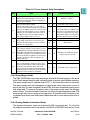
either no censorship or information censorship without modifying the CMF array
contents. Cleared censorship will prevent CMF array accesses when the device
is censored and ACCESS = 0.
• Erase interlock write — A write to any CMF array address after initializing the
erase sequence.
• Erase margin read — Special off-page read of the CMF array where the CMF
EEPROM hardware adjusts the reference of the sense amplifier to check for correct erase operation. All CMF array off-page read accesses between the erase
interlock write and clearing the SES bit are erase margin reads.
• Information censorship — CENSOR[0:1] = 11. Requires an erase of the CMF
EEPROM to change CENSOR[0:1]. Information censorship will prevent CMF array accesses when the device is censored and ACCESS = 0. Information stored
in the CMF array is made invalid while clearing CENSOR[0:1].
• Initialize program/erase sequence — The write to the high voltage control register that changes the SES bit from a zero to a one.
• MoneT — The CMF EEPROM’s FLASH bit cell.
• No censorship — CENSOR[0:1] = 10 or 01, The CMF EEPROM can change to
information censorship without modifying the CMF array contents. No censorship
allows all CMF array accesses.
• Off-page read — Array read operation that requires two clocks and updates a
page buffer.
• On-page read — Array read operation that accesses information in one of the
read page buffers and requires one clock.
• Over-programmed — By exceeding the specified programming time and/or voltage a CMF bit may be over-programmed. This bit will cause erased bits on the
same column in the same array block to read as programmed.
• Programming write — A word write to a CMF array address to transfer information into a program page buffer. The CMF EEPROM accepts programming writes
from after initializing the program sequence until the EHV bit is changed from a
zero to a one.
• Program margin read — Special off-page read of the CMF array where the CMF
EEPROM hardware adjusts the reference of the sense amplifier to check for correct program operation. All CMF array off-page read accesses between the first
programming write and clearing the SES bit are program margin reads.
• Program page buffer — 64 bytes of information used to program the CMF array.
This information is aligned to a 64-byte boundary within the CMF array block.
Each CMF module has one program page buffer for each array block.
• Read page buffer — 32-byte block of information that is read from the CMF array. This information is aligned to a 32-byte boundary within the CMF array. Each
CMF module has two read page buffers.
• Shadow information — An extra row (256 bytes) of the CMF array used to provide reset configuration information. This row may be accessed by setting the SIE
bit in the module configuration register and accessing the CMF array. The shadow information is always in the lowest array block of the CMF array.
MPC555 / MPC556
CDR MoneT FLASH EEPROM
USER’S MANUAL
Rev. 15 October 2000
MOTOROLA
19-3