1
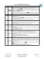
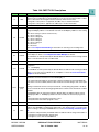
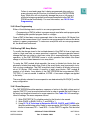
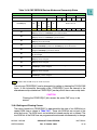
Table 19-2 CMFMCR Bit Descriptions (Continued)
Bit(s)
16:23
Name
Description
Data space. Each array block can be mapped into data or both data and Instruction address
space. When an array block is mapped into data address space (DATA[M] = 1) only data accesses are allowed. An instruction access to a location in data address space will result in a data
error exception. When an array block is mapped into both data and instruction address space
DATA[0:7] (DATA[M] = 0), both data and instruction accesses are allowed.
The DATA[0:7] bits are write protected by the LOCK and CSC bits. Writes have no effect if LOCK
= 0 or CSC = 1.
0 = Array block M is placed in both data and instruction address spaces (reset value)
1 = Array block M is placed in data address space
Block protect. Each array block of the CMF EEPROM can be protected from program and erase
operation by setting PROTECT[M] = 1. The CMF BIU will perform all programming and erase
interlocks except the program and erase voltages will not be applied to MoneT locations within
the protected array block(s).
24:31
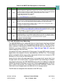
PROTECT Writes to PROTECT[0:7] have no effect if LOCK = 0 or CSC = 1 or SES = 1.
[0:7]
0 = Array block M is unprotected
1 = Array block M is protected (default value)
Warning: If a CMF EEPROM enables the lock protection mechanism (LOCK = 0) before
PROTECT is cleared, the device must use background debug mode to program or erase the
CMF EEPROM.
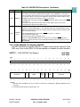
19.2.1.2 CMF EEPROM Test Register (CMFTST)
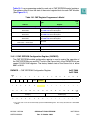
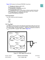
The CMF EEPROM test register (CMFTST) is used to control the test operation of the
CMF array. Only six bits [20:23, 25:26] are readable or writeable in normal operation.
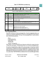
CMFTST — CMF EEPROM Test Register
MSB
0
1
2
3
4
5
6
7
0x2F C804
0x2F C844
8
9
10
11
12
13
14
15
0
RESERVED
RESET:
0
0
0
0
0
0
0
0
0
0
0
0
0
0
0
16
17
18
19
20
21
22
23
24
25
26
27
28
29
30
LSB
31
0
0
NVR1
RESERVED
RESERVE STE1,2
D
PAWS
GDB1
RESERVED
RESET:
0
0
0
0
0
0
0
0
0
0
0
0
0
0
NOTES:
1. The NVR, STE, and GDB bits are not accessible in all revisions of the MPC555 / MPC556 (2K02A mask sets
and earlier).
2. The STE bit should always be programmed as a 0.
MPC555 / MPC556
CDR MoneT FLASH EEPROM
USER’S MANUAL
Rev. 15 October 2000
MOTOROLA
19-7