1
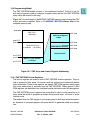
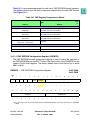
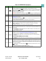
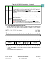
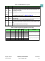
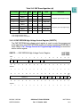
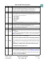
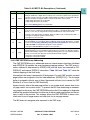
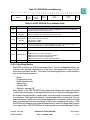
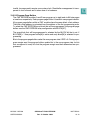
SECTION 19
CDR MoneT FLASH EEPROM
19.1 Introduction
The two CDR MoneT flash EEPROM modules (CMF) serve as electrically programmable and erasable non-volatile memory (NVM) to store system program and data.
The modules are designed to be used with the unified bus (U-bus). The CMF arrays
use Motorola’s one-transistor (MoneT) bit cell technology. The MPC555 / MPC556’s
total 448-Kbytes of flash EEPROM non-volatile memory are distributed between two
CMF EEPROM modules: a 256-Kbyte array and a 192-Kbyte array. The erase block
size is 32 Kbytes.
Each CMF EEPROM module is arranged into two major sections. The first section is
the flash EEPROM array used to store system program and data. The second section
is the bus interface unit (BIU) that controls access and operation of the array through
a standard U-bus interface and the external signals EPEE (external program or erase
enable) and VPP (supply program or erase power).
Each CMF EEPROM module array is divided into blocks to allow for independent
erase, access state, and protection from program and erase for each block. Information is transferred to the CMF EEPROM through the U-bus a word (32 bits), half-word
(16 bits), or byte at a time.
The BIU accesses 32 bytes of information in the array at a time. These bytes are copied into a read-page buffer aligned to the low order addresses, ADDR[27:31]. Each
CMF module contains two non-overlapping page buffers. The first page buffer is associated with array blocks zero to three. The second page is associated with array
blocks four to seven (for CMF Module A), or blocks four to five (for CMF Module B).
Read access time for data in the page buffers (on-page read) is one system clock. The
read access time for a new page of data (off-page read) is two system clocks. To prevent the BIU from accessing an unnecessary page from the array, the CMF EEPROM
monitors the U-bus address to determine whether the required information is in one of
the two current pages and whether the access is valid for the module.
Burst accesses are not supported by the CMF EEPROM. In normal operation, write
accesses to the CMF array are not recognized.
The CMF EEPROM module requires an external program or erase voltage (VPP) to
program or erase the array or any of its control register shadow bits. Special hardware
interlocks and the external signal EPEE protect the array from accidental enabling of
program and erase operation. The program and erase algorithms are implemented by
a series of writes to the CMF EEPROM registers and are under software control.
MPC555 / MPC556
CDR MoneT FLASH EEPROM
USER’S MANUAL
Rev. 15 October 2000
MOTOROLA
19-1
Up to eight unique 64-byte pages are programmed simultaneously in eight separate
array blocks of each of the two CMF modules. Each of the pages being programmed
simultaneously is located at the same block offset address, ADDR[17:25].
Erasing is performed on one or more of the selected block(s) simultaneously.
19.1.1 MPC555 / MPC556 CMF Features
• Motorola’s one-transistor (MoneT) bit cell
• Reset configuration stored in special FLASH NVM locations
• Array sizes of 256 Kbytes and 192 Kbytes
• Arrays distributed in 32-Kbyte blocks
— Erase by block(s)
— Block protection for program and erase operations
— Block access state control
• Select between supervisor and supervisor/user spaces
• Select between data and instruction/data spaces
— 32-bit word length
• Page mode read
— Retains two separate pages per CMF module
— Page size of 32 bytes (eight words)
— Off-page read access time of two system clocks
— On-page read access time of one system clock
• Supports U-bus pipelined accesses to a pipe depth of two
• Program up to 512 bytes at a time per CMF module
— Program up to eight unique 64-byte pages of data in eight separate blocks simultaneously (CMF Module A)
— Program up to six unique 64-byte pages of data in six separate blocks simultaneously (CMF Module B)
— Program CMF Module A and CMF Module B at the same time
— Pages located at the same offset address
• Self-timed program and erase pulses
— Internal pulse width timing control generates pulses from 4.00 µs to 2.73 s using system clock frequencies from 8.0 MHz to 40.0 MHz
• Censored access mode with a user bypass for uncensored access per CMF module
• External 4.75 to 5.25-V VPP program and erase power supply
• External program or erase enable signal (EPEE)
• CMF arrays are hardware mapped to the first 512 Kbytes of the 4-Mbyte internal
address space of the U-bus
• Supports external emulation
19.1.2 Glossary of Terms for the CMF EEPROM
• Array block — 32-Kbyte contiguous block of information. Each array block may
be erased independently.
• BIU — Bus interface unit controls access and operation of the CMF array through
a standard U-bus interface.
• Cleared censorship — CENSOR[0:1] = 00. The CMF EEPROM can change to
MPC555 / MPC556
CDR MoneT FLASH EEPROM
USER’S MANUAL
Rev. 15 October 2000
MOTOROLA
19-2
either no censorship or information censorship without modifying the CMF array
contents. Cleared censorship will prevent CMF array accesses when the device
is censored and ACCESS = 0.
• Erase interlock write — A write to any CMF array address after initializing the
erase sequence.
• Erase margin read — Special off-page read of the CMF array where the CMF
EEPROM hardware adjusts the reference of the sense amplifier to check for correct erase operation. All CMF array off-page read accesses between the erase
interlock write and clearing the SES bit are erase margin reads.
• Information censorship — CENSOR[0:1] = 11. Requires an erase of the CMF
EEPROM to change CENSOR[0:1]. Information censorship will prevent CMF array accesses when the device is censored and ACCESS = 0. Information stored
in the CMF array is made invalid while clearing CENSOR[0:1].
• Initialize program/erase sequence — The write to the high voltage control register that changes the SES bit from a zero to a one.
• MoneT — The CMF EEPROM’s FLASH bit cell.
• No censorship — CENSOR[0:1] = 10 or 01, The CMF EEPROM can change to
information censorship without modifying the CMF array contents. No censorship
allows all CMF array accesses.
• Off-page read — Array read operation that requires two clocks and updates a
page buffer.
• On-page read — Array read operation that accesses information in one of the
read page buffers and requires one clock.
• Over-programmed — By exceeding the specified programming time and/or voltage a CMF bit may be over-programmed. This bit will cause erased bits on the
same column in the same array block to read as programmed.
• Programming write — A word write to a CMF array address to transfer information into a program page buffer. The CMF EEPROM accepts programming writes
from after initializing the program sequence until the EHV bit is changed from a
zero to a one.
• Program margin read — Special off-page read of the CMF array where the CMF
EEPROM hardware adjusts the reference of the sense amplifier to check for correct program operation. All CMF array off-page read accesses between the first
programming write and clearing the SES bit are program margin reads.
• Program page buffer — 64 bytes of information used to program the CMF array.
This information is aligned to a 64-byte boundary within the CMF array block.
Each CMF module has one program page buffer for each array block.
• Read page buffer — 32-byte block of information that is read from the CMF array. This information is aligned to a 32-byte boundary within the CMF array. Each
CMF module has two read page buffers.
• Shadow information — An extra row (256 bytes) of the CMF array used to provide reset configuration information. This row may be accessed by setting the SIE
bit in the module configuration register and accessing the CMF array. The shadow information is always in the lowest array block of the CMF array.
MPC555 / MPC556
CDR MoneT FLASH EEPROM
USER’S MANUAL
Rev. 15 October 2000
MOTOROLA
19-3
19.2 Programming Model
The CMF EEPROM Module consists of two addressed sections. The first is the 32byte control registers used to configure, program, erase and test the CMF EEPROM
array while, the second is the array.
Figure 19-1 shows the part of the MPC555 / MPC556 memory map involving the CMF
arrays and control registers. Refer to 1.3 MPC555 / MPC556 Address Map for the
complete memory map.
0x00 0000
CMF Flash
448 Kbytes
0x2F C000
USIU Control Registers
1 Kbyte
0x06 FFFF
0x08 0000
FLASH Module A (64 bytes)
Reserved for Flash
(2.6 Mbytes – 16 Kbytes)
FLASH Module B (64 bytes)
0x2F C800
0x2F C840
0x2F C880
Reserved for SIU
0x 2F BFFF
0x 2F C000
0x 2F FFFF
U SI U & F lash Control
16 Kbytes
Figure 19-1 CMF Array and Control Register Addressing
19.2.1 CMF EEPROM Control Registers
The control registers are used to control CMF EEPROM module operation. They reside in supervisor data space. On master reset the registers are loaded with default
reset information. Some of the registers are special CMF NVM registers which retain
their state when power is removed from the CMF EEPROM. These special FLASH
NVM registers are identified in the individual register field and control bit descriptions.
The CMF EEPROM control registers are accessible for read or write operation at all
times while the device is powered up except during master reset, soft reset or erase
interlock write.
The access time of a CMF register is one system clock for both read and write accesses. Accesses to reserved registers will cause the BIU to generate a data error exception.
MPC555 / MPC556
CDR MoneT FLASH EEPROM
USER’S MANUAL
Rev. 15 October 2000
MOTOROLA
19-4
Table 19-1 is a programming model for each set of CMF EEPROM control registers.
The address offset is from the start of the control register block for each CMF module.
(See Figure 19-1.)
Table 19-1 CMF Register Programmer’s Model
MSB
0
Address
LSB
31
Register
Control Registers (Located in Supervisor Data Space)
0x2F C800
0x2F C840
CMF Module Configuration Register (CMFMCR)
See Table 19-2 for bit descriptions.
0x2F C804
0x2F C844
CMF EEPROM Test Register (CMFTST)
See Table 19-3 for bit descriptions.
0x2F C808
0x2F C848
High Voltage Control Register (CMFCTL)
See Table 19-6 for bit descriptions.
0x2F C80C — 0x2F C81C
0x2F C84C — 0x2F C85C
Reserved
CMF Flash Array
0x00 0000 – 0x03 FFFF
CMF_A RAM Array
0x04 0000 – 0x06 FFFF
CMF_B RAM Array
19.2.1.1 CMF EEPROM Configuration Register (CMFMCR)
The CMF EEPROM module configuration register is used to control the operation of
the CMF EEPROM array and BIU. Two bits (the Censor bits) of the CMFMCR bits are
special FLASH NVM registers. The factory default state of the Censor bits is either
0b01 or 0b10.
CMFMCR — CMF EEPROM Configuration Register
MSB
0
1
2
3
4
5
LOCK
0
0
FIC
SIE
ACCESS
6
7
8
0x2F C800
0x2F C840
9
10
CENSOR1
11
12
13
14
15
SUPV[0:7]
RESET:
1
0
0
0
0
0
16
17
18
19
20
21
22
23
1
1
1
1
1
1
1
1
24
25
26
27
28
29
30
LSB
31
1
1
1
DATA[0:7]
PROTECT[0:7]
RESET:
0
0
0
0
0
0
0
0
1
1
1
1
1
1. The reset state of bits 6:7 are defined by special FLASH NVM registers. The factory default state is either 0b01
or 0b10.
MPC555 / MPC556
CDR MoneT FLASH EEPROM
USER’S MANUAL
Rev. 15 October 2000
MOTOROLA
19-5
Table 19-2 CMFMCR Bit Descriptions
Bit(s)
Name
Description
Lock control. When the LOCK control bit is cleared, the following bits are locked: FIC,
SUPV[0:7], DATA[0:7] and PROTECT[0:7]. Writes to these bits will have no effect.
0
LOCK
In normal operation, once the LOCK bit is cleared, the write-lock can only be disabled again by
a master reset. The LOCK bit is writable if the device is in background debug mode and CSC = 0.
0 = Write-locked registers are protected
1 = Write-lock is disabled (reset state)
Warning: If the lock protection mechanism is enabled (LOCK = 0) before the PROTECT[0:7] bits
are cleared, the device must use background debug mode to program or erase the CMF array.
1:2
—
Reserved
Force information censorship for access development. Refer to 19.8 Censored and Non-Censored Accesses for details.
3
FIC
The FIC bit is write protected by the LOCK. If FIC = 1 it cannot be cleared except by a hard reset.
0 = Normal CMF censorship operation
1 = Forces the CMF into information censorship mode, unless ACCESS = 1
Shadow information enable. Refer to 19.3 Shadow Information for details.
4
SIE
The SIE bit is write protected by the SES bit for programming operation. Writes have no effect
if (SES = 1 and PE = 0). The SIE bit can be read whenever the registers are enabled.
0 = Normal array access
1 = Disables normal array access and selects the shadow information
Enable uncensored access. Refer to 19.8 Censored and Non-Censored Accesses for details.
5
ACCESS
Writes to this bit have no effect when CSC = 1. This bit can be set only when the MCU is in uncensored mode.
0 = Censored CMF array access allowed only if the CMF censorship is no censorship, (FIC = 0
and CENSOR[0] ≠ CENSOR[1])
1 = Allows all CMF array access.
Censor accesses. The value of these bits is determined by the state of two NVM bits in two special NVM fuses. Refer to 19.8 Censored and Non-Censored Accesses for details.
6:7
8:15
The default reset state of CENSOR is user defined by the FLASH NVM register bits.
00 = Cleared censorship, CMF array access allowed only if device is in uncensored mode or
CENSOR
ACCESS = 1
01 = No censorship, All CMF array accesses allowed
10 = No censorship, All CMF array accesses allowed
11 = Information censorship, CMF array access allowed only if device is in uncensored mode or
ACCESS = 1
Supervisor space. Each array block can be mapped into supervisor or unrestricted address
space. When an array block is mapped into supervisor address space, only supervisor accesses
are allowed. A user access to a location in supervisor address space will result in a data error
exception. When an array block is mapped into unrestricted address space, both supervisor and
SUPV[0:7] user accesses are allowed.
The SUPV[0:7] bits are write protected by the LOCK and CSC bits. Writes will have no effect if
LOCK=0 or CSC=1.
0 = Array block M is placed in unrestricted address space
1 = Array block M is placed in supervisor address space (reset value)
MPC555 / MPC556
CDR MoneT FLASH EEPROM
USER’S MANUAL
Rev. 15 October 2000
MOTOROLA
19-6
Table 19-2 CMFMCR Bit Descriptions (Continued)
Bit(s)
16:23
Name
Description
Data space. Each array block can be mapped into data or both data and Instruction address
space. When an array block is mapped into data address space (DATA[M] = 1) only data accesses are allowed. An instruction access to a location in data address space will result in a data
error exception. When an array block is mapped into both data and instruction address space
DATA[0:7] (DATA[M] = 0), both data and instruction accesses are allowed.
The DATA[0:7] bits are write protected by the LOCK and CSC bits. Writes have no effect if LOCK
= 0 or CSC = 1.
0 = Array block M is placed in both data and instruction address spaces (reset value)
1 = Array block M is placed in data address space
Block protect. Each array block of the CMF EEPROM can be protected from program and erase
operation by setting PROTECT[M] = 1. The CMF BIU will perform all programming and erase
interlocks except the program and erase voltages will not be applied to MoneT locations within
the protected array block(s).
24:31
PROTECT Writes to PROTECT[0:7] have no effect if LOCK = 0 or CSC = 1 or SES = 1.
[0:7]
0 = Array block M is unprotected
1 = Array block M is protected (default value)
Warning: If a CMF EEPROM enables the lock protection mechanism (LOCK = 0) before
PROTECT is cleared, the device must use background debug mode to program or erase the
CMF EEPROM.
19.2.1.2 CMF EEPROM Test Register (CMFTST)
The CMF EEPROM test register (CMFTST) is used to control the test operation of the
CMF array. Only six bits [20:23, 25:26] are readable or writeable in normal operation.
CMFTST — CMF EEPROM Test Register
MSB
0
1
2
3
4
5
6
7
0x2F C804
0x2F C844
8
9
10
11
12
13
14
15
0
RESERVED
RESET:
0
0
0
0
0
0
0
0
0
0
0
0
0
0
0
16
17
18
19
20
21
22
23
24
25
26
27
28
29
30
LSB
31
0
0
NVR1
RESERVED
RESERVE STE1,2
D
PAWS
GDB1
RESERVED
RESET:
0
0
0
0
0
0
0
0
0
0
0
0
0
0
NOTES:
1. The NVR, STE, and GDB bits are not accessible in all revisions of the MPC555 / MPC556 (2K02A mask sets
and earlier).
2. The STE bit should always be programmed as a 0.
MPC555 / MPC556
CDR MoneT FLASH EEPROM
USER’S MANUAL
Rev. 15 October 2000
MOTOROLA
19-7
Table 19-3 CMFTST Bit Descriptions
Bit(s)
Name
0:19
—
Description
Reserved
20
NVR
Negative voltage range. This bit switches between the low and high voltage range of the negative charge pump in programming and erasing the CMF Flash module when GDB = 0b1. This
bit is writeable when HVS = 0b0.
0 = High Range (more negative)
1 = Low Range
21:23
PAWS
[0:2]
Program amplitude/width modulation select. The PAWS bits, in conjunction with the NVR and
GDB bits can be used to select the programming voltage applied to the drain or gate of the EEPROM bitcell. These bits should be left set to 0b000, unless advised by Motorola. For information about PAWS programming modes, see Table 19-4 and Table 19-5.
24
—
Reserved
STE
This bit is reserved for Motorola factory testing and should always be programmed to 0b0.
0 = Normal Operation
1 = Factory test mode use only. This setting could disturb contents of flash.
26
GDB
Gate/drain bias select. This bit works in conjunction with the PAWS bits to select between positive and negative ramped voltages for programing and erasing. This bit is writeable when SES
= 0b0.
0 = Positive voltage ramp selected on the bitcell drain.
1 = Negative voltage ramp selected on the bitcell gate.
27:31
—
25
Reserved
Table 19-4 CMF Programming Algorithm (v6 and Later)
No. of Pulses
Pulse Width
NVR
PAWs
GDB
PAWs
Mode
4
256 µs
1
100
1
Mode 4NL
4
256 µs
1
101
1
Mode 5NL
4
256 µs
1
110
1
Mode 6NL
4
256 µs
1
111
1
Mode 7NL
20
50 µs
0
100
1
Mode 4NL
20
50 µs
0
101
1
Mode 5NL
20
50 µs
0
110
1
Mode 6NL
max. 48,000
50 µs
0
111
1
Mode 7NL
MPC555 / MPC556
CDR MoneT FLASH EEPROM
USER’S MANUAL
Rev. 15 October 2000
Description
Negative gate ramp (low range)
Negative gate ramp (high range)
MOTOROLA
19-8
Table 19-5 CMF Erase Algorithm (v6)
No. of Pulses
Pulse Width
NVR
PAWs
GDB
PAWs
Mode
1
100 ms1
1
100
1
Mode 4NL
1
100 ms1
1
101
1
Mode 5NL
1
100 ms1
1
110
1
Mode 6NL
1
100 ms1
1
111
1
Mode 7NL
1
100 ms1
0
100
1
Mode 4NL
1
100 ms1
0
101
1
Mode 5NL
1
100 ms1
0
110
1
Mode 6NL
20
100 ms2
0
111
1
Mode 7NL
Description
Negative gate ramp (low range)
Negative gate ramp (high range)
NOTES:
1. No margin read after pulse.
2. Do margin read after each pulse.
19.2.1.3 CMF EEPROM High Voltage Control Register (CMFCTL)
The CMF EEPROM high voltage control register is used to control the program and
erase operations of the CMF EEPROM module and setting and clearing CENSOR[0:1]
fuses. Refer to 19.7 Voltage Control for Programming and Erasing for more information on this register.
CMFCTL — CMF EEPROM High Voltage Control Register
MSB
0
1
HVS
0
2
3
4
SCLKR
5
0
6
7
CLKPE
8
9
10
0x2F C808
0x2F C848
11
0
12
13
14
15
CLKPM
PORESET/HRESET:
0
0
0
0
0
0
0
0
0
0
0
0
0
0
0
0
U
U
U
U
U
U
U
U
U
U
U
U
U
U
U
U
16
17
18
19
20
21
22
23
24
25
26
27
28
29
30
LSB
31
0
CSC
EPEE
0
0
PE
SES
EHV
SRESET:
BLOCK[0:7]
PORESET/HRESET:
0
0
0
0
0
0
0
0
0
0
0
0
0
0
0
0
U
U
U
U
U
U
U
U
U
U
U
U
U
U
U
SRESET:
U
MPC555 / MPC556
CDR MoneT FLASH EEPROM
USER’S MANUAL
Rev. 15 October 2000
MOTOROLA
19-9
Table 19-6 CMFCTL Bit Descriptions
Bit(s)
Name
Description
0
HVS
High voltage status. During a program or erase pulse this bit is set while the pulse is active or
during recovery. The BIU does not acknowledge an access to an array location if HVS = 1. While
HVS = 1, SES cannot be changed. This bit is read only; writes have no effect.
0 = Program or erase pulse is not applied to the CMF array or shadow information
1 = Program or erase pulse is applied to the CMF array or shadow information
1
—
2:4
SCLKR
Reserved
System clock range. These bits are write protected by the SES bit. Writes to CMFCTL do not
change SCLKR[0:2] if SES = 1. The default reset state of SCLKR[0:2] = 000 for a clock scaling
of 1.
000 = Clock scaling of 1 (Not for Customer use.)
001 = Clock scaling of 1
010 = Clock scaling of 3/2
011 = Clock scaling of 2
100 = Clock scaling of 3
101 = Clock scaling of 4
110 = Reserved
111 = Reserved
Refer to 19.7.3 System Clock Scaling for instructions on selecting a clock scaling factor.
5
—
6:7
CLKPE
8
—
9:15
CLKPM
Reserved
Clock period exponent. The CLKPE, CSC, and PE fields determine the value of the exponential
clock multiplier, N. Refer to 19.7.4 Exponential Clock Multiplier for details.
The CLKPE bits are write protected by the SES bit. Writes to CMFCTL will not change CLKPE
if SES = 1.The default reset state of CLKPE is 00.
Reserved
Clock period multiple. This field determines the linear clock multiplier, M, according to the following equation:
M = 1 + CLKPM[0:6]
The CLKPM bits are write protected by the SES bit. Writes to CMFCTL will not change CLKPM
if SES = 1. The reset state of CLKPM = 0, for a multiplier of 1. Refer to 19.7.5 Linear Clock
Multiplier for more information.
Block program and erase select. The CMF EEPROM array blocks that are selected to be programmed or erased are the blocks for which BLOCK[M] = 1.
Bit 16 controls block 0 and bit 23 controls block 7. On the 192-Kbyte array (Flash Module B),
blocks 6 and 7 are not available, but these bits need to be set when doing a clear censor operation.
16:23
BLOCK
[0:7]
Warning: The block bit must be set only for the blocks currently being programed. If the block
bits are set for blocks that are not being programmed, the contents of the other blocks could be
disturbed.
The BLOCK[0:7] bits are write protected by the SES bit. Writes to CMFCTL will not change
BLOCK[0:7] if SES = 1. BLOCK[0:7] default reset state is 0x00, not selected for program or
erase.
0 = Array block M is not selected for program or erase
1 = Array block M is selected for program or erase
24
25
—
CSC
Reserved
Censor set or clear. CSC configures the CMF EEPROM for setting or clearing the CENSOR bits.
If CSC=1 then CENSOR is configured for setting if PE = 0 or clearing if PE = 1. For more information on setting or clearing the CENSOR bits see section 19.8.4 Setting and Clearing Censor.
The CSC bit is write protected by the SES bit. Writes to CMFCTL will not change CSC if SES = 1.
0 = Configure for normal operation (default value)
1 = Configure to set or clear the CENSOR bits
MPC555 / MPC556
CDR MoneT FLASH EEPROM
USER’S MANUAL
Rev. 15 October 2000
MOTOROLA
19-10
Table 19-6 CMFCTL Bit Descriptions (Continued)
Bit(s)
26
Name
EPEE
Description
EPEE pin status bit. The EPEE bit monitors the state of the external program/erase enable
(EPEE) pin. EPEE has a digital filter that requires two consecutive samples to be equal before
the output of the filter changes. The CMF samples EPEE when EHV is asserted and holds the
EPEE state until EHV is negated. EPEE is a read-only bit; writes have no effect.
0 = High voltage operations are not possible
1 = High voltage operations are possible
Refer to 19.9.1 EPEE Signal for more information.
27:28
29
30
31
—
PE
Reserved
Program or erase select. PE configures the CMF EEPROM for programming or erasing. When
PE = 0, the array is configured for programming and if SES = 1 the SIE bit will be write locked.
When PE = 1, the array is configured for erasing and SES will not write lock the SIE bit.
The PE bit is write protected by the SES bit. Writes to CMFCTL will not change PE if SES = 1.
0 = Configure for program operation (default value)
1 = Configure for erase operation
SES
Start-end program or erase sequence. The SES bit is write protected by the HVS and EHV bits,
unless the PAW bits are set to 0b1xx. Writes to CMFCTL will not change SES if HVS = 1 or EHV
= 1. Refer to 19.7.7 Starting and Ending a Program or Erase Sequence for more information.
0 = CMF EEPROM not configured for program or erase operation
1 = Configure CMF EEPROM for program or erase operation
EHV
Enable high voltage. EHV can be asserted only after the SES bit has been asserted and a valid
programming write(s) or erase hardware interlock write has occurred. If an attempt is made to
assert EHV when SES is negated, or if a valid programming write(s) or erase hardware interlock
write has not occurred since SES was asserted, EHV will remain negated.
0 = Program or erase pulse disabled
1 = Program or erase pulse enabled
19.2.2 CMF EEPROM Array Addressing
The CMF EEPROM array is addressed when an internal access has been initialized
and ADDR[10:13] matches the array hardware mapping address. The CMF array location selected is determined by ADDR[14:29] and the bytes are selected by ADDR[30:31] and internal SIZE[0:1] information. Table 19-6 and Table 19-7 show the
internal mapping of the flash array.
Information in the array is accessed in 32-byte pages. For each CMF module, two read
page buffers are assigned to the low order addresses (ADDR[27:31]). The first page
buffer is assigned to blocks zero to three; the second to blocks four to seven (for CMF
Module A) or four to five (for CMF Module B).
Access time for data in the read page buffers is one system clock; access time for an
off-page read is two system clocks. To prevent the BIU from accessing an unnecessary page from the array, the CMF EEPROM monitors the U-bus address to determine
whether the required information is within one of the two read page buffers and the access is valid for the module. This strategy allows the CMF EEPROM to have a twoclock read for an off-page access and one clock for an on-page access.
The BIU does not recognize write accesses to the CMF array.
MPC555 / MPC556
CDR MoneT FLASH EEPROM
USER’S MANUAL
Rev. 15 October 2000
MOTOROLA
19-11
Table 19-7 EEPROM Array Addressing
0
1
2
3
4
5
6
7
8
9
USIU
Internal
Mapping
0000000
1
0
1
1
1
2
Array
Hardware
Mapping
1
3
1
4
1
5
1
6
1
7
1
8
Block
Address
1
9
2
0
2
1
2
2
2
3
2
4
2
5
Row
Address
2
6
2
7
Column
Address
2
8
2
9
3
0
3
1
Byte
Addr
Table 19-8 CMF EEPROM Array Address Fields
Bit(s)
Field
0:6
—
The seven high-order address bits of a CMF EEPROM array access (or any MPC555 /
MPC556 internal access) must equal zero.
7:9
USIU Internal
Mapping
These bits (programmed in the USIU internal memory map register) specify one of eight
locations for the MPC555 / MPC556 internal memory map.
10:13
Description
These bits determine the location of each array within the MPC555 / MPC556 internal
Array Hardware memory map. Values are as follows:
Mapping
Flash module A = 0000
Flash Module B = 0001
14:16
Block Address
These three bits specify one of eight 32-Kbyte blocks within CMF Module A (000 to 111),
or one of six 32-Kbyte blocks within CMF Module B (000 to 101)
17:23
Row Address
These seven bits select one of 128 rows within the 32-Kbyte block.
24:29
30:31
These six bits select one of 64 (word-length) columns within the row. Note also the following:
Column Address ADDR[24:26] select a 32-byte read page.
ADDR[27:29] represent the read page word address.
ADDR[24:25] select a 64-byte program page.
ADDR[26:29] represent the program page word address.
Byte Address
Bits 30:31 select a byte within the column.
19.2.2.1 Read Page Buffers
Each CMF array has two 32-byte read page buffers. The fully independent buffers are
located in two separate read sections of the array. Each page buffer status and address are monitored in the BIU. The status of the read page buffers is made invalid by
any of the following operations:
• Reset
• Programming write
• Erase interlock write
• Setting EHV
• Clearing SES
• Setting or clearing SIE
Each access to the CMF EEPROM array determines whether the requested location
is within the current pages. If the requested location is not within the read page buffers,
the correct read page buffer is made invalid, and a new page of information is fetched
from the array. The page buffer address is updated and status is made valid. If the requested location is within one of the current page buffers or has been fetched from the
array, the selected bytes are transferred to the U-bus, completing the access. CMF
EEPROM array accesses that make the page buffer(s) invalid (off-page reads) require
two system clocks. CMF EEPROM array accesses that do not make the page buffer(s)
MPC555 / MPC556
CDR MoneT FLASH EEPROM
USER’S MANUAL
Rev. 15 October 2000
MOTOROLA
19-12
invalid (on-page reads) require one system clock. Read buffer management is transparent to user software and is taken care of in hardware.
19.2.2.2 Program Page Buffers
The CMF EEPROM modules A and B can program up to eight and six 64-byte pages
at one time, respectively. Each program page buffer is located in one program section.
All program page buffers within a CMF module share the same block offset address.
The block offset address is extracted from the address of the first programming write.
To select the CMF EEPROM array block that will be programmed, the program page
buffers use the CMF EEPROM array configuration and BLOCK[0:7].
The array block that will be programmed is selected by the BLOCK bit that is set. If
BLOCK[M] = 1 then program buffer[M] is active and array block[M] is selected for programming.
Bits in the program page buffers select the non-program state if SES = 0. During a program margin read, the program buffers update bits to the non-program state for bits
that correspond to array bits that the program margin read has determined are programmed.
MPC555 / MPC556
CDR MoneT FLASH EEPROM
USER’S MANUAL
Rev. 15 October 2000
MOTOROLA
19-13
19.2.2.3 Array Configuration for CMF Module A
64-byte Program Page Buffer 7
3-2Kbyte Array Block 7
0x3 8000 – 0x3 FFFF
64-byte Program Page Buffer 6
32-Kbyte Array Block 6
0x3 0000 – 0x3 7FFF
32-byte Read Page Buffer 1
32-Kbyte Array Block 5
0x2 8000 – 0x2 FFFF
64-byte Program Page Buffer 5
32-Kbyte Array Block 4
0x2 0000 – 0x2 7FFF
64-byte Program Page Buffer 4
64-byte Program Page Buffer 3
32-Kbyte Array Block 3
0x1 8000 – 0x1 FFFF
64-byte Program Page Buffer 2
32-Kbyte Array Block 2
0x1 0000 – 0x1 7FFF
32-byte Read Page Buffer 0
32-Kbyte Array Block 1
0x0 8000 – 0x0 FFFF
64-byte Program Page Buffer 1
32-Kbyte Array Block 0 and
Shadow Information
0x0 0000 – 0x0 7FFF1
64-byte Program Page Buffer 0
Bus Interface Unit (BIU)
1.If SIE=1, then the shadow row is enabled instead of the flash block.
Shadow locations 0x00 to 0x03 are reserved for the Internal Flash Reset
Configuration word. Shadow locations 0x04 to 0x0F are Reserved by
Motorola for possible future use.
MPC555 / MPC556
CDR MoneT FLASH EEPROM
USER’S MANUAL
Rev. 15 October 2000
MOTOROLA
19-14
19.2.2.4 Array Configuration for CMF Module B
64-byte Program Page Buffer 5
32-Kbyte Array Block 5
0x6 8000 – 0x6 FFFF
32-byte Read Page Buffer 1
32-Kbyte Array Block 4
0x6 0000 – 0x6 7FFF
64-byte Program Page Buffer 4
64-byte Program Page Buffer 3
32-Kbyte Array Block 3
0x5 8000 – 0x5 FFFF
64-byte Program Page Buffer 2
32-Kbyte Array Block 2 0x5 0000 – 0x5 7FFF
32-byte Read Page Buffer 0
32-Kbyte Array Block 1
0x4 8000 – 0x4 FFFF
64-byte Program Page Buffer 1
32-Kbyte Array Block 0 and
Shadow Information
0x4 0000 – 0x4 7FFF1
64-byte Program Page Buffer 0
Bus Interface Unit (BIU)
1. If SIE=1, then the shadow row is enabled instead of the flash block.
Locations 0x4 00000 to 0x4 000F of the shadow row are Reserved by
Motorola for possible future use.
19.3 Shadow Information
Programming the shadow information uses the same procedure as programming the
array, except that there are only 256 bytes available in the shadow row. Before starting
the program sequence SIE must equal one.
The SIE bit is write protected by the SES bit for programming operation. Writes will
have no effect if (SES = 1 and PE = 0). The SIE bit can be read whenever the registers
are enabled.
When SIE = 1, normal array accesses are disabled and the shadow information is enabled. When an array location is read using supervisor data in this mode, the shadow
information is read from a location determined by the column, 32-byte read page select
and read page word addresses (ADDR[24:29]) of the access. Accessing the CMF control block registers accesses the registers and not the shadow information. The read
page buffer address monitor is reset whenever SIE is modified, making the next CMF
array access an off-page access.
The default reset state of SIE is normal array access (SIE = 0).
MPC555 / MPC556
CDR MoneT FLASH EEPROM
USER’S MANUAL
Rev. 15 October 2000
MOTOROLA
19-15
NOTE
When SIE = 1, only program page buffer zero can be programmed.
All programming writes to the CMF will be directed to program page
buffer 0 if SIE = 1. In addition, the other program page buffers cannot
be accessed and will not apply any programming voltages to their
CMF array blocks while programming the shadow information.
19.3.1 Address Range of Shadow Information
The address range of the shadow information is the entire address range of the CMF
EEPROM array but the high order array addresses, ADDR[14:23], are not used to encode the location. The first 16 bytes (ADDR[24:29] = 0x00 to 0x0F) of the 256 bytes of
shadow locations are withheld by Motorola for the reset configuration word and future
applications. The remaining 240 bytes are available as supervisor data. This is shown
in Figure 19-2.
0x00
0x03
0x04
0x0F
0x10
Reset Configuration Word
Reserved for Future Applications
General-Use MoneT Shadow Information
0xFF
Figure 19-2 Shadow Information
19.3.2 Reset Configuration Word (CMFCFIG)
The CMF EEPROM reset configuration word is implemented in the first word (ADDR[24:29] = 0x00) of the special shadow locations. The reset configuration word along
with the rest of the shadow information words is located in supervisor data address
space. The purpose of the reset configuration word is to provide the system with an
alternative internal source for the reset configuration.
Note that with the exception of bit 20, the bits in the CMFCFIG are identical to those
in the USIU hard reset configuration word. Refer to 7.5.2 Hard Reset Configuration
Word for descriptions of these bits.
MPC555 / MPC556
CDR MoneT FLASH EEPROM
USER’S MANUAL
Rev. 15 October 2000
MOTOROLA
19-16
CMFCFIG — Hard Reset Configuration Word
MSB
0
1
2
3
EARB
IP
BDRV
BDIS
4
5
6
BPS
7
8
RESERVED
9
10
DBGC
11
12
DBPC ATWC
13
14
EBDF
15
Reserved
LSB
16
PRPM
17
18
SC
19
20
21
22
ETRE
FLEN
EN_
COMP
EXC_
COMP
23
24
25
26
Reserved
27
28
29
ISB
30
31
DME
During reset the HC bit (“has configuration,” bit 20) and the USIU configure the CMF
EEPROM module to provide CMFCFIG. If HC = 0 and the USIU requests internal configuration during reset the reset configuration word will be provided by CMFCFIG.
The default reset state of the CMFCFIG after an erase operation of the CMF module
A block 0 is no configuration word available (HC = 1).
19.4 Array Read Operation
The CMF EEPROM array is available for read operation under most conditions while
the device is powered up. Reads of the array are not allowed under any of the following
conditions:
• During master or soft reset
• ACCESS = 0 and CENSOR[0:1] = 11 or 00
• While the CMF EEPROM is disabled
During programming and erase operations, while the high voltage is applied to the array, the BIU does not acknowledge a CMF array read. At certain points, as defined in
the program or erase sequence, reading the array results in a margin read. These margin reads return the status of the program or erase operation and not the data in the
array.
The type of CMF EEPROM array read is determined by comparing the address of the
requested information with the address of the read page buffers. If the requested address is not within one of the read page buffers or if the read page buffer has been
made invalid, an off-page read results. This read updates the read page buffer address
of the selected array block, copies the information from the array into the read page
buffer, and drives a word onto the data bus. The off-page read requires a minimum of
two clocks, while margin off-page reads require additional clocks.
If the address of the requested information is within the address ranges of either of the
read page buffers, an on-page read is performed. This requires one clock to transfer
information from the read page buffer onto the data bus. See section 19.2.2 CMF EEPROM Array Addressing for more information on array accesses.
MPC555 / MPC556
CDR MoneT FLASH EEPROM
USER’S MANUAL
Rev. 15 October 2000
MOTOROLA
19-17
19.5 Programming the CMF Array
To modify the charge stored in the isolated element of the CMF bit from a logic one
state to a logic zero state, a programming operation is required. This programming
operation applies the required voltages to change the charge state of the selected bits
without changing the logic state of any other bits in the CMF array. The program operation cannot change the logic zero state to a logic one state; this must be done by the
erase operation. Programming uses a set of program buffers of 64 bytes each to store
the required data, an address offset buffer to store the starting address of the block(s)
to be programmed and a block select buffer that stores information on which block(s)
are to be programmed. Any number of the array blocks may be programmed at one
time.
WARNING
Do not program any page more than once after a successful erase
operation. While this will not physically damage the array it will cause
an increased partial disturb time for the unselected bits on the row
and columns that are not programmed. If this happens, a full erase of
all blocks being programmed must be done before the CMF
EEPROM can be used reliably.
If block M of the CMF EEPROM is protected (PROTECT[M] = 1), it will not be programmed. Also, if EPEE = 0, no programming voltages will be applied to the array.
Software should verify the state of EPEE prior to programming (programming will fail
if EPEE = 0). The user should also insure that the programming voltage (5.0 ± 0.25
volts) is applied to VPP.
19.5.1 Program Sequence
The CMF EEPROM module requires a sequence of writes to the high voltage control
register (CMFCTL) and to the programming page buffer(s) in order to enable the high
voltage to the array or shadow information for program operation. See Table 19-4 for
the programming algorithm bit settings.
The required program sequence follows.
1. Write PROTECT[0:7] to disable protection on blocks to be programmed.
2. Write PAWS to 0b100, write NVR = 1, write GDB = 1.
3. Using 19.7.6 A Technique to Determine SCLKR, CLKPE, and CLKPM, program the following fields:
— Pulse width timing control fields for a program pulse
— BLOCK[0:7] to select the array blocks to be programmed
— PE = 0 in the CMFCTL register
4. Write SES = 1 in the CMFCTL register.
NOTE
Step 4 can be accomplished with the same write as that in step 3. It
is listed as a separate step in the sequence for looping.
MPC555 / MPC556
CDR MoneT FLASH EEPROM
USER’S MANUAL
Rev. 15 October 2000
MOTOROLA
19-18
5. Write to the 64-byte array locations to be programmed. This updates the programming page buffer(s) with the information to be programmed. The last write
to a word within the program page buffer will be saved for programming. All accesses of the array after the first write are to the same block offset address
(ADDR[17:25]) regardless of the address provided. Thus the locations accessed after the first programming write are limited to the page locations to be programmed. Off-page read accesses of the CMF array after the first programming
write are program margin reads. (See section 19.5.2 Program Margin Reads.)
To select the CMF EEPROM array block(s) to be programmed, the program
page buffers use the CMF EEPROM array configuration and BLOCK[0:7]. Subsequent writes fill in the programming page buffers using the block address to
select the program page buffer and the page word address (ADDR[26:29]) to
select the word in the page buffer.
6. Write EHV = 1 in the CMFCTL register.
NOTE
If a program buffer word has not received a programming write no
programming voltages will be applied to the drain of the corresponding word in the array. Also, at this point writes to the program page
buffers are disabled until SES has been cleared and set.
7. Read the CMFCTL register until HVS = 0.
8. Write EHV = 0.
9. To verify the programming, read the words of the pages that are being programmed. These are program margin reads. (See 19.5.2 Program Margin
Reads.) If any bit is a 1 after reading all of the locations that are being programmed, then another pulse needs to be applied to the these locations. If all
the locations verify as programmed go to step 11.
WARNING
After a program pulse, read at least one location with ADDR[26] = 0
and one location with ADDR[26] = 1 on each programmed page. Failure to do so may result in the loss of information in the CMF
EEPROM array. While this will not physically damage the array a full
erase of all blocks being programmed must be done before the CMF
EEPROM can be used reliably. For more information see 19.5.3
Over-Programming.
To reduce the time for verification, read two locations in each program page that
is being programmed after reading a non-programmed bit. The first location
must be a location with ADDR[26] = 0, while the second must use ADDR[26] =
1. In addition, after a location has been fully verified (all bits are programmed)
it is not necessary to verify the location again, since no further programming
voltages will be applied to the drain of the corresponding bits. This will reduce
the time required to program the array.
MPC555 / MPC556
CDR MoneT FLASH EEPROM
USER’S MANUAL
Rev. 15 October 2000
MOTOROLA
19-19
10. If the margin read is successful, then write SES = 0 in the CMFCTL register,
otherwise do the following:
a. Write new pulse width parameters (if required per Table 19-4) - SCLKR,
CLKPE, CLKPM.
b. Write new values for PAWS, NVR, and GDB (if required per Table 19-4).
c. Go back to step 6 to apply additional programming pulses.
11. If more information needs to be programmed, go back to step 2.
T3
S2
T1
S3
T2
Reset
S1
T4
T6
S4
T7
T8
T9
T5
S5
Figure 19-3 Program State Diagram
MPC555 / MPC556
CDR MoneT FLASH EEPROM
USER’S MANUAL
Rev. 15 October 2000
MOTOROLA
19-20
Table 19-9 Program Interlock State Descriptions
State
Next
State
Mode
Transition Requirement
Normal Operation:
S1
Normal array reads and register accesses. The
block protect information and pulse width timing
control can be modified.
S2
T2
Write PE = 0, SES = 1
S1
T1
Write SES = 0 or a master reset
Hardware Interlock
First Program Hardware Interlock Write:
S2
S3
S4
A successful write to any CMF array location. This programming write latches
the selected word of data into the programming page buffer and the address
is latched to select the location to be
programmed. Once a bit has been written then it will remain in the program
buffer until another write to the word or
a write of SES = 0 or a program margin
read determines that the state of the bit
needs no further modification by the
program operation. If the write is to a
register no data will be stored in the
program page buffers and the CMF will
remain in state S2.
Normal read operation still occurs. The array will
accept programming writes. Accesses to the registers are normal register accesses. A write to CMFCTL can not change EHV at this time. If the write
is to a register, no data is stored in the program
page buffers, and the CMF remains in state S2.
S3
T3
Expanded Program Hardware Interlock Operation:
S1
T6
Write SES = 0 or a master reset
Program margin reads will occur. Programming
writes are accepted so that all program pages may
be programmed. These writes may be to any CMF
array location. The program page buffers will be
updated using only the data, the lower address
(ADDR[26:29]) and the block address. Accesses to
the registers are normal register accesses. A write
to CMFCTL can change EHV. If the write is to a
register, no data is stored in the program page buffer.
S4
T4
Write EHV = 1
Program Operation:
S1
T7
Master reset
High voltage is applied to the array or shadow information to program the CMF bit cells. The pulse
width timer is active if SCLKR[0:2] ≠ 0 and HVS
can be polled to time the program pulse. No further
programming writes are accepted. During programming the array does not respond to any access. Accesses to the registers are allowed. A
write to CMFCTL can change EHV only.
S5
T5
Write EHV = 0, disable the internal
memory map or a soft reset.
MPC555 / MPC556
CDR MoneT FLASH EEPROM
USER’S MANUAL
Rev. 15 October 2000
MOTOROLA
19-21
Table 19-9 Program Interlock State Descriptions (Continued)
State
S5
Next
State
Mode
Transition Requirement
Program Margin Read Operation:
S4
T8
Write EHV = 1
These reads determines if the state of the bits on
the selected page needs further modification by
the program operation. Once a bit is fully programmed, the data stored in the program page is
updated. No further programming occurs for that
bit, and the value read is a 0.
S1
T9
Write SES = 0 or a master reset.
While it is not necessary to read all words on a
page to determine if another program pulse needs
to be applied, all pages being programmed must
be read once after each program pulse.
19.5.2 Program Margin Reads
The CMF EEPROM provides a program margin read with electrical margin for the program state. Program margin reads provide sufficient margin to assure specified data
retention. The program margin read is enabled when SES = 1 and a programming
write has occurred. To increase the access time of the program margin read, the offpage access time is four clocks instead of the usual two-clock off-page read access
time. The program margin read and subsequent on-page program verify reads return
a one for any bit that has not been completely programmed. Bits that the programming
write left in the non-programmed state return zero when read. Bits that have completed
programming return zero when read and update the data in the programming page
buffer so that no further programming of those bits will occur. The program margin
read occurs during the off-page read. A program margin read must be performed for
all pages that are being programmed after each program pulse.
Table 19-10 Results of Programming Margin Read
Current Data in the Program Page Buffer1
Current State of Bit
Data Read During
Margin Read2
New Data for the
Program Page Buffer1
0
Programmed (0)
0
1
0
Erased (1)
1
0
1
Programmed (0)
0
1
1
Erased (1)
0
1
NOTES:
1. 0 = bit needs further programming
1 = bit does not need further programming
2. A “0” read during the margin read means that the bit does NOT need further programming. A “1” means
the bit needs to be programmed further.
MPC555 / MPC556
CDR MoneT FLASH EEPROM
USER’S MANUAL
Rev. 15 October 2000
MOTOROLA
19-22
CAUTION
Failure to read each page that is being programmed after each program pulse may result in the loss of information in the CMF EEPROM
array. While this will not physically damage the array a full erase of
all blocks being programmed must be performed before the CMF EEPROM can be used reliably. For more information, see 19.5.3 OverProgramming.
19.5.3 Over-Programming
Either of the following events results in an over-programmed state:
• Programming a CMF bit without a program margin read after each program pulse
• Exceeding the specified program times or voltages
Once a CMF bit has been over-programmed, data in the array block (32 Kbytes) that
is located in the same column is lost, since the over-programmed bit causes the entire
column to appear programmed. To restore an array block with an over-programmed
bit, the block must be erased.
19.6 Erasing CMF Array Blocks
To modify the charge stored in the isolated element of the CMF bit from a logic zero
state to a logic one state, an erase operation is required. The erase operation cannot
change the logic one state to a logic zero state; this is accomplished by the program
operation. In the CMF EEPROM, erase is a bulk operation that affects the stored
charge of all the isolated elements in an array block.
To make the CMF module block-erasable, the array is divided into blocks that are
physically isolated from each other. Each of the array blocks may be erased in isolation or in any combination. The CMF array block size is fixed for all blocks in the module at 32 Kbytes. CMF module A consists of eight array blocks; CMF module B
consists of six blocks. Array blocks of the CMF EEPROM that are protected (PROTECT[M] = 1) are not erased. In addition, if EPEE = 0 no erase voltages are applied
to the array.
The array blocks selected for erase operation are determined by BLOCK[0:7] and the
array configuration.
19.6.1 Erase Sequence
The CMF EEPROM module requires a sequence of writes to the high voltage control
register (CMFCTL) and an erase interlock write in order to enable the high voltage to
the array and shadow information for erase operation. See Table 19-5 for erase algorithm bit settings.The erase sequence follows.
1. Write PROTECT[0:7] to disable protect for the blocks to be erased.
2. Write PAWS to 0b100, NVR to 1, and GDB to 1.
3. Using 19.7.6 A Technique to Determine SCLKR, CLKPE, and CLKPM, write
the pulse width timing control fields for an erase pulse, BLOCK[0:7] to select the
blocks to be erased, PE = 1 and SES = 1 in the CMFCTL register. Set the initial
MPC555 / MPC556
CDR MoneT FLASH EEPROM
USER’S MANUAL
Rev. 15 October 2000
MOTOROLA
19-23
4.
5.
6.
7.
8.
pulse width bit settings per Table 19-5.
Execute an erase interlock write to any CMF array location.
Write EHV = 1 in the CMFCTL register.
Read the CMFCTL register until HVS = 0.
Write EHV = 0 in the CMFCTL register.
To verify the erase operation, read all locations that are being erased, including
the shadow information if the block containing it is erased. Off-page reads are
erase margin reads that update the read page buffer. (See section 19.6.2
Erase Margin Reads.) If all the locations read as erased, go to step 9.
NOTE
Do not perform erase margin reads until reaching the condition
PAWS=0b111, NVR=0 and GDB=1.
9. To reduce the time used for erase margin reads, upon the first read of a zero,
do the following:
a. Write new pulse width parameters, SCLKR, CLKPE, and CLKPM (if
required per Table 19-5).
b. Write new PAWS value (if required per Table 19-5).
c. Write new values for NVR and GDB (if required per Table 19-5).
d. Go back to step 5 to apply additional erase pulses.
NOTE
After a location has been verified (all bits erased), it is not necessary
to verify the location after subsequent erase pulses.
10.
Write SES = 0 in the CMFCTL register.
MPC555 / MPC556
CDR MoneT FLASH EEPROM
USER’S MANUAL
Rev. 15 October 2000
MOTOROLA
19-24
T3
S2
T1
S3
T2
Reset
S1
T4
T6
S4
T7
T8
T9
T5
S5
Figure 19-4 Erase State Diagram
MPC555 / MPC556
CDR MoneT FLASH EEPROM
USER’S MANUAL
Rev. 15 October 2000
MOTOROLA
19-25
Table 19-11 Erase Interlock State Descriptions
State
Next
State
Mode
Transition Requirement
Normal Operation:
S1
S2
S3
S4
S5
Normal array reads and register accesses. The
Block protect information and pulse width timing
control can be modified.
S2
T2
Write PE = 1, SES = 1.
Erase Hardware Interlock Write:
S1
T1
Write SES = 0 or a master reset
Normal read operation still occurs. The CMF accepts the erase hardware interlock write. This write
may be to any CMF array location. Accesses to the
registers are normal register accesses. A write to
CMFCTL can not set EHV at this time. A write to
the register is not an erase hardware interlock
write, and the CMF remains in state S2.
Hardware Interlock
S3
T3
High Voltage Write Enable
S1
T6
Write SES = 0 or a master reset
Erase margin reads will occur. Accesses to the
registers are normal register accesses. A write to
CMFCTL can change EHV.
S4
T4
Write EHV=1
Erase Operation:
S1
T7
Master reset
High voltage is applied to the array blocks to erase
the CMF bit cells. The pulse width timer is active if
SCLKR[0:2] ≠ 0, and HVS can be polled to time the
erase pulse. During the erase operation, the array
does not respond to any address. Accesses to the
registers are allowed. A write to CMFCTL can
change EHV only.
S5
T5
Write EHV = 0, disable the internal
memory map or a soft reset
Erase Margin Read Operation:
S4
T8
Write EHV = 1
These reads determine whether the state of the
bits in the selected blocks needs further modification by the erase operation. Once a bit is fully
erased it returns one when read. All words within
the blocks being erased must be read to determine
whether the erase operation is completed.
S1
T9
Write SES = 0 or a master reset
A successful write to any CMF array location is the erase interlock write. If the
write is to a register the erase hardware interlock write has not been done
and the CMF will remain in state S2.
19.6.2 Erase Margin Reads
The CMF EEPROM provides an erase margin read with electrical margin for the erase
state. Erase margin reads provide sufficient margin to ensure specified data retention.
The erase margin read is enabled when SES = 1 and the erase write has occurred.
The erase margin read and subsequent on-page erase verify reads return a zero for
any bit that has not been completely erased. Bits that have completed erasing return
one when read. To increase the access time of the erase margin read, the off-page
access time is 16 clocks instead of the usual two clock off-page read access time. The
erase margin read occurs during an off-page read. All locations within the block(s) being erased must return one when read to determine that no more erase pulses are required.
19.6.3 Erasing Shadow Information Words
The shadow information words are erased with CMF array block zero. To verify that
the shadow information words are erased, the SIE bit in CMFMCR must be set to one
MPC555 / MPC556
CDR MoneT FLASH EEPROM
USER’S MANUAL
Rev. 15 October 2000
MOTOROLA
19-26
during the erase margin read while the shadow information is read. For the erase operation to be completed, block zero must also be fully verified.
NOTE
Setting the SIE bit disables normal array access. SIE should be
cleared after verifying the shadow information.
19.7 Voltage Control for Programming and Erasing
Bits for controlling the voltage during programming and erasing are found in the CMFCTL register.
19.7.1 Pulse Status
During a program or erase pulse, the HVS bit is set while the pulse is active or during
recovery. The BIU does not acknowledge an access to an array location if HVS = 1.
While HVS = 1, SES cannot be changed. The program or erase pulse becomes active
by setting the EHV bit and is terminated by clearing EHV or by the pulse width timing
control.
EHV
HVS
Pulse Width
Recovery = 48 Scaled Clocks or 128 Clocks
Recovery
Figure 19-5 Pulse Status Timing
The recovery time is the time required for the CMF EEPROM to remove the program
or erase voltage from the array or shadow information before switching to another
mode of operation. The recovery time is determined by the system clock range
(SCLKR[0:2]) and the PE bit. If SCLKR = 000, the recovery time is 128 clocks. Otherwise, the recovery time is 48 periods of the scaled clock.
Once reset is completed HVS will indicate no program or erase pulse (HVS = 0).
19.7.2 Pulse Width Timing Equation
To control the pulse widths for program and erase operations, the CMF EEPROM uses
the system clock and the timing control in CMFCTL. The total pulse time is defined by
the following pulse width equation:
MPC555 / MPC556
CDR MoneT FLASH EEPROM
USER’S MANUAL
Rev. 15 October 2000
MOTOROLA
19-27
Pulse Width = System Clock Period • R • 2N • M
Where:
R = Clock Scaling
N = 5 + CLKPE[0:1] + ((PE | CSC) • 10)
M = 1 + CLKPM[0:6]
The following subsections explain how the values for R, N, and M are determined.
19.7.3 System Clock Scaling
The first term of the pulse width timing equation is the clock scaling, R. The value of R
is determined by the system clock range (SCLKR) field. SCLKR defines the pulse timer’s base clock using the system clock. Use Table 19-12 to set SCLKR based upon
the system clock frequency. The system clock period is multiplied by the clock scaling
value to generate a 83.3-ns to 125-ns scaled clock. This scaled clock is used to run
the charge pump submodule and the next functional block of the timing control.
Table 19-12 System Clock Range
SCLKR[0:2]
System Clock Frequency (MHz)
Minimum
Maximum
Not for customer use. Program and erase timing control
not specified and pulse is not terminated by the timer control. Recovery time is specified to be 128 clocks.
000
Clock Scaling (R)
1
001
8
12
1
010
12
18
3/2
011
18
24
2
100
24
36
3
101
36
40
4
110 and 111
Reserved by Motorola for future use
NOTE
The minimum specified system clock frequency for performing program and erase operations is 8.0 MHz. The CMF EEPROM does not
have any means to monitor the system clock frequency and will not
prevent program or erase operation at frequencies below 8.0 MHz.
Attempting to program or erase the CMF EEPROM at system clock
frequencies lower than 8.0 MHz will not damage the device if the
maximum pulse times and total times are not exceeded. While some
bits in the CMF EEPROM array may change state if programmed or
erased at system clock frequencies below 8.0 MHz, the full program
or erase transition is not ensured.
WARNING
Never stop the U-bus clock or alter its frequency during a program or
erase operation. Changing the clock frequency during a program or
erase operation results in inaccurate pulse widths and variations in
the charge pump output. This includes loss of system clock/PLL.
MPC555 / MPC556
CDR MoneT FLASH EEPROM
USER’S MANUAL
Rev. 15 October 2000
MOTOROLA
19-28
19.7.4 Exponential Clock Multiplier
The second term in the pulse width timing equation is the exponential clock multiplier,
N. The program pulse number (pulse), clock period exponent (CLKPE), CSC, and PE
define the exponent in the 2N multiply of the clock period. The exponent, N, is defined
by the equation:
N = 5 + CLKPE[0:1] + ((PE | CSC) • 10)
All of the exponents are shown in Table 19-12.
Table 19-13 Clock Period Exponent and Pulse Width Range
Pulse Width Range for all System Clock
Frequencies from 8.0 MHz to 40.0 MHz.
PE |
Exponent
CLKPE[0:1]
CSC
(N)
Minimum Pulse Width
8
MHz1
2N•1.25E-7
0
1
MHz1
10
2N•1E-7
12
Maximum Pulse Width
MHz1
2N•0.833E-7
8 MHz1
N
2 •1.25E-07
10 MHz1
2N•1E-7
12 MHz1
N
2 •0.833E-7
00
5
4 µs
3.2 µs
2.7 µs
512 µs
409.6 µs
341.3 µs
01
6
8 µs
6.4 µs
5.3 µs
1.024 ms
819.2 µs
682.7 µs
10
7
16 µs
12.8 µs
10.7 µs
2.048 ms
1.6384 ms
1.365 ms
11
8
32 µs
25.6 µs
21.3 µs
4.096 ms
3.2768 ms
2.731 ms
00
15
4.096 ms
3.28 ms
2.73 ms
524.29 ms
419.43 ms
349.5 ms
01
16
8.192 ms
6.55 ms
5.46 ms
1.05 s
838.86 ms
699.1 ms
10
17
16.384 ms
13.11 ms
10.92 ms
2.10 s
1.68 s
1.398 s
11
18
32.768 ms
26.21 ms
21.85 ms
4.19 s
3.35 s
2.796 s
NOTES:
1. CMF clock frequency after SCKLR scaling. Example: A 40 MHz system clock scaled by 4 (SCLKR[0:2] = 0b101)
results in an equivalent CMF clock of 10 MHz.
19.7.5 Linear Clock Multiplier
The third term of the pulse width timing equation is the linear clock multiplier, M. The
clock period multiplier, CLKPM[0:6], defines a linear multiplier for the program or erase
pulse. The multiplier, M, is defined by the equation:
M = 1 + CLKPM[0:6]
This allows for the program/erase pulse to be from one to 128 times the pulse set by
the system clock period, SCLKR[0:2] and CLKPE[0:1].
The default reset state of CLKPM[0:6] = 000 0000 for a multiplier of one.
19.7.6 A Technique to Determine SCLKR, CLKPE, and CLKPM
The following example determines the values of the SCLKR, CLKPE, and CLKPM
fields for a 25.6 µs program pulse, PE = 0, in a system with a 40 MHz system clock.
MPC555 / MPC556
CDR MoneT FLASH EEPROM
USER’S MANUAL
Rev. 15 October 2000
MOTOROLA
19-29
In this example system clock frequency = 40 MHz; the system clock period is therefore
25 ns.
1. Determine SCLKR:
From Table 19-12 a 40 MHz system clock uses SCLKR[0:2] = 0b101, R = 4.
2. Determine CLKPE:
From Table 19-13 a 25.6 µs program pulse, PE = 0, can be generated by exponents in the range of N = 5, 6, 7, or 8. While any of these values can be selected CLKPE[0:1] = 0b00, N = 5, will be used for the example.
3. Determine CLKPM:
Using the selected values of N and R in the pulse width equation and solving
for M yields M = 8. Therefore, CLKPM[0:6] = 0x7 (0b0000111).
4. Check the results:
Pulse Width = System Clock Period • R • 2N • M
Using SCLKR[0:2] = 0b101, CLKPE[0:1] = 0b00, CLKPM[0:6] = 0b0000111
and PE = 0 at 40 MHz system clock. Pulse Width = 25 ns • 4 • 25 • 8 = 25.6 µs
program pulse.
19.7.7 Starting and Ending a Program or Erase Sequence
The SES bit is used to signal the start and end of a program or erase sequence. At the
start of a program or erase sequence, SES is set (written to a one). This locks
PROTECT[0:7], SCLKR[0:2], CLKPE[0:1], CLKPM[0:6], BLOCK[0:7], CSC and PE. If
PE = 0 and SES = 1, SIE is write-locked. At this point the CMF EEPROM is ready to
receive either the programming writes or the erase interlock write.
NOTE
The erase interlock write is a write to any CMF EEPROM array location after SES is set and PE = 1.
If the PE bit is a zero, the CMF BIU accepts programming writes to the CMF array address for programming. The first programming write selects the program page offset
address (ADDR[17:25]) to be programmed along with the data for the programming
buffers at the location written. All programming writes after the first will update the program buffers using the lower address (ADDR[26:29]) and the block address (ADDR[14:16]) to select the program page buffers to receive the data. For further
information see section 19.2.2.2 Program Page Buffers. After the data has been written to the program buffers the EHV bit is set (written to a one) to start the programming
pulse and lock out further programming writes.
If the PE bit = 1, the CMF BIU accepts writes to any CMF array address as an eraseinterlock write. An erase interlock write is required before the EHV bit can be set.
At the end of the program or erase operation the SES bit must be cleared (written to a
zero) to return to normal operation and release the program buffers, PROTECT[0:7],
SCLKR[0:2], CLKPE[0:1], CLKPM[0:6], BLOCK[0:7], CSC and PE.
The default reset state of SES is not configured for program or erase operation (SES
= 0).
MPC555 / MPC556
CDR MoneT FLASH EEPROM
USER’S MANUAL
Rev. 15 October 2000
MOTOROLA
19-30
19.7.8 Controlling the Program/Erase Voltage
The external program or erase enable pin (EPEE) and EHV are used to control the application of the program or erase voltage to the CMF EEPROM module. High voltage
operations to the CMF EEPROM array, special MoneT shadow locations or FLASH
NVM registers can occur only if EHV = 1 and EPEE = 1.
Only after the correct hardware and software interlocks have been applied to the CMF
EEPROM can EHV be set. Once EHV is set SES cannot be changed and attempts to
read the array will not be acknowledged.
The default reset state of EHV disables program or erase pulses (EHV = 0). A master
reset while EHV = 1 terminates the high voltage operation, and CMF generates the required sequence to disable the high voltage without damage to the high voltage circuits. A soft reset or disabling the internal memory map clears EHV, terminating the
high voltage pulse.
19.8 Censored and Non-Censored Accesses
The MPC555 / MPC556 always operates in one of two modes: censored or uncensored.
19.8.1 Uncensored Mode
Uncensored mode provides no censorship. In uncensored mode the FIC, ACCESS,
and CENSOR[0:1] bits are irrelevant. The MPC555 / MPC556 operates in uncensored
mode unless a specific event occurs to place the device in censored mode.
19.8.2 Censored Mode
The MPC555 / MPC556 enters censored mode in response to any of the following
events:
• Booting from external memory
• Any CMF array access from an external master
• Entering background debug mode.
The CMF EEPROM censorship mechanism provides several censorship levels. Four
bits in CMFMCR are used to configure the CMF censorship level. These bits are listed
in Table 19-14.
Table 19-14 Censorship Control Bits
ACCESS
Enables a CMF EEPROM to bypass the censorship
FIC
Overrides CENSOR[0:1] to force information censorship if ACCESS = 0
CENSOR[0:1]
Determine the censorship level of the CMF
In censored mode, the ACCESS and CENSOR bits work together according to Table
19-15.
MPC555 / MPC556
CDR MoneT FLASH EEPROM
USER’S MANUAL
Rev. 15 October 2000
MOTOROLA
19-31
Table 19-15 Levels of Censorship
ACCESS
CENSOR[0:1]
0
11
0
01 or 10
Description
Information censorship, No CMF array accesses allowed
No censorship, CMF array accesses allowed
0
00
Cleared censorship, No CMF array accesses allowed
1
XX
No censorship, CMF array accesses allowed
There are two states of censorship: information censorship (CENSOR[0:1] = 11) and
cleared censorship (CENSOR[0:1] = 00). In the information censorship state the entire
CMF array must be erased to clear CENSOR[0:1]. In the cleared censorship or no censorship states the bits in CENSOR[0:1] may be set without modifying the information
in the CMF array. When FIC=1, the CENSOR bits have no effect upon censorship.
While the device is in uncensored mode, ACCESS may be set to allow the device to
enter censored mode and still access the CMF array. ACCESS may not be set while
the device is in censored mode but may be cleared.
The default reset state of ACCESS is zero, so that FIC and CENSOR[0:1] control the
level of censorship to the CMF EEPROM array. All accesses to the CMF EEPROM
array are allowed if ACCESS=1.
If an access is attempted when the device is in censored mode and the following condition holds, the CMF EEPROM module disallows access to the array and signals a
bus error:
((CENSOR[0] = CENSOR[1])|(FIC = 1)) AND (ACCESS = 0)
If CENSOR[0:1] is in the no-censorship state, however (CENSOR[0]≠CENSOR[1]),
the CMF EEPROM module recognizes accesses to its address space.
When FIC = 1, the CENSOR bits have no effect upon censorship. If ((FIC = 1) and (ACCESS = 0)) the CMF is in information censorship mode. If ((FIC = 1) and (ACCESS =
1)), the CMF is in normal access mode. This arrangement aids in the development of
custom techniques for controlling the ACCESS bit without setting CENSOR[0:1] to the
information censorship state. Using FIC to force information censorship allows testing
of the hardware and software for setting ACCESS without setting CENSOR[0:1] = 11.
The default reset state of FIC is normal censorship operation (FIC = 0).
19.8.3 Device Modes and Censorship Status
Table 19-16 summarizes the various combinations of censorship mode and states of
the ACCESS, FIC, and CENSOR[0:1] bits.
When booting from the internal flash, the default state is #8 unless BDM was entered,
or a slave access to the MPC555 / MPC556 occurred. When any of these three conditions occur, then the state of CENSOR[0:1] determine whether the flash array can
be accessed:
1. BDM is active
2. Accessing the MPC555 / MPC556 flash via a slave mode read
3. Booting from an external memory
MPC555 / MPC556
CDR MoneT FLASH EEPROM
USER’S MANUAL
Rev. 15 October 2000
MOTOROLA
19-32
Table 19-16 CMF EEPROM Devices Modes and Censorship Status
Device Mode
Censored
ACCESS
0
FIC
0
CENSOR[0:1]
00
01
or
10
#1
#2
CMF EEPROM Status
Uncensored
1
1
0
11
00,
01
or
10
11
#3
#4
#5
0
1
0
1
1
0
1
#10
#11
00, 01, 10 or 11
#6
#7
#8
#9
#1
CMF array can not be accessed. ACCESS can not be changed. FIC can be set. CENSOR[0:1] can be set. CENSOR[0:1] can not be cleared.
#2
CMF array can be accessed. ACCESS can not be changed. FIC can be set. CENSOR[0:1] can be set. CENSOR[0:1] can be cleared.
#3
CMF array can not be accessed. ACCESS can not be changed. FIC can be set. CENSOR[0:1] can not be cleared.
#4
CMF array can not be accessed. ACCESS can not be changed. FIC can not be
changed. CENSOR[0:1] can be set. CENSOR[0:1] can not be cleared.
#5
CMF array can not be accessed. ACCESS can not be changed. FIC can not be
changed. CENSOR[0:1] can not be cleared.
#6
CMF array can be accessed. ACCESS can be cleared. FIC can be set. CENSOR[0:1]
can be changed.
#7
CMF array can be accessed. ACCESS can be cleared. FIC can not be changed. CENSOR[0:1] can be changed.
#8
CMF array can be accessed. ACCESS can be changed. FIC can be set. CENSOR[0:1] can be changed.
#9
CMF array can be accessed. ACCESS can be changed. FIC can not be changed.
CENSOR[0:1] can be changed.
#10
CMF array can be accessed. ACCESS can be changed. FIC can be set. CENSOR[0:1] can be changed.
#11
CMF array can be accessed. ACCESS can be changed. FIC can not be changed.
CENSOR[0:1] can be changed.
= Indicates that the CMF array can not be accessed.
The only way CENSOR[0:1] can be changed is by setting or clearing the FLASH NVM
fuses. In the information censorship state, CENSOR[0:1] must be cleared to the
cleared censorship state before CENSOR[0:1] can be put into the no-censorship state.
CAUTION
Clearing the CENSOR[0:1] bits causes the entire CMF array to be
erased.
19.8.4 Setting and Clearing Censor
The value of each bit in CENSOR[0:1] is determined by the state of two NVM bits in a
special NVM fuse as shown in Table 19-17. These two NVM bits are not part of the
main flash array. The NVM fuse is not writable but instead may be set or cleared. The
two NVM bits in the NVM fuse are programmed and erased simultaneously to change
MPC555 / MPC556
CDR MoneT FLASH EEPROM
USER’S MANUAL
Rev. 15 October 2000
MOTOROLA
19-33
the value of the NVM fuse. Reading CENSOR[0:1] while setting or clearing with the
high voltage applied (CSC = 1 and EHV = 1) will return zeroes.
Table 19-17 NVM Fuse States
NVM bit 0
NVM bit 1
NVM Fuse Bit Value
Erased
Erased
Undefined
Programmed
Erased
Set (1)
Erased
Programmed
Cleared (0)
Programmed
Programmed
Undefined
The set operation changes the state in an NVM fuse from a zero to a one by programming NVM bit 0 and erasing NVM bit 1 simultaneously in the NVM fuse. This set operation can be performed without changing the contents of the CMF array.
To set one or both of the bits in CENSOR[0:1],
1. Using section 19.7.6 A Technique to Determine SCLKR, CLKPE, and
CLKPM, write the pulse width timing control fields for an erase pulse, CSC = 1,
PE = 0 and SES = 1 in the CMFCTL register.
2. Write a one to the CENSOR bit(s) to be set.
3. Write EHV = 1 in the CMFCTL register. This will apply the programming voltages to NVM bit 0 and the erase voltages to NVM bit 1 simultaneously.
4. Read the CMFCTL register until HVS = 0.
5. Write EHV = 0 in the CMFCTL register.
6. Read the CMFMCR CENSOR bit(s) that are being set. If any bit selected for set
is a 0 go to step 3.
7. Write SES = 0 and CSC = 0.
The clear operation changes the state in an NVM fuse from a one to a zero by erasing
NVM bit 0 and programming NVM bit 1 simultaneously in the NVM fuse. This clear operation can be done only while erasing the entire CMF array and shadow information.
To clear CENSOR[0:1],
1. Write PROTECT[0:7] = 0x00 to enable the entire array for erasure.
2. Using section 19.7.6 A Technique to Determine SCLKR, CLKPE, and
CLKPM, write the pulse width timing control fields for an erase pulse,
BLOCK[0:7] = 0xFF, CSC = 1, PE = 1 and SES = 1 in the CMFCTL register.
3. Perform an erase interlock write.
4. Write EHV = 1 in the CMFCTL register. This will apply the erase voltages to the
entire CMF array and NVM bit 0 and the programming voltages to NVM bit 1
simultaneously.
5. Read the CMFCTL register until HVS = 0.
6. Write EHV = 0 in the CMFCTL register.
7. Read the entire CMF array and the shadow information words. If any bit equals
zero, go to step 4.
8. Read CENSOR[0:1]. If CENSOR[0:1] ≠ 0 go to step 4.
9. Write SES = 0 and CSC = 0.
MPC555 / MPC556
CDR MoneT FLASH EEPROM
USER’S MANUAL
Rev. 15 October 2000
MOTOROLA
19-34
19.8.5 Switching the CMF EEPROM Censorship
There are three levels of censorship that CENSOR[0:1] can select: cleared censorship, no censorship (two states) and information censorship. These three levels, state
values, transitions and level of censorship are shown in Figure 19-6.
Information Censorship
Data
Data
CENSOR[0:1]=3
T2
Data
T4
No Censorship
Data
CENSOR[0:1]=1
CENSOR[0:1]=2
T3
Data
T1
Cleared Censorship
Data
CENSOR[0:1]=0
T3
Data
T3
Unknown
Figure 19-6 Censorship States and Transitions
MPC555 / MPC556
CDR MoneT FLASH EEPROM
USER’S MANUAL
Rev. 15 October 2000
MOTOROLA
19-35
Figure 19-6 illustrates the following CENSOR[0:1] transitions:
• T1: Cleared censorship to no censorship
Set CENSOR[0] or CENSOR[1].
• T2: No censorship to information censorship
Set CENSOR[0] and CENSOR[1].
• T3: Information censorship, no censorship or unknown to cleared censorship
clear CENSOR[0:1]. This is done only while the entire CMF array is erased.
• T4: Cleared censorship to information censorship
Set both CENSOR[0] and CENSOR[1].
19.9 Pin Descriptions
The CMF modules use the following pins:
• EPEE
• VPP
• VDDF
• VSSF
19.9.1 EPEE Signal
The EPEE bit monitors the state of the external program/erase enable, EPEE pin. EPEE
has a digital filter that requires two consecutive samples to be equal before the output
of the filter changes. The CMF samples EPEE when EHV is asserted and holds the
EPEE state until EHV is negated. This is shown in Figure 19-7.
EPEE Pin’s
Digital Filter
EPEE Pin = 1
@ ↑T2
Pin Filter
Output = 0
EPEE Pin = 0
@ ↑T2
EPEE Pin = 0
@ ↑T2
Pin Filter
Output = 0
EPEE Pin = 1
@ ↑T2
In
Out
EPEE Pin = 1
@ ↑T2
EPEE
Latch
Pin Filter
Output = 1
EPEE Pin = 0
@ ↑T2
Pin Filter
Output = 1
EHV
Figure 19-7 EPEE Digital Filter and Latch
MPC555 / MPC556
CDR MoneT FLASH EEPROM
USER’S MANUAL
Rev. 15 October 2000
MOTOROLA
19-36
If EPEE = 1 when EHV is asserted, high voltage operations such as program or erase
are enabled. If EPEE = 0 when EHV is asserted, high voltage operations are disabled.
The EPEE pin uses a two-period clock synchronizer that switches the internal signal
CMF_EPEE after two consecutive constant values of EPEE, as shown in Figure 198. At first the value of CMF_EPEE is unknown, as the prior information for the EPEE
pin is not provided. One high or low clock of EPEE does not cause CMF_EPEE to
switch.
Clock
EPEE
CMF_EPEE
Figure 19-8 CMF_EPEE Timing Diagram
19.9.2 FLASH Program/Erase Voltage Conditioning
A voltage of at least (VDDL – 0.35 V) must be applied at all times to the VPP pins or
damage to the FLASH module can occur. FLASH modules can be damaged by power
on and power off VPP transients. VPP must not rise to programming level while VDDL
is below 1.0 volts, and must not fall below the minimum specified value while VDDL is
applied. Figure 19-9 shows the VPP and VDDL operating envelope.
MPC555 / MPC556
CDR MoneT FLASH EEPROM
USER’S MANUAL
Rev. 15 October 2000
MOTOROLA
19-37
Maximum Overshoot
6.0 V
100 ns
Maximum
5.5 V
5.25 V
4.75 V
3.6 V
3.0 V
2.65 V
VPP Envelope
VDDL* Envelope
Combined VPP and
VDDL
Suggested VPP
Suggested VDDL
0.0 V
-0.35 V
Power On
Normal
Program/Erase
Normal
Power Down
*This assumes that VDDL = VDDI = VDDF = VDDSYN.
Figure 19-9 VPP and VDDL Power Switching
Use of an external circuit to condition VPP is recommended. Figure 19-10 shows a
simple circuit that maintains required voltages and filters transients. VPP is pulled up
to VDDL via Schottky diode D2, protecting VDDL from excessive reverse current. D2
also protects the FLASH from damage should the programming voltage go to zero.
Programming power supply voltage must be adjusted to compensate for the forwardMPC555 / MPC556
CDR MoneT FLASH EEPROM
USER’S MANUAL
Rev. 15 October 2000
MOTOROLA
19-38
bias drop across D1. Capacitor C1 filters transients, while R2 provides a discharge
bleed path for C1. Allow for RC charge and discharge time constants when applying
and removing power. When using this circuit, keep leakage from external devices connected to the VPP pin low, to minimize diode voltage drop.
PROGRAMMING VOLTAGE
POWER SUPPLY*
D1
D2
VPP Pin
VDDL
R2
22KΩ
C1
0.1µF
*The VPP voltage specification is the voltage at the VPP pin,
not the input to diode D1.
Figure 19-10 VPP Conditioning Circuit
19.10 Reset Operation
19.10.1 Master Reset
The MPC555 / MPC556 signals a master reset (both PORESET or HRESET) to the
CMF EEPROM when a full reset is required. A master reset is the highest priority operation for the CMF EEPROM and will terminate all other operations. The CMF EEPROM module uses master reset to initialize all register bits to their reset values. If the
CMF EEPROM is in program or erase operation (EHV = 1) and a master reset is generated, the module will perform the needed interlocks to disable the high voltage without damage to the high voltage circuits. Master reset will terminate any other mode of
operation and force the CMF EEPROM BIU to a state ready to receive U-bus accesses
within 10 clocks of the end of master reset.
If the HC bit of the reset configuration word = 0 and the SIU requests internal configuration during reset, the CMF EEPROM will provide the reset configuration word to the
device from CMFRC.
19.10.2 Soft Reset
A soft reset forces the BIU into a state ready to receive U-bus accesses and clear the
EHV bit. All other register bits remain unaltered by a soft reset.
MPC555 / MPC556
CDR MoneT FLASH EEPROM
USER’S MANUAL
Rev. 15 October 2000
MOTOROLA
19-39
19.10.3 Emulation Operation
The CMF EEPROM supports externally mapped access for emulation operation.
When the SIU indicates an externally mapped access to the CMF EEPROM, the CMF
does not respond to the address, even though it may be a valid CMF access. Refer to
10.6 Dual Mapping of the Internal Flash EEPROM Array for details.
19.11 Disabling the CMF Module
The CMF EEPROM can be disabled when the internal memories are disabled. Disabling the internal memories is controlled by the FLEN bit (bit 20) in the USIU internal
memory map register. The default reset enable/disable state of the internal memories
is user defined with the reset configuration word bit 20.
CAUTION
The reset configuration word from an erased CMF must be generated external to the CMF, i.e., from the default reset configuration word
off the external reset configuration word. See 7.5 Reset Configuration.
EHV is reset to 0 when the CMF is disabled and can not be set until the CMF is enabled, see section 19.7.8 Controlling the Program/Erase Voltage When disabled,
the power used by the CMF is reduced.
NOTE
Although the program and erase operations can be suspended (EHV
= 0) by disabling the internal memory, it is not recommended that program or erase be suspended in this manner.
MPC555 / MPC556
CDR MoneT FLASH EEPROM
USER’S MANUAL
Rev. 15 October 2000
MOTOROLA
19-40