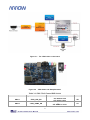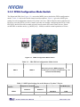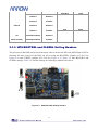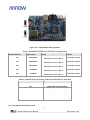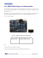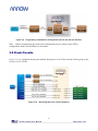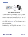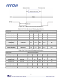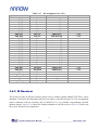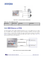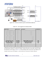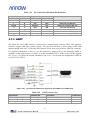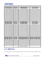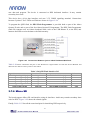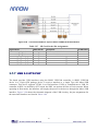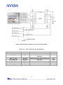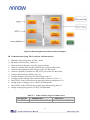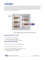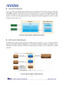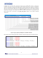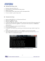
1
1 CONTENTS Chapter 1 SoCKit Development Kit ........................................................................... 4 1.1 Package Contents .................................................................................................................................. 4 1.2 SoCKit System CD ............................................................................................................................... 5 1.3 Getting Help ......................................................................................................................................... 5 Chapter 2 Introduction of the SoCKit Board ............................................................... 6 2.1 Layout and Components........................................................................................................................ 6 2.2 Block Diagram of the SoCKit Board ..................................................................................................... 9 Chapter 3 Using the SoCKit Board.......................................................................... 11 3.1 Board Setup Components .................................................................................................................... 11 3.1.1 JTAG Chain and Setup Switches ...................................................................................................... 11 3.1.2 FPGA Configuration Mode Switch ................................................................................................... 13 3.1.3 HPS BOOTSEL and CLKSEL Setting Headers ................................................................................ 14 3.1.4 HSMC VCCIO Voltage Level Setting Header ................................................................................... 16 3.2 Board Status Elements ........................................................................................................................ 17 3.3 Board Reset Elements ......................................................................................................................... 17 3.4 Programming the Quad-Serial Configuration Device ........................................................................... 19 3.5 Clock Circuits ..................................................................................................................................... 20 3.6 Interface on FPGA .............................................................................................................................. 21 3.6.1 User Push-buttons, Switches and LED on FPGA .............................................................................. 21 3.6.2 HSMC connector.............................................................................................................................. 24 3.6.3 Audio CODEC ................................................................................................................................. 27 3.6.4 VGA ......................................................................................................................................... 28 3.6.5 IR Receiver ...................................................................................................................................... 31 3.6.6 DDR3 Memory on FPGA................................................................................................................. 32 3.6.7 Temperature Sensor .......................................................................................................................... 35 1 3.7 Interface on Hard Processor System (HPS) .......................................................................................... 35 3.7.1 User Push-buttons, Switches and LED on HPS ................................................................................. 36 3.7.2 Gigabit Ethernet ............................................................................................................................... 36 3.7.3 UART ......................................................................................................................................... 38 3.7.4 DDR3 Memory on HPS.................................................................................................................... 39 3.7. QSPI Flash ......................................................................................................................................... 40 3.7.6 Micro SD ......................................................................................................................................... 41 3.7.7 USB 2.0 OTG PHY.......................................................................................................................... 42 3.7.8 G-Sensor ......................................................................................................................................... 43 3.7.9 128x64 Dots LCD ............................................................................................................................ 44 3.7.10 LTC Connector............................................................................................................................... 45 Chapter 4 SoCKit System Builder ........................................................................... 47 4.1 Introduction ........................................................................................................................................ 47 4.2 General Design Flow........................................................................................................................... 47 4.3 Using SoCKit System Builder ............................................................................................................. 48 Chapter 5 Examples For FPGA .............................................................................. 54 5.1 Audio Recording and Playing .............................................................................................................. 54 5.2 A Karaoke Machine............................................................................................................................. 57 5.3 DDR3 SDRAM Test............................................................................................................................ 60 5.4 DDR3 SDRAM Test by Nios II ........................................................................................................... 62 5.5 IR Receiver Demonstration ................................................................................................................. 64 5.6 Temperature Demonstration ................................................................................................................ 69 Chapter 6 Examples for HPS SoC .......................................................................... 72 6.1 Hello Program..................................................................................................................................... 72 6.2 Users LED, Switch and Button............................................................................................................ 74 6.3 I2C Interfaced G-sensor ...................................................................................................................... 82 6.4 SPI Interfaced Graphic LCD ............................................................................................................... 85 Chapter 7 Steps of Programming the Quad Serial Configuration Device.................... 89 2 Chapter 8 Appendix ............................................................................................... 96 8.1 Revision History ................................................................................................................................. 96 8.2 Copyright Statement............................................................................................................................ 96 3 Chapter 1 SoCKit Development Kit The SoCKit Development Kit presents a robust hardware design platform built around the Altera System-on-Chip (SoC) FPGA, which combines the latest dual-core Cortex-A9 embedded cores with industry-leading programmable logic for ultimate design flexibility. Users can now leverage the power of tremendous re-configurability paired with a high-performance, low-power processor system. Altera’s SoC integrates an ARM-based hard processor system (HPS) consisting of processor, peripherals and memory interfaces tied seamlessly with the FPGA fabric using a high-bandwidth interconnect backbone. The SoCKit development board includes hardware such as high-speed DDR3 memory, video and audio capabilities, Ethernet networking, and much more. In addition, an on-board HSMC connector with high-speed transceivers allows for an even greater array of hardware setups. By leveraging all of these capabilities, the SoCKit is the perfect solution for showcasing, evaluating, and prototyping the true potential of the Altera SoC. The SoCKit Development Kit contains all components needed to use the board in conjunction with a computer that runs the Microsoft Windows XP or later. 1.1 Package Contents Figure 1-1 shows a photograph of the SoCKit package. Figure 1-1 The SoCKit package contents 4 The SoCKit package includes: • • • • The SoCKit development board USB Cable for FPGA programming and control Ethernet Cable 12V DC power adapter 1.2 SoCKit System CD The SoCKit System CD containing the SoCKit documentation and supporting materials, including the User Manual, System Builder, reference designs and device datasheets. User can download this System CD form the link : http:/sockit_support.terasic.com. 1.3 Getting Help For discussion, support, and reference designs, please go to: RocketBoards.org Arrow SoCKit Evaluation Board Arrow SoCKIT Evaluation Board - How to Boot Linux Here are the addresses where you can get help if you encounter any problem: • Terasic Technologies Taiwan/ 9F, No.176, Sec.2, Gongdao 5th Rd, East Dist, Hsinchu City, Taiwan 300-70 Email: [email protected] Tel.: +886-3-5750-880 Web: http://sockit.terasic.com 5 Chapter 2 Introduction of the SoCKit Board This chapter presents the features and design characteristics of the board. 2.1 Layout and Components A photograph of the board is shown in Figure 2-1 and Figure 2-2. It depicts the layout of the board and indicates the location of the connectors and key components. HPS FPGA System Ethernet 10/100/1000 VGA USB 2.0 OTG 24-bit DAC Port Port JTAG USB Blaster II USB-UART Header Port Port VGA OUT DB-15 Connector Line In Mic In Line Out Bottom Side Components: *QSPI Flash 128MB *Micro SD Card Socket *FPGA Configuration Mode Switch USB-UART Controller JTAG Switch 12V DC Power Supply Connector Audio Codec Altera USB Blaster II Controller Chip FPGA DDR3 1GB Power ON/OFF Switch EPCQ 256Mb USB OTG Controller (ULPI) HSMC Connector TSE PHY LTC Connector Altera 28-nm Cyclone V FPGA with ARM Cortex-A9 HPS DDR3 1GB CLKSEL Jumper BOOTSEL Jumper 128x64 Dots LCD Temperature Sensor G-Sensor Clock Circuit for FPGA and HPS IR Receiver LCD Backlight Jumper HPS System Reset Keys HPS User Keys HPS User FPGA User FPGA User Keys Switches Switches HPS User FPGA User FPGA Reset Key LEDs LEDs Figure 2-1 Development Board (top view) 6 HSMC Voltage-Level Jumper Figure 2-2 Development Board (bottom view) The board has many features that allow users to implement a wide range of designed circuits, from simple circuits to various multimedia projects. The following hardware is provided on the board: FPGA Device • • • • • • • Cyclone V SoC 5CSXFC6D6F31 Device Dual-core ARM Cortex-A9 (HPS) 110K Programmable Logic Elements 5,140 Kbits embedded memory 6 Fractional PLLs 2 Hard Memory Controllers 3.125G Transceivers 7 Configuration and De bug • • Quad Serial Configuration device – EPCQ256 on FPGA On-Board USB Blaster II (micro USB type B connector) Memory Device • • • • 1GB (2x256MBx16) DDR3 SDRAM on FPGA 1GB (2x256MBx16) DDR3 SDRAM on HPS 128MB QSPI Flash on HPS Micro SD Card Socket on HPS Communication • • • USB 2.0 OTG (ULPI interface with micro USB type AB connector) USB to UART (micro USB type B connector) 10/100/1000 Ethernet Connectors • • One HSMC (8-channel Transceivers, Configurable I/O standards 1.5/1.8/2.5/3.3V) One LTC connector (One Serial Peripheral Interface (SPI) Master ,one I2C and one GPIO interface ) Display • • 24-bit VGA DAC 128x64 dots LCD Module with Backlight Audio • 24-bit CODEC, Line-in, line-out, and microphone-in jacks Switc hes, B uttons and LEDs • • • • 8 User Keys (FPGA x4 ; HPS x 4) 8 User Switches (FPGA x4 ; HPS x 4) 8 User LEDs (FPGA x4 ; HPS x 4) 2 HPS Reset Buttons (HPS_RSET_n and HPS_WARM_RST_n) 8 Se nsors • • G-Sensor on HPS Temperature Sensor on FPGA Power • 12V DC input 2.2 Block Diagram of the SoCKit Boar d Figure 2-3 gives the block diagram of the board. To provide maximum flexibility for the user, all connections are made through the Cyclone V SoC FPGA device. Thus, the user can configure the FPGA to implement any system design. 9 Figure 2-3 Board Block Diagram 10 Chapter 3 Using the SoCKit Board This chapter gives instructions for using the board and describes each of its peripherals. 3.1 Board Setup Components The SoCKit includes several jumpers, switches, etc. that control various system functions including JTAG chain, HSMC I/O voltage control, HPS boot source select, and others. This section will explain the settings and functions in detail. 3.1.1 JTAG Chain and Setup Switches The SoCKit allows users to access the FPGA, HPS debug, or other JTAG chain devices via the on-board USB Blaster II. Figure 3-1 shows the JTAG chain. Users can control whether the HPS or HSMC connector is included in the JTAG chain via SW4 (See Figure 3-2), where Table 3-1 lists the configuration details 11 Figure 3-1 The JTAG chain on the board Figure 3-2 JTAG Chain and Setup Switches Table 3-1 SW4 JTAG Control DIP Switch Board Reference Signal Name SW4.1 JTAG_HPS_EN SW4.2 JTAG_HSMC_EN Description On: Bypass HPS Off: HPS In-chain On: Bypass HSMC Off: HSMC In-chain 12 Default Off On 3.1.2 FPGA Configur ation Mode Switch The Dipswitch SW6 (See Figure 3-3) can set the MSEL pins to decide the FPGA configuration modes. Table 3-2 shows the switch controls and descriptions. Table 3-3 gives the MSEL pins setting for each configuration scheme of Cyclone V devices. FPGA default works in ASx4 mode. However, once the FPGA is in AS x4 mode, and after successfully configuring the FPGA via the EPCQ256, the SoCKit will be unable to boot Linux from the SD card or other devices. Please switch SW6 to another mode (e.g. MSEL[4:0] = 10000) to enable normal operations of Linux. Figure 3-3 Table 3-2 Board Reference SW6.1 SW6.2 SW6.3 SW6.4 SW6.5 SW6.6 FPGA Configuration Mode Switch SW6 FPGA Configuration Mode Switch Signal Name Description MSEL0 MSEL1 MSEL2 MSEL3 MSEL4 N/A Default Sets the Cyclone V MSEL[4:0] pins. Use these pins to set the configuration scheme and POR delay. N/A On Off On On Off N/A Table 3-3 MSEL pin Settings for each Scheme of Cyclone V Device Configuration Scheme FPPx8 Compression Feature Design Security POR Delay Feature Disabled Disabled Disabled Enabled 13 Fast Standard Fast Valid MSEL[4:0] 10100 11000 10101 Enabled Disabled Disabled Enabled Disabled Disabled Enabled Enabled PS Enabled/ Disabled Disabled AS(X1 and X4) Enabled/ Disabled Enabled FPPx16 Standard Fast 11001 10110 Standard Fast Standard 11010 00000 00100 Fast Standard Fast 00001 00101 00010 Standard Fast Standard 00110 10000 10001 Fast Standard 10010 10011 3.1.3 HPS BOOTSEL and CLKSEL Setting Headers The processor in the HPS can be boot from many sources such as the SD card, QSPI Flash or FPGA. Selecting the boot source for the HPS can be set using the BOOTSEL jumpers (J17~J19, See Figure 3-4) and CLKSEL jumpers (J15~J16, See Figure 3-5). Table 3-4 lists BOOTSEL and CLKSEL settings. Table 3-5 lists the settings for selecting a suitable boot source. Figure 3-4 HPS BOOTSEL Setting Headers 14 Figure 3-5 HPS CLKSEL Setting Headers Table 3-4 HPS BOOTSEL and CLKSEL Setting Headers Board Reference Signal Name J17 BOOTSEL0 J19 BOOTSEL1 J18 BOOTSEL2 J15 CLKSEL0 J16 CLKSEL1 Setting Short Pin 1 and 2: Short Pin 2 and 3: Short Pin 1 and 2: Short Pin 2 and 3: Short Pin 1 and 2: Short Pin 2 and 3: Short Pin 1 and 2: Short Pin 2 and 3: Short Pin 1 and 2: Short Pin 2 and 3: Default Logic 1 Logic 0 Logic 1 Logic 0 Logic 1 Logic 0 Logic 1 Logic 0 Logic 1 Logic 0 Short Pin 1 and 2 Short Pin 2 and 3 Short Pin 1 and 2 Short Pin 2 and 3 Short Pin 2 and 3 Table 3-5 BOOTSEL[2:0] Setting Values and Flash Device Selection BOOTSEL[2:0] Setting Value 000 001 010 011 100 101 110 111 Flash Device Reserved FPGA (HPS-to-FPGA bridge) 1.8 V NAND Flash memory (*1) 3.0 V NAND Flash memory(*1) 1.8 V SD/MMC Flash memory(*1) 3.0 V SD/MMC Flash memory 1.8 V SPI or quad SPI Flash memory(*1) 3.0 V SPI or quad SPI Flash memory (*1) : Not supported on SoCKit board 15 3.1.4 HSMC VCCIO Voltage Level Setting Header On the SoCKit, the I/O standards of the FPGA/HSMC pins can be adjusted via JP2 (See Figure 3-6). Adjustable standards allow even more flexibility and selection of daughter cards or interconnect devices. The HSMC connector’s default standard is 2.5V. Users must ensure that the voltage standards for both the main board and daughter card are the same, or damage/incompatibility may occur. Table 3-6 lists JP2 settings. Figure 3-6 HSMC VCCIO Voltage Level Setting Header Table 3-6 JP2 Header Setting for Different I/O Standard JP2 Jumper Setting Short Pin 1 and 2 Short Pin 3 and 4 Short Pin 5 and 6 Short Pin 7 and 8 I/O Voltage of HSMC Connector 1.5V 1.8V 2.5V (Default) 3.3V Note: 1. JP2 only allows for one jumper at one time. 2. If no jumper is attached on JP2, the voltage standard will default to 1.5V 16 3.2 Board Status Elements The board includes status LEDs. Please refer to Table 3-7 for the status of the LED indicator. Table 3-7 LED Indicators Board Reference LED Name Description D5 12-V Power Illuminates when 12-V power is active. TXD UART TXD Illuminates when data from FT232R to USB Host. RXD UART RXD Illuminates when data from USB Host to FT232R. D9 HSMC PSNTN D1 JTAG_RX D2 JTAG_TX D3 SC_RX D4 SC_TX Illuminates when connecting a daughter card on HSMC connector. Reserved 3.3 Board Reset Elements The board equips two HPS reset circuits and one FPGA Device Clear button (See Figure 3-7). Table 3-8 shows the buttons references and its descriptions. Figure 3-8 shows the reset tree on the board. 17 Figure 3-7 Board Reset Elements Table 3-8 Reset Elements Board Reference Signal Name KEY5 KEY6 KEY4 Description Cold reset to the HPS , Ethernet PHY, UART and USB OTG device . Active low input that will reset all HPS logics that can HPS_RESET_n be reset. Places the HPS in a default state sufficient for software to boot. Warm reset to the HPS block. Active low input affects the HPS_WARM_RST_n system reset domains which allows debugging to operate. This signal connects to the Cyclone V DEV_CLRn pin. When FPGA_RESET_n this pin is driven low, all the device registers are. 18 Figure 3-8 Reset Tree on the Development Board 3.4 Pr ogr amming the Quad-Serial Configur ation Device • • • The board contains a quad serial configuration device (EPCQ256) that stores configuration data for the Cyclone V SoC FPGA. This configuration data is automatically loaded from the quad serial configuration device chip into the FPGA when the board is powered up. To program the configuration device, users will need to use a Serial Flash Loader (SFL) function to program the quad serial configuration device via the JTAG interface. The FPGA-based SFL is a soft intellectual property (IP) core within the FPGA that bridges the JTAG and flash interfaces. The SFL mega-function is available from Quartus II software. Figure 3-9 shows the programming method when adopting a SFL solution Please refer to Chapter 6: Steps of Programming the Quad Serial Configuration Device for the basic programming instruction on the serial configuration device 19 Figure 3-9 Programming a Quad Serial Configuration Device with the SFL Solution Note: Before programming the quad serial configuration device, please set the FPGA configuration mode switch (SW6) to ASx4 mode. 3.5 Clock Cir cuits Figure 3-10 is a diagram showing the default frequencies of all of the external clocks going to the Cyclone V SoC FPGA. Figure 3-10 Block diagram of the clock distribution 20 3.6 Interface on FPGA This section describes the interfaces to the FPGA. Users can control or monitor the different interfaces with user logic on the FPGA. 3.6.1 User Push-buttons, Switches and LED on FPGA The board provides four push-button switches connected to FPGA as shown in Figure 3-11. Each of these switches is debounced using a Schmitt Trigger circuit, as indicated in Figure 3-12. The four outputs called KEY0, KEY1, KEY2, and KEY3 of the Schmitt Trigger devices are connected directly to the Cyclone V SoC FPGA. Each push-button switch provides a high logic level when it is not pressed, and provides a low logic level when depressed. Since the push-button switches are debounced, they are appropriate for using as clock or reset inputs in a circuit. Figure 3-11 Connections between the push-button and Cyclone V SoC FPGA Pushbutton depressed Pushbutton released Before Debouncing Schmitt Trigger Debounced Figure 3-12 Switch debouncing 21 There are four slide switches connected to FPGA on the board (See Figure 3-13). These switches are not debounced, and are assumed for use as level-sensitive data inputs to a circuit. Each switch is connected directly to a pin on the Cyclone V SoC FPGA. When the switch is in the DOWN position (closest to the edge of the board), it provides a low logic level to the FPGA, and when the switch is in the UP position it provides a high logic level. Figure 3-13 Connections between the slide switches and Cyclone V SoC FPGA There are also four user-controllable LEDs connected to FPGA on the board. Each LED is driven directly by a pin on the Cyclone V SoC FPGA; driving its associated pin to a high logic level turns the LED on, and driving the pin low turns it off. Figure 3-14 shows the connections between LEDs and Cyclone V SoC FPGA. Table 3-9, Table 3-10 and Table 3-11 list the pin assignments of these user interfaces. 22 Figure 3-14 Connections between the LEDs and Cyclone V SoC FPGA Table 3-9 Signal Name SW[0] SW[1] SW[2] SW[3] Pin Assignments for Slide Switches FPGA Pin No. PIN_W25 PIN_V25 PIN_AC28 PIN_AC29 Table 3-10 Signal Name KEY[0] KEY[1] KEY[2] KEY[3] Description Slide Switch[0] Slide Switch[1] Slide Switch[2] Slide Switch[3] FPGA Pin No. PIN_AE9 PIN_AE12 PIN_AD9 PIN_AD11 FPGA Pin No. PIN_AF10 PIN_AD10 PIN_AE11 PIN_AD7 2.5V 2.5V 2.5V 2.5V Pin Assignments for Push-buttons Table 3-11 Signal Name LED[0] LED[1] LED[2] LED[3] I/O Standard Description Push-button[0] Push-button[1] Push-button[2] Push-button[3] I/O Standard 3.3V 3.3V 3.3V 3.3V Pin Assignments for LEDs Description LED [0] LED [1] LED [2] LED [3] 23 I/O Standard 3.3V 3.3V 3.3V 3.3V 3.6.2 HSMC connector The board contains a High Speed Mezzanine Card (HSMC) interface to provide a mechanism for extending the peripheral-set of an FPGA host board by means of add-on daughter cards, which can address today’s high speed signaling requirements as well as low-speed device interface support. The HSMC interface support JTAG, clock outputs and inputs, high-speed serial I/O (transceivers), and single-ended or differential signaling. Signals on the HSMC port are shown in Figure 3-15. Table 3-12 shows the maximum power consumption of the daughter card that connects to HSMC port. Figure 3-15 Table 3-12 Supplied Voltage Power Supply of the HSMC Max. Current Limit 12V 1A 3.3V 1.5A Table 3-13 Signal Name HSMC_CLK_IN0 HSMC_CLKIN_n1 HSMC Signal Bank Diagram Pin Assignments for HSMC connector FPGA Pin No. PIN_J14 PIN_AB27 Description Dedicated clock input LVDS RX or CMOS I/O or differential clock input 24 I/O Standard Depend on JP2 Depend on JP2 HSMC_CLKIN_n2 PIN_G15 HSMC_CLKIN_p1 PIN_AA26 HSMC_CLKIN_p2 PIN_H15 HSMC_CLK_OUT0 HSMC_CLKOUT_n1 PIN_AD29 PIN_E6 HSMC_CLKOUT_n2 PIN_A10 HSMC_CLKOUT_p1 PIN_E7 HSMC_CLKOUT_p2 PIN_A11 HSMC_D[0] HSMC_D[1] HSMC_D[2] HSMC_D[3] HSMC_SCL HSMC_SDA HSMC_GXB_RX_p[0] HSMC_GXB_RX_p[1] HSMC_GXB_RX_p[2] HSMC_GXB_RX_p[3] HSMC_GXB_RX_p[4] HSMC_GXB_RX_p[5] HSMC_GXB_RX_p[6] HSMC_GXB_RX_p[7] HSMC_GXB_TX_p[0] HSMC_GXB_TX_p[1] HSMC_GXB_TX_p[2] HSMC_GXB_TX_p[3] HSMC_GXB_TX_p[4] HSMC_GXB_TX_p[5] HSMC_GXB_TX_p[6] HSMC_GXB_TX_p[7] HSMC_GXB_RX_n[0] HSMC_GXB_RX_n[1] HSMC_GXB_RX_n[2] HSMC_GXB_RX_n[3] HSMC_GXB_RX_n[4] HSMC_GXB_RX_n[5] HSMC_GXB_RX_n[6] HSMC_GXB_RX_n[7] HSMC_GXB_TX_n[0] PIN_C10 PIN_H13 PIN_C9 PIN_H12 PIN_AA28 PIN_AE29 PIN_AE2 PIN_AC2 PIN_AA2 PIN_W2 PIN_U2 PIN_R2 PIN_N2 PIN_J2 PIN_AD4 PIN_AB4 PIN_Y4 PIN_V4 PIN_T4 PIN_P4 PIN_M4 PIN_H4 PIN_AE1 PIN_AC1 PIN_AA1 PIN_W1 PIN_U1 PIN_R1 PIN_N1 PIN_J1 PIN_AD3 LVDS RX or CMOS I/O or differential clock input LVDS RX or CMOS I/O or differential clock input LVDS RX or CMOS I/O or differential clock input Dedicated clock output LVDS TX or CMOS I/O or differential clock input/output LVDS TX or CMOS I/O or differential clock input/output LVDS TX or CMOS I/O or differential clock input/output LVDS TX or CMOS I/O or differential clock input/output LVDS TX or CMOS I/O LVDS RX or CMOS I/O LVDS TX or CMOS I/O LVDS RX or CMOS I/O Management serial data Management serial clock Transceiver RX bit 0 Transceiver RX bit 1 Transceiver RX bit 2 Transceiver RX bit 3 Transceiver RX bit 4 Transceiver RX bit 5 Transceiver RX bit 6 Transceiver RX bit 7 Transceiver TX bit 0 Transceiver TX bit 1 Transceiver TX bit 2 Transceiver TX bit 3 Transceiver TX bit 4 Transceiver TX bit 5 Transceiver TX bit 6 Transceiver TX bit 7 Transceiver RX bit 0n Transceiver RX bit 1n Transceiver RX bit 2n Transceiver RX bit 3n Transceiver RX bit 4n Transceiver RX bit 5n Transceiver RX bit 6n Transceiver RX bit 7n Transceiver TX bit 0n 25 Depend on JP2 Depend on JP2 Depend on JP2 Depend on JP2 Depend on JP2 Depend on JP2 Depend on JP2 Depend on JP2 Depend on JP2 Depend on JP2 Depend on JP2 Depend on JP2 Depend on JP2 Depend on JP2 1.5-V PCML 1.5-V PCML 1.5-V PCML 1.5-V PCML 1.5-V PCML 1.5-V PCML 1.5-V PCML 1.5-V PCML 1.5-V PCML 1.5-V PCML 1.5-V PCML 1.5-V PCML 1.5-V PCML 1.5-V PCML 1.5-V PCML 1.5-V PCML 1.5-V PCML 1.5-V PCML 1.5-V PCML 1.5-V PCML 1.5-V PCML 1.5-V PCML 1.5-V PCML 1.5-V PCML 1.5-V PCML HSMC_GXB_TX_n[1] HSMC_GXB_TX_n[2] HSMC_GXB_TX_n[3] HSMC_GXB_TX_n[4] HSMC_GXB_TX_n[5] HSMC_GXB_TX_n[6] HSMC_GXB_TX_n[7] HSMC_RX _n[0] HSMC_RX _n[1] HSMC_RX _n[2] HSMC_RX _n[3] HSMC_RX _n[4] HSMC_RX _n[5] HSMC_RX _n[6] HSMC_RX _n[7] HSMC_RX _n[8] HSMC_RX _n[9] HSMC_RX _n[10] HSMC_RX _n[11] HSMC_RX _n[12] HSMC_RX _n[13] HSMC_RX _n[14] HSMC_RX _n[15] HSMC_RX _n[16] HSMC_RX _p[0] HSMC_RX _p[1] HSMC_RX _p[2] HSMC_RX _p[3] HSMC_RX _p[4] HSMC_RX _p[5] HSMC_RX _p[6] HSMC_RX _p[7] HSMC_RX _p[8] HSMC_RX _p[9] HSMC_RX _p[10] HSMC_RX _p[11] HSMC_RX _p[12] HSMC_RX _p[13] HSMC_RX _p[14] HSMC_RX _p[15] HSMC_RX _p[16] HSMC_TX _n[0] HSMC_TX _n[1] HSMC_TX _n[2] HSMC_TX _n[3] HSMC_TX _n[4] PIN_AB3 PIN_Y3 PIN_V3 PIN_T3 PIN_P3 PIN_M3 PIN_H3 PIN_G11 PIN_J12 PIN_F10 PIN_J9 PIN_K8 PIN_H7 PIN_G8 PIN_F8 PIN_E11 PIN_B5 PIN_D9 PIN_D12 PIN_D10 PIN_B12 PIN_E13 PIN_G13 PIN_F14 PIN_G12 PIN_K12 PIN_G10 PIN_J10 PIN_K7 PIN_J7 PIN_H8 PIN_F9 PIN_F11 PIN_B6 PIN_E9 PIN_E12 PIN_D11 PIN_C13 PIN_F13 PIN_H14 PIN_F15 PIN_A8 PIN_D7 PIN_F6 PIN_C5 PIN_C4 Transceiver TX bit 1n Transceiver TX bit 2n Transceiver TX bit 3n Transceiver TX bit 4n Transceiver TX bit 5n Transceiver TX bit 6n Transceiver TX bit 7n LVDS RX bit 0n or CMOS I/O LVDS RX bit 1n or CMOS I/O LVDS RX bit 2n or CMOS I/O LVDS RX bit 3n or CMOS I/O LVDS RX bit 4n or CMOS I/O LVDS RX bit 5n or CMOS I/O LVDS RX bit 6n or CMOS I/O LVDS RX bit 7n or CMOS I/O LVDS RX bit 8n or CMOS I/O LVDS RX bit 9n or CMOS I/O LVDS RX bit 10n or CMOS I/O LVDS RX bit 11n or CMOS I/O LVDS RX bit 12n or CMOS I/O LVDS RX bit 13n or CMOS I/O LVDS RX bit 14n or CMOS I/O LVDS RX bit 15n or CMOS I/O LVDS RX bit 16n or CMOS I/O LVDS RX bit 0 or CMOS I/O LVDS RX bit 1 or CMOS I/O LVDS RX bit 2 or CMOS I/O LVDS RX bit 3 or CMOS I/O LVDS RX bit 4 or CMOS I/O LVDS RX bit 5 or CMOS I/O LVDS RX bit 6 or CMOS I/O LVDS RX bit 7 or CMOS I/O LVDS RX bit 8 or CMOS I/O LVDS RX bit 9 or CMOS I/O LVDS RX bit 10 or CMOS I/O LVDS RX bit 11 or CMOS I/O LVDS RX bit 12 or CMOS I/O LVDS RX bit 13 or CMOS I/O LVDS RX bit 14 or CMOS I/O LVDS RX bit 15 or CMOS I/O LVDS RX bit 16 or CMOS I/O LVDS TX bit 0n or CMOS I/O LVDS TX bit 1n or CMOS I/O LVDS TX bit 2n or CMOS I/O LVDS TX bit 3n or CMOS I/O LVDS TX bit 4n or CMOS I/O 26 1.5-V PCML 1.5-V PCML 1.5-V PCML 1.5-V PCML 1.5-V PCML 1.5-V PCML 1.5-V PCML Depend on JP2 Depend on JP2 Depend on JP2 Depend on JP2 Depend on JP2 Depend on JP2 Depend on JP2 Depend on JP2 Depend on JP2 Depend on JP2 Depend on JP2 Depend on JP2 Depend on JP2 Depend on JP2 Depend on JP2 Depend on JP2 Depend on JP2 Depend on JP2 Depend on JP2 Depend on JP2 Depend on JP2 Depend on JP2 Depend on JP2 Depend on JP2 Depend on JP2 Depend on JP2 Depend on JP2 Depend on JP2 Depend on JP2 Depend on JP2 Depend on JP2 Depend on JP2 Depend on JP2 Depend on JP2 Depend on JP2 Depend on JP2 Depend on JP2 Depend on JP2 Depend on JP2 HSMC_TX _n[5] HSMC_TX _n[6] HSMC_TX _n[7] HSMC_TX _n[8] HSMC_TX _n[9] HSMC_TX _n[10] HSMC_TX _n[11] HSMC_TX _n[12] HSMC_TX _n[13] HSMC_TX _n[14] HSMC_TX _n[15] HSMC_TX _n[16] HSMC_TX _p[0] HSMC_TX _p[1] HSMC_TX _p[2] HSMC_TX _p[3] HSMC_TX _p[4] HSMC_TX _p[5] HSMC_TX _p[6] HSMC_TX _p[7] HSMC_TX _p[8] HSMC_TX _p[9] HSMC_TX _p[10] HSMC_TX _p[11] HSMC_TX _p[12] HSMC_TX _p[13] HSMC_TX _p[14] HSMC_TX _p[15] HSMC_TX _p[16] PIN_E2 PIN_D4 PIN_B3 PIN_D1 PIN_C2 PIN_B1 PIN_A3 PIN_A5 PIN_B7 PIN_B8 PIN_B11 PIN_A13 PIN_A9 PIN_E8 PIN_G7 PIN_D6 PIN_D5 PIN_E3 PIN_E4 PIN_C3 PIN_E1 PIN_D2 PIN_B2 PIN_A4 PIN_A6 PIN_C7 PIN_C8 PIN_C12 PIN_B13 LVDS TX bit 5n or CMOS I/O LVDS TX bit 6n or CMOS I/O LVDS TX bit 7n or CMOS I/O LVDS TX bit 8n or CMOS I/O LVDS TX bit 9n or CMOS I/O LVDS TX bit 10n or CMOS I/O LVDS TX bit 11n or CMOS I/O LVDS TX bit 12n or CMOS I/O LVDS TX bit 13n or CMOS I/O LVDS TX bit 14n or CMOS I/O LVDS TX bit 15n or CMOS I/O LVDS TX bit 16n or CMOS I/O LVDS TX bit 0 or CMOS I/O LVDS TX bit 1 or CMOS I/O LVDS TX bit 2 or CMOS I/O LVDS TX bit 3 or CMOS I/O LVDS TX bit 4 or CMOS I/O LVDS TX bit 5 or CMOS I/O LVDS TX bit 6 or CMOS I/O LVDS TX bit 7 or CMOS I/O LVDS TX bit 8 or CMOS I/O LVDS TX bit 9 or CMOS I/O LVDS TX bit 10 or CMOS I/O LVDS TX bit 11 or CMOS I/O LVDS TX bit 12 or CMOS I/O LVDS TX bit 13 or CMOS I/O LVDS TX bit 14 or CMOS I/O LVDS TX bit 15 or CMOS I/O LVDS TX bit 16 or CMOS I/O Depend on JP2 Depend on JP2 Depend on JP2 Depend on JP2 Depend on JP2 Depend on JP2 Depend on JP2 Depend on JP2 Depend on JP2 Depend on JP2 Depend on JP2 Depend on JP2 Depend on JP2 Depend on JP2 Depend on JP2 Depend on JP2 Depend on JP2 Depend on JP2 Depend on JP2 Depend on JP2 Depend on JP2 Depend on JP2 Depend on JP2 Depend on JP2 Depend on JP2 Depend on JP2 Depend on JP2 Depend on JP2 Depend on JP2 3.6.3 Audio CODEC The board provides high-quality 24-bit audio via the Analog Devices SSM2603 audio CODEC (Encoder/Decoder). This chip supports microphone-in, line-in, and line-out ports, with a sample rate adjustable from 8 kHz to 96 kHz. The SSM2603 is controlled via a serial I2C bus interface, which is connected to pins on the Cyclone V SoC FPGA. A schematic diagram of the audio circuitry is shown in Figure 3-16. Detailed information for using the SSM2603 codec is available in its datasheet, which can be found on the manufacturer’s website, or in the Datasheets\Audio CODEC folder on the SoCKit System CD 27 Figure 3-16 Connections between FPGA and Audio CODEC Table 3-14 Signal Name AUD_ADCLRCK AUD_ADCDAT AUD_DACLRCK AUD_DACDAT AUD_XCK AUD_BCLK AUD_I2C_SCLK AUD_I2C_SDAT AUD_MUTE FPGA Pin No. PIN_AG30 PIN_AC27 PIN_AH4 PIN_AG3 PIN_AC9 PIN_AE7 PIN_AH30 PIN_AF30 PIN_AD26 Pin Assignments for Audio CODEC Description Audio CODEC ADC LR Clock Audio CODEC ADC Data Audio CODEC DAC LR Clock Audio CODEC DAC Data Audio CODEC Chip Clock Audio CODEC Bit-Stream Clock I2C Clock I2C Data DAC Output Mute, Active Low I/O Standard 3.3V 3.3V 3.3V 3.3V 3.3V 3.3V 3.3V 3.3V 3.3V 3.6.4 VGA The board includes a 15-pin D-SUB connector for VGA output. The VGA synchronization signals are provided directly from the Cyclone V SoC FPGA, and the Analog Devices ADV7123 triple 10-bit high-speed video DAC (only the higher 8-bits are used) is used to produce the analog data signals (red, green, and blue). It could support the SXGA standard (1280*1024) with a bandwidth of 100MHz. Figure 3-17 gives the associated schematic. 28 Figure 3-17 VGA Connections between FPGA and VGA The timing specification for VGA synchronization and RGB (red, green, blue) data can be found on various educational website (for example, search for “VGA signal timing”). Figure 3-18 illustrates the basic timing requirements for each row (horizontal) that is displayed on a VGA monitor. An active-low pulse of specific duration (time (a) in the figure) is applied to the horizontal synchronization (hsync) input of the monitor, which signifies the end of one row of data and the start of the next. The data (RGB) output to the monitor must be off (driven to 0 V) for a time period called the back porch (b) after the hsync pulse occurs, which is followed by the display interval (c). During the data display interval the RGB data drives each pixel in turn across the row being displayed. Finally, there is a time period called the front porch (d) where the RGB signals must again be off before the next hsync pulse can occur. The timing of the vertical synchronization (vsync) is the similar as shown in Figure 3-18, except that a vsync pulse signifies the end of one frame and the start of the next, and the data refers to the set of rows in the frame (horizontal timing). Table 3-15 and Table 3-16 show different resolutions and durations of time periods a, b, c, and d for both horizontal and vertical timing. Detailed information for using the ADV7123 video DAC is available in its datasheet, which can be found on the manufacturer’s website, or in the Datasheets\VIDEO DAC folder on the SoCKit System CD. The pin assignments between the Cyclone V SoC FPGA and the ADV7123 are listed in Table 3-17 29 Figure 3-18 VGA horizontal timing specification Table 3-15 VGA Horizontal Timing Specification VGA mode Configuration VGA(60Hz) Horizontal Timing Spec Resolution(HxV) 640x480 a(us) 3.8 b(us) 1.9 c(us) 25.4 d(us) 0.6 Pixel clock(MHz) 25 VGA(85Hz) 640x480 1.6 2.2 17.8 1.6 36 SVGA(60Hz) 800x600 3.2 2.2 20 1 40 SVGA(75Hz) 800x600 1.6 3.2 16.2 0.3 49 SVGA(85Hz) 800x600 1.1 2.7 14.2 0.6 56 XGA(60Hz) 1024x768 2.1 2.5 15.8 0.4 65 XGA(70Hz) 1024x768 1.8 1.9 13.7 0.3 75 XGA(85Hz) 1024x768 1.0 2.2 10.8 0.5 95 1280x1024(60Hz) 1280x1024 1.0 2.3 11.9 0.4 108 d(lines) 10 1 1 1 1 3 3 1 1 Pixel clock(MHz) 25 36 40 49 56 65 75 95 108 Table 3-16 VGA Vertical Timing Specification VGA mode Configuration VGA(60Hz) VGA(85Hz) SVGA(60Hz) SVGA(75Hz) SVGA(85Hz) XGA(60Hz) XGA(70Hz) XGA(85Hz) 1280x1024(60Hz) Vertical Timing Spec Resolution(HxV) 640x480 640x480 800x600 800x600 800x600 1024x768 1024x768 1024x768 1280x1024 a(lines) 2 3 4 3 3 6 6 3 3 30 b(lines) 33 25 23 21 27 29 29 36 38 c(lines) 480 480 600 600 600 768 768 768 1024 Table 3-17 Signal Name VGA_R[0] VGA_R[1] VGA_R[2] VGA_R[3] VGA_R[4] VGA_R[5] VGA_R[6] VGA_R[7] VGA_G[0] VGA_G[1] VGA_G[2] VGA_G[3] VGA_G[4] VGA_G[5] VGA_G[6] VGA_G[7] VGA_B[0] VGA_B[1] VGA_B[2] VGA_B[3] VGA_B[4] VGA_B[5] VGA_B[6] VGA_B[7] VGA_CLK VGA_BLANK_n VGA_HS VGA_VS VGA_SYNC_n FPGA Pin No. PIN_AG5 PIN_AA12 PIN_AB12 PIN_AF6 PIN_AG6 PIN_AJ2 PIN_AH5 PIN_AJ1 PIN_Y21 PIN_AA25 PIN_AB26 PIN_AB22 PIN_AB23 PIN_AA24 PIN_AB25 PIN_AE27 PIN_AE28 PIN_Y23 PIN_Y24 PIN_AG28 PIN_AF28 PIN_V23 PIN_W24 PIN_AF29 PIN_W20 PIN_AH3 PIN_AD12 PIN_AC12 PIN_AG2 Pin Assignments for VGA Description VGA Red[0] VGA Red[1] VGA Red[2] VGA Red[3] VGA Red[4] VGA Red[5] VGA Red[6] VGA Red[7] VGA Green[0] VGA Green[1] VGA Green[2] VGA Green[3] VGA Green[4] VGA Green[5] VGA Green[6] VGA Green[7] VGA Blue[0] VGA Blue[1] VGA Blue[2] VGA Blue[3] VGA Blue[4] VGA Blue[5] VGA Blue[6] VGA Blue[7] VGA Clock VGA BLANK VGA H_SYNC VGA V_SYNC VGA SYNC I/O Standard 3.3V 3.3V 3.3V 3.3V 3.3V 3.3V 3.3V 3.3V 3.3V 3.3V 3.3V 3.3V 3.3V 3.3V 3.3V 3.3V 3.3V 3.3V 3.3V 3.3V 3.3V 3.3V 3.3V 3.3V 3.3V 3.3V 3.3V 3.3V 3.3V 3.6.5 IR Receiver The board provides an infrared remote-control receiver module (model: IRM-V5XX/TR1), whose datasheet is offered in the Datasheets\IR_Receiver folder on SoCKit System CD. The accompanied remote controller with an encoding chip of uPD6121G is very suitable of generating expected infrared signals. Figure 3-19 shows the related schematic of the IR receiver. Table 3-18 shows the IR receiver interface pin assignments. 31 Figure 3-19 Table 3-18 Connection between FPGA and IR Pin Assignments for IR Signal Name IRDA_RXD FPGA Pin No. PIN_ AH2 Description IR Receiver I/O Standard 3.3V 3.6.6 DDR3 Memory on FPGA The board supports 1GB of DDR3 SDRAM comprising of two x16 bit DDR3 devices on FPGA side. The DDR3 devices shipped with this board are running at 400MHz if the hard external memory interface is enabled, and at 300MHz if the hard external memory interface if not enabled. Figure 3-20 shows the connections between the DDR3 and Cyclone V SoC FPGA. Table 3-19 shows the DDR3 interface pin assignments. Figure 3-20 Connections between FPGA and DDR3 32 Table 3-19 Signal Name DDR3_A[0] DDR3_A[1] DDR3_A[2] DDR3_A[3] DDR3_A[4] DDR3_A[5] DDR3_A[6] DDR3_A[7] DDR3_A[8] DDR3_A[9] DDR3_A[10] DDR3_A[11] DDR3_A[12] DDR3_A[13] DDR3_A[14] DDR3_BA[0] DDR3_BA[1] DDR3_BA[2] DDR3_CAS_n DDR3_CKE FPGA Pin No. PIN_AJ14 PIN_AK14 PIN_AH12 PIN_AJ12 PIN_AG15 PIN_AH15 PIN_AK12 PIN_AK13 PIN_AH13 PIN_AH14 PIN_AJ9 PIN_AK9 PIN_AK7 PIN_AK8 PIN_AG12 PIN_AH10 PIN_AJ11 PIN_AK11 PIN_AH7 PIN_AJ21 DDR3_CK_n PIN_AA15 DDR3_CK_p PIN_AA14 DDR3_CS_n DDR3_DM[0] DDR3_DM[1] DDR3_DM[2] DDR3_DM[3] DDR3_DQ[0] DDR3_DQ[1] DDR3_DQ[2] DDR3_DQ[3] DDR3_DQ[4] DDR3_DQ[5] DDR3_DQ[6] DDR3_DQ[7] DDR3_DQ[8] DDR3_DQ[9] DDR3_DQ[10] DDR3_DQ[11] DDR3_DQ[12] DDR3_DQ[13] PIN_AB15 PIN_AH17 PIN_AG23 PIN_AK23 PIN_AJ27 PIN_AF18 PIN_AE17 PIN_AG16 PIN_AF16 PIN_AH20 PIN_AG21 PIN_AJ16 PIN_AH18 PIN_AK18 PIN_AJ17 PIN_AG18 PIN_AK19 PIN_AG20 PIN_AF19 Pin Assignments for DDR3 Description I/O Standard DDR3 Address[0] SSTL-15 Class I DDR3 Address[1] SSTL-15 Class I DDR3 Address[2] SSTL-15 Class I DDR3 Address[3] SSTL-15 Class I DDR3 Address[4] SSTL-15 Class I DDR3 Address[5] SSTL-15 Class I DDR3 Address[6] SSTL-15 Class I DDR3 Address[7] SSTL-15 Class I DDR3 Address[8] SSTL-15 Class I DDR3 Address[9] SSTL-15 Class I DDR3 Address[10] SSTL-15 Class I DDR3 Address[11] SSTL-15 Class I DDR3 Address[12] SSTL-15 Class I DDR3 Address[13] SSTL-15 Class I DDR3 Address[14] SSTL-15 Class I DDR3 Bank Address[0] SSTL-15 Class I DDR3 Bank Address[1] SSTL-15 Class I DDR3 Bank Address[2] SSTL-15 Class I DDR3 Column Address Strobe SSTL-15 Class I Clock Enable pin for DDR3 SSTL-15 Class I DIFFERENTIAL 1.5-V Clock for DDR3 SSTL CLASS I Differential 1.5-V SSTL Clock p for DDR3 Class I DDR3 Chip Select SSTL-15 Class I DDR3 Data Mask[0] SSTL-15 Class I DDR3 Data Mask[1] SSTL-15 Class I DDR3 Data Mask[2] SSTL-15 Class I DDR3 Data Mask[3] SSTL-15 Class I DDR3 Data[0] SSTL-15 Class I DDR3 Data[1] SSTL-15 Class I DDR3 Data[2] SSTL-15 Class I DDR3 Data[3] SSTL-15 Class I DDR3 Data[4] SSTL-15 Class I DDR3 Data[5] SSTL-15 Class I DDR3 Data[6] SSTL-15 Class I DDR3 Data[7] SSTL-15 Class I DDR3 Data[8] SSTL-15 Class I DDR3 Data[9] SSTL-15 Class I DDR3 Data[10] SSTL-15 Class I DDR3 Data[11] SSTL-15 Class I DDR3 Data[12] SSTL-15 Class I DDR3 Data[13] SSTL-15 Class I 33 DDR3_DQ[14] DDR3_DQ[15] DDR3_DQ[16] DDR3_DQ[17] DDR3_DQ[18] DDR3_DQ[19] DDR3_DQ[20] PIN_AJ20 PIN_AH24 PIN_AE19 PIN_AE18 PIN_AG22 PIN_AK22 PIN_AF21 DDR3 Data[14] DDR3 Data[15] DDR3 Data[16] DDR3 Data[17] DDR3 Data[18] DDR3 Data[19] DDR3 Data[20] DDR3_DQ[21] PIN_AF20 DDR3 Data[21] DDR3_DQ[22] DDR3_DQ[23] DDR3_DQ[24] DDR3_DQ[25] DDR3_DQ[26] DDR3_DQ[27] DDR3_DQ[28] DDR3_DQ[29] DDR3_DQ[30] DDR3_DQ[31] PIN_AH23 PIN_AK24 PIN_AF24 PIN_AF23 PIN_AJ24 PIN_AK26 PIN_AE23 PIN_AE22 PIN_AG25 PIN_AK27 DDR3 DDR3 DDR3 DDR3 DDR3 DDR3 DDR3 DDR3 DDR3 DDR3 DDR3_DQS_n[0] PIN_W16 DDR3 Data Strobe n[0] DDR3_DQS_n[1] PIN_W17 DDR3 Data Strobe n[1] DDR3_DQS_n[2] PIN_AA18 DDR3 Data Strobe n[2] DDR3_DQS_n[3] PIN_AD19 DDR3 Data Strobe n[3] DDR3_DQS_p[0] PIN_V16 DDR3 Data Strobe p[0] DDR3_DQS_p[1] PIN_V17 DDR3 Data Strobe p[1] DDR3_DQS_p[2] PIN_Y17 DDR3 Data Strobe p[2] DDR3_DQS_p[3] PIN_AC20 DDR3 Data Strobe p[3] DDR3_ODT DDR3_RAS_n DDR3_RESET_n DDR3_WE_n PIN_AE16 PIN_AH8 PIN_AK21 PIN_AJ6 DDR3_RZQ PIN_AG17 DDR3 On-die Termination DDR3 Row Address Strobe DDR3 Reset DDR3 Write Enable External reference ball for output drive calibration 34 Data[22] Data[23] Data[24] Data[25] Data[26] Data[27] Data[28] Data[29] Data[30] Data[31] SSTL-15 Class I SSTL-15 Class I SSTL-15 Class I SSTL-15 Class I SSTL-15 Class I SSTL-15 Class I SSTL-15 Class I SSTL-15 Class I SSTL-15 Class I SSTL-15 Class I SSTL-15 Class I SSTL-15 Class I SSTL-15 Class I SSTL-15 Class I SSTL-15 Class I SSTL-15 Class I SSTL-15 Class I SSTL-15 Class I Differential 1.5-V SSTL Class I Differential 1.5-V SSTL Class I Differential 1.5-V SSTL Class I Differential 1.5-V SSTL Class I Differential 1.5-V SSTL Class I Differential 1.5-V SSTL Class I Differential 1.5-V SSTL Class I Differential 1.5-V SSTL Class I SSTL-15 Class I SSTL-15 Class I SSTL-15 Class I SSTL-15 Class I 1.5V 3.6.7 Temperature Sensor The board contains a temperature sensor (Analog Devices ADT7301) to monitor the ambient temperature. It is a band gap temperature sensor with a 13-bit ADC to monitor and digitize the temperature reading to a resolution of 0.03125°C. The interface between sensor and FPGA is SPI serial interface. Detailed information for using the sensor is available in its datasheet, which can be found on the manufacturer’s website, or in the Datasheets\TEMP_Sensor folder on the SoCKit System CD. Figure 3-21 shows the connections between temperature sensor and Cyclone V SoC FPGA. Table 3-20 gives the all the pin assignments of the sensor. Figure 3-21 Connections between FPGA and Temperature Sensor Table 3-20 Signal Name TEMP_CS_n TEMP_DIN TEMP_DOUT TEMP_SCLK Pin Assignments for Temperature Sensor FPGA Pin No. PIN_AF8 PIN_AG7 PIN_AG1 PIN_AF9 Description Temp Sensor Chip Select Input Temp Sensor Serial Data Input Temp Sensor Serial Data Output Temp Sensor Serial Clock Input I/O Standard 3.3V 3.3V 3.3V 3.3V 3.7 Interface on Hard Processor System (HPS) This section introduces the interfaces connected to the HPS section of the FPGA. Users can access these interfaces via the HPS processor. 35 3.7.1 User Push-buttons, Switches and LED on HPS Like the FPGA, the HPS also features its own set of switches, buttons, LEDs, and other user interfaces. Users can control these interfaces for observing HPS status and debugging. Table 3-21 gives the all the pin assignments of all the user interfaces. Table 3-21 Signal Name HPS_KEY[0] HPS_KEY[1] HPS_KEY[2] HPS_KEY[3] HPS_SW[0] HPS_SW[1] HPS_SW[2] HPS_SW[3] HPS_LED[0] HPS_LED[1] HPS_LED[2] HPS_LED[3] Pin Assignments for LEDs, Switches and Buttons HPS GPIO GPI8 GPI9 GPI10 GPI11 GPI7 GPI6 GPI5 GPI4 GPIO54 GPIO55 GPIO56 GPIO57 Register/bit GPIO2[21] GPIO2[22] GPIO2[23] GPIO2[24] GPIO2[20] GPIO2[19] GPIO2[18] GPIO2[17] GPIO1[25] GPIO1[26] GPIO1[27] GPIO1[28] Function Input only Input only Input only Input only Input only Input only Input only Input only I/O I/O I/O I/O 3.7.2 Gigabit Ether net The board provides Ethernet support via an external Micrel KSZ9021RN PHY chip and HPS Ethernet MAC function. The KSZ9021RN chip with integrated 10/100/1000 Mbps Gigabit Ethernet transceiver support RGMII MAC interfaces. Figure 3-22 shows the connection setup between the Gigabit Ethernet PHY and Cyclone V SoC FPGA. The associated pin assignments are listed in Table 3-22. For detailed information on how to use the KSZ9021RN refers to its datasheet and application notes, which are available on the manufacturer’s website. 36 U13 HPS_ENET_TX_DATA[3..0] HPS_ENET_GTX_CLK HPS_ENET_TX_EN HPS_ENET_RX_DATA[3..0] HPS_ENET_RX_CLK HPS_ENET_RX_DV HPS_ENET_MDC HPS_ENET_MDIO HPS_ENET_INT_N HPS_ENET_RESET_N J11 TXD[3..0] GTX_CLK TX_EN RXD[3..0] RX_CLK RX_DV MDC MDIO TXRXP TXRXM LED1 LED2 MDI_HPS_N MDI_HPS_P LED2_DUAL_1 LED2-1 LED2_DUAL_2 LED2-2 INT_N RESET_N KSZ9021RN RJ45_1368589_5 Connections between Cyclone V SoC FPGA and Ethernet Table 3-22 Signal Name HPS_ENET_TX_EN HPS_ENET_TX_DATA[0] HPS_ENET_TX_DATA[1] HPS_ENET_TX_DATA[2] HPS_ENET_TX_DATA[3] HPS_ENET_RX_DV HPS_ENET_RX_DATA[0] HPS_ENET_RX_DATA[1] HPS_ENET_RX_DATA[2] HPS_ENET_RX_DATA[3] HPS_ENET_RX_CLK HPS_ENET_RESET_n HPS_ENET_MDIO HPS_ENET_MDC HPS_ENET_INT_n HPS_ENET_GTX_CLK TRD- X1 OSC_25 Figure 3-22 TRD+ Pin Assignments for Ethernet PHY FPGA Pin No. PIN_A20 PIN_F20 PIN_J19 PIN_F21 PIN_F19 PIN_K17 PIN_A21 PIN_B20 PIN_B18 PIN_D21 PIN_G20 PIN_E18 PIN_E21 PIN_B21 PIN_C19 PIN_H19 Description GMII and MII transmit enable MII transmit data[0] MII transmit data[1] MII transmit data[2] MII transmit data[3] GMII and MII receive data valid GMII and MII receive data[0] GMII and MII receive data[1] GMII and MII receive data[2] GMII and MII receive data[3] GMII and MII receive clock Hardware Reset Signal Management Data Management Data Clock Reference Interrupt Open Drain Output GMII Transmit Clock I/O Standard 3.3V 3.3V 3.3V 3.3V 3.3V 3.3V 3.3V 3.3V 3.3V 3.3V 3.3V 3.3V 3.3V 3.3V 3.3V 3.3V Additionally, the Ethernet PHY (KSZ9021RNI) LED status has been set to tri-color dual LED mode. The LED control signals are connected to LEDs (orange and green) on the RJ45 connector. States and definitions can be found in Table 3-23, which can display the current status of the Ethernet. For example once the green LED lights on , the board has been connected to Giga bit Ethernet. 37 Table 3-23 Tri-Color Dual LED Mode-Pin Definition LED (State) LED2 H L Toggle H H L Toggle LED (Definition) LED1 H H H L Toggle L Toggle LED2 OFF ON Blinking OFF OFF ON Blinking Link /Activity LED1 OFF OFF OFF ON Blinking ON Blinking Link off 1000 Link / No Activity 1000 Link / Activity (RX, TX) 100 Link / No Activity 100 Link / Activity (RX, TX) 10 Link/ No Activity 10 Link / Activity (RX, TX) 3.7.3 UART The board has one UART interface connected for communication with the HPS. This interface wouldn’t support HW flow control signals. The physical interface is done using UART-USB onboard bridge from an FT232R chip and connects to the host using a Micro-USB (B) connector. For detailed information on how to use the transceiver, please refer to the datasheet, which is available on the manufacturer’s website, or in the Datasheets\FT232 folder on the SoCKit System CD. Figure 3-23 shows the related schematics, and Table 3-24 lists the pin assignments of HPS in Cyclone V SoC FPGA. Figure 3-23 Connections between the Cyclone V SoC FPGA and FT232R Chip Table 3-24 UART Interface I/O Signal Name HPS_UART_RX HPS_UART_TX HPS_CONV_USB_n FPGA Pin No. PIN_B25 PIN_C25 PIN_B15 Description HPS UART Receiver HPS UART Transmitter Reserve 38 I/O Standard 3.3V 3.3V 3.3V 3.7.4 DDR3 Memor y on HPS The DDR3 devices that are connected to the HPS are the exact same devices connected to the FPGA in capacity (1GB) and data-width (32-bit), comprised of two x16 devices with a single address/command bus. This interface connects to dedicate Hard Memory Controller for HPS I/O banks and the target speed is 400 MHz. Table 3-25 lists DDR3 pin assignments, I/O standards and descriptions with Cyclone V SoC FPGA. Table 3-25 Signal Name HPS_DDR3_A[0] HPS_DDR3_A[1] HPS_DDR3_A[2] HPS_DDR3_A[3] HPS_DDR3_A[4] HPS_DDR3_A[5] HPS_DDR3_A[6] HPS_DDR3_A[7] HPS_DDR3_A[8] HPS_DDR3_A[9] HPS_DDR3_A[10] HPS_DDR3_A[11] HPS_DDR3_A[12] HPS_DDR3_A[13] HPS_DDR3_A[14] HPS_DDR3_BA[0] HPS_DDR3_BA[1] HPS_DDR3_BA[2] HPS_DDR3_CAS_n HPS_DDR3_CKE HPS_DDR3_CK_n HPS_DDR3_CK_p HPS_DDR3_CS_n HPS_DDR3_DM[0] HPS_DDR3_DM[1] HPS_DDR3_DM[2] HPS_DDR3_DM[3] HPS_DDR3_DQ[0] HPS_DDR3_DQ[1] HPS_DDR3_DQ[2] HPS_DDR3_DQ[3] HPS_DDR3_DQ[4] HPS_DDR3_DQ[5] Pin Assignments for DDR3 Memory FPGA Pin No. Description I/O Standard PIN_F26 HPS DDR3 Address[0] SSTL-15 Class I PIN_G30 HPS DDR3 Address[1] SSTL-15 Class I PIN_F28 HPS DDR3 Address[2] SSTL-15 Class I PIN_F30 HPS DDR3 Address[3] SSTL-15 Class I PIN_J25 HPS DDR3 Address[4] SSTL-15 Class I PIN_J27 HPS DDR3 Address[5] SSTL-15 Class I PIN_F29 HPS DDR3 Address[6] SSTL-15 Class I PIN_E28 HPS DDR3 Address[7] SSTL-15 Class I PIN_H27 HPS DDR3 Address[8] SSTL-15 Class I PIN_G26 HPS DDR3 Address[9] SSTL-15 Class I PIN_D29 HPS DDR3 Address[10] SSTL-15 Class I PIN_C30 HPS DDR3 Address[11] SSTL-15 Class I PIN_B30 HPS DDR3 Address[12] SSTL-15 Class I PIN_C29 HPS DDR3 Address[13] SSTL-15 Class I PIN_H25 HPS DDR3 Address[14] SSTL-15 Class I PIN_E29 HPS DDR3 Bank Address[0] SSTL-15 Class I PIN_J24 HPS DDR3 Bank Address[1] SSTL-15 Class I PIN_J23 HPS DDR3 Bank Address[2] SSTL-15 Class I PIN_E27 DDR3 Column Address Strobe SSTL-15 Class I PIN_L29 HPS DDR3 Clock Enable SSTL-15 Class I PIN_L23 HPS DDR3 Clock Differential 1.5-V SSTL Class I PIN_M23 HPS DDR3 Clock p Differential 1.5-V SSTL Class I PIN_H24 HPS DDR3 Chip Select SSTL-15 Class I PIN_K28 HPS DDR3 Data Mask[0] SSTL-15 Class I PIN_M28 HPS DDR3 Data Mask[1] SSTL-15 Class I PIN_R28 HPS DDR3 Data Mask[2] SSTL-15 Class I PIN_W30 HPS DDR3 Data Mask[3] SSTL-15 Class I PIN_K23 HPS DDR3 Data[0] SSTL-15 Class I PIN_K22 HPS DDR3 Data[1] SSTL-15 Class I PIN_H30 HPS DDR3 Data[2] SSTL-15 Class I PIN_G28 HPS DDR3 Data[3] SSTL-15 Class I PIN_L25 HPS DDR3 Data[4] SSTL-15 Class I PIN_L24 HPS DDR3 Data[5] SSTL-15 Class I 39 HPS_DDR3_DQ[6] HPS_DDR3_DQ[7] HPS_DDR3_DQ[8] HPS_DDR3_DQ[9] HPS_DDR3_DQ[10] HPS_DDR3_DQ[11] HPS_DDR3_DQ[12] HPS_DDR3_DQ[13] HPS_DDR3_DQ[14] HPS_DDR3_DQ[15] HPS_DDR3_DQ[16] HPS_DDR3_DQ[17] HPS_DDR3_DQ[18] HPS_DDR3_DQ[19] HPS_DDR3_DQ[20] HPS_DDR3_DQ[21] HPS_DDR3_DQ[22] HPS_DDR3_DQ[23] HPS_DDR3_DQ[24] HPS_DDR3_DQ[25] HPS_DDR3_DQ[26] HPS_DDR3_DQ[27] HPS_DDR3_DQ[28] HPS_DDR3_DQ[29] HPS_DDR3_DQ[30] HPS_DDR3_DQ[31] HPS_DDR3_DQS_n[0] HPS_DDR3_DQS_n[1] HPS_DDR3_DQS_n[2] HPS_DDR3_DQS_n[3] HPS_DDR3_DQS_p[0] HPS_DDR3_DQS_p[1] HPS_DDR3_DQS_p[2] HPS_DDR3_DQS_p[3] HPS_DDR3_ODT HPS_DDR3_RAS_n HPS_DDR3_RESET_n HPS_DDR3_WE_n HPS_DDR3_RZQ PIN_J30 PIN_J29 PIN_K26 PIN_L26 PIN_K29 PIN_K27 PIN_M26 PIN_M27 PIN_L28 PIN_M30 PIN_U26 PIN_T26 PIN_N29 PIN_N28 PIN_P26 PIN_P27 PIN_N27 PIN_R29 PIN_P24 PIN_P25 PIN_T29 PIN_T28 PIN_R27 PIN_R26 PIN_V30 PIN_W29 PIN_M19 PIN_N24 PIN_R18 PIN_R21 PIN_N18 PIN_N25 PIN_R19 PIN_R22 PIN_H28 PIN_D30 PIN_P30 PIN_C28 PIN_D27 HPS DDR3 Data[6] HPS DDR3 Data[7] HPS DDR3 Data[8] HPS DDR3 Data[9] HPS DDR3 Data[10] HPS DDR3 Data[11] HPS DDR3 Data[12] HPS DDR3 Data[13] HPS DDR3 Data[14] HPS DDR3 Data[15] HPS DDR3 Data[16] HPS DDR3 Data[17] HPS DDR3 Data[18] HPS DDR3 Data[19] HPS DDR3 Data[20] HPS DDR3 Data[21] HPS DDR3 Data[22] HPS DDR3 Data[23] HPS DDR3 Data[24] HPS DDR3 Data[25] HPS DDR3 Data[26] HPS DDR3 Data[27] HPS DDR3 Data[28] HPS DDR3 Data[29] HPS DDR3 Data[30] HPS DDR3 Data[31] HPS DDR3 Data Strobe n[0] HPS DDR3 Data Strobe n[1] HPS DDR3 Data Strobe n[2] HPS DDR3 Data Strobe n[3] HPS DDR3 Data Strobe p[0] HPS DDR3 Data Strobe p[1] HPS DDR3 Data Strobe p[2] HPS DDR3 Data Strobe p[3] HPS DDR3 On-die Termination DDR3 Row Address Strobe HPS DDR3 Reset HPS DDR3 Write Enable External reference ball for output drive calibration SSTL-15 Class I SSTL-15 Class I SSTL-15 Class I SSTL-15 Class I SSTL-15 Class I SSTL-15 Class I SSTL-15 Class I SSTL-15 Class I SSTL-15 Class I SSTL-15 Class I SSTL-15 Class I SSTL-15 Class I SSTL-15 Class I SSTL-15 Class I SSTL-15 Class I SSTL-15 Class I SSTL-15 Class I SSTL-15 Class I SSTL-15 Class I SSTL-15 Class I SSTL-15 Class I SSTL-15 Class I SSTL-15 Class I SSTL-15 Class I SSTL-15 Class I SSTL-15 Class I Differential 1.5-V SSTL Class I Differential 1.5-V SSTL Class I Differential 1.5-V SSTL Class I Differential 1.5-V SSTL Class I Differential 1.5-V SSTL Class I Differential 1.5-V SSTL Class I Differential 1.5-V SSTL Class I Differential 1.5-V SSTL Class I SSTL-15 Class I SSTL-15 Class I SSTL-15 Class I SSTL-15 Class I 1.5 V 3.7.5 QSPI Flash The board supports a 1G-bit serial NOR flash device for non-volatile storage of HPS boot code, 40 user data and program. The device is connected to HPS dedicated interface. It may contain secondary boot code. This device has a 4-bit data interface and uses 3.3V CMOS signaling standard. Connections between Cyclone V SoC FPGA and Flash are shown in Figure 3-24. To program the QSPI flash, the HPS Flash Programmer is provided both as part of the Altera Quartus II suite and as part of the free Altera Quartus II Programmer. The HPS Flash Programmer sends file contents over an Altera download cable, such as the USB Blaster II, to the HPS, and instructs the HPS to write the data to the flash memory. Figure 3-24 Connections Between Cyclone V SoC FPGA and QSPI Flash Table 3-26 below summarizes the pins on the flash device. Signal names are from the device datasheet and directions are relative to the Cyclone V SoC FPGA. Table 3-26 QSPI Flash Interface I/O Signal Name HPS_FLASH_DATA[0] HPS_FLASH_DATA[1] HPS_FLASH_DATA[2] HPS_FLASH_DATA[3] HPS_FLASH_DCLK HPS_FLASH_NCSO FPGA Pin No. PIN_C20 PIN_H18 PIN_A19 PIN_E19 PIN_D19 PIN_A18 Description HPS FLASH Data[0] HPS FLASH Data[1] HPS FLASH Data[2] HPS FLASH Data[3] HPS FLASH Data Clock HPS FLASH Chip Enable I/O Standard 3.3V 3.3V 3.3V 3.3V 3.3V 3.3V 3.7.6 Micr o SD The board supports Micro SD card interface using x4 data lines. And it may contain secondary boot code for HPS. Figure 3-25 shows the related signals. Finally, Table 3-27 lists all the associated pins for interfacing HPS respectively. 41 Figure 3-25 Connections between Cyclone V SoC FPGA and SD Card Socket Table 3-27 Signal Name HPS_SD_CLK HPS_SD_CMD HPS_SD_DATA[0] HPS_SD_DATA[1] HPS_SD_DATA[2] HPS_SD_DATA[3] SD Card Socket Pin Assignments FPGA Pin No. PIN_A16 PIN_F18 PIN_G18 PIN_C17 PIN_D17 PIN_B16 Description HPS SD Clock HPS SD Command Line HPS SD Data[0] HPS SD Data[1] HPS SD Data[2] HPS SD Data[3] I/O Standard 3.3V 3.3V 3.3V 3.3V 3.3V 3.3V 3.7.7 USB 2.0 OTG PHY The board provides USB interfaces using the SMSC USB3300 controller. A SMSC USB3300 device in a 32-pin QFN package device is used to interface to a single Type AB Micro-USB connector. This device supports UTMI+ Low Pin Interface (ULPI) to communicate to USB 2.0 controller in HPS. As defined by OTG mode, the PHY can operate in Host or Device modes. When operating in Host mode, the interface will supply the power to the device through the Micro-USB interface. Figure 3-26 shows the schematic diagram of the USB circuitry; the pin assignments for the associated interface are listed in Table 3-28. 42 Figure 3-26 Connections between Cyclone V SoC FPGA and USB OTG PHY Table 3-28 USB OTG PHY Pin Assignments Signal Name HPS_USB_CLKOUT HPS_USB_DATA[0] HPS_USB_DATA[1] HPS_USB_DATA[2] HPS_USB_DATA[3] HPS_USB_DATA[4] HPS_USB_DATA[5] HPS_USB_DATA[6] HPS_USB_DATA[7] HPS_USB_DIR HPS_USB_NXT HPS_USB_RESET_PHY HPS_USB_STP FPGA Pin No. PIN_N16 PIN_E16 PIN_G16 PIN_D16 PIN_D14 PIN_A15 PIN_C14 PIN_D15 PIN_M17 PIN_E14 PIN_A14 PIN_G17 PIN_C15 Description 60MHz Reference Clock Output HPS USB_DATA[0] HPS USB_DATA[1] HPS USB_DATA[2] HPS USB_DATA[3] HPS USB_DATA[4] HPS USB_DATA[5] HPS USB_DATA[6] HPS USB_DATA[7] Direction of the Data Bus Throttle the Data HPS USB PHY Reset Stop Data Stream on theBus I/O Standard 3.3V 3.3V 3.3V 3.3V 3.3V 3.3V 3.3V 3.3V 3.3V 3.3V 3.3V 3.3V 3.3V 3.7.8 G-Sensor The board is equipped with a digital accelerometer sensor module. The ADXL345 is a small, thin, ultralow power assumption 3-axis accelerometer with high-resolution measurement. Digitalized output is formatted as 16-bit twos complement and can be accessed using I2C interface. Connected to the I2C interface includes two peripherals, the G-sensor and the LTC connector. The I2C address of the G-Sensor device is 0xA6/0xA7. For more detailed information of better using this chip, please refer to its datasheet which is available on manufacturer’s website or under the Datasheet folder of the SoCKit System CD. Figure 3-27 shows the connections between ADXL345 and HPS. The associated pin assignments are listed in Table 3-29. 43 Figure 3-27 Connections between Cyclone V SoC FPGA and G-Sensor Table 3-29 Signal Name HPS_GSENSOR_INT HPS_I2C_CLK HPS_I2C_SDA G-Sensor Pin Assignments FPGA Pin No. PIN_B22 PIN_H23 PIN_A25 Description HPS GSENSOR Interrupt Output HPS I2C Clock (share bus with LTC) HPS I2C Data (share bus) I/O Standard 3.3V 3.3V 3.3V 3.7.9 128x64 Dots LCD The board equips an LCD Module with 128x64 dots for display capabilities. The LCD module uses serial peripheral interface to connect with the HPS. To use the LCD module, please refer to the datasheet folder in SoCKit System CD. Figure 3-28 shows the connections between the HPS and LCD module. The default setting for LCD backlight power is ON by shorting the pins of header JP1. Table 3-30 lists the pin assignments between LCD module and Cyclone V SoC FPGA. 44 Figure 3-28 Connections between Cyclone V SoC FPGA and LCD Module Table 3-30 LCD Module Pin Assignments Signal Name HPS_LCM_D_C HPS_LCM_RST_N HPS_LCM_SPIM_CLK HPS_LCM_SPIM_MOSI HPS_LCM_SPIM_SS FPGA Pin No. PIN_G22 PIN_B26 PIN_C23 PIN_D22 PIN_D24 Description HPS LCM Data bit is Data/Command HPS LCM Reset SPI Clock SPI Master Output /Slave Input SPI Slave Select I/O Standard 3.3V 3.3V 3.3V 3.3V 3.3V 3.7.10 LTC Connector The board allows connection to interface card from Linear Technology. The interface is implemented using a14-pin header that can be connected to a variety of demo boards from Linear Technology. It will be connected to SPI Master and I2C ports of the HPS to allow bidirectional communication with two types of protocols. The 14-pin header will allow for GPIO, SPI and I2C extension for user purposes if the interfaces to Linear Technology board aren’t in use. Connections between the LTC connector and the HPS are shown in Figure 3-29, and the functions of the 14 pins is listed in Table 3-31. 45 Figure 3-29 Connections between the LTC Connector and HPS Table 3-31 LTC Connector Pin Assignments Signal Name HPS_LTC_GPIO HPS_I2C_CLK HPS_I2C_SDA HPS_SPIM_CLK HPS_SPIM_MISO HPS_SPIM_MOSI HPS_SPIM_SS FPGA Pin No. PIN_F16 PIN_H23 PIN_A25 PIN_A23 PIN_B23 PIN_C22 PIN_H20 Description HPS LTC GPIO HPS I2C Clock (share bus with G-Sensor) HPS I2C Data (share bus with G-Sensor) SPI Clock SPI Master Input/Slave Output SPI Master Output /Slave Input SPI Slave Select 46 I/O Standard 3.3V 3.3V 3.3V 3.3V 3.3V 3.3V 3.3V Chapter 4 SoCKit System Builder This chapter describes how users can create a custom design project on the board by using the SoCKit Software Tool – SoCKit System Builder. 4.1 Intr oduction The SoCKit System Builder is a Windows-based software utility, designed to assist users to create a Quartus II project for the board within minutes. The generated Quartus II project files include: • • • • • Quartus II Project File (.qpf) Quartus II Setting File (.qsf) Top-Level Design File (.v) Synopsis Design Constraints file (.sdc) Pin Assignment Document (.htm) By providing the above files, the SoCKit System Builder prevents occurrence of situations that are prone to errors when users manually edit the top-level design file or place pin assignments. The common mistakes that users encounter are the following: 1. Board damage due to wrong pin/bank voltage assignments. 2. Board malfunction caused by wrong device connections or missing pin counts for connected ends. 3. Performance degeneration due to improper pin assignments. 4.2 Gener al Design Flow This section will introduce the general design flow to build a project for the development board via the SoCKit System Builder. The general design flow is illustrated in Figure 4-1. Users should launch the SoCKit System Builder and create a new project according to their design requirements. When users complete the settings, the SoCKit System Builder will generate two major files, a top-level design file (.v) and a Quartus II setting file (.qsf). 47 The top-level design file contains top-level Verilog HDL wrapper for users to add their own design/logic. The Quartus II setting file contains information such as FPGA device type, top-level pin assignment, and the I/O standard for each user-defined I/O pin. Finally, the Quartus II programmer must be used to download SOF file to the development board using a JTAG interface. Figure 4-1 The general design flow of building a design 4.3 Using SoCKit System Builder This section provides the detailed procedures on how the SoCKit System Builder is used. Install and launch the SoCKit System Builder The SoCKit System Builder is located in the directory: “Tools\SOC_Kit_system_builder” on the SoCKit System CD. Users can copy the whole folder to a host computer without installing the utility. Launch the SoCKit System Builder by executing the SOC_Kit_SystemBuilder.exe on the host computer and the GUI window will appear as shown in Figure 4-2. 48 Figure 4-2 The SoCKit System Builder window Input Project Name Input project name as show in Figure 4-3. Project Name: Type in an appropriate name here, it will automatically be assigned as the name of your top-level design entity. 49 Figure 4-3 Board Type and Project Name System Configuration Under the System Configuration users are given the flexibility of enabling their choice of included components on the board as shown in Figure 4-4. Each component of the board is listed where users can enable or disable a component according to their design by simply marking a check or removing the check in the field provided. If the component is enabled, the SoCKit System Builder will automatically generate the associated pin assignments including the pin name, pin location, pin direction, and I/O standard. 50 Figure 4-4 System Configuration Group HSMC Expansion Users can connect HSMC daughter cards onto the HSMC connector located on the development board shown in Figure 4-5. Select the daughter card you wish to add to your design under the appropriate HSMC connector to which the daughter card is connected. The System Builder will automatically generate the associated pin assignment including pin name, pin location, pin direction, and I/O standard. 51 Figure 4-5 HSMC Expansion Group The “Prefix Name” is an optional feature that denotes the pin name of the daughter card assigned in your design. Users may leave this field empty. Project Setting Management The SoCKit System Builder also provides functions to restore default setting, loading a setting, and saving users’ board configuration file shown in Figure 4-6. Users can save the current board configuration information into a .cfg file and load it to the SoCKit System Builder. 52 Figure 4-6 Project Settings Project Generation When users press the Generate button, the SoCKit System Builder will generate the corresponding Quartus II files and documents as listed in the Table 4-1: Table 4-1 The files generated by SoCKit System Builder No. 1 Filename Description Top level Verilog HDL file for Quartus II <Project name>.v 2 <Project name>.qpf Quartus II Project File 3 <Project name>.qsf Quartus II Setting File 4 <Project name>.sdc Synopsis Design Constraints file for Quartus II 5 <Project name>.htm Pin Assignment Document Users can use Quartus II software to add custom logic into the project and compile the project to generate the SRAM Object File (.sof). 53 Chapter 5 Examples For FPGA This chapter provides a number of examples of advanced circuits implemented by RTL or Qsys on the SoCKit board. These circuits provide demonstrations of the major features which connected to FPGA interface on the board, such as audio, DDR3 and IR receiver. All of the associated files can be found in the Demonstrations/FPGA folder on the SoCKit System CD. Installing the Demonstrations To install the demonstrations on your computer: Copy the directory Demonstrations into a local directory of your choice. It is important to ensure that the path to your local directory contains no spaces – otherwise, the Nios II software will not work. Note Quartus II v13 is required for all SoCKit demonstrations to support Cyclone V SoC device. 5.1 Audio Recording and Playing This demonstration shows how to implement an audio recorder and player using the SoCKit board with the built-in Audio CODEC chip. This demonstration is developed based on Qsys and Eclipse. Figure 5-1 shows the man-machine interface of this demonstration. Two push-buttons and four slide switches are used for users to configure this audio system: SW0 is used to specify recording source to be Line-in or MIC-In. SW1, SW2, and SW3 are used to specify recording sample rate as 96K, 48K, 44.1K, 32K, or 8K. Table 5-1 and Table 5-2 summarize the usage of Slide switches for configuring the audio recorder and player. 54 Figure 5-1 Man-Machine Interface of Audio Recorder and Player Figure 5-2 shows the block diagram of the Audio Recorder and Player design. There are hardware and software parts in the block diagram. The software part stores the Nios II program in the on-chip memory. The software part is built by Eclipse in C programming language. The hardware part is built by Qsys under Quartus II. The hardware part includes all the other blocks. The “AUDIO Controller” is a user-defined Qsys component. It is designed to send audio data to the audio chip or receive audio data from the audio chip. The audio chip is programmed through I2C protocol which is implemented in C code. The I2C pins from audio chip are connected to Qsys System Interconnect Fabric through PIO controllers. In this example, the audio chip is configured in Master Mode. The audio interface is configured as I2S and 16-bit mode. 18.432MHz clock generated by the PLL is connected to the MCLK/XTI pin of the audio chip through the AUDIO Controller. 55 Figure 5-2 Block diagram of the audio recorder and player Demonstration Setup, File Locations, and Instructions • • • • • • • • • • • • • Hardware Project directory: SoCKit _Audio Bit stream used: SoCKit _Audio.sof Software Project directory: SoCKit _Audio\software Connect an Audio Source to the LINE-IN port of the SoCKit board. Connect a Microphone to MIC-IN port on the SoCKit board. Connect a speaker or headset to LINE-OUT port on the SoCKit board. Load the bit stream into FPGA. (note *1) Load the Software Execution File into FPGA. (note *1) Configure audio with the Slide switches SW0 as shown in Table 5-1. Press KEY3 on the SoCKit board to start/stop audio recording (note *2) During audio recording process, LED[3] will illuminate. Press KEY2 on the SoCKit board to start/stop audio playing (note *3) During audio playing process, LED[2] will illuminate. Table 5-1 Slide Switches SW0 Slide switches usage for audio source 0 – DOWN Position 1 – UP Position Audio is from MIC 56 Audio is from LINE-IN Table 5-2 Slide switch setting for sample rate switching for audio recorder and player SW3 SW2 SW1 (0 – DOWN; (0 – DOWN; (0 – DOWN; 1- UP) 1-UP) 1-UP) 0 0 0 0 1 0 0 1 1 0 Unlisted combination 0 1 0 1 0 Sample Rate 96K 48K 44.1K 32K 8K 96K Note: (1). Execute SoCKit _Audio \demo_batch\ SoCKit _Audio.bat will download .sof and .elf files. (2). Recording process will stop if audio buffer is full. (3). Playing process will stop if audio data is played completely. 5.2 A Kar aoke Machine This demonstration uses the microphone-in, line-in, and line-out ports on the SOCKIT board to create a Karaoke Machine application. The SSM2603 audio CODEC is configured in the master mode, with which the audio CODEC generates AD/DA serial bit clock (BCK) and the left/right channel clock (LRCK) automatically. As indicated in Figure 5-3, the I2C interface is used to configure the Audio CODEC. The sample rate and gain of the CODEC are set in this manner, and the data input from the line-in port is then mixed with the microphone-in port and the result is sent to the line-out port. For this demonstration the sample rate is set to 48kHz. Pressing the pushbutton KEY0 reconfigures the gain of the audio CODEC via I2C bus, cycling within ten predefined gain values (volume levels) provided by the device. 57 Figure 5-3 Block diagram of the Karaoke Machine demonstration Demonstration Setup, File Locations, and Instructions • • • • Project directory: SOCKIT_i2sound Bit stream used: SOCKIT_i2sound.sof Connect a microphone to the microphone-in port (pink color) on the SOCKIT board Connect the audio output of a music-player, such as an MP3 player or computer, to the line-in port (blue color) on the SOCKIT board Connect a headset/speaker to the line-out port (green color) on the SOCKIT board Load the bit stream into the FPGA by execute the batch file ‘SOCKIT_i2sound’ under the SOCKIT_i2sound\demo_batch folder You should be able to hear a mixture of the microphone sound and the sound from the music player Press KEY0 to adjust the volume; it cycles between volume levels 0 to 9 • • • • Figure 5-4 illustrates the setup for this demonstration. 58 Figure 5-4 Setup for the Karaoke Machine 59 5.3 DDR3 SDRAM Test This demonstration presents a memory test function on the bank of DDR3-SDRAM on the SoCKit board. The memory size of the DDR3 SDRAM bank is 1GB. Function Block Diagram Figure 5-5 shows the function block diagram of this demonstration. The controller uses 50 MHz as a reference clock, generates one 300 MHz clock as memory clock, and generates one half-rate system clock 150MHz for the controller itself. Figure 5-5 Block Diagram of the DDR3 SDRAM (1G) Demonstration RW_test modules read and write the entire memory space of the DDR3 through the Avalon interface of the controller. In this project, the Avalon bus read/write test module will first write the entire memory and then compare the read back data with the regenerated data (the same sequence as the write data). KEY0 will trigger test control signals for the DDR3, and the LEDs will indicate the test results according to Table 5-3. Altera DDR3 SDRAM Controller with UniPHY To use the Altera DDR3 controller, users need to perform three major steps: 1. Create correct pin assignments for the DDR3. 2. Setup correct parameters in DDR3 controller dialog. 3. Perform “Analysis and Synthesis” by selecting from the Quartus II menu: ProcessStartStart Analysis & Synthesis. 4. Run the TCL files generated by DDR3 IP by selecting from the Quartus II menu: ToolsTCL Scripts… 60 Design Tools • 64-Bit Quartus 13.0 Demonstration Source Code • • Project directory: SoCKit_DDR3_RTL_Test Bit stream used: SoCKit_DDR3_RTL_Test.sof Demonstration Batch File Demo Batch File Folder: SoCKit_DDR3_RTL_Test \demo_batch The demo batch file includes following files: • • Batch File: SoCKit_DDR3_RTL_Test.bat FPGA Configure File: SoCKit_DDR3_RTL_Test.sof Demonstration Setup • • • • Make sure Quartus II is installed on your PC. Connect the USB cable to the USB Blaster II connector (J2) on the SoCKit board and host PC. Power on the SoCKit board. Execute the demo batch file “SoCKit_DDR3_RTL_Test.bat” under the batch file folder, SoCKit_DDR3_RTL_Test \demo_batch. Press KEY0 on the SoCKit board to start the verification process. When KEY0 is pressed, the LEDs (LED [2:0]) should turn on. At the instant of releasing KEY0, LED1, LED2 should start blinking. After approximately 13 seconds, LED1 should stop blinking and stay on to indicate that the DDR3 has passed the test, respectively. Table 4-2 lists the LED indicators. If LED2 is not blinking, it means the 50MHz clock source is not working. If LED1 do not start blinking after releasing KEY0, it indicates local_init_done or local_cal_success of the corresponding DDR3 failed. If LED1 fail to remain on after 13 seconds, the corresponding DDR3 test has failed. Press KEY0 again to regenerate the test control signals for a repeat test. • • • • • Table 5-3 LED Indicators NAME LED0 LED1 Description Reset If light, DDR3 test pass LED2 Blinks 61 5.4 DDR3 SDRAM Test by Nios II Many applications use a high performance RAM, such as a DDR3 SDRAM, to provide temporary storage. In this demonstration hardware and software designs are provided to illustrate how to perform DDR3 memory access in QSYS. We describe how the Altera’s “DDR3 SDRAM Controller with UniPHY” IP is used to access a DDR3-SDRAM, and how the Nios II processor is used to read and write the SDRAM for hardware verification. The DDR3 SDRAM controller handles the complex aspects of using DDR3 SDRAM by initializing the memory devices, managing SDRAM banks, and keeping the devices refreshed at appropriate intervals. System Block Diagram Figure 5-6 shows the system block diagram of this demonstration. The system requires a 50 MHz clock provided from the board. The DDR3 controller is configured as a 1 GB DDR3-300 controller. The DDR3 IP generates one 300 MHz clock as SDRAM’s data clock and one half-rate system clock 150 MHz for those host controllers, e.g. Nios II processor, accessing the SDRAM. In the QSYS, Nios II and the On-Chip Memory are designed running with the 100MHz clock, and the Nios II program is running in the on-chip memory. Figure 5-6 Block diagram of the DDR3 Basic Demonstration The system flow is controlled by a Nios II program. First, the Nios II program writes test patterns into the whole 1 GB of SDRAM. Then, it calls Nios II system function, alt_dache_flush_all, to make sure all data has been written to SDRAM. Finally, it reads data from SDRAM for data verification. The program will show progress in JTAG-Terminal when writing/reading data to/from the SDRAM. When verification process is completed, the result is displayed in the JTAG-Terminal. 62 Altera DDR3 SDRAM Controller with UniPHY To use Altera DDR3 controller, users need to perform the four major steps: 1. Create correct pin assignments for DDR3. 2. Setup correct parameters in DDR3 controller dialog. 3. Perform “Analysis and Synthesis” by clicking Quartus menu: ProcessStartStart Analysis & Synthesis. 4. Run the TCL files generated by DDR3 IP by clicking Quartus menu: ToolsTCL Scripts… Design Tools • Quartus II 13.0 • Nios II Eclipse 13.0 Demonstration Source Code • Quartus Project directory: SoCKit_DDR3_Nios_Test • Nios II Eclipse: SoCKit_DDR3_Nios_Test\Software Nios II Project Compilation Before you attempt to compile the reference design under Nios II Eclipse, make sure the project is cleaned first by clicking ‘Clean’ from the ‘Project’ menu of Nios II Eclipse. Demonstration Batch File Demo Batch File Folder: SoCKit_DDR3_Nios_Test\demo_batch The demo batch file includes following files: • Batch File for USB-Blaster (II) : SoCKit_DDR3_Nios_Test.bat, SoCKit_DDR3_Nios_Test_bashrc • FPGA Configure File : SoCKit_DDR3_Nios_Test.sof • Nios II Program: SoCKit_DDR3_Nios_Test.elf Demonstration Setup • Make sure Quartus II and Nios II are installed on your PC. • Power on the SoCKit board. • Use USB cable to connect PC and the SoCKit board (J2) and install USB Blaster driver if necessary. 63 • Execute the demo batch file “SoCKit_DDR3_Nios_Test.bat” for USB-Blaster II under the batch file folder, SoCKit_DDR3_Nios_Test\demo_batch • After Nios II program is downloaded and executed successfully, a prompt message will be displayed in nios2-terminal. • Press Button3~KEY0 of the SoCKit board to start SDRAM verify process. Press KEY0 for continued test and press any to terminate the continued test. • The program will display progressing and result information, as shown in Figure 5-7. Figure 5-7 Display Progress and Result Information for the DDR3 Demonstration 5.5 IR Receiver Demonstr ation In this demonstration, the key code information that the user has pressed on the remote controller(Figure 5-8,Table 5-4) will be displayed in nios2-terminal. The remote controller can be purchased from Terasic website or user can use any remote control. We use Terasic remote controller for the following demonstration. Users only need to point the remote controller to the IR receiver on SoCKit and press the key. After the signal being decoded and processed through FPGA, the related information will be included in hexadecimal format, which contains Custom Code, Key Code and Inversed Key Code. The Custom Code and Key Code are used to identify a remote controller and key on the remote controller, respectively. Finally, the key code information will be displayed in nios2-terminal. Figure 5-9 shows the block diagram of the design. 64 Figure 5-8 Terasic Remote controller Table 5-4 Key Key code information for each Key on remote controller Key Code Key Key Code Key Key Code Key Key Code 0x0F 0x13 0x10 0x12 0x01 0x02 0x03 0x1A 0x04 0x05 0x06 0x1E 0x07 0x08 0x09 0x1B 0x11 0x00 0x17 0x1F 0x16 0x14 0x18 0x0C 65 Figure 5-9 Block Diagram of the IR Receiver Demonstration Next we will introduce how this information is decoded and then displayed in this demo. When a key on the remote controller is pressed, the remote controller will emit a standard frame, shown in Figure 5-10. The beginning of the frame is the lead code represents the start bit, and then is the key-related information, and the last 1 bit end code represents the end of the frame. Lead Code 1bit Custom Code 16bits Key Code 8bits Inv Key Code 8bits End Code 1bit Figure 5-10 The transmitting frame of the IR remote controller 66 After the IR receiver on SoCKit receives this frame, it will directly transmit that to FPGA. In this demo, the IP of IR receiver controller is implemented in the FPGA. As Figure 5-11 shows, it includes Code Detector, State Machine, and Shift Register. First, the IR receiver demodulates the signal input to Code Detector block. The Code Detector block will check the Lead Code and feedback the examination result to State Machine block. The State Machine block will change the state from IDLE to GUIDANCE once the Lead code is detected. Once the Code Detector has detected the Custom Code status, the current state will change from GUIDANCE to DATAREAD state. At this state, the Code Detector will save the Custom Code and Key/Inv Key Code and output to Shift Register then displays it in nios2-terminal. Figure 5-12 shows the state shift diagram of State Machine block. Note that the input clock should be 50MHz. Figure 5-11 The IR Receiver controller Figure 5-12 State shift diagram of State Machine We can apply the IR receiver to many applications, such as integrating to the SD Card Demo, and you can also develop other related interesting applications with it. 67 Demonstration Source Code • • • Project directory: SoCKit_IR Bit stream used: SoCKit_IR.sof Nios II Workspace: SoCKit_IR\Software Demonstration Batc h File Demo Batch File Folder: SoCKit_IR\demo_batch The demo batch file includes the following files: • • • Batch File: SoCKit_IR.bat, SoCKit_IR_bashrc FPGA Configure File : SoCKit_IR.sof Nios II Program: SoCKit_IR.elf Demonstration Set up, File Locations, and Instr uctions • • • • • • • Make sure Quartus II and Nios II are installed on your PC. Power on the SoCKit board. Connect USB Blaster to the SoCKit board and install USB Blaster driver if necessary. Execute the demo batch file “SoCKit _IR.bat” under the batch file folder, SoCKit _IR \demo_batch. After Nios II program is downloaded and executed successfully, a prompt message will be displayed in nios2-terminal. Point the IR receiver with the remote-controller and press any button the information will be displayed in nios2-terminal, shown in Figure 5-13. 68 Figure 5-13 Running results of the IR demonstration Figure 5-14 illustrates the setup for this demonstration. Figure 5-14 The Setup of the IR receiver demonstration 5.6 Temper ature Demonstr ation This demonstration illustrates how to use the ADT7301 device with the Nios II Processor to realize the function of board temperature detection. Figure 5-15 shows the system block diagram of this demonstration. The ambient temperature information, which is collected by a built-in temperature sensor on the SoCKit board, can be converted into digital data by a 13-bit A/D converter. The generated digital data will be stored into the Temperature Value Register. 69 The sensor connects the FPGA device through a SPI interface. In this demonstration, a SPI master core is used by Nios II software to access the sensor’s Temperature Value registers. Based on the register’s values reading out in every five seconds, the program calculates the centigrade degree. The relative values are finally displayed onto the nios2-terminal window, in order to let the user monitor the board real-time temperature. Figure 5-15 Block diagram of the Temperature Demonstration Demonstration Source Code • • • Project directory: SoCKit_TEMP Bit stream used: S0Ckit_TEMP.sof Nios II Workspace: SoCKit_TEMP\Software Demonstration Batc h File Demo Batch File Folder: SoCKit_TEMP\demo_batch The demo batch file includes the following files: • • • Batch File: SoCKit_TEMP.bat, SoCKit_TEMP_bashrc FPGA Configure File : SoCKit_TEMP.sof Nios II Program: SoCKit _TEMP.elf 70 Demonstration Set up, File Locations, and Instr uctions • • • Make sure Quartus II and Nios II are installed on your PC. Power on the SoCKit board. Connect USB Blaster to the SoCKit board and install USB Blaster driver II if necessary. • Execute the demo batch file “SoCKit _TEMP.bat” under the batch file folder, SoCKit _TEMP \demo_batch. After Nios II program is downloaded and executed successfully, the related information will be displayed in nios2-terminal , shown in Figure 5-16. • Figure 5-16 Running results of the Temperature demonstration 71 Chapter 6 Examples for HPS SoC This chapter provides a number of C-code examples based on the Altera SoC Linux built by Yocto Project. These examples provide demonstrations of the major features which connected to HPS interface on the board, such as users LED/button/switch, I2C interfaced G-sensor, and SPI interfaced graphic LCD. All of the associated files can be found in the Demonstrations/SOC folder in the SoCKit System CD. Installation of the Demonstrations To install the demonstrations on your computer: Copy the directory Demonstrations into a local directory of your choice. Altera SoC EDS v13.0 is required for users to compile the c-code project. 6.1 Hello Pr ogr am This demonstration presents how to develop your first HPS program by using Altera SoC EDS tool. For operation details, please refer to My_First_HPS.pdf in the system CD. Here are the major procedures to develop and build HPS project. Make sure Altera SoC EDS is installed on your PC. Create program .c/.h files with a generic text editor Create a "Makefile" with a generic text editor Build your project under Altera SoC EDS Program File Here is the main program of this Hello World demo. 72 Makefile To compile a project, a Makefile is required. Here is the Makefile used for this demo. Compile To compile a project, please launch Altera SoC EDS Command Shell by executing C:\altera\13.0\embedded\Embedded_Command_Shell.bat Use the "cd" command to change the current directory to where the Hello World project is located. Then type "make" to build the project. The executable file "my_first_hps" will be generated after the compiling process is finished. The "clean all" command can be used to remove all temporary files. 73 Demonstration Source Code • • • • • Build Tool: Altera SoC EDS v13.0 Project directory: \Demonstration\SoC\my_first_hps Binary file: my_first_hps Build Command: make ("make clean" to remove all temporary files) Execute Command: ./my_first_hps Demonstration Setup • • • • • Make sure BOOTSEL[2:0] = 101 (Boot from SD card) Make sure CLKSEL[1:0] = 00 Make sure MSEL[4:0] = 10000 Connect USB cable to the USB-to-UART connector (J4) on the SoCKit board and host PC. Make sure the demo file "my_first_hps" is copied into the SD card under the "/home/root" folder in Linux. Insert the booting micro SD card into the SoCKit board. Power on the SoCKit board. Launch PuTTY to connect to the UART port of Putty and type "root" to login Altera Yocto Linux. In the UART terminal of PuTTY, type "./my_first_hps" to start the program, and you will see "Hello World!" message in the terminal. • • • • 6.2 Users LED, Switch and Button This demonstration presents how to control the users LEDs, switches, and buttons by accessing the register of PIO controller through the memory-mapped device driver. The memory-mapped device driver allows developer to access the system physical memory. 74 Function Block Diagram Figure 6-1 shows the function block diagram of this demonstration. The users LEDs are connected to the PIO1 controller in HPS, while the switches and buttons are connected to the PIO2 controller in HPS. The behavior of the PIO controller is controlled by the register in the PIO controller. The registers can be accessed by application software through the memory-mapped device driver, which is built into Altera SoC Linux. Figure 6-1 Block Diagram of GPIO Demonstration GPIO Interface Block Diagram The HPS provides three general-purpose I/O (GPIO) interface modules. Figure 6-2 shows the block diagram of the GPIO Interface. GPIO[28..0] is controlled by GPIO0 controller and GPIO[57..29] is controlled by GPIO1 controller. GPIO[70..58] and input-only GPI[13..0] are controlled by GPIO2 controller. Figure 6-2 Block Diagram of GPIO Interface 75 GPIO Register Block The behavior of I/O pin is controlled by the registers in the register block. In this demonstration, we only use three 32-bit registers in the GPIO controller. The registers are: gpio_swporta_dr: used to write output data to output I/O pin gpio_swporta_ddr: used to configure the direction of I/O pin gpio_ext_porta: used to read input data of I/O input pin For LED control, we use gpio_swporta_ddr to configure the LED pins as output pins, and drive the pins high or low by writing data to the gpio_swporta_dr register. For the gpio_swporta_ddr register, the first bit (least significant bit) controls direction of the first IO pin in the associated GPIO controller and the second bit controls the direction of second IO pin in the associated GPIO controller, and so on. The value "1" in the register bit indicates the I/O direction is output, and the value "0" in the register bit indicates the I/O direction is input. For the gpio_swporta_dr register, the first bit controls the output value of first I/O pin in the associated GPIO controller, and the second bit controls the output value of second I/O pin in the associated GPIO controller, and so on. The value "1" in the register bit indicates the output value is high, and the value "0" indicates the output value is low. For switches and keys control, it is not necessary to configure the pin direction because input-only pins are used to connect the switches and keys. The status of switches and button can be queried by reading the value of gpio_ext_porta register. The first bit represents the input status of first IO pin in the associated GPIO controller, and the second bit represents the input status of second IO pin in the associated GPIO controller, and so on. The value "1" in the register bit indicates the input state is high, and the value "0" indicates the input state is low. GPIO Register Address Mapping The registers of HPS peripherals are mapped to HPS base address space 0xFC000000 with 64KB size. Registers of GPIO1 controller are mapped to the base address 0xFF208000 with 4KB size, and registers of GPIO2 controller are mapped to the base address 0xFF20A000 with 4KB size, as shown in Figure 6-3. 76 Figure 6-3 GPIO Address Map Software API Developers can use the following software API to access the register of GPIO controller. open: use to open memory mapped device driver mmap: map physical memory to user space alt_read_word: read a value from a specified register alt_write_word: write a value into a specified register munmap: clean up memory mapping close: close device driver. Developers can also use the following MACRO to access the register alt_setbits_word: set specified bit value to zero for a specified register alt_clrbits_word: set specified bit value to one for a specified register To use the above API to access register of GPIO controller, the program must include the following header files. #include <stdio.h> #include <unistd.h> #include <fcntl.h> #include <sys/mman.h> #include "hwlib.h" #include "socal/socal.h" #include "socal/hps.h" #include "socal/alt_gpio.h" 77 LED Control Figure 6-4 shows the HPS users LED pin assignment for the SoCKit board. The LED0, LED1, LED2, and LED3 are connected to HPS_GPIO53, HPS_GPIO54, HPS_GPIO55, and HPS_GPIO56, which are controlled by the GPIO1 controller, which also controls HPS_GPIO29 ~ HPS_GPIO57. Figure 6-4 LED Pin Assignment Figure 6-5 shows the gpio_swporta_ddr register of the GPIO1 controller. The bit-0 controls the pin direction of HPS_GPIO29. The bit-24 controls the pin direction of HPS_GPIO53, which connects to the HPS_LED0, the bits-25 controls the pin direction of HPS_GPIO54 which connects to the HPS_LED1, and so on. In summary, the pin direction of HPS_LED0, HPS_LED1, HPS_LED2, and HPS_LED3 are controlled by the bit-24, bit-25, bit-26, and bit-27 in the gpio_swporta_ddr register of the GPIO1 controller, respectively. Similarly, the output status of HPS_LED0, HPS_LED1, HPS_LED2, and HPS_LED3 are controlled by the bit-24, bit-25, bit-26, and bit-27 in the gpio_swporta_dr register of the GPIO1 controller, respectively. Figure 6-5 gpio_swpport_ddr Register in the GPIO1 78 In this demo code, the following mask is defined to control LED direction and output value. The following statement can be used to configure the LED associated pins as output pins. alt_setbits_word( ( virtual_base + ( ( uint32_t )( ALT_GPIO1_SWPORTA_DDR_ADDR ) & ( uint32_t )( HW_REGS_MASK ) ) ), BIT_LED_ALL ); The following statement can be used to turn on all LED. alt_setbits_word( ( virtual_base + ( ( uint32_t )( ALT_GPIO1_SWPORTA_DR_ADDR ) & ( uint32_t )( HW_REGS_MASK ) ) ), BIT_LED_ALL ); Switches and Keys Control Figure 6-6 shows the pin assignment of HPS users key and switch for the SoCKit board. The controller pin HPS_GPI4 ~ HPS_GPI11 are controlled by the GPIO2 controller. It is not necessary to configure the direction of these pins before using because they are input-only. The status of switches and keys can be queried by reading the gpio_ext_porta register in the GPIO2 controller. Figure 6-6 HPS Switches and Keys Pin Assignment Figure 6-7 shows the gpio_ext_porta register of the GPIO2 controller. The bit-0 represents the input value of HPS_GPIO54. The bit-17 represents the input value of HPS_GPI4, which is connected to H_SW3, and the bit-18 represents the input value of HPS_GPI5, which is connected to 79 H_SW2, and so on. The bit-21 represents the input value of HPS_GPI8, which is connected to H_KEY0, and the bit-22 represents the input value of HPS_GPI9 which is connected to H_KEY1, and so on. In summary, the input value of H_SW0, H_SW1, H_SW2, and H_SW3 are controlled by the bit-20, bit-19, bit-18, and bit-17 in the gpio_extra_porta register of the GPIO2 controller, respectively. The input value of H_KEY0, H_KEY1, H_KEY2, and H_KEY3 are controlled by the bit-21, bit-22, bit-23, and bit-24 in the gpio_extra_porta register of the GPIO2 controller, respectively. Figure 6-7 gpio_swpport_ddr Register in the GPIO1 Controller In the demo code, the following bit mask is defined to check the input status of switches and keys. 80 The following statement can be used to read the content of gpio_ext_porta register. The bit mask is used to check the status of switches and keys. alt_read_word( ( virtual_base + ( ( uint32_t )( ALT_GPIO2_EXT_PORTA_ADDR ) & ( uint32_t )( HW_REGS_MASK ) ) ) ); . Demonstration Source Code • • • • • Build tool: Altera SoC EDS V13.0 Project directory: \Demonstration\SoC\hps_gpio Binary file: hps_gpio Build command: make ('make clean' to remove all temporal files) Execute command: ./hps_gpio Demonstration Setup • • • • • Make sure BOOTSEL[2:0] = 101 (Boot from SD card) Make sure CLKSEL[1:0] = 00 Make sure MSEL[4:0] = 10000 Connect the USB cable to the USB-to-UART connector (J4) on the SoCKit board and host PC. Make sure the executable file "hps_gpio" is copied into the SD card under the "/home/root" folder in Linux. Insert the booting micro SD card into the SoCKit board. Power on the SoCKit board. Launch PuTTY to connect to the UART port of SoCKit board and type "root" to login Altera Yocto Linux. In the UART terminal of PuTTY, execute "./hps_pio" to start the program. • • • • • Press H_KEY0, H_KEY1, H_KEY2, and H_KEY3 will light up LED0, LED1, LED2, and LED3, respectively. Move H_SW0, H_SW1, H_SW2, and H_SW3 to UP position will light up LED0, LED1, LED2, and LED3, respectively. Press "CTRL + C" to terminate the application. 81 6.3 I2C Interfaced G-sensor This demonstration shows how to control the G-sensor by accessing its registers through the built-in I2C kernel driver in Altera SoC Yocto Linux. Function Block Diagram Figure 6-8 shows the function block diagram of this demonstration. The G-sensor on the SoCKit board is connected to the I2C1 controller in HPS. The G-Sensor I2C 7-bit device address is 0x53. The system I2C bus driver is used to access the register files in the G-sensor. The G-sensor interrupt signal is connected to the PIO controller. In this demonstration, we use polling method to read the register data, so the interrupt method is not introduced here. Figure 6-8 Block Diagram of the G-sensor Demonstration I2C Driver Here is the list of procedures in order to read a register value from G-sensor register files by using the existing I2C bus driver in the system: 5. Open I2C bus driver "/dev/i2c-1": file = open("/dev/i2c-1", O_RDWR); 6. Specify G-sensor's I2C address 0x53: ioctl(file, I2C_SLAVE, 0x53); 7. Specify desired register index in g-sensor: write(file, &Addr8, sizeof(unsigned char)); 8. Read one-byte register value: read(file, &Data8, sizeof(unsigned char)); Because the G-sensor I2C bus is connected to the I2C1 controller, as shown in the Figure 6-9, the given driver name is '/dev/i2c-1'. 82 Figure 6-9 Schematic of I2C To write a value into a register, developer can change step 4 to: write(file, &Data8, sizeof(unsigned char)); To read multiple byte values, developer can change step 4 to: read(file, &szData8, sizeof(szData8)); // where szData is an array of bytes To write multiple byte values, developer can change step 4 to: write(file, &szData8, sizeof(szData8)); // where szData is an array of bytes G-sensor Control The ADI ADXL345 provides I2C and SPI interfaces. I2C interface is used by setting the CS pin to high on this SoCKit board. The ADI ADXL345 G-sensor provides user-selectable resolution up to 13-bit ± 16g. The resolution can be configured through the DATA_FORAMT(0x31) register. In the demonstration, we configure the data format as: Full resolution mode ± 16g range mode Left-justified mode The X/Y/Z data value can be derived from the DATAX0(0x32), DATAX1(0x33), DATAY0(0x34), DATAY1(0x35), DATAZ0(0x36), and DATAX1(0x37) registers. The DATAX0 represents the least significant byte, and DATAX1 represents the most significant byte. It is recommended to perform multiple-byte read of all registers to prevent change in data between reads of sequential registers. Developer can use the following statement to read 6 bytes of X, Y, or Z value. read(file, szData8, sizeof(szData8)); // where szData is an array of six-bytes 83 Demonstration Source Code • • • • • Build tool: Altera SoC EDS v13.0 Project directory: \Demonstration\SoC\hps_gsensor Binary file: gsensor Build command: make ('make clean' to remove all temporal files) Execute command: ./gsensor [loop count] Demonstration Setup • • • • • Make sure BOOTSEL[2:0] = 101 (Boot from SD card) Make sure CLKSEL[1:0] = 00 Make sure MSEL[4:0] = 10000 Connect the USB cable to the USB-to-UART connector (J4) on the SoCKit board and host PC. Make sure the executable file "gsensor" is copied into the SD card under the "/home/root" folder in Linux. Insert the booting micro sdcard into the SoCKit board. Power on the SoCKit board. Launch PuTTY to connect to the UART port of SoCKit borad and type "root" to login Yocto Linux. In the UART terminal of PuTTY,, execute "./gsensor" to start the gsensor polling. The demo program will show the X, Y, and Z values in the Putty, as shown in Figure 6-10. Press "CTRL + C" to terminate the program. • • • • • Figure 6-10 Terminal output of the G-sensor Demonstration 84 6.4 SPI Interfaced Gr aphic LCD This demonstration shows how to control the Graphic LCD by using the HPS SPIM (SPI Master) controller and HPS GPIO controllers. Function Block Diagram Figure 6-11 shows the function block diagram of this demonstration. The LTC is connected to the SPIM1, GPIO1, and GPIO2 controllers in HPS on this SoCKit board. The built-in virtual memory-mapped device driver in the system is used to access the registers in the HPS SPIM and GPIO controllers. The SPI interface is used to transfer Data or Command from HPS to LCD. Because the LCD is write-only, only three SPI signals LCM_SPIM_CLK, LCM_SPIM_SS, and LCM_SPIM_MOSI are required. The LCM_D_C signal is used to indicate the signal transferred on the SPI bus is Data or Command. When LCM_D_C signal is pulled high, it means the signal on SPI bus is Data. When LCM_D_C signal is pulled low, it means the signal on SPI bus is Command. The LCD_RST_n is the reset control signal of LCD. This signal is low active. The LCM_BK signal is used to turn on/off the black light of the LCD. When this signal is pulled high, LCD backlight is turned on. Figure 6-11 Block Diagram of the Graphic LCD Demonstration LCD Control Developer needs to initialize the LCD before sending any display data. The initialization includes: Common output mode select (Code: 0xC0~0xCF) Power sontrol set (Code: 0x28~0x2F) Display start line set (Code: 0x40~0x7F) Page address set (Code: 0xB0~0xB8) Column address set (Code: 0x00 to 0x18) Display ON/OFF (Code: 0xAE~0xAF) 85 For details of command sets, please refer to the NT7534 datasheet in the System CD. After the LCD is initialized, developer can start transferring display data. Due to the display area is divided into 8 page, developer must first specify target page and column address before starting to transfer display data. Figure 6-12 shows the relationship between image data bits and LCD display pixels when page = 0, column = 0, and start line = 0. Figure 6-12 Relation between LCD display pixel and image data bits SPIM Controller In this demonstration, the HPS SPIM1 controller is configured as TX-Only SPI with clock rate 3.125MHz. Please refer to the function "LCDHW_Init" in LCD_Hw.c for details. The header file "socal/alt_spim.h", which needs to be included into the SPI controller program, defines all necessary constants for the SPIM controller. C-code Explanation This demonstration includes the following major files: LCD_HW.c: Low-level SPI and GPIO API to access LCD hardware LCD_Driver.c: LCD configuration API LCD_Lib.c: Top-level LCD control API lcd_graphic.c: Graphic and font APIs for LCD font.c: Font bitmap resource used by lcd_graphic.c main.c: Main program for this demonstration The main program main.c calls "LCDHW_Init" to initialize the SPIM1 and GPIO controllers, which are used to control the LCD. It then calls "LCDHW_BackLight" to turn on the backlight of LCD. "LCD_Init" is called to initialize LCD configuration. Finally, the APIs in lcd_graphic.c are called to draw graphic on the LCD. 86 APIs in lcd_graphic.c don’t drive LCD to draw graphic pixels directly. All graphic pixels are stored in a temporary image buffer called "Canvas". When API "DRAW_Refresh" is called, all drawing data in the Canvas is transferred to LCD. In this demonstration, main program calls "DRAW_Clear" to clear LCD Canvas first. "DRAW_Rect" and "DRAW_Circle" are called to draw geometry in Canvas. "DRAW_PrintString" is called to draw font in Canvas. Finally, "DRAW_Refresh" is called to move Canvas data onto LCD. Demonstration Source Code • • • • • Build tool: Altera SoC EDS v13.0 Project directory: \Demonstration\SoC\hps_lcd Binary file: hps_lcd Build command: make ("make clean" to remove all temporary files) Execute command: ./hps_lcd Demonstration Setup • • • • • Make sure BOOTSEL[2:0] = 101 (Boot from SD card) Make sure CLKSEL[1:0] = 00 Make sure MSEL[4:0] = 10000 Connect the USB cable to the USB-to-UART connector (J4) on the SoCKit board and host PC. Make sure the executable file "hps_lcd" is copied into the SD card under the /home/root folder in Linux. Insert the booting micro SD card into the SoCKit board. Power on the SoCKit board. Launch PuTTY to connect to the UART port of SoCKit board and type "root" to login Yocto Linux. In the UART terminal of PuTTY, type "./hps_lcd" to start the LCD demo, as shown in Figure 6-13. • • • • Figure 6-13 Launch LCD Demonstration 87 • Users should see the LCD displayed as shown in Figure 6-14. Figure 6-14 LCD display for the LCD Demonstration 88 Chapter 7 Steps of Programming the Quad Serial Configuration Device This chapter describes how to program the quad serial configuration device with Serial Flash Loader (SFL) function via the JTAG interface. User can program quad serial configuration devices with a JTAG indirect configuration (.jic) file. To generate JIC programming files with the Quartus II software, users need to generate a user-specified SRAM object file (.sof), which is the input file first. Next, users need to convert the SOF to a JIC file. To convert a SOF to a JIC file in Quartus II software, follow these steps: Before you Begin To use the Quad serial flash as a FPGA configuration device, the FPGA will need to be set in Asx4 mode. To do this, adjust the configuration mode switch (SW6) to let MSEL[4..0] to be set as “10010”. Convert. SOF File to .JIC file 1. Choose Convert Programming Files on Quartus window (File menu). 89 Figure 7-1. File menu of Quartus 2. In the Convert Programming Files dialog box, scroll to the JTAG Indirect Configuration File (.jic) from the Programming file type field. 3. In the Configuration device field, choose EPCQ256. 4. In the Mode field, choose Active Serial X4. 5. In the File name field, browse to the target directory and specify an output file name. 6. Highlight the SOF data in the Input files to convert section. See Figure 7-1. 90 Figure 7-2. Convert Programming Files Dialog Box 7. Click Add File. 8. Select the SOF that you want to convert to a JIC file. 9. Click Open. 10. Highlight the Flash Loader and click Add Device. See Figure 7-2. 11. Click OK. The Select Devices page displays. 91 Figure 7-3. Highlight Flash Loader 12. Select the targeted FPGA that you are using to program the serial configuration device. See Figure 7-3. 13. Click OK. The Convert Programming Files page displays. See Figure 7-4. 14. Click Generate. 92 Figure 7-4. Select Devices Page Figure 7-5. Convert Programming Files Page Write JIC File into Quad Serial Configuration Device To program the serial configuration device with the JIC file that you just created, add the file to the Quartus II Programmer window and follow the steps: 93 1. When the SOF-to-JIC file conversion is complete, add the JIC file to the Quartus II Programmer window: i. Choose Programmer (Tools menu), and the Chain.cdf window appears. ii. Click Add File. From the Select Programming File page, browse to the JIC file. iii. Click Open. 2. Program the serial configuration device by checking the corresponding Program/Configure box, a factory default SFL image will be loaded (See Figure 7-5). Figure 7-6. Quartus II programmer window with one JIC file 3. Click Start to program serial configuration device. Erase the Quad Serial Configuration Device To erase the existed file in the serial configuration device, follow the steps listed below: 1. Choose Programmer (Tools menu), and the Chain.cdf window appears. 2. Click Add File. From the Select Programming File page, browse to a JIC file. 3. Click Open. 94 4. Erase the serial configuration device by checking the corresponding Erase box, a Factory default SFL image will be load (See Figure 7-6). Figure 7-7 Erasing setting in Quartus II programmer window 5. Click Start to erase the serial configuration device. 95 Chapter 8 Appendix 8.1 Revision Histor y Version Change Log V0.1 V0.2 V0.3 V0.4 8.2 Initial Version (Preliminary) Add CH5 and CH6 Modify CH3 Add CH6 HPS Copyright Statement Copyright © 2013 Terasic Technologies. All rights reserved. 96