1
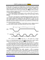
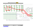
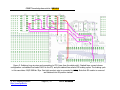
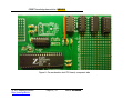
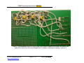
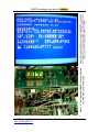
GR8BIT knowledge base article #KB0009
Oct 12, 2012
Severity: Information
Eugeny Brychkov (RU)
Accelerating your GR8BIT
Introduction
The dream of every computer geek is a technical and technological
excellence, more memory, larger hard disk, and higher speed. We have
committed on the GR8BIT specifications page that GR8BIT is expected to work at
4-20MHz, and here we will see if this promise is achieved, and if it is
achievable.
Warning!
Accelerated GR8BIT will not add value if you use machine for
gaming. All the MSX games will work fine at the standard 3.58MHz
clock speed. Even more, above specific clocking frequency level
accelerated GR8BIT is not guaranteed to work 100% properly in
terms of representation of the graphics.
Accelerated GR8BIT will add real value in terms of computing power.
There’s absolutely no goal to make GR8BIT a super-computer, and this
document rather describes technological experiment and endeavor to show the
flexibility of the MSX architecture and give another piece of important
experience.
Special thanks to Alwin Henseler (NL) for sharing his experience about his
Super-Turbo, for his advices on circuit design and for reviewing this KB article.
How it works, and how it stops working
If we are talking about the computer’s speed, we need to consider local and
global clocks using within it. Clock signal is fed to the CPU, to the GR8BUS and
all devices attached to it, to slowdown circuit and to the slot board (and thus
© 2012 Eugeny Brychkov
http://www.gr8bit.ru
Page 1 / 17
Status: Released
GR8BIT knowledge base article #KB0009
devices within slots 1 and 2). By default there’s one global clock signal, supplied
by the VDP to the GR8BUS and spread throughout the system (CPU board’s SJ1
and SJ7 are closed, and video board’s SJ1 is closed). It equals to 3.58MHz, and
strobes slowdown circuit in terms of wait state count, M1 wait state processing,
serves as reference frequency for PSG on the I/O board, SCC in the slot board or
converter board, and other devices.
If we change GR8BUS clocking speed, it will not affect PSG as I/O board is
designed to hold dedicated clock generation circuit, but other devices will be
affected.
CPU board is also designed to hold dedicated clock generation circuit, and it
can be used to supply global clock signal to the GR8BUS (if CPU board’s IC1 and
other related elements are installed, and video board’s SJ1 is open). You can
vary system speed by varying nominal of the XTAL1. But increasing speed will
decrease clock period relative to the specific chip specifications, and those chips
may not survive proper operation.
Let’s consider the most vital case, video display processor, which is required
for proper system operation and dialogue between you and your GR8BIT.
Figure 1. Example of the waveforms (scales are not kept)
VDP is driven by the IORQ signal (fig. 1). This signal has a length
(taccess_cycle), has active phase (tactive), and inactive phase (tinactive). Let’s simplify
situation and assume that two consecutive IORQ signals address VDP.
During the active phase, VDP samples data from the data bus or puts its
own data on the data bus. VDP works with specific speed and if tactive is less than
it can serve, VDP will not be able to sample correct data from the data bus (on
CPU write), as well as be too late to supply its data to the CPU (on CPU read). If
you’ll look into VDP datasheet, this minimal time equals to 186 nanoseconds and
typical value – 700ns (page 121).
Inactive phase timing is also vitally important – VDP is processing
information during this period of time. It may need to read data from the video
memory, or perform specific hardware-accelerated operation. Look into the same
data sheet, and you will see that minimal inactivity time varies between 2µs and
© 2012 Eugeny Brychkov
http://www.gr8bit.ru
Page 2 / 17
Status: Released
GR8BIT knowledge base article #KB0009
8µs (depends on the VDP command phase and operation requested). At CPU
clock speed of 3.58Mhz, 8µs equals to 28.5 T-cycles. To compare, one NOP
command takes 4 T-cycles, two EX (SP),HL command takes 38 cycles.
Therefore, increasing GR8BIT system clock frequency decreases length of
T-Cycle, and thus effective time dedicated for VDP data sampling and processing,
and at some critical value VDP stops working correctly. First it exhibits as small
artifacts on the screen, and as speed increases makes machine stop working
properly.
With GR8BIT you have flexibility to adjust length of the active phase of the
control signal using its slowdown circuit, but it has limitation of 15 additional wait
states, and does not allow lengthening time of signal inactivity.
Option #1: varying GR8BIT global speed with CPU board’s crystal
This option allows to slightly increase the processing speed of the machine.
No major hardware/design modifications are required. Here’re the steps to
achieve the results:
1. De-solder video board’s SMD jumper SJ1 to stop VDP supplying system
clock from its CPUCLK output. Note that VDPCLK will still be present on
the GR8BUS and can be used as a reference or source clock for your
devices;
2. Ensure SJ2 of the video board is soldered so that every VDP access would
activate slowdown circuit and you are able to tune number of VDP waitstates;
3. Ensure SJ1 and SJ7 are soldered on the CPU board, supplying clock signal
from XTAL1-based circuit to the GR8BUS as well as to the CPU;
4. Solder CPU board’s clock circuit components: socket for IC1, R1, C1 and
C2, and R2’
5. Solder 3.579545Mhz crystal as XTAL1 (supplied within GR8BOX);
6. Put IC1 in (supplied within your GR8BOX), install CPU board into GR8BIT,
and start it to ensure that it works.
The drawback of this implementation that global clock frequency changes,
leading to changed pitch of PSG and SCC music.
Your homework: try different crystals to see at which its nominal you notice
artifacts on the screen/GR8BIT does not start, varying number of wait-states
inserted using SW1 main board’s switch. Also ensure that this switch has position
#5 turned off (for modified slowdown circuit – turned on), and position #6
turned on (so that additional wait-states would apply also to PPI and RTC access
cycles).
© 2012 Eugeny Brychkov
http://www.gr8bit.ru
Page 3 / 17
Status: Released
GR8BIT knowledge base article #KB0009
Option #2: performing CPU suspend
This option has a right to exist, however after implementing it and testing
the system we decided to discard this option completely for the reason that it
was almost impossible to play games which heavily used VDP and PSG resources
due to game play snatching including video effects and music/audio effects.
The idea is that system clock stops for predefined period of clock cycles
when specific conditions are met – we used condition of IORQ (I/O port access)
deactivation to accommodate the lengthened inactivity period of time (activity
period of time is still variable using slowdown circuit of the main board).
If you are interested to know more about this option, or interested in
schematic, please let us know. It requires 3 additional chips to be installed onto
CPU board, and some other very minor modifications.
Option #3: separating CPU clock supply and system (GR8BUS)
clock, braking CPU clock to the nominal speed at
specific circumstances
This option is more complicated to implement, but allows to significantly
speed systems’ computing power without adverse effects exhibited by the option
#2. In our tests the maximal CPU clocking frequency we achieved with proper
system (and VDP in particular) is 12MHz. With crystal of 14.318MHz system did
not start at all in its maximal (in this design version) wait-state and brake
settings configuration. With 10MHz Z80 CPU provided within your GR8BIT you
can use 10MHz crystal, with 20MHz CPU we recommend to use 12MHz crystal.
After modification you will have GR8BIT storage subsystem and most
Konami games working (with proper sound). In gaming mode (with massive VDP
access) average speed of the CPU is braked to 3.58MHz, in computational mode
(when CPU does not perform port I/O access) CPU runs at full speed equal to the
value of the crystal of the CPU board.
We used simple condition to trigger CPU speed braking – activation of the
IORQ line. As soon as it activates, system starts getting clock signal from
another, “low speed” clock source, which ensures proper operation of the
external and internal devices like VDP (ports 98h-9bh), RTC (ports 0b4h-0b5h),
PPI (ports 0a8h-0abh), GR8BIT storage subsystem (ports 0a4h-0a5h) and many
others. As you will see from the explanation below, you have a freedom to
choose other (additional) signals to trigger braking, and have some options to
tune how braking system works and for which time CPU clock signal is braked.
Let’s look onto fig. 2. There’re six input signals for the braking circuit in this
implementation –
© 2012 Eugeny Brychkov
http://www.gr8bit.ru
Page 4 / 17
Status: Released
GR8BIT knowledge base article #KB0009
•
•
•
•
CLKHI, the high frequency clock signal, generated by the CPU board’s
crystal;
CLKLO, the standard VDP output frequency, for GR8BIT it is 3.58MHz;
IORQ as the trigger for braking. Note that you can combine different
triggering signals using simple logic (e.g. AND elements, if all signals are
active negative). The only requirement is that this composite triggering
input signal is active low;
Three (ACTx) as other optional triggering signals for braking (of your
choice);
and one output signal, CPUCLK, which clocks CPU (and some other circuits if you
choose so – read on).
Here’s a description of the functions of the logic elements on the schematic:
• IC5A: 4-input NAND logic gate, which outputs high level in case any of
input lines go low – e.g. IORQ on pin 1 goes active. You can connect 3
more low-active signals (e.g. slot select signals);
• IC5B: 4-input NAND logic gate, which suspends clocking impulses to the
counter IC4A;
• IC4A/IC4B: these are counters which count clock cycles supplied to
them, and present number of cycles counted on their outputs in binary
representation. These two 4-bit binary counter elements are daisy-chained
to form one 8-bit binary counter. This daisy-chained structure outputs a
positive-edge impulse BRAKE . Minimal number of cycles counted (if you
choose to connect pin 3 of IC5A to the pin 3 of IC4A, is 0 or 1/2 (depends
on the phase of its input clock at pin 1), maximal number of cycles
counted (if you choose to connect pin BRAKE to the pin 8 of IC4B) is 128
or 128.5 its input clock cycles at the pin 1 of IC4A. The selection of the
number of cycles which activates signal BRAKE can only be a power of 2
– 0 (20, pin 3), 2 (21, pin 4), 4 (22, pin 5), 8 (23, pin 6), 16 (24, pin 11), 32
(25, pin 10), 64 (26, pin 9) and 128 (27, pin 8). It does not look like a
great set of options, but it is enough to flat-tune to the acceptable level of
system reliability. You can add another counter in the same way as IC4,
and increase number of cycles counted above 7th power of 2. Moreover,
you have a flexibility to choose the IC4A clock source, which is used to
calculate number of cycles – either CLKHI, or CLKLO – and it is clear that
with CLKHI you can set number of cycles versus brake time more
precisely, however maximal absolute interval of time for IC4 to generate
strobe/triggering signal will decrease appropriately.
• IC3A/IC3B/IC6 is a reliable clock switching circuit, developed by the
Alwin Henseler (NL), and published and implemented in his Super-Turbo
device back in 1998.
© 2012 Eugeny Brychkov
http://www.gr8bit.ru
Page 5 / 17
Status: Released
GR8BIT knowledge base article #KB0009
Figure 2. Schematic of the braking circuit. Input signals are on the left (2+4), and output is on the right (1)
© 2012 Eugeny Brychkov
http://www.gr8bit.ru
Page 6 / 17
Status: Released
GR8BIT knowledge base article #KB0009
After the reset condition exact function of the IC5/IC4 depends on how IC4
initialized: if its output connected to BRAKE initialized in high level, IC5B’s
output is set to 1, counter does not receive clocking signal, and system starts at
CLKHI clock; if output connected to BRAKE is initialized in low level, system
starts at CLKLO clock, selected clock is passed through IC5B to the counter. As
soon as counter reaches the state when output connected to BRAKE becomes
high, BRAKE deactivates, clock stops being supplied to the counter, and system
runs at CLKHI speed. Thus system reaches stable state of running at CLKHI
speed within maximum 255 IC4A’s clock cycles (full loop of 256 states minus
one).
State changes as soon as IORQ (or any other triggering (ACTx) ) signal
goes low. It immediately clears the counter setting CRES signal high, also
resetting BRAKE signal low, thus system switches to CLKLO now on. This
“counter reset” state lasts until respective triggering signal is released (become
inactive), and CRES signal goes low. From this time counter starts to count (as
chosen clock signal is passed to the IC4A through IC5B).
If there’s another triggering signal activation occurs, counter IC4 got reset
again, and counting restarts.
If no following triggering signal occurs within the timeframe when IC4
counter reaches value defined by the connection of the BRAKE line, BRAKE
signal goes high, and clock switching circuit starts supplying CLKHI to the
CPUCLK line. At the same time IC5B’s input 9 becomes low, and disables further
counting (IC5B will always output high level to the IC4A clock input). Therefore,
when counter reaches predefined number of cycles, it is stopped and system
switches to high speed. This state is stable, and changes when any of triggering
signals activate next time.
Now let’s consider how clock switching circuit works. It has three inputs:
CLKLO, CLKHI, and BRAKE , and one output, CPUCLK, which is expected to be
equal to CLKHI if BRAKE is high level, and CLKLO if BRAKE is low level.
After the reset condition, BRAKE is high level for a long time (relative to
CLKHI and CLKLO), and whatever frequency is present on IC6’s pin 7 (STAGE) ,
IC3A is in high state, and IC3B is in high state too (look carefully – you will see
that IC3A and IC3B are “daisy-chained” – positive output of IC3A is serving as
data input to IC3B, and they both are clocked in by the same signal STAGE).
Therefore, IC6 inputs A and B are both in high level, selecting 1C3 input (CLKHI)
for STAGE output and 2C3 (also CLKHI) for CPUCLK output. This circuit is in
stable state.
As soon as BRAKE signal goes active (low), on the next positive edge of
CLKHI (which went through IC6’s input pin 1C3, out through 1Y output in to
STAGE signal), IC3A latches low level. IC3B remains in high level, and IC6’s “BA”
input pin combination becomes 01 (binary), selecting 1C1 for STAGE signal
© 2012 Eugeny Brychkov
http://www.gr8bit.ru
Page 7 / 17
Status: Released
GR8BIT knowledge base article #KB0009
(CLKLO), and 2C1 for CPUCLK. Please note that at the time, when STAGE goes
high and locks low level in IC3A, CPUCLK is equal to STAGE, and also in high
level. So when this transition of “BA” is performed, CPUCLK is sourced from input
2C1 which is in high level, and CPUCLK does not go low when CLKHI or CLKLO
go low.
At this time STAGE is equal to CLKLO, and on the next positive edge of this
signal, IC3A does not change state (it is already low as BRAKE is active), but
IC3B changes state to low, locking it from IC3A’s output. Now combination “BA”
of the IC6 source select inputs is equal to 00, and 1C0 is selected for STAGE
signal (no change), and 2C0 is selected for the CPUCLK signal (which becomes
equal to CLKLO – which just transitioned from low to high level, and is in high
level).
All further cycles, until BRAKE goes inactive, STAGE is equal to CLKLO,
and CPUCLK also equal to CLKLO, supplying low frequency to the CPU. As we see
transition was performed seamlessly, with probably small suspension when
CPUCLK is high during transition of low level from IC3A output to IC3B’s output.
When BRAKE goes inactive, on the next positive edge of STAGE (which
equals to CLKLO) IC3A locks high level, and “BA” of IC6 becomes 10, switching
STAGE to 1C2 (CLKHI) and CPUCLK to 2C2 (high level). The same hint works
here – CPUCLK just became high level before switching to 2C2 input, and remain
in high level while “BA” is equal to 10. On the next positive edge of STAGE
(=CLKHI), IC3B locks high level from output if IC3A, and “BA” becomes 11,
switching STAGE to 1C3 (no change, stays CLKHI), and CPUCLK to 2C3 (from
high level to CLKHI’s high level phase), and CLKHI continues to “clock out”
through the CPUCLK line to the CPU, making it run at the full speed. As you see,
again, transition between CLKLO and CLKHI was seamless, with probably small
suspension at high level.
Now, as you understand how the depicted circuit works, let’s see how it fits
into your GR8BIT.
• You will need four chips, one 74AC20, one 74AC74, one 74AC393 and one
74AC153 in DIP packages (not supplied within your GR8BOX), note that
they all should be CMOS family – either AC (fast) or HC (slower but
consumes less power) one 68 Ohm resistor (de-soldered from the R2
position), four IC sockets (three 14-pin and one 16-pin), four 0.1µF
decoupling capacitors and a hank of air-wire;
• Apply KB0001, replacing CPU board’s 22KOhm resistor packs with
10KOhm resistor packs. They will ensure the increased steepness of the
positive edge of the TTL-level address, data and control signals on the
increased system/CPU speeds;
• Ensure that video board’s SJ1 “CLKOUT” SMD jumper is soldered in,
supplying standard 3.58MHz frequency to the GR8BUS – it will be used by
the PSG, SCC and other devices on the bus;
© 2012 Eugeny Brychkov
http://www.gr8bit.ru
Page 8 / 17
Status: Released
GR8BIT knowledge base article #KB0009
•
•
•
•
•
•
Ensure that CPU board’s SJ1 “SYSCLK” SMD jumper is soldered in
(supplying GR8BUS clock to the CPU board), and SJ7 “CPUCLK” SMD
jumper is not soldered in (not supplying GR8BUS clock to the CPU chip);
Remove CPU board’s R2 resistor, and set it aside to solder as R8 later;
Ensure CPU board’s SMD jumper SJ4 “GTC” is not soldered (as gate C of
IC1 will be used in the braking circuit;
Solder CPU board’s clock generation circuit: socket for IC1, C1, C2, R1,
and XTAL1;
Solder sockets for IC3, IC4, IC5 and IC6, RN5 and R8, and connect them
as shown on fig. 3, fig. 4 and fig. 5. Please
pay attention to the dashed wires, which
show maximal (in terms of length of braking
period of time) configuration. You can choose
different settings according to the circuit
diagram on fig. 2;
Solder decoupling capacitors in point-to-point
manner (fig. 7). Ensure their pins do not
short-circuit and any pins/wires in the circuit.
Now your GR8BIT has two clock systems running simultaneously – CLKLO,
which is generated by the VDP, and has default frequency of 3.58MHz, and
CLKHI, which runs according to the crystal you installed as XTAL1 of the CPU
board. See fig. 6 and fig. 7 for the images of our test CPU board.
© 2012 Eugeny Brychkov
http://www.gr8bit.ru
Page 9 / 17
Status: Released
GR8BIT knowledge base article #KB0009
Figure 3. Soldering short air-wires (view from the solder side)
© 2012 Eugeny Brychkov
http://www.gr8bit.ru
Page 10 / 17
Status: Released
GR8BIT knowledge base article #KB0009
Figure 4. Soldering remaining short air-wires and connecting with IC1 (view from the solder side)
© 2012 Eugeny Brychkov
http://www.gr8bit.ru
Page 11 / 17
Status: Released
GR8BIT knowledge base article #KB0009
Figure 5. Soldering long air-wires and connecting to CPU (view from the solder side). Dashed lines connect chosen
configuration: red dashed line feeds CLKLO to the IC4, and pink dashed line selects 128 braking cycles. The braking cycle
in this case takes 128/3.58MHz=35µs. Red right-most air-wire is connected to IORQ . Note that R2 resistor is removed
and soldered into R8 position instead
© 2012 Eugeny Brychkov
http://www.gr8bit.ru
Page 12 / 17
Status: Released
GR8BIT knowledge base article #KB0009
Limitations: there’re several issues in this implementation which may, at
some circumstanced, show incompatibility with genuine MSX standard:
• If you recall slowdown circuit is supplied with the clocking signal from the
GR8BUS. While slowdown circuit built on IC45 will work properly, M1
wait-state circuit, built on IC16, will get problems. It is designed to be
supplied with CPU generated M1 signal and supplied to the CPU clock
signal – and it is vitally important because M1 signal phase and actions
happen within the specific state of CPU clock signal (there’s a positive
edge of the clock signal while M1 us active [low] and this low M1 gets
properly locked into the IC16A trigger). In our current dual-clock-supply
design, IC16A is supplied by the CLKLO, while CPU is supplied with CLKHI,
thus correct phase/edge of clock signal on the IC16A’s input 3 is not
guaranteed throughout the M1 activity time – and it leads to the loss of
the M1 CPU cycles wait-state required by the MSX standard. In most
circumstances when you have prolonged number of slowdown cycles (set
up by SW1 of the main board), this issue will not present problems, but
when timing becomes tight (mostly – for VDP) you may notice artifacts on
the screen. To fix this issue and make M1 wait-state circuit work properly,
you will supply CLKHI to the pins 3 and 11 of the IC16 to ensure that M1
and clock signal supplied coincide in expected way when M1 wait-state is
required. Your homework: identify which conductors you have to cut
(hint: only two), and air-wires between which points you have to put in
(hint: only two).
• Very similar to the issue described above – CPU cycles become “detached”
from their expected GR8BUS clock phases, and cartridges based on DRAM
memory will not work (they use clock signal to multiplex address into the
DRAM chips). The solution is to supply CPUCLK clock from the braking
circuit rather than from GR8BUS, and add triggering signal to braking
circuit which would activate it on respective slot access (do not forget
(ACTx) signals are active low).
© 2012 Eugeny Brychkov
http://www.gr8bit.ru
Page 13 / 17
Status: Released
GR8BIT knowledge base article #KB0009
Figure 6. Our acceleration test CPU board, component side
© 2012 Eugeny Brychkov
http://www.gr8bit.ru
Page 14 / 17
Status: Released
GR8BIT knowledge base article #KB0009
Figure 7. Our acceleration test CPU board, solder side (crystal is soldered from solder side because its
pads at the component side were damaged due to frequent soldering/de-soldering – see fig. 6)
© 2012 Eugeny Brychkov
http://www.gr8bit.ru
Page 15 / 17
Status: Released
Figure 9. The frequency GR8BIT is running during
the MSX-DOS command prompt
Figure 8. Running CHKSPD on the accelerated GR8BIT: as CHKSPD
is not designed for variable speed designs, it displays slightly wrong
results. Value of XTAL1 installed is 12MHz, not 13MHz.
GR8BIT knowledge base article #KB0009
© 2012 Eugeny Brychkov
http://www.gr8bit.ru
Page 16 / 17
Status: Released
GR8BIT knowledge base article #KB0009
Sources and information for further reading:
•
•
•
•
•
•
•
Henseler, A. (2012) MSX Super Turbo, available online at
http://bitcycle.org/retro/msx/super_turbo/ (accessed 12-Oct-2012)
Zilog Inc. (2004) Z80 Family: CPU User Manual, available online at
www.zilog.com/docs/z80/um0080.pdf (accessed on 12-Oct-2012)
ASCII Corporation, Nippon Gakki Co. (1985) V9938 MSX-Video
Technical data book: Part 2 “LSI data sheet”, available online at
http://www.msxarchive.nl/pub/msx/docs/datasheets/v9938.pdf
(accessed on 02-Oct-2012, hosted on MSX Assembly Page)
NXP Semiconductors (2012) 74HC74, 74HCT74 Dual D-type flip-flop
with set and reset positive edge-trigger Product data sheet, available
online
at
http://www.nxp.com/documents/data_sheet/74HC_HCT74.pdf
(accessed on 12-Oct-2012)
NXP Semiconductors (2005) 74HC393; 74HCT393 Dual 4-bit binary
ripple counter Product data sheet, available online at
http://www.nxp.com/documents/data_sheet/74HC_HCT393.pdf
(accessed on 12-Oct-2012)
Texas Instruments (2003) SN54HC153, SN74HC153: Dual 4-line to 1line data selectors/multiplexers, data sheet, available online at
http://www.ti.com/lit/ds/symlink/sn74hc153.pdf (accessed on 12Oct-2012)
Wikipedia (2012) Point-to-point construction, available online at
http://en.wikipedia.org/wiki/Point-to-point_construction (accessed on
12-Oct-2012)
End of KB0009 “Accelerating your GR8BIT”.
© 2012 Eugeny Brychkov
http://www.gr8bit.ru
Page 17 / 17
Status: Released


![ZXmore-V11-ConstructionKit [1144.78] KB](http://vs1.manualzilla.com/store/data/005859049_1-e30fafda14586d16f36a324828eeb8d9-150x150.png)