1
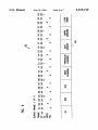
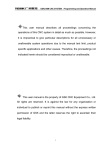
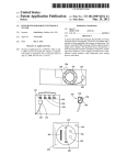
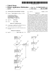
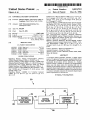
||||||m|||||mumlllllggmlggllitlglpn|||||||||||||||||||||||
United States Patent [191
[11] Patent Number:
Elpers et al.
[45]
Date of Patent:
5,519,719
May 21, 1996
[54] UNIVERSAL PATTERN GENERATOR
TE820A User’s Manual, Tekelec (1988), pp. 4.3-7, §4.3, pp.
4.5-1 through 4.5-2, §4.5, pp. 4.5-5, §4.5, pp. 4.6-1
[75] Inventors: Mark D. Elpers, Minneapolis; John C.
Lanphear, Eden Prairie, both of Minn.
through 4.6-2, §4.6, pp. 4.6-5 through 4.6-8, §4.6, pp.
4.7-3 through 4.7-6, §4.7.
' Operating Manual, 3776B PCM Terminal Test Set (Includ
[73] Assignee: ADC Telecommunications, Inc.,
Minneapolis, Minn.
[21] Appl. No.: 810,207
[22] Filed:
Dec. 19, 1991
[51]
[52]
Int. Cl.6 .................................................... .. G06F 11/00
US. Cl. ............................................ .. 371/27; 371/20.1
[58]
Field of Search .. ....................... .. 371/27, 22.1, 37.1,
371/39.1, 15.1, 21.3, 20.1, 20.5; 455/67.1,
67.4; 379/10; 375/10
[56]
4,810,958
Bell Communications Research, Technical Reference
TR-TSY-O00008, entitled “Digital Interface Between the
SLC 96 Digital Loop Carrier System and a Local Digital
Switch” (1987), pp. 3-1 through 3-14, §3.
Bellcore, Technical Reference TR-TSY-O0O499, entitled
References Cited
“Transport Systems Generic Requirements (TSGR) : Com
mon Requirements” (1988), pp. 9-1, §9.1.l.1, pp. 9-3
U.S. PATENT DOCUMENTS
through 9-6, §9.1.2, pp. 9-7, §9.2, pp. 10-1 through 10-14,
§10.2
3/1989 Mogi et al. ......................... .. 324/73 R
4,837,764
6/1989
4,964,124
10/1990
4,996,695
2/1991
Russello
.....
. . . . ..
Bunnett .... ..
371/20
371/15.1
Dack et al.
.... .. 375/10
5,072,178 12/1991 Matsumoto
324/158 R
5,265,089
ing Options 001, 002, and 004) Hewlett Packard (1984),
pp.4-4, §4-24, pp. 4-4, §4—25, pp. 4-4, §4-27, pp. 4-5,
§4-34, pp. 4-5, §4-35, pp. 4-5, §4-36, pp. 4-5, §4-37
pp.4-5, §4-38, pp. 4-5, §4-39, pp. 4-6, §4-40 pp. 4-6,
§4-41, pp. 4-6, §4-42, pp. 4-9, §4—56, pp. 4-30, §4-123,
pp. 4-30, §4-124, pp. 4-31, §4-129, pp. 4-31, §4-133, pp.
4-31, §4-134, pp. 4-31, §4-139, pp. 4-32, §4-144.
Primary Examiner—Robert W. Beausoliel, Jr.
Assistant Examiner—Phung My Chung
Attorney, Agent, or Firm—Merchant, Gould, Smith, Edell,
Welter & Schmidt
11/1993 Yonehara ................................ .. 370/15
[57]
OTHER PUBLICATIONS
Operating Manual, Pattern Generator/Error Detector,
3780A, Hewlett Packard (1983), p. 28, ‘H 7 and 8.
Operating Manual, 3781B Pattern Generator, 3782B Error
Detector, Hewlett Packard (1980), p. 3-3, ‘H 12 Through 15.
Programming Note, Quick Reference Guide for 3781B
Pattern Generator and 3782B Error Detector (1980), p. 3.
Phoenix, 5575A T1 Micro BERT Test Set, Operation -Sec
tion 3 (1989), pp.3-74 through 3-77, §3-6 and pp. 3-86
through 3-88, § 3-8.
Operating Manual, T-BERD 211 T-Carrier Analyzer
(1989), pp. 2-3, §2.3.1-1, pp. 2-3, §2.3.1-2, pp. 2-3,
ABSTRACT
A universal pattern generator generates a digital signal
pattern. The generator includes a user programmable device
for specifying a repeatable digital signal pattern. The pro
grammable device allows for the selection of a framing
structure having a number of channels. The programmable
device also has input means for inputting data into the
channels of the framing structure. A data set representing the
repeatable digital signal pattern is generated. The data set is
held in memory. A transmitter responsive to the data set held
in memory repeatably transmits the repeatable digital signal
pattern represented by said data set.
10 Claims, 7 Drawing Sheets
§2.3.1-13.
30
46
p
r32 42
PATTERN
(
T’
4s\
r34
‘ r36
GENERATOR
EDITING
T some
1'
28
44
38
state T
4o
US. Patent
OF
May 21, 1996
(D
N
Sheet 1 of 7
US. Patent
May 21,1996
Sheet 2 of 7
9.3
an
_/
£\:1~n\
.NKmo2hé5uz1o z6oc5ém2a8n wmuiétow
on
98
N.9. .
US. Patent
May 21, 1996
Sheet 3 0f 7
5,519,719
/52
FIG. :5
24
14
COUNTER
/54
RESET
/
58
_/
ADDRESS
<3
RAM
D 7
A
59
T 1
/
A o
\56
mc:—u-
/7o
AMV
/65
>
COUNTER
_/6"
RESET
65
../
ADDRESS
<3
D 7
A
T 1
RAM
A o
\62
68
/
ERROR/
SELECT
PAL
OUT
5,519,719
1
2
UNIVERSAL PATTERN GENERATOR
memory and a transmitter responsive to the data set repeat
edly transmits the repeatable digital signal pattern generat
ing the digital signal pattern.
TECHNICAL FIELD OF THE INVENTION
In one embodiment of the invention, the system allows for
the selection of errors to be generated in the data of channels.
The present invention relates generally to telecommuni
cation test systems. More particularly, the invention relates
Error data is generated corresponding to the errors selected
to pattern generators for use in telecommunication test
systems.
BACKGROUND OF THE INVENTION
10
To develop and test telecommunications equipment, a
and the data set generated has errors interjected therein as a
function of the error data.
According to another embodiment of the invention error
rates, bursts, or single errors are speci?ed for the framing,
logic, or line code of the repeatable digital signal pattern.
myriad of transmitting equipment products have been uti
Trigger circuitry interj ects the rate, burst or single errors into
lized to generate and apply to the telecommunications
the digital signal pattern.
equipment varying errored digital signal patterns. These
According to another embodiment of the invention, an
additional data set representing an additional repeatable
various equipment products, while functional, do not have
the ?exibility or control to adequately generate the errored
patterns necessary to thoroughly test the performance of
telecommunications equipment. For example, the HP 3781,
HP 3780, and HP 3782 pattern generators available from
Hewlett-Packard offer high bit rates, but only provide SF
superframing formats. Their error generation capabilities are
digital signal pattern is stored in the memory. The input of
the transmitter is switched between the data set for the
20
repeatable digital signal pattern and the additional data set.
The digital signal pattern represented by the data set and the
additional pattern represented by the additional data set are
alternately transmitted.
limited to producing a single error occurrence over which
According to yet another embodiment of the invention,
the user has no timing control, and only a limited selection
the input of the transmitter is switched between the data set
of error rates are possible. The Phoenix 5575A-Tl Micro
for the repeatable digital signal pattern and the additional
BERT available from Phoenix offers framed format genera 25
data set so that one iteration of either the digital signal
tion of various framing formats and line codes. Its error
pattern represented by the data set or the additional pattern
generation capabilities allow single error occurrence or error
represented by the additional data set is interjected into the
rate generation of line code and framing bits, however, it
transmittal of the other pattern.
does not control which bits are errored. The T—Bird 211
T-Carrier Analyzer, available from T-Bird, can generate any
number of consecutive frame bit errors, however, the gen
30
BRIEF DESCRIPTION OF THE DRAWINGS
eration of the errors is limited to the pressing of a switch
which generates the errored frame, limiting the switching
ability of generating a good frame and then an errored
framed when desired. The Tekelec TEB-ZOA-DSl Frame
FIG. 1 is a perspective view showing the universal pattern
generator of the present invention for use in testing tele~
35
Simulator and Analyzer, available from Tekelec, provides
various generating and erroring capabilities, but will not
provide ZBTSl line coding or the generation of Facility
communications equipment;
FIG. 2 is a block diagram of the software utilized with the
universal pattern generator of FIG. 1;
FIG. 3 is a block diagram of a RAM based transmitter of
Data Link messages and lacks the control necessary to
patterns. In addition, errors can only be inserted into uner
rored framed patterns, as opposed to inserting errors into an
the universal pattern generator of FIG. 1;
FIG. 4 is a block diagram of the AMI/ERROR/SELECT/
PAL of the transmitter of FIG. 3; and
already errored pattern.
The various pattern generator products utilize hardware
played during the use of the present invention.
quickly switch between errored and unerrored generated
customized or speci?c to the assembly of the user speci?ed
FIGS. 5-9 are softkey menus and screen displays dis—
45
channel content, framing, signal bits, etc. Therefore, when
changes are made in the speci?cations of the framing
patterns, data link formats, and the like, the products require
DETAILED DESCRIPTION OF THE
INVENTION
hardware modi?cations to meet the new requirements. Thus,
there is a need for a universal error pattern generator which
In the following detailed description of the invention,
provides ?exible and detailed pattern control to test the
performance of telecommunications equipment, and which
could replace the myriad of pattern generator products now
available.
55
SUMMARY OF THE INVENTION
The present invention is a system for generating digital
signal patterns. The system is prograrnmably controlled so
the user has ?exibility and detailed pattern control when
testing the performance of telecommunications equipment.
The system includes a user programmable device for speci~
references are made to the accompanying drawings which
form a part hereof, and which show by way of illustrations
speci?c embodiments in which the invention may be prac
ticed. It is to be understood that other embodiments may be
utilized and structural changes may be made without depart
ing from the scope of the present invention.
Referring to FIGS. 1-9, the preferred embodiment of the
Universal Pattern Generator of the present invention will be
described. FIG. 1 shows a perspective view of the Universal
Pattern Generator 10 coupled to test equipment units 16.
Generator 10 includes a user-programmable unit 12, includ
ing a computer or microprocessor and having a display 18,
fying a repeatable digital signal pattern. The programmable
softkeys 20 (and corresponding softkey display 90) and
device allows for selecting a framing structure having a
other input keys 22. The user programmable unit 12 allows
the user to specify a repeatable digital signal pattern and
plurality of channels, and includes an input for inputting data
into the channels. A data set representing the repeatable
digital signal pattern is generated. The data set is stored in
error the data in that pattern as will be described in detail
below.
5,519,719
4
3
SF, ESF, and SLC represent DSl rate superframing for
The user programmable unit 12 generates a data set
representing an errored or unerrored repeatable digital signal
mats. As is known in the art, the SF superframing format is
an assembly of 12 frames, each frame consisting of 24 8-bit
pattern and the data set is stored in memory of a RAM based
transmitter 14 via bus 24, a multi-bus in the preferred
embodiment. The transmitter 14 is responsive to the data set
samples of conversations, each 8-bit sample forms a separate
channel conversation. The frame also includes an extra bit
called the F-bit or the frame bit. Thus, each frame includes
stored in the memory and repeatedly transmits the repeatable
digital signal pattern represented by the data set by continu
193 bits per frame. In the SF superframing format, the F-bits
from the odd numbered frames, the “Ft bits” of FIG. 5, are
ously resetting a counter for addressing the memory of the
RAM based transmitter 14. Thus, the errored or unerrored
digital signal pattern is generated, transmitted, and applied
via line 26 to equipment units 16. The generator provides
set to the pattern 101010 to allow a receiving device to
10
frame. The F-bits from the even numbered frames, the “Fs
universal unerrored or errored T1 pattern generation and is
capable of adding new features and generating new patterns
therewith by creating new software, without redesigning the
hardware of the generator. It will be recognized by those
skilled in the art that T-1 refers to speci?c telecommunica
tions networks for transmitting data over speci?c framing
structures and timings and is well recognized by those
bits” of FIG. 5, are set to the pattern 001110 to allow a
15
carried on such networks is disclosed in Bellcore Technical
receiving device to identify which frame is the ?rst frame
and which is the last frame of a superframe.
FIG. 6 displays the structure of an ESF superframing
format screen. As is known in the art, the ESF superframing
format is an assembly of 24 frames. The F-bits from frames
4, 8, 12, 16, 20 and 24, the “Fe bits”, are set to the pattern
skilled in the art. A more detailed description of such
networks and the framing structure and timing of signals
maintain synchronization with the frames within the super
001011. These bits provide frame synchronization and
20
superframe synchronization. The F-bits from frames 2, 6,
10, 14, 18 and 22, the “CRC-6 bits”, are used as a check-sum
Reference TR-TSY-000499, “Transport Systems Generic
Requirements (TSGR): Common Requirements”, 1988.
of the previous superframe transmitted. The remaining
Software 30 associated with the user programmable unit
12 is shown in block diagram in FIG. 2. The software 30
includes pattern speci?cation software 32 for specifying a
error rate information.
F-bits, known as “FDL bits”, are generally used to relate
25
repeatable digital signal pattern in conjunction with the use
of editing software 34 in response to user input 28 and
generating a representative data set 42 of the repeatable
The last superframing format screen, FIG. 7, shows the
SLC, also referred to as SLC-96, superframing format. It is
an assembly of six SF superfrarnes. The F~bits from the odd
numbered frames, the “Ft bits” , are utilized in the same
manner as for the SF superframing format. The even num
speci?ed pattern. The representative repeatable data set 42 is
30
bered F~bits of frames 2—16 and 66—72, the “Fs bits”,
stored in computer RAM of user programmable unit 12.
function like the Fs bits of the SF superframing format. The
Editing software 34 allows the user through user input 46 to
remaining even Fs bits of frames 18—64 are FDL bits and
edit the structure of the representative data set 42. Software
provide a facility data link, generally used to transmit error
30 also includes mark errors software 35 for marking errors
in the representative data set 42 through user input and 35 rate information as in the ESF superframing format.
provides for generation of a marked error repeatable data set
In addition, as is known in the art, robbed-bit signalling
representative of the data set 42 and the user inputted
may be utilized in all three superframing formats to provide
marked errors applied to generator control software 86 in an
communication between the sources and sinks of the system.
additional array of data via line 37. An errored or unerrored
In the SF format, the 8th bit of every channel in the 6th and
repeatable pattern 40 is generated under control of generator
12th frames of every superframe are used as A and B
control software 36 when the repeatable data set 42 is
signalling bits. In the ESF format the 8th bit of each channel
directly applied thereto via line 38. The pattern 40 is a
in the 18th and 24th frames are used in addition to the 8th
marked errors pattern when the repeatable data set 42 and an
bits in the 6th and 12th frames to provide A, B, C, and D
additional array of data via line 37 is applied thereto.
signalling bits. The SLC format uses the 8th bit in the 6th
Further, under the control of generator control software 36,
additional errored patterns are generated via the unerrored,
45
errored, or marked error repeatable data set, as described
further below.
The softkeys 20 and corresponding softkey display 90,
other keys 22, and display 18, all of user programmable unit
12 form the user interface for generating the digital signal
and 12th frames like that of the SF format, only repeated six
times.
50
Each of these screens, FIGS. 5—7, when selected by the
user and under the control of speci?cation software 32,
displays the associated superframing structure. When there
is no user input, the X’s of the display screens 92 default to
l’s or FF, the hex code for all ones. When the SF, ESF, or
pattern 40. FIGS. 5-9 show various display screens 92 with
SLC softkey is selected, the associated softkey box is
softkey displays 90 for use in generating the digital patterns.
Softkey menu items shown by the softkey displays 90 in the
?gures shall be understood to represent also the correspond
highlighted to indicate that the user is in that particular
superframing structure menu. The other softkeys on the
main menu remain the same because they are not dependent
on whether the SF, ESF, or SLC key is selected.
User input 28 to specify an unerrored repeatable pattern is
inputted by the user via the screen and menu of softkeys of
55
ing software components carrying out the menu function.
The speci?cation, generation, and transmittal of an errored
or unerrored digital signal pattern will be described with
particular reference to these screens and softkey displays.
The pattern speci?cation software 32, FIG. 2, when
60
initiated displays a ?rst menu of softkey displays 90, FIG. 5.
Depending upon whether the SF, ESF, or SLC softkey is
FIG. 8 (under control of editing software 34) which appears
after the Edit Structure softkey of the screens, FIGS. 5—7, is
selected. The data, in hex code, for the channels, robbed-bit
signalling, number of super frames, FDL pattern length and
selected a different screen will be displayed therewith. If the
FDL content are inputted to specify an unerrored repeatable
SF softkey is selected then display screen 92 of FIG. 5 is
displayed. The screen 92 of FIG. 6 is displayed if the ESF
key is selected and the display screen 92 of FIG. 7 is
pattern by using either arrow key navigation around the
displayed if the SLC softkey is selected.
65
?eld, and then entering of data therein on the display, or
using certain alphanumeric keys of the user programmable
unit. Errors can also be speci?ed as described below.
5,519,719
5
6
The Next Channel softkey of the ?rst menu, FIGS. 5-7,
increments the channel displayed and displays the data
stored in the next channel. The Previous Channel softkey
decrements the channel displayed. The Mark Errors softkey
will be described below with regard to the mark errors
software 35. When the Load QRSS softkey is selected a
quasi-random pattern is created and loaded into the trans
mitter 14, as described further below, for transmission. The
errors software 35, FIG. 2. When an error is marked, the
actual data set of the repeatable signal pattern 42 does not
change but rather a bit is set in an additional data array so
that the marked data bit is inverted upon loading of trans
mitter 14 under control of generator control software 36. The
marked data bits are highlighted when the bits are displayed
on the main menu, FIG. 5, 6, or 7.
The following table shows representative bytes of an
unerrored generated repeatable pattern data set.
quasi-random pattern is generated according to the algo
rithm, xl5+ xl41+1=O.
TABLE 1
After or while the user is specifying the framing structure
and editing the screen ?elds, via the main menu, FIGS. 5—7,
l-Iex
speci?cation software 32, and, edit structure screen, FIG. 8,
fin'ther de?nition to the pattern to be generated can be
provided through the Edit Structure softkey of the main
Ordinary
unerrored “1"
01
0000 0001
+
l
Ordinary
02
0000 0010
—
l
00
0000 0000
NA
0
80
1000 0000
NA
0
polarity because
of line coding
Ordinary
20
correspond to that particular superframing format is dis
played. For example, the screen of FIG. 8 displays frame and
channel information of the ESF superframing format.
The edit structure screen, FIG. 8, allows the user to edit
Bit
negative
34. The edit structure screen 92 and softkeys 90 are the same
such parameters as the channel content, robbed-bit signal
Polarity
unerrored “1",
menu, SF, ESF, or SLC menus, FIGS. 5-7, and softkey menu
and screen of FIG. 8 under the control of editing software
whether you are in the SF, ESF, or SLC superframing format
mode, except that the frame and channel information which
Binary
unerrored “0”
“0" with repeat
bit set,
specifying end
of pattern
25
ling, the number of superframes in the pattern, the facility
When the user is satis?ed with the repeatable pattern he
has created and marked, a particular hardkey is selected to
data link (FDL), length and content, as well as the type and
initiate the appearance of the generator control menu asso
quantity of bi-polar violations (BPV’s), logic errors, and
framing errors. The user can specify, for example, robbed-bit
signalling by toggling the signalling function of screen 92,
30
allows the user to exercise control over the generator’s
pattern switching and error generation capability.
FIG. 3 shows the RAM based transmitter for generating
and transmitting the digital signal pattern. The RAM based
FIG. 8, from the “off” state to the “on” state, then navigating
through the ?eld to specify the content of the A, B, C or D
bits in each charmel by use of arrow key navigation or the
other keys to specify data where required.
ciated with the generator control software 36, shown by the
softkey display 90, FIG. 9. The generator control menu
selected. The AMI softkey toggles between each of these
selections and AMI line coding is the default setting if
transmitter 14 includes a side A 52 and a side B 60. Both
sides operate in the same manner. Side A includes RAM 56
connected to a counter 54, likewise Side B includes RAM 62
and counter 64. The data set 42 representing the repeatable
digital pattern is loaded into either side A or side B via the
bus 24. Power up initializes either counter 54 or 64 which
drives an address bus for addressing the data set. The
another is not selected. The Next Channel and Previous
Channel softkeys perform the same functions as before with
respect to the main menu, FIGS. 5-7. The Save File softkey
addressed data is applied to the input of the AMI/ERROR!
SELECT PAL 70. The PAL 70 will be described later with
regard to error generation. The seventh bit of the last word
The Boot Emulator softkey simply boots the emulator
35
which controls the generator in the product as now struc
tured. The AMI softkey allows the user to specify a line code
for the pattern. Either AMI, B8ZS, or ZBTSI may be
allows the user to save the ?le he just edited or initially 45 of data in the data set 42 representing the end of the
repeatable digital pattern as shown in Table l, resets the
speci?ed under a name of his own choosing in computer
counters 54 or 64 via lines 58 or 66 so that the data set is
memory and on disk or other storage media, and the Load
repeatedly transmitted.
By selecting the Load Generator softkey, FIG. 9, the data
set representative of the presently displayed pattern speci?ed
File softkey allows the user to call up previously saved ?les
in order to edit them.
Once the user has speci?ed the contents of the pattern by
using the screens associated with the edit structure menu,
by the user is loaded, under control of software 36, to
whichever side of the generator that is not currently being
selected for transmission. The line coding speci?ed in the
FIG. 8, under control of editing software 34, and the main
menu, Figs, 5, 6, or 7, under control of speci?cation software
32, the Edit Framing softkey of the edit structure menu is
selected. When selected, a digital data set 42 representative
55
of the repeatable digital signal pattern speci?ed is generated
and stored in computer RAM. Selecting the Edit Framing
softkey, displays on the screen, frame by frame, the actual
binary data set (display not illustrated).
After selecting the Edit Framing softkey, the softkey
Generator softkey remains highlighted until the loading is
60
display associated with the main menu once again is dis
played, including the Mark Errors softkey, FIGS. 5, 6, or 7.
As the binary data set is displayed frame by frame, the user
is allowed to mark F-bits for error generation by highlight
ing the bit using the arrow keys to navigate on the display
and selecting the Mark Errors softkey. The capability of
marking errors for generation is under the control of mark
Edit Structure screen and menu, FIG. 8, is performed at this
time. The data bits corresponding to the marked errors, if
any, are also inverted according to the additional data array
created under control of mark errors software 35. This Load
completed. Thus, if the RAM based transmitter is transmit
ting from side A 52, then it is possible to load into side B 60.
The Load Generator softkey toggles between A and B. The
Switch to A softkey, when selected, forces the generator to
transmit from side A. This softkey is highlighted when the
generator is transmitting therefrom.
65
The user interface allows the user to load a new pattern
into side B as indicated above, during the transmission from
side A and indicates this by labeling the softkey Load
5,519,719
7
8
Generator B. This would of course be true when side B is
based transmitter 14. The edit structure screen, FIG. 8, and
transmitting, whereby the softkey for loading is labeled
pattern speci?cation software 32, allows the user to specify
Load Generator A. Likewise, the Switch to B softkey forces
the generator to transmit from side B and this key is
a rate, burst, or single occurrence for a logic error. The edit
structure screen, FIG. 8, indicates that the Logic Errors are
in the off state, however, the state can be toggled to indicate
single, burst or rate errors. When an error rate is selected by
highlighted when the generator is transmitting therefrom.
As previously presented, a digital signal pattern 40 can be
the user as the single, burst or rate states are toggled, an
additional display, shown as XX, allows the user to enter a
desired rate. The same is applicable for the frame error
generated under control of software 36 once it is speci?ed
via pattern description software 32 utilizing editing software
34. This is shown in the software diagram of FIG. 2, wherein
loop 38 applies the repeatable digital pattern data set 42
generated by the pattern description software directly to the
generator control software 36. This pattern can be generated
as speci?ed without errors being introduced therein. The
unerrored digital pattern 40 per the user input 48 is generated
as speci?ed by the user. Of course, the speci?ed repeatable
digital pattern itself could be an errored pattern, thus the
10
capabilities. The selection of these types of logic errors or
frame errors cause errors to occur on the ?y. These types of
errors are post-line code generated and may disturb any line
coding already performed on the data set. When a single,
burst, or rate is specified, the user has no control over where
the
error will occur. When a single, burst, or rate is speci?ed
15
for logic or frame errors, a timer is con?gured (not shown)
RAM based transmitter would transmit an errored pattern
without ever generating an unerrored pattern.
The apparatus and software of the present invention
which applies, via lines 78 and 80 of in/out 65, signals
representative thereof to the binary invertor 86 of PAL 70.
The invertor 86 then inverts the digital pattern data set bits
applied via data input lines 74 and 76 from output lines 59
interject errors into the speci?ed repeatable digital pattern to
generate errored digital signal patterns in a number of ways.
or 68.
Line code errors or bi-polar violations (BPV’s) are also
created by the user with the edit structure screen and menu,
As was previously discussed, the Mark Errors softkey of the
main menu, FIGS. 5, 6 or 7, allows the user to access the
repeatable data set 42 and mark any given framing bit for
inversion upon loading and transmission. Marking the error
does not invert the actual data bit of the data set stored in
computer RAM, but rather a bit is set in an additional array
as previously described above and used to invert the bit prior
to line coding and when the repeatable data set is loaded in
transmitter 14. The data set 42 stored in computer RAM
FIG. 8, and PAL 70 of transmitter 14. A single, rate or burst
25
con?gured (not shown) which applies via line 82 and 84 of
in/out 65, signals representative thereof to the AMI encoder
30
pattern, accordingly. The user has no control over where in
In the present invention, software has not been written to
the pattern this BPV erroring will take place.
As may be appreciated, software could easily be written
allow all the bits, just the framing bits, of the speci?ed
repeatable digital pattern to be marked for error generation
per the Mark Errors softkey. It should be readily apparent to
to allow the user to specify which bits (framing, data,
signalling, etc. ) in the pattern are to be selected for logic or
BPV errors when utilizing the burst, or rate generating
capabilities. The hardware of the present invention would
support such software.
Although the present invention has been described above
in a preferred form, those skilled in the art will readily
appreciate that various modi?cations may be made to it
one skilled in the art that software to mark errors for any of
the speci?ed bits can easily be created. The marked error,
because the bit in the repeatable digital signal data set is
inverted when loaded, prior to transmission and is repeat
edly transmitted, occurs every time the speci?ed repeatable
pattern is repeatably transmitted.
A logic errored digital signal pattern can also be generated
45
fying a repeatable digital signal pattern via the main menu,
FIG. 5, 6 or 7, and the edit structure menu, FIG. 8, and then
pattern into side A 60 of RAM based transmitter 14, a
50
an additional logic error created with the Mark Error softkey
or Edit Structure software, can be loaded into side B of the
a repeatable digital signal test pattern, said user pro
grammable means including means for selecting a
iteration of the errored pattern in side B is transmitted with
55
error control without interrupting the pattern framing. With
the use of the Switch A-B-A softkey any of the bits of the
repeatable digital signal pattern can be errored, including the
data bits. This errored pattern is generated under generator
control software 36. No additional software is required to
T-1 timing, comprising:
user programmable means for allowing a user to specify
transmitter 14. By selecting the Switch A-B-A softkey, one
the digital signal pattern 40 represented by the data set
loaded into side A. This provides the capability of single
without departing from the spirit and scope of the invention,
as bounded by the claims of the application itself.
What is claimed is:
1. A system for generating a digital signal test pattern for
use in a T-1 data transmission system carrying primary
signals formatted in any one of a plurality of predetermined
T-1 framing structures and transmitted in a predetermined
loading the data set representative of that digital signal
duplicate of the digital signal pattern loaded into side A, with
88 of PAL 70. The AMI encoder 88 generates the BPV or
line code error in the logic errored or unerrored digital signal
remains unchanged.
utilizing the Switch A-B-A softkey, or the ALT A-B-A-B
softkey, FIG. 9, of the generator control menu. After speci
BPV occurrence is speci?ed in the same manner as speci?ed
for the logic and frame errors discussed above. When a
single, burst or rate is speci?ed for BPV errors, a timer is
60
selected framing structure for said repeatable digital
signal test pattern, said selected framing structure cor
responding to a selected one of said predetermined T-l
framing structures and having a plurality of channels,
and input means for inputting data into said channels of
said selected framing structure;
means for generating a data set representing said repeat
produce the single error capabilities. In addition, by select—
ing the Switch A-B-A-B softkey, the patterns loaded in side
able digital signal test pattern, said means for generat
A and side B are alternately transmitted.
Both logic errors and line code errors can be generated in 65
grammable means;
the digital signal pattern by means of the edit structure
screen and menu, FIG. 8, and the PAL 70, FIG. 4, of RAM
ing a data set operatively connected to said user pro
memory means for holding said data set;
transmitting means responsive to said data set held in said
memory means for repeatedly transmitting said repeat
5,519,719
10
9
able digital signal test pattern represented by said data
framing structures and having a plurality of channels,
and input means for inputting data into said channels of
said selected framing structure;
set to a receiving device for testing a performance of
said receiving device at a rate selected to correspond to
said predetermined T-l timing;
means for generating a data set representing said repeat
able digital signal test pattern, said means for generat
ing a data set operatively connected to said user pro
error means for selecting errors represented by a data
entry for said channels inconsistent with said T-l
grammable means;
framing structure; and
memory means for holding said data set; and
transmitting means responsive to said data set held in said
means for generating error data corresponding to errors
selected, said means for generating a data set interject
ing errors as a function of said error data.
1O
2. A system for generating a digital signal test pattern for
use in a T-1 data transmission system carrying primary
signals formatted in any one of a plurality of predetermined
T-1 framing structures and transmitted in a predetermined
T-1 timing, comprising:
able digital signal test pattern represented by said data
set to a receiving device for testing a performance of
said receiving device at a rate selected to correspond to
said predetermined T-1 timing; and
15
user programmable means for allowing a user to specify
said user programmable means including means for
selecting at least one of a line code, robbed bit signal
ling, and data link messages for said repeatable digital
a repeatable digital signal test pattern, said user pro
signal pattern.
grammable means including means for selecting a
7. A system for generating a digital signal test pattern for
use in a T-l data transmission system carrying primary
signals formatted in any one of a plurality of predetermined
T-1 framing structures and transmitted in a predetermined
selected framing structure for said repeatable digital
signal test pattern, said selected framing structure cor
responding to a selected one of said predetermined T-l
framing structures and having a plurality of channels,
T-l timing, comprising:
and input means for inputting data into said channels of
said selected framing structure;
means for generating a data set representing said repeat
memory means for repeatedly transmitting said repeat
user programmable means for allowing a user to specify
25
able digital signal test pattern, said means for generat
a repeatable digital signal test pattern, said user pro
grammable means including means for selecting a
ing a data set operatively connected to said user pro
selected framing structure for said repeatable digital
grammable means;
signal test pattern, said selected framing structure cor
responding to a selected one of said predetermined T-l
framing structures and having a plurality of channels,
and input means for inputting data into said channels of
memory means for holding said data set;
transmitting means responsive to said data set held in said
memory means for repeatedly transmitting said repeat
30
said selected framing structure;
able digital signal test pattern represented by said data
means for generating a data set representing said repeat
able digital signal test pattern, said means for generat
ing a data set operatively connected to said user pro
set to a receiving device for testing a performance of
said receiving device at a rate selected to correspond to
said predetermined T-l timing; and
grammable means;
error means for interjecting errors into said digital signal
memory means for holding said data set;
transmitting means responsive to said data set held in said
pattern.
3. A system according to claim 2, wherein said error
memory means for repeatedly transmitting said repeat
means includes means for specifying one of a logic error
rate, logic burst errors, and a single logic error for said
able digital signal test pattern represented by said data
repeatable digital signal pattern and trigger means for inter
set to a receiving device for testing a performance of
said receiving device at a rate selected to correspond to
jecting said one of logic error rate, logic burst errors, and
said predetermined T-1 timing; and
single logic error into said digital signal pattern.
framing burst errors, and a single framing error for said
said transmitting means further comprises an input con~
nected to said memory means for receiving said data
set, and wherein an additional data set representing an
repeatable digital signal pattern and trigger means for inter
additional repeatable digital signal pattern is stored in
4. A system according to claim 2 wherein said error means 45
includes means for specifying one of a framing error rate,
said memory means, and further comprising means for
jecting said one of framing error rate, framing burst errors,
and single framing error into said digital signal pattern.
50
5. A system according to claim 2 wherein said error means
includes means for specifying one of a line code error rate,
line code burst errors, and a single line code error for said
switching the input of said transmitting means between
the data set for the repeatable digital signal pattern and
the additional data set for the additional repeatable
digital signal pattern, so that one iteration of one of said
repeatable digital signal pattern and trigger means for inter
repeatable digital signal pattern and said additional
jecting said one of line code error rate, line code burst errors, 55
repeatable digital signal pattern represented by said
and single line code error into said digital signal pattern.
6. A system for generating a digital signal test pattern for
data set and said additional data set, respectively, is
interjected into the other one of said repeatable digital
use in a T-1 data transmission system carrying primary
signals formatted in any one of a plurality of predetermined
T-l framing structures and transmitted in a predetermined
signal pattern and said additional repeatable digital
signal pattern that is being repeatedly transmitted.
8. A method for generating an errored digital signal
T-l timing, comprising:
pattern for use in a T-1 data transmission system carrying
primary signals formatted in any one of a plurality of
predetermined T-l framing structures and transmitted in a
user programmable means for allowing a user to specify
a repeatable digital signal test pattern, said user pro
grammable means including means for selecting a
selected framing structure for said repeatable digital
signal test pattern, said selected framing structure cor
responding to a selected one of said predetermined T-l
65
predetermined T-1 timing, comprising the steps of:
specifying a repeatable digital signal pattern by:
a) selecting a framing structure for said repeatable
digital signal pattern and corresponding to a selected
5,519,719
12
11
said predetermined T-1 timing for testing a per
formance of said receiving device.
9. A method according to claim 8 wherein said specifying
one of said predetermined T-1 framing structures,
said framing structure having a plurality of channels;
and
b) inputting data into said channels of said framing
step further includes selecting at least one of a line code,
robbed bit signalling, and data link messages for said
structure;
selecting errors for said data in said channels by
repeatable digital signal pattern.
selecting a data entry for a channel which is incon
sistent with said T-l framing structure;
10. A method according to claim 8 wherein said step of
generating said errored digital signal pattern by:
i) loading a data set representative of said repeatable
digital signal pattern and said selected error data
into memory of a transmitter; and
ii) repeatably transmitting said repeatable digital
signal pattern represented by said data set to a
receiving device at a rate selected to correspond to
10
specifying a repeatable digital signal pattern includes the
step of specifying one of an error rate, burst errors, and a
single error for at least one of framing errors, logic errors
and line code errors of said repeatable digital signal pattern.